multiscale modeling of the indentation of nickel-aluminum
TRANSCRIPT

M ultiscale M odeling o f th e Indentation of N ickel-A lum inum N ano-layers
by
Ishraq Shabib
B.Sc. in Mechanical Engineering,
Bangladesh University of Engineering and Technology,
Dhaka, Bangladesh.
A thesis submitted to the
Faculty of Graduate Studies and Research
in partial fulfillment of the requirements for the Degree of
Master of Applied Science
Ottawa-Carleton Institute for Mechanical and Aerospace Engineering
Department of Mechanical and Aerospace Engineering
Faculty of Engineering
Carleton University
Ottawa, Canada
August 2005
© Ishraq Shabib, 2005
Reproduced with permission of the copyright owner. Further reproduction prohibited without permission.

1*1 Library and Archives Canada
Published Heritage Branch
395 Wellington Street Ottawa ON K1A 0N4 Canada
Bibliotheque et Archives Canada
Direction du Patrimoine de I'edition
395, rue Wellington Ottawa ON K1A 0N4 Canada
Your file Votre reference ISBN: 0-494-10092-3 Our file Notre reference ISBN: 0-494-10092-3
NOTICE:The author has granted a nonexclusive license allowing Library and Archives Canada to reproduce, publish, archive, preserve, conserve, communicate to the public by telecommunication or on the Internet, loan, distribute and sell theses worldwide, for commercial or noncommercial purposes, in microform, paper, electronic and/or any other formats.
AVIS:L'auteur a accorde une licence non exclusive permettant a la Bibliotheque et Archives Canada de reproduire, publier, archiver, sauvegarder, conserver, transmettre au public par telecommunication ou par I'lnternet, preter, distribuer et vendre des theses partout dans le monde, a des fins commerciales ou autres, sur support microforme, papier, electronique et/ou autres formats.
The author retains copyright ownership and moral rights in this thesis. Neither the thesis nor substantial extracts from it may be printed or otherwise reproduced without the author's permission.
L'auteur conserve la propriete du droit d'auteur et des droits moraux qui protege cette these.Ni la these ni des extraits substantiels de celle-ci ne doivent etre imprimes ou autrement reproduits sans son autorisation.
In compliance with the Canadian Privacy Act some supporting forms may have been removed from this thesis.
While these forms may be included in the document page count, their removal does not represent any loss of content from the thesis.
Conformement a la loi canadienne sur la protection de la vie privee, quelques formulaires secondaires ont ete enleves de cette these.
Bien que ces formulaires aient inclus dans la pagination, il n'y aura aucun contenu manquant.
i * i
CanadaReproduced with permission of the copyright owner. Further reproduction prohibited without permission.

The undersigned hereby recommend to
the Faculty of Graduate Studies and Research
acceptance of this thesis
“Multiscale Modeling of the Indentation of Nickel-Aluminum Nano-layers”
submitted by
Ishraq Shabib, B.Sc.
In partial fulfillment of the requirements for the degree of
Master of Applied Science
Thesis Co-supervisor,
Professor Ronald E. Miller
Thesis Co-supervisor,
Dr. Linruo Zhao
Chair, Department of Mechanical and Aerospace Engineering
Professor J.C. Beddoes
Carleton University
August, 2005
ii
Reproduced with permission of the copyright owner. Further reproduction prohibited without permission.

A b stra ct
The present research work presents the multiscale modeling of nano-indentation
into nickel-aluminum nano-layers using the coupled atomistics and discrete dislo
cation (CADD) model. In this work, the model has been extended to study the
layered structures to reveal how the microscopic mechanisms lead to the observed
indentation responses. Simulation results showed that the misfit dislocations at the
interface played an important role to initiate the plastic deformation in the lay
ered structures. The movements of misfit dislocations and their dissociation events
from the interface were found to be affected largely by the stress field induced by
the indenter. Load-displacement and hardness-displacement plots for different Ni-Al
models were evaluated and their responses were compared with the behaviors of the
pure metals. The hardness trends for all simulation models displayed their depen
dence upon simultaneous contributions from the indentation size effect (ISE) and
the hardening effect. It was also observed tha t the atomistic consideration near the
interface captured the dislocation/interface interactions more accurately compared
to the continuum model.
iii
Reproduced with permission of the copyright owner. Further reproduction prohibited without permission.

A cknow ledgem ents
First of all I want to express my sincere gratitude to the Almighty Allah to give me
the strength, knowledge and patience to complete this task, which I believe the most
significant accomplishment in my life. Since last two years I have been accompanied
and supported by many people and it is now a pleasant opportunity to express my
gratitude to all of them.
I am deeply indebted to my supervisor Professor Ronald E. Miller whose wisdom,
guidance, and encouragement helped me to successfully finish this research work.
He taught me sincerely every important aspect of materials science and also showed
me the way to do the computational works efficiently. He was always there to listen
my problems and give me the advice. I am very glad to work with him.
I would like to share this moment of happiness with my parents who rendered gar
gantuan love and encouragement from home during the tenure of my research. I am
obliged for the enormous sacrifice they have been made since my childhood. Espe
cially, I am gratified to my sister, ‘Lora’, for the support and encouragement she
provided both to me and to our parents during my stay in Canada. I would like to
give my special thanks to my wife ‘Lagna’ for the inspiration, love and moral support
she provided throughout my research work. Her patience was tested to the utmost
by a long period of separation. W ithout their loving support and understanding I
would never have completed my work.
I wish I would never forget the company I had with my co-worker ‘Gladys’. I greatly
appreciate her thoughts, ideas and valuable hints in solving numerous problems. I
am thankful to the fellow research scholars from my Department, ‘Behrouz Shiari’
and ‘Denis Saraev’, for their valuable suggestions and guidance to carry out this
research. I also gratefully acknowledge the cooperation tha t I received from other
faculty members and administrative staffs of my department. I want to give my spe-
iv
Reproduced with permission of the copyright owner. Further reproduction prohibited without permission.

cial thanks to Dr. Linruo Zhao and Dr. Kuiying Chen from Institute of Aerospace
Research (IAR) of NRC, for their cooperation and valuable comments regarding my
thesis.
I would also like to express my gratitude to the Department of Mechanical and
Aerospace Engineering and the Faculty of Graduate Studies and Research of Car-
leton University and National Research Council (NRC) of Canada for giving me the
financial support throughout my masters program.
v
Reproduced with permission of the copyright owner. Further reproduction prohibited without permission.

To m y parents
vi
Reproduced with permission of the copyright owner. Further reproduction prohibited without permission.

C ontents
A b s t r a c t .................................................................................................................... iii
A ck now ledgem en ts ................................................................................................ iv
Table o f C o n t e n t s ................................................................................................ vii
List o f Figures ....................................................................................................... x
List o f T a b le s ............................................................................................................. xiii
N o m en c la tu re .............................................................................................................xiv
1 Introduction 1
1.1 Multilayer structures and their p roperties .................................................... 1
1.2 N ano-inden tation .............................................................................................. 3
1.3 Atomistic and multiscale modeling .............................................................. 3
1.4 Motivation of this re sea rch ............................................................................. 4
1.5 Thesis o u t l in e .................................................................................................... 5
2 Background M aterial and Literature R eview 7
2.1 Preparation of thin f i lm s ................................................................................ 8
2.1.1 Physical Vapor D ep o sitio n ................................................................ 8
2.1.2 Chemical Vapor Deposition ............................................................. 10
2.2 Film g ro w th ........................................................................................................ 11
2.3 Applications of thin film s................................................................................ 11
2.3.1 Electrical and Magnetic ................................................................... 11
2.3.2 Metallurgical and protective c o a t in g s ............................................ 12
vii
Reproduced with permission of the copyright owner. Further reproduction prohibited without permission.

2.3.3 O p tical.................................................................................................... 12
2.4 N ano-inden tation ............................................................................................ 12
2.4.1 Interpretation of load-displacement c u rv e ..................................... 13
2.4.2 Stiffness, Contact area, Modulus and Hardness measurement . 14
2.4.3 Factors affecting nano-indentation test d a t a ............................... 18
2.5 Hardening theories at the nanometer s c a l e .............................................. 22
2.5.1 Orowan M o d e l: ................................................................................... 22
2.5.2 Hall-Petch M odel:................................................................................ 23
2.5.3 Dislocation-Interface In te rac tio n ...................................................... 26
2.6 Computational a p p ro a c h ............................................................................... 31
2.6.1 Atomistic modeling scheme ............................................................ 32
2.6.2 Multiscale modeling s c h e m e ............................................................ 35
3 Coupled A tom istic and D iscrete D islocation (C A D D ) M ethod 42
3.1 Continuum Solution Procedure .................................................................. 44
3.2 Atomistic Solution P r o c e d u re ..................................................................... 47
3.3 Equilibrium configuration ........................................................................... 48
3.4 Dislocation Detection and P assin g .............................................................. 49
3.4.1 Dislocation D etec tion .......................................................................... 49
3.4.2 Dislocation P a ss in g ............................................................................. 50
3.5 Modification of the CADD m o d e l .............................................................. 51
3.5.1 Selection of the p o te n tia l................................................................... 53
3.5.2 Lattice constant calculation for A1 and Ni .................................. 55
3.5.3 Elastic modulus C a lc u la tio n ............................................................ 57
3.5.4 Model description for bilayer simulation ..................................... 59
3.5.5 Model description for multilayer sim ulation .................................. 63
viii
Reproduced with permission of the copyright owner. Further reproduction prohibited without permission.

4 R esults and analysis 68
4.1 Bilayer simulation re su lts ................................................................................ 68
4.1.1 Aluminum film on top of nickel su b s tra te ...................................... 69
4.1.2 Nickel film on top of aluminum s u b s tra te ...................................... 73
4.1.3 Load-Displacement curves for Al-Ni bilayer s y s te m s .................. 76
4.1.4 Hardness measurement for bilayer s y s te m s .................................. 78
4.1.5 Atomic level stress ca lcu la tio n ......................................................... 82
4.2 Multilayer simulation r e s u lts .......................................................................... 87
4.2.1 Ni-Al-Ni sy s tem .................................................................................... 88
4.2.2 Ni-Al-Ni system (without an atomistic region at the second
interface) ............................................................................................. 88
4.2.3 Load-Displacement curves for Ni-Al multilayer systems . . . . 91
4.2.4 Hardness measurement for multilayer s y s te m s ............................ 93
5 C onclusions and Future R ecom m endations 96
5.1 Summary of co n c lu s io n s ................................................................................ 96
5.2 Recommendations for future w o rk ................................................................ 99
ix
Reproduced with permission of the copyright owner. Further reproduction prohibited without permission.

List of Figures
1.1 Multilayer coating structure on Ti-6A1-4V substrate................................. 5
2.1 Load vs. Displacement cu rv e .......................................................................... 14
2.2 A cross section through an indentation showing various quantities
used in the an a ly sis ......................................................................................... 17
2.3 Schematic of the initial penetration depth on load vs. displacement
d a t a .................................................................................................................... 19
2.4 Geometrically necessary dislocations created by a rigid conical indenter 21
2.5 Effect of sinking-in and pile-up on the actual contact a re a ..................... 22
2.6 Single-dislocation based Orowan m o d e l ...................................................... 23
2.7 Pile-up of dislocations against a grain boundary under an applied
shear s t r e s s ....................................................................................................... 24
2.8 Hall-Petch plot for several Cu-based m u ltilay e rs ...................................... 26
2.9 Experimental observations and model predictions for tensile yield
stress vs. superlattice period for Cu/N i superlattices ........................... 29
2.10 Experimental observations and model predictions for hardness vs. su
perlattice period for TiN/NbN s u p e r la t t ic e s ........................................... 30
2.11 Schematic illustration of the solution procedure of the discrete dislo
cation m e th o d .................................................................................................... 37
2.12 The atomistic/continuum region for the QC m e th o d ............................... 38
2.13 The atomistic/continuum region for the FEAt method ........................ 40
2.14 The atomistic/continuum region for the CLS m e th o d ........................... 41
x
Reproduced with permission of the copyright owner. Further reproduction prohibited without permission.

3.1 Schematic illustration of the solution procedure for the CADD method 45
3.2 Position of the detection band to detect dislocations .......................... 50
3.3 Dislocation detection and passing across the atomistic/continuum in
terface in the CADD method ..................................................................... 51
3.4 CADD flow c h a r t ............................................................................................ 52
3.5 The functions comprising the Ni, A1 and NiaAl p o te n tia ls ................... 54
3.6 Bravais lattice vectors of Aluminum and Nickel .................................... 58
3.7 Bilayer simulation m o d e l............................................................................... 61
3.8 Atomistic region and the position of the layer interface between Ni
and A 1 ................................................................................................................ 62
3.9 Positions of the real atoms, interface atoms, pad atoms and the con
tinuum nodes in bilayer simulation m ode l.................................................. 63
3.10 Actual position of the interface in the continuum reg io n ...................... 64
3.11 Multilayer simulation m o d e l ........................................................................ 65
3.12 Positions of real atoms, interface atoms, pad atoms and continuum
nodes around the second atomistic reg io n .................................................. 66
3.13 Position of the detection band inside the second atomistic region . . . 67
4.1 Positions of the misfit dislocations along the interface of the Al/Ni
m o d e l ................................................................................................................. 70
4.2 Movements of the misfits and their dissociation from the interface . . 71
4.3 Dissociation of the misfit dislocations at different locations in the layer
in te rfa c e .............................................................................................................. 72
4.4 Dissociation of dislocation inside the l a y e r ............................................. 72
4.5 Accumulation of the dislocations in the aluminum la y e r ...................... 73
4.6 Position of the misfits along Ni/Al interface .......................................... 74
4.7 Movement and dissociation of the misfit dislocations at the Ni/Al
in te r fa c e .............................................................................................................. 75
xi
Reproduced with permission of the copyright owner. Further reproduction prohibited without permission.

4.8 Passing of dislocation across the Ni/Al in te rfa c e .................................... 76
4.9 Load-Displacement curves for different Al-Ni bilaver system ............. 77
4.10 Hardness variation with depth of penetration for different bilayer models 79
4.11 Hardness trends after first dislocation nucleation for different bilayer
m o d e ls ................................................................................................................ 81
4.12 Residual stress distribution along the Ni/Al in te r f a c e .......................... 83
4.13 The effect of indenter on the atoms in the atomistic region at different
indentation d e p th ............................................................................................. 84
4.14 Shear stress variation of the atoms located at the in te r f a c e ................. 85
4.15 Shear stress variation of the atoms located at 10.0/1 above and below
the interface ................................................................................................... 86
4.16 Deformation configuration of Ni-Al-Ni m o d e l........................................... 89
4.17 Deformation configuration of Ni-Al-Ni (without 2nd atomistic region)
m o d e l ................................................................................................................. 90
4.18 Load-Displacement curves for different Al-Ni multilayer system . . . . 92
4.19 Hardness variation with depth of penetration for different multilayer
m o d e ls ................................................................................................................. 94
4.20 Hardness trends after first dislocation nucleation for different multi
layer m o d e ls ....................................................................................................... 95
xii
Reproduced with permission of the copyright owner. Further reproduction prohibited without permission.

List o f Tables
3.1 Experimental and calculated properties of aluminum ........................... 55
3.2 Experimental and calculated properties of n ic k e l..................................... 55
3.3 Calculated in-plane elastic constants for alum inum .................................. 59
3.4 Calculated in-plane elastic constants for n ic k e l......................................... 59
4.1 Summary of the results obtained from all bilayer models ..................... 82
4.2 Summary of the results obtained from all multilayer models .............. 94
xiii
Reproduced with permission of the copyright owner. Further reproduction prohibited without permission.

N om enclature
CADD Coupled atomistic and discrete dislocation method
QC Quasicontinuum method
CLS Concurrent length scale method
FEAt Finite element and atomistic method
EAM Embedded atom method
ISE Indentation size effect
Al/Ni model Aluminum film on top of a nickel substrate
Ni/Al model Nickel film on top of an aluminum substrate
Al-Ni-Al model Aluminum and nickel film on top of an aluminum substrate
Ni-Al-Ni model Nickel and aluminum film on top of a nickel substrate
X W idth of the model (A)
Y Thickness of the model (A)
P Indenter load (el//A )
§ Displacement of the indenter (A)
A Area of contact (A2)
H Hardness (el//A 3)
$ Pair potential
F Embedding energy
p Electron density
rcut Cutoff radius
xiv
Reproduced with permission of the copyright owner. Further reproduction prohibited without permission.

rij Interatomic distance between atoms
R Relative radius of curvature
E* Reduced Modulus
E Young’s Modulus
v Poisson’s ratio
G Shear Modulus
A. /i Voigt-average elastic constants
b Burger’s vector
A Bilayer period
m Slip plane normal
Ac Coherency wavelength limit
Oij Atomic level stress tensor
e Strain
u Displacement
ao Lattice constant
C n, C 1 2 , Cqq Elastic constants
fIt Atomic volume at site i
xv
Reproduced with permission of the copyright owner. Further reproduction prohibited without permission.

Chapter 1
Introduction
1.1 M ultilayer structures and their properties
Measuring and understanding the mechanical properties of thin film structures, con
sisting of alternating nano-scale multilayers, have been a recent area of active in
vestigation due to their enhanced hardness, tensile strength, corrosion resistance
and wear resistance properties compared to monolithic coatings of the constituent
materials [1], [2]. Some of the nanolayered metals, ceramics and alloys even exhibit
super-elasticity tha t ensures large elongation of solids without failure at relatively
low temperature and high strain rates [3]. Early multilayer coatings consisted of a
layer of nitride or carbide and an oxide, such as TiN or TiC and A120 3, and were
used to improve the life of cutting tools. The nitride/carbide layer ensures strength
and the oxide layer provides corrosion resistance to make the structure very use
ful in cutting applications. Though the thickness of the individual layers of early
multilayer coating was of several microns thick, a new class of multilayer structure
has emerged that consists of very thin (2-10 nm) layers and exhibits extremely high
hardness [4]. Experimental results also showed tha t metallic multilayered structures
made of two kinds of metals, even those made from soft metals, exhibit significant
increase in yield and fracture strengths with decreasing bilayer thickness [1], [5]. This
enhancement is not easily attainable by traditional microstructures. However, below
a critical bilayer period, the hardness values may remain constant or even decrease
1
Reproduced with permission of the copyright owner. Further reproduction prohibited without permission.

with bilayer thickness [1]. The secret of such behavior actually lies in the plastic
deformation of these materials. Over the years, understanding of plastic deforma
tion of materials at nanometer length scale is a challenge in materials science. The
plastic behavior of materials at such a small length scale is mainly controlled by the
nucleation and motion of lattice dislocations [6]. Although, dislocations are sim
ple line defects of the materials, the ways those defects nucleate and interact with
each other and with grain boundaries, are very complex in nature [7]. In coarse
grained materials the motion of dislocations within individual grains is hindered by
the grain boundaries, which results in dislocation pile-ups against them. Further
reduction in grain size introduces more obstacles to the dislocation motion, thereby
making metal harder to deform. This strengthening mechanism is expressed by the
Hall-Petch relation. However, at very small grain sizes the Hall-Petch relation breaks
down and even becomes a reverse one [8]. Moreover, there are some other factors, i.e.
modulus mismatches, lattice parameter mismatches, gamma surface mismatches and
slip-plane mismatches between adjacent layers, that have also been attributed for
this enhancement [9]. A detail discussion about hardness enhancement at nanometer
length scale will be presented in Chapter 2. Though very high hardness or strength
has already been observed in many nanomaterials, in most of the cases they have
low ductility due to the physical nature of plastic deformation. But several investi
gations have also been carried out for materials having both of these two opposing
characteristics. Wang et al. [10] created a “bimodal” structure of micrometer-sized
grains embedded in a matrix of nanocrystalline grains that showed extraordinarily
high ductility, but also retained its high strength. In such structures, nanocrys
talline grains provide strength and the embedded larger grains stabilize the tensile
deformation of the material [10]. A few authors have proposed a so-called rotational
plasticity [11] that also led to high strength and ductility in nanostructured m ate
rials. Such occurrence became possible through the formation of a nanometer sized
2
Reproduced with permission of the copyright owner. Further reproduction prohibited without permission.

grain structure in which sliding can occur at grain boundaries. It is thus necessary to
explore all these underlying mechanisms that contribute to the enhanced mechanical
properties of materials that are highly desirable for engineering applications and can
be exploited to make “next-generation” materials .
1.2 N ano-indentation
During the last several years, nano-indentation testing has become an integral part
of modern materials science to characterize the mechanical behavior of materials
of very small volume. Although the test involves simply penetrating a specimen
of interest with an indenter, the information tha t can be achieved from this test
has much importance. In practice, the goal of such testing is to measure different
mechanical properties, i.e. elastic modulus, hardness and contact stiffness, of the
specimen under consideration from indenter load and penetration depth. Several
researchers proposed several ways to interpret the load-displacement curves and to
extract data from it for different materials, and the results showed good estimation
of such materials’ properties. Present research work is thus focused on simulat
ing such nano-indentation testing into layered materials to elucidate the underlying
mechanisms tha t contribute to the overall response of the system.
1.3 A tom istic and m ultiscale m odeling
As we have discussed in our previous sections there are im portant phenomena oc
curring at many different length scales that contribute to mechanical properties.
These length scales range from angstrom to micrometer. Since experimental mea
surements and conventional theoretical modeling based on a continuum approach
cannot offer a microscopic view of the physics at such small length scales, atomistic
simulations are becoming increasingly prominent in materials science to elucidate
the effects of defects, surfaces and other microstructural features. Predictions re-
3
Reproduced with permission of the copyright owner. Further reproduction prohibited without permission.

suiting from this atomic-level understanding are a vital source of information for
directing experimental research. Fully atomistic simulations are essential to analyze
atomic scale phenomena, but may involve millions of atoms to simulate the whole
structure. This may reduce the performance of computers for their limitations in
memory requirements and simulation time. To overcome this problem a multi-scale
material modeling approach has emerged, whereby atomistic modeling is used in
conjunction with a continuum approach to link both time and length scales. In the
multi-scale modeling approach, atomistic calculation is used in regions where atomic
scale defect nucleation and interaction effects are important, whereas a continuum
scheme is applied to the rest of the system by dividing it into linear elastic finite
elements to reduce overall computation time [12],[13],[14],
1.4 M otivation o f th is research
Nanolayer coatings find their applications in gas turbine engines in the aerospace
industry and also in the high-speed machining tools to protect erosion and wear.
Figure 1.1 shows a multilayer coating on Ti substrate, which consists of Ti, Cr and
TiN/CrN superlattice. Multilayer coating makes the structure hard, tough and envi
ronmental resistant. Hardness of such structure can be as high as 20-40 GPa. TiN is
hard compared to CrN, but the TiN/CrN superlattice coating exhibits much higher
hardness in comparison with monolayered TiN and CrN coating. In our present re
search work two different types of materials, Ni and Al, have been selected to create
different film-substrate systems to simulate this physical phenomenon. One of our
main objectives was to understand the different atomic scale phenomena, i.e. dislo
cation nucleation and dislocation-grain boundary interactions tha t contribute to the
macroscopic mechanical behavior of these film-substrate systems. A new multiscale
modeling approach, Coupled Atomistic Discrete Dislocation (CADD) method, has
been adopted to simulate the behavior of these systems during nano-indentation.
4
Reproduced with permission of the copyright owner. Further reproduction prohibited without permission.

Figure 1.1: Multilayer coating on Ti-6A1-4V substrate. The multilayer coating consists o f Ti, Cr and T iN /C rN superlattice (Picture obtained from NRC, ACE2003- AM TC, Sept 11, 2003).
1.5 T hesis outline
This thesis is divided into five chapters. This chapter provides a brief introduction
about multilayered structures at the nanometer length scale, their properties and
applications, different modeling schemes and motivation of this work. Chapter 2
is the literature review part of this thesis. It is mainly divided into two parts: a
brief discussion about different physical problems and the methods of study of those
physical problems. In the first part we will be discussing about thin films, their char
acteristics, preparation and applications. Moreover, nano-indentation in thin metal
films and strengthening theories at the nanometer length scale will also be discussed
in this part. In the second part, a brief review of atomistic modeling and different
multiscale modeling schemes will be presented. Results from atomistic simulation of
nano-indentation on bilayered and multilayered thin films will be discussed and some
results from experimental work on metal thin films will also be presented. Chapter
3 will mainly be focused on the coupled atomistic and discrete dislocation (CADD)
method. This is a multiscale modeling scheme tha t has been used to simulate the
problems in this thesis. The theory and solution procedure of the CADD method
5
Reproduced with permission of the copyright owner. Further reproduction prohibited without permission.

has already been published in [15],[16]. A brief review of the theory and solution
procedure will be discussed first and then the details of our modifications to the
existing CADD code will be presented. Simulations were performed on different
bilayered and multilayered film-substrate systems. Nano-indentation simulation re
sults and analysis of those results will be presented in Chapter 4. Chapter 5 presents
concluding remarks based on the results obtained from the present work and also
gives recommendations for future work.
6
Reproduced with permission of the copyright owner. Further reproduction prohibited without permission.

Chapter 2
Background M aterial and Literature R eview
Understanding of the fundamental nature of materials has dramatically increased
throughout much of the twentieth century tha t led to the development of materials
science and engineering. During this period a wide variety of metallic, polymeric,
nuclear, ceramic and electronic materials have emerged, and a number of reliable
methods to process these materials in bulk and thin-film forms have been developed.
Thin film processing is one of the oldest arts and one of the newest sciences tha t have
been subjected to countless investigations since the first films were fabricated more
than one hundred years ago. They were first employed as coatings of precious metals
and later found wide applications for corrosion protection. But in recent years thin
films play a crucial role in the high tech industries. Major exploitation of thin films
has been in microelectronics, whereas there are numerous and growing applications
in communications, optical, electronics, magnetic and tribological fields [17]. Thin
film structures in form of nano-scale multilayers exhibit high temperature stability,
enhanced hardness, yield strength, corrosion and chemical resistance properties that
make them very useful as a coating of the cutting tools, turbine and compressor
blades to improve their life [4],[2],[18],[8],[19],[5],[20]. The term “thin film” refers
to a very thin layer of gaseous, liquid or solid material, the thickness of which is
usually regarded as being between 2-10000 A. Because of extreme thinness, thin
7
Reproduced with permission of the copyright owner. Further reproduction prohibited without permission.

films have very little strength and cannot be made self-supporting. Thus, they
must be fabricated by deposition on to a suitable substrate. The main role of the
substrate is to provide mechanical support of the thin film [21]. The primary interest
in thin films is due to two effects. Firstly, a material in thin-film form sometimes
has im portant properties that differ from those of the material in bulk. As the
film becomes thinner the surface-to-volume ratios becomes larger and consequently
the surface usually influences the film’s properties greatly. The other cause is the
possibility of the miniaturization of electronic equipments, where thin films find one
of their most useful applications [22], [21].
2.1 Preparation o f th in films
There are number of methods available to fabricate thin films. The method to be
used will depend on the material to be deposited and the substrate itself. Among
numerous techniques, physical vapor deposition (PVD) and chemical vapor depo
sition (CVD) are probably the most widely used techniques for the preparation of
thin films [23]. In this section a brief review of these methods will be presented.
2.1 .1 P h y sica l V apor D e p o s it io n
Physical vapor deposition (PVD), the term tha t includes both evaporation and sput
tering [17].
Evaporation
This technique is by far the most used for the deposition of thin films. It is very
simple in essence. A vacuum or reduced pressure environment is created within
a chamber by a vacuum pump. The exact pressure used will depend upon the
particular type of film being produced. W ithin the chamber the material of which
the thin film is to be made, and the substrate on which the film is to be deposited
are placed. The thin film material acts as a source of vapor. The vapor source
8
Reproduced with permission of the copyright owner. Further reproduction prohibited without permission.

is usually placed in either a tungsten basket or an alundum crucible. Tungsten
wires, refractory metal sheets, electron beams can act as a source of heat. Thin
film material is heated until the metal vapor is evolved. Due to low pressure within
the chamber the molecules radiate out from the source and deposit on the substrate
[22], The evaporation rate, film uniformity and film purity depend upon the atomic
weight and the vapor pressure of the element, temperature and evaporation co
efficient, vacuum pressure in the system and the design of the source. These factors
not only affect the vaporization rate but also through chemical reactions during
evaporation and condensation can profoundly modify the structural, electrical and
optical properties of the film [23]. Moreover, the impurities that are initially present
in the source and the heater and those originate from the residual gases present in
the vacuum system have a profound effect in degrading many of the properties of
evaporated films [17].
Sputtering
When atoms having high energies strike a surface, it forces the material from the
surface to be ejected. This process is termed as “sputtering” . The material to be
deposited on the substrate in the form of thin films is known as “target plate” . It
is often termed as “cathode” , since it is connected to the negative terminal of the
power supply. The substrate tha t faces the cathode may be grounded, electrically
floating, biased positively or negatively, heated, cooled or some combination of these.
The vacuum pressure is maintained in the system and a neutral gas, typically argon,
is allowed to flow through the system while the sputtering takes place. This neutral
gas serves as the medium in which a discharge is initiated and sustained. Micro
scopically, positive ions in the discharge strike the cathode plate and eject atoms
from it through momentum transfer. The yield depends upon the properties of the
target material, the energy and type of positive ions, and also on the geometric
configuration. These released atoms are then become available to be deposited on
9
Reproduced with permission of the copyright owner. Further reproduction prohibited without permission.

a suitably placed substrate. A particular advantage of the sputtering technique is
tha t a uniform thickness of film can be obtained over a large area. It also allows
a much better control of composition when producing alloy films. This technique
also allows flexibility in alternation of film composition if required [22],[17]. The
sputtering process can be divided into four categories: (1) dc (2) RF (3) Magnetron
and (4) reactive.
2 .1 .2 C h em ical V apor D e p o s it io n
Chemical vapor deposition is the chemical reaction, which transforms gaseous molecules,
called precursor, into a solid material in the form of thin film or powder, to pro
duce a nonvolatile solid that deposits atomistically on a suitably placed substrate.
Reactions so far used include: reduction of volatile halides; pyrolisis of thermal
decomposition of hydrides or halides; disproportionation of halides; and reactions
between volatile metal halides or oxides and vaporized elements, leading to the
growth of compounds [23]. CVD processes have found increasing applications in
solid-state electronic device fabrication, ball bearing and cutting tools production,
and the production of rocket engine and nuclear reactor components. The main
advantage of CVD methods is the ability to produce a large variety of films and
coatings of metals, semiconductors, and compounds possessing high purity and de
sirable properties. This method also offers the benefits of relatively low cost of the
equipment and operating expenses, suitability for both batch and semi-continuous
operation, and compatibility with other processing steps. Hence, many varieties
of CVD processing have been researched and developed in recent years, including
low pressure (LPCVD), plasma-enhanced (PECVD) and laser-enhanced (LECVD)
chemical vapor deposition [17].
10
Reproduced with permission of the copyright owner. Further reproduction prohibited without permission.

2.2 F ilm growth
As the vapor atoms come in contact with a surface they condense and gradually
build up a permanent position on the substrate. This is the earliest stage of film
formation and termed as the nucleation stage of the film. During this stage, a uni
form distribution of small but highly mobile clusters or islands is observed. As the
deposition continues, the prior atoms incorporate impinging atoms and the individ
ual islands grow both in size and number. W ith further deposition the individual
islands come very close to each other and start to merge. This process continues
until all the islands join to form a continuous thin film on the substrate surface.
This collective set of events occurs during the early stages of deposition. Atoms are
usually more strongly bound to the substrate than to each other. After formation
of the first complete monolayer, a second layer is formed in a similar fashion tha t
covers the previous one and the layer growth mode continues [22],[17].
2.3 A pplications o f th in films
2 .3 .1 E lectr ica l and M a g n etic
Deposited films that exhibit ferromagnetism have been extensively developed for
computer storage systems. The magnetization vector ensures two states of the film
tha t help data storage in binary notation. Thin films behave as good supercon
ducting systems with well-defined transition temperatures and very small electrical
resistance. Film structures also played very im portant role in the early development
of semiconductor device physics, e.g. rectification, photoconduction and lumines
cence. Resistive and conductive films also have a number of applications. Deposited
resistance films can be used for microelectronic circuits, hybrid circuits, electrome
chanical sensors, chemical sensors and heater elements etc. In a similar way thin
conducting films can be used for the elimination of static electricity. Films can be
11
Reproduced with permission of the copyright owner. Further reproduction prohibited without permission.

made insulating to electrically conducting components, whatever, the main focus is
to produce smaller and smaller complex electronic units of extremely high reliability
[22], [17], [21], [23],
2 .3 .2 M eta llu rg ica l and p ro tec tiv e coa tin gs
Several classes of solids, i.e. ionic ceramic oxides, covalent materials, transition metal
compounds and metal alloys, are used to form hard, thermal and chemical protective
coatings due to their extreme high hardness, very high melting point and resistance
to chemical attack. Hard coatings are used to extend the life of cutting tools, dies,
punches, and ball bearings by minimizing wear. Thermal coatings find their use
in gas turbine engines to improve the performance and life of hot section compo
nents. Chemical protective coatings are used in chemical and petroleum industries
to protect the underlying material from gaseous, aqueous environment tha t causes
corrosion [17].
2 .3 .3 O ptical
Antireflection coatings are used on the lenses of all optical equipment, including
cameras, microscopes, binoculars, telescopes and ophthalmic glasses. Systems with
wide variety of optical filtering properties can be achieved by using multilayer op
tical thin films. Thin films are also employed in optoelectronic devices and optical
communications, integrated optics and optical recording.
2.4 N ano-indentation
Indentation testing is a simple method tha t involves impressing the surface of a ma
terial of interest whose mechanical properties such as elastic modulus and hardness
are to be determined with an indenter whose properties are known. The unique char
acteristic of nano-indentation testing is the length scale involved. Nano-indentation
testing involves indenting the specimen usually in nanometers (10~9m) range rather
12
Reproduced with permission of the copyright owner. Further reproduction prohibited without permission.
than microns (10-6rn) or millimeters (10“3m), which is common in a conventional
hardness test. Apart from the displacement scale involved, the distinguishing feature
of most nano-indentation testing is the indirect measurement of the contact area be
tween the indenter and the specimen, which is one of the most important parameters
tha t needs to be determined correctly to get accurate information about material
properties. In conventional indentation tests, the area of contact is calculated by
measuring the dimensions of the residual impression left on the specimen surface
upon the removal of load. But, in nano-indentation test, the size of the residual
impression is so small that it can not be conveniently measured directly. Thus, it is
customary to determine the area of contact by measuring the depth of penetration of
the indenter into the specimen surface [24]. It is not only hardness tha t is of interest
for materials scientists. Indentation techniques can also be used to calculate elastic
modulus, strain-hardening exponent, fracture toughness (for brittle materials), and
viscoelastic properties [24],
2 .4 .1 In terp reta tio n o f load -d isp lacem en t curve
The most useful information tha t is usually extracted from nano-indentation testing
is the load-displacement data. A complete nano-indentation test consists of a load
ing part followed by an unloading part. An indenter, shaped as spherical, conical or
cylindrical, is initially placed in contact with the flat surface of the specimen. As
the load steadily increases, the indenter penetrates through the surface. Both the
load and depth of the penetration are recorded at each load step. After reaching the
maximum load the maximum penetration depth is recorded. The initial part of the
loading curve usually consists of an initial elastic deformation of the sample, followed
by plastic flow, or yield, within the specimen at higher loads. Following the attain
ment of maximum load, the load is gradually removed as indenter moves out of the
specimen at each load step. If any plastic deformation has occurred, the unloading
13
Reproduced with permission of the copyright owner. Further reproduction prohibited without permission.

Elasticunloading
Elastic-plasticloadingElastic
lo ad ing
Figure 2.1: Load vs. Displacement curve [24].
load-displacement data follow a different path than tha t of the loading data until
zero applied load is reached. Upon complete removal of load a residual impression
made by the indenter is obtained on the specimen surface. Figure 2.1 shows the
typical pattern of the load-displacement curve, where, Pt and ht are the maximum
load and maximum displacement respectively, hr is the depth of the residual impres
sion, hp is the depth of the contact circle and he is the displacement associated with
the elastic recovery during unloading. Detail discussion about measuring different
materials properties from load-displacement curve will be presented in the following
section.
2 .4 .2 S tiffn ess, C on tact area, M o d u lu s and H ard n ess m easu rem en t
The size of the area of contact, determined from known geometry of the indenter,
together with the slope of the unloading curve measured at the tangent to the data
point at maximum load, lead to a measure of both hardness and elastic modulus of
the specimen material [24]. It is thus necessary to know the shape of the indenter
and the profile of the unloading curve. In practice, spherical, conical, cylindrical
14
Reproduced with permission of the copyright owner. Further reproduction prohibited without permission.

or pyramidal indenters are commonly used. The profile of the unloading curve also
varies w ith the geometry of the indenter. For example, the unloading response of
the spherical indenter can be expressed as [24]:
P = ^ F /R 1/2he3/2 (2.1)
where, P is the indenter load, he is the elastic displacement of the indenter, E*
is defined as the ‘reduced modulus’, and R is the relative radius of curvature. To
calculate the contact stiffness, modulus, contact area and hardness, the slope of
the initial portion of the unloading curve is to be used. This slope of the elastic
unloading is calculated by taking derivative of the equations (2.1) with respect to
he. For the case of a spherical indenter it will be [24]:
— = 2 E*R1/2he1/2 (2.2)ah
The term ^ is sometimes referred to as the contact stiffness and gives the symbol
S. For a rigid spherical indenter, Hertz showed tha t the elastic displacement is given
by:
he = ~ (2.3)
where, a is the radius of the circle of contact. Substituting this equation into equation
(2.2) gives [24]:
— = 2E*R1/2^ t = 2 E*a (2.4)dh R 2
Thus, the combined modulus of the system can be determined from the slope of the
initial unloading:
£* = — — = - — f2 5ldh 2a 2 dh \/~A
where, A = ira2, the area of contact [24], Pharr, Oliver and Brotzen have shown tha t
equation (2.5) applies to any indenter tha t can be described as a body of revolution
15
Reproduced with permission of the copyright owner. Further reproduction prohibited without permission.
of a smooth function [25]. Hardness, which is defined as the resistance of a material
from being deformed permanently while indentation, can be calculated from the
following equation [26]:
H = (2.6)A
where, Pmax is the peak indentation load and A is the projected area of the residual
impression. One of the most crucial aspect of nano-indentation testing is to mea
sure the projected area accurately. Several researchers proposed several methods
of calculating the projected area. Among those, Pethica et al. suggested a simple
method based on measured indentation load-displacement curves and a knowledge
of the indenter area function, that is, the cross sectional area of the indenter as a
function of the distance from its tip [27],[26]. According to their suggestion the final
depth gives a better estimation of the contact area than the depth at peak load [26].
Doerner and Nix [28] based on their experimental observation, for some materials,
proposed tha t the nature of the initial portion of the unloading curves (upper one
third of the unloading curve), to be linear, that is, the area remains constant while
unloading. But Oliver et al. in their work found different observations which suggest
tha t the unloading curves are rarely linear, even in the initial stages of unloading
[26]. They also found tha t unloading contact area changes immediately and contin
uously as the indenter is withdrawn. An improved technique suggested by Oliver
et al. considers the curvature of the unloading curve tha t is used to determine the
depth of penetration after complete removal of load. This depth should be used in
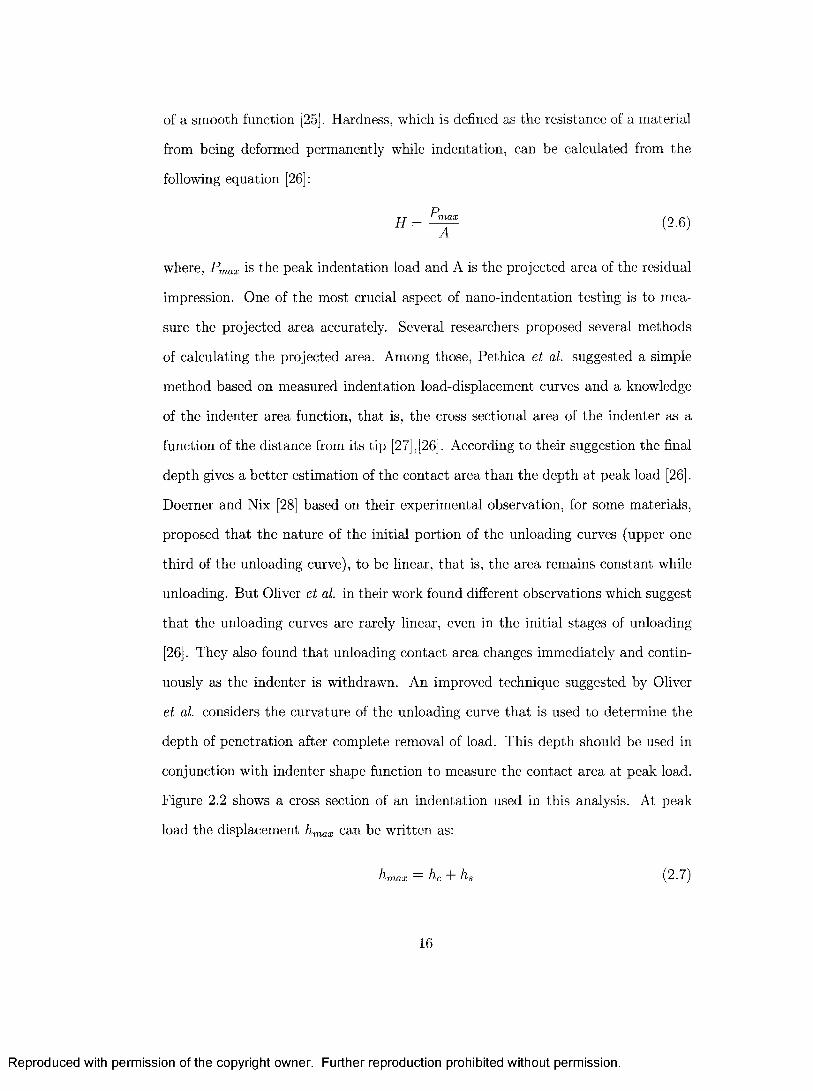
conjunction with indenter shape function to measure the contact area at peak load.
Figure 2.2 shows a cross section of an indentation used in this analysis. At peak
load the displacement hmax can be written as:
h rn a x hc T hs (2.7)
16
Reproduced with permission of the copyright owner. Further reproduction prohibited without permission.

pW C U W B L E / W B LOAD H EM OVAL.
Figure 2.2: A schematic representation o f a cross section through an indentation showing various quantities used in this analysis [26].
where, hc is the vertical distance along which contact is made and hs is the displace
ment of the surface at the perimeter of contact. The value of hmax can be measured
experimentally and hs can be obtained from the following equation [26]:
h, = (2.8)
where, S is the stiffness and Pmax is the peak load. The value of e depends upon the
geometry of the indenter. Thus, the value of hc can be calculated from the equation
(2.7). Following the assumption of Pethica et al. it is assumed th a t the projected
area of the residual impression is a function of the contact depth hc [26],
A = F (hc) (2.9)
Though over last few years most of the attention has been focused on the shape
of the unloading curves, the mechanical properties of certain materials can not be
17
Reproduced with permission of the copyright owner. Further reproduction prohibited without permission.

predicted with the help of the existing models. For many stiff hard materials and
many inhomogeneous systems the unloading curve fits no existing models particu
larly well [29]. An alternative approach is to attem pt to understand the shape of
nano-indentation loading curve [29], Hainsworth et al. formulated their model for
where, 6 is the indentation depth and 0 and V) are empirical constants. Now if either
E or H is known, then the other can be calculated from equation (2.10) [29].
2 .4 .3 F actors affectin g n a n o -in d en ta tio n te s t d a ta
The procedures tha t have been described in the previous section are associated with
various errors to measure different material properties in practice. The most serious
of these arises while measuring the depth. In addition to this, there are a number of
materials related issues tha t also affect the validity of the results. The most serious
of these are the indentation size effect (ISE) and the phenomenon of piling-up and
sinking-in [24]. In the following section some of the most commonly encountering
sources of error will be reviewed.
Initial penetration depth
In a nano-indentation test, the depth of penetration has to be measured from the
free surface of the specimen. In practice, when the indenter first makes contact with
the specimen surface with a very small initial contact load, the depth of penetration
is set to be zero. That will establish the depth reference point from which the
subsequent measurements will be obtained. This initial contact depth is usually
made to be as small as possible by applying the smallest obtainable force of the
instrument. However, no m atter how small the initial contact force is made there is
conical and pyramidal indenters and they related the load with depth of penetration
by the following equation [29]:
(2 .10)
18
Reproduced with permission of the copyright owner. Further reproduction prohibited without permission.

elastic i plastic
Figure 2.3: Schematic o f the initial penetration depth on load vs. displacement data. Pi and hi axe the initial load and displacement respectively [24].
a corresponding penetration of the indenter beneath the undisturbed specimen free
surface, as shown in Figure 2.3. To account for this small initial penetration depth,
all subsequent displacement measurements taken from the datum will be increased
by this amount. This is done by fitting the load-displacement curve to a smooth
polynomial and extrapolating to zero force. The resulting depth offset is then the
initial penetration depth and is added to all the depth reading as a correction [24].
Indentation size effect (ISE)
The indentation size effect (ISE) describes the increase in hardness by several factors
by decreasing the contact diameter or indentation depth. Based on similar hardness
increase at shallow depth in various materials, Stelmashenko et al. [30] and De
Guzman et al. [31] explained this behavior of materials in terms of a dislocation
density mechanism, Figure 2.4. The mechanism is based on the fact that, at shal
low indentation depth the geometrically necessary dislocations (those which form
in response to the imposed shape change at the surface) would form over a small
19
Reproduced with permission of the copyright owner. Further reproduction prohibited without permission.
volume, and result in a high dislocation density beneath the indenter. The high
density of dislocations hinders the movement of dislocations and thus increases the
hardness of the material. But at large penetration depth, the deformed volume over
which they are distributed becomes larger, which results in a decrease in the density
of geometrically necessary dislocations. Thus, due to low dislocation density, geo
metrically necessary dislocations have little effect on hardness at larger penetration
depth [31],[30]. They showed the expression for the hardness H in terms of the hard
ness H0 (which would be obtained without the presence of geometrically necessary
dislocations or the hardness in the absence of strain gradient):
where, h* is a length scale constant [31]. Fleck et al. [32], [33] pointed out that
indentation size effect for metals can be understood by the large strain gradient at
a small scale, which is usually omitted in conventional theories of plasticity. This
strain gradient leads to geometrically necessary dislocations tha t cause enhanced
hardness. Following this idea, Nix and Gao [34] developed a model for strain gra
dient plasticity. Later, based on some experimental observations, Gerberich et al.
[35] showed indentation size effect for several materials to be independent of in
creasing or decreasing strain gradients. They described the theory of strain gradient
to be insufficient to explain ISE at depths less than several hundred nanometers.
As an alternative model they linked ISE to a ratio between the energy of newly
created surface and plastic strain energy dissipation. For indentation depth up to
several hundred nanometers, assessment of surface work and volume work can be
fundamentally im portant feature to describe ISE [35].
Piling-up and sinking-in
In an indentation into an elastic material, the surface of the specimen is typically
drawn inwards and downwards underneath the indenter and sinking-in occurs. The
(2 .11)
20
Reproduced with permission of the copyright owner. Further reproduction prohibited without permission.

Geometrically Necessary Dislocations
Figure 2.4: Geometrically necessary dislocations created by a rigid conical indenter. Here, h is the depth o f indentation, a is the contact radius and s is the spacing between individual slip steps on the indentation surface [34].
plastic zone in this case is typically contained within the boundary of the circle of
contact and the elastic deformations th a t accommodate the volume of the indenta
tion are spread at a greater distance form the indenter. If the surface of the specimen
is forced to move outward beside the indenter then piling-up occurs. In chis case,
the plastic zone meets the surface well outside the radius of the circle of contact
[24]. The effect of piling-up and sinking-in on the contact area is shown in Figure
2.5. The existence of piling-up and sinking-in can have a detrimental effect on the
determination of the area. A correction factor can be applied to determine the con
tact area correctly. Beside the above mentioned factors, indenter geometry, surface
roughness, residual stress, thermal drift etc. also play a crucial role which affects
nano-indentation test data. Moreover, several researchers have made experimental
observations to determine the effects of tip radius [36], work hardening [37], and
surface steps [38] on nano-indentation property measurement of different materials.
21
Reproduced with permission of the copyright owner. Further reproduction prohibited without permission.

(a)
Sinking-in Piling-up
Actual contact area(b)
Indenter cross-sectional area
Figure 2.5: Effect o f sinking-in and pile-up on the actual contact area, (a)Cross- sectional view (b)plan view [24].
2.5 H ardening theories at th e nanom eter scale
Experimental results show tha t a nanolayered structure made of two kinds of metals
strengthens dramatically as the layer thickness is reduced. Several theoretical models
have been postulated based on a single dislocation gliding along one layer and many
dislocations piling up at the boundary between the layer interfaces.
2 .5 .1 O row an M odel:
Orowan model [39] states tha t while moving along the softer phase the movement of
a dislocation is blocked at the interface of the harder phase and the first deviation
from linear elastic behavior occurs when a dislocation can be curved into a semicircle
within a layer of the softer phase [9], Figure 2.6. The strength o* of the multilayers
scales with where, h is the layer thickness. As the stress rises above this point,
22
Reproduced with permission of the copyright owner. Further reproduction prohibited without permission.

4 dislocation bowing
o*°< In (hi h
Figure 2.6: Single-dislocation based Orowan model that contributes strengthening in nanoscale multilayers [40].
an increasing fraction of the load is transferred to the harder phase. The harder
phase remains elastic until it either fractures or yields [9].
2 .5 .2 H a ll-P etch M odel:
It is well known tha t the Hall-Petch equation describes the relationship between
yield strength and grain size [41]. According to this model, the yield strength scales
with the inverse square root of the relevant microstructural length scale (grain size or
interlamellar spacing or bilayer period). Since hardness scales linearly with strength
(typically, hardness is a factor of 3 higher than the flow stress) the Hall-Petch model
is also applicable in interpreting hardness increases with decreasing microstructural
length scales [40].
a = <j0 + kad~l/2 (2.12)
or
H = H0 + khd~1/2 (2.13)
23
Reproduced with permission of the copyright owner. Further reproduction prohibited without permission.
■Jl X iii.d / 2 ---------
Grain 2
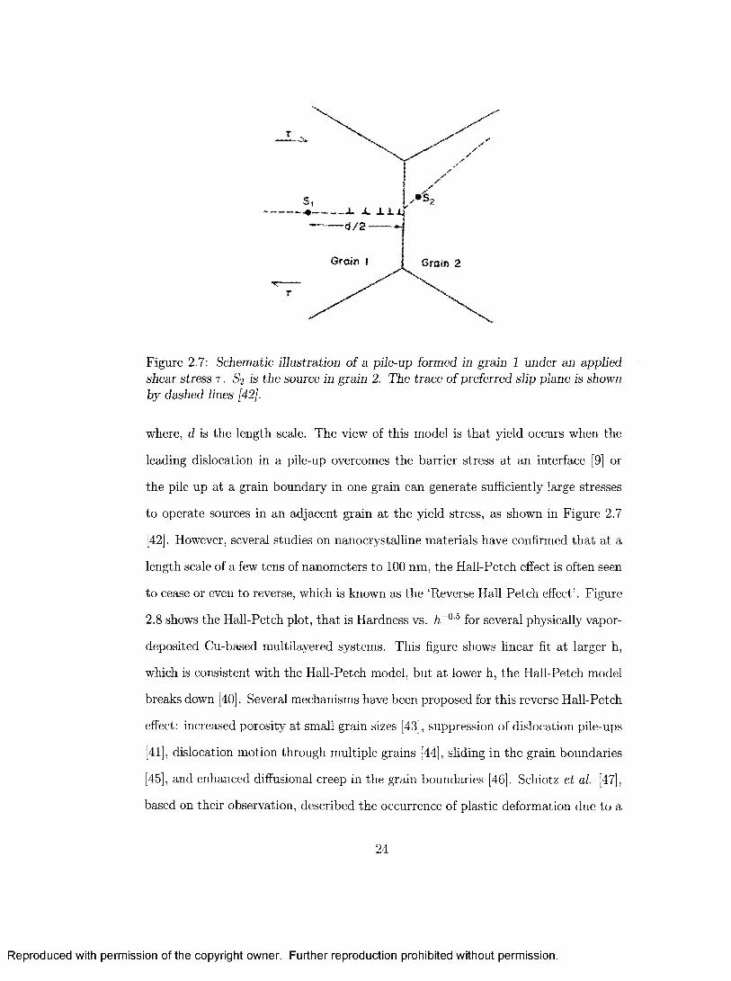
Figure 2.7: Schematic illustration o f a pile-up formed in grain 1 under an applied shear stress t . S2 is the source in grain 2. The trace o f preferred slip plane is shown by dashed lines [42].
where, d is the length scale. The view of this model is tha t yield occurs when the
leading dislocation in a pile-up overcomes the barrier stress at an interface [9] or
the pile up at a grain boundary in one grain can generate sufficiently large stresses
to operate sources in an adjacent grain at the yield stress, as shown in Figure 2.7
[42]. However, several studies on nanocrystalline materials have confirmed tha t at a
length scale of a few tens of nanometers to 100 nm, the Hall-Petch effect is often seen
to cease or even to reverse, which is known as the ‘Reverse Hall-Petch effect’. Figure
2.8 shows the Hall-Petch plot, tha t is Hardness vs. h~0,5 for several physically vapor-
deposited Cu-based multilayered systems. This figure shows linear fit at larger h,
which is consistent with the Hall-Petch model, but at lower h, the Hall-Petch model
breaks down [40]. Several mechanisms have been proposed for this reverse Hall-Petch
effect: increased porosity at small grain sizes [43], suppression of dislocation pile-ups
[41], dislocation motion through multiple grains [44], sliding in the grain boundaries
[45], and enhanced diffusional creep in the grain boundaries [46]. Schiotz et al. [47],
based on their observation, described the occurrence of plastic deformation due to a
24
Reproduced with permission of the copyright owner. Further reproduction prohibited without permission.

large number of ‘sliding’ events of atomic planes at the grain boundaries, with only
a minor part being caused by dislocation activity in the grains. Softening that they
observed was due to the larger fraction of atoms at the grain boundaries [47]. Nieh
et al. [41] proposed a grain boundary relaxation mechanism tha t could lead to a
decrease in strength at extremely fine grain sizes [41]. Based on a dislocation pile-up
model, as the grain size of the material decreases, there arrives a point at which each
individual grain will no longer be able to support more than one dislocation; at this
point the Hall-Petch relation will no longer hold. From another point of view, when
the grain size approaches zero, the material essentially becomes amorphous. The
grain boundary strengthening effect will then disappear [41], Nieh et al. calculated
the grain size based on an estimation of repulsive force per unit length between two
edge dislocations at which the strength reach a maximum value. The equilibrium
distance between two edge dislocations can be expressed as:
/c = n Gb ) H (214)7r(l — u)H
In principal when the grain size, d, is smaller than lc, there will be no dislocation
pile-ups, and the HP relation will break down [41]. The evaluation of the strength of
metallic multilayers as a function of layer thickness may be divided into four stages
[40]:
• Stage / (Hall-Petch regime). This is observed down to length scales of a few
tens of nanometers to 100 nm; a* oc /i-1/2.
• Stage II. a* oc h~a, where a ^ 0.5. This is typically observed for layer thickness
range of a few tens to a few nanometers.
• Stage III. A peak or saturation in strength is observed when the layer thickness
is a couple of to a few nanometers.
• Stage IV. Strength decreases with decreasing layer thickness, typically for h
below a couple of nanometers.
25
Reproduced with permission of the copyright owner. Further reproduction prohibited without permission.

*Cu-Cr © Cu-Nb0 Cu-Ni • Cu-Ag
fA
0 0.2.... a _!(.— . v. j... i . Lniiilmn.ni.MH t il -, i. .~l..w .....y. '.w .............. i ....... t
0.4 0.6 0.8 11N}\ (rrnT0-5)
Figure 2.8: Hall-Petch plot for several Cu-based multilayers. Linear fit (—) at larger h consistent with the Hall-Petch model. A l lower h, the Hall-Petch model (.....) breaks down [40].
Neither of these models is a complete theory of yield for multilayer systems. The
Orowan model neglects the effect of coherency and thermal expansion mismatch
stresses and it focuses on the yield of just one phase. The Hall-Petch model pays
no attention to the operation of dislocation sources [9]. Moreover, the mechanism
behind the Hall-Petch model is not directly applicable to the multilayers [19], rather
it is more applicable to the grain size effect in polycrystalline materials. In order
to improve either model, or to develop a combined model, a key requirement is to
clearly understand the barrier strength o* of the multilayer system. In order to do
this, a detailed idea about dislocation-interface interaction is necessary.
2 .5 .3 D is lo c a tio n -in ter fa ce In tera ctio n
In the classical approximation the blocking strength of an interface is attributed to
modulus mismatch, lattice param eter mismatch, chemical or gamma surface mis
match, and slip-plane mismatch between two adjacent layers. The interaction of
26
Reproduced with permission of the copyright owner. Further reproduction prohibited without permission.

dislocations with the interface due to these mismatches will be presented in the
following sections.
M odulus interaction: Im age Effect
Due to the difference in shear modulus between two adjacent layers, the strain energy
per unit length of a dislocation is generally lower in one lamella than in its neighbor,
which induces a force between a dislocation and its image in the interface. Koehler
calculated the additional stress (also known as Koehler barrier) which is required
to move a screw dislocation from a soft lamella into a hard lamella against its own
elastic image in the interface. The result is [48]:
Cn(G2 - Gx)bT = (2.15)
47r(G2 + G \)h
where, h is the distance of the dislocation from the interface, b is the Burgers vector,
and G\ and G2 are the shear modulus of adjacent layers. Since the value of r*
approaches infinity as h approaches zero, Equation (2.15) is only valid for h > 26,
i.e. it does not consider the dislocation core effects. Atomistic simulation by Rao et
al. [9] shows tha t Koehler stress is an effective barrier to dislocation motion in Cu-Ni
bilayer system, but for Cu-Ni multilayered system Koehler stress usually decreases
with wavelength of the multilayer due to the interaction of gliding dislocations with
more than one lamellar interface. Based on Peierls dislocation model, Pacheco and
Mura [49] derived the shear stress acting on the dislocation located at a distance x
from a perfectly abrupt interface, which is valid for all x including the dislocation
core:
2a(GB - G A)sm d b2 b 2xT = ------------------------------- To T x- tan — ) (2.16)7r 4x2 + 62 2x b
where, b is the magnitude of the Burger’s vector and a is A- for screw dislocation and
for edge dislocation. To compare this result with hardness data, it is necessary
to first convert the shear stress to a yield stress using Schmidt’s law, a = r /m ,
27
Reproduced with permission of the copyright owner. Further reproduction prohibited without permission.

where m is the Taylor factor, and hardness can be estimated from the yield stress
using H = 3cr [4]. Using this formula Chu and Barnett [19] showed tha t the yield
strength or hardness increases with increasing superlattice period before reaching a
saturation value for different interface width.
D islocation glide w ith in individual layers
When the layer thickness is very large, dislocations will move large distances with
out encountering an interface and will not experience significant image effects. Thus,
there must have an optimal layer thickness to inhibit dislocation motion tha t results
in maximum hardness. Sevillano [50] modelled the critical stress necessary to propa
gate dislocations within individual layers of a multilayer. According to his model, the
critical shear stress required to move a pre-existing dislocation loop that is confined
within a thin layer is given by [4]:
2aGAbsm d , t At L a = t O A + ------ ----------]n(— — ) (2.17)t A b sm 9
where, ToA is the critical shear stress required to move the dislocation loop in an
infinitely thick layer of material A. He also noted tha t if there are not sufficient
dislocations present, a larger shear stress is needed to first generate the dislocations
within the layer. This shear stress is given by [4]:
, 4aG Ab sin 9 tAt u a = t o a + ------ ----------!n( . - --) (2.18)tA 2b sm 9
Chu and Barnett [19] combined the theory by Sevillano for dislocation motion within
an individual layer with the model for image effect to obtain an overall picture of
the hardness behavior of a multilayer system. According to their model the overall
strength of a multilayer system, atot, can be expressed as:
2ab cos 0 r n , l2 \ Hi / ^1 M /&tot = o-o-\-------- t— [G2 ln (- - ) + Gi ln (- - ) (2-19)
m A b cos 9 b cos 9
where, G i° and G2° are the shear modulus of pure materials 1 and 2, A is the bilayer
period, m is the Taylor factor, b is the burgers vector. The model predictions have
28
Reproduced with permission of the copyright owner. Further reproduction prohibited without permission.

Cu/Ni: l^/A * 0.1 —• — Experimental Results
Mode) - Glide Across Layers: - 0 - -w * 2 n m - e - - w » 3 n m - & ■ - w x 4 nm
Model - Glide Within Layers:- -o- • Upper limit- -o- Lower limit
9Me
St
I
«8I
0.50 50 100 150 200
Superfatttee Period (nm)
Figure 2.9: Experimental tensile yield stress vs. superlattice period for C u/N i superlattices compared with model predictions for dislocation glide across and within layers [19].
been compared with the experimental observations for different metallic, nitride and
m etal/nitride multilayers and have shown good agreement [19],[4],[5],[2],[20],[51].
Figure 2.9 and Figure 2.10 show the comparison between the experimental results
and the model predictions for yield stress and hardness variation with superlattice
period for Cu/Ni and TiN/NbN superlattices.
Size Interaction
In multilayers, the lattice parameter mismatch between the adjacent layers is usually
taken up by misfit dislocations and coherency strain. When the lattice mismatch
is comparatively small (below the coherency wavelength limit (Ac)), then the adja
cent layers form a strained structure and the total misfit is accommodated by the
coherency strain. But larger mismatch of lattice parameters (above the coherency
wavelength limit (Ac)) relaxes the strained structure gradually, and a part of the
misfit is taken up by an array of misfit dislocations at the interface and rest of the
29
Reproduced with permission of the copyright owner. Further reproduction prohibited without permission.

<sx
JS2
Experimental Results: “ "••—TiN/NbN (paiycrysta liine) » TiN/NbN (sing le-crysta l)
Model - glide across layers:■ © • w •» 1 ,0 nm
• - w — l.S nm- 'B ■ •»( ■> z .0 nm
Model - glide within layers;- .a -upper limit- x> • - Low er limit
60
ss5045
40
35
30
25
20
1 10 100Superlattice Period (nm)
Figure 2.10: Experimental hardness vs. superlattice period for T iN /N bN superlattices compared with model predictions for dislocation glide across and within layers [19].
misfit is taken up by the coherency strain. This results in an increased density of
misfit dislocation with increasing lattice mismatch between adjacent lamellae. These
misfit dislocations act as obstacles to glide dislocation movement, at or near to the
interface. In general this barrier is expected to increase if the spacing between the
misfit dislocations decreases. The blocking strength of misfit dislocations to glide
dislocation movement can be estimated as [9]-
fo r A > Ac,(2 .20)
0 fo r A < Ac
where, ^ is the misfit of the lattice parameter, ce = 0.5, b is the Burgers vector and A
is the wavelength. Rao et al. [9] showed tha t the misfit dislocations are an effective
barrier to the glide dislocations for long wave lengths in the Cu-Ni multilayer system,
but the effect decreases gradually with multilayer wavelength.
30
Reproduced with permission of the copyright owner. Further reproduction prohibited without permission.

C hem ical Interaction
‘Chemical’ or ‘gamma surface’ mismatch between the lamellae changes the disloca
tion core energy as it approaches the interface. Both the self-energy of the dislocation
and the interaction energy between the Shockley partials continuously vary as the
dislocation moves from one lamella to next due to modulus mismatch between the
lamellae. However, the stacking fault energy changes abruptly as the leading partial
moves into the next lamella, leading to a Koehler stress as discussed before. The
chemical component of the blocking strength thus depends upon interface properties,
in this case the stacking fault energy of the interface [9].
Slip plane m ism atch
For a twinned interface where slip planes are not continuous, screw dislocations have
to cross slip for transmission of slip across the interface. As a result, the blocking
strength of such interfaces is expected to be substantially larger [9].
2.6 C om putational approach
As the field of computational material science expands, computer modeling and sim
ulation are becoming an established tool and an integral part of materials research
and design. In recent years, the advent of ever more powerful and massively parallel
computers has enabled the development of new concepts and algorithms for the com
putational modeling of materials [52]. The motivations for computer simulations of
physical systems are many fold. One of the main motivations is tha t the computer
simulation approach allows one to apply theory to study complex systems and gain
insight into their behavior. Indeed, the complexity can go far beyond the reach of
present analytical methods. There is yet another feature - computer simulations can
fill the gap between theory and experiment. Some quantities or behaviors may be
impossible or difficult to measure by experiment. W ith computer simulation such
31
Reproduced with permission of the copyright owner. Further reproduction prohibited without permission.

quantities can be computed. The laboratory experiment tells us what happens,
whereas, theory combined with computation, allows us to find out why it happens
and hopefully also to predict what will happen under similar circumstances. More
over, by comparing the results with experiment, the validity of the model can also
be ensured [53]. Other important aspects of computer simulation are the stability,
accuracy and efficiency of the solution, which are of utmost importance for solving
numerical algorithms. The explanatory, reliable and predictive capability of com
puter simulations can explain the ever-increasing impact of computation on modern
materials science [54],
2 .6 .1 A to m istic m od elin g sch em e
Atomistic simulations are playing an increasingly prominent role in materials sci
ence. At the atomic scale, defects such as dislocations, their core structures and
mechanisms of their nucleation and motion play an important role in affecting the
macroscopic material behavior. Conventional theoretical modelling and computer
simulations such as those based on continuum approaches can not reveal the effects
of such defects. Thus, those models must be supplemented with atomistic models
to characterize materials behavior [13]. Predictions resulting from this atomic-level
understanding are proving increasingly accurate and useful. Consequently, the field
of atomistic simulation is gaining ground as an indispensable partner in materials
research [12].
Interatom ic P otentials
W ith the advancement of atomistic simulations, theoretical descriptions of inter
atomic potential functions are also necessary to describe atomic interactions. In
teratomic potential functions play the most im portant role in every atomistic sim
ulation. The accuracy and complexity of the potential determine the quality of the
simulation results and the amount of computer time required [12],
32
Reproduced with permission of the copyright owner. Further reproduction prohibited without permission.
Density functional theory (DFT) is one of the earliest methods wherein simulations
were aimed towards the solution of the complex quantum many-body Schroedinger
equation of the atomic system using numerical algorithms. Though the DFT method
provides a highly accurate description of the quantum mechanical behavior of mate
rials, the system sizes are still limited to only about a few hundred atoms. Moreover,
the simulation time required is often many days of CPU time. Thus, it is essentially
impossible to compute the mechanical response of a system of realistic dimension
with this approach [55]. To get rid of this problem, physicists have developed more
approximate descriptions of the interaction between particles. These semi-empirical
models start by assuming a simplified form for the atomic interactions [56]. Substi
tution of a simpler (faster) potential allows one to obtain quick qualitative results; to
scan many cases to obtain trends; to investigate longer time scales; and to model a
larger system [12]. The simplest of such semi-empirical models is the pair potential,
where the energy, Etot of an arbitrary arrangement of N atoms is written as
Here E0 is a constant, volumetric energy, is an energy potential tha t depends
on the atomic species of both atoms i and j and riy is the distance between the i lh
and j th atoms. The pair potential is limited in its applicability, both with respect to
the materials tha t it can represent as well as the range of deformations the material
may undergo [56]. Daw et al. derived a new method, the Embedded-Atom Method
(EAM), based on density functional theory to calculate ground-state properties of
realistic metal systems [57] . In EAM, the energy is expressed as a sum of individual
atom energies and the total potential energy, E tot, of a configuration of atoms is
written as [57]
N N
(2 .21)i j^i
(2 .22 )
33
Reproduced with permission of the copyright owner. Further reproduction prohibited without permission.

In this expression, is a pair potential evaluated for the interatomic distances r^ ,
pi is the host electron density at atomic position i due to neighboring atoms, and Fj
is the embedding energy which is physically interpreted as the energy associated with
placing an isolated atom in a uniform electron gas of density pi [56]. The function
pi is found by linearly superposing the electron density from all neighboring atoms
via the expression
where pj is the spherically averaged electron density field of an isolated atom. In
this and the previous equation, the sums on j are over all atoms within some cutoff
radius, r ^ t of atom i. This cutoff generally includes the first 2 or 3 neighbor distances
in the crystal, beyond which it is assumed tha t atoms do not interact [56]. The
ground-state properties, e.g. lattice constant, elastic constants, sublimation energy
and vacancy-formation energy of the solid can be calculated from Equation (2.22)
M olecular D ynam ics (M D ) m ethod
Molecular dynamics is a popular simulation method tha t permits a computation
scale less than or equal to giga-atoms and a simulation period shorter than nano
seconds [58]. In MD simulations, a physical system of N atoms is represented by
a set of atomic coordinates, {xi\i = 1 ,2 ,..., TV} and an algorithm is used to find a
numerical solution of a set of coupled first-order ordinary differential equation, given
by the Hamiltonian formulation of Newton’s second law [13]
m il e x ' = a f ( 2'24)
where, is the mass of the i th atom and V is the interatomic potential. The
equation of motion is numerically integrated forward, with a finite time step [55].
During the simulations, the response of a material subjected to an external force is
(2.23)
[57].
34
Reproduced with permission of the copyright owner. Further reproduction prohibited without permission.
evaluated by following the dynamics of every atom in the simulation sample. The MD
simulation comprises two phases: initial relaxation and loading. In the first phase,
atoms are positioned according to an assumed lattice sites and their velocities are
randomized to satisfy the Maxwell-Boltzman distribution at prescribed temperature.
In order to reach the equilibrium state, the atoms are relaxed according to Equation
(2.24) in the absence of any external force. In the second phase, an appropriate
loading is applied by tiny increments. Thousands of relaxation steps will be engaged
after each loading increment [58].
2 .6 .2 M u ltisca le m o d e lin g schem e
It has clearly been understood tha t the materials properties are profoundly affected
by the interesting phenomena occurring at different length scales. At the atomic
(angstrom) scale, understanding of atomic interactions is necessary to character
ize materials behavior. At nanometer scale, defects such as dislocations, their core
structures and mechanisms of their nucleation and motion control the mechanical
behavior, while at scales of the micrometer or more, large collections of such de
fects including grain boundaries, dislocation pile-ups at grain boundaries and other
microstructural features, govern materials properties. However at an engineering
scale, forces arising from macroscopic stresses and/or temperature gradients may be
the controlling elements of materials performance [52]. Fully atomistic simulations
are essential for resolving the atomic scale phenomena, but they cannot be used
to model entire systems on the micrometer scale, since computations are limited
by reasonable memory requirements and simulation times. At the present state of
the art, the length scale amenable to atomistic modeling is well below the typical
grain size, which is required to model realistic microstructures [16]. In recognition
of this limitation, the field of multi-scale materials modeling has emerged, whereby
atomistic modeling is used in conjunction with larger scale models to predict the
35
Reproduced with permission of the copyright owner. Further reproduction prohibited without permission.

performance and behavior of complex materials across all relevant length and time
scales [52]. Multiscale modeling methods fall under one of the two possible cate
gories. One approach is a hierarchical scheme, wherein modeling is done separately
at different length scales and the behavior of the system at the smaller scales is
used as a source of parameters for the larger scales [16]. Such sequential model
ing approaches are usually effective when material behavior at different scales has
its own distinct characteristics [52]. The second approach is the hybrid scheme, in
which some regions of a problem are treated by a fully atomistic approach whereas
the other regions are solved by continuum approach, thus considering the material
behavior at different scales concurrently in a combined model [52]. In this section a
brief review of several methods will be presented. Detail discussion on the CADD
model, which is the focus of this thesis, will be presented in Chapter 3.
D iscrete D islocation m odeling
The Discrete Dislocation (DD) method presents a framework for solving boundary
value problems wherein dislocations are treated as continuum entities moving in
fields determined by elasticity [59], [60], [61], [62], [16]. In the DD approach, a con
tinuum problem is divided into two complementary problems, shown in Figure 2.11.
Problem I consists of dislocations in an infinite elastic continuum and is solved by
superposition of the elastic fields due to the discrete dislocations. Problem II con
sists of a linear elastic continuum writh no dislocations tha t enforces the boundary
condition across the internal boundaries. All discontinuities and singularities of the
dislocations are contained in the elastic fields due to the discrete dislocations, so the
fields of problem II, denoted as image fields, are smooth and can be solved by stan
dard numerical techniques, e.g. finite element method [14]. More detailed discussion
on the discrete dislocation method will be presented in Chapter 3. Thus, the long
range interactions between the defects are modeled accurately. The displacement
(u) and stress field (a) can be written by superposition of the two fields mentioned
36
Reproduced with permission of the copyright owner. Further reproduction prohibited without permission.

Figure 2.11: Schematic illustration o f the solution procedure o f the discrete dislocation m ethod [16].
before:
Ui = Ui + hi (2.25)
c?ij — ctij hjj (2.26)
The Q fields are the sum of the fields of the individual dislocations, in their current
configuration and the Q fields represent the image fields tha t correct for the ac
tual boundary conditions on the boundary. Short range dislocation interactions are
governed by a set of constitutive rules, for instance, the conditions required for dislo
cation nucleation, the minimum dislocation separation for annihilation, the strength
of dislocation junctions, the dislocation mobility, and dislocation/obstacle interac
tion [59], [16]. Suitable values for the parameters in these rules can be obtained
through atomistic simulations.
Q uasicontinuum (QC) m ethod
Instead of identifying atomistic and continuum region, the QC method [63],[64]
defines two types of atoms: ‘non-local representative atom s’ and ‘local representative
37
Reproduced with permission of the copyright owner. Further reproduction prohibited without permission.
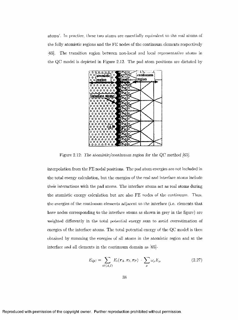
atom s’. In practice, these two atoms are essentially equivalent to the real atoms of
the fully atomistic regions and the FE nodes of the continuum elements respectively
[65]. The transition region between non-local and local representative atoms in
the QC model is depicted in Figure 2.12. The pad atom positions are dictated by
Figure 2.12: The atomistic/continuum region for the QC m ethod [65].
interpolation from the FE nodal positions. The pad atom energies are not included in
the total energy calculation, but the energies of the real and interface atoms include
their interactions with the pad atoms. The interface atoms act as real atoms during
the atomistic energy calculation but are also FE nodes of the continuum. Thus,
the energies of the continuum elements adjacent to the interface (i.e. elements tha t
have nodes corresponding to the interface atoms as shown in grey in the figure) are
weighted differently in the total potential energy sum to avoid overestimation of
energies of the interface atoms. The to tal potential energy of the QC model is then
obtained by summing the energies of all atoms in the atomistic region and at the
interface and all elements in the continuum domain as [65]-
■"IV . .1, continuum j region |
o QJUL&JL.O 1Lo0sJat»nisttcI o olmdoci ■ o 4 ilh n r r T 1} < > 0 0 0 0 0 0 0 0 J OOOOQOOI 0 0 0 0 0 0 9 0
0 0 0 0 O aSfcjDf 0 0 0 0 O 0 iiPl0 0 0 0 0 0 0 0 >0 0 0 0 0 0 01 o o o o o o o o > 0 0 0 0 0 0 0 10 0 0 0 0 0 0 8> O 0 G 0 0 0 0 » 0 0 9 0 0 0 0 0> 6 0 0 0 0 A- 0 I O o o 0 O q A P > 0 0 0 0 0 t r o >9 0 0 0 0 0 0 0 ' « 0 0 © 0 0 0 < 0 0 0 0 0 0 8 8 >0 0 0 0 0 0 81 0 0 0 0 0 9 0 0 > 0 0 0 9 0 0 O *
(2.27)
38
Reproduced with permission of the copyright owner. Further reproduction prohibited without permission.

where, the first term represents the total energy of the atomistic region by summing
the energies of the real atoms and the interface atoms [i £ (A, I)}, VA,ri,rp are
the position vectors of real, interface and pad atoms respectively, the second term
gives the total energy of the continuum region by summing the energies of individual
elements Efl in the continuum region. is the weight function and it implies that
elements tha t touch the interface contribute a fraction toM of their energy, while all
other elements contribute their entire energy to the sum. The depends on the
shape of the element, but always satisfy 0 < < 1 [65].
F inite E lem ent and A tom istic (FE A t) m ethod
The FEAt model [6 6 ], is the only model tha t attem pts to solve the problem of
a local/non-local mismatch by introducing a non-local continuum region near the
atomistic/continuum interface. The transition region for the FEAt model is shown
in Figure 2.13, where the grey elements are elements in the pad region. In the FEAt
model, the pad atoms directly overlap the continuum nodes and it extends to twice
the cut-off radius of the EAM interatomic potentials. In this way, the FE region
is resolved down to the atomic-scale in the pad region, and atoms in the atomistic
region have their full compliment of their neighbors. The FEAt model does not make
use of a unified energy function for the entire coupled problem [65]. The energy in
the elements in the FEAt model is defined in two different ways. Outside of the
pad region, non-linear elasticity is used. In an effort to mitigate the effects of the
sharp transition from a non-local atomistic region to a local continuum, the FEAt
model also uses a non-local continuum formulation to describe the energetics of the
elements in the pad region. The energy of the continuum region in the FEAt is then
found by summing the energy the local and non-local FEs [65]-
EFEAt = E Ejnonloc)(r^ rp ) + (2.28)iieP neP
39
Reproduced with permission of the copyright owner. Further reproduction prohibited without permission.

The energy of the atomistic region is found by the usual sum over atoms, including
the pad atoms, as [65]-
E F E A t = E E i(rA,r j ,r p ) (2.29)i € A, I , P
where the positions of the pad atoms provide the neighbor environment for all the
atoms in the sum.
e e a o o ■000 0 0 0 9 9 0 6 O'0 0 9 0 >00 0 0 9 0 0 0 0 0 0 0 0 9 0 >0 4 0 0 0 0 0 0 0 0 0 6 9 0 0 >0 9 0 0 0 0 0 0 9 0 9 0 0 0 0 > 0 0 9 0 9 0 9 0 9 0 0 0 0 0 0 >0 9 0 0 0 9 0 9 0 0 0 0 9 0 0 0 0 6 0 0 0 0
6 O O 0 . 6 O 0 0 >9 0 0 0 9 9 0 Q o d o o O o o
f O O O C O O C !
3 9 0 0° 3 'a to m is tic
region0 9 9 0 9 0 0 0 3 0 0 0 0 0 0o o o o c o o oiotenfc* atoms
Figure 2.13: The atomistic/continuum region for the F E A t method [65].
Concurrent L ength Scale (CLS) m ethod
In the CLS method [67], the model is designed in such a way tha t all of the pad
atoms are always in direct correspondence with nodes of finite elements in the con
tinuum region, as in the FEAt model. Also, as in the QC method, elements that
are in contact with the interface contribute less than their full energy to the total
potential energy of the system, as thus these are shaded in gray in the Figure 2.14.
In the continuum region all the finite elements are modeled as linear elastic. The
atomistic energy of the CLS method is described by the potentials with two- and
three-body interactions. Rather than considering atom-by-atom basis interactions,
the CLS method was formulated in terms of the energy of each bond in the system.
40
Reproduced with permission of the copyright owner. Further reproduction prohibited without permission.

Specifically, each two- or three-body bond contributes its full energy to the system
if all of the participating atoms in the bond are in the atomistic region or on the
interface. If the bond includes one or more atoms from the pad, the contribution is
scaled by a factor of 1/2 [65]. Examples of bonds that contribute fully (dark lines)
and partially (dash lines) are shown in Figure 2.14 [65].
sf i f to k to St & .i S..........1
o o r e g io n i — j4 » £ i“o n
O O O O t O D I Xo c o o o a o \
o a o o o o a a
> 9 0 0 0 0 0 X * X o o o a o o o a J B H K W C 1 X
> 0 0 0 0 9 0 0 \ | XE x i l e s of M l-
l o o s i i s t i (so lid ) and tM itU *> o o o o efo oo o o o o/a a o i B f s o W ? - wisht r> o o o o * » o bonds.> 0 0 0 0 * 0 0 ’f i R f f i H f l X9 9 0 0 O lo M Ds o o o o a i l a . O 9 O O O & 0 Q ) ® S H » K \ i O O O O O S D ^ v . X> 0 9 0 9 0 0 0 ...X X
Figure 2.14: The atomistic/continuum region for the CLS m ethod [65].
41
Reproduced with permission of the copyright owner. Further reproduction prohibited without permission.

Chapter 3
Coupled A tom istic and D iscrete D islocation (C A D D ) M ethod
We have discussed in the previous section tha t it is advantageous to implement mul-
tiscale modelling schemes in solving problems occurring at several length and/or
time scales, but most of the existing methods have some limitations associated with
them. For example, the FEAt method [6 6 ] and the CLS approach [67] are unable to
support continuum dislocations in the finite element region. Moreover, the size of the
atomistic region can not be easily adapted during the simulation. The quasicontin
uum (QC) method of Tadmor et al. also do not allow for the continuum description
of a dislocation, and therefore, every dislocation in the QC model requires a fully
atomistic description around its core and slip plane [16]. Hence, computational cost
becomes enormous while handling large number of dislocations. The Coupled atom
istic and discrete dislocation (CADD) model is a new hybrid scheme that extends the
capabilities of the existing models by incorporating some unique features. Like most
other existing hybrid models (i.e., FEAt [6 6 ] , CLS [67], QC method [64]), the CADD
method also begins by separating the physical problem into spatial regions tha t are
modelled either by a fully atomistic description or by continuum finite elements. But
the most unique characteristic of the CADD method is its ability to accommodate
discrete dislocations in the continuum region as well as in the atomistic region. Like
other methods the CADD model successfully reduces the computational memory
42
Reproduced with permission of the copyright owner. Further reproduction prohibited without permission.

and time from what would be required to perform the same simulations using a fully
atomistic model. Moreover, the CADD framework can detect dislocations near the
atomic/continuum interface and pass them across the interface efficiently [14],[16].
The CADD method consists of four essential components: the atomistic model, the
continuum model, the coupling between these two regions and the method for detect
ing and passing dislocations between these two regions. The first two components,
the atomistics and continuum framework, are simply taken from the well-developed
methods found in the literature. The atomistic framework is adopted from the em
bedded atom method (EAM) (see section 2.6.1) and the continuum problem can be
solved using the DD framework developed by van der Giessen and Needleman [59] as
discussed in section 2.6.2. The details of the coupling between these two regions and
the detection and passing of dislocation across the interface are the new additions
in this model [16].
A body D, shown schematically in the top left of Figure 3.1, is imagined to be di
vided into an atomistic region and a continuum region Qc joined at an interface
dQj defined by a row of atoms. The body is subjected to traction T = T 0 on c)QT
and displacement u = ito on cKlu. Since the tractions on the atomistic region are
inherently discrete, the applied load is treated as lumped forces f A on individual
atoms. The body contains N continuum dislocations, each of which has the Burgers
vector b% and position dl. where i is the number of a dislocation. The reference con
figuration is termed as X which is the undeformed, defect free state of the body and
a displacement u brings it to the deformed configuration x = X + u . This boundary
value problem is solved for the equilibrium stress cr, strain e, displacement u and
discrete dislocation positions dt in the continuum, and simultaneously for the equi
librium positions of the atoms, as a function of the imposed boundary conditions
[16]. The detail description of the solution procedures have already been published
in several journals [14],[68],[15],[16]. A brief idea about the atomistic and continuum
43
Reproduced with permission of the copyright owner. Further reproduction prohibited without permission.

solution procedure and dislocation detection and passing will be presented in the
following sections.
3.1 C ontinuum Solution Procedure
The continuum elastic problem is solved using an approach very similar to that of
the standard DD methodology described in [59]. The continuum elastic problem is
divided into two complementary problems I and II, as shown in Figure 3.1. Problem
I corresponds to an infinite homogeneous elastic material which contains N discrete
dislocations. The solution for the to tal stress ef, strain e and displacements u in
Problem I is obtained by superposition of the known elastic fields due to all the
dislocations at positions <t in an infinite elastic continuum, given by [16]
N N N
* = l = 'Y j ki> t3-1)i i i
where, er®, el and i t are the linear elastic solutions for the fields of the ith dislocation
in the infinite material. This superposition leads to tractions T along the <90-/
and some displacement u = ii along <90.u and <90/ which do not satisfy the overall
boundary conditions T0, it/ and ito. Thus, Problem II is designed as a “corrective”
boundary value problem whose fields, combined with those of Problem I, satisfy the
true boundary condition. Problem II then becomes a boundary value problem for a
linear elastic body, containing no dislocations in it. Because all the discontinuities
and singularities are associated with th e ”fields of Problem I, the fields of Problem II
are smooth and, therefore, can be solved accurately using the finite element method.
Corrective traction T = T 0 — T (on d i \ ) and corrective displacement u = v® — it
(on S0 M) and it = it/ — it (on 5 0 /) are applied as boundary conditions in this case.
The displacements, stresses, and strains of Problem II are denoted by 9 The total
fields in the continuum region are then [16]
u = u + u ) o' — d' + d’, e = e + e (3.2)
44
Reproduced with permission of the copyright owner. Further reproduction prohibited without permission.

a o r^ ! ! ||||||||||||p ^ r u
HliiiSHHir dQO • • • • • •
Ur « U
U nmU
U I
uzpad
A« + « ,
atomsI '
i I> • •
oooooooeo**••***•M IM N V
____« • • • • • • • • •••••••*«•• > 1• ••••••••• w .• • • • • • • • • 0• • • • • •
Figure 3.1: Schematic illustration o f the solution procedure for the CADD method [16].
45
Reproduced with permission of the copyright owner. Further reproduction prohibited without permission.

which satisfy the overall boundary conditions imposed on the continuum region. For
Problem II, the fully anisotropic, linear elastic constitutive relation is used, so that
the continuum elastic constants are matched those of the crystalline atomistic region.
However, for the ~ field of Problem I describing the discrete dislocations, isotropic
elasticity with the Voigt-averaged elastic constants are used. Thus the constitutive
relations in the continuum region are [16]
dij = 2 fie'ij + XekkSij (3.3)
d\j Cijkdij (3.4)
where, /j, and A are the Voigt-average elastic constants found from the fully anisotropic
modulus tensor Cijki. Thus, a fully anisotropic solution is obtained when there is
no dislocation present in the model. But when discrete dislocations exist, small er
rors are introduced due to the isotropic solution of the “field. Thus, the free energy
functional E c for the continuum region can be written as [16]
E c = i f (<r + cf) : (e + e)dV — f T o (u + u )d A (3.5)
Partial derivative of Equation 3.5 with respect to the position of the dislocation d
yields the Peach-Koehler force pl on the ith dislocation,
d E cPl = - ( ^ ) (3-6)y K d d 1 v ’
The P-K force can be obtained directly from the stress field calculated in Problems
I and II. But the finite element solution to the stress field <r, obtained at the Gauss
points of the element, is not smooth across element interfaces. Alternatively, it
is also computationally feasible to calculate the P-K force numerically during the
solution procedure [16].
46
Reproduced with permission of the copyright owner. Further reproduction prohibited without permission.

3.2 A tom istic Solution Procedure
The atomistic region is inherently non-local, since the interaction energies of realistic
interatomic potentials extend beyond-near-neighbor atoms. This region may con
tain any number of atomic defects such as dislocations, grain boundaries,vacancies,
voids, or amorphous regions. The degrees of freedom in this region are the posi
tions of the real atoms (rA) and the interface atoms ( 7 7 ). The only assumption
about these atomistic regions is that near the atomistic/continuum interface their
behavior approaches the linear elastic response used to describe the continuum. The
only nonlinear behavior allowed to “pass” across the atomistic/continuum interface
is the core of a dislocation [16]. Abruptly terminating atomistic regions, or abruptly
beginning a finite element description of the material, introduces a spurious surface
energy and non-physical interface reconstructions, as the atoms along the interface
may not have proper atomic coordination for the interatomic interactions. To over
come this problem and to ensure proper coordination of the atoms at and near the
interface, a number of pad atoms has been introduced tha t overlaps with the con
tinuum region. The pad region is shown in Figure 3.2. The pad thickness must be
such tha t real atoms can see a full complement of their neighbor atoms during the
solution process and the minimum thickness of the pad must exceed the range of
interatomic interactions rcut in the material. As the pad atoms reside on the contin
uum region, their positions are determined by interpolating the nodal displacements
obtained from the continuum solution. From the viewpoint of the real atoms and
interface atoms, the pad atom positions are instantaneously fixed. Denoting as Ei
the energy of the i th atom as determined from the EAM function, the total atomistic
free energy functional is given by [16]
E a = ^ E t(rA, T7 , rP) - f A.uA (3.7)i e{A, I ,P)
47
Reproduced with permission of the copyright owner. Further reproduction prohibited without permission.

where, ua are the atom displacements. The sum over atoms includes real atoms
(A), interface atoms (/) and pad atoms (P). Partial derivatives of E a with respect
to the positions of real atoms (r^) and interface atoms (7 7 ) then yield full atomistic
force on the atoms [16],
8 E a- W ( 3 - 8 )
The total free energy for the atomistic domain includes interactions with the pad
atoms, but partial derivatives of E a with respect to the pad atoms would generally
induce non-physical surface effects. Thus, these derivatives are simply omitted be
cause they are not needed [16]. Other than ensuring proper coordination of the real
atoms in the vicinity of the interface, the pad atoms also inform the atomistic region
about the deformation in the continuum region. Similarly, the interface atoms inform
the continuum about the deformation in the atomistic region. Due to the non-local
nature of the atoms, a finite thickness pad is required to transm it the continuum
deformation to the atoms. In contrast, because the finite element continuum is local,
only a set of interfacial atoms are required to transm it the atomistic deformation to
the continuum region.
3.3 Equilibrium configuration
After each increment of external loading it is necessary to bring the entire system
to the equilibrium. Unlike other coupling scheme (i.e. QC and CLS) CADD does
not have a well-defined energy functional for the entire system. Thus, to drive the
entire system toward equilibrium after each load step the standard, computation
ally efficient, conjugate gradient method can not be used. Alternatively, the CADD
method adopts a modified conjugate gradient minimization scheme, named Pseudo
Conjugate Gradient approach, to search for the point of zero forces on all degrees of
freedom rather than minimizing the total energy. The force values are obtained from
48
Reproduced with permission of the copyright owner. Further reproduction prohibited without permission.

the derivatives of the atomistic and continuum energy functional given in Equation
3.7 and 3.5 respectively. At the beginning of each iteration the direction of descent
is chosen using the standard conjugate gradient procedure and along this direction,
a point of zero forces is determined. At such a point, the vector of forces is per
pendicular to the direction of descent and is used to choose the direction for the
next iteration. The atomic coordinates and dislocation positions are updated during
each search step of the CG minimization. Using this revised atom and dislocation
positions, the continuum displacements and the positions of pad atoms are updated
[16],[14].
3.4 D islocation D etectio n and P assing
3.4 .1 D is lo c a tio n D e te c t io n
The key strength of the CADD approach and the feature tha t makes it unique and
powerful is its ability to detect dislocations tha t have been nucleated in the atom
istic region and tha t are moving towards the continuum region during the solution
procedure. This is done by defining a “detection band” inside the atomistic region
at a short distance from the atomistic/continuum interface, as shown in Figure 3.2.
The detection band consists of small triangular elements, with each element sitting
on three different slip planes. If a dislocation passes along one of these planes, it
generates a Lagrangian finite strain in the element of [6 8 ]
(birrij + rriibj) rriibkbkmj= 2d +
where, m is the slip plane normal, b is the burgers vector, d is the interplanar
spacing. For a given crystal structure and orientation, all the possible slip systems
and associated strains E are computed by a subroutine. The code is equipped for
FCC, Hexagonal and BCC crystals. The detection algorithm monitors the strains
in the detection band elements and compares them to all possible dislocation slip
49
Reproduced with permission of the copyright owner. Further reproduction prohibited without permission.

Plane 1
Figure 3.2: (a) Dark grey elements are used in dislocation detection. Filled circles are interface atoms and the open circles are the pad atoms that reside on the finite elements (b) A close up o f one detection element, indicating the three slip planes on which it lies [16].
strains after each CG energy minimization step. When the strain in an element
corresponds to a particular dislocation, the dislocation core is assumed to reside
at the centroid of tha t element and the slip plane and burgers vector can also be
identified [16],[68]. During the simulation many dislocations may pass through a
single detection band element. Thus, it is necessary to filter out the contributions
from all previous slip activities and consider only the displacements resulting from
new defects [6 8 ]. Moreover, the elastic deformation, rigid body translation and
rotation associated with the detection band element must also be eliminated [16].
3 .4 .2 D is lo c a tio n P a ssin g
After being detected, the dislocation is passed to the continuum as a discrete dis
location. This is done by artificially shifting the core of the dislocation along its
slip plane from its location in the detection band to a location across the interface
in the continuum region. At the same time, the continuum elastic displacement
of a dislocation dipole is superimposed onto those of the atoms and nodes. These
50
Reproduced with permission of the copyright owner. Further reproduction prohibited without permission.

( O O O O O O O O O O O O O OO O O O O O O O O O O O O O lJ O O O O O O O O O O O O O OO O O O O O O O O O O O O O L
V
(a) (b)
Figure 3.3: (a) The dislocation is detected at position x c (b) dislocation is passed across the atomistic/continuum interface at position x c + 6 [16].
displacements cancel the original core in the atomistic region at x c and replaces it
with a continuum dislocation at the position xc + 6 in the continuum region, shown
in Figure 3.3. Once this core is in the continuum region, it is added to the array
of discrete dislocations [16],[68]. While passing the dislocation from the continuum
region back to the atomistic region, it is artificially pushed into the atomistic re
gion by superposition of its linear elastic displacement fields on the atom positions.
In this case the passing is done only when the dislocation comes to within a small
tolerance of the interface. The core of the introduced dislocation is quickly relaxed
to the correct atomistic core in the subsequent energy minimization steps [16]. The
total solution procedure of the CADD method is illustrated in Figure 3.4.
The CADD method had previously been applied to examine the phenomena of
2D nano-indentation into a single crystal Aluminum film bonded to a rigid sub
strate [14]. Both thick and thin hexagonal aluminum films were studied during
3.5 M odification o f th e C A D D m odel
51
Reproduced with permission of the copyright owner. Further reproduction prohibited without permission.

Elastic Constant Crystal Structure PotentialCrystal orientation Model size and geometry
Yes No
YesLoad increment
N o
C onvergenc e
End
Applies external boundary condition
Update atomic positions
Calculate FE1VI nodal displacements Move pad atoms
Initialize FETVTCalculates and inverts stiffness matrix
Calculates new atomic positionCalculates new discrete dislocation positionsPasses dislocation
Set atomic and nodal positions Triangulation or mesh generation Calculates Burger’s vectors and dislocation data
Figure 3.4: CADD flow chart.
52
Reproduced with permission of the copyright owner. Further reproduction prohibited without permission.

displacement-controlled and force-controlled nano-indentation experiments. The
present research was started with an aim to modify the existing single grain CADD
model for multiple grains. One of our main objectives was to use this code to in
vestigate the phenomena associated with nano-indentation into a layered structure.
Two materials, i.e. Nickel and Aluminum, having distinct material properties were
selected for this present work. Nickel is characterized by its higher hardness than
aluminum, which enabled us to study a bilayered structure consists of a soft film
coated on a hard substrate and vice versa. A multilayer structure having alternat
ing layers of hard and soft materials can also be studied. The significance of such a
multilayer structure has already been discussed in Chapter 1. Moreover, the effects
of lattice constant mismatch and elastic constant mismatch between the two adja
cent layers on dislocation nucleation, dislocation movement and dislocation-interface
interaction can also be revealed.
3 .5 .1 S e lec tio n o f th e p o te n tia l
To investigate the structures and the thermodynamic properties of a system and to
obtain meaningful results from atomistic simulations of materials, the selection of
accurate potentials is of considerable interest. The usefulness of the results strongly
depends upon the quality of the interatomic potential employed in the simulation.
For metallic system, the traditional approach of using pairwise potentials have known
deficiencies to investigate the defective regions such as crack tips and free surfaces.
Daw and Baskes’s idea of adding the embedded energy term for every atom to the
pairwise potential have shown dramatic improvement in simulation results over pair
potentials without severe computational effort. Using a similar approach, Voter and
Chen [69] fit an interatomic potential to the Ni3Al alloy system. This potential can
treat fee Ni, fee A1 and the Ni3Al alloy [69]. Details of the fitting procedure are
presented in [69]. The potential gives a perfect fit to the experimental values of
53
Reproduced with permission of the copyright owner. Further reproduction prohibited without permission.

lattice constant (a0), cohesive energy (Ecoh) and bulk modulus (B) for any choice
of pair potential (*F(r)) and electron density (p(r)). Other material properties i.e.
the elastic constants, the vacancy formation energy, the bond length and the bond
energy of the diatomic molecule also show good agreement with experimental results
[69]. Figure 3.5 shows all the functions for the Ni, A1 and Ni3Al potentials. This
figure demonstrates that the repulsive nature of the embedding function is balanced
by the attractive pairwise potential and for the pure metals, the total attraction of
Ni for A1 is actually stronger than tha t of Ni for Ni or A1 for A1 [69]. Table 3.1
and Table 3.2 show the experimental data used in the fits along with the calculated
values of Voter-Chen potential for Aluminum and Nickel respectively.
3
o
t
s
ii* /
■ \ . f JL
3 4 5 e1 2r (A) p (A"3}
Figure 3.5: The functions comprising the Ni, A1 and Ni3A l potentials. The dotted lines represent the variation o f the functions with respect to scaling o f electron density (p) [69],
Indenter poten tia l
A rigid, frictionless, cylindrical indenter is chosen for indentation which is defined
by a repulsive potential of the form
* = | C (r - R ? /o r r < R ’ (3.10)| 0 fo r r > R
54
Reproduced with permission of the copyright owner. Further reproduction prohibited without permission.

Property of aluminum expt. calc.a0{A) 4.05 4.05
Ecoh{eV) 3.36 3.36B(1012erg/cm 3) 0.79 0.79
C ii( 1 0 1 2 erg /cm 3) 1.14 1.07Ci2 (1 0 1 2 er<7 /cm 3) 0.619 0.652C4 4 ( 1 0 1 2 erg /cm 3) 0.316 0.322
Vacancy formation energy A E[v (eV) 0.75 0.73Bond Energy De(eV) 1.60 1.54
Bond length R e(A ) 2.47 2.45
Table 3.1: Experimental and calculated properties o f aluminum [69].
Property of nickel expt. calc.a0(A) 3.52 3.52
Ecoh(eV) 4.45 4.45B(10X2erg/cm 3) 1.81 1.81
C n (1012 erg /cm 3) 2.47 2.44Ci2(1012erg/crri3) 1.47 1.49C4 4 (1 0 1 2 er g /cm 3) 1.25 1.26
Vacancy formation energy A E[v (eV) 1.60 1.60Bond Energy De(eV) 1.95 1.94
Bond length Re(A) 2 . 2 0 2.23
Table 3.2: Experimental and calculated properties of nickel [69]
where, C = 100eV/A2 is chosen empirically, r is the distance between atom center
and indenter center and R = 50A is chosen in this study as the indenter radius. The
A1 and Ni atoms interact with this potential , which effectively repels the atoms and
forces them to remain outside the 50A radius of the indenter.
3 .5 .2 L a ttice con stan t ca lcu la tio n for A1 and N i
For our research we selected 2D hexagonal structures of Aluminum and Nickel with
their z-axis perpendicular to the in-plane deformation. The hexagonal structure is
not a “real” crystal structure, and it is unstable both in 3D and out-of-plane defor-
55
Reproduced with permission of the copyright owner. Further reproduction prohibited without permission.

mation. It is stable in 2D because it is constrained in the z direction which allows
us to get 2D in-plane deformation. Another feature of such 2D hexagonal crystal
structure is that, a dislocation gliding on one of the three slip systems can dissociate
into two dislocations, one on each of the other two systems. Such dissociation can
be viewed as a 2D analogue to cross-slip in 3D [16]. Also, the dislocation character
can only be edge with its line direction perpendicular to the x-y plane of the model,
simplifying the details of dislocation detection and passing. Moreover, the elastic
properties are exactly isotropic in-plane for hexagonal materials. These features of
hexagonal crystal structure motivate us in using such fictitious model material for
our simulation. Our simulations cannot be used, therefore, to make accurate quan
titative predictions about real materials. Instead, they permit us to examine trends
and generic behaviors that real materials may also exhibit.
The Voter-Chen EAM potential [69] was used to create the structures of these two
materials. Initially the positions of a number of atoms for each material were gener
ated using a separate computer program. Then the structures were allowed to relax
using the molecular dynamics code (Dynamo [70]) that finds the equilibrium config
uration of the atoms using the Voter-Chen potential. The equilibrium condition to
calculate the lattice constants is given by [57]
Aij + F'(p)Vij = 0, (3.11)
where
= (3-12)m
= (3.1.3)m
and where a™ is the ith component of the position vector to the m th neighbor,
= [d$(r)/dr] r - a m and pm = [dp(r)/dr]r= a m ; (see section 2 .6 . 1 for more detail).
From the relaxed configuration of the atoms, the Bravais lattice vectors of each
56
Reproduced with permission of the copyright owner. Further reproduction prohibited without permission.

m aterial were calculated. Figure 3.6 shows the structures of these two materials
after relaxation. For Al, the Bravais vectors are:
&! = [2.7663137,0.0,0.0]
b2 = [1.383156,2.395698,0.0]
6 3 = [0.0,0.0, 3.0]
and for Ni, the Bravais vectors are:
6 1 = [2.409421,0.0,0.0]
b2 = [1.204710,2.086620,0.0]
b3 = [0 .0 , 0 .0 ,3.0]
Although, as we said earlier, the hexagonal structure is 2D and is constrained in
the z-direction, it is necessary to specify the equilibrium spacing between layers (for
hexagonal material, this is only one layer) in the z-direction to generate an infinite
crystal using DYNAMO [70]. For the DYNAMO code to work, this spacing should
be greater than half of the cutoff radius of the EAM potential. We chose the spacing
3.0.4 in the z-direction for both Al and Ni, as the cutoff radius for the Voter-Chen
EAM potential is 5.5.4. Although Al and Ni may have different independent values,
we were able to select only one periodic length in the z-direction. Thus, we had to
stretch one or compress the other along the z-direction to make them fit together.
3 .5 .3 E lastic m od u lu s C a lcu la tio n
In the CADD formulation, a fully anisotropic and linear elastic constitutive relation
is used for the "fields of Problem II, tha t describes the finite element solution of the
total continuum field, to ensure a match of elastic constants in the continuum region
to those of the crystalline atomistic region. However, for the ~ fields of Problem I
describing the discrete dislocation, we use the analytic fields from isotropic elasticity
57
Reproduced with permission of the copyright owner. Further reproduction prohibited without permission.

b,=[2.7663,0.0,0.0]30 -
2 4 6 8
40
38
37
^ 36 >
b,=[2.4094,0.0,0.0]
32
82 4 6
X(A) X(A)
(a) (b)
Figure 3.6: Bravais lattice vectors o f (a) Aluminum and (b) Nickel.
with Voigt-averaged elastic constants. The constitutive relations in the continuum
region are shown in Equation 3.3 and 3.4. The macroscopic elastic moduli Ciju in
Equation 3.4 can be written in terms of the microscopic interatomic interactions. At
equilibrium, these moduli take the form [57]
Cijki = (Bijkl + F \p )W ijkl + F '\p )V ijVkl)/£kn (3.14)
where fin is the undeformed atomic volume, and
Bijkl
WljU =m
v i3 = J 2 p ' ama? a? / arn-
(3.15)
(3.16)
(3.17)
where, <f> = [d2$ (r ) /d r2}r=an> and pm = [d2p(r)/ dr2]r=am
This expression for the elastic modulus demonstrates an im portant connection be
tween atomistic and continuum models and are used for the finite element problem.
58
Reproduced with permission of the copyright owner. Further reproduction prohibited without permission.

This expression will yield three independent non-zero components of the moduli for
a crystal with cubic symmetry. In Voigt notation they are expressed as follows [57]
C u n = Cu = [Bn + F '(p)W ll + F"(p)(Vn )2]/O 0, (3.18)
C u 2 2 = c12 = [B12 + F'(p)W 12 + F"(p)(Vn )2]/Oo, (3.19)
c1212 = c44 = [B12 + F'{p)W l2\ / n 0 , (3.20)
The materials studied in this work are hexagonal Al and Ni oriented with the z-axis
out-of-plane, so as to create an effectively 2D atomistic region. Using the Voter-Chen
EAM potential, the calculated in-plane elastic constants of aluminum and nickel are
presented in Table 3.3 and Table 3.4 respectively.
Cn = C22 1.5126 eV/A 3
C\2 = A 0.9485 eV/A 3
Cm = p 0.28203 eV/A 3
Table 3.3: Calculated in-plane elastic constants for aluminum.
Cn = C2 2 4.8722 eV/A 3
C i2 = A 2.4986 eV/A 3
Cm = P 1.1868 eV/A 3
Table 3.4: Calculated in-plane elastic constants for nickel.
3 .5 .4 M o d el d escr ip tio n for b ilayer s im u la tio n
Figure 3.7 shows a bilayer simulation model, in which a thin film of one material was
placed on top of a substrate of other material. Different film thicknesses (i.e. 40A
or 50A) were chosen for different bilayer simulation models but the overall size of
the model was kept constant at 920A by 530.4. The radius of the indenter was 50,4.
We defined one atomistic region beneath the indenter for both of these two layers.
59
Reproduced with permission of the copyright owner. Further reproduction prohibited without permission.

The thickness and the width of the atomistic region were chosen to be 160 A and
llOA respectively. To study the nucleation of the dislocations beneath the indenter,
and the interactions between the dislocations with the interface and to study the
role of misfit dislocations in the deformation process, a significant portion of the
whole system should be considered as an atomistic region under the indenter. Thus,
the width of the atomistic region is selected to be greater than the diameter of the
indenter and the thickness is chosen to be greater than the film thickness. Figure
3.8 shows the atomistic region of a 50.-4 nickel film on top of an aluminum substrate
model. The atoms are at the vertices of the small triangular elements, which are
shown only to make visualization of the deformation easier. We can also see the
interface between these two layers in the middle. Although we defined one atomistic
region for both of these two layers, the atom spacings are not uniform in the whole
region. Above the layer interface, the atoms are placed into their Bravais lattice sites
based on the lattice constant of material 1 i.e., nickel. But below the layer interface,
a new lattice constant of material 2 i.e., aluminum, is used to determine the positions
of the atoms. On the other hand, we defined several continuum regions around the
atomistic region. In these continuum regions, the size of the finite elements are set
to increase gradually as they move away from the atomistic/continuum interface,
Figure 3.9. But still the nodes of the elements represent the Bravais lattice sites
of the crystal. The last row of atoms in the atomistic region is considered as the
interface nodes between atomistic region and continuum region. After defining the
positions of the real atoms and the continuum nodes, the pad atoms are added to
the model. The pad atoms occupy the physical space of the finite elements and
their positions are determined in a similar way as for the real atoms, Figure 3.9.
The thickness of the pad region should be equal to or greater than the cut of radius
of the interatomic potentials. For the Voter-Chen interatomic potential it is 5.5A.
After creating the model, it becomes necessary to specify the materials of each atom
60
Reproduced with permission of the copyright owner. Further reproduction prohibited without permission.

200
0
> - 2 0 0
-400
-600
Top layer of thickness 40 - 50 A
Indenter of radius 50 AContinuum
Atomistic region region
Total width 920A
L__ L J I I L_J L_J L J L J I I I ! I L-500 -250 0
X(A)250 500
Figure 3.7: Bilayer simulation model.
61
Reproduced with permission of the copyright owner. Further reproduction prohibited without permission.

-50 0 50X(A)
Figure 3.8: Atomistic region under the indenter and the position o f the layer interface between Ni and Al.
and the continuum element. In the atomistic region it can be done in a straight
forward way. Any atom located above the interface are considered as material 1,
and rest of the atoms below the interface arc considered as material 2. But the
materials of the continuum elements are defined in a slightly different way. If the
centroid of an element falls above the interface then the material of tha t element
is considered as material 1 , otherwise, elements having their centroid below the
interface are considered as material 2. Although we specified a uniform thickness of
the film at the beginning, we obtained a nonuniform interface in the continuum region
as sizes of the elements increase gradually as we move further from the interface,
Figure 3.10. We assume that, this discrepancy will not introduce significant error in
our results, since it is at a very small length scale.
62
Reproduced with permission of the copyright owner. Further reproduction prohibited without permission.

•<>
-100
-120
--OOOOOOOOOOOOOOOOOOOOOOO^OOOOOO*iboooooooooooooooooooooooo^ooooo
f f i m w m m w m ®DOOOOOOOOOOOOOOOOOOOOOOOOOOOOOO 10000000000000000000000000000000 < soooooooooooooooooooooooooooooo oooo oooo oooo ooo oo
continuumatomisticinterfacepad
50 1 0 0 150
X(A)
Figure 3.9: Distribution o f real atoms (light gray circles), interface atoms (dark gray diamonds), pad atoms (white circles) and continuum nodes (black circles)in bilayer simulation model.
3 .5 .5 M o d el d escr ip tio n for m u ltilayer sim u la tion
Figure 3.11 shows the geometry of a multilayer simulation model, in which, one layer
of Ni and another layer of A1 films are placed on top of a Ni substrate. The thickness
of the films and the substrate are shown in the figure. The size of the models for
every multilayer simulation case were kept fixed at 920A by 600A. The figure also
shows the positions of the two interfaces of this model. The key feature of this model
is the addition of a second atomistic region near the second interface. An im portant
point to be noted here is the size of this region, which is little bit wider than tha t
of the first atomistic region. It is necessary to make it wider as the dislocations
nucleated in the top layers, spread out as they come down to the bottom layers. We
also made it very thin and considered only several rows of atoms on the either side
of the interface, to study the interactions between the dislocations with the interface
63
Reproduced with permission of the copyright owner. Further reproduction prohibited without permission.

Continuum region Atomistic region
-50
-100
-150 -50-200 -100X(A)
Figure 3.10: Actual position o f the interface in the continuum region (marked by dashed line), whereas, solid line defines the defined film thickness.
and with the misfit dislocations but without increasing the computational effort
significantly. It is possible to reduce the system size further by considering several
small atomistic regions along the interface, in the positions where dislocations may
interact with the interface, but tha t will increase the complexity of the modelling.
Figure 3.12 shows a close view of the positions of the real atoms, interface atoms,
pad atoms and the continuum nodes around the second interface. Here we see a
second layer of A1 film (more widely spaced atoms above the interface) is placed on
top of Ni substrate. These positions have been determined in the same way as we did
for the bilayer models. The pad atoms are also added around the atomistic region
based on the lattice constants of these two materials. As we introduced an additional
atomistic region, a second detection band is needed to be defined inside the second
atomistic region to detect the dislocations coming down from the top layers. Figure
3.13 shows the position of this second detection band inside the atomistic region.
64
Reproduced with permission of the copyright owner. Further reproduction prohibited without permission.

Indenter of 2nd Atomistic region radius 50 A 1 st Atomistic region
Layer / interfaces
tini urn reaionregior
Top film of 40 A
2nd film of 160 A
Substrate of 400 A
Total width 920 A
Figure 3.11: Multilayer simulation model.
Thereafter, a slightly different multilayer simulation model has been studied, in
which, we considered an identical multilayer simulation model as before, but ignored
the second atomistic region near the second interface. This was done intentionally by
replacing the atoms at tha t region with the continuum nodes. Thus, the gray colored
atoms in Figure 3.12 became the continuum nodes and the white colored elements
in Figure 3.13, which were initially the mesh joining those atoms, became finite
elements having different elastic constants across the interface. In brief, there was
a fully atomistic mismatch across the interface before, but only the elastic constant
mismatch after doing the modification. All other parameters, i.e. to tal number of
65
Reproduced with permission of the copyright owner. Further reproduction prohibited without permission.

-160
-180
-200
>-220
-240
-260
T O O O O O O O O O O O O O O O O O O O O O O O O O O O. o o o o o o o o o o o o o o o o o o o o o o o o o o oD O O O O O O O O O O O O O O O O O O O O O O O O O O O- o o o o o o o o o o o o o o o o o o o o o o o o o o oD O O O O O O O O O O O O O O O O O O O O O O O O O O O" O O O O O O O O O O O O O O O O O O O O O O O O O O O* ♦ ♦ ♦ ♦ ♦ ♦ ♦ ♦ ♦ ♦ ♦ ♦ ♦ ♦ ♦ ♦ ♦ ♦ ♦ ♦ 4 0 0 0 0 0 0O O O O O O O O O O O O O O O O O O O O O O O O O O O
^ ■ O O O O O O O O O O O O O O O O O O O O O O O O O O O O O O O O O O O O O O O O O O O O O O O O O O O O O O
^ O O O O O O O O O O O O O O O O O O O O O O O O O O O LO 0 0 0 0 0 0 0 0 0 0 0 0 0 0 0 0 0 0 0 0 4 0 0 0 0 0 0 OGkO OOOOOOOOOOOOOOOOO OOOOOO -O Q&p 0 0 0 0 0 0 0 0 0 0 0 0 0 0 0 0 0 ^ 0 0 0 0 0 D O O O O 0 0 0 0 0 0 0 0 0 0 0 0 0 0 0 0 4 0 0 0 0 0 0o o o o o o o o o o o o o o o o o o o o o o o o o o o
1 0 0 0 0 0 0 0 0 0 0 0 0 0 0 0 0 0 0 0 0 0 0 0 0 4 0 0 0 0 0 0 0 0 0 0 0 0 0 0 0 0 0 0 0 0 0 0 0 0 0 0 0 0 0 0 4 0 0 0 0 0 0 ^ 0 0 0 0 0 0 0 0 0 0 0 0 0 0 0 0 0 0 0 0 0 0 0 0 4 0 0 0 0 0 0 O O O O O O O O O O O O O O O O O O O O O O O O O O O o o o o > 0 ( W | ) 0 0 0 0 0 0 0 0 0 0 0 0 0 0 0 0 0 0 0 0 4 o o o o o ooopoooooooooooooooooooooooooooo1 0 0 0 0 0 0 0 0 0 0 0 0 0 0 0 0 0 0 0 0 0 0 0 0 4 0 0 0 0 0 0 3 0 0 0 0 0 0 0 0 0 0 0 0 0 0 0 0 0 0 0 0 0 0 0 4 0 0 0 0 0 0 1 0 0 0 0 0 0 0 0 0 0 0 0 0 0 0 0 0 0 0 0 0 0 0 0 4 0 0 0 0 0 0 9 0 0 0 0 0 0 0 0 0 0 0 0 0 0 0 0 0 0 0 0 0 0 0 4 0 0 0 0 0 0 ' 4 4 4 4 4 4 4 4 4 4 4 4 4 4 4 4 4 4 4 4 4 4 4 4 0 0 0 0 0 0 0e o o o o o o o o o o o o o o o o o o o o o o o o o o o o o o> 0 0 0 0 0 0 0 0 0 0 0 0 0 0 0 0 0 0 0 0 0 0 0 0 0 0 0 0 0 0 0o o o o o o o o o o o o o o o o o o o o o o o o o o o o o o oo o o o o o o o o o o o o o o o o o o o o o o o o o o o o o o
b o o o o o o o o o o o o o o o o o o o o o o o o o o o o o o> 0 0 0 0 0 0 0 0 0 0 0 0 0 0 0 0 0 0 0 0 0 0 0 0 0 0 0 0 0 0 0D O O O O O O O O O O O O O O O O O O O O O O O O O O O O O Oi£ > 0 0 0 0 0 0 0 0 0 0 0 0 0 0 0 0 0 0 0 0 0 0 0 0 0 0 0 0 0 0
_L100 125 150
X(A)
continuumatomisticinterfacepad
175
Figure 3.12: Positions o f real atoms (light gray circles), interface atoms (dark gray diamonds), pad atoms (white circles) and continuum nodes (black circles) around the second atomistic region.
the pad atoms, layer thicknesses etc., were kept constant. Our objective was to
study the change in behavior of the systems if we neglect the atomistic details in
the regions where those are im portant. Moreover, tha t also allowed us to see the
effectiveness of the continuum model to predict the dislocation behavior near the
interface compared to the atomistic model.
66
Reproduced with permission of the copyright owner. Further reproduction prohibited without permission.

170+-
-2 1 0 -
-220
-230
-240H
-25070 80 90 100 110 120 130 140 150 160
X(A)
Figure 3.13: Position o f the detection band (small black triangular elements) inside the second atomistic region. The grey elements are the continuum elements.
67
Reproduced with permission of the copyright owner. Further reproduction prohibited without permission.

Chapter 4
R esults and analysis
4.1 Bilayer sim ulation resu lts
As we have discussed in the previous chapter, the existing single grain CADD code
is modified to observe the effects of nano-indentation into an Al-Ni bilayer system.
Five different types of models are considered for bilayer simulation-
• Pure Aluminum single crystal
• Pure Nickel single crystal
• A 50A aluminum layer placed on top of a nickel substrate of 480/1 thick
• A 40/1 nickel layer placed on top of a aluminum substrate of 490.4 thick
• A 50.4 nickel layer placed on top of a aluminum substrate of 480.4 thick
In the first two cases, pure aluminum and pure nickel, are chosen as the materials
for the entire region, i.e. these are single grain calculations to establish the baseline
behavior of the pure materials. These two cases help us in determining the expected
variation of the materials’ response due to nano-indentation into bilayer systems. In
the other three cases either a nickel or aluminum layer of varying layer thickness is
placed on top of the other material.
In every model, the atoms/nodes tha t are located at the bottom surface are held fixed
68
Reproduced with permission of the copyright owner. Further reproduction prohibited without permission.

and a zero displacement boundary condition is applied. For rest of the atoms/nodes,
a zero displacement constraint is applied only in the z-direction (the deformation is
2D). The indenter is allowed to move only in the y-direction. The upper surface is
free, into which the indenter is pressed. The loading is quasi-static, and is achieved
by displacement controlled nano-indentation. In this type of loading, the indenter
position is moved down incrementally and a uniform incremental compressive strain
is superimposed on the equilibrium solution from the previous load step. Then, the
atoms, nodes, and continuum dislocations are allowed to relax while holding the
indenter at a fixed position.
4 .1 .1 A lu m in u m film on to p o f n ickel su b stra te
Aluminum has a lattice constant slightly larger than tha t of nickel. Thus, when
an aluminum film is deposited on a nickel substrate (namely Al/Ni), this mismatch
between two adjacent layers results in an array of misfit dislocations along the inter
face. Figure 4.1 shows the positions of the misfit dislocations (marked by points 1-9)
along the interface for this case. These misfit dislocations play an important role
to initiate the plastic deformation and also act as obstacles to glide the dislocation
movement, at or near to the interface. Figure 4.2 to 4.5, illustrate the deformation
phenomena occurring at the atomistic region under the indenter at various stages
of loading. The atoms are at the vertices of the small triangular elements, which
are shown only to make visualization of the deformation easier. Figure 4.2 shows a
close-up view of the misfit dislocations located at points 3-8 in Figure 4.1. As the
indentation process progresses these misfit dislocations start to move and take new
positions, points 3’-8’ in Figure 4.2, along the layer interface. An important thing
to be noticed here is tha t all these misfit dislocations move inward to the center of
the model from their initial positions while indentation progresses. At certain stage
of indentation one of these misfit dislocations (at point 6 ’ in Figure 4.2) dissociates
69
Reproduced with permission of the copyright owner. Further reproduction prohibited without permission.

2 0
0
-20
*M*V«SV.SW.M.SV.SSSSV.V.VtV.V.WtV*Vt*t«tW*V#V*V*V.V*V.*.V****MtV«V«SSW*W*VtV.V.V*V*V.V.**VtW.*#*.V.V.*#W.W*V.V.***tW#V.V|
|1tV*SV*ViSSV»VtW«V*V.W«V*4t,t*»**W*ViViV*V*****V#*«***#*t*.!*V*****‘*!#V
•W.W#V*VtV.SViV.V*SV*SV#W.»tV.*«V.,tV*#.V.W .Vt,.V*,.Vf»fVtV**.».l*ViVtV*V#,tVtV#V.V*V*V*#.**,*SVtV*VtW*Vf*t*#**V*SV*V*V.*iV*it*
****»V***V.V«V#V*V»##V.V.V***VfV***V#ifW*,*4#*#**V#V«VfSVrV.W***V*Vt»
Figure 4.1: Positions o f the mis f t dislocations (point 1-9) along the interface due to the lattice constant mismatch between A1 and Ni.
and moves into the top aluminum layer. Right after the dissociation, two disloca
tions move upward along two slip planes and reach the surface of the top layer at
point ‘A’ and ‘B’. Figure 4.3 shows the dissociation of second dislocation also from
the layer interface, point 4’ in Figure 4.3, which also travels upward along two slip
planes and reaches the top layer surface at point ‘C ’ and ‘D ’. The unique feature
of the 2D hexagonal crystal structure is that, one dislocation gliding on one of the
three slip systems can dissociates into two dislocations, one on each of the other two
70
Reproduced with permission of the copyright owner. Further reproduction prohibited without permission.

-40 -20 0 20 40 60X(A)
Figure 4.2: The primed (’) positions are the final positions o f the misfits. Dissociation of misfit starts from one of these positions (point 6’).
slip systems [14]. After reflecting back from the surface at point ‘A’, the dislocation
again dissociates into two new dislocations at point ‘E ’, Figure 4.4. One of the new
dislocations moves horizontally to the right and the other one moves down and to
the right. As the indentation process progresses further, dislocations continue to
dissociate from the layer interface and move to the aluminum layer. In addition to
the dissociation activities from the interface, some dislocations also nucleate beneath
the indenter inside the aluminum layer. But the thing to be noticed here is tha t all
of the dislocation activities i.e., nucleation, dissociation and movement are confined
within the aluminum layer instead of nickel during the whole indentation process,
Figure 4.5. Since nickel is a harder material compared to aluminum, it is easier for
a dislocation to move in aluminum than in nickel.
71
Reproduced with permission of the copyright owner. Further reproduction prohibited without permission.

-40 -20 0 20 40X(A)
Figure 4.3: Dissociation of the misfit dislocations at different locations in the layer interface.
Indenter of radius SO A
-40 -20 0 20 40X(A)
Figure 4.4: Dissociation o f dislocation (at point E) after reflecting back from the indenter surface (point A).
72
Reproduced with permission of the copyright owner. Further reproduction prohibited without permission.

-40 -20 0 „ 20 40X(A)
Figure 4.5: Accumulation o f the dislocations in the aluminum layer.
4.1 .2 N ick el film on to p o f a lu m in u m su b stra te
A similar type of response is also found when a nickel layer is placed on top of
an aluminum substrate (namely Ni/Al). Here also we notice the presence of misfit
dislocations at the interface, marked by points 1-8 in Figure 4.6. Figure 4.7 show
the initial and final positions of the misfits located between points 2-7 respectively
along the interface, which move outward from their initial positions. The opposite
motion of the misfits in this case can be explained by the presence of dislocations
of opposite sign, in Figure 4.6, to those in Figure 4.1 tha t form in the nickel layer
due to its smaller lattice constant. Moreover, the stresses induced by the indenter
also have a significant influence on the misfit dislocation movement and dissociation
along the interface, which will be discussed in the following section. As in the Al/Ni
model, one of the misfit dislocations (61) dissociates (62 and 63) and moves along
two slip planes into the lower aluminum layer. The misfit dislocation (61) in Figure
73
Reproduced with permission of the copyright owner. Further reproduction prohibited without permission.

^ - 4 0
-60
-80
-100
s jiw .'.!»:Y:*:‘i
'**.*»*.*****» s '**,*,***» s \ s s s s s s s s %****** s x$&iA4*g&% \ ' I s '*4®
* * * TT<»» * T * * * * * * * * * * * * * * * * * * * * * * *t t T T t ^ f f l T t f f T f f F f l t t t f T T V f T T T ^ “ife* *ffi*®* *®*,aT»»fe“®“da*T.*TSK»«5:*38;*i*“f]8.Tm
::;:;i::Y
sW .*.*fA_A_*.A_A
*14‘ “IS
1 1 : i i :-:s*!««*:t:«:««9i!%<j«9:«i.9:sL£»:•!>•9?*
-50 0 oX(A)
50
Figure 4.6: Position o f the misfits along N i/A l interface.
74
Reproduced with permission of the copyright owner. Further reproduction prohibited without permission.
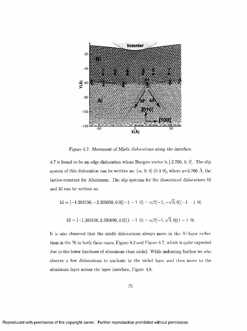
X(A)
Figure 4.7: Movement o f Misfit dislocations along the interface.
4.7 is found to be an edge dislocation whose Burgers vector is [-2.766, 0, 0]. The slip
system of this dislocation can be written as: [-a, 0, 0] (0 1 0), where a=2.766 A, the
lattice constant for Aluminum. The slip systems for the dissociated dislocations 62
and 63 can be written as:
62 = [-1 .3831 5 6 ,-2 .3 9 5 6 9 8 ,0 .0 ](-1 -1 0) = a /2 [ - l , -> /3 ,0 ](—1 - 1 0)
63 = [-1.383156,2.395698,0.0](1 - 1 0 ) = a /2 [ - l , y/3 ,0](1 - 1 0)
It is also observed tha t the misfit dislocations always move in the A1 layer rather
than in the Ni in both these cases, Figure 4.2 and Figure 4.7, which is quite expected
due to the lower hardness of aluminum than nickel. While indenting further we also
observe a few dislocations to nucleate in the nickel layer and then move to the
aluminum layer across the layer interface, Figure 4.8.
75
Reproduced with permission of the copyright owner. Further reproduction prohibited without permission.

X(A)
Figure 4.8: Passing o f dislocation across the N i/A l interface.
4 .1 .3 L oad -D isp lacem en t cu rves for A l-N i b ilayer sy s te m s
Figure 4.9 presents the variation of load-displacement curves for these five cases.
The maximum indentation depth varies from 20A to 30,4, which is approximately
50 percent of the film thickness for the bilayer models. At this large penetration
depth it is not possible to determine film properties accurately without significant
influence from the substrate. But since we are mainly interested about the dislo
cation nucleation and their interaction with the interfaces, we allow penetration as
large as possible. In every case we find a complete elastic response of the system at
the initial stage of loading, while the first drops in the curves indicate nucleation of
the first dislocations (marked by points P1-P5 in Figure 4.9). The displacement at
which nucleation occurs and the corresponding load for every case are summarized
in Table 4.1. This figure also clearly shows tha t the first dislocation nucleates at
different level of load for the different cases. Since nickel is harder than aluminum,
76
Reproduced with permission of the copyright owner. Further reproduction prohibited without permission.

>Q>
0
- J
35
30
Pure Al 50A Al layer on Ni substrate——— 40A Ni layer on Al substrate . . . . . 50A Ni layer on Al substrate ' ■ — ■ - Pure Ni
25
20
15
10
i - - / i / v i.-5
0
Displacement (A)
Figure 4.9: Load-Displacement curves for different Al-Ni bilayer system. For every case the overall thickness o f the model is 530/1.
the amount of load required to nucleate the first dislocation in nickel is much higher
than that of aluminum, see Table 4.1. Similarly a nickel layer placed on top of
an aluminum substrate also exhibit higher a load requirement to nucleate the first
dislocation compared to an aluminum layer placed top of a nickel layer.
77
Reproduced with permission of the copyright owner. Further reproduction prohibited without permission.

4 .1 .4 H ard ness m easu rem en t for b ilayer sy stem s
Load-displacement data are used to get information about the hardness variation
with indentation depth, Figure 4.10. The hardness is measured by dividing the load
by the contact area after every load step and the contact area at every load step is
calculated by taking the projected area of the indented surface. In every case the
hardness increases up to certain level of indentation depth and after that it decreases
gradually or remains constant. Before reaching the maximum hardness point, there
exist some fluctuations in the curve which have happened due to the quasi-static type
of loading and sudden increase in contact area at certain load step. The maximum
hardness obtained in each case is presented in Table 4.1. It is also clear from the
figure tha t pure nickel is the hardest among the others and the aluminum layer
placed on top of nickel shows the lowest hardness at most of the indentation depth.
Though in the Al/Ni case the bottom layer is of nickel, it still shows lower hardness
than pure aluminum. The reason can be the bottom nickel layer acts like a rigid
substrate, which impede any dislocation movement into it, thus, the overall response
of this model is almost similar to the pure aluminum except tha t the aluminum
layer thickness is less in this case. It can be concluded from this figure tha t by
placing a thin layer of hard material on a substrate of soft material dramatically
increases the overall hardness of the system and this hardness can be increased
further by increasing the layer thickness. The hardness trends after first dislocation
nucleation are shown in Figure 4.11. These trend lines are drawn only to smooth the
hardness curves tha t will make visualization easier but can not be used to predict
the materials’ response beyond the point of maximum penetration depth for each
case. According to our discussion in Chapter 2, hardening at nano-meter length scale
occurs when large number of dislocations, confined over small volume, get tangled
with each other and the movement of one dislocation is hindered by other dislocations
and also by the interface. On the other hand, the indentation size effect leads to a
78
Reproduced with permission of the copyright owner. Further reproduction prohibited without permission.

Pure Al50A Al on Ni substrate
— — 40A Ni on Al substrate - - - - 50A Ni on Al substrate PureNi
< 0.15
A y A V A 'A v ■ // ■/ 1/ '
0.05
Displacement (A)
Figure 4.10: Hardness variation with depth of penetration for different bilayer m odels. For every case the overall thickness o f the model is 530.4.
79
Reproduced with permission of the copyright owner. Further reproduction prohibited without permission.

decrease in hardness at higher penetration depth due to the lower strain gradient.
Thus, the hardness trends presented in Figure 4.11 are affected by simultaneous
contributions of these two factors. These trends suggest that the indentation size
effect is dominant in every case except for pure nickel, where the above two factors
have equal contributions. The pure aluminum model (Figure 4.11(a)) behaves like
a single crystal thick film bonded to a rigid substrate. The maximum penetration
depth (32A) is much less than its overall thickness. Thus, there is no influence from
the substrate. There exist large number of dislocations but they can spread over
a large volume. Thus, hardening due to higher dislocation density is not present.
But for an aluminum film on top of a nickel substrate model (Figure 4.11(c)), there
exists a substantial influence of the nickel substrate. Up to 20 — 25^4, hardness
decreases steadily but after that, it seems to increase with penetration depth. As
the dislocations fail to cross the Al/Ni interface, a large number of dislocations
accumulate within a small film volume and lead to increase in hardness at higher
penetration depth. However, for other two cases (Figure 4.11(d) and (e)), where
a nickel is placed on top of an aluminum substrate, even at maximum penetration
depth (which is more than 50 percent of the film thickness), dislocations are quite
mobile and do not experience any resistance from the interface. So, hardening due
to increased dislocation density or dislocation-interface interaction is not observed.
The movement of dislocations and the dissociation phenomena within single crystal
pure Ni are not so abundant as those for single crystal pure Al. Moreover, unlike
other bilayer models, the maximum indentation depth (5max) is not tha t substantial
(only 3.33 percent of the total bilayer thickness) to get any predominant effects of
one of those two factors, rather the effects of hardening is almost mitigated by the
indentation size effects at tha t small penetration depth.(Figure 4.11(b)).
80
Reproduced with permission of the copyright owner. Further reproduction prohibited without permission.

(CV/A») ssaupjBH
0.08
0.07
0.06
0.05
0.04
0.03
0.02
0.07
0.06
_ 0.05 <$ 0.04
| 0.03ax
0.02
0.01
0.00
Hardness vs. Displacement Pure Aluminum
y = 0.1151x'
10 15 20 25
Displacement (A)
0.16 i
0 .15 -T
(a)
H ardness vs. D isplacement 60AAI on Ni substrate
y = 0.1001xJ
20 30D isplacem ent (A)
0.16 -j
0.14 1
< 0.12> 0.1(0(ft 0.08»c■JJ 0.06«z 0.04
0.02
(C)
Hardness vs. Displacement Pure Nickel
0.24 y = 0.1988x0.23
0.22
j0.2
g 0.19 V«5 0 .18
0.17
12 14 16 18 20
Displacement (A)
(b)
H ardness vs. Displacement 40A Ni on Al substra te
y= 0.2552X
17 22
Displacement (A)
27
(d)
H ard n ess v s . O isp lacem ent 50A Ni on Al su b stra te
0.18 -
0.16
_ 0.14< 0.125
0.1wec 0.08■OH0.06I
0.04
0.02
o -
y = 0.4398x
13 15 17 19 21
D isp lacem en t (A)
(e)
Figure 4.11: Hardness trends after Erst dislocation nucleation for different bilayer models.
81
Reproduced with permission of the copyright owner. Further reproduction prohibited without permission.
Case S(A) P (eV /A ) Hmax{GP a)Pure Al 8.0 5.3857 10.2350A Al on top of Ni 5.8 5.3714 10.3940A Ni on top of Al 13.8 13.074 2 1 . 8 8
50A Ni on top of Al 15.3 15.333 26.13Pure Ni 1 0 . 8 24.089 37.28
Table 4.1: Summary of the results obtained from load vs. displacement curve and hardness vs. displacement curve for all bilayer models.
4 .1 .5 A to m ic level stress ca lcu la tio n
To reveal the underlying mechanisms tha t initiate the movement and dissociation
of the misfit dislocations along the interface, the atomic-level stresses are evaluated
during the indentation process. The commonly known Virial theorem is used to
evaluate these stresses, which for the EAM description of a material can be written
as
where, the superscripts I and J refer to Cartesian components, a-J refers to the stress
tensor at atom i, rJtJ is the I th component of the relative position vector between
atoms i and j , and rtj is its magnitude. Q, is the atomic volume at site i. <T>, F and p
are the pair potential, embedding energy and electron density respectively, while the
prime components denote the differentiation with respect to r*j (see section 2 .6 . 1
for more detail). Initially, when the indenter is well above the free surface, the
indenter has no effect on the stress levels of the atoms. The atomic stresses are only
the residual stresses tha t develop due to the interactions between different atoms
during the relaxation process. Figure 4.12 shows the residual stress distribution of
the atoms in the atomistic region. The interactions between Al and Ni atoms across
the interface can also be seen from this figure. When the indenter comes in contact
with the free surface, the stress levels of the atoms start to change. To get the true
82
Reproduced with permission of the copyright owner. Further reproduction prohibited without permission.

Residual stress distribution at the interface
1 0.0250 0.0224 0.0197 0.0171 0.0145 0.0118 0.0092 0.0066 0.0039 0.0013
■0.0013 - 0.0039 - 0.0066 - 0.0092 - 0.0118 - 0.0145 - 0.0171 - 0.0197 - 0.0224 - 0.0250
effect of the indenter, the residual stresses have been deducted from the total shear
stress values of every atom, ft has been found tha t during initial stages of loading,
the indenter has no significant effect on the stress levels of most of the atoms except
those located at the interface. Even when the indenter is just in contact with the
interface (depth of penetration 0.3A), it alters the stress levels of the atoms located
at the interface, Figure 4.13(a). The bright and dark colored zones in this figure
are the points where the misfit dislocation cores are located. As the indentation
83
jrrYftY
-100
[••soooiifijDoo#»»ibobi¥f 5obWi® ocoW®* ooW ffc# #ooo®®<»®®e®®®©O®®®®0OOjM®®@O@®®®®OO«*®0wuO®®®®®OO®®®e@OO®®®®OC•®®®®®®©0 ®®®®®®«®*®®©®®**®@®0 ®®®«®®0 ®®@®®®©®®®@@®®®®®@©<I I H I I I H M H I I H M I I I I M I H I H I I I M H I I I I I U I I I I I H I I t t«®®®®®®®®®e®®«®@®®@®®®®®®@®@@®®®®@®®®0 ®®t@®«®®®®®®®®«®®<»®®®®®9®®®®®®®®®®®®®®®®®®®®®®®«®®®9®9®®«®9®®««e®®«®®®®®®••••• • •••••••••••0 ® ® ® ® ® e ® e ® ® ® ® ® ® ® ® ® ® ® 0 ® ® ® ® ® ® 9 6 » ® ® ® ® ® ® ® ® <»®®®®®®®®®®®®®®®®®®®®®®®«®®®e®®®®®®®0®®®«®®®®®®®®®®®®®®®.0®0®®®®®®®®®0®®0®0®®®®09®9®®0®®0®0®®®®®0®®®®0®00®®®®®Q®<3®®®®®®®®®®®®®®0®®®®®ee®®®®®«eee®®e®e«9e®®®®®«0®®9®e®e®®
••e®®®*®®®®®®®®®®®®®®®®®®®®®®®®®®®®®®®®®®®®®®®®®®®®®®®®)i®®@®®®®®®@®®®®®««®»®@®®®«®®©®«®®®®®@®®«®®®®®®@®®®«®®§«®«®®®®®®®®®®®9®®®®®®e®e®0®®®®®®®®®®®»®®0®@®®®®®®®®®«0®®®«I®®®®®®®®®®®®®*®®®®®®®®®®®®®®*®®®®®®*®®®®®®®®®®®®®®®®®®®'•••••9® 0® ® 9® ® 9® 9® e® ® 0® ® 0«® ® ® e99e® ® ® ® ® e® ® @ ® ® ® ® ® ® 9® ® «® ® ® ® (»®®®®«®®®®9®®®®9ee®®®®®®®®®e99®®®®®®®«®®®®®®®®®®®®®®®®@®
-50 . 0 50X(A)
Figure 4.12: Residual stress distribution along the N i/A l interface.
( e V I k )
Reproduced with permission of the copyright owner. Further reproduction prohibited without permission.

”<>
-50
-100
Shear stress distribution at the interface after 3rd load step (5=0.3A)
(eV/A3)
ices;
____p .v .v .v y .v ^MtA®®®®®®®®®®®/®®®?®®®®*®®®®®®®®®®®®®®®®®®®®®®®®®®®®®® ITOMS!^AV.V.V.Y.V.V.V.V. ^ ^ ^ ^
,® ® ® ® ® ® ® ® ® ® ® #® ® #® ® ® ® ® ® ® ® ® ® ® ® ® ® ® ® ® ® © ® ® «® ® ® ® ® © ® ® ® ® ® © ® ® ® ® ® ® {
-50X(A)
50
(a)
Shear stress distribution at the interface after 18th load step (5=1.8A)
> t >r> *>po€ t
5f.V --------------- “ --------- --------W&V®V®>V®V®®'&®¥S®®«V©¥®®®@¥® ^ ®V®V®~®V®>j>® I
-100
i« Ir®®®®®®®®®®®®®®®®®®®®®®®®®®®®®®®®®®®®®®®®®®®®®®©®®®®®®®® Ii®®®®®®®®®®®®®®®®®®®®®®®®®®®®®®®®®®®®®®®®®®®®®®®®®®®®®®®* I»©©©©®®©©®«®®99®®©®9©©©a©®©©©®®®©®®®©©®®@©®®®©®®®®®®®®©© 1••••••••©©••®®®®®®®®®»®©®®®®®®®®®®©®e®®®®®©®®®®®®®®®®®®<» ® ® ® ® ® ® ® # ® ® ® ® ® ® ® ® ® ® ® ® @ ® ® ® ® ® ® ® ® ® ® ® ® @ ® ® ® ® ® ® @ ® ® ® ® @ ® ® ® ® ® © ® @ ®'•••••••••••®®®®®©®®®®®®®®®©®®®®®®®®©®®®®©©©®9®®®9®®®®®®Jg>®®®®©©®®©®®9®©©®©®©®@®®®©®@®©®©@®©@®®@®®®®®©®®®&©@®®®®®
-50 . 0 50
° i2(eV/A)
0.0250 0.0224 0.0197 0.0171 0.0145 0.0118 0.0092 0.0066 0.0039 0.0013
-0.0013 -0.0039 -0.0066 -0.0092 -0.0118 - 0.01 45 -0.0171 -0.0197 -0.0224 -0.0250
X(A)
(b)
Figure 4.13: The effect o f indenter on the atoms in the atomistic region at the indentation depth (a) 0.3.4 and (b) 1.8.4.
84
Reproduced with permission of the copyright owner. Further reproduction prohibited without permission.

progresses, the effect of the indenter at those locations on the interface becomes
more significant, Figure 4.13(b), which gradually causes the dislocations to move
along the interface and ultimately forces the dislocations to dissociate into the soft
A1 layer. The effect of the indenter on the stresses of surface atoms can also be seen
in this figure. To get a more detailed picture about this phenomenon, the stresses of
the interfacial atoms are plotted in Figure 4.14 and Figure 4.15. Figure 4.14, shows
the shear stress variation of the atoms located at the interface (Y = —50A) after
the 3rd and 18th load step. Two im portant things can be deduced from this figure.
Firstly, as the indentation process progresses the effect of the indenter becomes
Shear stress distribution at Y= - 50.0 A0.15
3rd Load step 18th Load step
0.05
000 ’0 0
Oik00,
-0.05
- 0.1-50 0 50
X(A)
Figure 4.14: Shear stress variation o f the atoms located at the interface (Y=-50.0A). The open circles are the stresses after 3rd load step and the filled circles are the stresses after 18th load step.
85
Reproduced with permission of the copyright owner. Further reproduction prohibited without permission.

0.15Shear stress distribution at Y= - 40.0 A
3rd Load step 18th Load step
• <
0.05
-0.05
- 0.1-50 500
0.15
0.1
a 0.05co(0s>£ o<o<1)■ CCO
-0.05
- 0.1 -
X(A)
(a)
Shear stress distribution at Y= - 60.0 A
3rd Load step 18th Load step
j L-50 0
X(A)50
(b)
Figure 4.15: Shear stress variation o f the atoms located (a) 10.0A above the interface (Y=-40.0A) and (b) 10.0A below the interface (Y=-60.0A). The open circles are the stresses after 3rd load step and the filled circles are the stresses after 18th load step.
86
Reproduced with permission of the copyright owner. Further reproduction prohibited without permission.

more prominent at the positions where the misfits are located. The large variation
of stresses at those positions can also be seen from this picture. Secondly, the stress
levels at the same locations on the either side of the center of the model are opposite
to each other. Though the magnitudes are not the same but the opposite nature
of the stresses results in opposite motion of the misfit dislocations along the grain
boundary. As it has been discussed before, the motion can either be inward or
outward depending upon the film-substrate system. As we move further from the
interface, either top or bottom, the effect of the indenter becomes less significant.
Figure 4.15(a) and Figure 4.15(b) show the stress variation of the atoms located
±10A from the interface. No noticeable variations are observed at those positions.
4.2 M ultilayer sim ulation results
After simulating the bilayer models, the CADD code has been modified further to
study an Al-Ni multilayer structure, and its simplest case with two layers of films
coated on a substrate is modelled. Thin layers of A1 and Ni films on either A1 or Ni
substrate are considered:
• Case I: An aluminum layer (40/4) and a nickel layer (160/4) are placed on top
of an aluminum substrate (400.4) (namely Al-Ni-A1 system).
• Case II: A nickel layer (40/1) and an aluminum layer (160/1) are placed on top
of a nickel substrate (400A)(namely Ni-Al-Ni system).
• Case III: Ni-Al-Ni system but without atomistic region at the second interface
(namely Ni-Al-Ni without 2nd atomistic).
The behavior of these models are compared with the behaviors of the pure metals
of the same model size.
87
Reproduced with permission of the copyright owner. Further reproduction prohibited without permission.

4 .2 .1 N i-A l-N i sy stem
Figure 4.16 shows the deformed configuration of the Ni-Al-Ni system due to the
nano-indentation. Any dislocation, tha t nucleates in the top Nickel film, is able to
cross the first interface quite easily, and shows easy glide along the soft aluminum
layer. But when it comes down to the second interface, its movement is blocked due
to the presence of hard Ni substrate. Moreover, the misfit dislocations present at
the interface also incorporate extra resistance to the dislocation motion. Figure 4.16
shows, one of the dislocations, nucleated in the top layer, point A in Figure 4.16,
hits one of the misfits present at the second interface, point B in Figure 4.16 and
triggers it to be dissociated into the A1 layer, point C in Figure 4.16. As we modeled
this portion of the interface with the atomistic region, both the lattice constant
mismatch and the elastic constant mismatch between adjacent layers contribute to
the blocking of dislocation movement.
4 .2 .2 N i-A l-N i sy s te m (w ith o u t an a to m istic reg ion at th e secon d in terface)
The necessity of the atomistic region near the interface can be justified by modeling
the previous case but replacing the second atomistic region with the finite elements.
Thus, we intentionally ignore the atomistic details (i.e. misfit dislocations, stacking
faults etc.) at the second interface. Figure 4.17 shows the deformed configuration
of this model due to the indentation, which is slightly different than tha t of the
previous case. As before, any dislocation tha t nucleates in the top layer can cross
the first interface very easily. But, instead of being blocked at the second interface,
it also crosses the second interface and eventually yields the hard Ni substrate,
Figure 4.17. The result suggests tha t glide dislocations do not experience significant
resistance while crossing the interface if only the elastic constant mismatch exists
between the adjacent layers. Thus, the continuum model is not sufficient to predict
88
Reproduced with permission of the copyright owner. Further reproduction prohibited without permission.

.vav ;'» w TiT;T™ »T»T»r» »T*TiT» rf*V* JV4V iV iV V iV t rtVS5 «rtTiYi ’iV j'i iTtV i -Y i'; v * w w w *v * v xvj
-100 -50 0 50 100 150
X(A)
Figure 4.16: Deformation configuration of Ni-Al-Ni model.
89
Reproduced with permission of the copyright owner. Further reproduction prohibited without permission.

-100 h
>
Indenter
-150 p
X(A)
Figure 4.17: Deformation configuration o f Ni-Al-Ni (without 2nd atomistic region) model.
the behavior exactly and requires the necessity of atomistic models at the locations
where dislocation/interface interactions are possible.
90
Reproduced with permission of the copyright owner. Further reproduction prohibited without permission.

4 .2 .3 L oad -D isp lacem en t curves for N i-A l m ultilayer sy stem s
Figure 4.18 shows a plot of load vs. displacement for all of the five cases. Like the
bilayer models, all multilayer models show a good elastic response at the initial stage
of loading. The first dislocation nucleation points are marked by points P1-P5 in
Figure 4.18 for different cases. The amount of load required to nucleate the first
dislocation (P), the corresponding penetration depth (5) and the amount of load
drop (A P), and maximum hardness obtained (Hmax) for all cases are summarized
in Table 4.2.
Pure Ni model exhibits the highest load requirement (24.869el//.4 at penetration
depth of 11.54), whereas, Al-Ni-Al models shows the lowest load requirement (4.7323el//A
at penetration depth of 6.74) to nucleate the first dislocation, which is also less than
tha t of the pure aluminum model (6.5132eH/A). The other two models, Ni-Al-Ni
and Ni-Al-Ni (without the 2nd atomistic), have almost similar P — S curves until
the first dislocation nucleates (points P2 and P3 in Figure 4.18). The amount of
load required and the indentation depth are almost the same but the amount of
load drop at those points are quite different. A higher load drop of 5.2477eV/ A in
the Ni-Al-Ni system, compared to 2.716eVj°A for Ni-Al-Ni (without 2nd atomistic)
model, corresponds to the nucleation of dislocation at the top layer, as well as the
dissociation of the misfit dislocation at the second interface. All the plastic defor
mations are confined only at the top film for Al-Ni-Al model, due to the resistance
imposed by the hard second layer at the first interface. But for the Ni-Al-Ni model,
dislocations are able to yield both the films but not the substrate. However, for
Ni-Al-Ni (without 2nd atomistic) model, the substrate has also been yielded, as the
second interface fail to block the dislocation movement.
91
Reproduced with permission of the copyright owner. Further reproduction prohibited without permission.

Load
>
Al-Ni-AlNi-Ai-NiNi-Al-Ni (without 2nd atomistic) Pure Al Pure Ni
30 /i
25
20P2
15
10P4
5
0
Displacement (A)
Figure 4.18: Load-Displacement curves for different Al-Ni multilayer system.
92
Reproduced with permission of the copyright owner. Further reproduction prohibited without permission.

4 .2 .4 H ard ness m easu rem en t for m u ltilayer sy stem s
Figure 4.19 shows the hardness vs. displacement plots for all of the multilayer
models. Pure Ni exhibits the highest hardness of 36.82 GPa (see Table 4.2) compared
to the other models. Hardness values of Ni-Al-Ni model and Ni-Al-Ni(without 2nd
atomistic) model are almost the same but less than that of the pure Ni due to the
presence of soft A1 layer in the middle. Hardness of Al-Ni-Al system is almost the
same as pure A1 since all the plastic deformations occur in the top aluminum layer.
Figure 4.20 shows the hardness trends after nucleation of first dislocation for three Al-
Ni multilayer models. For the Al-Ni-Al model, Figure 4.20(a), the hardness remains
unchanged as the indentation progresses and thus, there is no clear evidence of a
hardening or the indentation size effect. This behavior is similar to tha t obtained
in single crystal thin film results [14]. The hardness in this case is undoubtedly
affected by the close influence of a hard second layer of Ni. The hardness trend for
the Ni-Al-Ni model, Figure 4.20(b), can be said to be free from any influence of
the substrate but there exists a good influence of the interface in determining the
model’s properties. We observe a hardening effect due to dislocation blocking at the
second interface, although the rise is not very sharp. This is because the hardening
is mitigated by simultaneous indentation size effect. In the Ni-Al-Ni (without 2nd
atomistic) model, Figure 4.20(c), we do not see any dislocation blocking at any
interface, so no hardening occurs here. As such, we only see the indentation size
effect in the last model as the indentation progresses.
93
Reproduced with permission of the copyright owner. Further reproduction prohibited without permission.

Al-Ni-Al Ni-Al-Ni— - Ni-Al-Ni (without 2nd atomistic) — PureAi■ - - ■ Pure Ni ‘
0.2
0.15
><d
(0(0<Dc 0.1
nX i ' l /
0.05
•y.v
Displacement (A)
Figure 4.19: Hardness variation with depth o f penetration for different multilayer models.
Case 8(A) P (eV /A ) A P (eV /A ) Hmax(GP a) Deformed layerAl-Ni-Al 6.7 4.7323 1.3941 9.31 top film onlyNi-Al-Ni 12.3 13.559 5.2477 22.66 both of the filmsNi-Al-Ni 11.9 13.526 2.716 22.57 both films and
the substratePure A1 10.1 6.5132 0.5064 11.34 Not applicablePure Ni 11.5 24.869 2.523 36.82 Not applicable
Table 4.2: Sum mary o f the results obtained from load vs. displacement curve and hardness vs. displacement curve for all multilayer models.
94
Reproduced with permission of the copyright owner. Further reproduction prohibited without permission.

H a rd n e s s v s . D is p la c e m e n t Al-Ni-Al m o d e l
0 . 0 7
0 . 0 6
” T 0 . 0 5
% 0 . 0 4 (0 (Ag 0 . 0 3
■E 0.02
0.01
0.00
y = 0 . 0 4 4 6 X 0
5 7 9 1 1 1 3 1 5 1 7
D is p la c e m e n t (A)
(a)
H ard n ess v s . D isp lacem en tNi-Al-Ni m odel
0 . 1 6 -
0 . 1 4 -y = 0 . 0 2 1 5 x ° 507
^ 0 . 1 2 -<5 °-1 -(A8 0 . 0 8 - -- ""
<5 0 . 0 6 -X0 . 0 4
0 . 0 2
1 0 1 2 1 4 1 6 1 8 2 0 2 2 2 4
D isp lacem en t (A)
(b)
0.16
0.14
n 1?<>e 0.1(A0 08O
■o 0.06(Bz 0.04
0.02
10
Hardenss vs. Displacement Ni-Al-Ni (without 2nd Atomistic)
y = 0.1482x
******* I
12 14 16 18
Displacement (A)
(C)
20
Figure 4.20: Hardness trends after first dislocation nucleation for different multilayer models.
95
Reproduced with permission of the copyright owner. Further reproduction prohibited without permission.

C hapter 5
Conclusions and Future R ecom m endations
5.1 Sum m ary o f conclusions
Nano-crystalline metals are gaining popularity among researchers and scientists, for
both modeling and experiment, as they exhibit enhanced material properties which
are highly desirable in many engineering applications. The purpose of this work was
to investigate the underlying mechanisms and the influence of nanostructural defects
in determining the nano-indentation response and dislocation plasticity associated
with the nanolayered structures. Some interesting observations have been revealed
upon completion of this work.
We basically examined two different types of bilayer models- a soft A1 film on top
of a hard Ni substrate (Al/Ni model) and a hard Ni film on top of a soft A1 sub
strate (Ni/Al model). The behaviors of these two models were compared with the
responses of single crystal pure aluminum and pure nickel. In both of these two types
of bilayer models, the lattice constant mismatch between film and substrate led to
the formation of misfit dislocations at the layer interface. These misfit dislocations
initiated the plastic deformation and also played a key role in determining the sub
sequent overall deformation of the model. Moreover, the misfit dislocations acted
as obstacles to the glide dislocation movement. During the indentation process, the
96
Reproduced with permission of the copyright owner. Further reproduction prohibited without permission.

movements of misfit dislocations were observed along the layer interface, either in
ward or outward of the center of the model, depending upon the placement of the
material in the layers. Dissociation of the misfit dislocations, which can be viewed
as a 2D analogue of cross-slip in 3D, occurred from the interface at certain stage of
indentation, and in every bilayer model it happened into the aluminum layer (either
film or substrate) due to its lower hardness compared to nickel. It had also been
revealed that the stress field induced by the indenter dictated the movement of the
misfit dislocations along the interface and their dissociations. When the indenter
was brought in contact to the surface, it significantly altered the stress level of the
atoms tha t were located near the surface and along the interface. The effect was
found to be more intense especially at the locations where the misfit dislocations
were located. However, the stress field of the indenter did not significantly affect the
stress levels of the atoms tha t were located away from the surface or the interface.
Load -displacement curves for each bilayer model showed good elastic response of
the model at the initial stages of loading, whereas, the first drop in each curve was an
indication of the initiation of plastic deformation of the models either by nucleation
of a dislocation or by dissociation of a misfit dislocation from the interface. This
phenomenon occurred at different level of load and different indentation depth for
every case. Pure nickel was found to exhibit a higher load requirement than pure
aluminum to nucleate the first dislocation. Similarly, the Ni/Al model exhibited a
higher load requirement to initiate the dissociation of a misfit dislocation than the
Al/Ni bilayer model. The variation of hardness with indentation depth was mea
sured by dividing the load by the projected contact area after every load step. It
was found tha t the overall hardness of the bilayer models depend primarily upon
the hardness of the film, although at higher penetration depths, the substrate ef
fect cannot be ignored. Thus, by placing a hard film coating on a soft substrate
enhanced the hardness and further enhancement was achieved by increasing the film
97
Reproduced with permission of the copyright owner. Further reproduction prohibited without permission.

thickness. The hardness trends after the first dislocation nucleation were dictated by
simultaneous contributions from the indentation size effect due to the strain gradi
ents and the hardening effect due to the high dislocation density. The hard substrate
exhibited substantial resistance to dislocation movement and resulted in hardening
when penetration depth was more than 50 percent of the film thickness. On the
other hand, the soft substrate failed to resist dislocation movement and did not
show any hardening effect even at a large penetration depth as the substrate also
yielded along with the film. The responses of the pure materials were believed to be
free from any effects of the substrate since the maximum indentation depths were
very small compared to the overall film thickness. Easy glide of dislocations and
dissociation events within pure aluminum resulted in lower dislocation density and
indentation size effect at higher indentation depth. Whereas, the indentation size
effect was almost mitigated by the effect of hardening due to the lack of dislocation
movements and scarce dissociation events within single crystal pure nickel.
The multilayer models were constructed by placing two layers of film on top of a
substrate, for example, A1 and Ni films on top of A1 substrate (Al-Ni-Al model) and
Ni and A1 films on top of Ni substrate (Ni-Al-Ni model). An additional atomistic
region was introduced in each of these two models to consider the full atomistic
details (i.e. misfit dislocation, staking faults etc.) at the second interface. The
necessity of this atomistic region was validated by constructing a third model, in
which the second atomistic region was replaced by a continuum region (Ni-Al-Ni
without 2nd atomistic model), to see the effectiveness of the continuum models to
elucidate the phenomena of dislocation-interface interactions at the second inter
face. Load-displacement plots for all multilayer models also exhibited good elastic
response of the models before initiation of any plastic deformation. The Ni-Al-Ni
model and Ni-Al-Ni without second atomistic model had almost the same response
upto the points of first dislocation nucleation, but the amount of load drops at those
98
Reproduced with permission of the copyright owner. Further reproduction prohibited without permission.

points were different in these two cases. The higher load drop in the first model was
attributed to the blocking of dislocations coming down from the top layers at the
second interface and simultaneous dissociation event of a misfit dislocation from this
interface. While in the second model, continuum description at the second interface
failed to capture the picture accurately as dislocations coming down from the top
layers were able to pass the interface quite easily and also yielded the substrate. The
hardness trends after the first dislocation nucleation also exhibited their dependence
upon simultaneous contributions from the indentation size effect and the hardening
effect due to the high dislocation density. In the Ni-Al-Ni model, a hardening effect
due to dislocation blocking was clearly seen, which mitigated the indentation size
effect a t a large penetration depth. On the other hand, this hardening effect was
absent when atomistic details at the interface were ignored. Rather, gradual soften
ing of the model indicated easy glide of the dislocations through the films and the
substrate.
5.2 R ecom m endations for future work
There exist a range of possible extensions of the present study to get further insight
into the indentation response of the nanolayered structures.
• A major im portant direction for future work is to extend the CADD method
to a 3D formulation. T hat will require implementation of a parallel computing
framework, but tha t will facilitate the investigation of real crystal structures
(fee, bcc, hep etc.). In the 3D CADD framework, handling of dislocation loops
wholly contained either in the atomistic region or in the continuum region may
not be a problem but the major challenge will be in handling single dislocation
loops located partly in the atomistic region and partly in the continuum region.
• The effect of different crystal orientations in different layers on the indenta-
99
Reproduced with permission of the copyright owner. Further reproduction prohibited without permission.

tion response should also be studied. In this present study, the same crystal
orientation (100) was considered for each layer. Thus, the dislocations did not
experience any resistance due to the slip plane mismatch while crossing the
interface. But, it is a well known fact tha t materials possess different proper
ties in different directions and their behaviors also vary tremendously with the
change of the crystal orientation. Thus, modeling different crystal orientations
for different layers will facilitate to reveal the effects of slip plane mismatches
on dislocation movement across the interface in addition to the lattice con
stant mismatch and elastic constant mismatch. It is strongly believed tha t by
selecting the crystal orientation properly in each layer, it is possible to create
structures having properties even better than tha t of any of the constituent
materials.
• It is also necessary to investigate the behavior of other metallic systems in
volving copper, silver, gold etc. Appropriate interatomic potentials for ternary
systems may help to study models consisting of three different materials. Cur
rently, work is being progressing using the EAM interatomic potential for alu
minum, silver and copper developed by C.L. Rohrer [71]. This potential will
allow us to create bilayer structures involving Al-Cu, Al-Ag and Ag-Cu and
multilayered structures involving alternating layers of Al, Ag and Cu. Many
interesting observations may come out upon revealing the properties associated
with these materials. However, metal-nitride systems or nitride-nitride systems
will require extensive modification of the existing CADD code and selection of
appropriate interatomic potentials. This is because covalently bonded nitrides
require higher order potentials.
• Dislocation nucleation and movement in the atomic and continuum regions
during the unloading cycle can be analyzed to complete the indentation experi-
100
Reproduced with permission of the copyright owner. Further reproduction prohibited without permission.

ment. Previous study of nano-indentation on single crystal aluminum revealed
some interesting observations including dislocation nucleation, annihilation,
pile-up of materials and a ‘Bauschinger’ effect due to the reverse motion of the
pre-existing dislocations upon removal of the load. In addition to these, the
role of misfit dislocations and the interfaces in this reverse plasticity can be
revealed upon completion of the unloading modeling of the layered structures.
Moreover, to determine the stiffness and modulus of the layered structures it
is necessary to analyze the unloading part of the load-displacement curves.
• To get a more realistic picture and to compare the results with experimental
observations, it is necessary to increase the number of layers of the models.
Typical multilayer coating structures are not limited to one or two layers of
film on a substrate; sometimes they may consist of up to hundreds of layers.
Moreover, the layer thickness should also be reduced, since most of the mul
tilayer structures exhibit substantial strength and hardness enhancement at a
bilayer period between 10~20 A. Defining separate atomistic region for each
interface will definitely increase the complexity of the modeling. Instead, a
single atomistic region can be constructed tha t will include all the interfaces.
But handling this gigantic atomistic region in a single processor will require
several days or even months computational time to solve one single problem. A
parallel version of the CADD method is thus necessary to save computational
time and to handle large number of atoms and nodes.
These proposed studies will help to reveal the potential to create a new class of
high strength materials and will be a contribution towards further understanding of
im portant aspects of materials science through computer simulation of deformation
mechanisms in crystalline solids.
101
Reproduced with permission of the copyright owner. Further reproduction prohibited without permission.

Bibliography
[1] D.E. Kramer, M.F. Savage, A. Lin, and T. Foecke. Novel method for TEM
charcterization of deformation under nanoindents in nanolayered materials.
Scripta Materialia, 50(6):745-749, 2004.
[2] S.A. Barnett and A. Madan. Hardness and stability of metal-nitride nanoscale
multilayers. Scripta Materialia, 50(6):739-744, 2004.
[3] I.A. Ovid’ko. Deformation of nanostructures. Science, 295(5564):2386, 2002.
[4] P.C. Yashar and W.D. Sproul. Nanometer scale multilayered hard coatings.
Vacuum, 55:179-190, 1999.
[5] Q. Yang, C. He, L.R. Zhao, and J-P. Immarigeon. Preferred orientation and
hardness enhancement of TiN/CrN superlattice coatings deposited by reactive
magnetron sputtering. Scripta Materialia, 46:293-297, 2002.
[6] Z. Shan, E.A. Stach, J.M. Wiezorek, J.A. Knapp, D.M. Follstaedt, and S.X.
Mao. Grain boundary-mediated plasticity in nano crystalline nickel. Science,
305(5684) :654-657, 2004.
[7] K.W. Jacobsen and J. Sciotz. Computational material science: Nanoscale plas
ticity. Nature Materials, pages 15-16, 2002.
[8] D. Saraev and R.E. Miller. Enhanced hardness of copper crystals by nanometer
sized nickel coatings, subm itted to Acta Mat., 2005.
102
Reproduced with permission of the copyright owner. Further reproduction prohibited without permission.

[9] S.I. Rao and P.M. Hazzledine. Atomistic simulation of dislocation-interface
interactions in the Cu-Ni multilayer system. Phil. Mag. A, 80(9):2011-2040,
2000 .
[10] Y.M. Wang, M.W. Chen, F.H. Zhou, and E. Ma. High tensile ductility in a
nanostructured metal. Nature, 419:912-915, 2002.
[11] R.Z. Valiev, I.V. Alexandrov, Y.T. Zhu, and T.C. Lowe. Paradox of strength
and ductility in metals processed by severe plastic deformation. J. Mater. Res.,
17(1), 2002.
[12] A.F. Voter. Inter atomic potentials for atomistic simulation. M RS bulletin,
pages 17-19, 1996.
[13] A. Nakano, M.E. Bachlechner, T.J. Campbell, R.K. Kalia, A. Omeltchenko,
K. Tsuruta, and P. Vashishta. Atomistic simulation of nanostructured materials.
IEEE computational science and engineering, 5(4):68-78, 1998.
[14] R.E. Miller, W.A. Curtin, and L.E. Shilkrot. A coupled atomistics and discrete
dislocation plasticity simulation nano indentation into single crystal thin films.
Acta Mat., 52(2):271-284, 2004.
[15] L.E. Shilkrot, R.E. Miller, and W.A. Curtin. Coupled atomistic and discrete
dislocation plasticity. Phys. Rev. Lett., 89(2):025501/l-025501/4, 2002.
[16] L.E. Shilkrot, R.E. Miller, and W.A. Curtin. Multiscale plasticity modeling:
Coupled atomistic and discrete dislocation mechanics, submitted to J. Mech.
Phys. Sol., 2003.
[17] Milton Ohring. The Materials Scinece of Thin Films. Academic Press, INC,
San Diego, CA, 1992.
103
Reproduced with permission of the copyright owner. Further reproduction prohibited without permission.

[18] R.C. Cammarata and T.E. Schlesinger. Nanoindentation study of the me
chanical properties of copper-nickel multilayered thin films. Appl. Phys. Lett.,
56(19):1862-1863, 1990.
[19] Xi Chu and Scott A. Barnett. Model of superlattice yield stress and hardness
enhancement. J. Appl. Phys., 77(9):4403-4411, 1995.
[20] P.B. Mirkarimi, L. Hultman, and S.A. Barnett. Enhanced hardness in
lattice-matched single-crystal TiN/Vo.gNbo^N superlattice. Appl. Phys. Lett.,
57(25) :2654-2656, 1990.
[21] Thin Films. American Society for Metals, Ohio, 1964.
[22] R.A. Coombe, editor. The Electrical Properties and Applications of Thin Films.
Sir Issac Pitm an and Sons Ltd., London, 1967.
[23] L.I. Maissel and M.H. Francombe. An Introduction to thin films. Gordon and
Breach, New York, N.Y., 1973.
[24] Anthony C. Fischer-Cripps. Nanoindentation. Springer, second edition, 2004.
[25] G.M. Pharr, W.C. Oliver, and F.R. Brotzen. On the generality of the re
lationship among contact stiffness, contact area, and elastic modulus during
indentation. J. Mater. Res., 7(3):613—617, 1992.
[26] W.C. Oliver and G.M. Pharr. An improved technique for determining hardness
and elastic modulus using load and displacement sensing indentation experi
ment. J. Mater. Res., 7(6): 1564-1580, 1992.
[27] J. B. Pethica, R. Hutchings, and W. C. Oliver. Hardness measurements at
penetration depths as small as 20 nm. Phil. Mag. A, 48(4):593-606, 1983.
[28] M.F. Doerner and W.D. Nix. A method for interpreting the data from depth-
sensing indentation instruments. J. Mater. Res., l(4):601-609, 1986.
104
Reproduced with permission of the copyright owner. Further reproduction prohibited without permission.

[29] S.V. Hainsworth, H.W. Chandler, and T.F. page. Analysis of nanoindentation
load-displacement loading curves. J. Mater. Res., 11 (8): 1987-1995, 1996.
[30] N.A. Stelmashenko, M.G. Walls, M.L.Brown, and Y.V. Milman. Microinden
tations on W and Mo oriented single crystals: An STM study. Acta Melall.
Mater., 41 (1):2855-2865, 1993.
[31] M.S. De Guzman, G. Neubauer, P. Flinn, and W.D. Nix. The role of indentation
depth on the measured hardness of materials. Mat. Res. Soc. Symp. Proc.,
308:613-618, 1993.
[32] N. A. Fleck, G. M. Muller, M. F. Ashby, and J. W. Hutchinson. Strain gradient
plasticity: Theory and experiment. Acta Met. et Mat., 42:475-487, 1994.
[33] N. A. Fleck and J. W. Hutchinson. Strain gradient plasticity. Adv. in Appl.
Mech., 33:295-361, 1996.
[34] W.D. Nix and H. Gao. Indentaion size effects in crystalline materials: A law
for strain gradient plasticity. J. Mech. Phys. Sol, 46(3):411-425, 1998.
[35] W.W. Gerberich, N.I. Tymiak, J.C. Grunlan, M.F. Horstemeyer, and M.I.
Baskes. Interpretation of indentation size effects. J. Appl. Mech., 69:433-442,
2002 .
[36] Chung-Jen Lu and D.B. Bogy. The effect of tip radius on nano-indentation
hardness tests. Int. J. Sol. and Struc., 32(12):1759-1770, 1995.
[37] Yo-Han Yoo, Woong Lee, and Hyunho Shin. Effect of work hardening on the
critical indentation limit in spherical nano-indentation of thin film /substrate
systems. Surface and coatings technology, 179:324-332, 2004.
[38] J.A. Zimmerman, C.L. Kelchne, P.A. Klein, J.C. Hamilton, and S.M. Foiles.
Surface step effects on nanoindentation. Phys. Rev. Lett., 87(16), 2001.
105
Reproduced with permission of the copyright owner. Further reproduction prohibited without permission.
[39] J.D . Embury and J.P. Hirth. On dislocation storage and the mechanical re
sponse of fine scale microstructures. Acta. Metall. Mater., 42:2051, 1994.
[40] A. Misra, J.P. Hirth, and H. Kung. Single-dislocation-based strengthening
mechanisms in nanoscale multilayers. Phil. Mag. A, 82( 16):2935 2951, 2002.
[41] T.G. Nieh and J. Wadsworth. Hall-petch relation in nanocrystallinc solids.
Scripta Metallurgica, 25:955-958, 1991.
[42] D. Hull and D.J. Bacon. Introduction to Dislocation. Springer, third edition,
1984.
[43] R.W. Siegel and G.E. Fougere. Nanophase Materials: Synthesis-Properties-
Application. NATO-ASI Ser. E, Vol 260, Kluwer, Dordrecht, 1994.
[44] J. Lian, B. Baudelet, and A.A. Nazarov. Model for the prediction of the me
chanical behaviour of nanocrystalline materials. Mater. Sci. Eng. A, 172:23-29,
1993.
[45] T. G. Langdon. The significance of grain boundaries in the flow of polycrys
talline materials. Mater. Sci. Forum, 189-190:31-42, 1995.
[46] A.H. Chokshi, A. Rosen, J. Karch, and H. Gleiter. On the validity of the hall-
petch relationship in nanocrystalline materials. Scripta Materialia, 23:1679-
1684, 1989.
[47] J. Schiotz, Francesco D. Di Tolla, and K.W. Jacobsen. Softening of nanocrys
talline metals at very small grain sizes. Nature, 391:561-563, 1998.
[48] J.S. Koehler. Attempt to design a strong solid. Phys. Rev. B, 2(2):547—551,
1970.
[49] E.S. Pacheco and T. Mura. Interaction between a screw dislocation and a
bimetallic interface. J. Mech. Phys. Sol., 17:163-170, 1969.
106
Reproduced with permission of the copyright owner. Further reproduction prohibited without permission.

[50] J.G. Sevillano. Strength of metals and alloys. Perganom, Oxford, 1980.
[51] U. Helmersson, S. Todorova, S. A. Barnett, and J.E. Sundgren. Growth of single
crystal TiN/VN strained-layer superlattices with extremely high mechanical
hardness. J. Appl. Phys., 62(2):481-484, 1987.
[52] T.D. de la Rubia and V.V. Bulatov. Materials research by means of multiscale
computer simulation. M RS bulletin, pages 169-170, 2001.
[53] Dieter W. Heermann. Computer simulation method. Springer-Verlag, Germany,
1986.
[54] J. Hafner. Atomic-scale computational materials science. Acta Mat., 48:71-92,
2000 .
[55] D. Srivastava and S.N. Atluri. Computational nanotechnology: A current per
spective. CMES, 3(5):531-538, 2002.
[56] Ronald E. Miller. On the generalization of continuum models to include atom
istic features. PhD thesis, Brown University, 1998.
[57] M. S. Daw and M. I. Baskes. Embedded-atom method: Derivation and ap
plication to impurities, surfaces, and other defects in metals. Phys. Rev. B,
29:6443-6453, 1984.
[58] MA Xinling and Yang Wei. MD simulation for nanocrystals. Acta Mechanica
Sinca, 19(6):485-507, 2003.
[59] A. Needleman and E. Van der Giessen. Discrete dislocation plasticity. Key
Engineering Materials, 233-236:13-24, 2003.
[60] E. Van der Giessen and A. Needleman. Discrete dislocation plasticity: a simple
planar model. Model. Simul. Mater. Sci. Eng., 3:689-735, 1995.
107
Reproduced with permission of the copyright owner. Further reproduction prohibited without permission.

[61] L.P. Kubin and G. Canova. The modelling of dislocation patterns. Scripta
Metallurgica, 27:957-962, 1992.
[62] Hussein M. Zbib, Moono Rhee, and John P. Hirth. On plastic deformation and
the dynamics of 3D dislocations. Int. J. Mech. Sci., 40(2-3): 113-127, 1998.
[63] R.E. Miller and E.B. Tadmor. The quasicontinuum method: Overview, appli
cations and current directions. J. Comp. Aid. Mat. Des., 9:203-239, 2002.
[64] E. B. Tadmor, M. Ortiz, and R. Phillips. Quasicontinuum analysis of defects
in solids. Phil. Mag. A, 73(6): 1529-1563, 1996.
[65] W.A. Curtin and Ronald E. Miller. Atomistic/continuum coupling in compu
tational material science. Mod. Simul. Mater. Sci. Eng., 11:R33-R68, 2003.
[6 6 ] S. Kohlhoff, P. Gumbsch, and H. F. Fischmeister. Crack propagation in bcc
crystals studied with a combined finite-element and atomistic model. Phil.
Mag. A, 64(4):851-878, 1991.
[67] J.Q. Broughton, F.F. Abraham, N. Bernstein, and E. Kaxiras. Concurrent
coupling of length scales: methodology and application. Phys. Rev. B, 60:2391-
2403.
[6 8 ] Ronald E. Miller. Direct coupling of atomistic and continuum mechanics in
computational material science. International Journal for Multiscale Computa
tional Engineering, 1 (1) :57—72, 2003.
[69] A.F. Voter and S.P. Chen. Accurate interatomic potentials for Ni, A1 and M 3 AI.
Mat. Res. Soc. Symp. Proc., 82:175-180, 1987.
[70] M. S. Daw and S. M. Foiles. Dynamo version 8.7. FORTRAN code, 1994.
[71] C. L. Rohrer. Interatomic potentials for Al-Cu-Ag solid-solutions. Modeling
Simul. Mater. Sci. Eng., 2:119-134, 1994.
108
Reproduced with permission of the copyright owner. Further reproduction prohibited without permission.