multiple output lvds - q-tech corporation€¦ · 5.3.2 mil-std-750, test methods for semiconductor...
TRANSCRIPT
Q-TECH Corporation - 10150 W. Jefferson Boulevard, Culver City 90232 - Tel: 310-836-7900 - Fax: 310-836-2157 - www.q-tech.com
MULTIPLE OUTPUT LVDS SERIES3.3Vdc, 1 to 12 Differential LVDS Pairs, Space Qualified Crystal Oscillators
15MHz to 200MHzQ-TECHCORPORATION
QPDS-0115 Rev. E - August 2017 1 of 18
Description
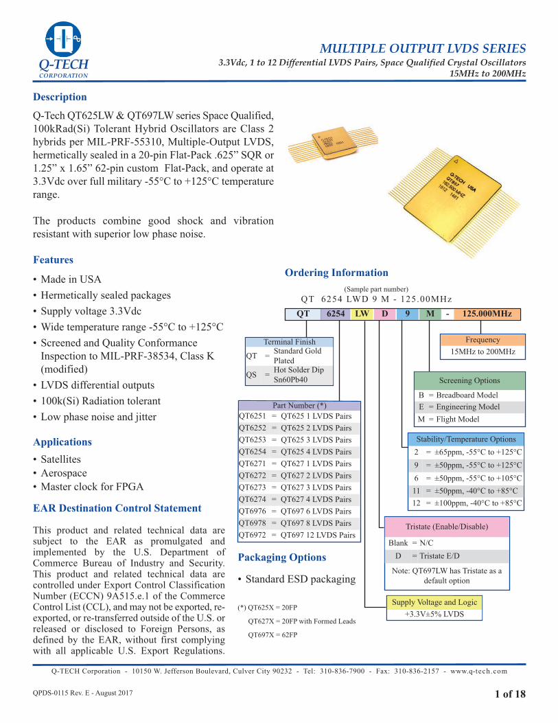
Q-Tech QT625LW & QT697LW series Space Qualified,100kRad(Si) Tolerant Hybrid Oscillators are Class 2hybrids per MIL-PRF-55310, Multiple-Output LVDS,hermetically sealed in a 20-pin Flat-Pack .625” SQR or1.25” x 1.65” 62-pin custom Flat-Pack, and operate at3.3Vdc over full military -55°C to +125°C temperaturerange.
The products combine good shock and vibrationresistant with superior low phase noise.
Features
• Made in USA• Hermetically sealed packages• Supply voltage 3.3Vdc • Wide temperature range -55°C to +125°C• Screened and Quality Conformance
Inspection to MIL-PRF-38534, Class K(modified)
• LVDS differential outputs • 100k(Si) Radiation tolerant• Low phase noise and jitter
Applications• Satellites• Aerospace• Master clock for FPGA
Ordering Information
Supply Voltage and Logic+3.3V±5% LVDS
Terminal Finish
QT = Standard GoldPlated
QS = Hot Solder DipSn60Pb40 Screening Options
B = Breadboard ModelE = Engineering Model M = Flight Model
QT 6254 LW D 9 M - 125.000MHz
(Sample part number)QT 6254 LWD 9 M - 125.00MHz
Packaging Options
• Standard ESD packaging
(*) QT625X = 20FP
QT627X = 20FP with Formed Leads
QT697X = 62FP
Stability/Temperature Options 2 = ±65ppm, -55°C to +125°C 9 = ±50ppm, -55°C to +125°C 6 = ±50ppm, -55°C to +105°C 11 = ±50ppm, -40°C to +85°C12 = ±100ppm, -40°C to +85°C
Frequency15MHz to 200MHz
Part Number (*)QT6251 = QT625 1 LVDS PairsQT6252 = QT625 2 LVDS PairsQT6253 = QT625 3 LVDS PairsQT6254 = QT625 4 LVDS PairsQT6271 = QT627 1 LVDS PairsQT6272 = QT627 2 LVDS PairsQT6273 = QT627 3 LVDS PairsQT6274 = QT627 4 LVDS PairsQT6976 = QT697 6 LVDS PairsQT6978 = QT697 8 LVDS PairsQT6972 = QT697 12 LVDS Pairs
Tristate (Enable/Disable)
Blank = N/CD = Tristate E/D
Note: QT697LW has Tristate as a default option
EAR Destination Control Statement
This product and related technical data aresubject to the EAR as promulgated andimplemented by the U.S. Department ofCommerce Bureau of Industry and Security.This product and related technical data arecontrolled under Export Control ClassificationNumber (ECCN) 9A515.e.1 of the CommerceControl List (CCL), and may not be exported, re-exported, or re-transferred outside of the U.S. orreleased or disclosed to Foreign Persons, asdefined by the EAR, without first complyingwith all applicable U.S. Export Regulations.

Q-TECH Corporation - 10150 W. Jefferson Boulevard, Culver City 90232 - Tel: 310-836-7900 - Fax: 310-836-2157 - www.q-tech.com
MULTIPLE OUTPUT LVDS SERIES3.3Vdc, 1 to 12 Differential LVDS Pairs, Space Qualified Crystal Oscillators
15MHz to 200MHzQ-TECHCORPORATION
QPDS-0115 Rev. E - August 2017 2 of 18
1 PURPOSE1.1 The purpose of this Specification Control Drawing (SCD) is to describe the design, construction, performance
and specific quality and reliability requirements for hermetically sealed 20-pin or 62-pin flat packs, Space Level, Hybrid Crystal Oscillators intended for use in high-reliability spacecraft applications.
2 SCOPE2.1 This specification establishes the minimum detail requirements for QT625LW, QT627LW, and QT697LW
intended for use in conjunction with the applicable documents.
3 PART PROTECTION AND SAFETY3.1 These items are susceptible to breakdown damage resulting from electrostatic discharge. Every precaution
shall be taken while handling, installing, and testing the parts to prevent static charge. Care should be exercised to not apply more than rated voltage or current to any terminal/pad during testing.
4 PART NUMBER4.1 The Q-Tech Part Number shall be as specified in Ordering Information.
5 APPLICABLE DOCUMENTATION & REFERENCES5.1 The following documents form a part of this drawing to the extent specified or modified herein.5.2 Military5.2.1 MIL-PRF-55310, Oscillator, Crystal Controlled, General Specification for5.2.2 MIL-PRF-19500, Semiconductor Devices, General Specification for5.2.3 MIL-PRF-38534, Microcircuit Manufacturing, General Specification for5.2.4 MIL-PRF-38535, Integrated Circuits, (Microcircuits) Manufacturing, General Specification for5.3 Standards5.3.1 MIL-STD-202, Test Methods for Electronic and Electrical Component Parts5.3.2 MIL-STD-750, Test Methods for Semiconductor Devices5.3.3 MIL-STD-883, Test Methods and Procedures for Microelectronics5.3.4 MIL-STD-1686, Electrostatic Discharge Control Program for Protection of Electrical and Electronic Parts,
Assemblies and Equipment5.3.5 MIL-STD-1285, Marking of Electrical and Electronic Parts5.3.6 MIL-STD-1580, Destructive Physical Analysis for EEE parts5.4 American Society for Testing And Materials5.4.1 ASTM E 595, Standard Test Method for Total Mass Loss and Collected Volatile Condensable materials from
Outgassing in a vacuum Environment5.5 Other Documents5.5.1 NASA Reference Publication 1124, Outgassing Data for Selecting Spacecraft Materials5.6 Order of Precedence
In the event of conflict between this document and the references cited herein or other requirements, the requirements of this drawing shall take precedence.
5.6.1 Customer Purchase Order Special RequirementsAdditional special requirements shall be specified in the applicable customer purchase order when additional requirements or modifications are needed for compliance to special programs or product line compliance. Unique identification of the items produced may be required.
6 REQUIREMENTS6.1 General Requirements
The parts shall comply with the requirements of MIL-PRF-38534, Class K and MIL-PRF-55310, Level S except as modified or supplemented herein.
Q-TECH Corporation - 10150 W. Jefferson Boulevard, Culver City 90232 - Tel: 310-836-7900 - Fax: 310-836-2157 - www.q-tech.com
MULTIPLE OUTPUT LVDS SERIES3.3Vdc, 1 to 12 Differential LVDS Pairs, Space Qualified Crystal Oscillators
15MHz to 200MHzQ-TECHCORPORATION
QPDS-0115 Rev. E - August 2017 3 of 18
6.2 Approved Source of SupplyHybrid crystal oscillators shall be supplied from the manufacturer specified in “Source of Supply” below.
6.3 Design and Construction6.3.1 Outline Dimensions and Terminal Connections
The outline dimensions and terminal connections shall be as shown in Figures 1 to 3 herein.6.3.2 Package Body and Lead Finish
The package body and lead finish shall be gold in accordance with MIL-PRF-38534. Hot Solder dip can be added as an option.
6.3.3 Circuit DesignThe circuit design analysis shall be performed to establish the electrical stresses for each element under the crystal oscillator nominal and maximum rated operating condition. The circuit design shall make allowances for worst-case variation, to compensate for manufacturing variations and End-Of- Life parameter limits in the following as a minimum, but not limited to: input and output voltages; input and output currents; power dissipation; propagation delay, frequency stability over temperature: frequency/voltage stability and operating junction temperature.
6.3.4 Quartz CrystalThe quartz crystal utilized in the design shall be Swept, grade 2.2 million or better, physically mounted on a three-point minimum.
6.3.5 Crystal MountingThe crystal element shall be three-point minimum mounted in such a manner as to assure adequate crystal performance when the oscillator is subjected to the environmental conditions specified herein.
6.3.6 Active DevicesThe microcircuit used in this part shall use LVDS technology and shall be from a wafer proven to be radiation tolerant to 100kRad(Si) total ionizing dose.
6.3.7 Element EvaluationAll piece parts shall be derived from lots that meet the element evaluation requirements of MIL-PRF- 38534, Class K.
6.3.8 Package ElementsSalt Spray Salt spray testing not required.
6.3.9 Electrical and Thermal DeratingThe derating analysis shall be performed using the maximum operating temperature specified in Table I.
6.3.10 Prohibited Finishes6.3.10.1 Metals
All metals (internal and external) shall be such that they will not promote the growth of whiskers, dentrites, intermetallic formation or Kirkendall voids, corrosion, and shall not sublime in the intended application conditions. Mercury, Zinc, Cadmium and Selenium are prohibited. Alloy and brazing materials containing Cadmium or Zinc shall not be used without over plating. Pure tin (greater than 97%) is prohibited. Tin shall bealloyed with a minimum of 3% lead (Pb) by weight.
6.3.10.2 Metal FinishesMetal finishes (internal and external) shall be such that they will not promote the growth of whiskers, dentrites, intermetallic formation or Kirkendall voids, corrosion, and shall not sublime in the intended application conditions. Pure tin (greater than 97%) is prohibited. Tin shall be alloyed with a minimum of 3% lead (Pb) by weight.
6.4 Performance Requirements6.4.1 Materials
Materials used in the device shall be in accordance with MIL-PRF-38534 and MIL-PRF-55310. The die interconnect materials, such as wires, shall be in accordance with MIL-PRF-38534, Class K.
6.4.2 Bimetallic Wire BondsBimetallic wire bonds at the die are used. However, the following process steps are implemented:
Q-TECH Corporation - 10150 W. Jefferson Boulevard, Culver City 90232 - Tel: 310-836-7900 - Fax: 310-836-2157 - www.q-tech.com
MULTIPLE OUTPUT LVDS SERIES3.3Vdc, 1 to 12 Differential LVDS Pairs, Space Qualified Crystal Oscillators
15MHz to 200MHzQ-TECHCORPORATION
QPDS-0115 Rev. E - August 2017 4 of 18
a) 100% Non-Destructive Bond Pull.b) Machine set-up, bond verification and in-process controls.
6.4.3 OutgassingAll nonmetallic and organic materials used shall meet outgassing requirements of ASTM E 595.
6.4.4 ReworkRework and rework qualification shall be in accordance with MIL-PRF-38534, Class K.
6.4.5 WeightThe weight of the device shall be less than 5 grams for QT625/627LW or less than 25 grams for QT697LW.
6.4.6 ESDS ClassificationThe Q-Tech ESDS classification for this part is Class 1C
6.4.7 MarkingThe marking shall be in accordance with Figure 1 to 3 herein.
6.4.8 SerializationEach unit shall have a unique serial number and be traceable to the specific date code, inspection lot and waferlot as required in MIL-PRF-38534, Class K.
6.4.9 Maximum RatingsThe maximum ratings shall be as specified in Table I herein.
6.4.10 Electrical Performance Characteristics and LimitsThe electrical performance requirements and limits shall be in accordance with Table III herein.
6.4.11 Maximum Allowable Leak RateThe maximum allowable leakage rate shall be as specified by MIL-STD-883, method 1014 based on the internal free cavity volume. The hermetic seal (fine and gross leak) tests shall be in accordance with MIL-STD-883, Method 1014.
6.4.12 Total Dose Radiation LimitsHybrid crystal oscillators shall be capable of meeting the performance requirements after being exposed to 100kRad(Si) total dose radiation levels.
6.4.13 Non-Flight OscillatorsFollowing general requirements for non-flight hardware shall apply as minimums:
6.4.13.1 Breadboard/Prototype (B) OscillatorsThe requirements for breadboard/prototype oscillators shall be as follows:a) Breadboard oscillators need only meet the form, fit and function of the flight units.b) Breadboard oscillators shall be suitable identified.
6.4.13.2 Engineering Model (E) OscillatorsThe requiremetns for engineering model oscillators shall be as follows:a) Design and manufacturing processes shall be identical to flight units.b) Finished units shall be functional over the operating temperature range.c) Screening test and/or Quality Conformance Inspection is not required.d) Engineering model oscillators shall be suitably identified.
7 QUALITY ASSURANCE PROVISIONS7.1 Responsiblility for Inspection
Unless otherwise specified in the contract or purchase order, the supplier shall be responsible for the performance of all inspection requirements as specified. Except as otherwise specified in the contract or purchase order, the supplier may use their own or any other facilities suitable for the performance of the inspection requirements specified herein, unless disapproved by Customer. Customer reserves the right to

Q-TECH Corporation - 10150 W. Jefferson Boulevard, Culver City 90232 - Tel: 310-836-7900 - Fax: 310-836-2157 - www.q-tech.com
MULTIPLE OUTPUT LVDS SERIES3.3Vdc, 1 to 12 Differential LVDS Pairs, Space Qualified Crystal Oscillators
15MHz to 200MHzQ-TECHCORPORATION
QPDS-0115 Rev. E - August 2017 5 of 18
perform any of the inspections set forth in the specification where such inspections are deemed necessary to assure supplies and services conform to prescribed requirements, and to return any product failing to meet the specified requirements.
7.2 ScreeningHybrid crystal oscillators shall have been subjected to and successfully passed all the screening tests as specified in Table IV herein in order to be acceptable for delivery. All variables data shall be read and recorded. Devices which fail any test criteria in the screening sequence shall be removed from the lot at the time of observation or immediately at the conclusion of the test in which the failure was observed. Once rejected and verified as a device failure, rework and subsequent rescreening in accordance with the rework provisions may be performed. Devices which fail during screening may be used for Group B inspection, provided that they have completed screening through completion of the burn-in testing.
7.2.1 Nondestructive Bond PullExcept for the wires connecting the crystal to the circuit (if available), 100 percent nondestructive bond pull, shall be performed on each hybrid crystal oscillator in accordance with MIL-STD-883, method 2023. The totalnumber of failed wires and the total number of devices failed shall be recorded. The lot shall have a percent defective allowable (PDA) of 2 percent or less based on the total number of wires pulled in the production lot.
7.2.2 Internal Visual InspectionInternal visual inspection shall be in accordance with the condition K (class S) requirements of MIL-STD-883,methods 2017 and 2032. During the time interval between final internal visual inspection and preparation for sealing, hybrid crystal oscillators shall be stored in a dry, controlled environment as defined in MIL-STD-883,method 2017 or in a vacuum bake oven. The following details shall apply:a) The final internal visual inspection shall occur after crystal resonator installation and prior to cover seal.
Hybrid crystal oscillator inspection and preparation for sealing shall be in a class 100 environment as defined in Federal Standard 209. Hybrid crystal oscillators shall be in a covered container when transferred from one controlled environment to another.
7.2.3 Stabilization BakeStabilization bake shall be performed prior to package seal. Stabilization bake shall be performed in a vacuum environment.
7.2.4 Temperature CyclingUnless otherwise specified, temperature cycling shall be in accordance with Table IV herein.
7.2.5 Constant AccelerationConstant acceleration shall be performed in the Y1 orientation.
7.2.6 Particle Impact Noise Detection (PIND) TestPIND testing shall be performed in accordance with MIL-STD-883, method 2020, condition B. The PIND testshall be performed using five independent passes and all failures found at the end of each pass are rejected. The survivors of the last pass are acceptable. The cumulative number of defective devices shall not exceed 25 percent.
7.2.7 Pre Burn-In Electrical Characteristics TestUnless otherwise specified, pre burn-in electrical testing shall consist of the tests listed in Table IX. Electrical performance limits shall be in accordance with Table III.
7.2.8 Burn-InThe burn-in period shall be 320 hours minimum. The 320 hour burn-in period shall be divided into two successive 160 hour minimum burn-in periods. Electrical testing shall be performed after the first burn-in to select acceptable devices for the second burn-in.
7.2.9 Interim Electrical TestingUnless otherwise specified, interim electrical testing shall consist of the tests listed in Table IX. Electrical performance limits shall be in accordance with Table III.
7.2.10 Final Electrical TestingUnless otherwise specified, final electrical testing shall consist of the tests listed in Table IX. Electrical performance limits shall be in accordance with Table III.

Q-TECH Corporation - 10150 W. Jefferson Boulevard, Culver City 90232 - Tel: 310-836-7900 - Fax: 310-836-2157 - www.q-tech.com
MULTIPLE OUTPUT LVDS SERIES3.3Vdc, 1 to 12 Differential LVDS Pairs, Space Qualified Crystal Oscillators
15MHz to 200MHzQ-TECHCORPORATION
QPDS-0115 Rev. E - August 2017 6 of 18
7.2.10.1 Delta Limits ReviewUnless otherwise specified, delta limits shall be in accordance with Table II herein.
7.2.10.2 Percent Defective Allowable (PDA)The percent defective allowable shall be 2 percent or one device, whichever is greater. PDA accountability shall be based on failures occurring during the second half of burn-in only. PDA shall be applicable to the +25 ºC of current test only.
7.2.11 Seal TestThe seal test may be performed in any sequence between the final electrical test and the external visual, but it shall be performed after all shearing and forming operations on the terminals. All hybrid crystal oscillators having any physical processing steps (e.g. solder dipping to the glass seal, etc.) performed following seal or external visual shall be retested for hermeticity and visual defects.
7.2.12 Radiographic InspectionRadiographic inspection shall be performed in accordance with MIL-STD-883, method 2012. Views X, Y and Z axis.
7.2.13 Frequency AgingThe energized oscillator(s) shall be maintained at a temperature of 70 ± 3 °C for a continuous period of 30 days. Unless otherwise specified, the frequency of the oscillator shall be measured in accordance with MIL-PRF-55310. The measuring instrument's accuracy shall be commensurable with the required accuracy of the oscillator. The same measuring instruments shall be used throughout the aging test. If any condition develops that will change the temperature of the oscillator from the aging temperature for a time interval of more than one hour, no measurement shall be made until 24 hours after the temperature restoration and the specified test period shall be lengthened by the length of time that the temperature failed. Tests may be terminated after 15 days if the drifts do not exceed one-half of the specified Aging rate.
7.2.14 External VisualThe final external visual screen shall be conducted in accordance with MIL-STD-883, method 2009 after all other 100 percent screens have been performed to determine that no damage to or contamination of the package exterior has occurred.
7.3 Quality Conformance Inspection (QCI)Quality conformance inspection shall be as specified herein. All records shall be traceable to the lot number and unit serial number.
7.3.1 Oscillator Group A InspectionGroup A testing shall be in accordance with Table V. Group A inspection shall be performed on units that have passed the screening tests. All electrical perfomance tests of this specification shall be performed during Group A with the exception of any tests performed as part of final electrical testing during 100 percent screening.
7.3.2 Oscillator Group B InspectionGroup B inspection shall be in accordance with Table VI. The screening test rejects may be used for this test.
7.3.3 Oscillator Group C InspectionGroup C inspection shall be in accordance with Table VII.
7.3.4 Oscillator Group D InspectionGroup D inspection shall be performed per Table VIII. The generic package evaluation data may be submitted to Customer for review in lieu of performing this test.
7.3.4.1 Group D SamplesSealed empty packages that have been subjected to the handling and stress conditions may be used for GroupD testing.
7.4 Destructive Physical Analysis (DPA)A DPA may be performed on each lot of devices in accordance with MIL-STD-883, Method 5009. The DPA shall be performed by the Customer.

Q-TECH Corporation - 10150 W. Jefferson Boulevard, Culver City 90232 - Tel: 310-836-7900 - Fax: 310-836-2157 - www.q-tech.com
MULTIPLE OUTPUT LVDS SERIES3.3Vdc, 1 to 12 Differential LVDS Pairs, Space Qualified Crystal Oscillators
15MHz to 200MHzQ-TECHCORPORATION
QPDS-0115 Rev. E - August 2017 7 of 18
7.5 WorkmanshipDevices shall be manufactured, processed, and tested in a careful and workmanlike manner in accordance withgood engineering practice, with the requirements of this specification, and with the production practices, workmanship instructions and inspections and test procedures prepared by the manufacturer in fulfillment of the product assurance program.
7.6 DATA7.6.1 Design and Part Configuration Documentation
The manufacturer shall establish baseline documentation sufficient to completely define and control the configuration of devices supplied to this specification. The documentation shall form the basis for defining thedevice qualified to this specification and all devices supplied on subsequent procurement shall be the same as those that qualified. No changes in construction, technology, or manufacturing processing shall occur without Customer approval.
7.6.2 Design DocumentationWhen required by the purchase order, design, topography, schematic circuit, process and flow charts for all assembly/inspection and test operation for devices to be supplied under this specification on the initial procurement shall be established and shall be available in-plant for review by the procuring activity upon request. This design documentation shall be sufficient to depict the physical and electrical construction of the devices supplied under the specification and shall be traceable to the specific parts, drawings or part type numbers to which it applies, and to the production lot(s) and inspection lot codes under which devices are manufactured and tested so that revisions can be identified.
7.6.2.1 Technical Data PackageWhen required by purchase order, the following design documentation and information is deliverable 30 days prior to the start of production. The Technical Data Package shall consist of the following:a) Assembly drawing(s).b) All electrical schematics and drawings not considered proprietary.c) The assembly and screening travelers to be used on-line to manufacture the devices supplied to this
specification.d) Parts and materials list.
7.6.3 Design Documentation ApprovalAfter the design documentation is approved by Customer, any changes or revisions to these documents must be submitted for review and approval to Customer prior to processing subsequent lots, or at the time of placement of subsequent purchase order.
7.7 Test ReportA test report shall be supplied with each shipment of oscillators and shall include the following information, as a minimum:a) A Certificate of Conformance to all specifications and purchase order requirements. As a minimum, the
Certificate of Conformance shall include the following information:1) Purchase order number.2) Applicable part number.3) Manufacturers lot number.4) Lot date code.
b) Parts and materials traceability information.c) Certificate of crystal sweeping.d) Manufacturing lot traveler.e) Screening attributes and variables data as applicable.f) Quality conformance inspection attributes and variables data as applicable.g) Radiographic inspection negatives.
Q-TECH Corporation - 10150 W. Jefferson Boulevard, Culver City 90232 - Tel: 310-836-7900 - Fax: 310-836-2157 - www.q-tech.com
MULTIPLE OUTPUT LVDS SERIES3.3Vdc, 1 to 12 Differential LVDS Pairs, Space Qualified Crystal Oscillators
15MHz to 200MHzQ-TECHCORPORATION
QPDS-0115 Rev. E - August 2017 8 of 18
7.8 Problem ReportingThe manufacturer shall notify the Customer technical representative, within 24 hours, of the occurrence of the following:a) Any failures detected during quality conformance inspection.b) Delays resulting from test equipment breakdown, test error, or testing related problems that adversely
affect the schedule.7.9 Customer Source Inspection
Provisions for periodic in-process source inspection by Customer shall be included in the supplier's manufacturing plan. The supplier shall provide Customer 72 hours minimum notice when the deliverable devices are ready for an in-process source inspection. The inspection points shall, as a minimum, be:a) Pre cap visual inspection.b) Prior to shipment inspection.
7.10 Retention of RecordsAll records pertaining to the design, processes, incoming receiving, in-process inspections, screening and quality conformance inspection, product lot identification, product traceability, failure reports and analyses etc., shall be retained by the vendor for a period of 10 years from the date of product shipment.
8 PREPARATION FOR DELIVERY8.1 Packaging
The requirements for packaging shall be in accordance with MIL-PRF-55310.8.2 Electrostatic Discharge Sensitivity
The devices supplied to this drawing shall be considered to be electrostatic discharge sensitive and require further protection and shall use one of the packaging requirements in accordance with MIL-PRF-38534.
9 NOTES9.1 Ordering Data
The contract or purchase order should specify the following:a) Customer part number.b) Quality Conformance Inspection requirements.c) Requirements for special technical documentation Data Package.d) Test data requirements.e) Special packaging.f) Requirement for source inspection and notification.
9.2 HandlingThe devices used must be handled with certain precautions to avoid damage due to electrostatic discharge.
9.3 Certificate of ConformanceCertificate of conformance to this specification, signed by an authorized representative of the manufacturer,shall accompany each shipment.
9.4 Approved Sources of Supply9.4.1 Approved Manufacturer
Q-Tech Corporation10150 West Jefferson BoulevardCulver City, CA 90232-3510 USA
Q-TECH Corporation - 10150 W. Jefferson Boulevard, Culver City 90232 - Tel: 310-836-7900 - Fax: 310-836-2157 - www.q-tech.com
MULTIPLE OUTPUT LVDS SERIES3.3Vdc, 1 to 12 Differential LVDS Pairs, Space Qualified Crystal Oscillators
15MHz to 200MHzQ-TECHCORPORATION
QPDS-0115 Rev. E - August 2017 9 of 18
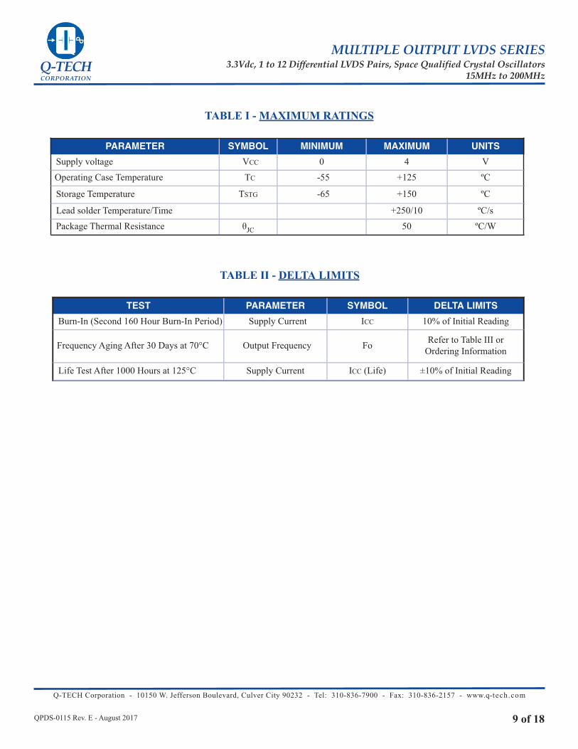
PARAMETER SYMBOL MINIMUM MAXIMUM UNITSSupply voltage VCC 0 4 V
Operating Case Temperature TC -55 +125 ºC
Storage Temperature TSTG -65 +150 ºC
Lead solder Temperature/Time +250/10 ºC/s
Package Thermal Resistance θJC 50 ºC/W
TABLE I - MAxIMuM RATINgS
TEST PARAMETER SYMBOL DELTA LIMITSBurn-In (Second 160 Hour Burn-In Period) Supply Current ICC 10% of Initial Reading
Frequency Aging After 30 Days at 70°C Output Frequency Fo Refer to Table III or Ordering Information
Life Test After 1000 Hours at 125°C Supply Current ICC (Life) ±10% of Initial Reading
TABLE II - DELTA LIMITS

Q-TECH Corporation - 10150 W. Jefferson Boulevard, Culver City 90232 - Tel: 310-836-7900 - Fax: 310-836-2157 - www.q-tech.com
MULTIPLE OUTPUT LVDS SERIES3.3Vdc, 1 to 12 Differential LVDS Pairs, Space Qualified Crystal Oscillators
15MHz to 200MHzQ-TECHCORPORATION
QPDS-0115 Rev. E - August 2017 10 of 18
ELECTRICAL PARAMETERS
TEST CONDITIONS(NOTE 2 AND 3)
LIMITSNOTES
MIN. TYP MAX UNITFrequency/Temperature Stability See Temp Code See code ppm Note 1, 4Supply Voltage 3.135 3.3 3.465 Vdc
Input Current Icc @3.465V - - 80120 mA QT625LW/QT627LW
QT697LWLoad 90 100 110 Note 6Output Voltage – Logic “0” 0.9 - - Vdc Note 5Output Voltage – Logic “1” - - 1.6 Vdc Note 5Differential voltage VOD 250 - 460 mVOutput Waveform SQUARE
Rise Time and Fall Time15MHz – 100MHz 1
ns Note 7>100MHz – 200MHz 0.6
Duty Cycle 45 55 %
Frequency Aging (After 30 Days) 70°C ± 3°C±1.5±2±3
ppm15MHz to <150MHz
150MHz to <162.5 MHz162.4MHz to 200MHz
Frequency Aging (After 1 Year) 70°C ± 3°C ±10 ppmFrequency Aging (After 15 Years) 70°C ± 3°C ±45 ppmStart Up Time 10 msec
Single side band phase noiseFrequency offset
100kHz 1MHz
-145-150 dBc/Hz
Integrated phase jitter (RMS) Integrated over12kHz to 20MHz - - 1 ps
Frequency/voltage stability RL=100ohms - - ±2 ppm
Frequency/load stability 3.3Vdc ±10% of Load - - ±1 ppm
Skew between outputs - - 0.4 ns Note 8
NOTES1. The limit for Frequency temperature stability is referenced to the nominal output frequency F0.2. Unless otherwise specified, the limits are over the full operating temperature range, and under specified load conditions
and nominal Supply Voltage.3. Unless otherwise specified, all measurements are in accordance with MIL-PRF-55310.4. Reference to nominal frequency up to 30 days after shipment (does not include aging).5. Voltage values are with respect to network ground terminal.6. Load is 100ohms typical.7. Measured between 20% and 80% and 80% to 20%.8. Guaranteed by design, not tested.
TABLE III - ELECTRICAL PERFORMANCE CHARACTERISTICSSupply Voltage (Vdd) = +3.3V±5%, unless otherwise specified

Q-TECH Corporation - 10150 W. Jefferson Boulevard, Culver City 90232 - Tel: 310-836-7900 - Fax: 310-836-2157 - www.q-tech.com
MULTIPLE OUTPUT LVDS SERIES3.3Vdc, 1 to 12 Differential LVDS Pairs, Space Qualified Crystal Oscillators
15MHz to 200MHzQ-TECHCORPORATION
QPDS-0115 Rev. E - August 2017 11 of 18
TEST DESCRIPTION STANDARD METHOD CONDITION COMMENTSNondestructive Bond Pull 883 2023 2.4-Gram PullInternal Visual 883 2017 K Class SStabilization Bake 883 1008 C, 48 Hours at 150°CTemperature Cycling 883 1010 C , 10 CyclesConstant Acceleration 883 2001 A, Y1 Direction Only
Particle Impact Noise Detection (PIND) 883 2020 B 5 PassesNote 1
Pre Burn-In Electrical Test Note 2Burn-In # 1 883 1015 125°C for 160 hours Note 3Interim Electrical Test Note 2Burn-In # 2 883 1015 125°C for 160 hours Note 3Final Electrical Test Note 2Percent Defective Allowance (PDA) 2% or 1 unit, whichever is greater Note 4Delta Limit Refer to Table II hereinSeal; Fine Leak 883 1014 B1Seal; Gross Leak 883 1014 B2Radiographic Inspection 883 2012Frequency Aging MIL-PRF-55310 - 70 ± 3°C for 30 days Note 5External Visual 883 2009
NOTES1. PIND testing shall be performed using five (5) independent passes and all failures found at the end of each pass are
rejected. The survivors of the last pass are acceptable.2. Electrical performance characteristic and requirements shall be in accordance with Table III and Table IX herein.3. Burn-in shall be under the specified load and nominal voltage conditions.4. Percent defective allowable (PDA) accountability shall be based on failures occurring during the second half of burn-in
only. PDA shall be applicable to the +25°C of current test only.5. Frequency Aging tests may be terminated after 15 days if the drifts do not exceed one-half of the delta limits specified.
TABLE IV - SCREENING TESTS

Q-TECH Corporation - 10150 W. Jefferson Boulevard, Culver City 90232 - Tel: 310-836-7900 - Fax: 310-836-2157 - www.q-tech.com
MULTIPLE OUTPUT LVDS SERIES3.3Vdc, 1 to 12 Differential LVDS Pairs, Space Qualified Crystal Oscillators
15MHz to 200MHzQ-TECHCORPORATION
QPDS-0115 Rev. E - August 2017 12 of 18
TABLE V - GROUP A INSPECTION
SUBGROUP TEST DESCRIPTION MIL-STD-833 Quantity (Accept No.)METHOD CONDITION
1 Physical Dimension 2016 2 (0)2 Resistance To Solvents 2015 3 (0)3 Internal Visual And Mechanical 2014 1 (0)4 Bond Strength (Note 2) 2011 C or D 2 (0)5 Die Shear Strength (Note 3) 2019 2 (0)6 Solderability (Note 4) 2003 Solder Temperature: +245 ±5°C 1 (0)
TABLE VI - GROUP B INSPECTION(Note 1)
NOTES1. Non catastrophic screening test rejects may be used for group B.2. Bond Strength Test shall be performed in accordance requirements of MIL-PRF-38534. This test is may be per
formed in-process any time prior to cover seal.3. Die shear test samples shall not be the same units as subjected to bond pull. Die shear specimens shall not be ex
posed to the 300°C preconditioning used for the Bond Strength test.4. Solder temperature shall be 245 +5°C.
TEST DESCRIPTION CONDITIONSupply Current 25°C and Temperature ExtremesInitial Accuracy 25°C
Frequency-Temperature StabilityOver specified operating temperature range, measures output frequency
at minimum eleven equispaced points of the temperature. Test points shall include reading at room temperature.
Frequency-Voltage Tolerance
25°C and Temperature Extremes
Output VoltagesDuty Cycle (Output Waveform Symmetry)Output Rise And Fall TimesStart-Up TimeJitter Phase NoiseDifferential Voltage VODFrequency/Load Stability
NOTES1. All electrical performance shall be performed during Group A with the exception of any tests performed as part of
the final electrical testing during 100 percent screening.2. Electrical performance characteristics and requirements shall be in accordance with Table III and Table IX herein.

Q-TECH Corporation - 10150 W. Jefferson Boulevard, Culver City 90232 - Tel: 310-836-7900 - Fax: 310-836-2157 - www.q-tech.com
MULTIPLE OUTPUT LVDS SERIES3.3Vdc, 1 to 12 Differential LVDS Pairs, Space Qualified Crystal Oscillators
15MHz to 200MHzQ-TECHCORPORATION
QPDS-0115 Rev. E - August 2017 13 of 18
TABLE VII - GROUP C INSPECTION(Note 1)
SUBGROUP TEST DESCRIPTION MIL-STD-833 Quantity (Accept No.)METHOD CONDITION
1
Thermal Shock 1011 C 5 (0)Stabilization Bake 1008 1 Hour at 150°C 5 (0)
Lead Integrity 2004 B2 (Lead Fatigue) 1 (0)
Seal; Fine Leak and Gross Leak 1014 B1 and B2 5 (0)
TABLE VIII - GROUP D INSPECTION(Note 1)
NOTES1. This testing may be accomplished during package evaluation at incoming inspection and need not be repeated. Testing may also be perfomed on a sealed empty package.
SUBGROUP TEST DESCRIPTION MIL-STD-833 Quantity (Accept No.)METHOD CONDITION
1
External visual 2009
5 (0)
Temperature cycling 1010 C, 20 cyclesConstant acceleration 2001 A, Y1 Direction Only
Seal (fine & gross leak) 1014 B1 & B2Radiographic inspection 2012
Visual exmination 2009End point electricals
2
End point electricals
5 (0)Steady state life test 1005 125°C,1,000 hours min.
End point electricals3 Internal wator vapor content 1018 3 (0) or 5 (1)
NOTES1. It is recommended to use 10 specimens for Group C Inspection - 5 units for Subgroups 1 and 3 and 5 units for
Subgroup 2. 5 units may be used for Group C Inspection but the Customer procures this quantity at their own risk. Usage of specimens that have completed Subgroups 1 and 2 Testing for Subgroup 3 Testing is not recommended. This limited acquisition shall only be used if this risk is acceptable to the Customer, and the Customer assumes responsibility for Subgroup 3 failures if only five units are procured for Group C Inspection.
2. Subgroup 3 Testing shall only use specimens that have completed Subgroup 1 Testing.3. End point electricals shall be as specified in accordance with Table III and Table IX herein.
Q-TECH Corporation - 10150 W. Jefferson Boulevard, Culver City 90232 - Tel: 310-836-7900 - Fax: 310-836-2157 - www.q-tech.com
MULTIPLE OUTPUT LVDS SERIES3.3Vdc, 1 to 12 Differential LVDS Pairs, Space Qualified Crystal Oscillators
15MHz to 200MHzQ-TECHCORPORATION
QPDS-0115 Rev. E - August 2017 14 of 18
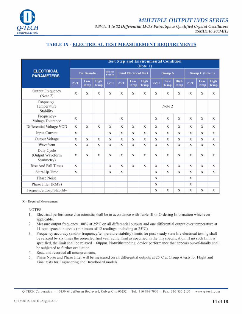
ELECTRICAL PARAMETERS
Test Step and Environmental Condition(Note 1)
Pre Burn-In InterimBurn-In Final Electrical Test Group A Group C (Note 3)
25°C LowTemp
HighTemp 25°C 25°C Low
TempHighTemp 25°C Low
TempHighTemp 25°C Low
TempHighTemp
Output Frequency(Note 2) X X X X X X X X X X X X X
Frequency- Temperature
StabilityNote 2
Frequency-Voltage Tolerance X X X X X X X X
Differential Voltage VOD X X X X X X X X X X X X X
Input Current X X X X X X X X X X X
Output Voltage X X X X X X X X X X X X X
Waveform X X X X X X X X X X X X X
Duty Cycle (Output Waveform
Symmetry)X X X X X X X X X X X X X
Rise And Fall Times X X X X X X X X X X X
Start-Up Time X X X X X X X X X
Phase Noise X X
Phase Jitter (RMS) X X
Frequency/Load Stability X X X X X X
NOTES1. Electrical performance characteristic shall be in accordance with Table III or Ordering Information whichever
applicable.2. Measure output frequency 100% at 25°C on all differential outputs and one differential output over temperature at 11 equi-spaced intervals (minimum of 12 readings, including at 25°C).3. Frequency accuracy (and/or frequency/temperature stability) limits for post steady state life electrical testing shall
be relaxed by six times the projected first year aging limit as specified in the this specification. If no such limit is specified, the limit shall be relaxed ± 60ppm. Notwithstanding, device performance that appears out-of-family shall be subjected to further evaluation.
4. Read and recorded all measurements.5. Phase Noise and Phase Jitter will be measured on all differential outputs at 25°C at Group A tests for Flight and Final tests for Engineering and Breadboard models.
TABLE IX - ELECTRICAL TEST MEASUREMENT REQUIREMENTS
X = Required Measurement
Q-TECH Corporation - 10150 W. Jefferson Boulevard, Culver City 90232 - Tel: 310-836-7900 - Fax: 310-836-2157 - www.q-tech.com
MULTIPLE OUTPUT LVDS SERIES3.3Vdc, 1 to 12 Differential LVDS Pairs, Space Qualified Crystal Oscillators
15MHz to 200MHzQ-TECHCORPORATION
QPDS-0115 Rev. E - August 2017 15 of 18
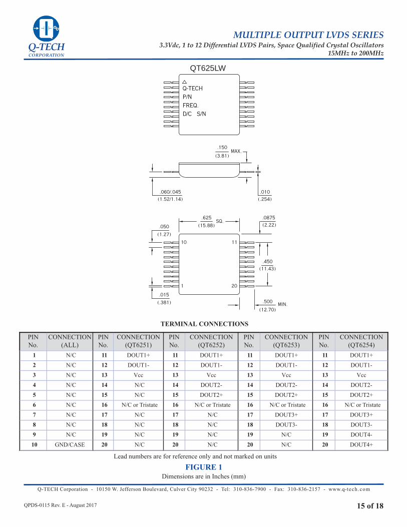
.015
(.381)
(1.27)
.050
.450
(11.43)
.625
(15.88)
(.254)
.010.060/.045
(1.52/1.14)
(3.81)
.150
FREQ.P/NQ-TECH
20
1110
1
MAX.
SQ.
D/C S/N
.500
(12.70) MIN.
.0875
(2.22)
FIguRE 1Dimensions are in Inches (mm)
QT625LW
PIN No.
CONNECTION(ALL)
PINNo.
CONNECTION(QT6251)
PINNo.
CONNECTION(QT6252)
PINNo.
CONNECTION(QT6253)
PINNo.
CONNECTION(QT6254)
1 N/C 11 DOUT1+ 11 DOUT1+ 11 DOUT1+ 11 DOUT1+
2 N/C 12 DOUT1- 12 DOUT1- 12 DOUT1- 12 DOUT1-
3 N/C 13 Vcc 13 Vcc 13 Vcc 13 Vcc
4 N/C 14 N/C 14 DOUT2- 14 DOUT2- 14 DOUT2-
5 N/C 15 N/C 15 DOUT2+ 15 DOUT2+ 15 DOUT2+
6 N/C 16 N/C or Tristate 16 N/C or Tristate 16 N/C or Tristate 16 N/C or Tristate
7 N/C 17 N/C 17 N/C 17 DOUT3+ 17 DOUT3+
8 N/C 18 N/C 18 N/C 18 DOUT3- 18 DOUT3-
9 N/C 19 N/C 19 N/C 19 N/C 19 DOUT4-
10 GND/CASE 20 N/C 20 N/C 20 N/C 20 DOUT4+
TERMINAL CONNECTIONS
Lead numbers are for reference only and not marked on units

Q-TECH Corporation - 10150 W. Jefferson Boulevard, Culver City 90232 - Tel: 310-836-7900 - Fax: 310-836-2157 - www.q-tech.com
MULTIPLE OUTPUT LVDS SERIES3.3Vdc, 1 to 12 Differential LVDS Pairs, Space Qualified Crystal Oscillators
15MHz to 200MHzQ-TECHCORPORATION
QPDS-0115 Rev. E - August 2017 16 of 18
FIguRE 2Dimensions are in Inches
PIN No.
CONNECTION(ALL)
PINNo.
CONNECTION(QT6271)
PINNo.
CONNECTION(QT6272)
PINNo.
CONNECTION(QT6273)
PINNo.
CONNECTION(QT6274)
1 N/C 11 DOUT1+ 11 DOUT1+ 11 DOUT1+ 11 DOUT1+
2 N/C 12 DOUT1- 12 DOUT1- 12 DOUT1- 12 DOUT1-
3 N/C 13 Vcc 13 Vcc 13 Vcc 13 Vcc
4 N/C 14 N/C 14 DOUT2- 14 DOUT2- 14 DOUT2-
5 N/C 15 N/C 15 DOUT2+ 15 DOUT2+ 15 DOUT2+
6 N/C 16 N/C or Tristate 16 N/C or Tristate 16 N/C or Tristate 16 N/C or Tristate
7 N/C 17 N/C 17 N/C 17 DOUT3+ 17 DOUT3+
8 N/C 18 N/C 18 N/C 18 DOUT3- 18 DOUT3-
9 N/C 19 N/C 19 N/C 19 N/C 19 DOUT4-
10 GND/CASE 20 N/C 20 N/C 20 N/C 20 DOUT4+
TERMINAL CONNECTIONS
Lead numbers are for reference only and not marked on units
.010 ± .002
.145 ± .003
2 X.450 ± .005
20
1110
1
Q-TECHP/NFREQ.D/C S/N
.058 ± .003
.060 ± .003
20 X .145 ± .00520 X .015 ± .003
18 X .048 ± .003
.625 ± .005 SQ.
.004 ± .001
.100 ± .020
QT627LW
Q-TECH Corporation - 10150 W. Jefferson Boulevard, Culver City 90232 - Tel: 310-836-7900 - Fax: 310-836-2157 - www.q-tech.com
MULTIPLE OUTPUT LVDS SERIES3.3Vdc, 1 to 12 Differential LVDS Pairs, Space Qualified Crystal Oscillators
15MHz to 200MHzQ-TECHCORPORATION
QPDS-0115 Rev. E - August 2017 17 of 18
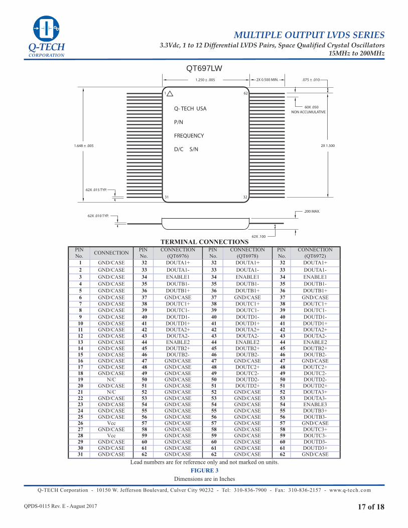
Q- TECH USA
P/N
FREQUENCY
D/C S/N
1.250 ± .005 2X 0.500 MIN. .075 ± .010
60X .050NON ACCUMULATIVE
2X 1.5001.648 ± .005
62X .015 TYP.
62X .010 TYP..200 MAX.
62X .100
1
31 32
62
PIN No. CONNECTION PIN
No.CONNECTION
(QT6976)PIN No.
CONNECTION(QT6978)
PIN No.
CONNECTION(QT6972)
1 GND/CASE 32 DOUTA1+ 32 DOUTA1+ 32 DOUTA1+2 GND/CASE 33 DOUTA1- 33 DOUTA1- 33 DOUTA1-3 GND/CASE 34 ENABLE1 34 ENABLE1 34 ENABLE14 GND/CASE 35 DOUTB1- 35 DOUTB1- 35 DOUTB1-5 GND/CASE 36 DOUTB1+ 36 DOUTB1+ 36 DOUTB1+6 GND/CASE 37 GND/CASE 37 GND/CASE 37 GND/CASE7 GND/CASE 38 DOUTC1+ 38 DOUTC1+ 38 DOUTC1+8 GND/CASE 39 DOUTC1- 39 DOUTC1- 39 DOUTC1-9 GND/CASE 40 DOUTD1- 40 DOUTD1- 40 DOUTD1-10 GND/CASE 41 DOUTD1+ 41 DOUTD1+ 41 DOUTD1+11 GND/CASE 42 DOUTA2+ 42 DOUTA2+ 42 DOUTA2+12 GND/CASE 43 DOUTA2- 43 DOUTA2- 43 DOUTA2-13 GND/CASE 44 ENABLE2 44 ENABLE2 44 ENABLE214 GND/CASE 45 DOUTB2+ 45 DOUTB2+ 45 DOUTB2+15 GND/CASE 46 DOUTB2- 46 DOUTB2- 46 DOUTB2-16 GND/CASE 47 GND/CASE 47 GND/CASE 47 GND/CASE17 GND/CASE 48 GND/CASE 48 DOUTC2+ 48 DOUTC2+18 GND/CASE 49 GND/CASE 49 DOUTC2- 49 DOUTC2-19 N/C 50 GND/CASE 50 DOUTD2- 50 DOUTD2-20 GND/CASE 51 GND/CASE 51 DOUTD2+ 51 DOUTD2+21 N/C 52 GND/CASE 52 GND/CASE 52 DOUTA3+22 GND/CASE 53 GND/CASE 53 GND/CASE 53 DOUTA3-23 GND/CASE 54 GND/CASE 54 GND/CASE 54 ENABLE324 GND/CASE 55 GND/CASE 55 GND/CASE 55 DOUTB3+25 GND/CASE 56 GND/CASE 56 GND/CASE 56 DOUTB3-26 Vcc 57 GND/CASE 57 GND/CASE 57 GND/CASE27 GND/CASE 58 GND/CASE 58 GND/CASE 58 DOUTC3+28 Vcc 59 GND/CASE 59 GND/CASE 59 DOUTC3-29 GND/CASE 60 GND/CASE 60 GND/CASE 60 DOUTD3-30 GND/CASE 61 GND/CASE 61 GND/CASE 61 DOUTD3+31 GND/CASE 62 GND/CASE 62 GND/CASE 62 GND/CASE
Lead numbers are for reference only and not marked on units.FIguRE 3
Dimensions are in Inches
TERMINAL CONNECTIONS
QT697LW

Q-TECH Corporation - 10150 W. Jefferson Boulevard, Culver City 90232 - Tel: 310-836-7900 - Fax: 310-836-2157 - www.q-tech.com
MULTIPLE OUTPUT LVDS SERIES3.3Vdc, 1 to 12 Differential LVDS Pairs, Space Qualified Crystal Oscillators
15MHz to 200MHzQ-TECHCORPORATION
QPDS-0115 Rev. E - August 2017 18 of 18
DCO REV REVISION SuMMARY PAgE DATE
6433 C Change max frequency from 162.5MHz to 200MHz All 2/14/17
6876 DAdd Stability/Temperature option code 12
1 5/25/2017Add EAR Destination Control Statement
7163 E
Add QT627 (formed leads) package with revisions to references of pack-age Figure Numbers. 1 - 4, 10, 16
8/28/2017Table III: Add QT627 to Icc notes columnAdd ±10% Load to Load StabilityAdd Note 8 to ‘Skew between outputs’
10