multipacting simulation study for 56 mhz quarter …public.bnl.gov/docs/cad/documents/multipacting...
TRANSCRIPT

BNL-81971-2009-IR
C-A/AP/#343 January 2009
Multipacting simulation study for 56 MHz Quarter Wave Resonator using 2D code
D. Naik, I. Ben-Zvi
Collider-Accelerator Department Brookhaven National Laboratory
Upton, NY 11973
Notice: This document has been authorized by employees of Brookhaven Science Associates, LLC under Contract No. DE-AC02-98CH10886 with the U.S. Department of Energy. The United States Government retains a non-exclusive, paid-up, irrevocable, world-wide license to publish or reproduce the published form of this document, or allow others to do so, for United States Government purposes.

Multipacting simulation study for 56 MHz Quarter Wave Resonator using 2D code
Damayanti Naik, Ilan Ben-Zvi
Abstract
A beam excited 56 MHz Radio Frequency (RF) Niobium Quarter Wave Resonator (QWR) has
been proposed to enhance RHIC beam luminosity and bunching. Being a RF cavity, multipacting
is expected; therefore an extensive study was carried out with the Multipac 2.1 2D simulation
code. The study revealed that multipacting occurs in various bands up to peak surface electric
field 50 kV/m and is concentrated mostly above the beam gap and on the outer conductor. To
suppress multipacting, a ripple structure was introduced to the outer conductor and the
phenomenon was successfully eliminated from the cavity.
1

1. Introduction: Multipacting, a highly probable phenomenon in all RF structures, is an electron
avalanche phenomenon caused by resonating electron multiplication due to secondary emission
[1, 2]. Starting from the walls or inside the cavity, the electrons gain energy from the RF field
and follow a repetitive path. As the electrons hit the cavity wall, and depending on the secondary
yield (δ) of the wall’s material, they accumulate in greater numbers thus creating an electron
cloud. The cloud absorbs much of the power pumped into the system and prevents the structure
from functioning at its full capacity. The impacts of the electrons on the cavity wall raise its
temperature, this fact is important for superconducting material as it may quench
superconductivity. Symmetry in RF structures also increases the probability of multipacting. The
56 MHz Quarter Wave Resonator (QWR) [3], (shown in Fig. 1) has a symmetrical structure,
made up of the superconducting material niobium, and thereby susceptible to sever multipacting
[2]. A brief simulation of this process in the cavity was therefore carried out with both 2D and
3D code. However, at first, simulation was carried out without coupler and dampers in the cavity
with Multipac 2.1 2D code [4] and the present article discusses the results and a method to
suppress multipacting in this cavity.
Fig. 1. The outline of the 56 MHz RF Quarter Wave Resonator in 2-Dimension without coupler and dampers.
2. Simulation code features: Linux based Multipac 2.1 2D code, works for axial symmetric RF
structure. Without coupler and dampers, the cavity has an axial symmetric geometry, hence the
Multipac 2.1 code can be employed in this problem. Based on the Finite Element Method field
solver, the code calculates the time harmonic electromagnetic field. Thereafter it locates
multipacting field levels, aided by data on the secondary yield of the cavity material (Fig. 2
shows the secondary yield from Niobium.). Finally, it details the resonant trajectories of the
electrons. For this entire operation, and to display the results, the code uses MATLAB graphical
2

user interface.
Fig. 2. Secondary yield for Niobium as a function of the electron impact energy in eV.
The representation of the multipacting in the cavity is derived mainly from three outputs
(called Triplot). The counter function; CN/C0 viz. ratio of the total number of free electrons after
N impacts to the initial number of electrons, the final impact energy of the electrons after N
impacts; EfN, and the enhanced counter function; eN/C0, i.e. ratio of the total number of secondary
electrons after N impacts to the initial number of electrons. The code states that if the enhanced
counter function > 1 or the final impact energy of the electron after 20 impacts is in the band of
secondary emission coefficient larger than 1, then multipacting is probable at that field level.
However, to confirm the severity of the occurrence, 100 impacts with an enhanced counter
function greater than or equal to 105 was adopted as a significant multipacting level for the
present study.
3. Simulation: In the cavity, the peak surface electric and magnetic field rise up to 44.19 MV/m
and 1054 gauss with the maximum electric field at the gap and the magnetic field at end of the
cavity (Fig. 3) for 2.5 MV accelerating voltage across the gap. With 2 eV initial energy of the
electron, 5 degree RF phase interval and 1 kV/m electric field step the simulation was carried out
for the entire geometry. However, the cavity’s (length of the cavity is 154.57 cm with outer
diameter 25 cm) volume seems to be quite large for single run with the chosen parameters.
Therefore, full geometry was scanned in a number of runs taking a small portion of the cavity at
a time.
3
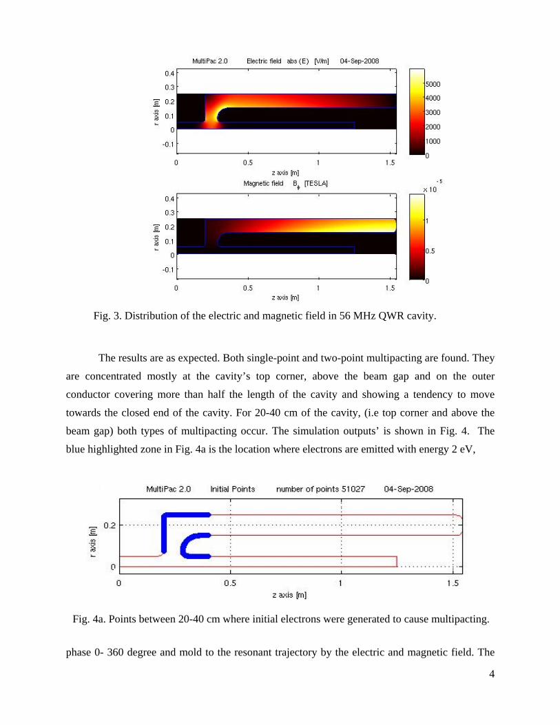
Fig. 3. Distribution of the electric and magnetic field in 56 MHz QWR cavity.
The results are as expected. Both single-point and two-point multipacting are found. They
are concentrated mostly at the cavity’s top corner, above the beam gap and on the outer
conductor covering more than half the length of the cavity and showing a tendency to move
towards the closed end of the cavity. For 20-40 cm of the cavity, (i.e top corner and above the
beam gap) both types of multipacting occur. The simulation outputs’ is shown in Fig. 4. The
blue highlighted zone in Fig. 4a is the location where electrons are emitted with energy 2 eV,
Fig. 4a. Points between 20-40 cm where initial electrons were generated to cause multipacting.
phase 0- 360 degree and mold to the resonant trajectory by the electric and magnetic field. The
4
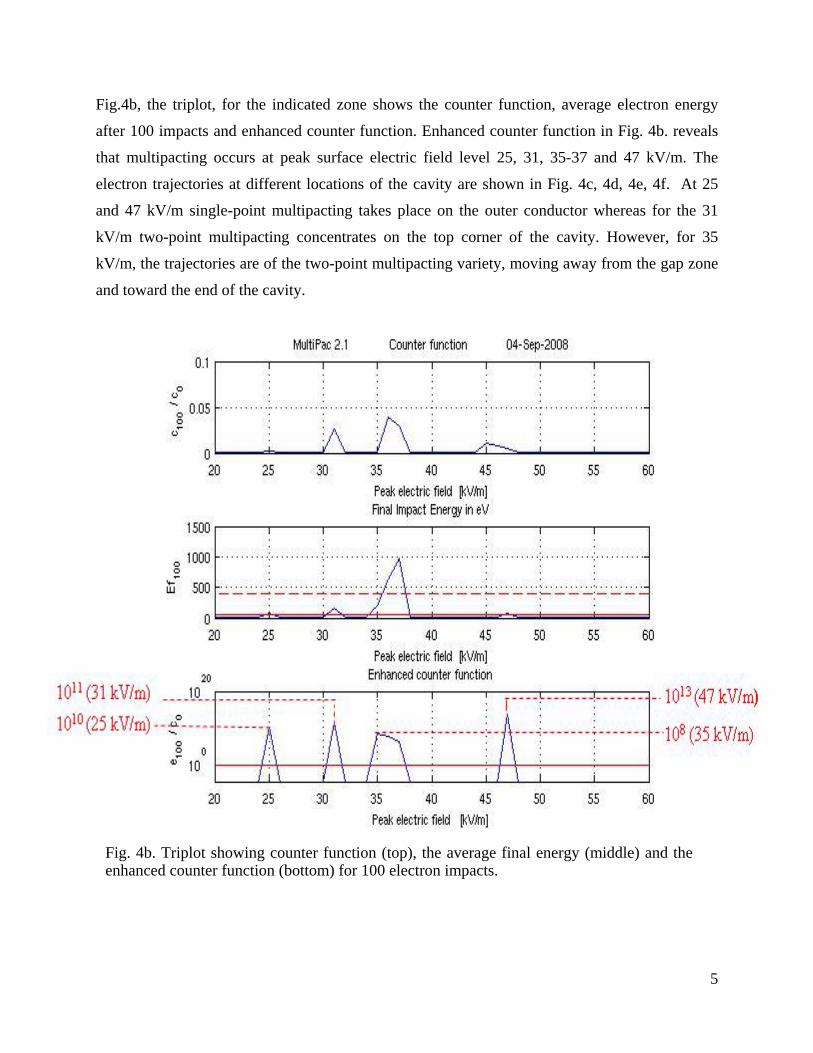
Fig.4b, the triplot, for the indicated zone shows the counter function, average electron energy
after 100 impacts and enhanced counter function. Enhanced counter function in Fig. 4b. reveals
that multipacting occurs at peak surface electric field level 25, 31, 35-37 and 47 kV/m. The
electron trajectories at different locations of the cavity are shown in Fig. 4c, 4d, 4e, 4f. At 25
and 47 kV/m single-point multipacting takes place on the outer conductor whereas for the 31
kV/m two-point multipacting concentrates on the top corner of the cavity. However, for 35
kV/m, the trajectories are of the two-point multipacting variety, moving away from the gap zone
and toward the end of the cavity.
Fig. 4b. Triplot showing counter function (top), the average final energy (middle) and the enhanced counter function (bottom) for 100 electron impacts.
5

Fig. 4c. Electron trajectory in single-point multipacting at 25 kV/m. The top figure represents the
trajectory of the electron in (r, z) coordinates, the middle one is an expanded plot of a part of the
top one, and the bottom plot illustrates the electron trajectory in (r, t) coordinates where t is the
time in periods. The circles indicate the impacts on the walls of the cavity.
6

Fig. 4d. Electron trajectory in two-point multipacting at 31 kV/m.
Fig. 4e. Electron trajectory in single-point multipacting at 47 kV/m.
7
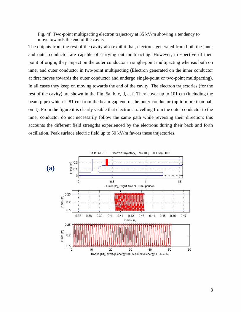
The outputs from the rest of the cavity also exhibit that, electrons generated from both the inner
and outer conductor are capable of carrying out multipacting. However, irrespective of their
point of origin, they impact on the outer conductor in single-point multipacting whereas both on
inner and outer conductor in two-point multipacting (Electron generated on the inner conductor
at first moves towards the outer conductor and undergo single-point or two-point multipacting).
In all cases they keep on moving towards the end of the cavity. The electron trajectories (for the
rest of the cavity) are shown in the Fig. 5a, b, c, d, e, f. They cover up to 101 cm (including the
beam pipe) which is 81 cm from the beam gap end of the outer conductor (up to more than half
on it). From the figure it is clearly visible that electrons travelling from the outer conductor to the
inner conductor do not necessarily follow the same path while reversing their direction; this
accounts the different field strengths experienced by the electrons during their back and forth
oscillation. Peak surface electric field up to 50 kV/m favors these trajectories.
(a)
Fig. 4f. Two-point multipacting electron trajectory at 35 kV/m showing a tendency to move towards the end of the cavity.
8

(b)
(c)
9

(d)
(e)
10

(f)
Fig.5. Electron trajectories for peak surface electric field (a) 36kV/m, (b, c) 40 kV/m, (d, e)
46kV/m and (f) 50kV/m.
3.1. Severity with electron impact more than 100: To assess the severity, the simulation was
continued for more than 100 electron impacts and with some trajectories continuing for 500,
1000 or more times. Enhanced counter function also increases significantly indicating an intense
electron cloud in the cavity (Fig. 6).
11
(a)

12
(b)
(c)
Fig.6. Some of the electron trajectories with 1000 impacts at peak surface electric field (a,c) 47
kV/m and (b) 31 kV/m.

4. Supression : The cavity cannot be operated safely in a storage ring when generating such a
large number of electrons, so this phenomena must be suppressed. We reasoned that the most
effective way to do so is by breaking the electron’s stable resonant trajectory, thereby preventing
its further multiplication irrespective of the cleanness of the niobium surface. While there are
several approaches to control it from outside of the cavity (For example: by applying DC field)
[2], due to complexity of the system and cryostat surrounding the cavity, they are not practical.
As a useful alternative, structurally modifying the cavity was considered, and hence simulations
were undertaken with various structures such as a bigger radius of the outer conductor (Fig. 7),
and also ripples pointing upward and downward direction in the outer conductor (Fig. 8).
Fig. 7. Multipacting with bigger radius (> 25cm) of outer conductor.
13

Fig. 8. Multipacting in the cavity when ripples point in the downward direction.
Among them the latter approach i.e incorporating ripples pointing in the upward direction seems
to be the most promising (Fig. 9).
Fig. 9. Ripple pointing towards upward direction.
14

To reduce the manufacturing costs, the ripples are optimized to a customary depth, width,
and ensure they are sufficiently separated. Also, they must leave sufficient space for coupler and
dampers at the end of the cavity. Ripple depth up to 2 cm were considered for ripple width 1-3
cm, with the maximum possible separation between the ripple. The simulation revealed that for
depth of 1 cm, the electron manages to have resonant trajectories in the ripple zone, moving
further and further, and multiplying electrons. Constraints on the material’s curvature also
prohibit shallow ripples. However, ripples of 2 cm depths are found to be most valuable. The
ripple’s width also is critical. A 1 cm wide ripple is not satisfactory as electrons can emerge from
it, whereas they undergo resonant oscillation inside a 3 cm ripple, and trapped there (Fig.10).
Though the energy of the electrons are only few eV less (δ > 1 at 55 eV) to have secondary
electron yield greater than 1, a little impurity in Niobium, may lead to multipacting. Hence, 3 cm
width should be avoided. However, 2 cm wide ripples are a good choice. Likewise it is essential
Fig. 10. Stable trajectrories of electrons inside a 3 cm wide ripple.
to determine the gap between the ripples. The stable trajectory of the electron is favored by
having gaps bigger than 2 cm. Fig.11 depicts the stable electron trajectories for a gap of 4 cm
between the ripples, whereas Fig.12 details the break in trajectory with 2 cm gap, even for 20
impacts.
15

Fig. 11. Multipacting trajectory with 4 cm gap between the ripples.
Finally, it was demonstrated that ripples 2 cm deep, 2 cm wide with a 2 cm gap between
them completely suppressed multipacting in the cavity.
16
Fig. 12. Discontinuity of the resonance electron’s trajectory with gap 2 cm between ripples, even for 20 impacts.

17
5. Test of ripple structure enhancing secondary yield: To account for a possible stronger
multipacting, due to any type of niobium poor surface conditions, the cavity with the ripple
pattern was tested with twice the value of secondary yield of electron. The region of δ larger than
one in this simulation extended and widened from 54 -1554 eV to 25 - 4105 eV. No
multipacting level was found even under this large secondary emission coefficient. This confirms
the robustness of the cavity with ripple against multipacting. Thus, in conclusion, the ripple
pattern of 2 cm deep, 2 cm wide with a 2 cm gap in-between was adopted for fabricating the
cavity.
6. Conclusion: The 2D simulation revealed sever multipacting in 56 MHz QWR. We also show
that multipacting can be eliminated in this cavity by structurally modifying its walls. Since the
cavity is equipped with a coupler and dampers, which were omitted in the simulation, a further
complete simulation is being carried out with a suitable 3D code to confirm the parameters for a
multipacting free cavity revealed by this 2D code.
References:
[1] A.J. Hatch et. al, Phy. Rev. 112 (3) (1958) 681
[2] H. Padamsee, J. Knobloch, T. Hays. RF superconductivity for Accelerators.John Wiely and
Sons Inc.
[3] http://www.bnl.gov/cad/ecooling/docs/PDF/56_MHz/Ben-Zvi.pdf
[4] http://conference.kek.jp/SRF2001/FA001.pdf