multi frequency test equipment ztek 75302 1 3—3 3—4 3—6 3—12 3—19...
TRANSCRIPT

MULTI FREQUENCY TEST EQUIPMENT
ZTEK 75302
EL

__
__
_
-_
__
__
__
__
_
LL
LU
H U,
H
C 1 m 0
C m z0
C
0 C -ci
-1

ELMCOflNHAGEN CENMAflK ELMU
COPZH.6EN DEU*
CONTENTS
1. INTRODUCTION 1-1
2. GENERAL DESCRIPTION 2-1
3. DETAILED DESCRIPTION
3.1 Printed Circuit Board
32 II
3 3 U II II
3 4 II II II
3 5 II U
3 6 U H
37 II II II
3 8 II II
39 II II U
3 10 II II II
3.11 U IS II
4. TROUBLE-SHOOTING, PERFORMANCE CHECK
AND ADJUSTMENT
Trouble-Shooting
Performance Check
Adj ustment
3—1
PA
PB, PC
PD
PE, PF
PG, PH
PJ
PK, PL
PM, PU
PP
PR, PS, PT
PN
3—1
3—3
3—4
3—6
3—12
3—19
3—20
3—23
3—27
3—29
3—31
4—1
4—1
4—3
4—5
4.1
4.2
4.3
5. REPLACEMENT PARTS 5-1
187—1179 III ZTEK 75302

ELMI ELMUCOPENHAGEN GENMAPA COPENHAGEN ALNUAPO
1. INTRODUCTION
The object of this manual is to describe,
J in detail, the hardware of the MultiFrequency Test Equipment ZTEK 75302.
The description concentrates on:
* Function
j* Diagram
F * List of components
* Location of components
[ The last sections give a brief descrip—tin of trouble-shooting and adjustmentprocedures.
For specifications and operation, see
the ‘Operator’s Manual’
]]
]
159—1179 1—1 ZTEK 75302

IJ
2 GENERAL DESCRIPTiON
The instrument comprises two features:
The GENERATOR TEST unit comprises a
balanced input selector and an accurate
frequency and level measuring circuit.
The measurable input signals cover the
range of the multi frequency signalling
tone generators.
The RECEIVER TEST unit comprises an
] accurate programmable two-tone generator
and a function and time measuring cir—
J cuit. The two—tone generator provides
a pulsed orcontinuous signal output,
j which is fed into the tone receivers of
the system being tested. The response
t — of the receivers is recorded by the
I measuring unit, which returns the rsult
as a functional test, an interruption
J test, or an operation time or release
time measurement.
The RESULT is presented on the RESULT
display, which includes a real-time dis
play of the receiver test input. If ac
tivated, the printer returns the result
together with the parameters.
The PARAMETERS, which are needed to en
able the test procedure, are loaded into
the MFTE by means of the keyboard. Each
test requires a different number of
parameters. The MFTE indicates the
appropriate parameters by flashing the
parameter display or keys, thus opti
mizing the parameter input sequence.
The test procedure is externally program
mable through the IEC—Bus interface.
Fig. 2.1 Functional Block Diagram.
d
HI
I
GENERATOR TEST enabling measurement of frequency and level of a generator (tone sen
der).
RECEIVER TEST providing functional test and reaction time measurement of a single re
ceiver or a pair of receivers (tone receivers)
I]II
I
Ij Input Generator test
160—1179 2—1 ZTEK 75302

ELMICOPENHAGEN OENMArnE
The MVfE is based on INTEL’s 8085 micro
processor, which controls all functions
of the instrument, and comprises the fol
lowing functional blocks:
* Microprocessor
* Program and Data Storage
* Receiver Test
* Generator Test
* IEC—Bus Interface
* Display and Keyboard
* Printer
* Power Supply
See the block diagram, fig. 22.
The microprocessor controls the exchan
ge of data with another block by means
of:
* data bus
* address bus and
* control bus
The control bus consists of control lines and selection lines.
Microprocessor clock for synchronization
of functions.
Data on data bus to be interpreted as
address byte A7-A0.
Unit addressed allowed to provide the
bus with data.
Unit addressed allowed to read data
from the bus.1ddress bit No. 13.
Selects data storage (1 k RAM).
Selects input of Receiver Test Input
and output of data for the printer.
Selects output of frequency for oscillator 1.
Selects output of frequency for oscillator 2.
ELMICOPENHAGEN OENUARK
TO SIGNIFICATION
Receiver Test,IEC-Bus,Display andKeyboard,Printer
Display andKeyboard
Resetting of internal functions:.
Program anaData Storage,
Receiver Test,IEC-Bus,
Display andKeyboard,
Printer
Data Storage
Receiver Test,
Printer
Receiver Test
Receiver Test
Receiver Test Selects output of attenuation for oscillator 1.
ZTEK 75302 2—2 161—1179

ELMICOPENHAGEN DENUANA
MEASHI
IECADR
IECBUS
The program and data storage contains:
14 k bytes program storage (PROM) and
]. k bytes data storage (RAN).
The receiver test contains 1) a two—to
ne generator with attenuators and an
output amplifier and 2) Test Inputs
from the tone receivers.
The two—tone generator forms digitally
two tones, whose frequencies are set by
the microprocessor. The two digital to
nes are converted into independent ana
log signals, which are attenuated by a
value set by the microprocessor. The
two analog tones are added in the out
put amplifier. An auxiliary signal may
be added too. The two tones (and the
auxiliary signal) are turned on/off by
the microprocessor, whereby two—tone
bursts are sent.
Test Inputs are through-inputs to the
microprocessor, which is the measuring
unit.
All time relations are controlled by
the microprocessor by means of a 4 kHz
clock, which gives an accuracy of
measurement of 1/4 ms.
The generator test contains circuits
for measuring the frequency and level
of the tone selected by the input se
lector circuit. The further processing
of the results of measurement is ef
fected by the microprocessor.
CONTROL TO SIGNIFICATION
LINE
A2 Receiver Test Selects output of attenuation for oscillator 2.
BURST Receiver Test Sets pulse/pause function.
GENIN Generator Test Selects output for Generator Test Input Selector.
Generator Test Selects input of frequency or level measured.
IEC-Bus Selects input and output of data for IEC-Bus
Interface.
CS1 Display and Selects input and output of data for
- Keyboard Display and Keyboard.
CS3
PRENAB Printer Causes printing to start.
RESET IN Microprocessor Forces the microprocessor to resume its
starting position.
INTTIM Microprocessor Timing signal for controlling duration of
tone bursts.
INTBUS Microprocessor IEC—Bus Interface has data for microprocessor.
INTKEY Microprocessor A key has been activated.
162—1179 2—3 ZTEK 75302

ELMI ELMIICO.ENAGefri OE3MA
COPE$Afle ONU*$Iç
The display and keyboard unit consistsof 1) control and driving circuits forcontrolling outputs to displays andLEDs and 2) a control circuit for controlling the input of a pressed key.Inputs and outputs are interpreted bythe microprocessor.
The printer contains, besides themechanical printer, a control circuitfor printing. Exchange of data andtime relations are controlled by themicroprocessor.
The power supply contains conventionalcircuits for generating +15 V, —15 Vand -30 V. +5 V is generated by aSwitch-Mode Power Supply.
The block diagram (fig. 22) shows howthe functional blocks described aboveare related to each other. The physicallocation on printed circuit boards isindicated by means of capital lettersin the bottom left-hand corner of eachblock.
F
r
Lr
CCL
ZTEK 75302 2-4 163—1179

ELMICGPENHAGEN DENMARK
RESETA13
ALE
1RDWR
PK
Display
PL ]II
I1 :‘‘‘
\?(ecei’’et TeI\\% Output _)
_jESET
z
IwU)
Indicates anatog tines
PX indicates the printedcircuit board.
Address Bus
Microprocessor
PGInterrupts
A13
16k IProgram Storagel
(PROM) IPH IF11
-;UC
•T2C0U
1kData Storage
(RAM)
enabLe
PHI
cr
U)
z
4
>-Ui
zI—
I—
Disptcy & Keyboard
Controt and interface
PL • PG enable
I I
RESETA13WR
pRDCLK
Printer
PRE NABenabte
RESET
Printer Interface A13
RAM 1enabLeALE
P]
Data Bus PN
0II
Control Lines
IECAD1IEC BUS,ALERESET
I
Power SuppLy
÷sv Switch Made
lLPowerSupplyf
+15V—15V I_3olTrafo module
I RegulatorsPR.PS
IEC—BusInterface
enable
PM
11
I—U)
D UU)C
CNUU)C
C)U)C
UU)C
;ii
iLi
‘Ii
‘Ii
Iii
ri
1
ower
II— l1< 1<
Receiver Test
I
________
6kHz I I Oscillators ttenuatorsI
—I CLock (dual)
______
(dual) IPD.Pi PEPF
________ _________
PB,PC
Test
___________
I’! I I
______________________
I Ill
J
I Input ‘Burst Control’
I 32dB Atte— II nuators(dual)I
& LOutput AmpLiI
______________________
_________
I IPA fier
JL
ELMICOPENHAGEN DEUMAPE
ZTEK 75302
IEC —BusAddressSwitches
MEA SH I
MEASLOI
MEASLOI1
[ Power
zzUi0
I—
Generator Test
,Frequency I I LevelMeasurement J Measurement
.IPD Ilpo
InputSelector &
_____
__________
AmplifierPA PD
jEC-Bus D
187—117 9
(Receiver TeN (ie Burst N\ Input ] 14.duIationJ
Fig. 2.2 Block Diagram
LLJ800R Impedctn
1160CR
__ __
Aux. InputSignal
2—5
11(Generator Tei‘4%_
lnputJ
Input.Impedance
15V
i 60k
1600R

L
H
ELMICOPENHAGEN DENMARK
3, DETAILED DESCRIPTION
The following pages describe, in detail,
how the functional blocks work.
The description is based on the division
into printed circuit boards. Consequently,
the description of each board may include
parts from several functional blocks.
3,1 PRINTED CIRCUIT BOARD PA:
Generator Test Input!
Receiver Test Output
The board PA comprises two parts: the
Generator Test Input and the Receiver
Test Output.
The generator test input consists of an
input selector which passes on one of
six balanced input signals, or the
auxiliary signal, to the balanced input
transformer. After being transformed,
the signal is low-pass filtered and
passed on from the board PA to the
measuring circuit on the board PD.
ELMUCOPENHAGEN DENMARK
The data latches 1C4 and 1C5 contain
information on the generator test. The
three least important data bits - D0
and D2 - select the input wanted ‘by
means of the decoder 1C6, the relay dri
vers 1C7 and the relays RE1-RE7. During
switch-on of power, the circuit R9, C3,
D2 ensures that the decoder is disabled,
until the right data has been written
out.
The data bits D3, D4 and 0 are control
signals for the measuremen and are
passed on direct to the board PD. The
connection of the 6002 relay REB is
controlled by the data bit D6, depen
ding on the position of the rear—panel
switch 40 / 600Q. If the switch is
at 0 V (the 600Q position), D = 1 will
cause a 604S2 resistance CR2) o lie con
nected parallel across the transformer,
thus creating an input impedance of
600c2. The microprocessor uses this pro
cess, when selecting the right input
for the following two purposes:
1) In the case of auxiliary input
measurements, the input is already
terminated by 6001. RE8 must,
therefore, be disconnected during
AUX. SIGNAL
AUXIN?.
6 INPUT
CHANNELS
INPUT )SELECTOR
600 Q
fl—I
INPUT TRANSFORMER
GTEST.INP.
\I (PD)
20kHz
IC 1
ZTEK 75302
_____ ________ _____________________
LOW-PASS FILTER
l—OUT—OF—7 [600 2
DECODER l5T0R
I c4- I c7
4 DATA BUS 3,Fig. 3.1 Block diagram of Generator Test Input.
3—1164—1179

ELMICOPEWHGEN DENMARK
measurements, irrespective of the
position of the switch.
2) When changing over from one input
relay to another, there is a risk
of causing damage to the relay
contacts, if RES is connected at
the same time as ringing voltage
(lb Vrms, 25 Hz) is applied to an
input. The microprocessor, there
fore, ensures that RE8 is discon
nected during the change—over.
The input wires to the balanced trans
former contain two resistors, R30 and
R31, which attenuate the unintended
oscillations (approx. 10 Hz) which may
occur when TR1, C2 is connected to a
generator with low impedance and DC
offset.
R4 ensures a uniform input impedance in
the frequency area 200—6000 Hz, whereas
differences of performance of the trans
former may lie adjusted by means of the
adjusting resistors RX1 or RX2.
IC1 functions as a low —pass filter
with an upper cut—off frequency of
approx. 20 kHz and is input-protected
by D3 and D4.
(PB)
(PB)
(PC)
(PC)
The receiver test output receives two
analog tones from the attenuators PB
and PC. Depending on the value of the
attenuation, both tones may be attenua
ted by 32 dB before being added in the
output amplifier. An auxiliary signal
from the rear panel may be added to the
tones. From the output amplifier, the
signal is sent to the line via the ba
lanced output transformer.
The 32 dB attenuators are controlled
by the relays RE9 and RE1O. The
auxiliary signal is controlled by the
electronic switch 1C3, which ensures
that the input impedance of the signal
is correct, no matter whether the sig
nal is sent to the output amplifier or
not.
1C2 functions as a summation amplifier,
which sends the signal to the current
amplifier T3. The amplification at this
stage is set by the potentiometer P3.
T2 is a constant-current source (approx.
60 mA) for T3, which is protected
against overvoltages from the transfor
mer by means of D9.
The output transformer TR2 has two in
puts: one for an output impedance of
Fig. 3.2 Block diagram of output amplifier.
ATT3 2dB 1
AUXINP
AUX.SIGNAL 1C3
ZTEK 75302 3—2165—1179

ELMILOPNH8GE M flENUAfW
60O2 and another for an output impe
dance of 800c2. The input to be used is
selected by the relays RE11 and RE12.
The value of the output impedances are
determined by R27, P1 (600S2) and R28,
P2 f800c2), whereas the relation between
the two output voltages is determined
by RX3.
(PE)
(PE)
PE)
ELMHCOPENHAGEN DENMOAK
3,2 PRINTED CIRCUIT BOARDS PB) PC:
Filter and Attenuator
ATTOUT
(PA)
ATT32dB
(PA)
The dependence of the
of the transformer on
is compensated for by
R32.
copper windingsthe temperaturethe NTC resistor
The MFTE has two filter and attenuator
boards, one for each tone. The tone
is received from the digital oscillator
as negative half—waves in the form of
quantized current, which is converted
into quantized voltage, Every second
half—wave is converted into a positive
half-wave (controlled by the signal
SIGN), whereupon the quantized sine
SIGN
‘Cl
1C3 — 1C4
LOW-PASS FILTER
4th ORDER
ATTENUATORS
OS CON
FOR TURNING OSCILLATOR
ON/OFF
FOR SELECTION OF
32dB ATTENUATOR ON PA
ICl2—1C15
Fig. 3.3 Block diagram of filters and attenuators.
166—1179 3—3 ZTEK 75302

ELMICOPENHAGEN DENUAPH
tone is sent through two 2nd orderButterworth low—pass filters connectedin series, which remove the samplefrequency. Depending on the attenuationvalue set by the microprocessor, thesine tone is attenuated by the attenuators (note that the last 32 dB attenuator is located on the board PA).
IC1 and Ri form the current-to-voltageconverter, where Ci removes the spikeswhich may occur in connection with thequantization of the tone by the D/Aconverter.
By means of the switch T2, 1C2 formsan amplifier capable of amplifyingby +1 (T2 is open) or -1 -R3/R2fT2 is closed). The DC—offset of IC1and 1C2 can be adjusted by means ofP1 so as to minimize the jump betweenpositive and negative half—waves.
1C3 and 1C4 both form a 2nd orderButterworth low-pass filter with a cutoff frequency of 20.5 kHz (=/21rR9C2),
which means that the sample frequency
(65.5 kHz) is attenuated by 40 dB. Theattenuation of the highest possible
tone frequency (4095 Hz), however, isonly 0.0001 dB the attenuation of256 Hz.
The attenuators are constructed as voltage dividers which may be connected bymeans of relays. Note that the 64 dBattenuator is formed by two 32 dBattenuators, one of which is located onthe board PA. This is to avoid theintroduction of noise in connectionwith large attenuations.
33 PRINTED CIRCUIT BOARD PD:
Generator Test
The generator test board measures thelevel or frequency of the analog signalfrom the board PA.
Thi,s function is divided into two partsas follows:
1) an analog part where the level ofan analog signal is convertedinto a frequency, and
ELMICOPENHAGEN OENUAHN
1SUUL
(PA) ENABLE
Fig. 3.4 Block diagram of analog part.
ZTEK 75302 3—4 167 —ll7

hXUi
2) a digital part consisting of a
period—measuring unit.
The object of the analog part is to
convert the level and frequency of the
analog signal into square—wave signals
with frequencies proportional to the
level and frequency just mentioned.
The analog signal is sent through an
amplifier which is set at 0 dB or 25 dB,
depending on the level of the analog
signal. After being high-pass filtered,
the signal is sent to a rectifier and a
Schmitt-trigger. The latter converts
the analog signal into square—waves
with the same frequency as the signal.
A low—pass filter smoothes the positi
ve half—waves from the rectifier so as
to produce a Dc-voltage.
Passing through a voltage-to-frequency
converter, the Dc—voltage is converted
into square—waves with a frequency
proportional to the level of the analog
signal.
1c2 is a 2nd order high—pass filter
with a cut-off frequency of 40 Hz
(=V’/2irR9c3), the purpose of which is
to cut off the Dc from ici and at the
same time prevent low—frequency oscil
lations from the input transformer
from getting any further.
1c7/1 is a comparator, which functions
as a Schmitt-trigger for the analog
signal. Its output is a square—wave
signal with the same frequency as the
input signal. The Germanium diode D4
prevents the input voltage from fal
ling below -0.3 V.
ic4 and 1C3 together function as a
full—wave rectifier. In the case of
negative half—waves, 1C3 will force
(by means of D2) the 1C4 +input to
earth, and 1C4 will function as an
inverting amplifier, thus causing the
1c4 output to appear with positive
half-waves. In the case of positive
half-waves, the 1C3 output will follow
the signal at the 1c4 +input, and D2
will block the current. In this case,
1c4 functions as a non—inverting am
plifier, and the positive half-waves
are passed direct through 1c4. Dl
ensures that the differential voltage
between +input and —input does not
exceed 0.6 V (the highest permissible
differential voltage is 7 V).
ics is a 2nd order low-pass filter
with a cut-off frequency of 70 Hz
(=1/2rrRl7c5), which smoothes the posi
tive half-waves to a Dc-level with a
maximum ripple of 2% at 200 Hz. The
final smoothing occurs in R21, c7
where the ripple is max. 0.1% at
200 Hz. The 2nd order filter has a
double pole at 70 Hz, which ensures
minimum ringing when a signal is
applied. Thereby the amplification
control 1c7, I9 is prevented from
oscillating.
The cut—off frequency was chosen at
the value (70 Hz) giving the shortest
possible signal delay (30 ms).
Ic6 is a precision voltage—to-frequency
converter, which gives a frequency pro
portional to the input level. The am
plification of this stage is regulated
by means of P3.
The amplification control 1c7, ic9
consists of a comparator and a f lip—
flop.
The comparator controls the amplifi
cation of the id input signal, thus
ensuring that the level of the 1C5 out
put signal will be 0—25 aB. The f lip—
flop 1d9 remembers the position of
1c7. By means of the disable signal
GENATT, the flip-flop is prevented from
changing position during a measurement.
Ic7/4 indicates whether the input sig
nal is too low for measurement
(<—25 dBu).
The digital part consists of a period-
measuring unit, which measures the time
it takes for the square—wave signal
produced in the analog part to traverse
64 periods. The further calculation of
the correct level or frequency is made
by the microprocessor.
A measurement starts by the signal
START cONy, clearing the start/stop
flip—flop 1d14/2, the overflow f lip—
flop 1d14/i, the 8 bits counter 1d12—13
168—1179 3—5 ZTEK 75302

-
ELMICOPENHAGEN DENMARK
ELMICOPENHAGEN DENMARK
L
-i-u‘LEVEL’
JL
‘I,mL
EELLI
Fig. 3.5 Block diagram of digital part.
E
and the 20 bits counter 1C15-17. When
START CONy, disappears, the first pul
se from IC11 will load 1C12,13 with
the number 64, and the 20 bits counter
will be enabled. The counter 1C12,13
will count up to 128, whereupon the
start/stop flip-flop 1C14/2 is set at
1 thus disabling the 20 bits counter.
The latter will then have counted the
number of 3.2 MHZ clock pulses during
64 periods of the input signal.
The overflow flip-flop 1C14/1 will
signal, if the frequency of the input
signal is too low.
Oscillators (dual)
The boards PE and PF form a two—tone
digital frequency synthesizer, both
tones being generated as independent
digital waveforms.
Principle
Within a read-only-memory (ROM) the
equivalent of 216 words are stored,
corresponding to equispaced samples of
a sine wave taken over exactly bne
r
Fig. 3.6 Block diagram of oscillator principle.
F
4kHz
1c12—iCl3
IC 14
‘FREQUENCY’
FINISHED
6.400MHz
•11C22—1C23
DATA BUS
3t4 PRINTED CIRCUIT BOARDS PE, PFC
ROMADDRESS
STEPPED FILTERED
SINE WAVE SINE WAVE
FREQUENCY WORDSAMPLE
CLOCK
ZTEK 75302 3-6 169—1179

ELMHCOPENHAGEN DENMARK
waveform cycle. The ROM is addressed
by an accumulator whose 16—bit contents
at any instant correspond to a sine wave
angle. On each clock pulse, the accu
mulator is incremented by an amount
propotional to the desired output
frequency. This is accomplished by
adding the increment to the previous
word and storing the result.
The output of the ROM is applied to a
digital—to—analog converter, generating
a sampled—and—held stepped sine wave as
the accumulator steps the ROM through
the indicated addresses. Because the
stepping frequency is many times higher
than the sine wave frequency, low—pass
filtering easily removes the steps to
give a clean sine wave.
Clearly, the output frequency is pro
portional to the speed with which the
addressing advances through the sample
table stored in the ROM. Higher frequen
cies thus have fewer samples per cycle.
To simplify the filtering, the clock
rate was made high enough (65.536 Hz)
to generate about 16 samples per cycle
at the highest output frequency
4.095 Hz). The clock rate is exactly
the number of stored samples ( 216) so
the lowest output frequency would be
1 Hz and all other frequencies are mul
tiples of 1 Hz. The low end of the in
strument’s range, however, is restric
ted to 256 Hz.
In practice, storage of 65.536 (216)
sine wave samples is economically
impractical. An immediate four-fold
reduction is achieved by storing samp
les for one quadrant only, and reusing
the data appropriately to derive the
other quadrants.
A further reduction of significant
proportions is achieved by use of the
relationship (valid for small B):
sin(A+B) sinA + cosAsinB
Relatively few values of A are used to
give coarse angular resolution and
small values of B can increment the
angles between values of A. The ROM
stores 64 magnitude values of sinA
equispaced throughout a quadrant which,
of course, also gives 64 magnitude va
lues for cosA. Then the ROM has 64
values for sinB magnitude but since
negative values of B can be used, these
only have to have a range sufficient
to interpolate half-way between the
values for A. Sign information is
supplied by the accumulator register.
Thus, the real—time calculation of
each sample value from reduced sine
function information enables a ROM of
only 64x12 bits to be used.
The principle of calculation is shown
in fig. 3.8. Bit 15 (sign) indicates
whether the value calculated is posi
tive or negative.
Bit 14 indicates whether cosine or si
ne of the angle should be calculated,
the sines of the quadrants being rela
ted as follows:
sin (ff/2+X) = cosX and
sin (rr+X) = —sinX
Bit 7 indicates whether angle B
should be added or subtracted.
(Note that the ROM contains sinA and
sinB. CosA and cos(A+B) are found by
complementing the address bits of A and B).
2
BIT 115114 113 112111110 I 918 1 16 lIl 312 Iii oJ
QUADRANT A B
SIGN -*SIGN OF ANGLE B (0 + , 1 -)
Fig. 3.7 Accumulator Register.
170—1179 3—7 ZTEK 75302

tv -
NOENUOH E LM ICOPENHAGEN OENMAHE
C
_________________
C
ACCUMULATOR REGISTER 16 3115—14 13—8 7 6—1 0
QUADRANT I
_____
I IGNORE BIT 0CONTROL
SIGN.B
BIT 14COMPLE- COMPLE-
BIT 14
A (COARSE) B (FINE)
TIMING MEMORY ADDRESS DECODER
6 BITS
tsinA cosA sinB
9 BITS 4 4 BITS
4 x 4 BITSMULTIPLIER
4 BITS (MSB)
2s BIT 14
BIT 7
9 BITS ADDER I8 BITS
D/A J
EFig. 3.8 Block diagram showing the principle of calculation of sinA+cosAsin3.
ZTEK 75302 3—8 171—1179

ELMICOPENHAGEN OLNUARK
circuit. Calculations are controlledby time signals. Interim and finalresults are stored in registers.
QD = 0: OSC1
1___ QD02
Fig. 3.9 Time diagram for calculation of sinA4cosAsinB.
The board PF contains registers for thetwo oscillator frequency words, the 16bits adder, the accumulator registerand the memory address decoder.
The frequency words of the two oscillators are written into IC1-6 from thedata bus. IC1-6 include output disabling features, and data on the A—buscan thus be controlled by means ofQo and rj. When QD = 0, the frequencyword of OSC1 will be on the A-bus. Data are written into 1C7-1C14 from the
output of the 16 bits adder, when sineof the accumulator register word(= adder output) has been calculated,i.e. the input takes place at the endof the period QD/ (by means of thesignal Q3/Q3). 1C7—14, too, includeoutput disabling features whereby dataon the B-bus are controlled. Theaddress bits for the ROM are decodedin the complement/no complement circuit 1C19-22, and addition/subtractionof cosAsinB is indicated as follows(116)
ELMICOPENHAGEN GENUAPH
Hardware
The boards PE and PF contain two digital frequency synthesizers, which,however, use the same calculating
[J
I
T0— I I Calculation of sin3
T6 ......fl____________ Storage of sin3
T1 J [ I 1 Calculation of cosA
‘Ir; Storage of cosA
T3— I I I L Calculation of sinA and sinA+cosAsin3
Q Storage of result for OSC1
Q Storage of result for OSC2
172—1179 3—9 ZTEK 75302

I
ELMICOPENHAGEN DENUARK
ELMICOPENHAGEN NEUMANN
C
Fig. 3.10 Block diagram of board PF.
OSc 2
,4,6
1C15—18
6 BITS
ICl9,2o
S15
(P2) (PE)
1c23 ,24
Y 6 BITS
-—1 fl173—1179

ELMICOPENHAGEN OGNUAflA
BIT 154 CPF)
6 BITS (MULTIPLEXED)
I C7 —9
1C12
IC 13
Si nB
QD 4
QD 4
Q3 4-
1
[]
LiJ
TOCONTROL &
(PB)
Ti
(PC)
T014-
T1 4
Jici—6,2i
18.388.608Hz
OSC1OFF
IC 15—18
8 BITS
DA1
1C22
(PB)
IC 23
DA2
(PC)
Fig. 3.11 Block diagram of board PE.
174—1179 3—11 ZTEK 75302
ELMICOPENHAGEN OEUUARK
Complement of bits 13—8:
T1 1: Calculation of cosA
T1 0: Calculation of sinA
C = Complement
0 = No complement
Complement of bits 6-1 and cosAsinB
(= subtraction order):
bits 6—1 116
57b;4\__0 1
0 CO
1 CO
The address bits 6-1 (during period T0)
or 13-8 (outside period T0) are selected
by the multiplexers 1C23-24.
The board PE contains the circuit for
calculation of sinA+cosAsinB, registers
and D/A—converters.
sinB. The four most significant bits
of cosAsinB are taken from the 4x4
bits multiplier 1C13. Depending on 116,
the result is complemented in 1C14.
1C16 (4 bits adder) will increase the
result by the least significant bit of
cosAsinB and add the least significant
bit of sinA. The result is then added
to or subtracted from the 8 bits sinA
in 1C17 and 1C18. The final result is
stored in 1C19 (OSC2) or IC2O (OSC1)
and is D/A-converted in 1C23 and 1C24
respectively.
The D/A-converters are supplied with
reference current from 1C22. The maxi
mum values can be adjusted bu means of
P1 and P2. The tones can be turned off
by means of the signals OSC1OFF and
OSC2OFF respectively.
The frequency accuracy is set by the
crystal oscillator, and control and
timing signals are generated by IC1-6.
The sine half—wave sign is written in
to 1C21.
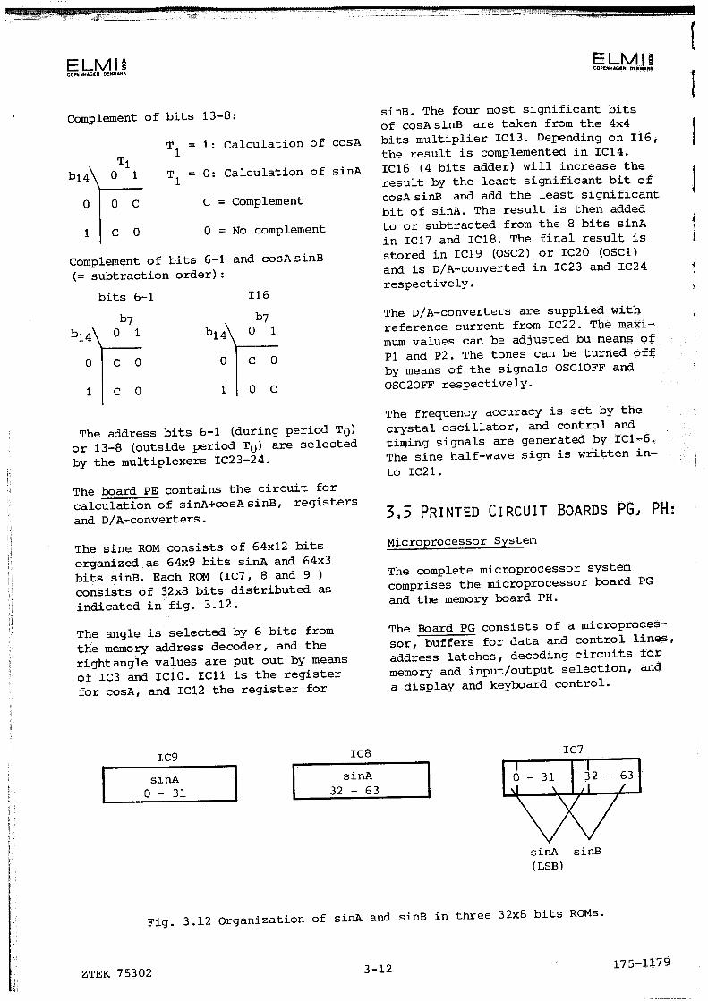
The sine ROM consists of 64x12 bits
organized as 64x9 bits sinA and 64x3
bits sinB. Each ROM (1C7, 8 and 9
consists of 32x8 bits distributed as
indicated in fig. 3.12.
The angle is selected by 6 bits from
the memory address decoder, and the
rightangle values are put out by means
of 1C3 and IC1O. IC11 is the register
for cosA, and 1C12 the register for
1C9 ICS
Microprocessor System
The complete microprocessor system
comprises the microprocessor board PG
and the memory board PH.
The Board PG consists of a microproces
sor, buffers for data and control lines,
address latches, decoding circuits for
memory and input/output selection, and
a display and keyboard control.
Fig. 3.12 Organization of sinA and sinB in three 32x8 bits ROMs.
T101
ELMiCOPENHAGEN DENMARK
0
1
0 C
CO
b701
0
1
CO
OC
315 PRINTED CIRCUIT BOARDS PG, PH:
si nA0 — 31
S mA32 — 63
I C7
sinA 5mB
(LSB)
ZTEK 75302 3—12 175—1179

ELMHCOPE*IAGEN aEHMAHK
The microprocessor IC1 has control and
interrupt lines, whose functions are
described in section 2. The five control
lines CLK, RESET OUT, ALE, ö, and WR
are buffered by the driver circuit 1C7.
The data bus AD0-AD7 is buffered by the
bidirectional bus driver 1C5, whose di
rection is controlled by the signal 1D.At the beginning of the machine cycl
of the microprocessor, the data bus
will contain the S least significant
MEMORY SELECTION (PH)
address bits AD - A7 (ALE being active).
AQ -A7 are stored in the data latch
1C6, which means that 1C6 and 1C9 will
have 16 address bits at their outputs.
The decoding takes place in 1C12-1C16
according to the following memory map
I/o principle: input or output is in
terpreted as a memory address. The
microprocessor can address up to 64 k
bytes. The memory map therefore looks
as follows:
‘/0SELECTION
CONTROLAND
DO-D7
1C2—1C4ICS , IClo—IC1 1
TO DISPLAY FROM KEY3ORD
(PK,PL) (PL)
Fig. 3.13 Block diagram of board PG.
2
I
L
[]
PROGRAM MEMORY INPUT/OUTPUT
( PROM ) DEVICES
0 32( 34k 64k
DATA STORAGE
RAM )
Fig. 3.14 Memory map.
176—1179 3—13 ZTEK 75302

:z.r
ELMICOPE4HAGEN OEUM*flK
The memory addresses used are as
follows:
ADDRESS NAME
0000H - 3FFFH Program Memory C 16k)
RAMØ , RAM1
oscl/1
OSC2/ø
0SC2/1
MEASW/Ø
MEASW/ 1
DIS3D (8279,43)
Fig. 3.15 Memory Addresses.
The internal registers of the 8279-cir
cuits are addressed by means of A13 in
combination with one of the address
lines DIS1D, DIS2D or DIS3D.
The Input/Output selection signals
from 1C13 and 1C14 are of the same
duration as .B in the case of read—in
from inputs. In the case of write—out
to outputs, their duration is half a
ELMUCOPENUGEN DENMARK
The 8279-circuit is a programmable key
board and display I/o interface device.
The keyboard part provides a scanned
interface to a 64 contact key matrix.
The display part provides a scanned
display interface to a 16x8 bits ma—
t rix.
The 8279-circuit reads the keyboard by
scanning the RL-lines for ground level,
the latter indicating contact making.
The address of the active key (0—63)
is stored in an internal RAN, which is
accessable to the microprocessor. At
the same time, an interrupt signal
fINTKEY) is sent to the microprocessor.
The 8279-circuit automatically checks
for contact debouncing and 2—key roll
over.
Output to the display is controlled by
the scanning lines RS. The 8279-circuit
has an internal 16x8 bits RAM, which
can be updated by the microprocessor.
Data are written out from the RAM to
the A- and 3-lines, 8 bits at a time,
the scanning ratio thus being 1:16.
After each write—out, the data are
, and t changes to a low state
usable for blanking of displays.
Input from the keyboard is read by 1C2
(8279,#1), the keys having the fol
lowing internal addresses:
Internal address Key function
Rec. Test Auto
Function
Interruption
C
CLK-period shorter than
in order that data hold
long enough for data to
into the CMOS-circuits.
tation is controlled by
Data Storage
;jj• This is so
time may bebe writtenThe signal du1C15 and 1C16.
OSC1/ø
CC
tI
GENIN
800011 — 87FFH
880011
8801H
8802H
8803H
8804H
880511
8806H
880711
8COOH
8C0811
8C1OH
8C1&
8C2811
9000H
940011
980011
f 2k)
MEASHI
ATT 1
ATT2
IECADR
IECBUS
PRENAB
DIS1D f8279,4#1)
DIS2D f8279,#2)
0
1
2
3
4
5
Hold
1
2
7.TEK 75302 3—14177—1179

Internal address Key function
6 3
7 A
8 Run
9 Operation Time
10 Release Time
12 4
13 5
14 6
15 3
16 STEP
17 Op. + REL. TIME
18 OP. - REL. TIME
20 7
21 8
22 9
23 C
24 AUX. Level
25 Frequency
27 Load
28 *
29 0
30
31 D
32 Gen. Test Auto
33 Level
41 Print
Fic. 3.16 Internal key addresses.
178—1179
L
LiL
L
L]
]HH
ELMICOPENHAGEN GENU000
3—15 ZTEK 75302

1C2 contains information for 32 dis
plays in the form of 4 bits BCD. For
each scan, two figures are read out,
one on the A—lines and one on the
B-lines. The displays are addressed as
follows:
Scan counter A B
0 Deviation OSC2(1) Freq. series (1)
1 Deviation 0SC2(O) Freq. series (0)
2 LEDS abs./rel. Oscillator 1 (3)
3 level (2) Oscillator 1 (2)
4 Level (1) Oscillator 1 (1)
5 Level (0) Oscillator 1 (0)
6 md. level 1 (1) Deviation OSC1 (3)
7 md. level 1 (0) Deviation OSC1 (2)
8 md. level 2 (1) Deviation OSC1 (1)
9 md. level 2 (0) Deviation OSC1 (0)
10 Pulse (2) Oscillator 2 (3)
11 Pulse (1) Oscillator 2 (2)
12 Pulse (0) Oscillator 2 (1)
13 Pause (2) Oscillator 2 (0)
14 Pause (1) Deviation OSC2 (3)
15 Pause (0) Deviation OSC2 (2)
Fig. 3.17 Display addresses in 1C2.
1C3 (8279,#2) contains information for
result displays, result LEDs, decimal
points of displays (whether to flash
or not) and LED5 (whether to flash or
not), which are addressed as follows:
ELMICGPENH4Q€ DENMARK
CICICi
HCEEECCCCUECCCCC
ZTEK 75302 3—16179—1179
r

U
r
LI
LI
-
v-I
LIrL]
5
for
1
= 2
= 3
= 4
= 5
= 6
= 7
for
1
2
3
= 4
= 5
AB = 1
= z
= 3
(4)
(3)
(2)
(1)
(0)
ACC.
4 3 2
keyboard LEDs:
LOAD
Gen. Test
Rec. Test
STEP/RUN
Gen. no..
Rec. Comb.
decimal points:
Frequency series
Oscillator 1
Level
md. level 1
Ind. level 2
Oscillator 2
Deviation OSC
Deviation OSC2
COPENHAGEN DENMARK
A B
Scan counter 3 2 1 0 3 2 1 0
LJVI ICOPCU0400 OENMAflK
Result
Result
Result
Result
Result
Hz
8
Remote
Flash
dBu ms
7 6
Gen Rep.no. cOmD.
information
AB
REJ.
1
result LEDs
result LED5
result LEDs
0
1
2
3
4
5
6
7
8
9
10
11
12
13
Flash information
AB =
180—1179 3—17 ZTEK 75302
ELMI£OPtHHACCN DENMARk
The board contains data registers for
the printer. The registers consist of
7 data bits for the printing head and
4 control lines.
The pulse/pause ratio of the Receiver
Test Output signal is controlled by
the signals MODOSC from the rear panel,
OSCON from the filter boards PB/PC and
BURST from the microprocessor.
The tones OSC1 and OSC2 and the AUX.
SIGNAL are set independently ON/OFF bythe Tone Burst Control 1C6. The inputsMODOSC1, MODOSC2 and MODAUX from the
rear panel are protected by means of
VTC-resistors and diodes and will
witstand voltages of up to 125 Vrms.
3,7 PRINTED CIRCUIT BOARDS PK, PL
The Input Detectors ICS—1C15 are window
comparators which are activated by
means of the reference voltage V+REF
and VREF, if the input voltage is
between -1.6 V and 1.6 V. In the case
of open input, the pull-up resistor
connected to +5 V will pull the input
out of the active area. The compara
tors are protected at the input by
resistors and a Zener diode. The value
of the latter was chosen so as to
achieve as little leakage current as
possible. The 16 detected input signals
are encoded by the priority encoder
IC1/1C4, which, by means of 1C2, shows
a binary figure 0-15. Out of 16 inputs
which may be active, the figure indi
cates the active one with the highest
number.
The multiplexer 1C3/1C5 chooses to show
either the binary figure from the prio
rity encoder or the real picture of
inputs 1—8. The multiplexer is control
led by the signal REC f1-OF-16) from
the rear panel.
1C7 (8155) contains three programmable
input/output ports, a progammable
timer and 1/4 k RAM. 1C7 is controlled
by the microprocessor. Port A is used
as input port for the 8 bits Receiver
Test Input signal from the multiplexer
1C3/1C5. Port B is used as output port
for data to the printer and Port C as
input port for data from the printer.
Some inputs and outputs are protected
against overvoltages from the printer
by means of diodes. This version of the
instrument does not use the 8155-timer.
As, however, this timer has a 4 kHz in
put signal, it may be activated. By
means of strapping, the timer’s output
signal TIMER OUT may be admitted to
INTTIM.
Display and Keyboard
The display board PK, the keyboard board
P1 and the interface circuits 8279 on
the board PG together form a complete
control and interface system for the
display and keyboard.
The board PK contains displays, result
LED5 and cathode drivers for displays
and LEDs.
The method of writing out data to dis
plays and result LEDs is decribed in
section 3.5 under Printed Circuit Board
PG. The scan counters from 8279, #1 and
**2 are decoded on the board P1 into
1-out-of-16 signals which drive the
common cathodes of the displays.
A— and B-data are decoded on the board
P1 into 7-segment signals, which, to
gether with decoded scanning signals,
give information to each individual
display.
The decoded scanning signal and the
A- and B-data are decoded in the NAMD
circuits. The information is passed on
to the result LEDs.
IC1—1C6 are cathode drivers capable of
yielding up to 1.5 A, which is the ma
ximum amount of current that can be
pulled through two displays (each con
sisting of seven segments and one deci
mal point) during the presence of a
scan value. The diodes Dl and D2 (LEDS
for ABSOLUTE and RELATIVE LEVEL) are
selected by means of segment_decoding
too.
1C43—1C52 select and drive the result
LED5 by means of the cathode driver
1C6 and data from the A- and B-data
buses.
1O 11Q
ELMICOPENHAGEN DENMARk r
t
tt

DISPLAYSEGMENT DATA
(PL)I
The result LEDs are gathered intogroups, each group sharing a feedingresistance. This is possible becauseonly one LED at a time of each groupcan light.
The decimal points of the displays1C7-1C37 may be made to flash bymeans of data from the board PL. Thisalso applies to the LEDs GEN.NO. andREC.COMB. (D17, D18).
Ti and T2 will cause the decimal pointof 1C41 of the result display to lightwhen the b— og c—segments light.
The board PL contains the keyboard,key LEDs, decoding for displays,decoding for key and result LEDs anddecoding for flashing of key LEDs anddecimal points of displays.
The procedures connected with input fromthe keyboard and output to displays, keyLED5 and result LEDs are described in section 3.5 under Printed Circuit Board PG.
The scan counter from 8279, #1 is decoded into 1-out-of-8, which is used inthe key matrix to locate the pressed key.
The same scan counter is decoded into
i-out-of-16, which is used on the boardPK for selection of displays. The A-and B—buses are decoded by separate7—segment decoders for the use of displays on the board PK.
The scan counter from 8279, #2 is decodedinto 1-out-of—16. The B-bus is decodedby a 7—segment decoder for the use ofthe five displays of the result display.
The A— and 3—buses are transferred tothe board PK and decoded for the useof result LEDs.
The eight highest values of the scancounter are used for writing flash information from the A— and B— buses intothe registers. The flashing is controlled by a 1 HZ oscillator, which turnsoff the registers for half the period.During the other half, the oscillatorallows the registers to be updated sothat the LED5 or decimal points selected will light.
The scan counter from 8279, t3 hasalready been decoded into i-out-of-4.The key LED5 may, therefore, be selected directly by the A- and 3-buses.
1C19 is a 3-to-S decoder for the key—
LZ L_IVI I SCOPLHCE” OENUAR
LED DATA
DECODEDSCANNING(l—OF—16)
(PL)
(FL)
I
Fig. 3.22 Block diagram of board PK.
184—1179 3—21 ZTEK 75302

(PK)
(PG)
(PG)
(PG)
(PG)
Fig. 3.23 Block diagram of Board PL.
ELMICOPENHAGEN DENMARK
crV[J
Ui
[J
KEYBOARD
(PG)
8279,# 1 1c31—1c32
(PG)
DECIMAL POINTS
IVERS >(PK)
ZTEK 75302 3—22 185—1179

J
I]ii
I]I
I
ELMIOPENHAAN DENMARk
board. The output selected goes low.If a key is pressed, the corresponding RL-line will go low therebyindicating the pressed state to the8279-interface circuit. The diodesD1—D6 will protect 1C19 if two ormore keys are pressed at the sametime.
1C26, 1C31 and 1C32 are 7—segmentdecoders with a constant currentoutput. They drive the display segments by means of the transistors Ti—T21 (120 mA/segment).
During change of data on the A- andB-buses, the displays are blanked bymeans of the -signal at the -in—put.
1C29, 1C30 and 1C25 are 8 bits addressable latches, which are used here as3—to—S decoders controlled by scancounters.
1C20, 1C21 and 1C22 are 8 bits addressable latches too, but are used for decoding of the B-bus. The input is selected by the 3—to—S decoder 1C24. TheBD—pulse is prolonged in 1C27 to 220usand is used as trigger pulse for thelatches. The flash information is written in by means of addressing on the3-bus.
1C20 provides the key LED5 with flashinformation, whereas the decimal pointsof displays receive information from1C21 and 1C22.
The decoding and driving of key LED5are effected in IC1—1C16. The LEDswhich can be turned on only one at atime share a feeding resistance.
The board PL also includes the RESETkey. The diodes D7-D9 cause the non-active high level on the RESET-lineto be rapidly reduced to 0 V when power is turned off.
The POWER key is a 5 V key which canturn on the power supply by means of asmall constant—on power circuit.
Note that displays and LEDs have a separate 5 V supply line.
186—1179 3—23
ELMUCOPENHAGEN DENMARK
38 PRINTED CIRcuIT BOARDS PM, PU
IEC-Bus Interface
The IEC-Bus interface board PM and theIEC-Bus connector board PU togetherform a complete interface system between the IEC—Bus and the microprocessor.
IEC-BUS
The IEC-Bus system is defined in detailby the IEC-publication: Standard Interface Systems for Programmable MeasuringApparatus, July, 1974. This standard isvery similar to the IEEE-standard488—1975.
The specification allows three basicfunctional elements to organize andmanage the information interchangeamong devices:
Listener: a device that can be addressed by an interface message tocontrol its reception of data.
Talker: a device that can be addressed by an interface message to
control the transmission of data.
Controller: a device that can address other devices to control theirtransmissi3n or reception of data andtheir operating functions.
The bus itself consists of sixteen signal lines in three groups, carryingnegative logic signals:
Data bus
Data transfer control bus
Interface management bus
Data Bus
The data bus consists of eight signallines (DId to DIO8) to carry both interface and device messages. The busoperates in an asynchronous, bidirectional mode. Data is based on the 7-bit ASCII code.
ZTEK 75302

ELMICOflNNAGEN DENMANK
Data Transfer Control Bus
The three transfer (handshake) lines
are used to execute the transfer of
each byte of information on the data
lines. They allow asynchronous data
transfer without timing restrictions
being placed on any instrument con
nected to the bus. The transfer of
bytes is accomplished at the speed of
the slowest instrument.
NRFD (Not Ready for Data) indicates
that all listeners are ready to accept
information on the data lines. When
NRFD is low, one or more listeners are
not ready for data.
NDAC (Not Data Accepted) is high to
indicate the acceptance of information
on the data lines by all listeners.
When NDAC is low, not all listeners
have accepted the information.
DAV (Data Valid) indicates the validity
of information on the data lines. When
DAV is low, the information on the
data lines is not valid.
Interface Management Bus
Five lines are provided to control the
interface.
ATN (Attention) is driven by the active
controller and indicates whether ad
dress commands (ATN is low) or data
(ATN is high) are being transmitted.
IFC (Interface Clear) is used only by
the system controller to initiate the
bus by means of the Abort message.
When IFC is low, all talkers and liste
ners are stopped, and control is re
turned to the system controller.
SRQ (Service Request) is driven low by
a device to indicate that it wants the
attention of the controller.
EOI (End or Indentify) may be used to
indicate the end of an instrument’s
character sting. When ATN is high, the
addressed talker may indicate the end
of its data by setting EOI low at the
same time that it places the last byte
on the data lines.
ZTEK 75302 3—24
REM (Remote Enable) is driven by the
system controller and is one of the
conditions for operating instruments
under remote control.
Data Transfer (Handshake) [The transfer of a byte of data is
initiatedby all listeners, signifying
they are ready for data, by setting
NRFD high. When the talker recognizes
NRFD is high and has placed valid data
on the data lines, it sets DAV low.
When the listener senses that DAV is
low and has finished using the data,
it sets NDAC high. Note that the ac
tion state, of both NRFD and NDAC is
high. Since all instruments on the bus
have their corresponding lines corinec—
ted together, all listeners must be in
a high state before those lines go high.
This wired AND situation allows a talker
to recognize when the slowest listener
has accepted a byte of data and is ready
for the next byte.
The interface functions and operational
sequences are described in detail in
the ‘Operator’s Manual’.
The board PM consists of 1) a dedicated
IEC—Bus interface circuit, 2) drivers
and receivers for the IEC—Bus lines and
3) interface circuits for the micropro
cessor.
The dedicated IEC-Bus interface circuit
contains hardware interface circuits
for the following functions:
source handshake
acceptor handshake
talker
listener
service request (serial poll)
remote/local
device clear
connections to the microprocessor thus
being reduced to 1) two device commands,
2) two two-line data handshakes and 3)
188—1179
ELMUCOPENHAGEN DENMARK
CC
[CCL[
I

L. 1_IVI I SCOPENHAGLU PENMAN.
DATA
DAV(TALKER)
NRFD(LISTENER)
NDAC
(LISTENER)
— _. V I I 0COPENPACEN NEUMANN
Fig. 3.24 Data transfer.
data inputs and outputs to the trans
ceivers. The two device commands CLEAR
and IDCMJ, which give interrupt to the
microprocessor, are caught in the data
latches. By means of the data bus, the
two two—line data handshakes are ex
changed with the microprocessor, which
has direct access to the data lines of
the IEC-Bus. The address of theinstrument is set by means of switches
(rear panel) and read direct by the
IEC-Bus interface circuit.
The IEC—Bus interface circuit IC1
(4738) contains inputs and outputs for
the five management lines and the threehandshaking lines. Only seven out ofthe eight data lines are nécessary asinputs.
By means of the parallel-to—series
registeres IC11 and 1C12, Id can read
in information on:
instrument address
The device handshakes are as follows:
dvd (data to device valid)
E (ready for next byte)
dcd (don’t change data)
ñE (new byte available)
The connection of the device handshakes
with the handshake cycles appears from
the figures below.
The device handshakes are exchanged
with the microprocessor in 1C2 and 1C5.
The two device commands CLEAR and lOCAL
give information about reception of
‘Device Clear’, ‘Placing device in re
mote’ and ‘Return device to local’. A
change of level at the two outputs CLR
and WC is written into the data latches
1C13 and 1C14 and may be read by the
microprocessor in 1C5. At the same time,
1C16 gives interrupt to the microproces
sor. 1C13 and 1C14 can be reset by the
microprocessor via the decoder 1C8.
Data from the IEC-Bus are read in 1C6
and 1C7, whereas data to the lEd-Bus
L 189—1179 3—25
HPNNDS HAKE CYCLE
!e*1
fl]
ri
listener
talker
r ] request service
The latter may be set by the micropro
cessor.
ZTEK 75302

ELMICOPENHAGEN DENMARK
(PG)
PG)
(PG)
(PG)
NRFD
NDAC
(4738) DVD
(MICROPROCESSOR)
ELMCOPENHAGEN DENMARK
(PU)
Fig. 3.25 Block diagram of board PM.
DIO
DAV
Fig. 3.26 Device handshake (Listener)
CC
190—1179 3—26 ZTEK 75302

COPENHAGeN PenMan.
DIO
are transmitted by 1C3 and 1C4. Note
that the direction of transmission of
the data transceivers 1C21 and 1C22 is
controlled by a 4738-output (OTA -
talker active) and the ATN-line. The
latter may interrupt a transmission
asynchronously and get a command through
to 4738.
When receiving a service request on the
SRQ-line, the controller will execute a
serial poll procedure. This causes the
4738-RQS-output to go high thereby in
dicating that 4738 is in the serial
pa11 mode. If the service request stems
from this instrument (in the case of
request service, rsv, from the micro
processor), the output SP will be high
and set the data output bit 7 (D07)
high via 1C17 and 1C18. This indicates
to the controller that the instrument
has sent a service request.
The IEC—Bus lines are terminated accor
ding to the IEC-Recámmendation.
The Board PU (rear panel) contains 1)
the connector for the IEC-Bus and 2)
address switches. Note that the ground
return of the individual control and
status signal lines (pin 18—23) is re
turned to logic ground, whereas the
overall shield of the cable (pin 12)
is grounded to chassis.
39 PRINTED CIRCUIT BOARD PP
Printer Interface
The printer interface contains timing
and driving circuits for controlling
the printer.
The printer prints characters consti
tuting 7x5 dot matrix structures.
This is effected by means of a 7x1 dot
printing head performing horizontal
scanning operations. Metallised paper
is used for the printing. Besides the
printing head, the printer contains a
DC-motor, a reed switch for indication
of the beginning of a line and a
pick-up coil for indication of the
printing head’s position. The printer
has automatic paper feed.
The board PP controls the printer by
means of data from the microprocessor.
The DC-motor is started by the signal
MOTOR. By means of the signal MSTATUS,
the microprocessor can read whether
the motor is running or not. When the
motor has brought the printing head to
the beginning of a line, the reed
switch will close, thereby indicating
on the line ?STATUS that the printing
process may begin.
The printing of a dot column begins by
the microprocessor writing out dot in
formation to the data latches. At the
same time, the pulse width regulator
DAV
NRFD
NDCA
(4738) DCD
(MICROPROCESSOR) NBA
Fig. 3.27 Device handshake (Talker)
H
F]
1z]I]LIi]I]
r
191—1179 3—27 ZTEK 75302

ELMICDP€NNAGEN DENMARK
(PJ)
C PG)
PJ) • -
fPJ)PSTATUS
(PS)
-2 4V
-24V TO -28V
READ SWITCH
7
PICK-UP COIL
r
C
Fig. 3.28 Block diagram of board PP.
sends a 350us signal, thus allowing
the printing head 350us to print a
dot column. The microprocessor thenwaits for the pick—up coil to signal
(about 350us later) that the next dotcolumn is ready for printing.
One line has 20 characters (eachcharacter consists of five dot columnsand two space columns).
This board also contains a voltage regulator for the motor (—24 V) and a variable regulator for the printing head(—24 V to —28 V).
The motor is started by means of T19,
IC4 and T8. R55 ensures that the motor
does not start if the line MOTOR is
three-stated. When the reed switch
closes, it will keep the motor running
by means of 1C4 and 1C5. The MOTOR
signal can thus go off as soon as the
reed switch closes.
When power is turned on, T20 will keep
the MOTOR signal low to avoid the
motor being started unintentionally.
The pulse width regulator is a mono—
stable multivibrator, which is started
by the same signal which writes out
dot_information to the data latches
(PRENAB). The pulse width is 350 us.
C
192—1179 [
DATA
DOT 1-7
ELMICOPENHAGEN DENMARK
M(VP(’IP
1C3
I PRINTER
MOTOR
MOTOR
___________ ______
MSTATUS
_____________________
DRIVER
f
ICS
_______
I PICK—UP LREEDSWITCH
1 CIRCUIJ CIRCUIT
1C2 1C2
1C6—1C7
ZTEK 75302 3—28

The pick--up coil signals every 1.1 ins
by means of TiS and 1C4. In 1C2, the
frequency is divided by 2, which means
that PSTATUS is a square-wave signal
with a 2.2 ms period.
The regulator 1C7 supplies the motor
with -24 V1 whereas the regulator 1C6
supplies the printing head with voltage.
By adjusting the regulator voltage, the
printing intensity may be varied. D2
protects the 5 V supply line against
the overvoltage which may occur when
the printer module is inserted.
This insertion is indicated to the
microprocessor by the terminal PINSERT.
3,10 PRINTED CIRCUIT BOARDS PR,
PS, PT
Power Supply
The rectifier board PR, the regulator
board PS, the switch-mode power supply
board PT and the transformer module
together constitute the complete power
supply system.
The transformer module is a unit embed
ding a transformer, a fuse, a switch for
110 V, 127 V, 220 V and 240 V, a mains
choke filter and a power socket. Direct
contact with the mains voltage is there—
POWER
DUAL VOLTAGETRACKING REGULATORREGULATOR
PSI
+15V —15V —30V
Fig. 3.29 Block diagram of power supply system.
-o
p
MODULE
2 5V
I I
I I PR
TRANS FORMER
SWITCH-MODE
POWER SUPPLY
PT
5V
193—1179 3—29 ZTEK 75302

by avoided. The secondary voltages of
the transformer are passed from the
module to the board PR. By means of a
power key and a relay, the rectified
25 V voltage can control the connection
of the secondary voltages to the power
supply. This means that there is a con
stant voltage on the transformer. The
consumption of power when the secondary
voltages are disconnected is, however,
minimal. Voltage on the transformer in
the power-off condition is indicated by
the LED STAND BY, whereas the power-on
condition is indicated by the LED POWER.
On the board PS, the voltages —32 V and
±20 V are regulated to -30 V and ±15 V
respectively. On the board Pr, the vol
tage 25 V is regulated to 5 V.
The board PR contains 1) a relay for
connection of secondary voltages, 2)
rectifiers and 3) smoothing capacitors.
Because the relay RE1 is placed on the
secondary side of the transformer, the
refore breaking high currents, RC-fil
ters are inserted across the secondary
windings to protect the contacts of the
relay. Two different grounds lead from
the transformer: digital ground D.GND
(+5, -30 V) and analog ground A. GND
(±15 V). They are connected at only one
point in the instrument.
The secondary windings are supplied
with a fuse for each voltage. The +15 V
and —15 V fuses are overdimensioned to
1.25 A (0.3 A would suffice) to keep
the fuse resistance down at an accept
able level (0.2 11),
The board PS contains voltage regula
tors for -30 V and ± 15 V.
The —30 V regulator comprises the Zener
diode D15 and the transistor configura
tion Ti and T2. The -30 V voltage con
tains a ripple voltage, which is fil
tered by the regulators on the board PP.
In case of short circuit of —30 V to
ground, RB will limit the base current
to Ti until the fuse S4 blows.
The bleeder resistor R9 will decrease
the -30 V voltage to 0 V when the po
wer supply is turned off.
±15 V regulation is effected by means
of ICi, which is a dual tracking regu
lator. Output currents are increased
by means of the booster transistors
T3 and T4. Limitation of current to
250 mA is effected by means of the
resistors R12 and R13.
The correct output voltages are set by [the potentiometer P1
The board Pr contains switch—mode re
gulation for generation of 5 V, and
overvoltage protection to the 5 V out
put.
The principle of the switch-mode regu
lation is that the switch Ti will close
for so long that the energy taken from
the 25 V voltage corresponds exactly
to the energy supplied to the 5 V vol
tage. The length of time during which
the switch is closed depends, there
fore, on the voltage (5 V) and the
current supplied by that voltage. The
length of timeis controlled by the
switch control IC1. On the other side
of the switch Ti, the 25 V voltage
will appear as a square—wave signal,
which is smoothes by the coil Li and
the capacitor C6. When the switch is
open, the diode D2 constitutes the
return path of the current to Li. If
the output voltage exceeds 6.5 V, the
overvoltage protection is activated.
The switch Di thereby becomes active
and causes the fuse Si to blow.
IC1 works as a comparator, comparing
the output voltage with an internal
reference voltage of 5 V. If the out
put voltage exceeds 5 V, the switch
opens. It will close again when the
voltage falls under 5 V. To prevent
the hysteresis of the comparator froi!I
appearing at the 5 V output, it is
formed as follows:
In the on-condition of the switch,
current flows from the base of T2 in
to ICi and out again through R9 and
R8 to the 5 V output. Id keeps the
current through R9 at a constant level
until the switch is off-stated, where
by the current of R9 falls to zero.
This means that the pin 1 has a square—
wave voltage corresponding to the
ELMICOPENHAGEN DENMARE
ELMICOPENHAGEN DENMANK
t
P,,r,t, 7fl) 3—30194—117%

Ti25V
Li 5V
square—wave signal of the switch. C2
transfers the square—wave signal to
the reference voltage, whereby the
hysteresis effect is achieved without
the hysteresis being present at the
5 V output.
The output voltage is adjusted to 5 V
by means of P1.
3,11 PRINTED CIRCUET BOARD PN
Motherboard
The board PN contains the connections
between printed circuit boards, con
nectors for the front and rear termi
nals and connectors for the printer
and power supply.
The switching frequency is determined
by Li, Ri, RB and is approx. 20 kHz.
T3 and Ri function as a current limiter
by removing the current for the switch
if the output current exceeds approx.
6 A.
The Zener diodes D4 and D5 ensure that
the switch—mode regulator does not
start before the input voltage exceeds
15 V.
Overvoltage protection is
T4 enabling the thyristor
the fuse Si.
effected byDl to blow
Dl
Fig. 3.30 Block diagram of board P.
195—1179 3—31 ZTEK 75302

ELMICOP000ACEN OENMAflK NAHN
Qty Stock No. Description Manufacturere. (Subject to change)
CARN FILM RESISTORS type CR25, 0. 33W
6-3-218 PA output Amp. /Input Selec.
Electrical Parts List I
1 OCR31(347K41(71 00K33K4R71 OK1K541(7ix
2322—211—1310113332134731347213104133331347813103131521347213102
MR25. 0.4W
RiR3R4R7 , 8R9R20R22R2 3R25R2 9R30,31
PS , 6R13,17Ri 8Ri9R24R26R27R28
R10,i1,14,15Ri2 ,i6
IC8
P2 ,21
R32
P1,2p3p4
11
21111
2
22111111
4
2
1
2
2
METAL F1121 RESISTORS type
531(6 2322—151—553635R76 5576833K2 53323321(4 53243541(9 55493i5R4 5154990R9 5909995R3 59539
METAL FUll RESISTORS type MR24E, 0,1%
33K20 2322—160—43323
422R0 44221
RESISTOR NETWORK
220K 4310R—101—224
WIRE WOUND RESISTORS type 280, 2W, 0,5%
Phi lips
Philips
Phi lips
Bourns
Diplomatic
Phi lips
Bourns
604R
NTC RESISTOR
ISR 2322—642—1159
POTENTIOMETERS CERMEP
10K 3399W—1—1035K 3299W—1—5022K 3299W—1—202
204—1179 3—33 ZTEK 75302

ELMICOPENHAGEN OENM*flK
Cl,6,7C2 ,8,9
C4CSC10—14
C3Ci 5—17
Id ,21C31C4,51C61C7
Dl -709—il
RE1—7REBRE9—i 2
METALLIZED FOLYESTER CAPACITORS
6,8 uF 2222—344—21685
0,47 uF 21474
ELECR0LYTE TAN]?AL, CAPACITORS
4,7 uF, iOV sane 1500
10 uF, 20V senie 150D
IEGRATED CIRCUITS
CA 3140 S
LF 13331 D
CD 4042 BF
CD 4028 BF
ULN 2004 J
DIODES, SILICIUM
TRANSFORMERS
type o,32 KP. 14.786
type 1,25 KP. 14.731
ELMICOPENHAGEN GERMANE
Qty Stock No. Description Manufacturer
e. (Subject to Change)
CERAMIC PLATE CAPACITORS
220 pF100 pF
100 nF
[I
2222—638—52221
52101
337 449—6 104—S2
33
115
13
21211
10
1
12
1I
714
Philips
Philips
Siemens
Spraque
RCANational
RCA
Texas
Texas
Phi lips
Siemens
J. Schou
Electnol
ErniHam lin
iN 4448
ZENER DIODE
BZX 79C22, 22V
TRANSISTORS
BC 337—40
BDX 863
D8
TiT2 ,3
TR1TR2
RELAYS
RA 3031 2051
REL 14—AD—lw 5.2P
HE 721 AD 500
6-3-218 PA Output Amp./Input Selec.
Electrical Parts List II
205—1179

III
Hri
1:_I
ELMJCOPENHAGEN DENMARK
Qty Stock No. Description Manufacturere
. (Subject to change)
1
1
CONNECTOR
C 42334—A191—A701
Printed Circuit Board6—3—218
Siemens
Elmi
6—3-218 PA Output mp./Input Selec.Electrical Parts List III
206—1179 3—35 ZTEK 75302

!;1ii
6-3-218 PA Output Amp./Input Selec.
Electrical Parts Location
ELMh
eSIEL9,J
ZTEK 75302 3—36207—li

N)
0
N ‘-3 tJ -1 Ui
0 N)
no
rt
Frt
ri I-,-
w 0 -,.
:7-
rD 0 13 -7 (D 0 :7-
a E :7 C 0 -7.
0 :7 x 0 10 :7 C 0
ci m
+
2c.J
W
0 CA)
0
‘0
a—
L)
CA)
a-
cc
ccc
ccc
.3O
Ill.
19
-3—
I—-1
‘r%
icD
t..j
_
-p
-n0.
mm
lz
zzi
+-
+N
+
x,
1_up
_1-w
01—
iuT
C
1—
II7’;
I
______
::x C
iw
1313
13W
N)
NI
0
11 0
ci
2 0
)13
r’,
ci
N)
Ci
00)i
N)00)
Ci
--
--w-
ci m 2 —1
—I
m m I- -n m 0
U)
-4 -4 C,
0 2
a w N)
19
+ Ui
.3 S.
0
-
C
0 Ci
0 010
0
R’i
ci
ci
ci
z2
IzI
+-
+U
i+
b0it
xi
xi
m1-
flcli!”
-(
lll R
‘
C .dg
o01
=_0
rL
_IW
ID
t<
‘—
_I-
0s—
‘0
-.,1
øH
c
DI
h---
cDC
D10
<4.
;:—
W
w Ci
ATT
OU
T1
b26 n
[—IE
EJ
0.
£-x
iC
iC
,
w
—•-
)
AT
T32d1
ATT
OU
T2
u2
I.T
322
0
-
(0xi
0-
C!) 0
Ccxi
-E
lF‘0)
l-t
oJ[4
}\.%
J
—L
L1J
-
+\U
F-
-T
WJJJ
1
13
00
0
13xi
—)
-C.ç
xi
CC
13:3
oCA
)+
xi
><
.3 IC
,—
+
>0
.-.3
4
DC
CU
i
.--:c•
,U
i<
IIII
IIoL U
i0
cU
l-1
3
0 13-
I
+,-
IU
I
(11
III
—xi
r—
jS
.
19
-(5)
.30
U
+ U’
N) nfl
-u ]-C
..
C NI
N)
<
I0 0
.
h.
I
,.
I
C
a N)
ci
—I
C C
>
ci -4 m vi
2
C x 2
4- (‘I
0
+
IIr.
iF-’
Mti
I.3
—o’
.1.
U’
.h
-
-C-—
+
JmI
-4II
CDI—
JJ_
xi
II-
nm1
F-I
I‘24
-cC
CIl
l—
U’
-C
0Q
00-
00
aa
00-
ca,
a
N)
0)
CN
)0 0
)
C,
(53
-II-
0 N)
0
0 —a -IF
-IF
‘0
C C + U’
-C
+ U’
-C

1I’d- ‘.jZ. ‘t
______
ELMH
6—3-219 PB PC AttenuatorElectrical Parts Location
ELMU
rrr[UU
U
ZTEK 75302 3—42 211—1179

-I
i—iH
U,
(N
%c
LXL—
(0>
>t-
4If)
-—
I+
cv,0
c.
—‘-
+c
a
UU
)
(N
HH—
c:.cD
’3()
(No
‘—C
)
-1(N-‘
0
jc
00)
If>co
U)
W
—0
I+
0)
+(N
(V)
(Ng
0
_:
>
I.r—
f
T°1(V
)
(Na
(N(N
—
_______________________U
U
(N
(N
z
D
0(N
0(N
IC
V)-ciU
)0
—
••a
(0
i—i
w>
___
+I
-
—n0)L
J
______
0
(N,
U)
a
wIXU
)2
__
__
(NjC
’)
U,0
1X
____
w
__
>c
—
r:i—
-k’
__
(N
CV
)u
_:l0
z
___
___
—
>0)!
aID
_
cr:
00
>IX
I—
‘-
+(N
C’)
‘0
(N
/w
(NI
—‘
IX
___
CV)
—cr’
Ln
IL
i
0>
IX -
__
—
(0
_____
0
>
4H
(Nil)
>
>
00a-
(NU0
0C’)
(N
UU
00
0
(NC’)
U0
>In+
0z0
.4(NU
>If)
+
0z4
>In
Z1
0
U,
-1I
(N0C’)
U)
t-.
N
acD0
)
0-1
0
0—
1>
10
>U)+
>U)
0(V
).4
— _.
I>llJU
J0
—IC’II’°Ia3
j0)j
B
(V)
tO
[oJ(N
CV)
1.4tJ
1.4•d
on
-IiI4J
Jo
4J4
4.1d
IC
J
U0)
“.4
‘.0
I(N(N
+.4
(V),
—
CV
)(N
1rI
FT
;Tf7
r[
II
L?Ijo
IJ—
I00
00
L.4
EJ
rIX
>
(NC
’)(“3
60
(0(NU
L
0000
0
ID(N0
00
(NI.
I—6
0o’;
00
(N(N0
C)
r’-41—I
(N
I___—
II—
—“

ELMICOPENHAGEN OENUAflK
Cit. Qty Stock No. Description ManufacturerRef. (Subject to change)
POTENTIOMIYPER CERMET
10K 3299W—1—103
ERAMIC CAPACITORS
100 pF 2222—638—1010133 pF 10339
Philips
6—3-220 PD Generator Test
Electrical Parts List I
CARBON FILM RESISTORS type CR25 0.33W
10K 2322—211—13103
lOOK 13104
27K 13273
2K2 13222
4K7 13472
1M 1310515K 1315339K 1339312K 13123
1K 13102
3K3 13332
220K 132241K 13102
METAL FILM RESISTORS type MR25
28K? 2322—151—5287356K2 55623
OKO 5100322K6 52263787R 5787124K3 524332K87 528628K06 580626K65 5665234R8 53489274R 5274114K? 51473316R 53161
Ri ,1347,49
R2R1O,2628,29
Ru ,1523 , 25, 3R12 ,2O24,39
R27R3OR35R36R37 ,4648,58
R50—5557,61-6
P56P59,60
RBR9R14,16R17,18R21122R32R4OR4 1142R43
R44R45
R6
R7
P1—3
1213
4
4
5
4
4
11
12
1
221111111
1
1
1
3
1
Philips
Phi lips
Philips
Philips
Ba urns
IETAL FILM RESISTORS type MR 24E 0,1%
1OKOO 2322—160—41003
IEPAL FILM RESISTORS type MR 34E 0,1%
165KO 2322—163—41654
213—1179 3—45 ZTEK 75302

ELMICOPENHAGEN QENMARE
C2 1C’o,ll
15—17,
22—2 8
C3-6C8
Id ,2,4,5
1C31C6
1C71C9‘do‘Cli1C12,i3
151C14
1C16,171C18—21
1C221C23
CERAI1IC CAPACITORS
1 nF 2222—630—03102
100 nF 337449—6104—S2
PROPYLENE CAPACITORS
100 nF PIlE 425 CS 515 G
15 nF PHE 425 03 515 G
MICA CONDENSATOR
4700 pF, BF 53.2, 4700/1/250
ELEC]?ROLTE CAPACITORS TANIAL
10 uF, 20V type 1500
INTEGRATED CIRCUITS
TL 081 CJG
CA 3140 S
VFC 32 EM
111 339 JCO 4001 BF
74 IS 14 I74 LS 00 I
74 LS 161 J
74 IS 76 J
CD 4040 SF
MN SOC 97 J
74 IS 93 ICD 4518 BF
DIODES SILICIUM
1N4448
Texas
RCABurr—Brown
NationalRCATexas
RCANationalTexasRCA
I
Qty Stock No. Description Manufacturer
e. (Sublect to change)
I1I
I
C9
C?, 18-20
Phi lips
Siemens
RI FA
R. JASRE
Sprague
1
12
41
1
4
4
111111
3
12411
3
1
311
01—3
D4
Ti ,2 ,5T3T4
DIODE GEM2iNIUM
SF0 129 B
TRANSISTORS
2N2222A2N2907A
2N4303
Texas
Sescosem
Siemens
Ame lco
6—3-220 PD Generator Test
EleCtrical Parts List II
ZTEK 7302 3—46 214—1179
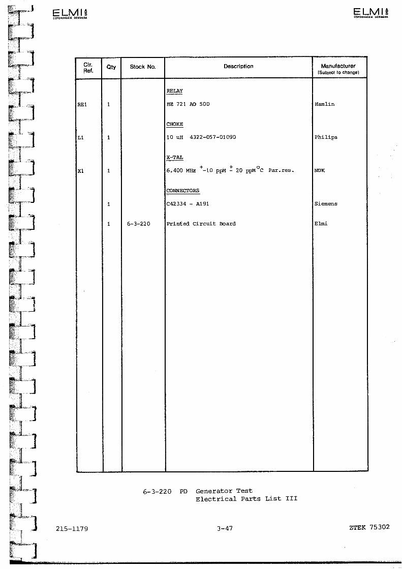
tTi
Li1[1Li
[1
Eji
L
ELMICOPENHAGEN OENUAHI(
ELMICOPENHAGEN DENMARK
RE1
Li
xl
Cif. Qty Stock No. Description ManufacturerRe (Subject to change)
1
1
1
I
1
RELAY
HE 721 AC) 500
CHOKE
10 uH 4322—057—01090
X-TAL
6.400 MHz ppM 20 ppM°C Par.res.
CONNECTORS
C42334 — A191
Printed Circuit Board
Hamun
Philips
NOK
Siemens
Ei.mi6—3—220
6-3-220 PD Generator Test
Electrical Parts List III
215—1179 3—47 ZTEK 75302

ELMH
U:
ZTEK 75302
6-3—220 PD Generator TestElectrical Parts Location
3—48
LU:U:VU:V
U:U:U:U:U:U:
216-1179 U:
/Ic;

U
—iri
*Idh
—III-
N
0-t
>o
I.,U
a.
CN
—m
,.,
0
—In
0-l
U
a
N2:
In+
cDv,
(N0Lfl
0
(N(N
(N-t
C’)
(NC
’)
(N(N
U.
UU
U
ri0
d0
q0
—3
0wI.
0a-
az
—IF
0)
0-IF0
aNO
1••
Fl
.4r1ia
t3
‘6E
,_
x---izi—
‘I)
>-J--
-J-SE1
(N.
I
0z
+ILD
-II0
-IFU,
0
-II-
>U,
I:>U
,+aa>U
)+
>U,
+aa
0
a
>In+
Fl
>.rL
...
‘9I—
iIx
__
0Li
lx
>-
iiiC
Lr
4>
>(D
WU
____
_____
______
U)
L_
In#S
:za
Fl
UW
-a4•4
IO
S
-1!_
—-
_____
So
JO
S
)—
L;:i
IU
m—
-—
fr—sL
rL1o
0.4
I•
—r-
::—
3
>F
lizc:
-;
?U
,U
W+
051-
OS
r—,
ca8W
N0tN
i;d
03
0-3
;—?
In
>;
£.
S)
a
In.f
N
Iiz
(Na
(N—
(N
0>
Incz:’.,J(N
?U
,>
_4x
Iz
+U
,t,
z;
LX
(%4
______
:D
.o
o—
=:I-ti”
I
0n
a
>z
H:2
I—U
,O
S0L
a.m
LD
::a
;
>,H
or
•.S
:
0
>-_t
ed
!.-,
C)
->
z__
L4
j.:?
-?.:i
jG1
ft
a:
IX-4
÷(%4
.+
C)
I\
+I
I
>>
::E:::\I
U)p.
U,0)
Q-3
sL
i.;
I1r
CN>
Lfl
Xr.’_lx3
.4.,_a
IDN
I—
40
U)?
OSOS
N
_________________
Olx
0)
>-
‘0
::
NI-
(NN
NW
In
0
o_e
WU
,al
Q_
‘_x
>0
(0-
T_=
4F
l‘o
-
-aa
‘—
NN
Fl444L
__
‘—.4
0x
Inp.
I
_
cz:cx
->
L1P
/L
j-
-X
ra
.;p.
InIn
IC
hD
QC
’)
I-N
:-
In
:
a.
I-
a-t
C(N
R0
0
C>
U)
aC
’)U
)0
o_2
o
)-0
—N
>,-
f!-
,>
+In
.-7
N
,-
ra
>‘-
0-‘
—a:
4+
—‘
t—..
Fl
NIn
In
I,‘—
k
0O
e>
Q:x
0a
1W-
10
lC
rlc
>i_.4
0
C’)0U
)
Er
3J
04J3J
Iiwo
0
OSp.
In
C
0(N7wIn::
-k----
OS
-;
N-
--aU
-
In
!-6-f.•i
(0(N0
(0043
0(N
00
--I_
0
I.
1—F-I(N
-—
—.r
——
—

1
ClC2 ,C7C3C5-6
C8—12C15—22C2 4
C13,14C23 ,25
IC1—21C31C4—51C6,11,1C121C7—9‘doIC1 31C14—151C16—181C19—201C2 11C221C23—24
INTEGRATED CIRCUITS
741S 293J741S 04J741S 08J
741S 379J
74LS 188J741S 157J74284J74IS 86J741S 283J74LS 273J741S 74J72 72 3MC 1408L8
Qty Stock No. Description ManufacturerRe. (Subject to change)
1
CR25CARBON FIlM RESISTORS type
2K2 2322—211—132221K2 1312212K 1312339K 133934K7 13472
METAL FIlM RESISTORS type MR25
RiR2R3R4R5
R6—10RuRi 2
P1—2
IC25—27
UUCCCC
1K47 2322—151—514723K01 530124K02 54022
1TENTIOMETER CERME
200R 3299W—1—201
RESISTORS NETWORKS
lOx 4310—101—103
CERAMIC CAPACITORS
11111
511
2
3
1212
14
4
212
3
311232112
22 nF100 pF22 pF33 pF
2222—629—03223° 638—10101
° 1022910339
Phi lips
Philips
Bourns
Bourns
Phi. lips
Siemens
Spraque
Texas
Mrtô rr 1
100 nF 837449—6104—S2
ELECTROLYTE CAPACITOR TANTAL
10 uP 20V, type 150D
6—3—221 PE Oscillator Part B
ElectriCal Parts List I
ZTEK 75302 3—52 218—1179

TRANSISTORS
2N2907A2N4303
CHOKE
10 liE 4322 —057—01090
X-TAL ++ 0
8.388608 MHz —lOppM, —2OppM C Par.res
CONNECTORS
C42334—A191—A701
14 pins C93—14—0216 pins C93—16—02
20 pins C93—20—02
6-3—221 PE Oscillator Part B
Electrical Parts List II
ELMIcoptuUkGCW DEMUARK
bL1ICOflUHAOKU O€MMA$*
Cir. Stock No. Description ManufacturerRe. (Subject to change)
TiT2
Li
11
1
1
19132
1
I
1
:3
IEu
Eu]:3
II]
]
Siemensmelco
Philips
Dantronik
SiemensTexas
II
Eimi6—2—221 Printed Circuit Board
219—1179 3—53 ZTEK 75302

t_J
LJ
L_
JL
_J
L_i
L_.3
t.—i
L_.s
L...a
LL
C_
aL
aL
_a
La
C—
sL
_&C
_a.L......a.
‘L
r—
—
__
__
__
__
__
__
__
-
03-iU0
m(n
1-i-
i
(11(13
I-4r4
0(1
1
e11
ri-I-i
-rIU
Uw
oz3
r’4
77a
U-,
(N00,
I-nN111
0,
Nf-if-i
a(N(N
(1
2

R3
C1+22n•0Vd
- (.0 .4 - 0C,., C’ C’ (‘ ,.j CN
12I 5 411615
45V V
D[L
71
__________________
6
IC12 7 [ 4 8
CL74 10LS379 15 ‘L.1 ovu
ii IOVd DVII
DVII
5J 61 211 al45V
I i4jiioiL_.f AD
1C9I 1 74S188 8
DO
916r2 1
7161! 4_zli 0
L-
10
9
65.53 Hz•
_114
1C3
1C31 14 76L508
oVd
D
2 1C4
6 13 12 7 ——
1C3IC4
U 10
C3
1C6:1c46
1C3:76Ls04
7 12
6 14
5 3
4 5
11
2
6
8
IC 15:74 LS86
•5Vo
131’
J..,C8
19 5 Vcc
16 6 4 DA
151o14 ..c10
+12 8 Vref—
1K47
0
____A
R6R7
6 10 1C23 1K67
5 1408L—2 12 camp16 0
VEE -C51 2 3 33p
200
QY1—15V
12 11
OVa
Cf2P2+15V
6 VcVc 0Vte
R12 Va1° U
6K02 1C22 6 RiO aoNON
1 NV.INV
‘ 72723 13C71K67 200
C 13 + 3K camp loop
10)1_V
a
P2 R811(47
D41
16Vref IS
A1C24 [iR9
1608L—8 1K67
camp 16
VEE C6iIt-::___-T 33P
I LC11 I1 L15V
OVa OSC1 OFF
4
1L
3
13
21
12 11 10
4SV
161
1 Internal Prom-ciddress Bus ( 6) —
AD
1C73 745188
DO
12111
U
•5V
6
3.5 43
1C3 14113
_F11
16x1ZI10KI
5110 I
765
11 5 2
+SVsI 161
C6
3
AD
1C8 I765 1S8 Li
DO
4]12 1OVd
6
b
S 617
17
A
16x
16
15
116
10
•SV
L
8x10K
IC26
B
ELMICOPEMUtCEN DENMAUK
IC1O76 L5157
V
97
P6
7556
53
42
31
205
12 9
16
sj
OVd
Internal Prom-dQta Bus (8)
11
7 6 54
1312 S1616
%LlHH
DII CVII
70 7
13 6
1 S
4 6
V
10 3
13 2
1 1
6 0
45V
OVU 10 20
617 1C19L_J6 76LS2736 13
3 8
2 7
1 6
0 3CK CLR
3
2
a
IC 14:741.585
b2 2’
I 1C27 L15VL 4x10K10 1
7J______12
+5 V
161
2
IC 1374284
A
IC 17
76 LS 283B
Co
C6
A
IC 18
76LS28B
CO
1DVII
12
14
3
5
11
15
2
6
6
0
LI)D
C
EDU)
a)VVa
aC
a)4-
C
+ 5V
))L6 CO
A
C4
OVd ____1.068.576 Hz
8 4 5
A
DVIIRi5V
T1‘2N 2907A
+5Vo—
131’C1O
VecOp1I
DVII6
A
IC274 LS 293
cc
,SV
20
IC2O741.5273
3 80 Q
1 6
19 S
16 6
19 7
12 8
0 9
5 10
5 11
O 12
c12
‘5V
L110iH
+SV?
R54 KY
CK CLR
,ic\
11J
_______________________________________
12
C2FG42N43O3
:i3RB
xR45
T2 I
ADJUST
22p111 39Kj IC3 ‘
OVd I
___________________
OVU X : 8.388 .508 Hz
•SV
JcLJ!1
IC676LS379
0
2
7
ID
74 LS 08+5V
4
51C56
112
OVU
-pp
p
p
15
_____
OSC2OFF
— - — +l5Vo .15V o30
F Q3 C23 C22— - 1- - I
ND obc28
I I C25 C26I 1 ?‘ _I_ p T T -15V obc32
I 1IJ IOI11 OVa -15V1 111r Ct37 P I 5V
—I 2C
C2 11CK,
C2iC2Cici8I 1L16i C1L C161;0abc 2
2D 10i4 T I I I I I T 1 obc6
c_j 121 21 I I 01 D.GND
ZI L.J I OVd
cI LI)[
L:
Iii.1. OVdOVd
m
là c- .3 0 a,cb
3 ‘3C
6-3-221 PE Oscillator Part B
Circuit Diagram
221—11793—55 ZTEK 75302

COPENHAGEN DENU000COPENHAGEN DENMARk
Cir. Oty Stock No. Description ManufacturerRe (Subject to change)
CARBON FILM RESISTOR type CR25 0,33W
Ri 1 11(5 2322—211—13152 Philips
RESISTOR NWORKS
1C25 1 220K 4310—101—224 Bourns
1C26 1 lOX 103
1C27,28 2 11(5 152
CAPACITOR ELER0LYTE TANAL
Cl 1 10 uF 20V type 1500 Sprague
CAPACITORS CERAMIC
C2—7 6 100 nF 9/0145 — A Ferroperm
INTEGRATED CIRCUITS
ICI—14 14 CD 4076 BF RCA
IC15—18 4 74 IS 283 Texas
IC19—22 4 74 IS 86 J
IC23,24 2 74 IS 157
CONNECTORS
1 C 42334—A191—701 Siemens
20 16 pins type C93—16—02 Texas
4 14 pins “ 14—02
1 6-2-222 Printed Circuit Board Elmi
6—2—222 PF Oscillator Part AElectrical Parts List
225—1179 3—57 ZTEK 75302

N Di
Li
w 0
to to to
NO
Htf
l‘D
o0
H
H-D
J
0r1
‘-ti
tD
iD)
rtrt
w 0 0 Di 0 0
U)
-—-z_
L‘
‘
_‘
I,
bt
TI
‘I,_
4I
ai
i—aii
i,i
II_‘.J
si;
‘i
at
ii
(II
ai
114
1t
iJb
gj.
—aL
ia
VI
II
I4
II
‘I
I41
—I
4I
II
II
1If
I•
aia
i’,
iIIII
a_—
I
iit.a
a4a
I4l
II
:a
i4
1-
‘3
k‘
‘‘
‘‘Is
‘‘
_____
-w—
-r’
-——
.
‘—-
—-
‘4
-—
I;.%
41K
fj
II
tt..
tat
—F
it
II
tI-
,I
I_I
._t
;
__
E
__
)__
__
—I
i1I
i4,1
r—
(I
U
\4(I
-
IIII
_(.J
(I.;
4i—
I_
IIi
•1I?Ir
aT
,—1
4tr
tI,
—--
—-L
_‘J!
’:
-!--
ç0
-
4,---,
4.
,:_‘4:-.i4ti
i,I
IIJI
i__t
t4i
i1
iia
1s
ji-4a
1_
_+
g,
-
•I-
)P4-
It14a
i)(t.
-i’4r
tit
ft
iiItifg
4
I.
‘4 14
cni>
-—
fl-i
-Ii
__:
q_
1
——
——
a

a6ci8
alOa12all.a16a18a 20
0
2
456
7
1C258 x 220 Ks -
- jio+5V
-J
0
23
8910
11
4 6
5 2
6 15
7 11
5
3
1612
8 6
9 2
10 15
11 11
5
316
12
IC 278 x 1K5
i116LS86
)8 13
- ZDmK5-
1C20 8
jiosv — -
-
Jio5V
!_
6—2—222 PF Oscillator Part A
Circuit Diagram
ELMICOPENHAGEN GENUARO
[?.IC26I4* iox [-io5V
61 5 6 3j
OSC1IØ I ICISC 210nscl Il
cl 2 QSC 211
10 S S 5.4-
6
3
I
1657 6
I_IVI ICOPENHAGEN OENUflK
2 Il
.J_.1 1012199171616131
I 15j1413j12[11f10j 91810 6
2 15
3 11
53
14
12
1C258x1K5
5V
Data Bus (8)
____________ ____________ ____________
llU13Ut 11U1?
il_Fin1::11 ii
ni54_1_4615141_3 2 1 0 — 2 1 0
1112 13 1 1112 13 16 11 121131161 111121131 hI
_____________
L L!J D 16
CLD 16
IC2 1C3 tC LIC6 5v
____‘sD
9”100D IC1
______________ ______________ ______________
08 Q Qa
3IL1_
6076
oDfr2p
6076 6076 00 R6076
00I_R6076 4076 orL2
6 5 6 36563 6563 6 51413j 6j5I4I3
6j5f6j 7J6j5[6i1j [8] 71
A-Bus (12)
_____
—
9 1 1 91 61 21 971 61 Sf 431211101
IC 1574 C5283
A
C4
9
7
Co
B 1C1676 LS 283
A
17
116
151S
OSC1 OSC2
65536 Hz
Y21C26 Jiosv4* 10K j
9 10 7 B
On
B
Sv
4
7
6 0
1 1
13 2
10 3LI
4 4
1 5
13 6
10 7
LI
1v5v6 8
1 9
13 10
10 11
LI
4
5
6
7
I C 23761.5 157
Y9
12
00
I
A
c15
c20c18
b 20
a22
C69
7Co
B IC 1774LS283
A
Yo
Yl
IC 2474 15 15 7
1Cl.
9
7Co
+5
a24
Lb2L
Y_ c26Y
9
12 6
13 2
_________
ll.lSBIcjS
03j —
________________ _______________
—
_________________ ______________
—
_________________ ______________
iL_jl 741.5283
.
-: i: : : : r :_
_
Lz__ -—- —- Internalodder B—Bustl6) Cl.9’
-
----
InternaL adder Sum-Bus (16)
A12
!o5V4 12
1 13
13 14
10 15
LI
I I I I I
Ti
5 V +sV
I i. I ICT c1 cr q-
OVd
_.I__ I
0)J1 TP RGNU
/__ _•\
1 1 •b o5V
I Ri] PF
227—1179
3—59 ZTEK 75302

3=7
024
07
Ci2’1 4
z01
I221
PZMTR NWOZX
1X 4310—101=103
AAMC APAC!TO
74 24774 373I7474r4 24074z.a 244747k 13fl774 i0774! 02
ONNOY4
C424—A1i1—0140 pine =40—02000 i A4KM
Printo Ciuit boa
P CPU Unit1ctric1 Prt List
i’I’g
Cannon
—
CIi Oty Stock No Qnorlptian MRnufacturetH.L tRubj.ct to chinp)
—
Ct0N P7i4 033W
IX 23222i1—i3102lOX 1310322K 13223100k 13101
Z0i7
22 p100 p100 flY
2222—G3—1O2210101
37444104—2
I1
]]]
]21IIIII
10 uY, 20’?, typo 10
Phi 1ip
ft
Phip
iemn
prqu@
ft
ft
N 0
I
II
1
I3I1II33I1
I
141
I
XI
X=ThL
Mt1 ± 0ppfli ±lOOppm 0
ZTEK 75302

____
— I
L
H
L[
• E
6-3—223 PG CPU UnitElectrical Parts Location
ZTEK 75302 3—62 229—1179
SEMENS

I ELMICOPENHIGEN DENUARK
6-3—223 PG CPU Unit
Circuit Diagram
HtI SUU MULL) IUIN
(.0c..J u.0 ci
100 z
4764
TRAPINTR.
INTTIM RST 75
R5T65I 9RST5S
flR622K
I 2:L3T6
KtAUY K2 xl
c3c6
5.165 MHZ
____
xl Cl
391 51 I 21
1UKHDFyI[1
21 11t22 8
23 13
26 6
A 25 15
26 6
27 17
1r28 2
a,
I II III
45678g1011121315
NC: 1129,33,3438
‘Cl 8085
Address Bus (16)
AD
15
5V
J12r1C9 L_J
14 11
A Y 12
16 13
74LS266 3 16
18 15
jij
+sv
95V161
22
15
16
5
1410 1
11 212 3
IC 13AB
C
RESETOUT
7 CLX WR ALE
371 3 311321301
+5Vr]JJJ,
119 F-i74LS365 9i
+5VL V9
13
QSC1If1J
0 1
1 22 3
6
5
A
B 1C12C
V
74LS13862
9
12
8 7
16 OSC11113 05C210
ncrii
6
17
74LS13662
12
_________
11
___________
10
9
7
GENIN
7
b8I blO
Ib1201
hblh3
A6A
__
- DIR76 LS245
ia MEASW/9 NEASLO/T
MEASHI
11 12
a
13J16[fSfl6 17 18
213145 6
22C62
6 374L5373 2 6
7 18 19 1CC 6jil
ACE
3 14 2
5 3
cD©
Li
©
13
IC1%
61
R2
_________________
U lox5V
1(SV
2 1C16:76LS02 15
—i•i;;_i sr•—_ C -
J’IC16)o -
I 5V
— R1+5v -J-. -RD 1K
‘ 76Lz,iioS 62
51
2 PR 61J B
6CKIC156
10KCLRQ ÷5V
f5V
8 1C15:IC 74L5109 ib 12 ALE16 13
1C16
98 7
AlT 1
-1
Y
76 AI[2
13 IECADR12 TEtBU1110 FfENAS97
-4
U
I-z
0123
12 73 16 15
‘IINT
1jBB
C 13a 14ciC 13clL
c15c16C 17
WR CLK
6J 5
181176 7
1819 3
5V
C6’C C4’ C3+1C2
T:T T T T1
P, kP
DB
9 11 10
i Oi1
—E :::: ALE
RD RD
w
— — — —
RESET — — — —RESET
t— — — — —
CLX — — — —CLK
21
1C2
CLX RESETWR RD C/D C
22
01 1
12111
k-f
Doto Bus (B)
r 2
I1 15
6
16
D.GND
A13
A:
ST 6J 1f171 19!
a RS
3
I
11
3’IC 8
6
IC8\J
161
BDJ C
I NIIC 3
10 21
PB CCX RESET WR RD C/D
+5V
22
a
12
b 15c7c8cliC 10c9
13
2
16
0 B:
3
15
6
16Lu
-
I—,
8279 SHIFTI36
CN TC1
RI _ 3 C
_____
O_i 39 1 2 5 7 8 31130129128 27
aol l7I 6J15 6+SvQ I I I
ii
.ta3 16 5 16 12
(‘.1 LflcDOU)_i
lmla,ImlI.rkrII
6J 7{
181191
a
17
c.1 I’7
3
I_ A 0R53 RI
32 33 36 35
9 11 22IC
5V
60121
25 24
8 11A
ICl0 74L5244
V
- ------ - • --------_r-_,•-_rw-_. - - -
; —I’.) C’.) C’) C) 4 U LO t- a 0) 3 - I’3 ‘
C”lC’3 CJr.4I’1r.J r’ .j (N (N
.0 ci.0uci.0u _0_Dciu ciciciciocicici 0000DD
--08 CCX RETWR RD C/C CS
4 NT
8279 ® SHIFT36 1C6 8279 ® SKIFT
CNTLCNTL
0B
UA RS
0RI
23
381391 11 2j 5J I I I 33b292827262526I 32I33Z 11 2j I I I 81
+5Vl I I I 5V20Ij7 6 15 6 73 8 ‘l 8 jj 20
16 6 3 i 1IA 1
ICS CS IC11 76LS264 1C8
76LS260. - 76L5260 IS
—
16 31 516 I 18f12l9,780 l-1
8loK
1C77
(N
9 0
B I
7 2S 3
S 64 5
3 6
2 7
a D1 012 D23 036 06
6067 07
05o6‘07o809
, olOoilC 12
C-
.0
V
_____________
C-a,0)Q)cQ ——rN(N
PG
230—1179
3—63 ZTEK 75302

- J
ii
I
HHI]
I
Cit. Qty Stock No. Description ManufacturerRef. tSubject to change)
ELMICOPENHAGEN OENI*AR$
Ri
Cl
C2-9
‘Cl—s1C9Iclo—il
CARBON FILM RESISTOR type CR 25 5%
10 K 2322—211—13103
CAPACITOR ELECTROLYTE TANTAL
1
1
8
712
118
1
lOuf, 20v, type 1500
CAPACITORS CERAMIC
lOOnF, 16V, 9/0145—A
INTEGRATED CIRCUITS
271674 IS 138 J2114 L
CONNECTORS
C 42334—A191—A702GO8D 16A4 BEAR24 pins C93—24—02
Printed Circuit Board
Phi lips
Spraque
Ferropexm
IntelTexasIntel
SiemensCannonTexas
Elmi6—2—224
222—1179
6-3-224 PH Memory
Electrical Parts List
3—65 ZTEX 75302

tiL.
EL
Fr
L
ELMIj;jJ
ZTEK 75302
6-3-224 PH MemoryElectrical Parts Location
3—66223—1179

A1C7
2716
Lo 9HJIII
it,
5V
eC’1
I I I
lU[lll31ltel1lDl91l1 I1
+5V
liZc6 c8 dO c12 c16 c16 c18 c20
a6 8 dO o12 a14 a16 a18 e20
A1C5
2716
nl 9J lull lJjlL4lQ ID Id
0 1 2 7
6—3—224 PH MemoryCircuit Diagram
.h1JJ
Li
Lfl
4 I= I
—‘
o 1 236 5A
A
717T6 7 8 11 121 19 10 15
ELMUCOPENHAGEN DENMARK
c32
O147910 o1123J567J8I91c O6567181 0112316156178191
zIL3l 876 [2i]23 9 8l7 632 3j2I 8I765L3213l1 7j32117h6l1_+5V+5V 5676I312111716l15I
A —120 to A —120 [ A Z120 0 A —1200 A 0 A
IC1 2716 1- 2716 L 1C32716
IC% 2716CS1— IC1O
2114 L I IC 112114 L
o 0 Vpp 12 o 0 Vpp 12o Q Vpp 12
oVpp 12
1 6 CS WE 1 6 CS WE0r PDLPoy i,o 110
1 it11j4 l[l 21, 26,1 9917+ [T1 21 26 ( 12,fIJfl72lI, 26j,
U5jTT1 12+ i! 16117 2lJ 24J L t •• 10 1613 121111 8 10
.21[L3j 5j7 ÷5V- oi2jz +5V iJ234567 +5V +5V 656171
LI_________ -
DOtQ Bus (8)
151613
RD
Ri+5 V
10K
4-
3
111213
1211lu
5v
116
61 0‘cg
76 LS138
ASC
62
48j
15
97
I A
‘1
D
RD
U
8 7
2
6
3
5
6
6
5
3
57
21
U11 2 3 4 5 611 1iu
6 5 6 3 211 2319
10 A 10
I 1C8CS
2716 PD 18
10 0 Vpp 12
]011 13161511617 2lj126,
oh 2 3 6 516 7 5V
Address Bus (16)
PD[1IVpp
LI
— d30
+5V
01 2
876
o 1 2 3 4 5 5 716191198765632 I1IigI
O A 10
1C6CS
716 PD
O 0 7 Vpp.; 77 P+.l -
3
5
4
6
9
0
5
3
la.
6
2
18
1
+ 5V
I
D
PDL1
Vpp
4J+ 5V
3D 01 2 7
ad 2
ac4
jjjj1 +1
Cl 10?C C8 CT C61 C5T C61 C3T C2T I ov
Op 1 D.GND
PH
224—11793—67 ZTEK 75302

k1JJ
Ri ,3,5
R7 -9RiOR11—12
Ri 4—29
R2 ,4,6
IC1 6,18
19,21,
22,24,
25,27
1C17,20
2 3,26
IC1, 41C21C3,51C61C71C8—15
CAPACITORS CERAMIC
100 pF 2222—638—10101
100 nF B37449—6104—S2
INTEGRATED CIRCUITS
MC 14532 BCL
CD 4071 SF
74 C 157 J
CD 4023 SF
D8155
114 339 J
Motorola
RCAN.S.RCAIntel
N.S.
Texas
Phi lips
L
Er
[F
El
6-2-225 PJ Receiver Test Input
Electrical Parts List I
ZTEK 75302 3—70 231-1179 [
Qty Stock No. Description Manufactuter
e(Sub)ect to change)
CARBDN FILM RESISTORS type CR25 0.33W
22K220K
1 OOR
2322—211—132231322413101
4K7 13472
?PC RESISTORS
IRS 2322—660—93001
METAL FILM RESISTORS type MR25
R13R3 0R3 1
1K 2322—151—21002
953R 29531
909R 29091
RESISTOR N7TWORXS
47K 4308—102—473
lOOK 4306—101—104
Phi lips
Philips
Philips
Bourns
Philips
Siemens
Spraqua
331
18
3
111
8
4
13
1
212118
14
16
‘4,5ClC2
C3
CAPACITOR ELECTROLYTE TANTAL
10 uF/20V 150D
IEII
CCCr
31—14
1—16
DIODES SILICIUM
1N4448
DIODES ZENER
BZX 7915 C

ELMICOPENHAGEn OENUAME
COPENHAGEN NENUARN
Qty Stock No. Description Manufacturer
e(Subject to change)
C0NNEC0RS
1 C42334—A191—A502 Siemens
1 40 pins C93—40—02 Texas
1 6—2—225 Printed Circuit Board Elmi
6-2-225 PJ Receiver Test Input
Electrical Component List II
240—1.T793—71 ZTEK 75302

ELMU ELMU
U
6-2-225 PJ Receiver Test InputElectrical Parts Location
L
H’
I
1/ttT’
I lilt‘°UflWWflWS1JWVW di
SIEMENS
232—1179 3—72 ZTEK 75302
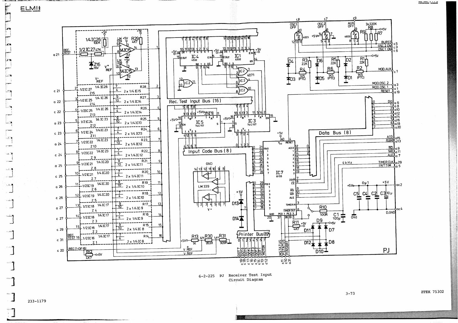
COPENHAGEN 000USfl
a
c 26
a 27
II
c 31
I
1 233—1179
R26_— 2x1/41C14
R25_— 2 x 1/41C13
_Z_ R24—s-— 2x1/41C13
R23_2x1/61C12
R22_— 2x1/41C12
__R21
.JP_ 2 x l/41C11
R 202x 1141C11 —
1 222 233 264 255266 277 28
R322K
R411<5
(PTC)
12 013 114 21516171819
78
MOD. OSC. 2MODOSC 1
REC.TEST 1
2
b
2
7
3
c8
17
.1
I
I
osciOFF
7TTflT5 9 111?41316T15
10111213j
j 5V l0h113 1 2 +5V1234k
ENo_Lb0 IC1jI4
s+1+6532 sI 6532 ]14
Q 1 2 1 2
c7
13
9
12
SC2 AUX’ 3x220KOFF OFF1
E‘10
6023 +5Vo J-i 6023
R9 11-1R7
11) 8 ii Y RURST
-1/21C271/61C26 R28..
Z15 -
-- 2x 1/Lids
l,2IC2511426- 2x1/6IC1L
114 9
a21
c 21
a 22
c 22
a 23
c 23
a 24
c 24
a 25
c 25
I I 0SC20N
I
I -
4
A
I
_t_
c3
D3
51 bI I1 b
Rec.Test Input Bus (16)
D6
31 31 EilOl +SVo2tl4sI h1
2
3
6
5
6
7
8
9
10
11
12
13
LAUX
11<5D1 {PTC)a
1
10
EN
J_ 1 i
6
36 113 76 3
76C 157IC 5 ___JLf
12 7 9
3 2h
IC 376 C 157
3
1/21C25 1/61C26
I..
1/2 IC 241/6 IC 23
C1/21C24 1/41C23
1/21C22 1/41C23
z_i.0
1/21C22 1/41C23
9 1/21C21 1/61C20
Z8
_______
1/41C20
Z7
26 1/21C19 1/61C20
12 [1,21C191/41C20
C z_5
131 1/21dB 1/41C17
L161 7/21dB
1/41C17
L15j ii2ici6h1’4C17
16 11I2IC16uuti7
Z1
S
76
Cl
03al019
a6a8dOa12al 4al 6olOa20
Input Code Bus (8)
+ 5V
1400
4
GND
0 DO1 1
2 23 345 56 67 7
A73Data Bus (8)
R192x1/41C10 —
R:
9 R172x1/41C9 —
RESET
PAD ADO1 1
2 23 34 65 56 67 1C7
9155
I0/MCE
RAM •2
-n
4kHz
WR nilAl F
+ 5V
D13Av+
O 2I 3(2 33 14 3i5 3’6373t
-f R16 142x 1/41C9 I
- 1_a. R15 I 152x1/41C8
—:1-— R14 16
EELIC-
07
2QTIMER CLK
REC C1-OF-16)
9
INTTIM
PB 0I236
S67
GND
RD
WR
ACE
in
7
11
• r41_
LO+5V4K7
D16::
O,jl - +5V
TIMER OUTPCO 1 PC2 3
20j
oc 2
37
C5C4j C3O pS
fnter Bus
p_IRh4K7 Dli
,R31I ii 2
01010-
01010
100R C ‘
D9 lOOpI——-°5V
I :D7
3{ 4
B
J
•57
lxIN—C
o090:
(JDI.
U)
Dl 2
?!22••.:cP)U U U U 00 U )J
L
010w
: D8
uu a
6-2—225 PJ Receiver Test Input
Circuit Diagram
1___1_____— ,0C4
_LOvu
P]
3—73 ZTEK 75302
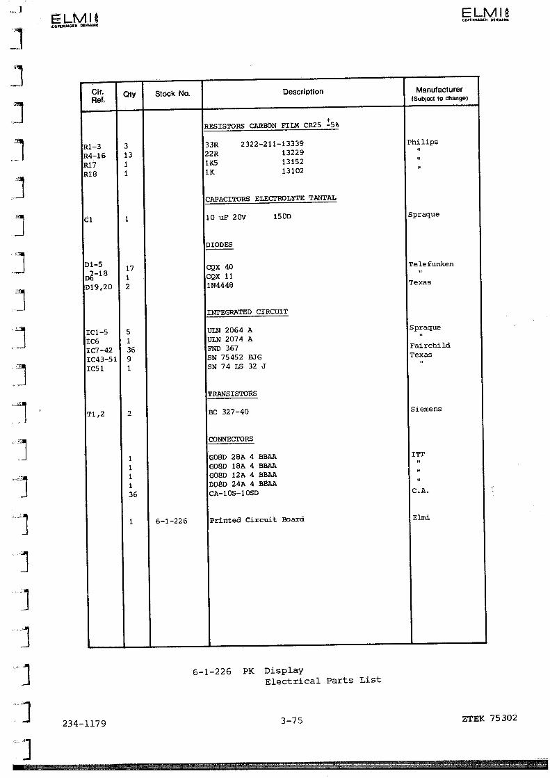
ELMICOPENHAG DMAHP
ELMICOPENHAGEN DENMAHE
234—1179
111136
INTEGRATED CIRCUIT
ULN 2064 A
UW 2074 AFND 367SN 75452 BJG
SN 74 IS 32 J
ONNECORS
G08D 28A 4 BBAA
GOBD 1BA 4 3BAA
GO8D 12A 4 BBAA
D08D 24A 4 BBAA
CA—lOS—i OSD
Printed Circuit Board
6—1—226 PK DisplayEleCtrical Parts List
ZTEK 75302
Cit. Oty Stock No. Description ManufacturerRef. (Subject to change)
RESISTORS CARBON FIU’4 CR25
33R 2322—211—13339
22R 13229
11(5 13152
ix 13102
CAPACITORS ELECTROLYTE TANTAL
150D
R1-3R4—i6R17RiB
Cl
D1-5
D19,20
IC1—51C6IC7—421C43—5 11C51
Ti ,2
10 uF 20V
DIODES
cQX 40CQX ii1N4448
31311
1
1712
513691
2
Phi lips
Spraque
Tele funken
Texas
Spraque
FairchildTexas
Siemens
ITT
C.A.
Elmi
TRANSISTORS
BC 327—40
1 6—i—226
IIIIII
3—75
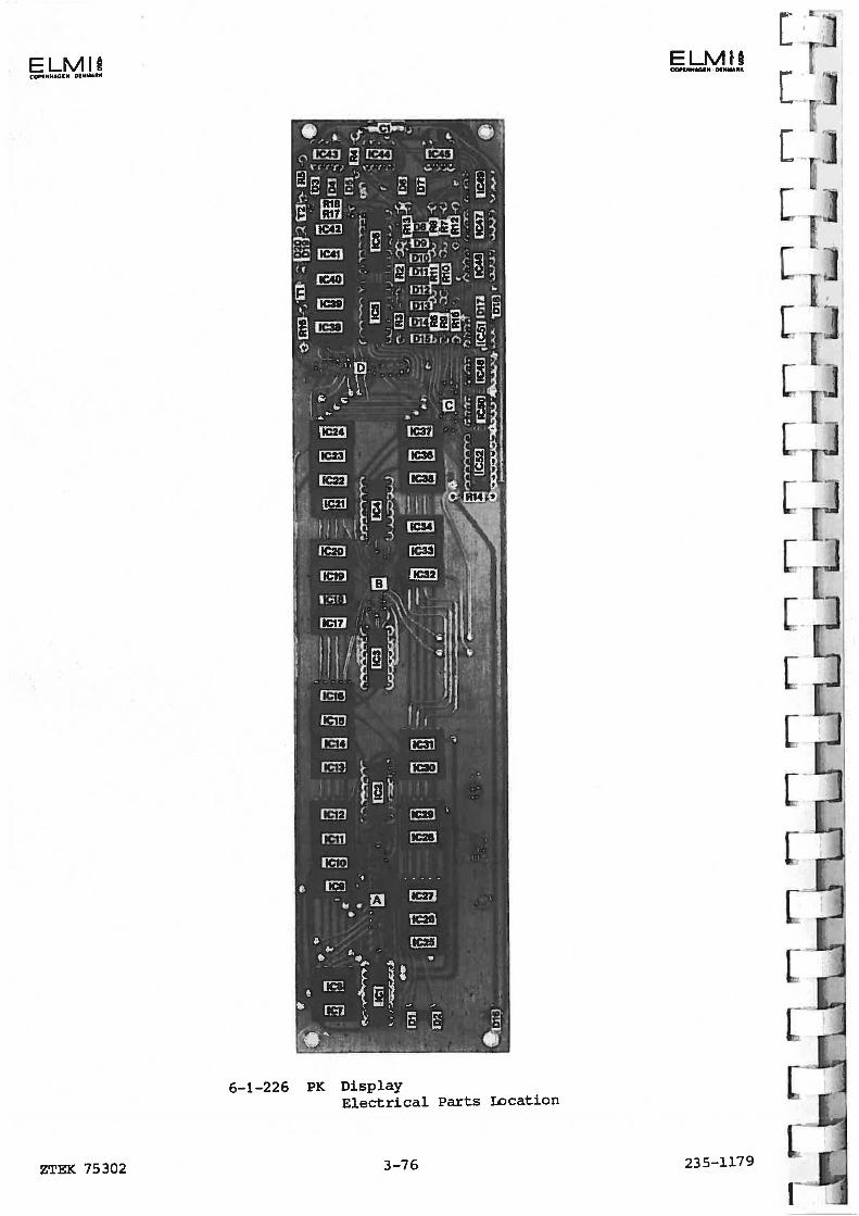
L
LJL[1[LI
[[LI
[IJI
[JI: HV[5V
F
PE OEM MAR K
ZTEK 75302
ELMUCOPOMNAMEM DENMARK
235—1179
6—1—226 PlC DisplayElectrical Parts Location
3—76

ELMICOPENHAGEN OENMARN
bLIVIjCOPENHAGEN OENUAEH
‘(A 6I(A9‘(MO‘(All
segm€
ab
Ue
Decimal PointsC
7—segmentdisplay
Ii 12 16 17KA
1C23 1C21.
-1I
088
R6
1(1.6
b fc 5V.
R16 2211
BC321-66
019 6(337-40TI
D20 T2
R1711(5
R18 —1K
1
2
3
L
5
FND 367
commoncathode
f 1
9 C
e OF.
,.i commonCOIhOS
lC7— 1C62
10
9
8
7
6
DecimaL Points
A t2
12
‘((4 ‘((2 PEril ‘(CS ‘((8 ‘((7 ‘((6 ‘((9
AllII
.5v
1L
(52
121C52
76L532
A,B—UAIAé#2-A3
RL-R15 7211
03-018 COO .6OlEedl
CIX —11 (greEn)
__________ ________ ____________ _____________ _____________
RAE.
KA23‘(A??‘(021‘(020
KA25‘(AZL
A2 Al AO 63 82 61 60
06 05 Rt{I
_______ _______
D6
______
— d8u mS 0CC 6(1
_____53S
1(0 IC1O (Cli 1C12 1C13 ((16 lC15 (016 (Ci? (16 lOIS 1(20 1(21 ((22
[111 I T I I I I I I
F5
______________
segment B
a ((.7 1(6
__ _
___]1_
L
_______ ______
segment bus B (7)
_________ ___________________
__
H
HMA
___
________
segment bus A (7)
1C43— IC 51:75652
SVX_!I 75452‘(C 3‘((10
4
REt. COMB.
segment —bus R (7)
tN NO.‘(C 12
‘(C 1
‘(06‘(0 5‘((6‘(07‘(061(02‘(03
‘(A 5‘(08
*1HHH
L9
L]
L]
01 ST01 02
ABS. REL
C EVE L
CO X—6O
1C25
Op
R 11 11 11 R
((36 ((39 ((40 IC 61 1(62
1(27
ILl12
segmentRa
b
d0
0
1C28 IC 29
Pu
1(0211(020
1(0191(016
‘(Di?1(0231(022
PA
lC3iIC 30f 1C32 1(34
‘(AL1(65
‘(81
KB S
‘(810‘(816
‘(86
((35t IC 36 IC 37
—. NC
9 2 t iF —-fl} ‘F flj 7r;-1-——— 2 7 16 9
112,13 11213 11213 12,13
2066 6.5 2066 ‘.5 I 2066 4.6 6.5 2066
(Cl 1(2 I (3 1(6
14 ii 3 6 3 6 16 II 3 16 6 11 3 6 14 Ii
SCAN , # 1 - Of 11 21j f 6J6Ij f 6Jjlj 1L3!16 IS
27 16 2‘(A
RD 1‘(026,SVA
+.:L Ci10 p
‘(Al‘(A 28
cathode drivers
KAi4 i 16 17 B 7 11 12
‘(AlS KB KB
,
9 7 2 1
tif‘Si1e:
2076I ItSl:i::1 CO
1IZJ 11 6 3 16
5CAN,2—0 I 2 3 1. 5 6
16 16 15 13 10 9KU 1(0
R1
.:!I3 x 33 11
Ii
6—1—226 PlC DisplayCircuit Diagram
12
PK
236—1179
3—77 ZTEK 75302

IC1—161C17,181C191C20—2225,29-3)1C231C241C26 ,31,321C27rr2P
INTEGRATED CIRCUITS
SN 7552 BJGSN 741S 32JSN 74LS 138J
CD 4099 BF
CD 4071 BFCD 4556 BF
9374 DC
6-2-227 PL Keyboard
Electrical Parts List I
CFairchild
Texas
239—1179
Qty Stock No. Description Manufacturere. (Subject to change)
CARBON FILM RESISTORS CR25
1 BR47R22R27R15K56K47 OR68K1KS
2322—211—131891347913229132791315313563134711368313152
MJJ
R1—38R3942,43R40,444R41, 47-4R45557R5 0R5 1 ,52x53R5 4
1C33—35IC361C371C38
ClC2
C12
C3—11
01-708,9010D1 1—43
RESISTOR NETWORKS
1KS1K53K33K3
type 4308R—1O1—152431OR— 10 1—1524306R—1O1—3324308R—1O1—332
CAPACITORS PLASTIC
10 nF 53256O—B31O3—322 nF B3223—3
CAPACITORS CERAMIC
3834331211
3111
11
1
9
72133
1621
6
11
3
11
tI
El
[r[LI
c100 nF B37449—A6104—S2
CAPACITORS ELECI’ROLi’rE TA1PAL
Phi lips
H
Bourns
Siemens
Siemens
Spraque
SescosemTexasTe lefunkenSiemens
Texas
RA
10 uP/20V 150D
DIODES
SFD 129 B1N4448CQX4OCQX1 311
germaniumsilizium
SN 741S 123JIE 555 JG
ZTEK 75302 3—80

TR1NSISTORS
BC 327—40BC 337—40
KEYS
RL 1 TRLP 1 T
EJ
T1—21T22—31
M—33A34
ELMICOPENHAGEN DENUARK
Qty Stock No. Description Manufacturere.(Subject to change)
2110
331
41111
4
1
Siemens
Sadar
nor
U
R.S.
Elmj
QJNNECTORS
GO8AO8A4BBAAUBS 4A02 8C4DLUBS4AO 1 BC4DLUBS4AOI2C4DLUBS4AO24C4DL
Power Connector 128—254
Printed Circuit Board6—1—227
31
Ii
ii
1
I,
I] 238—1179
6-2-227 PL Keyboard
Electrical Parts List II
3—81 ZTEK 75302

__
k%T1L’jj•.fa —
6-2-227 PL KeyboardElectrical Parts Location
ELMU
CCccrIT
ITLI!
IT[VVV
V
-i$
237—1179 I
COWflMAR
ZTEK 75302 3—82

02 03 0 05
A2 A3d A4d ASd
ST*V
.L. #
*11-13*
X3fl-4*
IV *43L7*
C 111—1.1*5 p4*—rn
*14- 214
44%
—Is—a—n
—1—a
LV 4—s—s—a—3
J ELMIVOP%NVAGEU DENUA K
I
I
I
11%15
llIIII IIIIII
-n3*3
‘‘ 111T1 llTflfl *7
________
U’,
_________ __________________
C S I 5V3
.49
cs—ce ,E
IC4093
.5*
___________
n]
L*A2 WDKA7 *2
nil1._i *5*4.19 I IV*p .LTI I 1C32
9314 93141C37
rn—A) [ 9 Al—Al
_______________ _______________
4 343
ITT I
_______
• 4111A
tl
__________________
LFU 11 3L ‘
IFS J
SCAI (02*14* *1 I
________________________________________
COXLO CQX13U
COPENVACCU *1*439;
9IT1t7
I-lw.55 .55
_
NUll 4704 .5K
4 %PESEC
iti hf Jill I
V .1.C2 A,B-I2ATA,#2
1615121
C
-It
64*
LIII
t.
.41 L
1
2*
15*
3IC% 18.1*3
543111
I 111C261 •Il -
*4 4 SAl
L53—i q—II I Jss* I I
01*
.64
‘II
‘14]
__1I4C25IlI;-
L9L.55
CIII
T 154J 121 II)
II H
1,2 1C383 • 3*1
1 ‘I
(.1
srt41058
/
‘ t ——‘——— —
AS A A? / AS . A101 Alit
F*CS tIU
-IV
P52 -5
470*
1153IS
T
IRIS
1C26
14*(2514
C3I
I12p 110n
1 Hz
____________________
‘IV
.5K1 I 5
4*1* *2 Al Al %W8
1C20*099
L
Ai2 A13 A16
I411*,_ :;•— *4t,2
863
CUP
-15’
A15Von I
At? Ai8 A19
/ -
I I A21A
tsr IA25 2& A??
LIII
A79 A30 A31
•VS”__
5521- 1C224093 5
d
A
A20
A26
A28
A32/
(23
4416—IS
.59
6011
..50
CQ* 1350 012—1363
18* 1122-1135
76 L532
KEY *tTVIN LIVIS
*2 A.I (AlA, 33
IFS 40.
*0
2E1 rat
255 TESS VOLT
_
832
—11 87
—II
—12
—, *50
851
gA
34*5 (00818*, 0 3
444 —80844
I3LIJ
__ _
OP IEtI
60*0
4,99*5*•pl
6-2-227 PL Keyboard
Circuit Diagram
241—1179
3—83 ZTEK 75302
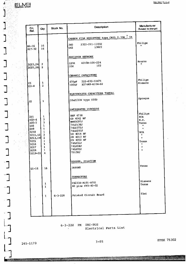
EJJ
Cfr Oty Stack No. DescriPtion Manufacturer
Ref.(Subject to change)
CA ON FIU1 RESISTORS type E
R1—16 16 31(0 2322—211—13302 philips
R17—32 16 61(2 13622
RESISTOR NEIWORK
1C23,24 2 220K 4310R101—224 Bourns
1C25,26 2 10K 103
CERP,NIC CAPACITORS
ci I 470pF 222—630—03471Philips
c3—4 2 lOOnF B37449—G1O4S2Siemens
ELECPROLYTE CAPACITORS T1IAL
C2 1 lOuF/20V type 1501) Spraque
IW]EGRATED CIRCUITS
id 1 BE? 4738Philips
IC2—4 3 CD 4042 B?RCA
IC5—7 3 MM8OC97JN.S.
IC8 1 74LS138JTexas
1C9 1 74IS375J
IC1O 1 74LS293J
Idil,12 2 CD 4014 B?RCA
1C13,14 2 CD 4013 B?
IC1S 1 CD 4050 5? “
IC16 1 74IS32JTexas
1C17 1 74LS04J
1dB 1 74ISOOJ
IC19—22 4 75138J
DIODES, SILICIUM
p1—16 16 1N4448Texas
CONNECTORS
1 C42334—A191A7O1Siemens
1 40 pins C93—40—O2Texas
1 6-3-228 Printed Circuit Board Elini
]
6—3—228 PM IEC—BUS
Electrical Parts List
245—11793—85 ZTEK 75302

6LIIEt7OE9L)IalZ
UOTDDOSDIDTDeI
Sfl-DINd8-E-9
91/61SN3ri3IS
____
‘I4
LIJo4
4
,0
••4ee._.
-----
---
4
__
-._.4.w____-____--;Th
0-
a
•—
•0•o_
-
-tEl-
---:•-———
-0---
-:iii--
———_———._I(——a
____
-
a
••
—————
UEJ•IEI
:..‘.—-i::.;-I.
20-0-•a
4•e--.
Dl!!-
-
•————-0-IJJ.
t-f.1j__:i___4-;‘j-rI:j—
a
IJa
0-•4-
4
I—__—øi.—m—.a
•0-rtI5L)--
—
----
•
--•
,.;::: D1—”0-
--I,iYi’I‘.i-(r‘
-[)-,
I
..
IV\fl3IVN1
FiI
fLJ
11II
t]E]
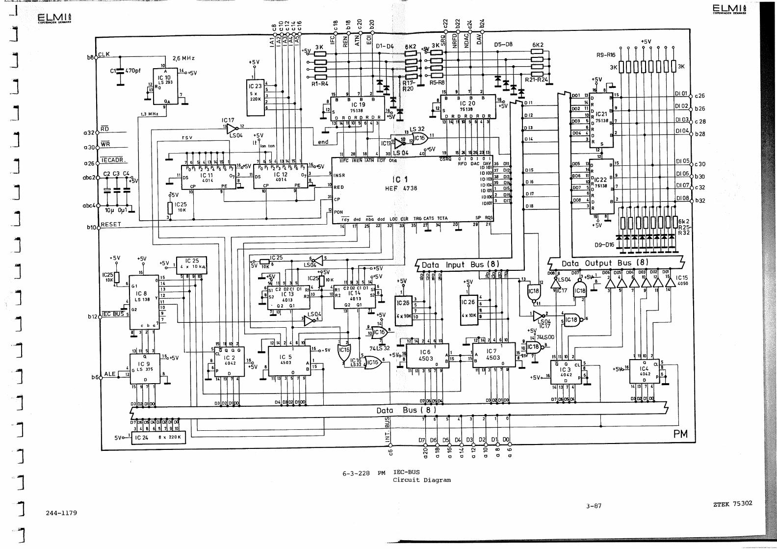
ELMCOPtNUAGN PtNM*fl
9
-
Q C”J 0- N (N
00L3UU 0 0 £
Q z Z —
w —
3K
R1-R6
15 9 7 2 --
B BIC 19
75138
RD RD R DR
C
6-3-228 PM IEC—BUSCircuit Diagram
5V
1BF0
R9
1C21o7513f
RD
7
2
15
9
7
2
-“
-
;lcAlo12 IC1S
8
417 1C18 3 5 7 9 ii 164050
0061fl UI)? 3 100b 005 006
12
6
51C18 6
15I1 2 2
Q 0 CL5 0 CL5IC3 8 16 1C4 8
5V 16 6062 6 6062
0 0
141376 161376
07 IX
ZTEX 75302
CLK216 MHz
(N (N(N (NU .
+5V
1C23
*4 -t(N (No
0u_ <cr Oz z
b8
a32
o30
026
obc2
abc6
blo
tsv
HE Ii,.
B
S0
B
1C17jojL—
LSO4 5V
•:—i
D5—D8 61<2
R2
IX
D1-04 61<2—ci °=
T cz:Hc:J; o-=
-H--,-1 °-=
R 1 7—__
. R20
Jv
_
LS 32_r- 11
IC17j -a-4t__.——
30 L504 60r5v 19
RD
IECADR.
C2 C3 C6
III+%v)TII
lop Opli
RESET
9 2
R9-R16
31<
131 1
1-c’I end
11
76 5 413116151 I 7 jSj6l 14Th I
F2 P P P5 % P7 1i045V p0 p1 p2 F;
IC 11 0713 11 OS 12 0y126016 8 4016 8
PE cp Pp
IC 075
R U R 0 R
•5V
3K
DI 01
I P0F*1
HIID510
t?5 V
n10K
3
1i.I 11
0 II
28
4
IS C
9
3
012
iTp TTi•ATFi 1ThY Ota
INSR
10
D0I 13
16D02 11
10003 5
6004 4
3
15
III
I
IIII
I
I
.o
013
016
132
I
c26
01R FD
,c IHEF 6738
L36 DII
37 012
38 01339 Di1 015
2 Dli3 017
CI 01DAC DAV
ID 101ID 102ID 10310106ID 105
ID 106I DI&7
cP
PON;: dvd nba dcd LOC CLR TRO CATS TCTA
015
+5V
IC2510
-
bl2.) BUSs
+ 5V
61
IC 8LS138 V
02
0 16
DI 02j b26
flIfl c28
0106b28
0105 c30
DI06 b30
D107 c32
DI08
5V 10K
D 17
I 17 2122 32 3:
12
12T
_j 0
005 II
—i IC22
::: 7S138
6 R2PL_ D
16
+ sv2j
6 5
LSO6
SP RQS
zi
0 8
29
IC 25
161312
1110 Ii-IL L.
211
4 Data
J I I IC25I1IoK+ 5V
.-I52
02 01rn-04I L7
b32
0IS
Input Bus (8)D
c09-016
C b a7
13 11 5 3Q 16
D3D D100
IC 9L0LS375
15 7 1
it
b 6.
+ 5v
15 1 IIS
IC 5L1J27J.J° 11 13 3 1
CLIC 26042
86503
Data Output Bus (8)
Li5V
I26 tEEI 18
[3f 52D2C1DI1C146013
2 01
+5V
j168
‘—1 12 14 2
76LS32+5y 1 IC6
B
6 I16,
I C 16
J18
1C17+ 5V
16 714S00
3oI1B8
D3f021DI
‘7
07 06 0IXJDJ0IJX
3 6 8 6! sI ij 9j1o1
5V0—9 IC26 8 x 220K
46 10
. .061031021 D1IIY3I
1’ 12 16
IC 76503
c— Data Bust 8)I. • _
_ T
S
071 106
U,
DC
244—1179
Dl
7 6S
z
CS S
07
210
(tJ0
-3
a(N
02 01 DO
U a
PM
3—87

ELMJCOHAO(N ONUA
TRI+NSISTORS
2N2907A
85545
2N2222A
DIODES SILICON
1N4448SEX 87 86V2
CONNECTORS
C11AO15P2ABB2
DB-25S-0L2
socxr
20 pins C932002
Heatsink 105259/10
PRINTER
National EUY-1 0E0 14-RE
Printed circuit Board
ELMIcoPeuw.G ONMK
c. ;
CIC
I;C[CCCCC[[CCC
Cir. Qty Stock No. Description Manufacturer
Re (Subject to change)
T1-8, 17
T9—15T16,
18—20
D1,3D2
97
4
21
11
1
2
1
1
TexasTelefunken
Texas
TexasPhi lips
lIT
Texas
Assmann
Matsushita
Elini6—3—266
6—3—266 PP Printer Interface
Electrical Parts List I
ZTEK 75302 3—90 246-1179
r

COPEN,flr.EU Of NU000
Cit. Qty Stock No. Description Manufacturer
Ref. (Subject to change)
CARBON FILM RESISTORS CR25 0.33W
1 OOR560R1K1KS3K94K?8K210K22K47K
2 322—2 11—131011356113102131521339213472138221310313223
13473
RESISTOR NTTWORKS
5 60R560R270Rlx11(2
4308R—101—561102—56 1102 —2 7 1101—102102—122
]]
I
i]
11
]
POTENTI0MTER CERMEI’
RiR2R3R4R5R6R7R8—1 1Ri 2—14
R15
IC8IC9—11ICI2, 16
Id 3114,15
P1
C2,11,12C8
C4C6C?
Cl ,10C3C5C9
IC11C21C3IC4‘CSIC6,7
111111
431
13212
1
3
111
2111
111112
500R type 3386 H
CAPACITORS CERAMIC
0,1 uF/16V
470 pF C052K471K2X5CA
Phi lips
Bourns
Bourns
Ferroperm
Kemet
Philips
Spaque
FrakoSprague
Texas
Fairchild
CAPACITORS, F)LYESTER
0,22 uF 2222—344—20224
D,022UF 20223
1,0 uP 20105
CAPACITORS, ELECTROLYTE
10 uF/1OV type 1500
2,2 uF/35V “
220 uF/40V EHF 220/401A
1 uF/1OV type 1500
WTEGRATED CIRCUITS
3N 741S 373J
3N 741S 74J
N 74L 121J
3N 741S 14J
3N 741S OOJ
zA 79M 24 ABC
L 1 242—1179
6—3—266 PP Printer Interface
Electrical Parts List II
3—91 ZTEX 75302

r.N1JJ
22 i TD 4-
— ‘ei
CC
[L
247-1179
6—3-266 PP Printer Interface
Electrical Parts Location
ZTEK 753023—92

ELMICOPENHAGEN DENMARK
2L... I_...IVI I SCOPENHAGEN DENMARK
cli
10p163Tov
__________ _______________________
Printer InterfaceCircuit Diagram
248—11793—93 ZTEK 75302
PRINTER: EUY —10E016 RE
3 15
I
5V
2 15
I3I
:&242
-30V1 16
böT6 ööT5 DOT4 nDOT3 DOT2DOT1)1._ I’
C2J Cli l2j
0,i1T0p1T0JT 560
c iC3 -
8Ti
iFi 1oT2J2I63V Ti —T7 2
*.24V2N2907A 1C12
5OR 4K7BSS ‘ ici
1K21
I
I I 1 1 1 I
tCB ICB tC8 1C8 1C8 1C8560 560 560 560 560 550
126
13 T4£
T5 T62
17
C 6 8 2 I 6 8
_______
1C12 ICi2 ICi2 1C15 I 1C15 1C15
1C1632703 ci27O 727o 1C15 270 ICl5f27° 1c1562707
1K2 i 1K2 6 1K2 5 1K2 1K2( 11<2 2
!C13 1C13 ICi3 2 1C13 Id 6 1C13i 110 11< 111 ,< Ti 1K T13 1K 116 i 115
1 1 1 1 1 1
I • S—
f45V201vcc
22
8207.
185
11
2
5
6
I
IcloD0Ti 3
PPL4i+______5 FPPi.7J IC1
‘ 7LS373
jf%sIC92Qii4M0T0R] 18
0 PI I Enable Conft GM)
PRENAB3JS46 1F
9
12
15
I
16
19
II
26
•NSV
11922A
I
r.C5
220i
I174
+5V
R12
PINSERT
22KR3
Di 1C6
1K
22r,
R23(A1 1C3
______
5V10
6A2350ps
CiaR9101<
560 76L121
7GND 0
MSTATUS
D3 R13
Icli221<
560
IC”
I
Ml
44
1C451C5 6 1
76 LS 00
____
117 C7‘ 1C5 -24V• lpI5OV
6Head common
I
Motor t-)
5
I
#5 V
161 10
6 Motor(
iiLfJ
1 6
1 Tf85V 2N2222A
Ru I!!
loKy
I
6—3-266 PP
Pick—up
21
PP’cg1JI
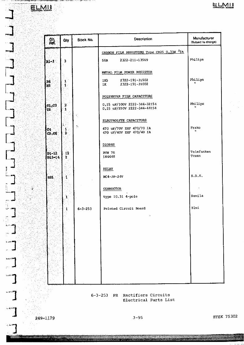
]
1IODES
BYW 761N4448
RELAY
NC4-JP-24V
cONNECrOR
type 10.31 4—le
6—3—253 PR Rectifiers Circuits
Electrical Parts List
ELMUDPflk4P1 t4MA*
LzLM!COP HGN
Cif Oty Stock No. Description Manufacturer
Ref tSubject to change)
CARBON FILM RESISTORS Type CR25 0,33W ±5%
56R 2322—211—13569
METAL FILM POWER RESISTOR
11411%
C1,C3c2
CS ,Cs
Dl —12D13-14
YIEI
IRS 2322—191—315021K 2322—191—31002
POLYESTER FILM CAPACITORS
0,15 up/bOY 2222—344—32154
0,15 uF/250V 2222—344—44154
ELECTROLYTE CAPACITORS
470 uF/70V ES? 470/70 IA
470 u?/40V ES? 470/40 IA
:3II
tJHH1H1
I11II1I
3
11
21
12
122
1
1
1
Philipa
Philips
Philips
Frako
Telefunken
Texas
S.O.S.
Davila
Printed Circuit Board Elmi6—3—253
249-1179 3—95 ZTEK 75302

ELMIELMI
COPENHAGEN DENMARK
COPENHAGEN DENMARK
Qty Stock No. Description Manufacturer
Re.(Subject to change)
CAR)N FIU.f RESISTORS type CR25 0.33W ±5%
R6 1 11(5 2322—211—13152 Philips
R7 1 21(2 13222
R8 1 15K 13153
R9 1 4K7 13472
RiO—li 2 100R 13101
R12—13 2 2R2 13228
R14 1 lOX 13103
TENTIOMETER CEBMET
Fl 1 lOOK 3386H—1—104 Bourns
CERPMIC CAPACITORS
C? 33 pF 2222—638—10339 Philips
C8—9 2 1.5 nF 630—03152
ELECTROLYTIC CAPACITOR TP,NTAL
ClO—li 2 10 uF/20V 1500 Spraque
INTEGRATED CIRCUIT
Id 1 MC 1468 GMotorola
TRPENSISTORES
Ti 1 2M2907 ASiemens
T2,T4 2 2N3054RCA
T3 1 2N5955RCA
ZENERDIODES
015 1 BZ X 87 C 33Philips
CONNECTOR
1 DR 25S1AONlET
1 Heat Sink 105259/10 Asmann
1 6-3—25 4 Printed Circuit Board Eimi
6—3-254 PS Power Supply
Electrical Parts List
:1
r:1’
LI
I
Ir
]
&5k
5k
3—96251—1179

ELMHCOIIMUAGEW DENMARK
ELMICOPENHAGEN DENMARK
ZTEK 75302
6—3—253 PR Rectifiers Circuits
Electrical Parts Location
3—97
•1
1
11
1250—1179
s- .4 •-
U
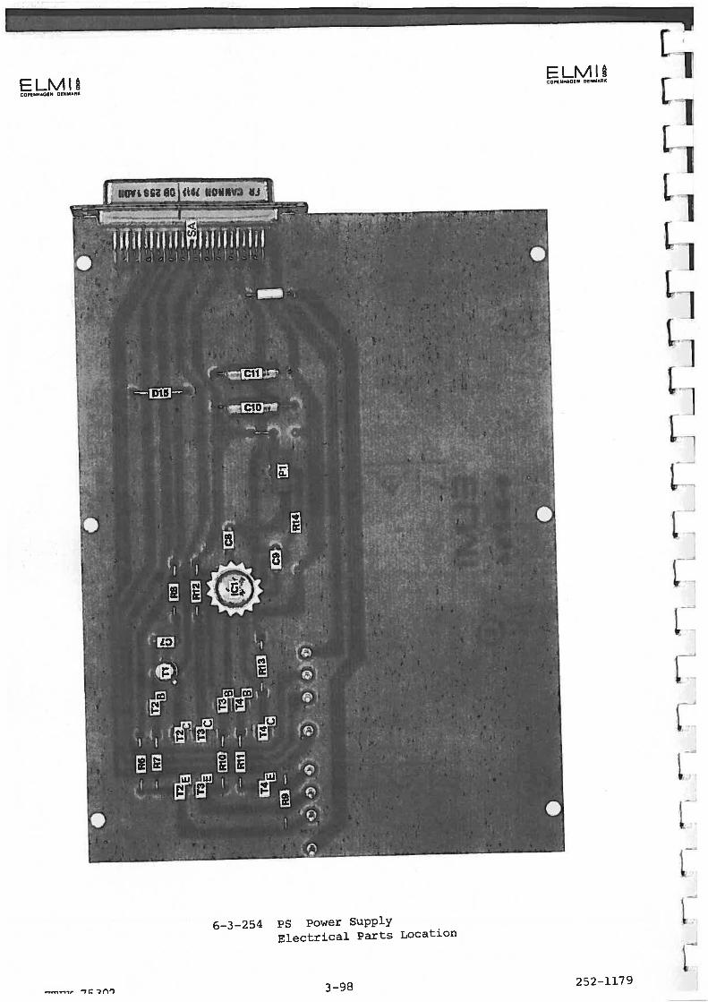
C’Pfl!flK
MA P A
I HoYt scz edjf!L NONNVO I
6-3—254 PS Power Supply
Electrical Parts Location
7Cn’) 3—98 252—1179

U) N ‘-3 tn
-4 -7 — 0 -7 to -7
(‘.7 > -4 Ui
> -4
——
——
——
——
—
.‘
LJ
L_
1L
_i
L.a
L_i
Ui
Ut
Ut
Ut
__
__
__
__
H ‘-I
1-’ U,
U)
CD 0 H Hi
H CD
.
HH &
t.rt U,
Cl)
0 CD H U)
H 1<
—3
U,
U)
0 C’)
Lr
-
I‘°
;4;
n;)
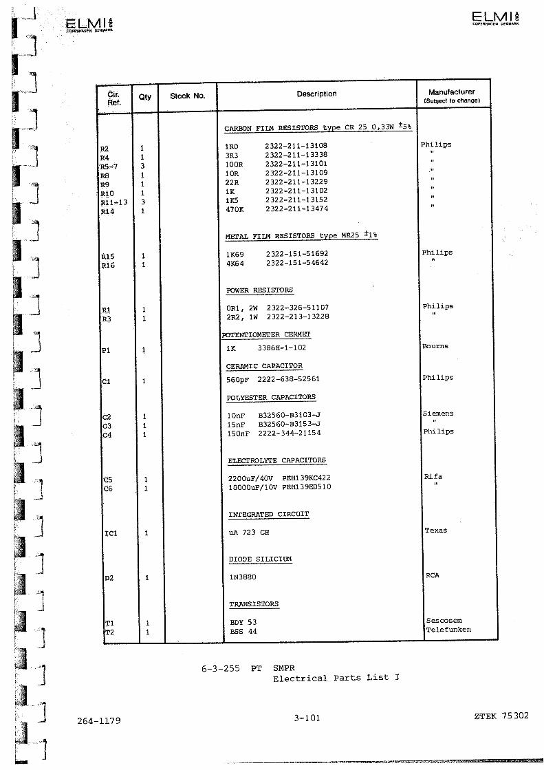
1
3
ELMflCQPENAGEN ØENMAK
ELMHcOPr.HAGt. DENMA
Cit. Qty Stock No. Description Manufacturer
Ref. (Subject to change)
R2R4R5—7RBR9RiOR11—13R14
CAR)N FILM RESISTORS type CR 25 0,33W ±5%
1RO 2322—211-131083R3 2322—211—13338100R 2322—211—13101
1OR 2322—211—1310922R 2322—211—132291K 2322—211—131021K5 2322—211—13152
470K 2322—211—13474
METAL FILM RESISTORS tvDe MR25 ±1%
R15R1 6
RiR3
Pt
1K69 2322—151—51692
4K64 2322—151—54642
POWER RESISTORS
OR1, 2W 2322—326—51107
2R2, 1W 2322—213—13228
POTENTIOMETER CERMET
lx 33863—1—102
CERNIC CAPACITOR
560pF 2222—638—52561
POLYESTER CAPACITORS
Ci
11311131
11
11
1
1
111
11
1
1
11
C2C3C4
1 OnFl5nFl5OnF
Philips
Phi lips
Philips
So urns
Philips
Siemens
Phi lips
Rifa
Texas
RCA
SescosemTelefunken
B32560—B3103—J
332560—B3153—J
2222—344—21154
C6
Id
D2
ELECTROLYTE CAPACITORS
2200uF/40V PEEl 39KC422
l0000uF/1OV PEH139ED51O
INTEGRATED CIRCUIT
uA 723 CR
DIODE SILICIUM
1N3880
TRANSISTORS
BDY 53BSS 44
TiT2
6—3-255 PT SMPR
EleCtrical Parts List I
264—1179 3—101 ZTEK 75302

TRANSISTORS
2N2222A2N2907A
TYRISTOR
S 2600 B
ZENER DIODES
BZX 79 CS V6
BZX 87 ClO
CIE)KE
Type l,25KP, 14862
HEAT SINKS
5K 37/30/SAUK 35/SA-3
CONNECI’OR
C42 334—Al 91—A202
Printed Circuit Board
r
[.[V
F
ELMHCGflWHAG(N OENUAfl
ELMICOPtNH&GEN O(NU*RK
T3T4
Cfr. Qty Stock No. Description ManufacturerRe. Subj to cbange)
D3D4—5
11
1
12
1
11
1
1
Li
Simensft
RCA
Phi lips
J. Schou
Fischer
Siemens
Elmi6—3—255
6—3—255 PT SMPRElectrical Parts List II
ZTEK 75302 3—102 265—1179

11
1
1
Ij
II-7
]
1
1]I
]6—3—255 PT SMPR
Electrical Parts Location
6-3-255 PT SMPR
Circuit Diagram
j 266—11793—103 ZTEK 75302

ELMICOPENHAGEN DENMARK
ELMICDPENHLGEN DENMARK
6-1-229 PN Mother BoardcircUit Diagram
266—1179 3—105 ZTEK 75302
-15 V
OVa
—15V
ISVICHASSIS I
cOK.ItCmR SVFOR
*
ra KAA OVd
KEY
tED
7Y
FOR POWER SUPPLY
OVa
SV tMicxDl
DL
DI
0€
INRJT
DVd III
a5
IS
12
IL
DIG
aIB
Q20
IfIII III
Ii
AD OKE oNRE AR04 OR
5V OVd
?SV
OVU
SUPS
5V
5V
OVU
5V OdDO
DI
02
03
DL
05
06
07
III I I III III
IZCDVc3
I
1II
II
N
S •
GNIDH*IOW -$0 RHo ENdISV 5V0 qL_ isv sv0
oiqL_1 i
02 !ii 02
03 —I 03
DLq&_I DL
05 —4 05
D6L4 E
O7—$ 0
MICRO-PROCESSOR
02 OKND NOCD tL
5V OWlC
DI
02
03
cx.05
06
07
IEC -
BUS
S
h_
.fS !AI
.iO 1A2
+2 1A3
5L lAL
.!5 165
4L REN
._i6 IFC
.O LOT
.ATN
522NRFD
t!22Kr SRQbIL
DAV
.? NOAC NOW
._60202
4? ooi.6
DIOL
p RAE
0206 65
c!3Oom5
.?0107 tto
K]
02 at
02 Ct
5V OvaC
0
02
Dl
DL
DI
0€
DY
MEMORY
S
S
65
S
alp
a12
lL
:116
a18
aID
SEC TES
51
FORREARTEAM IGIS
a15
o13
05
07
aS
all
al9
c5
lJ
I C22
c6
D c21.
12
32 EKENY c29— TERIE —
30RAtS
AID
bG
SFOR REARCE RU IN A IS
5V
A2
86
Al
83
Al
All
82
R52
81
551
553
OVd
556
552
lv
RSl
RESET IN
RS6
COOlER
TIIH
scPPATIS
DAd
MO1
AID ENTO
CARl OJ
nms tT
AtE XC
65
RESET 0017
IU007
EEC COP lEtCEO TEOR
2 INPUT
6 3
S 5
8 7
0
2 1
IL 13
15 OVA
I6
o6 c6
10 tiC
0121012
114014I
16 c15
DISbCiBI
a20c20
b2l
c21
/jo
c22
c23
b23
4
44POWER 7
L!!_/ C26
4/2
43 I
FOR FRONT WARD
*D OK
RD NO02 CL
lv OVAcxDI
02
03
DL
05
05
07
OSCILLAl
t PART Al
S
03
03
00
00
T0
T1
S15
I
VaYl
‘12
53
54
aSCiI,
06C111
OSC2I6
DSC2JI
46
67
68
CO
a29
all
dO
oil
cl2
c13
616
cl5
615
c17
cIB
619
!Li1t
UFENNY
FOR REARTEOHINALS
‘5
o6
DATA aSBUS
091
aiD
ali
al25!
aWl4
r
All
81
81
8279*2
1651t1 BO
Iai 553
00Z21D B2l9
006id; 552026
E6i;i 83
MEWOCUIRSI25
Al
a26
Wil[A\
ATiz
65O 86
CEEBUS Al a29
656651 B
AL b29
SUWI B2
KOOK 5S 32
1117805 81
nS3b32
8_3
L*i ssiELK K
85 a3i c_S
WE A3 °i\ 616
RESET A2 bIG cB
01K R5 c12
FOR FREN4T WARDS
—30V OVA_RI\
CL
-
OR:1
A
K
SFOR PRINTER
S
a6 CS
aS c
alO CE
al2 CI
alL ci
a16 CIS
aIS ci
a2O c21
c22 a2€
a
-i28
26
22
22
26
RICNd I ENd OUIDEN I DOdqL__4 ISV IV —i isv WD
I
Q___—4 Dl aS I
aiq___4 —I 02 aiD
i2___4 —A 03a12
aj____1___ 06 alL
!L__4 ___. 05a16
!L_A —4 06 alS
022__ __4 07 020
SaUATORS GEERATOR
(FWRTBI TEST
S S
l8cl83
:ZQ___S 03
:L_s
:!L_si’
?L_s T0
b_Z r1
:___,
L_P ii
b2
1
a26b26 ySTART 12CONV
___p_ LEELffREa!
Yl
701551 NP -
i 0SOF
:112 osco rsis c 1’a!
alS SIGN1
9 0A2 UEASWII
D4l
PKDP.NW*• Colafrol Itn.N
TT9thltJl
06CI
S
AU 32I1
ArT OUT 1
SIGNI2.6
061
bG
,8
bID
b12
al
hi
b3
a3
al3
alL
Cl
c13
dl
CS
93
93
biS
cl2
67
CS
Cli
ClO
93
TTEMJ4T
OSC 2
S
%TT32dB2
ATTOUT2
__2Z6 SIGN2
_s: DA2
_sa° OSC2ON
ATT2
IIaJ31
- DIN DOd
0315v lv
DI
02
Dl
04
06
06
07
REC our/ FRENNITERI4I
GEN IN
QNN
GENE
Jj.PENS
JFIDEN 6
OEN.3
RTT bI6IIDOdOl —e-—.
NIT 0042 1511DUO,
tidK268141
DUID
0%
bjOwJ 26 I
111‘
ENLSD$1
jSlWUN
5V
FOR I1ARTE4INAS
Rl
5279*l
Rill
517
512
516
513
RL5
OVA
514
OSC1OR
fi9
r
==__:ER

No aux. signal or wrong level
of aux. signal
Wrong pulse or pause
Wrong time measurement
IEC-Bus
No or wrong communication
Display/Keyboard
Wrong output of all displays
or LEDs
No flashing of LEDs or decimal
pointsNo key input
Wrong lighting of one display
Imp1ifier
Aux. signal switch
Tone burst control
4 kHz oscillator
Tone burst control
Connector
IEC-Bus interface
Connectors
Decoding, driving or
display circuits
Decoding circuits,
driving circuits or
LED
Decoding circuits,
driving circuits or
LED
PAPA
PJPD
PJrear
PMrear
PK,PL
PKP1
SYMPTOM PROBABLE SOURCE BOARD
External tone burst
modulation of no effect
Receiver Test Input
Wrong active level of input
No reading of input
Test input reference
Test input
Connectors
4 kHz oscillator
PJ
pJrear, front
PD
Printer
Lack of dots in print-out
No or wrong print—out
CL
[I
L
L
IDot drivers
Printer portsPrinter interface
Interface circuits
PP
PJPP
PG
Wrong lighting of one result LED
Wrong lighting of one key LED P1
ZTEK 75302 4—2 197—1179

ELMICOPENHAGEN DENAAN ELMU
COPENHAGEN DENUAAH
ii
E]
ii
SYMPTOM PROBABLE SOURCE BO2RD
No reading of one key Decoding circuits PLor key
Power Supply
No or wrong +15 V, -15 V, -30 V Rectifiers PRRegulator PS
No or wrong ÷5 V Rectifiers PRSvitch-mode power PTsupply
No voltages Transformer modulePower relays PRPower key PLFuses
Program Execution
Wrong program execution Microprocessor PGMemory PH
Some troubles may, however, stem from ment are described in the sectionthe connections on the motherboard PS. ‘Specifications’ in the ‘Operator’s
Manual’.
11.2 PERFORMANCE CHECKTest Equipment Required
The performance check procedure may beused for checking the features ensuring A satisfactory performance checkcorrect performance of the instrument, requires a minimum amount of testThe limits and demands for accuracy equipment as follows:which must be observed by the instru
DESCRIPTION MINIMUM SPECIFICATIONS PURPOSE
Sine generator
DC—generator
AC- voltmeter
Frequency range:200 Hz — 6000 Hz
Level range:10 mVrms - 20 Vnns
O V - 10 V
Range:10 mVrms - 20 Vrms
Accuracy:1%
To send measuring toneof Generator Test.
To set input levelof Receiver Test.
To measure level ofGenerator Test andReceiver Test.
198—1179 4—3 ZTEK 75302

CE
DESCRIPTION MINIMUM SPECIFICATIONS PURPOSE
Input impedance:> 1 MQ
DC-voltmeter Range: To measure input level1 V — 10 V of Receiver Test.
Accuracy:5%
Selective voltmeter Range: To measure harmonics
60 d3 of Receiver Test.
(Band width: 500 Hz)or Accuracy:
1 dB
High—pass filter 60 dB/octave To measure harmonicsof Receiver Test.
Frequency counter Range: To measure frequency
200 Hz — 6000 Hz of Generator Test andAccuracy: Receiver Test.
0.1 Hz
Oscilloscope Time division: To measure1 ms — 100 ms tone bursts of
Receiver Test.
[ii
[I[iJ
Generator Test Performance (Boards PA, PD)
a. Connect the sine generator, the AC—
voltmeter and the frequency counter
to Generator Test Input 1.
b. Press HOW, FREQUENCY, LOAD and WAD.
c. Check that the frequency measuredcorresponds to the measurement of
the frequency counter.
d. Press LEVEL.
e. CHECK that the level measured cor
responds to the measurement of the
AC-voltmeter.
If the Receiver Test Output performance
fulfils the specifications, the Genera
tor Test performance may be checked bymeans of a self—test (see the ‘Operator’s Manual’, section 3.1).
ZTEK 75302 4—4
Receiver Test Output Performance
1) Frequencies of Signal Generators(Boards PE, PF)
a. Connect the frequency counter tothe Receiver Test Output.
b. Press FUNCTION and enter the parameters with the values wanted, butturn off oscillator 2 and set PAUSEat 0 ms.
c. Check that the frequency measuredcorresponds to the parameter valueread in.
d. Repeat a., b.., and c. with oscilla
tor 1 turned off instead of oscillator 2.
2) Harmonic Distortions (Boards PB, PC).
a. Connect the selective voltmeter (orthe high—pass filter and the AC—vol—meter) to the Receiver Test Output.
199—1179

dJi
b. Press FUNCTION and enter the parameters with the values wanted, butturn off oscillator 2 and set PAUSEat 0 ins.
c. Check that the level of harmonicsof the oscillator 1 signal is 46 dBlower than the level of the fundamental.
d. Repeat a.,, b. and c. with oscillator 1turned off instead of oscillator 2.
3) Output Level of Signal Generators(Boards PA, PE)
a. Connect the AC—volmeter to the Receiver Test Output and terminateby 600 . Set the impedance switchat 600 2.
b. Press FUNCI’ION and enter the parameters with the values wanted, butset the output level at 15 dBm,turn off oscillator 2 and set PAUSEat 0 ms.
k:I
] c. Check that the level measured is 15dBm.
d. Repeat a., b. and c. with oscillator] 1 turned off instead of oscillator 2.
] 4) Attenuators (Boards PB, PC)
a. Connect the AC-voltmeter to the Re
] ceiver Test Output and terminateby 600 Q. Set the impedance switchat 600 .
1
b. Press FUNCTION and enter the parameters with the values wanted, butturn off oscillator 2 and set PAUSEat 0 ms.I
C. Check that the level measured cor— -
responds to the parameter valueread in at the following output levels: 14, 13, 12, 11, 8, 7, 0, —1,—16, —17, —48 and —49 dBm.
d. Repeab a., b. and c. with oscillator1 turned off instead of oscillator 2.
5) Aux. Signal Input (Board PA)
a. Connect the sine generator to theAux. Signal Input (rear panel) andthe AC—voltmeter to the ReceiverTest Output.
b. Press FUNCTION and enter the parameters, but turn off both oscillators and set PAUSE at 0 ms.
c. Check that the attenuation of theaux. signal is 0 dB.
6) Tone Burst (Boards PD, PJ)
a. Connect the oscilloscope to the Receiver Test Output.
5. Press FUNCTION and enter the parameters with the values wanted.
c. Check that the length of pulses andpauses is correct.
If the Generator Test Performance fulfils the specifications, Test Nos. 1,3, 4 (partly) and 5 may be made bymeans of a self—test (see the ‘Operator’s Manual’, section 3.1).
Receiver Test Input Performance
a. Connect the DC—generator to the Receiver Test inputs 1-8 and the reference ground (terminal 9). Connectthe DC—voltmeter across the generator.
b. Press FUNCTION and enter the parameters with arbitrary values.
c. Check, by means of the result LEDs,that the active level of input iscorrect (note that the measurementmust start with input levels beingnon—active).
14,3 ADJUSTMENT
Each printed circuit board is individually adjusted at the factory. If,therefore, a board needs replacement,no adjustment of the instrument willbe necessary.
E1
11LI I
ZTEK 75302 4—5 200—1179

If, in the course of time, the instru
ment needs adjustment, the following
guidance may be used:
Test Equipment Required
A satisfactory adjustment requires a
minimum amount of test equipment.
Level Measurement Adjustment
(Generator Test) - Board PD
1) AC/DC-Converter Symmetry
a. Reset the instrument.
b. Apply a tone to Test Point 1, TP1
(10 kilz square—wave, approx. 1 Vrms)
c. Measure the Ac-voltage of TP2.
d. Adjust P1 to the minimum Ac-voltage
of TP2 fapprox. 10 mVrms).
In addition, an extension board with
a 96—terminal DIN-plug will be needed,
which can be purchased from E1141 A/s.
2) Offset and Gain
a. Apply a tone to Generator Test In
put 1 (1 kHz sine, approx. 0.7 Vrms).
b. Make a Generator Test Frequency
measurement on generator No.1
c. Adjust the generator until the TPS
voltage shows 6.887 Vrms (correspon
ding to 0.0 dBu at the Generator
Test Input).
d. Ground TP4 (the MFE will now show
the output frequency of the V/F-con
verter).
C
ELMICOPENHAGEN CENUARX
ELMICOPENHAGEN DENMARK
DESCRIPTION MINIMUM SPECIFICATIONS PURPOSE
Sine/square—wave Frequency range: To send measuring tone
generator 1 kHz — 10 kHz of Generator Test.
Level range:
0.1 Vrms - 1 Vnns
AC—voltmeter Range:To measure level of
10 mVrms - 10 Vnns Generator Test.
Accuracy: To measure output impedance
0.1%and output level of
Input Impedance: Receiver Test.
> 1 M
DC-voltmeter Range:To measure power supply
1 V — 20 V voltages.
Accuracy:
1%
Selective voltmeter Range:To measure harmonics
60 dBof Receiver Test.
(Band width: 500 Hz)
or Accuracy:
1 dB
High—pass filter 60 dB/octave To measure harmonics of
Receiver Test.
F
11
[zIJ[j
1[1
CC
7P1( 702 4—6201—1179

ELMI
e. Ground TP3 and adjust P2 until the
result display shows 337.4 Hz.
f. Remove the ground from TP3 and adjust P3 until the result displayshows 6000.0 Hz.
g. Repeat e. and f. until adjustment
is no longer necessary.
Output Impedance
(Receiver Test) - Board PA
a. Make a Receiver Test measurementwhere OSC1 = 950 Hz, 15 dBm (freq.series 2, rec.comb. = f2/f4, deviation 1 50 Hz).OSC2 OFF; PULSE = 10 Ins; PAUSE0 ms.
b. Set the impedance switch at 600Q.
C. Measure the voltage at the ReceiverTest Output.
d. Place a 600Q resistor f 0.1%) acrossthe output and adjust P1 until thevoltage is half (±o.1%) the voltagemeasured under c.
e. Set the impedance switch at 8001and remove the 600Q resistor.
f. Measure the voltage at the ReceiverTest Output.
g. Place an 800 2resistor (0.1%) acrossthe output and adjust P2 until thevoltage is half (±0.1%) the voltagemeasured under f.
Hazmonic Distortion
(Receiver Test)- Boards PB, PC
a Make a Receiver Test measurementwhere OSC1 = 2500 Hz, 15 dBm (freq.series 12, deviation 1 = 100 Hz).OSC2 = OFF; PULSE = 10 ms; PAUSE =0 Ins.
b. Measure the level of the 3rd harmonic (7500 Hz) and adjust P1 (boardPB) to the minjmujn level of thatharmonic (typically between -50 dBmand -60 dBm).
Output Level
(Receiver Test) — Board PB
a. Make a Receiver Test measurementwhere OSC1 = 950 Hz, 15 dBm (freq.series 2, rec. comb. = f2/f4, deviation 1 = 50 Hz)OSC2 = OFF; PULSE = 10 ms; PAUSE0 ms.
b. Place a 600 resistor (o.1%) acrossthe Receiver Test Output and adjustP1 until the output voltage is4.356 V (= 15 dBm).
c. Make a Receiver Test measurementwhere OSC1 = OFFOSC2 = 950 Hz, 15 dBm (freq. series2, rec. comb. = fl/f2, deviation2 = 50 Hz)PULSE = 10 ms; PAUSE = 0 Ins.
a. Repeat b. with P2.
Printer - Board PP
Cleaning and paper roll installationprocedures are described in the ‘Operator’s Manual’ (section 3.2).
The printing quality can be adjustedby means of P1.
Power Supply - Boards PS, P11
±15 V can be adjusted by means of P1on the board PS.
+5 V can be adjusted by means of P1on the board Pr.
202—1179
]4—7 ZTEK 75302
ELMICOPENHAGEN OENU*Ok
c. Turn P1 further to the left (counter-clockwise) until the signal hasincreased by 2 dB.
d. Make a Receiver Test measurementwhere OSC1 = OFFOSC2 = 2500 Hz, 15 dBm (freq. series12, deviation 2 = —100 Hz)PULSE 10 Ins; PAUSE = Oms
e. Repeat b. and c. with P1 on boardPC.

5 REPLACENENT PARTS
Orders for replacenient parts should To order replacement parts, address
include information on: order or inquiry either to yourlocal reprensentatjve or to:
a) Type and serial number of instru
ment.
I) Circuit reference. ELMI A/Sc) Description
90, Kitkebjetg Alle
The type and serial number appear from DK-2600 GLOSTRUP
a small sign on the rear panel of the
instrument, whereas circuit references Denmark
and descriptions may be found in the
component lists.Phone: National: 02—45 42 11
To order a part not listed in the corn- International + 45 2 45 42 11
ponent lists, give a complete descrip
tion of the part and include its func— Telex: 33 423 ELMI DK
Uon and location.Cable:;: ELMIWORKS
203—1179 5—1 ZTEK 75302