multi-cd control high power cd/mp3/wma player with...
TRANSCRIPT

PIONEER CORPORATION 4-1, Meguro 1-chome,PIONEER ELECTRONICS (USA) INC. P.O. Box 1760, LonPIONEER EUROPE NV Haven 1087, Keetberglaan 1, 912PIONEER ELECTRONICS ASIACENTRE PTE. LTD. 253
PIONEER CORPORATION 2005
DEH-P6700MP/XM/EW
Meguro-ku, Tokyo 153-8654, Japang Beach, CA 90801-1760, U.S.A.
0 Melsele, BelgiumAlexandra Road, #04-01, Singapore 159936
ORDER NO.
CRT3435
MULTI-CD CONTROL HIGH POWER CD/MP3/WMA PLAYER WITH RDS TUNER
DEH-P6700MP/XM/EW
This service manual should be used together with the following manual(s):
Model No. Order No. Mech.Module Remarks
CX-3158 CRT3394 S10.1AAC CD Mech. Module : Circuit Description, Mech. Description, Disassembly
For details, refer to "Important Check Points for Good Servicing".
K-ZZA. FEB. 2005 Printed in Japan

C
D
F
A
B
E
1 2 3 4SAFETY INFORMATION
This service manual is intended for qualified service technicians; it is not meant for the casual do-it-yourselfer.Qualified technicians have the necessary test equipment and tools, and have been trained to properly and safelyrepair complex products such as those covered by this manual.Improperly performed repairs can adversely affect the safety and reliability of the product and may void the warranty.If you are not qualified to perform the repair of this product properly and safely, you should not risk trying to do soand refer the repair to a qualified service technician.
1. Safety Precautions for those who Service this Unit.
• When checking or adjusting the emitting power of the laser diode exercise caution in order to get safe, reliable
results.
Caution:
1. During repair or tests, minimum distance of 13cm from the focus lens must be kept.
2. During repair or tests, do not view laser beam for 10 seconds or longer.
2. A “CLASS 1 LASER PRODUCT” label is affixed to the
bottom of the player.
3. The triangular label is attached to the mechanism
unit frame.
4. Specifications of Laser Diode
Specifications of laser radiation fields to which human access is possible during service.Wavelength = 800 nanometers
CLASS 1LASER PRODUCT
- Service Precaution1. You should conform to the regulations governing the product (safety, radio and noise, and other regulations), and should keep the safety during servicing by following the safety instructions described in this manual.2. Before disassembling the unit, be sure to turn off the power. Unplugging and plugging the connectors during power-on mode may damage the ICs inside the unit.3. To protect the pickup unit from electrostatic discharge during servicing, take an appropriate treatment (shorting-solder) by referring to "the DISASSEMBLY".4. After replacing the pickup unit, be sure to check the grating.
CAUTIONDanger of explosion if battery is incorrectly replaced.Replaced only with the same or equivalent type recommended by the manufacture.Discord used batteries according to the manufacture's instructions.
DEH-P6700MP/XM/EW21 2 3 4

C
D
F
A
B
E
5 6 7 8
[Important Check Points for Good Servicing]In this manual, procedures that must be performed during repairs are marked with the below symbol.Please be sure to confirm and follow these procedures.
1. Product safety
Please conform to product regulations (such as safety and radiation regulations), and maintain a safe servicing environment by following the safety instructions described in this manual.
1 Use specified parts for repair.
Use genuine parts. Be sure to use important parts for safety.
2 Do not perform modifications without proper instructions.
Please follow the specified safety methods when modification(addition/change of parts) is required due to interferences such as radio/TV interference and foreign noise.
3 Make sure the soldering of repaired locations is properly performed.
When you solder while repairing, please be sure that there are no cold solder and other debris.Soldering should be finished with the proper quantity. (Refer to the example)
4 Make sure the screws are tightly fastened.
Please be sure that all screws are fastened, and that there are no loose screws.
5 Make sure each connectors are correctly inserted.
Please be sure that all connectors are inserted, and that there are no imperfect insertion.
6 Make sure the wiring cables are set to their original state.
Please replace the wiring and cables to the original state after repairs.In addition, be sure that there are no pinched wires, etc.
7 Make sure screws and soldering scraps do not remain inside the product.
Please check that neither solder debris nor screws remain inside the product.
8 There should be no semi-broken wires, scratches, melting, etc. on the coating of the power cord.
Damaged power cords may lead to fire accidents, so please be sure that there are no damages.If you find a damaged power cord, please exchange it with a suitable one.
9 There should be no spark traces or similar marks on the power plug.
When spark traces or similar marks are found on the power supply plug, please check the connection and advise on secure connections and suitable usage. Please exchange the power cord if necessary.
0 Safe environment should be secured during servicing.
When you perform repairs, please pay attention to static electricity, furniture, household articles, etc. in order to prevent injuries. Please pay attention to your surroundings and repair safely.
2. Adjustments
To keep the original performance of the products, optimum adjustments and confirmation of characteristics within specification.Adjustments should be performed in accordance with the procedures/instructions described in this manual.
4. Cleaning
For parts that require cleaning, such as optical pickups, tape deck heads, lenses and mirrors used in projection monitors, proper cleaning should be performed to restore their performances.
3. Lubricants, Glues, and Replacement parts
Use grease and adhesives that are equal to the specified substance. Make sure the proper amount is applied.
5. Shipping mode and Shipping screws
To protect products from damages or failures during transit, the shipping mode should be set or the shipping screws should be installed before shipment. Please be sure to follow this method especially if it is specified in this manual.
DEH-P6700MP/XM/EW 35 6 7 8

C
D
F
A
B
E
1 2 3 4
CONTENTS SAFETY INFORMATION..................................................................................................................................... 21. SPECIFICATIONS ............................................................................................................................................ 52. EXPLODED VIEWS AND PARTS LIST ............................................................................................................ 6
2.1 PACKING ................................................................................................................................................... 62.2 EXTERIOR................................................................................................................................................. 82.3 CD MECHANISM MODULE..................................................................................................................... 10
3. BLOCK DIAGRAM AND SCHEMATIC DIAGRAM.......................................................................................... 123.1 BLOCK DIAGRAM ................................................................................................................................... 123.2 OVERALL CONNECTION DIAGRAM(GUIDE PAGE).............................................................................. 143.3 KEYBOARD UNIT.................................................................................................................................... 203.4 CD MECHANISM MODULE(GUIDE PAGE) ............................................................................................ 22
4. PCB CONNECTION DIAGRAM ..................................................................................................................... 324.1 TUNER AMP UNIT................................................................................................................................... 324.2 KEYBOARD UNIT.................................................................................................................................... 364.3 CD CORE UNIT(S10.1) ........................................................................................................................... 384.4 PANEL UNIT ............................................................................................................................................ 40
5. ELECTRICAL PARTS LIST ............................................................................................................................ 416. ADJUSTMENT ............................................................................................................................................... 47
6.1 CD ADJUSTMENT................................................................................................................................... 476.2 CHECKING THE GRATING AFTER CHANGING THE PICKUP UNIT .................................................... 496.3 ERROR MODE ........................................................................................................................................ 51
7. GENERAL INFORMATION............................................................................................................................. 527.1 DIAGNOSIS ............................................................................................................................................. 527.1.1 DISASSEMBLY ..................................................................................................................................... 527.1.2 CONNECTOR FUNCTION DESCRIPTION.......................................................................................... 557.2 PARTS...................................................................................................................................................... 567.2.1 IC .......................................................................................................................................................... 567.2.2 DISPLAY ............................................................................................................................................... 657.3 OPERATIONAL FLOW CHART ............................................................................................................... 667.4 CLEANING............................................................................................................................................... 67
8. OPERATIONS ................................................................................................................................................ 68
DEH-P6700MP/XM/EW41 2 3 4

C
D
F
A
B
E
5 6 7 81. SPECIFICATIONS
DEH-P6700MP/XM/EW 55 6 7 8

C
D
F
A
B
E
1 2 3 42. EXPLODED VIEWS AND PARTS LIST
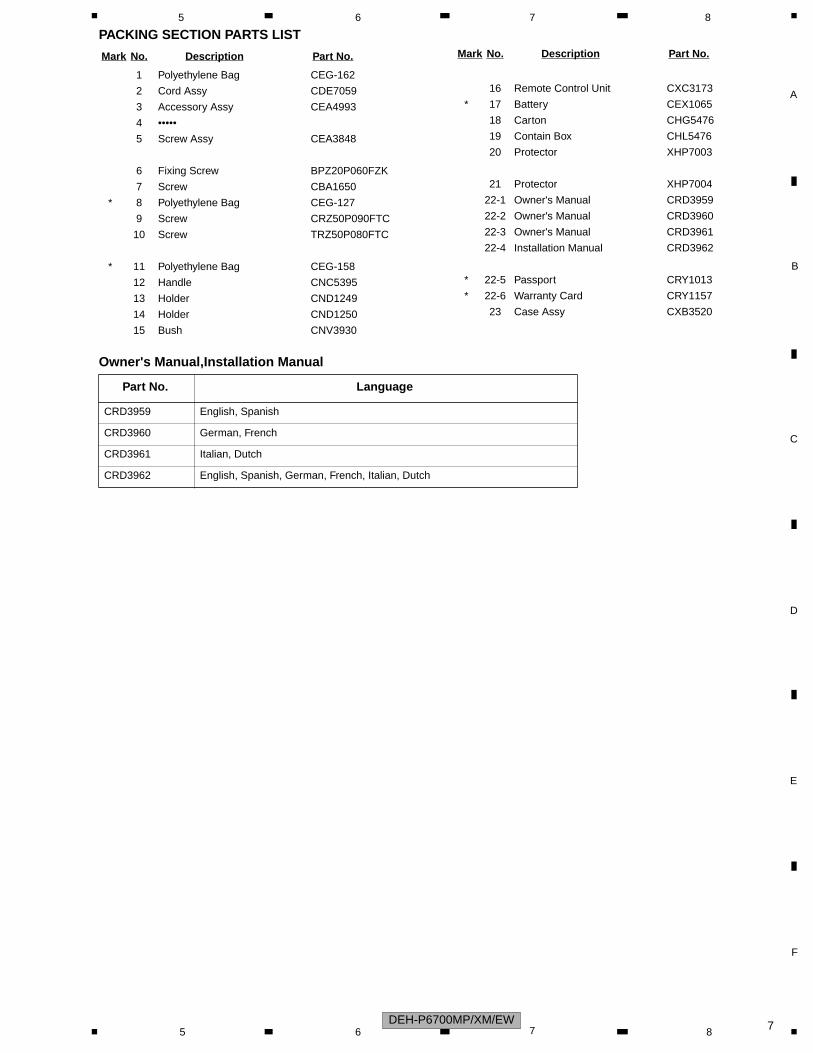
2.1 PACKING
NOTES : • Parts marked by " * " are generally unavailable because they are not in our Master Spare Parts List. • The > mark found on some component parts indicatesthe importance of the safety factor of the part. Therefore, when replacing, be sure to use parts of identical designation.
• Screw adjacent to mark on the product are used for disassembly.• For the applying amount of lobricants or glue, follow the instructions in this manual. (In the case of no amount instructions,apply as you think it appropriate.)
"
DEH-P6700MP/XM/EW61 2 3 4
C
D
F
A
B
E
5 6 7 8
PACKING SECTION PARTS LIST
Owner's Manual,Installation Manual
Mark No. Description Part No.
1 Polyethylene Bag CEG-162
2 Cord Assy CDE7059
3 Accessory Assy CEA4993
4 •••••
5 Screw Assy CEA3848
6 Fixing Screw BPZ20P060FZK
7 Screw CBA1650
* 8 Polyethylene Bag CEG-127
9 Screw CRZ50P090FTC
10 Screw TRZ50P080FTC
* 11 Polyethylene Bag CEG-158
12 Handle CNC5395
13 Holder CND1249
14 Holder CND1250
15 Bush CNV3930
16 Remote Control Unit CXC3173
* 17 Battery CEX1065
18 Carton CHG5476
19 Contain Box CHL5476
20 Protector XHP7003
21 Protector XHP7004
22-1 Owner's Manual CRD3959
22-2 Owner's Manual CRD3960
22-3 Owner's Manual CRD3961
22-4 Installation Manual CRD3962
* 22-5 Passport CRY1013
* 22-6 Warranty Card CRY1157
23 Case Assy CXB3520
Mark No. Description Part No.
Part No. Language
CRD3959 English, Spanish
CRD3960 German, French
CRD3961 Italian, Dutch
CRD3962 English, Spanish, German, French, Italian, Dutch
DEH-P6700MP/XM/EW 75 6 7 8

C
D
F
A
B
E
1 2 3 42.2 EXTERIOR
DEH-P6700MP/XM/EW81 2 3 4

C
D
F
A
B
E
5 6 7 8
EXTERIOR SECTION PARTS LIST
Mark No. Description Part No.
1 Screw BMZ30P040FZK 2 Screw BSZ26P060FTC 3 Screw BSZ30P060FTC 4 Screw BSZ30P200FTC 5 Cord Assy CDE7059
6 Cap CKX-003 7 Cable CDE7189 8 Earth Plate CNC8915 9 Insulator CNM7682 10 Cushion CNM8890
11 Tuner Amp Unit CWM9790 12 Screw ASZ26P060FTC 13 Screw BPZ26P080FTC 14 Screw BSZ26P160FTC > 15 Fuse(10A) CEK1208
16 FM/AM Tuner Unit CWE1645 17 Holder CND1054 18 Pin Jack(CN351) CKB1054 19 Plug(CN981) CKM1376 20 Connector(CN101) CKS3408
21 Plug(CN831) CKS3537 22 Connector(CN721) CKS3837 23 Connector(CN671) CKS4124 24 Antenna Jack(CN401) CKX1056 25 Holder CND1352
26 Heat Sink CNR1668 27 Terminal(CN402) VNF1084 28 Holder XNC7003 29 Insulator XNM7031 30 Holder Unit CXB6681
31 Remote Control Unit CXC3173 32 Cover CNS7068 33 Button(EJECT) CAC7752 34 Screw(M2x4.5) CBA1647 35 Screw(M2x4) CBA1649
36 Washer CBF1038 37 Spring CBH2650 38 Spring CBH2651 39 Spring CBH2652 40 Spring CBH2653
41 Holder CND1254 42 Gear CNV5997 43 Arm CNV7400 44 Arm CNV7401 45 Arm CNV7402
46 Arm CNV7403 47 Panel Unit CWM9781 48 Connector(CN1951) CKS4806 49 Connector(CN1950) CKS5192 50 Holder Unit CXB9501
51 Holder Unit CXB9502
52 Damper Unit CXB9503 53 Sub Panel Unit XXA7361 54 Cover CNM6854 55 Lighting Conductor CNV6487
56 Spring CBL1512 57 Pin CNV6486 58 Chassis Unit CXC4063 59 Detach Grille Assy CXC4175 60 Screw BPZ20P100FZK
61 Button(DISPLAY) CAC9036 62 Button(SW) CAC9037 63 Button(1-6) CAC9038 64 Button(SOURCE) CAC9039 65 Button(BAND) CAC9040
66 Button(TA) CAC9041 67 Button(FUNCTION, AUDIO) CAC9042 68 Button(EQ, ILLUMINATION) CAC9043 69 Spring CBL1470 70 Sheet CNM9482
71 Sheet CNM9560 72 Sheet CNM9561 73 Cover CNS8149 74 Lighting Conductor CNV8361 75 Lighting Conductor CNV8362
76 Lighting Conductor CNV8363 77 LCD(LCD1) CAW1865 78 Connector(CN1) CKS5207 79 Holder CND2510 80 Sheet CNM9366
81 Sheet CNM9367 82 Connector CNV8275 83 Lighting Conductor CNV8360 84 Cushion XNM7049 85 Sub Button Assy(UP, DOWN, LEFT, RIGHT) CXC4242
86 Sub Grille Assy CXC4243 87 Knob(VOLUME) XAA7021 88 Button(OPEN) XAC7065 89 Spring XBH7001 90 CD Mechanism Module(S10.1AACA) CXK5668
91 Screw ISS26P055FTC 92 Label VRW-329 93 Case XNB7002 94 Insulator XNM7100 95 Insulator XNM7106
96 Panel XNS7089 97 Choke Coil(L981) CTH1291 98 IC(IC301) PAL007A 99 IC(IC911) NJM2388F84 100 Transistor(Q751, 901) 2SD2396
101 IC(IC3) TSOP4840SB1
Mark No. Description Part No.
DEH-P6700MP/XM/EW 95 6 7 8

C
D
F
A
B
E
1 2 3 42.3 CD MECHANISM MODULE
A
D
H
L
M
NO
Q
R
A
B
C
D
E
F
GH
I
J
K
LM
N
O
Q
B
16
25
13 83
42
68
28
82
4
71
23
J
K
38
23
59
87
86
5
13
34
5
5
13
44
5C
52
53
36
4
73
29
51
18
64
76
50
10
72
75
49
77
67
27
78
60
9048
8
17
46
6
60
1189
43
70
14
31
65
85
66
85
31
35
14
74
85
1
23
R
91
12
33
61
63
21
79
57
58
6280
13
4
86
I
45
28
724
47
P
41
20
40
69
39
30P
1956
F
E22
81
15
G
26
5
54
37
55
93
92
10
C
1GEM10242GEM10453GEM1035
1
1
1
1
1
1
1
1
2
2
2
2
1
1
1
1
1
2
2
1
3
DEH-P6700MP/XM/EW101 2 3 4

C
D
F
A
B
E
5 6 7 8
CD MECHANISM MODULE SECTION PARTS LIST
Mark No. Description Part No.
1 CD Core Unit(S10.1) CWX3096
2 Connector(CN101) CKS4182
3 Connector(CN901) CKS4017
4 Screw BMZ20P035FTC
5 Screw BSZ20P040FTC
6 Screw(M2x4) CBA1362
7 Screw(M2x3) CBA1824
8 Screw(M2x3) CBA1825
9 •••••
10 Washer CBF1038
11 Washer CBF1060
12 Spring CBH2390
13 Spring CBH2606
14 Spring CBH2607
15 Spring CBH2608
16 Spring CBH2609
17 Spring CBH2610
18 Spring CBH2735
19 Spring CBH2612
20 Spring CBH2613
21 Spring CBH2614
22 Spring CBH2615
23 Spring CBH2616
24 Spring CBH2617
25 Spring CBH2620
26 Spring CBH2621
27 Spring CBH2641
28 Spring CBH2642
29 Spring CBH2643
30 Spring CBH2659
31 Spring CBH2688
32 •••••
33 Shaft CLA4441
34 Frame CNC9962
35 Frame CNC9963
36 Bracket CND2712
37 Bracket CND1895
38 Arm CNC9968
39 Arm CND1909
40 Lever CND2032
41 Lever CNC9984
42 Sheet CNM8134
43 Collar CNV7798
44 Guide CNV7799
45 Arm CNV8403
46 Rack CNV8374
47 Holder CNV8376
48 Holder CNV8377
49 Arm CNV8378
50 Gear CNV8379
51 Gear CNV8380
52 Gear CNV8381
53 Gear CNV8382
54 Gear CNV8383
55 Gear CNV8384
56 Rack CNV8385
57 Arm CNV8386
58 Arm CNV8387
59 Guide CNV8388
60 Roller CNV7218
61 Gear CNV8389
62 Arm CNV8391
63 Arm CNV8390
64 Arm CNV8392
65 Damper CNV7313
66 Damper CNV7314
67 Arm CNV8394
68 Arm CNV8395
69 Guide CNV8396
70 Guide CNV8397
71 Holder CNV8398
72 Arm CNV8402
73 Gear CNV8400
74 Damper CNV7618
75 Motor Unit(M1) CXC4440
76 Chassis Unit CXC2318
77 Screw Unit CXB8729
78 Gear Unit CXC2397
79 Arm Unit CXC2316
80 Arm CND1896
81 Arm CND1894
82 Motor Unit(M2) CXB8933
83 Bracket CNC9985
84 •••••
85 Screw(M2x5) EBA1028
86 Screw JFZ20P020FTC
87 Screw JGZ17P022FTC
88 •••••
89 Washer YE20FTC
90 Pickup Unit(P10)(Service) CXX1641
91 Screw IMS26P030FTC
92 Spring CBL1635
93 Clamper CNV8372
Mark No. Description Part No.
DEH-P6700MP/XM/EW 115 6 7 8

C
D
F
A
B
E
IN2
IN4
IN4
IN3
41
44
43
ELESO
N L
42
CONTRO
601(2/2)E5468A
EV
CK
EV
DT
EV
ST
RDS_CK
RDS_LOCK
RDS_DATA
RDS_HSLK
RG
1 2 3 4
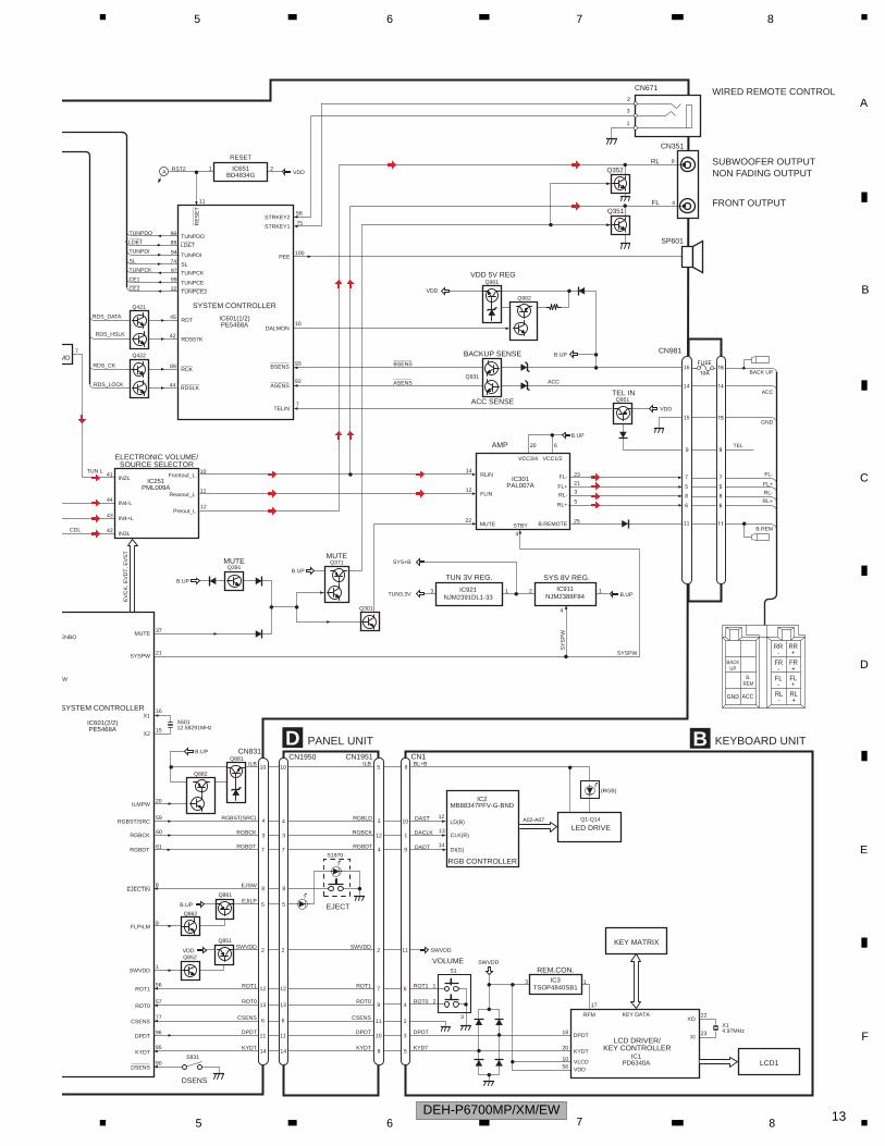
3. BLOCK DIAGRAM AND SCHEMATIC DIAGRAM3.1 BLOCK DIAGRAM
BRST,BRXEN,BSRQ
C
CN901
Q101
M
LASERDIODE
MONITORDIODE
S903DSCSNS
FOCUS ACT.
M1SPINDLEMOTOR
MM2LOADING/CARRIAGE
MOTOR
TRACKING ACT.
LD-
MD
FOPTOP
15
5
14
PICKUP UNIT(P10)(SERVICE)
HOLOGRAM UNIT
IC301BA5835FP
IC201UPD63763GJ
IC703
3V REGULATOR
RF AMP, CD DECODER,MP3 AND WMA DECODER,DIGITAL SERVO/DATA PROCESSOR
CDDRIVER
3VDVD
3VDD
10LOUT
5
CN101
TOP
FOP
16 SOP15 SOM18 LCOP17 LCOM
22
2
LOEJ
31LOUT
9CONT
12 FOP
FD,TD
AC,BD
E,F
SD,MD
3
13 TOP
S901HOME
S90412EJ
S9058EJ
LD+ 14
142 LD
143 PD
CD CORE UNIT(S10.1)
1312
X701
DSCSNS
CONT
LOEJ
HOME
32
97
53
47
VDD
IC203NJM2885DL1-33
3.3V REGULATOR
V3R3D13
VDCONT49
S-812C33AUA-C2N
MICROCOMPUTER
IC701PE5454A
4
V3R3D
19
BDATA,BSCK
VD2
VDD
2
15
5
14
14
VD2
VDCONT
30
31 8EJ
12EJ
X1 X2
reset14 15
RESET
CD3VON46
1CD3VON
75
IC101HA12240FP
TU
CDL
SYSTEM
ICP
CN4011
2,3
CN721
CN101
TUNER AMP UNIT
LOUT
A
TUN3.3V
SYS+B
VDD
ANTENNA
Q101
Q102
Q761
Q762
IC431NJM4558MD
TU
NP
DO
TU
NP
DI
TU
NP
CK
CE
2
LDE
T
CDL
FM/AM TUNER UNIT
IP-BUS
FMRF
ANT adjRF adj
FM ANT
T51 CF52CF51
RFG
ND
OS
CG
ND
DG
ND
AU
DIO
GN
D
NC
VC
C
VD
D_3
.3
3.3V 2.5VIC4
3.3V 2.5V
←
IC22.5V
WC
CE
2
RO
M_V
DD
SL DI
CK
CE
1
LDE
T
DO
RD
S_C
K
RD
S_D
ATA
RD
S_L
OC
K
RD
S_H
SLK
7 6 13 5 10 9 8 11 14 18 19 20 21
1
3
2 12 15 22 16 4 17
IC13.3V
AM ANT FMRFATT
LPFOSC
IC3 EEPROM5.0V
IC55V 3.3V←
ATT
MIXER, IF AMP DET, FM MPX,RDS DECODER
24
23
Rch
Lch
14
A
B.UP
VDD
B.UP
53 4
2
VDCONT
RESET RST2
BUSL+
ASENBO
Q751
BRST,BRXEN,BSRQ,BDATA,BSCK
21
5
19
9
7
BUSL-11
61
5
BUS+
BUS-DOUT
STBY
DIN1
RX
IPPW
TX2
1
8
85
86
ASENBO71
24
5
8
VD2
CD3VON
22
23
20Q753
VD1
DEH-P6700MP/XM/EW121 2 3 4
C
D
F
A
B
E
7
TU
CDL
SYSTEM C
IC6PE
MDR
R
R
W
ENBO
5 6 7 8
11Rearout_L
IN2L
IN4-L
IN4+L
IN3L
41
44
43
IC251PML009A
ELECTRONIC VOLUME/SOURCE SELECTOR
N L
42
10Frontout_L
IC1PD6340A
LCD DRIVER/KEY CONTROLLER
RGB CONTROLLER
KEY DATA
LCD1
11
VDD
B.UP
92
93
37MUTE
21
23
3
5
FL-
FL+
RL-
RL+
ACC
FLIN12
22
AMP
IC601(1/2)PE5468A
ONTROLLER
01(2/2)5468A
IC301PAL007A
VDD
Q901
Q931
VDD
MUTE
CN1CN831
CN1950 CN1951
Q851
Q852
S831
KEYBOARD UNIT
Q301
Q371Q391
B.UP
18
17
13
20
DPDT
RFM
KYDT
SYSTEM CONTROLLER
VDD 5V REG
BACKUP SENSE
ACC SENSE
14
8
6
5
7
16
15
BPANEL UNITD
CN981
TUNPCE
TUNPDO
TUNPDI
99
98
94
TUNPCK97
TUNPDO
TUNPDI
CE1
TUNPCK
Q902
DALMON10
100
2
10
12
13
11
8
14
SWVDD
5
7
9
11
10
8
ILB BL+B
SWVDD
ROT1
ROT0
ROT1
ROT0
DPDT
CSENS
KYDT
DPDT
KYDT
ILB
SWVDD
EJILP
EJSW
ROT1
ROT0
DPDT
CSENS
KYDT
S1970
S1SWVDD1
8
ILMPW20
ROT156
ROT057
DPDT96
KYDT95
RL
CN351
SP601
8
4
SL74SL
RLIN14
SWVDD
EJECTIN
90DSENS
B.UP
Q861
5
FLPILM9
Q862
6
2
10
12
13
11
8
14
5
6CSENS77
BSENS
ASENS
X1
X2
16
X60112.58291MHz15
XO
XI
22
X14.97MHz23
Q352
FLQ351
RESET
4
SYSPW
SY
SP
W
STBY
TUN3.3V
TUN 3V REG.
IC911NJM2388F84 B.UP
SYS 8V REG.
SYS+B
A RST2
B.UP
B.UP
21SYSPW
CN671
1 2
PEE
1125B.REMOTE
RE
SE
T
BSENS
ASENS
2
8
6
4
2
3
5
11
EV
CK
, EV
DT
, EV
ST
32CE2 TUNPCE2
58
75
IC651BD4834G
STRKEY2
STRKEY1
VCC3/4 VCC1/2
B.UP
20 6
IC921NJM2391DL1-33
1213
4
MUTEMUTE
IC3TSOP4840SB1
REM.CON.
1056
VLCDVDD
Q422
Q421
DS_CK
DS_LOCK 44
89
45
42
DS_DATA
RDS_HSLK
3
2
1
RCK
RDSLK
RDT
RDS57K
TELIN7
Q951
VDD
TEL IN
9
1
2
IC2MB88347PFV-G-BND
LD(B)
CLK(R)
DI(G)
A02-A0712
13
14
10
1
9
DAST
DACLK
DADT
Q1-Q14
LED DRIVE
(RGB)
3
12
4
4
3
7
4
3
7
59
60
61
RGBST/SRC
RGBCK
RGBDT
RGBLD
RGBCK
RGBDT
RGBST(SRC)
RGBCK
RGBDT
Preout_L12
3
88LDET LDET
WIRED REMOTE CONTROL
FRONT OUTPUT
SUBWOOFER OUTPUTNON FADING OUTPUT
FL-
FL+
RL-
RL+
BACK UP
GND
RR+
RR-
FR+
FR-
FL+
FL-
RL+
RL-
ACCGND
BACKUP
B.REM
ACC
B.REM
TEL
14
8
6
5
7
16
11
9
15
FUSE
10A
DSENS
EJECT
VOLUME
KEY MATRIX
5
Q881
Q882
DEH-P6700MP/XM/EW 135 6 7 8

C
D
F
A
B
E
sw
vd
d
BEEP
NC
FM(30%)AM(30%
IP-BUSD-DA, MP
1 2 3 4
3.2 OVERALL CONNECTION DIAGRAM(GUIDE PAGE)
CS
A30
-201
N
da
lmo
n
mute
TS
CK
/BS
CK
NC
AS
EN
SB
O
TS
I/BS
I
BC
N1
D PANEL UNIT
CCN901
CD
-DA
, MP
3 : 0
.2dB
14
32
57
6
811
109
IP-B
US
: 2.
2dB
C
EJECT
DSENS
FM
/AM
TU
NE
R U
NIT
FM
(30%
) : -
26dB
AM
(30%
) : -
26dB
A-a A-b
A-a A-b
A-b A-a
Large sizeSCH diagram
Guide page
Detailed page
Note: When ordering service parts, be sure to refer to " EXPLODED VIEWS AND PARTS LIST" or "ELECTRICAL PARTS LIST". A-a
A D
DEH-P6700MP/XM/EW141 2 3 4

C
D
F
A
B
E
da
lmo
nA
SE
NS
BO
A-a A-b
A-a A-b
A-b A-a
5 6 7 8
CEK120810A
>
REARR CH
FRONTR CH
FRONTL CH
REARL CH
>
sw
vd
d
NC
BEEP
NC
A TUNER AMP UNIT
Decimal points for resistorand capacitor fixed valuesare expressed as :2.2 2R20.022 R022
← ←
The > mark found on some component parts indicatesthe importance of the safety factor of the part.Therefore, when replacing, be sure to use parts ofidentical designation.
Symbol indicates a resistor.No differentiation is made between chip resistors anddiscrete resistors.
NOTE :
Symbol indicates a capacitor.No differentiation is made between chip capacitors anddiscrete capacitors.
FM(30%) : -27dBAM(30%) : -27dB
IP-BUS : 2.2dBCD-DA, MP3 : 0.2dB
AM(30%) : -1.9dBFM(30%) : -3.9dB
IP-BUS : 10.3dBCD-DA, MP3 : 10.3dB
FM(30%) : -4.66dBAM(30%) : -2.66dB
IP-BUS : 9.54dBCD-DA, MP3 : 9.54dB
RR+
RR-
FR+
FR-
FL+
FL-
RL+
RL-
ACCGND
BACKUP
B.REM
FM(30%) : 22.1dBAM(30%) : 24.1dB
IP-BUS : 36.3dBCD-DA, MP3 : 36.3dB
A-b
A
DEH-P6700MP/XM/EW 155 6 7 8
C
D
F
A
B
E
mu
te
1 2 3 4
A-a
A-b
A-a
A-a
A-b 1 2 3 dalmon
CC
N90
1
CD-DA, MP3 : 0.2dB
14 3 257 6
811 10 9
IP-BUS : 2.2dB
FM AM I
CD
-D
DEH-P6700MP/XM/EW161 2 3 4

C
D
F
A
B
E
on
5 6 7 8
A-a
A-b
A-a
A-a
A-b
D
4 5 6
CSA30-201N
dalm
mu
te
TSCK/BSCK
NC
ASENSBO
NC
TSI/BSI
BCN1
DP
AN
EL
UN
IT
EJE
CT
DS
EN
S
FM/AM TUNER UNIT FM(30%) : -26dBAM(30%) : -26dB
DEH-P6700MP/XM/EW 175 6 7 8

C
D
F
A
B
E
1 2 3 4
A-a
A-b
A-b 1 2 3
RE
AR
R C
H
FR
ON
TR
CH
FR
ON
TL
CH
RE
AR
L C
H
>
swvdd
dalmon
BE
EP
AT
UN
ER
AM
P U
NIT
FM
(30%
) : -
27dB
AM
(30%
) : -
27dB
IP-B
US
: 2.
2dB
CD
-DA
, MP
3 : 0
.2dB
AM
(30%
) : -
1.9d
BF
M(3
0%)
: -3.
9dB
IP-B
US
: 10
.3dB
CD
-DA
, MP
3 : 1
0.3d
B
FM
(30%
) : -
4.66
dBA
M(3
0%)
: -2.
66dB
IP-B
US
: 9.
54dB
CD
-DA
, MP
3 : 9
.54d
B
DEH-P6700MP/XM/EW181 2 3 4

C
D
F
A
B
E
dd
on
5 6 7 8
A-a
A-b
A-b4 5 6
CE
K12
0810
A
>
swv
dalm
NC
ASENSBO
BE
EP
NC
Dec
imal
poi
nts
for
resi
stor
and
capa
cito
r fix
ed v
alue
sar
e ex
pres
sed
as :
2.2
2R
20.
022
R
022
←
←
The
> m
ark
foun
d on
som
e co
mpo
nent
par
ts in
dica
tes
the
impo
rtan
ce o
f the
saf
ety
fact
or o
f the
par
t.T
here
fore
, whe
n re
plac
ing,
be
sure
to u
se p
arts
of
iden
tical
des
igna
tion.
Sym
bol i
ndic
ates
a r
esis
tor.
No
diffe
rent
iatio
n is
mad
e b
etw
een
chip
res
isto
rs a
nddi
scre
te r
esis
tors
.
NO
TE
: Sym
bol i
ndic
ates
a c
apac
itor.
No
diffe
rent
iatio
n is
mad
e b
etw
een
chip
cap
acito
rs a
nddi
scre
te c
apac
itors
.
RR +
RR -
FR +FR -
FL +FL -
RL +
RL -
AC
CG
ND
BA
CK
UP
B.
RE
M
FM
(30%
) : 2
2.1d
BA
M(3
0%)
: 24.
1dB
IP-B
US
: 36
.3dB
CD
-DA
, MP
3 : 3
6.3d
B
DEH-P6700MP/XM/EW 195 6 7 8

C
D
F
A
B
E
1 2 3 43.3 KEYBOARD UNIT
B
D CN1951
LCD DRIVER/KEY CONTROLLER
RGB CONTROLLER
REM. CON.
FUNCTION
CA
W18
65
DISPLAY
ILLUMINATION
VOLUME
DEH-P6700MP/XM/EW201 2 3 4

C
D
F
A
B
E
5 6 7 8
B B
B KEYBOARD UNIT
: The power supply is shown with the marked box.
DEH-P6700MP/XM/EW 215 6 7 8

C
D
F
A
B
E
TY
1 2 3 4
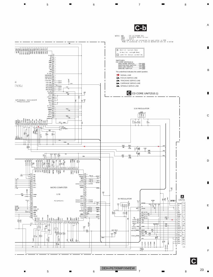
3.4 CD MECHANISM MODULE(GUIDE PAGE)
C-a
C
PICKUP UNIT(P10)(SERVICE)
M1 CXC4440SPINDLE MOTOR
M2 CXB8933LOADING
/CARRIAGE MOTOR CD DRIVER
T
F
F
T
T
T
F
F
FTCS
T
F
S
C
F
F
T
T
S S C C
C
C
S
S
T
T
F
F
1
3
2
0
9 7
$
8
5
4
@
#
%
DEH-P6700MP/XM/EW221 2 3 4
C
D
F
A
B
E
5 6 7 8
C-b
C
ras
SRAMLEVEL0
SRAMLEVEL1
SRAMLEVEL2
TYPE_A/D
SWITCHES:CD CORE UNIT(S10.1) S901:HOME SWITCH..........ON-OFF S903:DSCSNS SWITCH......ON-OFF S904:12EJ SWITCH.............ON-OFF S905:8EJ SWITCH...............ON-OFF
The underlined indicates the switch position.
CD CORE UNIT(S10.1)C
ACN721
FSIGNAL LINE
FOCUS SERVO LINE
TRACKING SERVO LINE
CARRIAGE SERVO LINE
SPINDLE SERVO LINE
T
C
S
3V REGULATOR
3.3V REGULATOR
MICRO COMPUTER
!
^
&
6
DEH-P6700MP/XM/EW 235 6 7 8

C
D
F
A
B
E
1 2 3 4
A-a
C-b
C-a
C-a
C-b 1 2
PIC
KU
P U
NIT
(P10
)(S
ER
VIC
E)
T
F F
T
T TFF
F
T
C
S
T T F F@#
%
DEH-P6700MP/XM/EW241 2 3 4

C
D
F
A
B
E
2
5 6 7 8
A-a
C-b
C-a
C-a
C-b3 4 5 6
M1
CX
C44
40S
PIN
DLE
MO
TO
R
M2
CX
B89
33LO
AD
ING
/CA
RR
IAG
E M
OT
OR
CD
DR
IVE
R
T F
S C
F F T T
S
S
C
C
CCSS
13 2
097$ 8
5
4
DEH-P6700MP/XM/EW 255 6 7 8

C
D
F
A
B
E
1 2 3 4
C-a
C-b
C-b 1 2
ra
s
SW
ITC
HE
S:
CD
CO
RE
UN
IT(S
10.1
)
S90
1:H
OM
E S
WIT
CH
......
....O
N-O
FF
S
903:
DS
CS
NS
SW
ITC
H...
...O
N-O
FF
S
904:
12E
J S
WIT
CH
......
......
.ON
-OF
F
S90
5:8E
J S
WIT
CH
......
......
...O
N-O
FF
The
und
erlin
ed in
dica
tes
the
switc
h po
sitio
n.
CD
CO
RE
UN
IT(S
10.1
)C
FS
IGN
AL
LIN
E
FO
CU
S S
ER
VO
LIN
E
TR
AC
KIN
G S
ER
VO
LIN
E
CA
RR
IAG
E S
ER
VO
LIN
E
SP
IND
LE S
ER
VO
LIN
E
T C S
3.3V
RE
GU
LAT
OR
!
DEH-P6700MP/XM/EW261 2 3 4

C
D
F
A
B
E
2
5 6 7 8
C-a
C-b
C-b3 4 5 6
SR
AM
LEV
EL0
SR
AM
LEV
EL1
SR
AM
LEV
EL2
TY
PE
_A/D
AC
N72
13V
RE
GU
LAT
OR
MIC
RO
CO
MP
UT
ER
^ &
6
DEH-P6700MP/XM/EW 275 6 7 8

C
D
F
A
B
E
1 2 3 4
- Waveforms Note : 1. The encircled numbers denote measuring points in the circuit diagram.2. Reference voltage REFO1(1.65V)
1 DSCSNS2 8SNS3 12SNS4 LOEJ
5V/div5V/div5V/div5V/div
500ms/div
12 cm CD Loading operation
Ref.:GND
Mode:Normal
1 DSCSNS2 8SNS3 12SNS4 LOEJ
5V/div5V/div5V/div5V/div
500ms/div
Ref.:GND
Mode:Normal
1 DSCSNS5 CLCONT4 LOEJ6 VD
5V/div5V/div5V/div10V/div
500ms/div
12 cm CD Loading operation 8 cm CD Loading operation
Ref.:GND
Mode:Normal
0 FIN! RFOK7 SIN
200mV/div2V/div2V/div
500ms/div
12 cm CD-DA Source On setup operation
Ref.:REFO
Mode:Normal
# FE0 FIN@ TE9 TIN
500mV/div500mV/div500mV/div500mV/div
20ms/div
Ref.:REFO
Mode:Normal
@ TE# FE
500mV/div500mV/div
200ms/div
Source On setup operation CD-DA Play operation
Ref.:REFO
Mode:Normal
# FE0 FIN@ TE9 TIN
500mV/div500mV/div500mV/div500mV/div
20ms/div
CD-ROM play operation(Regular track Jump)
Ref.:REFO
Mode:Normal
$ MDX7 SIN
2V/div1V/div
5µs/div
Ref.:REFO
Mode:Normal
$ MDX7 SIN
1V/div200mV/div
50ms/div
Spindle waveform during play operation Spindle waveform during play operation(Wider)
Ref.:REFO
Mode:Normal
7 SIN8 CIN9 TIN
1V/div500mV/div500mV/div
2s/div
12 cm CD-DA setup operation after loading 12 cm CD-ROM(3 sessions) setup operation after loading
Ref.:REFO
Mode:Normal
7 SIN8 CIN9 TIN
1V/div500mV/div500mV/div
2s/div
Ref.:REFO
Mode:Normal
7 SIN8 CIN9 TIN
1V/div500mV/div500mV/div
1s/div
12 cm CD-ROM(1 session) setup operation after loading
Ref.:REFO
Mode:Normal
DEH-P6700MP/XM/EW281 2 3 4

C
D
F
A
B
E
5 6 7 8
0 FIN# FE
500mV/div500mV/div
200ms/div
Focus Search waveform
Ref.:REFO
Mode:TEST
% RFAGC@ TE9 TIN
1V/div500mV/div500mV/div
500µs/div
Ref.:REFO
Mode:TEST
@ TE% RFAGC
500mV/div500mV/div
2ms/div
Track Open waveform 1 Track Jump waveform
Ref.:REFO
Mode:TEST
% RFAGC@ TE8 CIN7 SIN
1V/div1V/div500mV/div2V/div
200ms/div
Ref.:REFO
Mode:Normal
Search operation(Outter to Inner)
^ LOUT& ROUT
1V/div1V/div
200µs/div
Analog audio waveform
Ref.:AGND
Mode:Normal
7 SIN8 CIN9 TIN
1V/div500mV/div500mV/div
500ms/div
Ref.:REFO
Mode:Normal
1 DSCSNS2 8SNS3 12SNS4 LOEJ
5V/div5V/div5V/div5V/div
500ms/div
12 cm CD Eject operation
CD-DA >> CD-ROM mode change(Band key)
Ref.:GND
Mode:Normal
% RFAGC@ TE9 TIN
1V/div500mV/div500mV/div
500µs/div
4 Tracks Jump waveform 32 Tracks Jump waveform
Ref.:REFO
Mode:TEST
% RFAGC@ TE9 TIN
1V/div500mV/div500mV/div
2ms/div
Ref.:REFO
Mode:TEST
% RFAGC@ TE9 TIN
1V/div500mV/div500mV/div
1ms/div
10 Tracks Jump waveform
Ref.:REFO
Mode:TEST
1 DSCSNS5 CLCONT4 LOEJ
5V/div5V/div5V/div
500ms/div
12 cm CD Eject operation
Ref.:GND
Mode:Normal
1 DSCSNS2 8SNS3 12SNS4 LOEJ
5V/div5V/div5V/div5V/div
500ms/div
8 cm CD Eject operation
Ref.:GND
Mode:Normal
DEH-P6700MP/XM/EW 295 6 7 8
C
D
F
A
B
E
1 2 3 4
7 SIN8 CIN9 TIN
1V/div500mV/div500mV/div
500ms/div
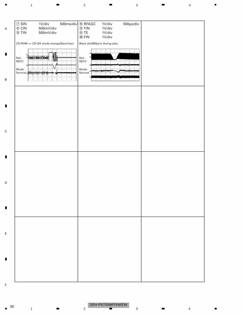
CD-ROM >> CD-DA mode change(Band key)
Ref.:REFO
Mode:Normal
% RFAGC9 TIN@ TE0 FIN
1V/div1V/div1V/div1V/div
500µs/div
Black dot(800µm) during play
Ref.:REFO
Mode:Normal
DEH-P6700MP/XM/EW301 2 3 4

DEH-P6700MP/XM/EW 31
5 6 7 8
5 6 7 8
C
D
F
A
B
E

C
D
F
A
B
E
1 2 3 44. PCB CONNECTION DIAGRAM4.1 TUNER AMP UNIT
CapacitorConnector
P.C.Board Chip Part
A
A TUNER AMP UNIT
SIDE B
SIDE A
NOTE FOR PCB DIAGRAMS1.The parts mounted on this PCB include all necessary parts for several destination. For further information for respective destinations, be sure to check with the schematic dia- gram.2.Viewpoint of PCB diagrams
0 10 20 30 40 50 60 70X
Y
10
20
30
40
50
60
70
80
90
100
110
120
130
140
150
CCN901
IP-BUS
WIRED REMOTE CONTROLCORD ASSY
1
2
3
1234
891011
567
13579111315
246810121416
DSENS
DEH-P6700MP/XM/EW321 2 3 4
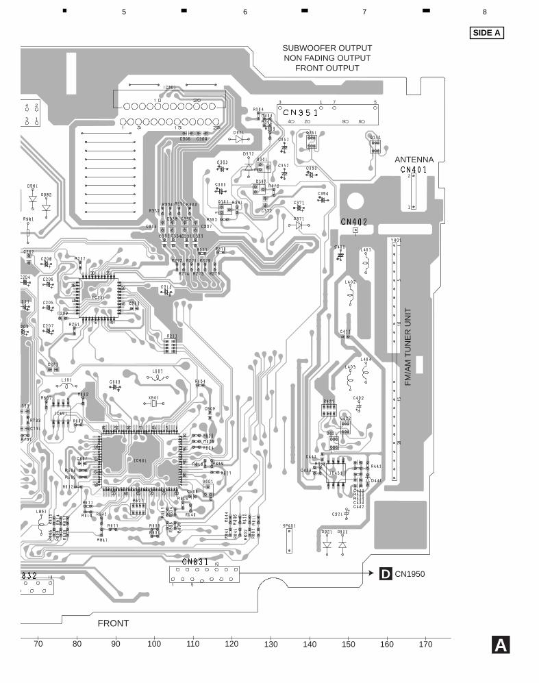
5 6 7 8
SIDE A
70
13
24
A80 90 100 110 120 130 140 150 160 170
4 2
13
8 6
57
D CN1950
FRONT
ANTENNA
FM
/AM
TU
NE
R U
NIT
SUBWOOFER OUTPUTNON FADING OUTPUT
FRONT OUTPUT
2
1

C
D
F
A
B
E
1 2 3 4
A
A TUNER AMP UNIT
90100110120130140150160170
1
DEH-P6700MP/XM/EW341 2 3 4

C
D
F
A
B
E
9
5 6 7 8
A
SIDE B
010203040506070800 X
Y
10
20
30
40
50
60
70
80
90
100
110
120
130
140
150
1
1
DEH-P6700MP/XM/EW 355 6 7 8
C
D
F
A
B
E
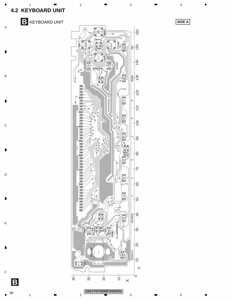
1 2 3 44.2 KEYBOARD UNIT
B
B KEYBOARD UNIT SIDE A
0
10203040
1020
3040
5060
7080
9010
011
012
013
014
015
016
0
X
Y
TA
VO
LUM
E
DIS
PLA
YS
OU
RC
E1
23
45
6B
AN
DS
W
AU
DIO
FU
NC
TIO
N
DO
WN
UP
RIG
HT
LEF
T
ILLU
MIN
AT
ION
EQ
DEH-P6700MP/XM/EW361 2 3 4
C
D
F
A
B
E
5 6 7 8
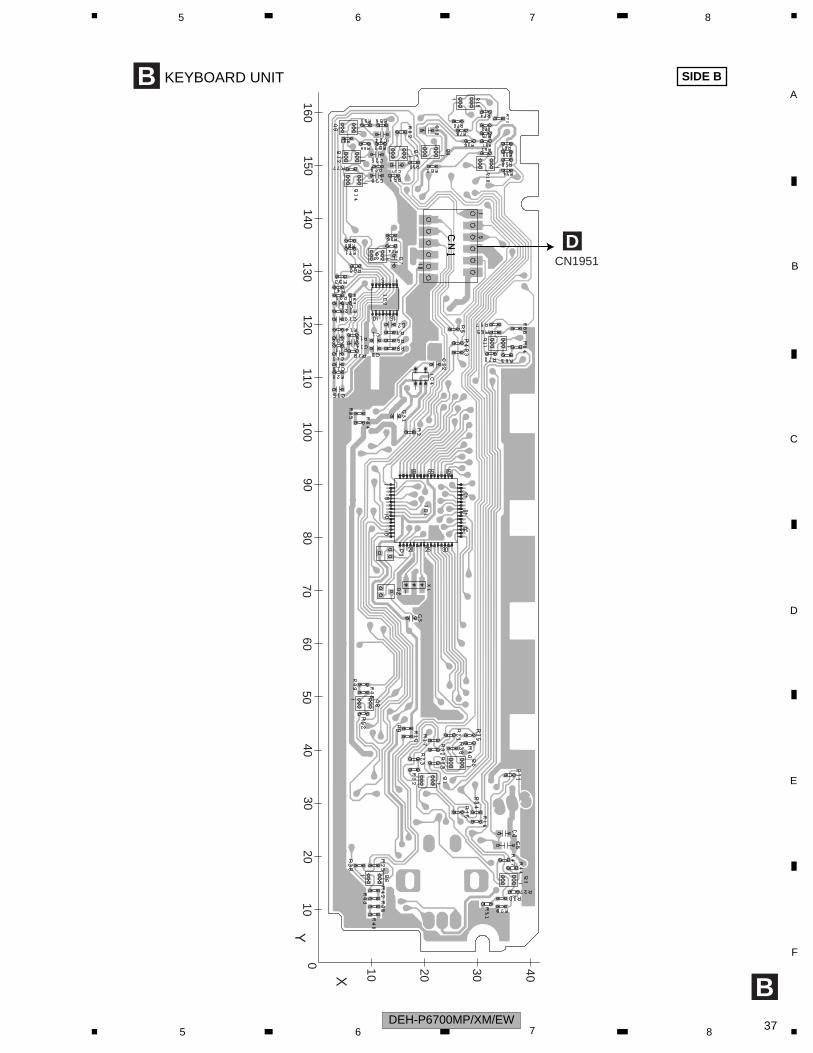
B
B KEYBOARD UNIT SIDE B
0 10 20 30 40
160150
140130
120110
10090
8070
6050
4030
2010
X
Y
DCN1951
DEH-P6700MP/XM/EW 375 6 7 8

C
D
F
A
B
E
1 2 3 4
4.3 CD CORE UNIT(S10.1)
C
C CD CORE UNIT(S10.1) SIDE A
ACN721
PIC
KU
P U
NIT
(P10
)(S
ER
VIC
E)
HOME
M2LOADING
/CARRIAGEMOTOR
M1SPINDLEMOTOR
EF
REFO1
DEH-P6700MP/XM/EW381 2 3 4

C
D
F
A
B
E
5 6 7 8
C
C CD CORE UNIT(S10.1) SIDE B
12EJ8EJ
DSCSNS
DEH-P6700MP/XM/EW 395 6 7 8
C
D
F
A
B
E
1 2 3 4
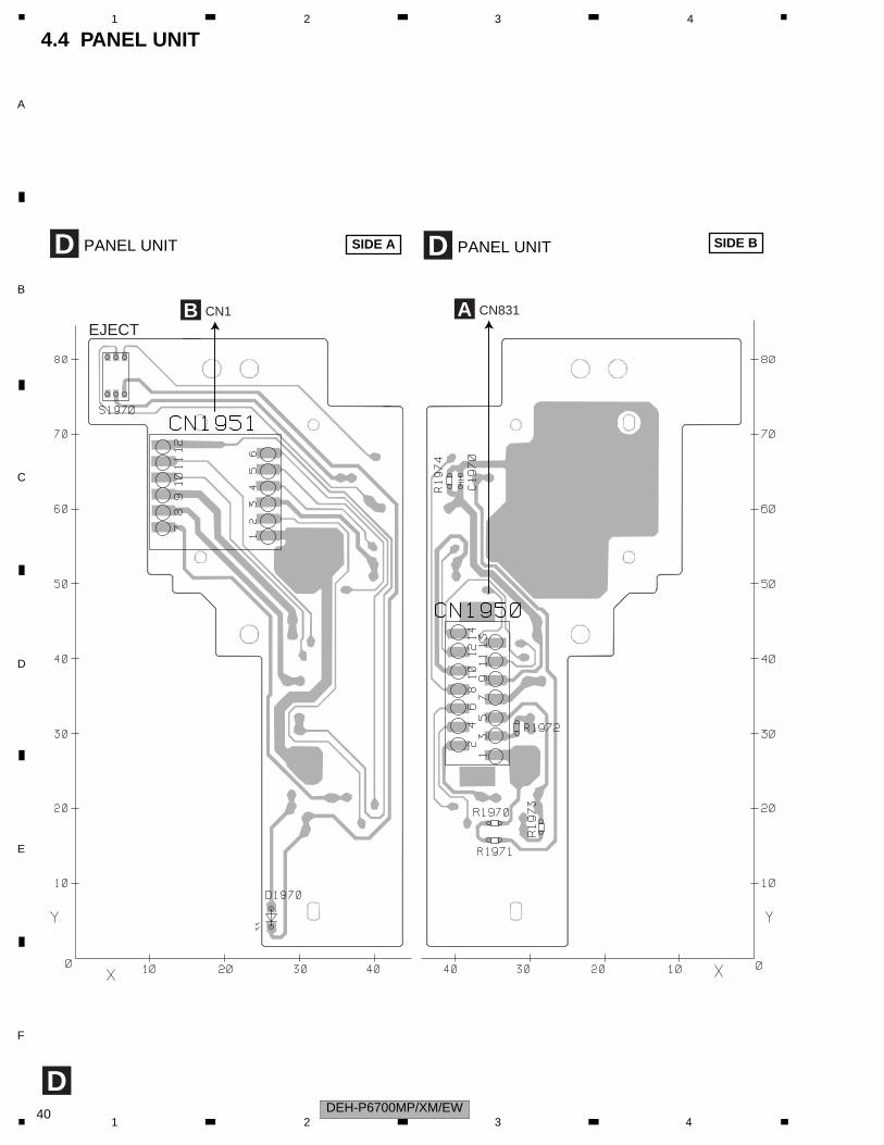
4.4 PANEL UNIT
D
D PANEL UNIT D PANEL UNITSIDE A SIDE B
B CN1
EJECTA CN831
DEH-P6700MP/XM/EW401 2 3 4

C
D
F
A
B
E
5 6 7 8
5. ELECTRICAL PARTS LIST
NOTE:• Parts whose parts numbers are omitted are subject to being not supplied.• The part numbers shown below indicate chip components. Chip Resistor RS1/_S___J,RS1/__S___J Chip Capacitor (except for CQS.....) CKS....., CCS....., CSZS.....• The > mark found on some component parts indicatesthe importance of the safety factor of the part. Therefore, when replacing, be sure to use parts of identical designation. • Meaning of the figures and others in the parentheses in the parts list. Example) IC 301 is on the point (face A, 91 of x-axis, and 111 of y-axis) of the corresponding PC board. IC 301 (A, 91, 111) IC NJM2068V
Circuit Symbol and No. Part No.
DEH-P6700MP/XM/EWTuner Amp Unit : CWM9790Keyboard Unit : NSPPanel Unit : CWM9781CD Core Unit(S10.1) : CWX3096
AUnit Number:CWM9790Unit Name:Tuner Amp Unit
MISCELLANEOUS
IC 101 (A,58,64) IC HA12240FPIC 251 (A,86,88) IC PML009AIC 301 (A,104,139) IC PAL007AIC 431 (A,147,43) IC NJM4558MDIC 601 (A,96,46) IC PE5468A
IC 651 (A,54,73) IC BD4834GIC 911 (A,5,120) IC NJM2388F84IC 921 (B,159,27) IC NJM2391DL1-33Q 101 (A,45,85) Transistor 2SA1576Q 102 (A,46,82) Transistor DTC124EU
Q 301 (A,128,122) Transistor DTC124EUQ 351 (A,141,128) Transistor UMH3NQ 352 (A,157,127) Transistor UMH3NQ 371 (B,137,115) Transistor UMD2NQ 391 (A,118,111) Transistor 2SC4081
Q 421 (A,146,50) Transistor UMH1NQ 422 (A,149,54) Transistor UMH1NQ 751 (A,6,70) Transistor 2SD2396Q 753 (B,26,55) Transistor UMD2NQ 761 (B,28,33) Transistor 2SA1577
Q 762 (B,22,33) Transistor DTC114EUQ 851 (B,65,35) Transistor 2SA1576Q 852 (B,63,30) Transistor DTC114EUQ 861 (A,45,16) Transistor 2SA1576Q 862 (A,41,16) Transistor DTC114EU
Q 881 (B,41,16) Transistor 2SD2318F5Q 882 (A,27,17) Transistor UMD3NQ 901 (A,6,104) Transistor 2SD2396
Q 902 (B,31,69) Transistor UMD2NQ 931 (A,60,117) Transistor UMX1N
Q 951 (A,56,106) Transistor 2SA1576D 391 (A,17,86) Diode HZS7L(B2)D 392 (A,127,116) Diode DAN202UD 441 (A,155,41) Diode UDZS5R6(B)D 751 (A,16,65) Diode HZS9L(A1)
D 801 (B,120,29) Diode UMZ6R8END 802 (B,108,29) Diode UMZ6R8END 803 (B,66,27) Diode UDZS10(B)D 881 (A,31,15) Diode HZS9L(B1)D 882 (A,28,25) Diode MPG06G-6415G50
D 901 (A,29,79) Diode HZS6L(B1)D 902 (A,32,75) Diode MPG06G-6415G50D 921 (A,145,24) Diode MPG06G-6415G50D 931 (A,54,115) Diode HZU7L(C3)D 932 (A,60,113) Diode HZU7L(A1)
D 951 (A,60,108) Diode DAN202UD 971 (A,122,129) Diode MPG06G-6415G50D 972 (A,124,122) Diode MPG06G-6415G50D 981 (A,69,113) Diode MPG06G-6415G50D 982 (A,72,111) Diode MPG06G-6415G50
ZNR401 (B,158,113) Surge Protector CSA30-201NL 101 (A,77,65) Inductor LAU2R2KL 211 (A,60,87) Inductor LAU2R2KL 401 (A,155,97) Ferri-Inductor LAU4R7KL 402 (A,151,89) Inductor LAU1R0K
L 403 (A,151,67) Inductor LAU1R0KL 601 (A,101,67) Inductor LAU2R2KL 701 (A,51,54) Inductor LAU2R2KL 851 (A,71,29) Inductor LAU2R2KL 951 (A,64,104) Inductor LAU2R2K
L 981 (A,32,107) Choke Coil 600µH CTH1291X 601 (A,100,61) Radiator 12.58291MHz CSS1402S 831 (A,25,10) Switch(DSENS) CSN1039>FU351 (B,127,134) Fuse 3A CEK1286SP601 (A,135,25) Buzzer CPV1062
Y 401 (A,162,101) FM/AM Tuner Unit CWE1645> Fuse 10A CEK1208
RESISTORS
Circuit Symbol and No. Part No.
DEH-P6700MP/XM/EW 415 6 7 8

C
D
F
A
B
E
1 2 3 4
R 101 (B,36,134) RS1/16S150JR 102 (B,36,135) RS1/16S470JR 103 (B,37,124) RS1/16S101JR 104 (B,36,137) RS1/16S101JR 105 (B,27,135) RS1/16S181J
R 106 (B,31,121) RS1/16S181JR 107 (B,25,135) RS1/16S223JR 108 (B,29,121) RS1/16S223JR 109 (B,26,122) RS1/16S102JR 110 (B,27,121) RS1/16S102J
R 111 (B,34,121) RS1/16S222JR 113 (A,42,83) RS1/16S332JR 114 (A,43,80) RS1/16S562JR 211 (A,104,75) RAB4C102JR 251 (A,79,79) RS1/16S102J
R 252 (A,81,96) RS1/16S102JR 271 (A,110,96) RS1/16S101JR 272 (A,106,96) RS1/16S101JR 273 (A,111,96) RS1/16S101JR 274 (A,108,96) RS1/16S101J
R 275 (A,113,96) RS1/16S101JR 276 (A,116,96) RS1/16S101JR 301 (B,118,125) RS1/16S153JR 302 (A,129,132) RS1/16S103JR 303 (A,129,134) RS1/16S103J
R 304 (A,127,135) RS1/16S331JR 331 (A,106,110) RSK1/16S471JR 332 (A,102,110) RSK1/16S471JR 333 (A,109,110) RSK1/16S471JR 334 (A,104,110) RSK1/16S471J
R 351 (B,131,127) RS1/16S821JR 352 (B,141,129) RS1/16S821JR 353 (B,141,123) RS1/16S821JR 354 (B,158,127) RS1/16S821JR 355 (B,129,130) RS1/16S223J
R 356 (B,140,129) RS1/16S223JR 357 (B,143,123) RS1/16S223JR 368 (B,156,126) RS1/16S223JR 371 (B,142,109) RS1/16S102JR 372 (A,131,115) RS1/16S0R0J
R 391 (A,121,111) RS1/16S104JR 392 (A,118,108) RS1/16S104JR 393 (A,130,130) RS1/16S222JR 401 (B,158,64) RS1/16S681JR 402 (B,157,81) RS1/16S681J
R 403 (B,157,83) RS1/16S681JR 404 (B,157,86) RS1/16S681JR 405 (B,157,88) RS1/16S681JR 407 (B,157,90) RS1/16S681JR 408 (B,158,69) RS1/16S0R0J
R 421 (A,145,59) RAB4C223JR 422 (B,157,79) RS1/16S681JR 431 (B,153,43) RS1/16S103JR 432 (B,153,41) RS1/16S103JR 433 (A,153,44) RS1/16S103J
R 434 (A,153,42) RS1/16S103JR 435 (B,154,47) RS1/16S103JR 436 (B,152,45) RS1/16S103JR 437 (B,146,47) RS1/16S103JR 438 (A,143,43) RS1/16S103J
Circuit Symbol and No. Part No.
R 441 (A,155,45) RS1/16S681JR 601 (B,134,38) RS1/16S102JR 603 (B,97,54) RS1/16S104JR 604 (A,112,65) RS1/16S104JR 605 (B,102,57) RS1/16S102J
R 606 (B,91,53) RS1/16S473JR 607 (A,72,60) RS1/16S104JR 610 (A,83,33) RS1/16S103JR 611 (A,83,34) RS1/16S473JR 612 (A,80,39) RS1/16S104J
R 613 (A,103,33) RS1/16S103JR 616 (B,115,45) RS1/16S472JR 617 (A,116,43) RS1/16S102JR 620 (B,107,44) RS1/16S104JR 621 (B,119,45) RS1/16S104J
R 622 (B,121,45) RS1/16S104JR 623 (B,124,45) RS1/16S104JR 624 (A,111,49) RS1/16S681JR 625 (A,111,51) RS1/16S681JR 626 (A,111,52) RS1/16S681J
R 627 (A,96,33) RAB4C471JR 640 (A,109,34) RS1/16S0R0JR 651 (A,60,72) RS1/16S183JR 652 (A,59,73) RS1/16S102JR 671 (B,7,134) RS1/16S102J
R 672 (B,5,134) RS1/16S102JR 701 (A,61,44) RS1/16S221JR 702 (A,61,35) RS1/16S221JR 703 (A,61,36) RS1/16S102JR 704 (A,61,47) RS1/16S102J
R 705 (A,61,46) RS1/16S221JR 706 (A,61,38) RS1/16S221JR 707 (A,44,45) RS1/16S221JR 708 (A,61,41) RAB4C682JR 712 (B,49,51) RS1/16S473J
R 731 (A,67,52) RS1/16S6800DR 732 (A,58,54) RS1/16S6800DR 733 (A,67,56) RS1/16S0R0JR 734 (A,61,56) RS1/16S0R0JR 751 (A,16,57) RD1/4PU102J
R 761 (B,30,36) RS1/16S103JR 762 (B,25,30) RS1/16S152JR 801 (A,127,27) RS1/16S222JR 802 (A,125,27) RS1/16S222JR 803 (A,78,27) RS1/16S222J
R 804 (A,76,27) RS1/16S222JR 805 (A,74,27) RS1/16S222JR 835 (A,105,29) RS1/16S222JR 836 (A,100,26) RS1/16S104JR 838 (A,103,29) RS1/16S222J
R 839 (A,100,28) RS1/16S104JR 841 (A,86,27) RS1/16S222JR 843 (A,120,27) RS1/16S222JR 845 (A,122,27) RS1/16S222JR 851 (B,61,34) RS1/16S473J
R 852 (B,60,31) RS1/16S472JR 853 (B,60,26) RS1/16S222JR 861 (A,49,16) RD1/4PU391JR 862 (A,45,12) RS1/16S473JR 863 (A,41,12) RS1/16S103J
Circuit Symbol and No. Part No.
DEH-P6700MP/XM/EW421 2 3 4

C
D
F
A
B
E
5 6 7 8
R 881 (A,26,20) RD1/4PU222JR 882 (B,18,27) RS1/16S222JR 901 (B,11,77) RS1/16S333JR 902 (B,14,75) RS1/16S103JR 911 (B,6,110) RS1/16S103J
R 912 (A,16,98) RS1/16S102JR 931 (A,57,115) RS1/16S104JR 932 (A,56,115) RS1/16S473JR 933 (A,64,115) RS1/16S103JR 934 (A,64,112) RS1/16S473J
R 935 (A,62,115) RS1/16S472JR 951 (A,54,103) RS1/16S102JR 952 (A,53,107) RS1/16S472JR 953 (A,57,109) RS1/16S472JR 954 (A,58,103) RS1/16S153J
R 981 (A,67,105) RD1/4PU102J
CAPACITORS
C 101 (B,29,137) CKSRYB104K25C 103 (A,59,69) CKSRYB102K50C 104 (A,61,69) CKSRYB102K50C 105 (B,38,127) CCSRCH101J50C 106 (B,31,137) CCSRCH101J50
C 107 (A,51,64) CKSRYB472K50C 108 (B,45,65) CCSRCH680J50C 201 (B,121,79) CKSRYB105K10C 202 (B,121,75) CKSRYB105K10C 203 (A,66,79) 1µF/50V CCH1510
C 204 (A,67,92) 1µF/50V CCH1510C 205 (A,73,85) CEJQ2R2M50C 206 (A,73,91) CEJQ2R2M50C 207 (A,73,79) CEJQ2R2M50C 208 (A,72,97) CEJQ2R2M50
C 211 (A,66,86) 47µF/10V CCH1558C 212 (B,72,89) CKSRYB104K25C 213 (A,103,89) CEJQ100M16C 251 (A,76,74) CEJQNP4R7M16C 252 (A,81,100) CEJQNP4R7M16
C 253 (A,82,74) CEJQNP4R7M16C 254 (A,87,100) CEJQNP4R7M16C 255 (A,89,74) CEJQNP4R7M16C 256 (A,95,100) CEJQNP4R7M16C 257 (A,95,73) CEJQNP4R7M16
C 258 (A,99,95) CEJQNP4R7M16C 259 (A,76,83) CKSRYB474K10C 261 (A,74,69) CCSQCH152J50C 262 (A,68,98) CCSQCH152J50C 301 (A,48,124) 3300µF/16V CCH1486
C 302 (B,105,144) CKSQYB105K16C 303 (A,118,121) CEHAR100M16C 304 (A,112,130) CKSQYB225K10C 305 (A,117,115) CEHAR330M10C 306 (A,109,130) CKSQYB225K10
C 331 (A,108,102) CKSRYB474K10C 332 (A,103,102) CKSRYB474K10C 333 (A,111,102) CKSRYB474K10C 334 (A,105,102) CKSRYB474K10C 335 (A,108,106) CKSQYB474K16
Circuit Symbol and No. Part No.C 336 (A,102,106) CKSQYB474K16C 337 (A,111,106) CKSQYB474K16C 338 (A,105,106) CKSQYB474K16C 351 (A,134,127) CEJQ100M16C 352 (A,134,120) CEJQ100M16
C 353 (A,141,120) CEJQ100M16C 354 (A,144,113) CEJQ100M16C 361 (B,160,139) CKSRYB104K25C 401 (B,165,59) CKSRYB103K50C 402 (A,153,60) CEJQ470M6R3
C 403 (B,165,64) CKSRYB103K50C 404 (B,165,96) CKSRYB103K50C 405 (A,148,99) CEJQ101M16C 407 (B,158,60) CKSYB475K10C 411 (A,149,78) CCSRCH101J50
C 412 (B,140,65) CCSRCH101J50C 431 (B,156,43) CKSRYB474K10C 432 (B,156,41) CKSRYB474K10C 433 (A,153,45) CCSRCH470J50C 434 (A,153,41) CCSRCH470J50
C 435 (B,157,47) CKSRYB474K10C 436 (B,156,45) CKSRYB474K10C 437 (B,146,46) CCSRCH470J50C 438 (A,141,43) CCSRCH470J50C 441 (A,143,47) CKSRYB105K10
C 442 (A,153,39) CKSRYB105K10C 602 (B,92,67) CKSRYB105K10C 603 (A,90,65) CEJQ4R7M35C 604 (B,101,58) CCSRCH200J50C 605 (B,97,58) CCSRCH200J50
C 606 (B,91,55) CKSRYB105K10C 607 (A,81,45) CKSRYB104K25C 609 (A,114,58) CCSRCH470J50C 611 (B,85,52) CCSRCH680J50C 651 (A,64,72) CKSRYB105K10
C 712 (B,38,30) CCSRCH101J50C 731 (A,66,54) CCSQCH222J50C 732 (A,62,54) CCSQCH222J50C 751 (B,21,63) CKSRYB224K10C 752 (B,15,54) CKSRYB102K50
C 753 (A,15,51) CEJQ101M16C 761 (B,28,41) CKSRYB473K50C 762 (A,29,44) CEAT471M16C 801 (B,87,22) CCSRCH220J50C 802 (B,89,22) CCSRCH220J50
C 803 (B,91,22) CCSRCH220J50C 804 (B,93,22) CCSRCH220J50C 805 (B,114,31) CCSRCH220J50C 881 (B,28,17) CKSRYB104K25C 882 (A,17,31) CEJQ1R0M50
C 901 (A,16,70) CEJQ221M6R3C 902 (B,21,68) CKSRYB103K50C 903 (B,34,81) CKSRYB472K50C 904 (A,25,70) 470µF/16V CCH1331C 911 (A,17,80) CEJQ221M10
C 912 (B,9,116) CKSRYB103K50C 913 (A,14,118) CEJQ101M16C 921 (A,150,32) CEJQ220M10C 922 (B,155,32) CKSRYB103K50C 923 (B,152,21) CKSYB475K10
Circuit Symbol and No. Part No.
DEH-P6700MP/XM/EW 435 6 7 8

C
D
F
A
B
E
1 2 3 4
C 931 (A,62,112) CKSRYB104K25C 981 (B,58,122) CKSRYB104K25
BUnit Number:Unit Name:Keyboard Unit
MISCELLANEOUS
IC 1 (B,85,20) IC PD6340AIC 2 (B,125,13) IC MB88347PFV-G-BNDIC 3 (A,30,37) IC TSOP4840SB1Q 1 (B,34,21) Transistor UMX1NQ 2 (B,133,11) Transistor UMX1N
Q 3 (B,16,36) Transistor UMX1NQ 4 (B,153,21) Transistor UMX1NQ 5 (B,38,26) Transistor UMX1NQ 6 (B,16,11) Transistor UMX1NQ 7 (B,152,15) Transistor UMX1N
Q 8 (B,49,9) Transistor UMX1NQ 9 (B,157,6) Transistor UMX1NQ 10 (B,150,32) Transistor UMX1NQ 11 (B,117,34) Transistor UMX1NQ 12 (B,152,6) Transistor UMX1N
Q 13 (B,162,28) Transistor UMX1NQ 14 (B,147,7) Transistor UMX1ND 1 (B,77,13) Diode DAN202UD 2 (B,70,13) Diode DAP202UD 3 (A,30,23) Chip LED NSCM315CT
D 4 (A,39,22) Chip LED NSCM315CTD 5 (A,84,5) Chip LED NSCM315CTD 6 (A,129,22) Chip LED NSCM315CTD 7 (A,152,23) Chip LED NSCM315CTX 1 (B,71,18) Ceramic Resonator 4.97MHz CSS1573
S 1 (A,15,23) Encoder(VOLUME) XSD7001S 2 (A,38,7) Push Switch CSG1173S 3 (A,52,7) Push Switch CSG1173S 4 (A,64,7) Push Switch CSG1173S 5 (A,76,7) Push Switch CSG1173
S 6 (A,103,7) Push Switch CSG1173S 7 (A,91,7) Push Switch CSG1173S 8 (A,115,7) Push Switch CSG1173S 9 (A,130,7) Push Switch CSG1173S 10 (A,138,30) Push Switch CSG1173
S 11 (A,150,7) Push Switch CSG1173S 12 (A,138,17) Push Switch CSG1173S 13 (A,152,15) Switch CSG1110S 14 (A,152,32) Switch CSG1110S 15 (A,143,23) Switch CSG1110
S 16 (A,160,23) Switch CSG1110S 17 (A,29,30) Push Switch CSG1173S 18 (A,13,8) Push Switch CSG1173S 19 (A,8,36) Push Switch CSG1173S 20 (A,29,17) Push Switch CSG1173
LCD1 (A,84,24) LCD CAW1865
RESISTORS
R 2 (B,100,17) RS1/16S103JR 3 (B,115,26) RS1/16S222JR 4 (B,117,26) RS1/16S222J
Circuit Symbol and No. Part No.R 5 (B,119,26) RS1/16S104JR 6 (B,117,14) RS1/16S102J
R 7 (B,119,14) RS1/16S102JR 8 (B,116,14) RS1/16S102JR 10 (B,43,17) RS1/16S121JR 11 (B,35,36) RS1/16S2R2JR 12 (B,123,4) RS1/16S104J
R 13 (B,116,4) RS1/16S104JR 14 (B,119,4) RS1/16S104JR 15 (B,28,26) RS1/16S121JR 16 (B,27,30) RS1/16S121JR 17 (B,42,22) RS1/16S101J
R 18 (B,115,7) RS1/16S104JR 19 (B,118,7) RS1/16S104JR 21 (B,43,25) RS1/16S101JR 22 (B,36,18) RS1/16S680JR 23 (B,38,18) RS1/16S680J
R 24 (B,135,14) RS1/16S104JR 25 (B,18,11) RS1/16S101JR 26 (B,137,14) RS1/16S222JR 27 (B,13,37) RS1/16S101JR 28 (B,11,35) RS1/16S101J
R 29 (B,126,4) RS1/16S102JR 30 (B,12,35) RS1/16S101JR 31 (B,11,32) RS1/16S101JR 32 (B,40,22) RS1/16S101JR 33 (B,38,22) RS1/16S121J
R 34 (B,28,30) RS1/16S121JR 35 (B,43,29) RS1/16S101JR 36 (B,155,29) RS1/16S104JR 37 (B,155,32) RS1/16S222JR 38 (B,18,8) RS1/16S101J
R 39 (B,40,25) RS1/16S680JR 40 (B,41,29) RS1/16S680JR 41 (B,127,4) RS1/16S102JR 42 (B,14,11) RS1/16S121JR 43 (B,12,11) RS1/16S121J
R 44 (B,18,37) RS1/16S101JR 45 (B,11,11) RS1/16S680JR 46 (B,9,11) RS1/16S680JR 47 (B,19,35) RS1/16S101JR 48 (B,51,9) RS1/16S101J
R 49 (B,52,9) RS1/16S101JR 50 (B,151,18) RS1/16S104JR 51 (B,148,14) RS1/16S222JR 52 (B,47,9) RS1/16S101JR 53 (B,129,4) RS1/16S102J
R 54 (B,149,36) RS1/16S101JR 55 (B,158,9) RS1/16S104JR 56 (B,158,12) RS1/16S222JR 57 (B,120,33) RS1/16S101JR 58 (B,151,36) RS1/16S121J
R 59 (B,153,36) RS1/16S121JR 60 (B,131,7) RS1/16S102JR 61 (B,152,32) RS1/16S680JR 62 (B,150,22) RS1/16S680JR 63 (B,114,36) RS1/16S121J
R 64 (B,116,37) RS1/16S121JR 65 (B,119,33) RS1/16S680JR 66 (B,119,37) RS1/16S680J
Circuit Symbol and No. Part No.
DEH-P6700MP/XM/EW441 2 3 4

C
D
F
A
B
E
5 6 7 8
R 67 (B,154,36) RS1/16S101JR 68 (B,154,9) RS1/16S104J
R 69 (B,154,12) RS1/16S222JR 70 (B,115,33) RS1/16S101JR 71 (B,134,6) RS1/16S102JR 72 (B,159,34) RS1/16S101JR 73 (B,158,32) RS1/16S101J
R 74 (B,160,32) RS1/16S101JR 75 (B,156,32) RS1/16S101JR 76 (B,158,26) RS1/16S101JR 77 (B,149,6) RS1/16S104JR 78 (B,157,27) RS1/16S101J
R 79 (B,150,11) RS1/16S222JR 80 (B,136,6) RS1/16S102JR 81 (B,155,6) RS1/16S0R0JR 82 (B,156,16) RS1/16S0R0JR 83 (B,125,6) RS1/16S0R0J
R 84 (B,102,8) RS1/16S471JR 85 (B,103,8) RS1/16S471J
CAPACITORS
C 4 (B,24,35) CKSQYB475K6R3C 5 (B,65,18) CKSRYB105K10C 7 (B,132,14) CKSQYB225K10C 8 (A,28,14) CKSRYF104Z25C 9 (A,29,19) CKSRYF104Z25
C 10 (B,121,4) CKSRYB103K50C 11 (B,115,4) CKSRYB103K50C 12 (B,118,4) CKSRYB103K50C 13 (B,113,4) CKSRYB103K50C 14 (B,117,7) CKSRYB103K50
C 16 (B,157,21) CKSQYB225K10C 18 (B,124,4) CKSRYB104K25C 19 (A,30,28) CKSRYF104Z25C 20 (A,30,26) CKSRYF104Z25C 21 (B,150,15) CKSQYB225K10
C 22 (A,79,6) CKSRYF104Z25C 23 (A,81,6) CKSRYF104Z25C 24 (B,156,12) CKSQYB225K10C 25 (A,136,25) CKSRYF104Z25C 26 (B,152,11) CKSQYB225K10
C 27 (A,136,22) CKSRYF104Z25C 28 (B,148,11) CKSQYB225K10C 29 (A,155,24) CKSRYF104Z25C 30 (A,149,23) CKSRYF104Z25
DUnit Number:CWM9781Unit Name:Panel Unit
MISCELLANEOUS
D 1970 (A,26,5) LED CL220PGCS 1970 (A,5,78) Push Switch(EJECT) CSG1174
RESISTORS
R 1970 (B,35,18) RS1/16S101JR 1971 (B,35,16) RS1/16S101J
Circuit Symbol and No. Part No.CAPACITORS
C 1970 (B,39,64) CKSRYB104K16
CUnit Number:CWX3096Unit Name:CD Core Unit(S10.1)
MISCELLANEOUS
IC 201 (A,39,24) IC UPD63763GJIC 203 (B,45,78) IC NJM2885DL1-33IC 301 (A,49,88) IC BA5835FPIC 701 (A,48,51) IC PE5454AIC 703 (A,30,44) IC S-812C33AUA-C2N
Q 101 (A,20,22) Transistor 2SA1577Q 701 (B,62,59) Transistor UN2111L 203 (A,53,32) Inductor CTF1389L 207 (A,53,31) Inductor CTF1389L 209 (A,26,20) Inductor CTF1389
L 703 (A,64,49) Inductor CTF1389X 201 (A,51,35) Ceramic Resonator 16.934MHz CSS1603X 701 (A,59,53) Ceramic Resonator 4.00MHz CSS1652S 901 (A,15,43) Switch(HOME) CSN1067S 903 (B,53,100) Switch(DSCSNS) CSN1068
S 904 (B,35,108) Switch(12EJ) CSN1067S 905 (B,48,109) Switch(8EJ) CSN1067
RESISTORS
R 101 (A,22,24) RS1/10SR2R4JR 102 (A,22,26) RS1/10SR2R4JR 103 (A,25,25) RS1/10SR2R7JR 201 (A,53,16) RS1/16SS102JR 202 (A,55,21) RS1/16SS333J
R 221 (B,31,18) RS1/16SS103JR 222 (B,26,18) RS1/16SS103JR 225 (A,27,8) RS1/16SS103JR 226 (A,27,7) RS1/16SS393JR 227 (B,33,10) RS1/16SS562J
R 228 (B,36,8) RS1/16SS122JR 229 (B,34,8) RS1/16SS472JR 232 (B,35,10) RS1/16SS122JR 241 (B,42,28) RS1/16SS333JR 243 (B,44,28) RS1/16SS333J
R 245 (A,39,38) RS1/16SS333JR 301 (A,48,78) RS1/16SS183JR 302 (A,42,78) RS1/16SS822JR 304 (A,50,78) RS1/16SS183JR 305 (A,42,77) RS1/16SS822J
R 307 (A,36,85) RS1/16SS183JR 308 (A,32,83) RS1/16SS183JR 309 (A,38,89) RS1/16SS183JR 310 (A,35,88) RS1/16SS183JR 601 (B,43,59) RS1/16S101J
R 602 (B,41,62) RS1/16S101JR 606 (B,44,67) RS1/16S0R0JR 607 (B,43,56) RS1/16SS0R0JR 608 (B,36,67) RS1/16SS0R0JR 705 (B,50,59) RS1/16SS221J
Circuit Symbol and No. Part No.
DEH-P6700MP/XM/EW 455 6 7 8

C
D
F
A
B
E
1 2 3 4
R 706 (B,57,61) RS1/16SS221JR 707 (A,62,47) RS1/16SS473JR 708 (B,50,57) RS1/16SS221JR 710 (A,28,77) RS1/16SS102JR 711 (B,44,53) RS1/16SS221J
R 714 (B,51,53) RS1/16SS473JR 716 (A,63,56) RS1/16SS472JR 719 (B,49,45) RS1/16SS221JR 720 (B,46,52) RS1/16SS471JR 724 (A,62,42) RS1/16S473J
R 725 (B,57,43) RS1/16SS222JR 726 (A,52,41) RS1/16SS103JR 727 (B,50,54) RS1/16SS473JR 729 (A,57,40) RS1/16SS223JR 730 (A,65,41) RS1/16SS473J
R 731 (A,53,41) RS1/16SS104JR 737 (A,41,42) RS1/16SS104JR 740 (A,35,46) RS1/16SS473JR 742 (A,50,41) RS1/16SS104JR 746 (B,60,56) RS1/16SS104J
R 750 (A,39,59) RS1/16SS473JR 754 (B,48,60) RS1/16SS102JR 755 (A,43,61) RS1/16SS102JR 765 (B,51,40) RAB4CQ221JR 769 (B,48,40) RAB4CQ221J
R 773 (B,39,37) RAB4CQ221JR 777 (B,48,51) RS1/16SS221JR 778 (B,48,52) RS1/16SS221JR 779 (B,45,54) RS1/16SS221JR 901 (B,52,65) RAB4CQ221J
R 905 (B,54,60) RS1/16SS221JR 906 (B,56,68) RS1/16SS221JR 908 (B,45,69) RS1/16SS0R0JR 910 (B,44,69) RS1/16SS0R0JR 911 (B,40,73) RS1/16SS102J
CAPACITORS
C 103 (B,14,8) 100µF/16V CCH1504C 105 (A,19,15) CKSSYB104K10C 108 (B,39,16) CKSSYB104K10C 110 (A,18,6) CKSSYB104K10C 201 (A,51,14) CKSSYB102K50
C 202 (B,50,17) CKSSYB104K10C 203 (A,55,23) CKSSYB104K10C 204 (B,28,22) CEVW220M6R3C 205 (A,53,25) CKSSYB104K10C 208 (B,44,25) CKSSYB104K10
C 209 (A,54,29) CKSSYB104K10C 212 (A,45,37) CKSRYB105K10C 216 (A,25,8) CKSSYB332K50C 217 (A,28,12) CKSSYB104K10C 218 (A,25,7) CKSSYB473K10
C 219 (A,34,7) CKSSYB104K10C 220 (A,33,11) CKSSYB182K50C 221 (B,35,6) CKSSYB104K10C 222 (B,35,8) CCSSCH560J50C 223 (B,33,8) CCSSCH4R0C50
C 224 (B,40,16) CKSSYB104K10C 225 (B,45,14) CKSSYB103K16C 226 (B,43,12) CCSSCH680J50
Circuit Symbol and No. Part No.C 227 (A,45,10) CCSSCH470J50C 228 (A,49,9) CKSSYB103K16
C 234 (B,36,81) CEVW221M4C 237 (B,38,29) CKSSYB104K10C 239 (B,34,10) CCSSCH220J50C 242 (B,58,32) CKSSYB104K10C 243 (B,39,76) CKSSYB104K10
C 244 (B,49,70) CKSSYB104K10C 246 (A,23,19) CKSSYB104K10C 251 (B,28,31) CKSRYB102K50C 260 (A,54,25) CKSSYB104K10C 301 (A,43,78) CKSSYB221K50
C 302 (A,50,79) CKSSYB221K50C 303 (A,37,85) CKSSYB472K25C 304 (A,39,89) CKSSYB103K16C 305 (B,34,92) CEVW101M16C 307 (B,56,90) CKSSYB104K10
C 601 (B,46,60) CCSRCH102J50C 602 (B,41,65) CCSRCH102J50C 701 (A,64,46) CKSSYB104K10C 703 (B,50,61) CKSSYB103K16C 706 (B,50,62) CKSSYB104K10
C 707 (A,36,45) CKSSYB104K10C 712 (A,22,42) CKSRYB224K16C 714 (B,60,45) CKSSYB104K10C 716 (A,61,40) CKSSYB103K16C 722 (B,52,48) CKSQYB475K6R3
C 723 (A,26,41) CKSRYB105K10C 903 (B,56,70) CKSSYB471K50C 906 (A,40,77) CKSRYB224K16C 907 (A,47,76) CKSSYB103K16C 910 (B,60,71) CKSQYB225K10
Miscellaneous Parts List
Pickup Unit(P10)(Service) CXX1641M 1 Motor Unit(SPINDLE) CXC4440M 2 Motor Unit(LOADING/CARRIAGE) CXB8933
Circuit Symbol and No. Part No.
DEH-P6700MP/XM/EW461 2 3 4

C
D
F
A
B
E
5 6 7 8
6. ADJUSTMENT6.1 CD ADJUSTMENT
1) Cautions on adjustments• In this product the single voltage (3.3V) is used for the regulator. The reference voltage is the REFO1 (1.65V) instead of the GND.If you should mistakenly short the REFO1 with the GND during adjustment, accurate voltage will not be obtained, and the servo’s misoperation will apply excessive shock to the pickup. To avoid such problems:a. Do not mix up the REFO1 with the GND when connecting the (-) probe of measuring instruments. Especially on an oscilloscope, avoid connecting the (-) probe for CH1 to the GND. b. In many cases, measuring instruments have the same potential as that for the (-) probe. Be sure to set the measuring instruments to the floating state.c. If you have mistakenly connected the REFO1 to the GND, turn off the regulator or the power immediately.
• Before mounting and removing filters or leads for adjustment, be sure to turn off the regulator.
• For stable circuit operation, keep the mechanism operating for about one minute or more after the regulator is turned on.
• In the test mode, any software protections will not work. Avoid applying any mechanical or electrical shock to the mechanism during adjustment.
• The RFI and RFO signals with a wide frequency range are easy to oscillate. When observing the signals, insert a resistor of 1k ohms in series.
• The load and eject operation is not guarantied with the mechanism upside down. If the mechanism is blocked due to mistaken eject operation, reset the product or turn off and on the ACC to restore it.
2) Test modeThis mode is used to adjust the CD mechanism module.• To enter the test mode.While pressing the 4 and 6 keys at the same time, reset.• To exit from the test mode.Turn off the ACC and back up.
Notes:a. During ejection, do not press any other keys than the EJECT key until the loaded disc is ejected.b. If you have pressed the (→) key or (←) key during focus search, turn off the power immediately to protect the actuator from damage caused by the lens stuck.c. For the TR jump modes except 100TR, the track jump operation will continue even if the key is released.d. For the CRG move and 100TR jump modes, the tracking loop will be closed at the same time when the key is released.e. When the power is turned off and on, the jump mode is reset to the single TR (91), the RF amp gain is set to 0dB, and the auto-adjustment values are reset to the default settings.
DEH-P6700MP/XM/EW 475 6 7 8

C
D
F
A
B
E
1 2 3 4
[BAND]
[BAND]
[BAND]
[BAND]
[BAND]
Power On(T.Offset is adjusted)
TRK00 MIN00 SEC
SEC
00
[CD]or[SOURCE]
Source On
TRK MIN
[4]+[6]+Reset or [4]+[6]+BU+ACC
Test Mode In
[3]
[1]
[1]
Power On(T.Offset is not adjusted)
TRK99 MIN99 SEC99
[2]
[2]
[2]
[2]
Power Off
TRK MIN SEC
Power Off
TRK MIN SEC
Power Off
TRK MIN SEC
Power Off
TRK MIN SEC
Focus CloseS curve check
T.Close and AGCApplicable servomechanism
TRK91 MIN91 SEC91
[6] [1]
[3]
[6]
[3]
Focus Mode switching
SPINDLESpeed switching
RF AMPGain switching
TRK0xMIN0xSEC0x
Tracking ServoClose
TRK00 MIN00 SEC00or TRK99 MIN99 SEC99
CRG-
TRK00 MIN00 SEC00or TRK99 MIN99 SEC99
[→] [←]
[→] [←]
[→] [←]
CRG+
TRK00 MIN00 SEC00or TRK99 MIN99 SEC99
Automatic adjustment switching
TRK?? MIN?? SEC??
T.CloseApplicable servomechanism
TRK?tr
MIN?min
SEC?sec
[6]
[3]
TRK MIN SEC
RF AGC /RF AGC coefficient display
TRK?? MIN?? SEC??
CRG+
TRK8x MIN8x SEC8xor TRK9xMIN9xSEC9x
CRG-
TRK8xMIN8xSEC8xor TRK9xMIN9xSEC9x
T.Balance adjustment /T.BAL coefficient display
TRK?? MIN?? SEC??
F,T,RF AGCF.Bias display switching
TRK?? MIN?? SEC??
F,T AGC / F.BiasRF AGC
TRK MIN SEC
CRG/TR Jump value switching
TRK MIN SEC
CRG/TR Jump +
TRK MIN SEC
CRG/TR Jump -
TRK MIN SEC
Tracking Open
TRK8xMIN8xSEC8xor TRK 9xMIN9xSEC 9x
Tracking Open
TRK8x MIN8x SEC8xor TRK9xMIN9xSEC9x
TRKSP MINSP SECSP
[4]
TRKGGMINGGSECGG
[2]
[Key]
[BAND]
[→]
[6]
[1]
[2]
[3]
Power On / Off
CRG + / TR Jump + (Direction of the external surface)
CRG - / TR Jump - (Direction of the internal surface)
U.CLS and AGC and Applicable servomechanism /AGC, AGC display setting
RF Gain switching / Offset adjustment display /T.Balance adjustment / T.Open
Close, S.Curve / Rough Servo and RF AGC /
SPDL 1X / 2X switchingAs for the double speed (2x), audio output cannot be supported.
Error Rate measurement1st - ON : ERR count Beginning (30Sec)2nd - ON : BER display data [%]
F.Mode switching / Tracking Close /CRG • TR Jump switching
Test Mode
Operation
[KEY]
Contents
Display
F, T, RF AGC
*1) TYP → -6dB → -12dB TRK MIN SEC TRK 06 MIN 06 SEC 06 TRK 12 MIN 12 SEC 12
*2) Focus Close → S.Curve check setting → F EQ measurement setting
*9) Applicability : A, B, C, D, E, F
As for the double speed (2x), audio output cannot be supported
TRK 00 MIN 00 SEC 00 TRK 01 MIN 01 SEC 01 TRK 02 MIN 02 SEC 02 (TRK 99 MIN 99 SEC 99)
*3) F.Offset Display → T.Offset Display → Switch to the order of the original display
*4) 1TR / 32TR / 100TR
*5) Single TR → 32TR → 100TR → CRG Move 9x(8x) : 91(81) 92(82) 93(83) 94(84)
*6) Only at the time of CRG move, 100TR jump
*7) TRK/MIN/SEC → F.AGC → T.AGC → F Bias → RF AGC
*8) CRG motor voltage = 2[V]
[←]
- Flow Chart
*1 *9
*2 *8 *8
*3
*7 *5 *4*4
*6
?tr ?min ?sec
?tr ?min ?sec ?tr ?min ?sec ?tr ?min ?sec ?tr ?min ?sec
TYP(1X) → 2X → 1X TRK MIN SEC TRK 22 MIN 22 SEC 22 TRK 11 MIN 11 SEC 11
Applicability : G TYP(2X) → 1X → 2X TRK MIN SEC TRK 11 MIN 11 SEC 11 TRK 22 MIN 22 SEC 22
[4]
[5]
DEH-P6700MP/XM/EW481 2 3 4
C
D
F
A
B
E
5 6 7 8
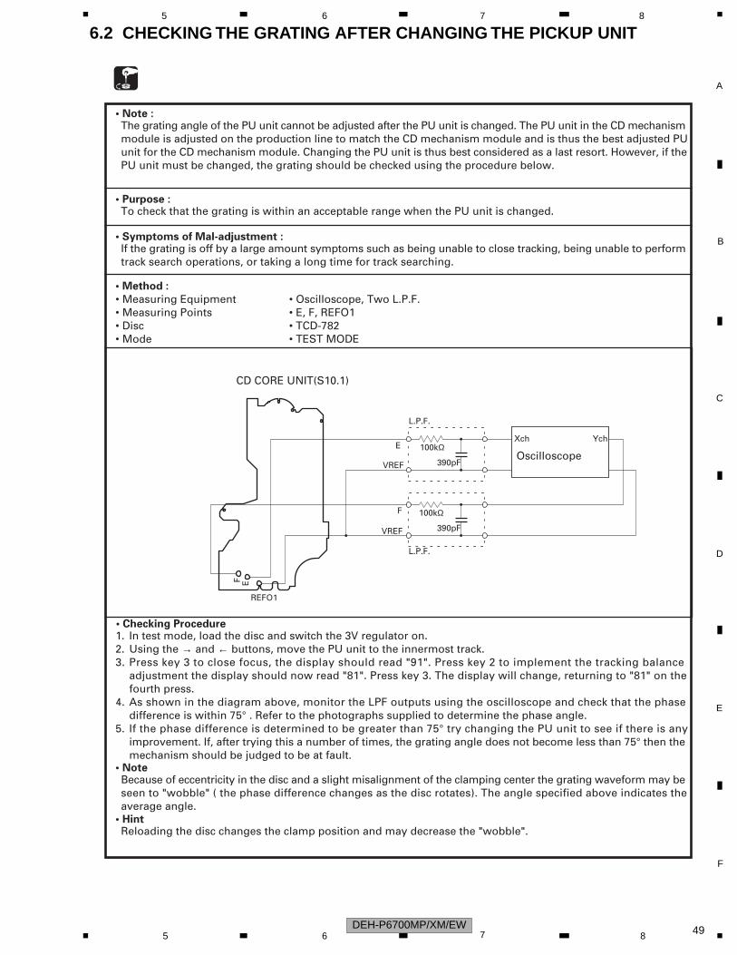
6.2 CHECKING THE GRATING AFTER CHANGING THE PICKUP UNIT
• Note :The grating angle of the PU unit cannot be adjusted after the PU unit is changed. The PU unit in the CD mechanism module is adjusted on the production line to match the CD mechanism module and is thus the best adjusted PU unit for the CD mechanism module. Changing the PU unit is thus best considered as a last resort. However, if the PU unit must be changed, the grating should be checked using the procedure below.
• Purpose :To check that the grating is within an acceptable range when the PU unit is changed.
• Symptoms of Mal-adjustment :If the grating is off by a large amount symptoms such as being unable to close tracking, being unable to perform track search operations, or taking a long time for track searching.
• Method :
• Measuring Equipment• Measuring Points
• Oscilloscope, Two L.P.F.• E, F, REFO1
• Disc • TCD-782• Mode • TEST MODE
• Checking Procedure1. In test mode, load the disc and switch the 3V regulator on.2. Using the → and ← buttons, move the PU unit to the innermost track.3. Press key 3 to close focus, the display should read "91". Press key 2 to implement the tracking balance adjustment the display should now read "81". Press key 3. The display will change, returning to "81" on the fourth press.4. As shown in the diagram above, monitor the LPF outputs using the oscilloscope and check that the phase difference is within 75° . Refer to the photographs supplied to determine the phase angle.5. If the phase difference is determined to be greater than 75° try changing the PU unit to see if there is any improvement. If, after trying this a number of times, the grating angle does not become less than 75° then the mechanism should be judged to be at fault.• NoteBecause of eccentricity in the disc and a slight misalignment of the clamping center the grating waveform may be seen to "wobble" ( the phase difference changes as the disc rotates). The angle specified above indicates the average angle.
• HintReloading the disc changes the clamp position and may decrease the "wobble".
100kΩ
390pF
100kΩ
390pF
E
VREF
F
VREF
Xch Ych
L.P.F.
L.P.F.
REFO1
F E
CD CORE UNIT(S10.1)
Oscilloscope
DEH-P6700MP/XM/EW 495 6 7 8

C
D
F
A
B
E
1 2 3 4
Grating waveform
45°
0°
75°
60°
30°
90°
Ech → Xch 20mV/div, ACFch → Ych 20mV/div, AC
DEH-P6700MP/XM/EW501 2 3 4

C
D
F
A
B
E
5 6 7 8
6.3 ERROR MODE
- Error Messages
Error is displayed with number for Error cause when CD is inoperative or stops with Error during operation.The purpose is to reduce nonsense calls from users as well as to assist all related analysis and repair for defects at service station.
(1) Basic Display Method
1) When CSMOD (CD mode area for system) is SERRORM, Error code will be written in DMIN (minutes area for display), DSEC (seconds area for display). The same data shall be written in DMIN and DSEC. DTNO is blank as usual.
2) Display Example of Head Unit
The following is about LCD display ability. xx is Error number.
8 digits 6 digits 4 digits
ERROR–xx ERR–xx E–xx
(2) Error Code List
No. Classification Contents Details • Cause
10 Electricity Carriage Home NG CRG can’t move to the inner.
CRG can’t move from the inner.
→ HOME SW failure, CRG movement failure.
11 Electricity Focus Search NG Focus can’t be caught.
→ Back of Disc / Severe dirt and vibration.
23 Disc File Format NG Contents are stored in an incompatible file format.
→ The contents in a CD-ROM disc inserted are recorded in a file format other than ISO9660 Level-1 and 2.
22 Disc Impossible to play There is no playable MP3 or WMA file present in a disc.
→ No MP3 or WMA file exists in a CD-ROM disc inserted.
17 Electricity Setup NG AGC protection doesn’t work, out of Focus soon.
→ Scratch on Disc/Severe dirt and vibration.
12 Electricity Spindle Lock NG Not spindle, lock. Wrong subcode (can’t read).
Subcode NG
RF-amp NG
→ Defective Spindle. Scratch and dirt on Disc. Intense vibration.
The appropriate gain of the RF amp cannot be obtained.
→ Defective spindle.
→ Blanc CD-R disc. Disc inserted upside down.
→ Scratched or dirty disc. Severe vibration. Abnormal CD signals.
30 Electricity Search Time Out Can’t reach the target address.
→ Defective CRG/tracking, or scratch on Disc.
→ All TRK Nos. In a disc inserted are specified as a track which should be skipped, in the track skip information.
44 Disc Impossible to play There is no playable TRK No. present in a disc.
50 Mecha Disc Load / Eject NG Disc loading/ejection cannot be complete.
→ Foreign objects entered into the mechanism. Disc caught in between during loading/ejection.
A0 System Power NG Power supply (VD) isn’t connected to the ground.
→ Defective SW transistor. Abnormal power (failed connector)
OR
Err–xx
Note : Error doesn’t display in mechanism only. (CD off causes mechanism off) If TOC can’t be read, error wouldn’t occur, but mechanism still continues its operation. The upper digits of error code is mainly classified by 3 kinds as follows: 1x: Setup related error, 3x: Search related error, Ax: Other errors.
DEH-P6700MP/XM/EW 515 6 7 8

C
D
F
A
B
E
1 2 3 4
7. GENERAL INFORMATION7.1 DIAGNOSIS7.1.1 DISASSEMBLY
- Removing the CD Mechanism Module (Fig.1)
1
Fig.1
- Removing the Case (not shown)
Grille Assy
- Removing the Grille Assy (Fig.1)
1. Remove the Case.
CD Mechanism Module
1
1
1
1
Fig.2Tuner Amp Unit
- Removing the Tuner Amp Unit (Fig.2)
Remove the screw.1
Remove the four screws.
Disconnect the connector and then remove theCD Mechanism Module.
2 Remove the two screws and then remove the Grille Assy.
2 2
1
22
2
3 33
4
Remove the three screws.2
Straighten the tabs at three locations indicated.
3
Remove the screw and then remove the Tuner Amp Unit.
4
DEH-P6700MP/XM/EW521 2 3 4

C
D
F
A
B
E
5 6 7 8
- How to hold the Mechanism Unit1. Hold the top and bottom frame.2. Do not squeeze top frame's front portion too tight, because it is fragile.
- Removing the Upper and Lower Frames1. With a disc clamped, remove the four springs (A), the two springs (B), the two springs (C), and the four screws.2. To remove the upper frame, open it on the fulcrum A.3. While lifting the carriage mechanism, remove the three dampers.4. With the frames removed, insert the connectors coming from the main unit and eject the disc.Caution: Before installing the carriage mechanism in the frames, be sure to apply some alcohol to the dampers and set the mechanism to the clamp mode.
Do not squeeze.
Lower FrameDamper
Carriage Mechanism
A
C
A
B
B
Damper
Damper
C
A
A
A
Upper Frame
DEH-P6700MP/XM/EW 535 6 7 8

C
D
F
A
B
E
1 2 3 4
- Removing the Pickup Unit1. Apply shorting solder to the Pickup flexible cable. Disconnect the cable.2. Set the mechanism to the clamp mode.3. Remove the lead wires from the inner holder.4. Remove the washer, styling holder, change arm, and pickup lock arm.5. While releasing from the hook of the inner holder, lift the end of the feed screw.Caution: In assembling, move the planet gear to the load/eject position before setting the feed screw in the inner holder.
Shorting Solder
Planet Gear
Change Arm
Inner Holder
Styling Holder
Feed Screw
Washer
Pickup Lock Arm
DEH-P6700MP/XM/EW541 2 3 4
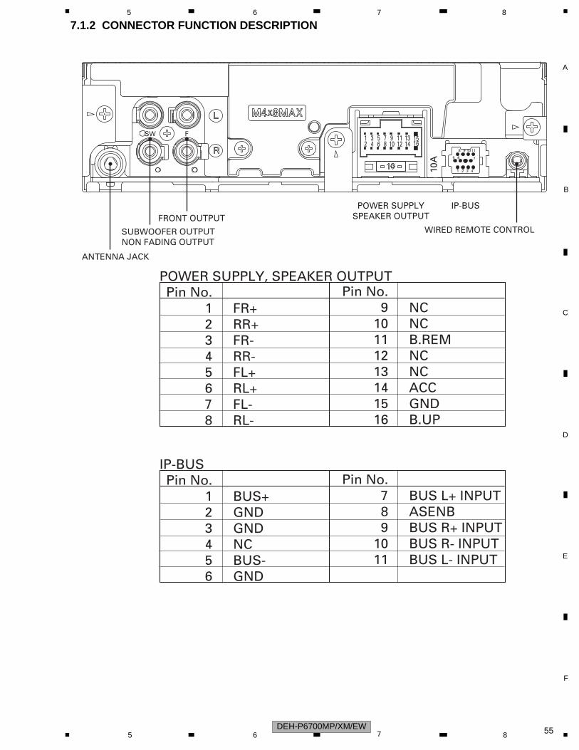
C
D
F
A
B
E
5 6 7 8
7.1.2 CONNECTOR FUNCTION DESCRIPTION
Pin No.12345678
FR+RR+FR-RR-FL+RL+FL-RL-
Pin No.9
10111213141516
NCNCB.REMNCNCACCGNDB.UP
POWER SUPPLY, SPEAKER OUTPUT
Pin No.123456
BUS+GNDGNDNCBUS-GND
Pin No.789
1011
BUS L+ INPUTASENBBUS R+ INPUTBUS R- INPUTBUS L- INPUT
IP-BUS
ANTENNA JACK
WIRED REMOTE CONTROL
10A
1 15162
SUBWOOFER OUTPUTNON FADING OUTPUT
FRONT OUTPUT
34
56
78
910
1112
1314
SW F
111098
765
4321
IP-BUSPOWER SUPPLYSPEAKER OUTPUT
DEH-P6700MP/XM/EW 555 6 7 8

C
D
F
A
B
E
1 2 3 4
7.2 PARTS7.2.1 IC
- Pin Functions (PE5468A)Pin No. Pin Name I/O
1 swvdd O2-4 NC
56 LCDPW7 TELIN8 ejectin I
IOI
9 FLPILM O10 dalmon O11 reset I12 XT213 XT1 I14 VSS15 X216 X117 REGOFF I18 REGC
TESTIN
19 VDD20 ILMPW21 SYSPW O
O
I
22 ADPW O23 NC24 IPPW O25 NC26 ROMDATA I/O27 ROMCLK28 ROMCS O
O
29-31 NC
35
32 tunpce@ O
VDT36 NC
O
37 mute O38,39 NC
40 VSS41 VDD42
46 DORAON O47 NC48 CSENSOUT O
49-55 NC56,57 ROT1,0 I
58 STRKEY2 I59 RGBST
62 PCL O63 BRXEN I/O64 BSRQ65 TSCK/BSCK O
I
66 TSI/BSI67 BSO O
I
68 BRST O
34 VCK O33 VST O
Function and Operation Grille : Chip enable output Not used Test program mode input Not used Telephone mute input Eject sense input Flap illumination output For consumption low-current output Reset input Not used Clock connection pin GND Crystal oscillator connection pin Crystal oscillator connection pin Regulator operation specification signal input Capacitor for regulator connect pin Power supply Illumination power supply control output System power control output A/D converter power supply control output Not used Power supply control output for IP BUS interface IC Not used ROM correction data input/output Not used Not used Not used PLL chip enable output2 E.VOL : Strobe output E.VOL : Clock output E.VOL : Data output Not used System mute output Not used GND Power supply RDS : 57kHz pulse count inputRDS : Decoder reset outputRDS : LOCK input L : RDS signal ONRDS : Data inputNot used Not used CSENS state output Not used Rotary encoder pulse input 1,0 Steering remote controller input RGB strobe outputRGB clock outputRGB data outputClock adjustment output P-BUS : Reception enable input/output P-BUS : Service request input P-BUS : Serial clock output P-BUS : Serial data input P-BUS : Serial data output P-BUS : Reset output Not used
434445
RDS57K Idrst Ordslk IRDT I
60 RGBCK61 RGBDT
69,70 NC
OOO
DEH-P6700MP/XM/EW561 2 3 4

C
D
F
A
B
E
5 6 7 8
Pin No. Pin Name I/O
30
31 50
51
80
81100
1
* PE5468A
IC's marked by * are MOS type.Be careful in handling them because they are very liable to be damaged by electrostatic induction.
BD4834G
1 2 3
VD
D
GN
D
5 4
VO
UT
N.C
.
N.C
.
Vref
Function and Operation IP-BUS : Slave power supply control output Not used GND TUNER : Signal level input Steering remote controller input Not used Flap close sense input Not used A/D converter power supply terminal A/D converter reference voltage terminal GND IP-BUS : Data input IP-BUS : Data output GND RDS : PLL lock detection output RDS : RDS clock input Grille detach sense input Not used ACC power sense input Back up power sense input PLL IC data input Grille data input Grille data output PLL clock output PLL data output PLL chip enable output Beep tone output
76 NC77 CSENS I
78-8182 AVDD83 AVREF84 AVSS O85 RX I86 TX O87 NMI I88 LDET
NC
89 RCK
I
90 dsens I91 NC92 asens93 bsens94 TUNPDI I95 KYDT96 DPDT O97 TUNPCK98 TUNPDO O
O
I
I
99 TUNPCE O100 BEEP O
I73 TESTI74 SL
75 STRKEY1 I
IO
71 ASENSBO O72 EMUTE
DEH-P6700MP/XM/EW 575 6 7 8

C
D
F
A
B
E
1 2 3 4
- Pin Functions(PD6340A)Pin No. Pin Name I/O Function and Operation
1-5 SEG4-0 O LCD segment output6-9 COM3-0 O LCD common output 10 VLCD LCD drive power supply
11-14 KST3-0 O Key strobe output15,16 KDT0,1 I Key data input (analogue input)
17 REW I Remote control reception input18 DPDT I Display data input19 NC Not used20 KYDT O Key data output21 MODA GND22 X0 Crystal oscillator connection pin23 X1 Crystal oscillator connection pin24 VSS GND
25,26 KDT2,3 I Key data input27 NC Not used28 KST4 O Key strobe output
29-32 NC Not used33-55 SEG35-13 O LCD segment output
56 VDD Power supply57-64 SEG12-5 O LCD segment output
* PD6340A
NJM2388F84
49
48 33
32
17
161
64
DEH-P6700MP/XM/EW581 2 3 4
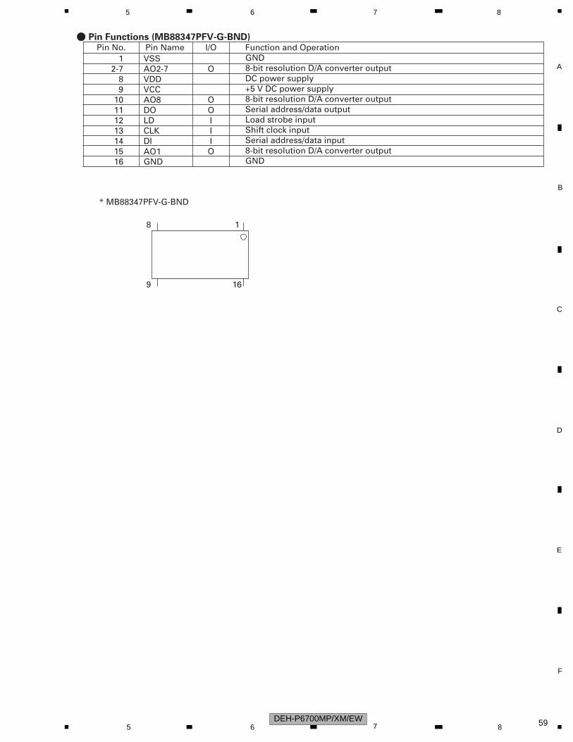
C
D
F
A
B
E
5 6 7 8
- Pin Functions (MB88347PFV-G-BND)Pin No. Pin Name I/O
1 VSS2-7 AO2-7 O
89 VCC
10 AO811 DO O
O
12 LD I13 CLK I14 DI I15 AO1 O16 GND
VDD
Function and Operation GND8-bit resolution D/A converter outputDC power supply+5 V DC power supply8-bit resolution D/A converter outputSerial address/data outputLoad strobe inputShift clock inputSerial address/data input8-bit resolution D/A converter outputGND
* MB88347PFV-G-BND
18
9 16
DEH-P6700MP/XM/EW 595 6 7 8
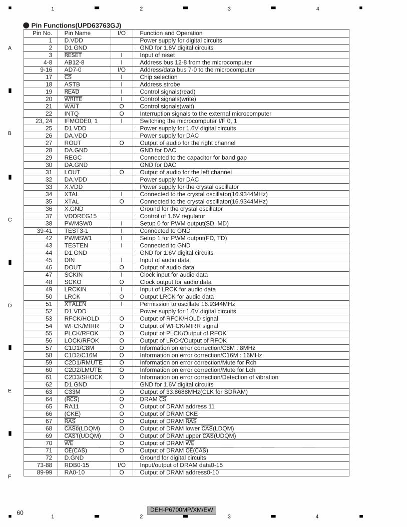
C
D
F
A
B
E
1 2 3 4
- Pin Functions(UPD63763GJ) Pin No. Pin Name I/O Function and Operation 1 D.VDD Power supply for digital circuits 2 D1.GND GND for 1.6V digital circuits 3 reset I Input of reset 4-8 AB12-8 I Address bus 12-8 from the microcomputer 9-16 AD7-0 I/O Address/data bus 7-0 to the microcomputer 17 cs I Chip selection 18 ASTB I Address strobe 19 read I Control signals(read) 20 write I Control signals(write) 21 wait O Control signals(wait) 22 INTQ O Interruption signals to the external microcomputer 23, 24 IFMODE0, 1 I Switching the microcomputer I/F 0, 1 25 D1.VDD Power supply for 1.6V digital circuits 26 DA.VDD Power supply for DAC 27 ROUT O Output of audio for the right channel 28 DA.GND GND for DAC 29 REGC Connected to the capacitor for band gap 30 DA.GND GND for DAC 31 LOUT O Output of audio for the left channel 32 DA.VDD Power supply for DAC 33 X.VDD Power supply for the crystal oscillator 34 XTAL I Connected to the crystal oscillator(16.9344MHz) 35 xtal O Connected to the crystal oscillator(16.9344MHz) 36 X.GND Ground for the crystal oscillator 37 VDDREG15 Control of 1.6V regulator 38 PWMSW0 I Setup 0 for PWM output(SD, MD) 39-41 TEST3-1 I Connected to GND 42 PWMSW1 I Setup 1 for PWM output(FD, TD) 43 TESTEN I Connected to GND 44 D1.GND GND for 1.6V digital circuits 45 DIN I Input of audio data 46 DOUT O Output of audio data 47 SCKIN I Clock input for audio data 48 SCKO O Clock output for audio data 49 LRCKIN I Input of LRCK for audio data 50 LRCK O Output LRCK for audio data 51 xtalen I Permission to oscillate 16.9344MHz 52 D1.VDD Power supply for 1.6V digital circuits 53 RFCK/HOLD O Output of RFCK/HOLD signal 54 WFCK/MIRR O Output of WFCK/MIRR signal 55 PLCK/RFOK O Output of PLCK/Output of RFOK 56 LOCK/RFOK O Output of LRCK/Output of RFOK 57 C1D1/C8M O Information on error correction/C8M : 8MHz 58 C1D2/C16M O Information on error correction/C16M : 16MHz 59 C2D1/RMUTE O Information on error correction/Mute for Rch 60 C2D2/LMUTE O Information on error correction/Mute for Lch 61 C2D3/SHOCK O Information on error correction/Detection of vibration 62 D1.GND GND for 1.6V digital circuits 63 C33M O Output of 33.8688MHz(CLK for SDRAM) 64 (rcs) O DRAM cs 65 RA11 O Output of DRAM address 11 66 (CKE) O Output of DRAM CKE 67 ras O Output of DRAM ras 68 cas)(LDQM) O Output of DRAM lower cas(LDQM) 69 cas!(UDQM) O Output of DRAM upper cas(UDQM) 70 we O Output of DRAM we 71 oe(cas) O Output of DRAM oe(cas) 72 D.GND Ground for digital circuits 73-88 RDB0-15 I/O Input/output of DRAM data0-15 89-99 RA0-10 O Output of DRAM address0-10
DEH-P6700MP/XM/EW601 2 3 4
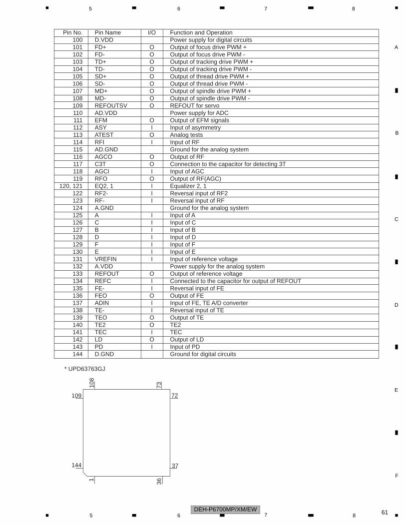
C
D
F
A
B
E
5 6 7 8
Pin No. Pin Name I/O Function and Operation 100 D.VDD Power supply for digital circuits 101 FD+ O Output of focus drive PWM + 102 FD- O Output of focus drive PWM - 103 TD+ O Output of tracking drive PWM + 104 TD- O Output of tracking drive PWM - 105 SD+ O Output of thread drive PWM + 106 SD- O Output of thread drive PWM - 107 MD+ O Output of spindle drive PWM + 108 MD- O Output of spindle drive PWM - 109 REFOUTSV O REFOUT for servo 110 AD.VDD Power supply for ADC 111 EFM O Output of EFM signals 112 ASY I Input of asymmetry 113 ATEST O Analog tests 114 RFI I Input of RF 115 AD.GND Ground for the analog system 116 AGCO O Output of RF 117 C3T O Connection to the capacitor for detecting 3T 118 AGCI I Input of AGC 119 RFO O Output of RF(AGC) 120, 121 EQ2, 1 I Equalizer 2, 1 122 RF2- I Reversal input of RF2 123 RF- I Reversal input of RF 124 A.GND Ground for the analog system 125 A I Input of A 126 C I Input of C 127 B I Input of B 128 D I Input of D 129 F I Input of F 130 E I Input of E 131 VREFIN I Input of reference voltage 132 A.VDD Power supply for the analog system 133 REFOUT O Output of reference voltage 134 REFC I Connected to the capacitor for output of REFOUT 135 FE- I Reversal input of FE 136 FEO O Output of FE 137 ADIN I Input of FE, TE A/D converter 138 TE- I Reversal input of TE 139 TEO O Output of TE 140 TE2 O TE2 141 TEC I TEC 142 LD O Output of LD 143 PD I Input of PD 144 D.GND Ground for digital circuits
* UPD63763GJ
72
73108
109
36
37
1
144
DEH-P6700MP/XM/EW 615 6 7 8

C
D
F
A
B
E
1 2 3 4
- Pin Functions(PE5454A) Pin No. Pin Name I/O Format Function and Operation 1 AVREF A power supply Positive power supply(5V) 2 AVSS A power supply GND 3 RFOK O C Output of state of RFOK 4 NC Not used 5 EVDD E power supply Positive power supply 6, 7 NC Not used 8 IC/FLMD0 IC : VSS direct connection/FLMOD0 : Pull-down 9 VDD Positive power supply(5V) 10 REGC Connected to the capacity stabilizing output of the regulator 11 VSS GND 12 X1 I Oscillator connection for mainclock 13 X2 Oscillator connection for mainclock 14 reset I System reset input 15 XT1 I Connected to the oscillator for subclock (connected to VSS via the resistor) 16 XT2 Connected to the oscillator for subclock(Open) 17 NC Connected to EVDD or EVSS via the resistor 18 NC Not used 19 xint C CD LSI interruption signal input 20 NC Connected to VSS via the resistor 21 brst I P-Bus reset input 22 BSI I P-Bus serial data input 23 BSO O C P-Bus serial data output 24 bsck I/O /C P-Bus serial clock input/output 25 FTXD O C For flash rewriting(transmitted signal) 26 FRXD I For flash rewriting(received signal) 27 BRXEN I/O /C It is possible to receive P-Bus 28 bsrq I/O /C P-Bus service request demand 29 NC Not used 30 DSCSNS I Disc state sense input 31 8EJ(S905) I Input of detection of 8 cm disc ejection 32 12EJ(S904) I Input of detection of 12 cm disc ejection 33 EVSS E power supply GND 34 EVDD E power supply Positive power supply 35, 36 SRAMLEVEL0, 1 O C SRAM level meter output 37 EMPH O C Emphasis information output 38 emph O C Emphasis information output 39-42 NC Not used 43 adena O C A/D reference voltage supply control output 44 LRCKOK O C (DOUT mute output) 45 SRAMLEVEL2 O C SRAM level meter output 46 CD3VON O C CD +3.3V power supply control output 47 CONT O C Servo driver power supply control output 48 xrst O C CD LSI reset control output 49 VDCONT O C VD power supply control output 50 ROMDATA I/O /C E2PROM data input/output 51 ROMCS O C E2PROM chip selection output 52 ROMCK O C E2PROM clock output 53 LOEJ O C The direction change output of LOAD/EJECT 54 CLCONT O C Driver input change output 55 CDMUTE O C CD mute control output 56-58 NC Not used 59 xcs O C CD LSI chip selection output 60 NC Not used 61 xwait I CD LSI write control signal output 62 CLKOUT O C Internal system clock output(Open) 63 LOCK I Spindle lock input 64 NC Not used 65 xwrite O CD LSI write control signal output 66 NC Not used
DEH-P6700MP/XM/EW621 2 3 4

C
D
F
A
B
E
5 6 7 8
Pin No. Pin Name I/O Format Function and Operation 67 xread O CD LSI read control signal output 68 XASTB O CD LSI address strobe output 69 BVSS B power supply GND 70 BVDD B power supply Positive power supply 71-83 AD0-12 I/O /C Address/data Bus 0-12 84-86 NC Not used 87 FMODE I For flash rewriting Connected to VSS via the resistor 88 FLRQ O C For flash rewriting 89-93 NC Not used 94 csens I Flap closing sense input 95 TYPE_A/D I CD-DA analog/digital output change setup 96 testin I Chip check test program starting input 97 HOME I Home SW sense input 98 TEMP Temperature information sense input 99 VDSENS VD power supply short sense input 100 NC Not used
* PE5454A
25
26
50
5175
76
100
1
NJM2885DL1-33
Format Meaning
C CMOS
IN
1
GND
2
OUT
3
BandgapReference
ThermalProtection
+-
DEH-P6700MP/XM/EW 635 6 7 8

C
D
F
A
B
E
1 2 3 4
No. Symbol I/O Explain1 AMANT I AM antenna input AM antenna input high impedance AMANT pin is connected with
an all antenna by way of 4.7µH. (LAU type inductor) A series circuit including an inductor and a resistor is connected with RF ground for the countermeasure against the hum of power transmission line.
2 RFGND RF ground Ground of antenna block3 FMANT I FM antenna input Input of FM antenna 75Ω Surge absorber(DSP-201M-S00B) is necessary.4 VCC power supply The power supply for analog block. D.C 8.4V ± 0.3V5 SL O signal level Output of FM/AM signals level6 CE2 I chip enable-2 Chip enable for EEPROM ”Low” active7 WC I write control You can write EEPROM, when EEPROM write control is “Low”.
Ordinary non connection8 CE1 I chip enable-1 Chip enable for AF•RF ”High” active9 CK I clock Clock
10 DI I data in Data input11 LDET O lock detector “Low” active12 OSCGND osc ground Ground of oscillator block13 ROM_VDD power supply Power supply for EEPROM pin 13 is connected with a power supply of
micro computer.14 DO O data out Data output15 DGND digital ground Ground of digital block16 NC non connection Not used17 VDD_3.3 power supply The power supply for digital block. 3.3V ± 0.2V18 RDS_CK O RDS clock Output of RDS clock(2.5V)19 RDS_DATA O RDS data Output of RDS data(2.5V)20 RDS_LOCK O RDS lock Output unit “High” active(2.5V) (RDS_LOCK turns over by the
external transistor. “Low” active)21 RDS_HSLK O RDS high speed Output unit “High” active(2.5V)(RDS_HSLK turns over by the
lock external transistor. “Low” active)22 AUDIOGND audio ground Ground of audio block23 L ch O L channel output FM stereo “L-ch” signal output or AM audio output 24 R ch O R channel output FM stereo “R-ch” signal output or AM audio output
FMRF
ANT adjRF adj
FM ANT
T51 CF52CF51
RFG
ND
OS
CG
ND
DG
ND
AU
DIO
GN
D
NC
VC
C
VD
D_3
.3
3.3V 2.5VIC 4
3.3V 2.5V
←
IC 22.5V
WC
CE
2
RO
M_V
DD SL DI
CK
CE
1
LDE
T
DO
RD
S_C
K
RD
S_D
ATA
RD
S_L
OC
K
RD
S_H
SLK
7 6 13 5 10 9 8 11 14 18 19 20 21
1
3
2 12 15 22 16 4 17
IC 13.3V
AM ANT FMRFATT
LPFOSC
IC 3 EEPROM5.0V
IC 55V 3.3V←
ATT
MIXER, IF AMP DET, FM MPX,RDS DECODER
24
23
Rch
Lch
- FM/AM Tuner Unit
DEH-P6700MP/XM/EW641 2 3 4

C
D
F
A
B
E
5 6 7 8
7.2.2 DISPLAY
- LCD(CAW1865)
SE
GM
EN
T
CO
MM
ON
COM 0
COM 1
COM 2
COM 3
SEG0
SEG1
SEG2
SEG3
SEG4
SEG5
SEG6
SEG7
SEG8
SEG9
SEG10
SEG11
SEG12
SEG13
SEG14
SEG15
SEG16
SEG17
SEG18
SEG19
SEG20
SEG21
SEG22
SEG23
SEG24
SEG25
SEG26
SEG27
SEG28
SEG29
SEG30
SEG31
SEG32
SEG33
SEG34
SEG35
COM0
COM1
COM2
COM3
SEG36
SEG37
SEG38
SEG39
DEH-P6700MP/XM/EW 655 6 7 8

C
D
F
A
B
E
1 2 3 4
7.3 OPERATIONAL FLOW CHART
VDD=5VPin 19, 41
ASENSBO←HPin 71
Power ON
bsens=L
asens=L
dsens=L
bsensPin 93
asensPin 92
dsensPin 90
swvdd←LPin 1
Source keys operative
Completes power-on operation.(After that, proceed to each source operation)
SYSPW←HPin 21
Startscommunication
with Grillemicrocomputer.
Source ON
300ms
300ms
In case of the above signal, the communication with Grille microcomputer may fail.If the time interval is not 300msec, the oscillator may be defective.
CSENSPin 77
2V < CSENS < 3V
- CSENS 2V, 3V CSENS Last source returns. CD loading functions are available. Keys except for EJECT key are not available.
< <= =
DEH-P6700MP/XM/EW661 2 3 4

C
D
F
A
B
E
5 6 7 8
7.4 CLEANING
Before shipping out the product, be sure to clean the following portions by using the prescribed cleaning tools:
Portions to be cleaned Cleaning tools
CD pickup lenses Cleaning liquid : GEM1004
Cleaning paper : GED-008
DEH-P6700MP/XM/EW 675 6 7 8

C
D
F
A
B
E
1 2 3 4
8. OPERATIONS
DEH-P6700MP/XM/EW681 2 3 4

C
D
F
A
B
E
5 6 7 8
DEH-P6700MP/XM/EW 695 6 7 8

C
D
F
A
B
E
1 2 3 4
DEH-P6700MP/XM/EW701 2 3 4

C
D
F
A
B
E
5 6 7 8
DEH-P6700MP/XM/EW 715 6 7 8

C
D
F
A
B
E
1 2 3 4
DEH-P6700MP/XM/EW721 2 3 4
C
D
F
A
B
E
5 6 7 8
DEH-P6700MP/XM/EW 735 6 7 8

C
D
F
A
B
E
1 2 3 4
DEH-P6700MP/XM/EW741 2 3 4

C
D
F
A
B
E
5 6 7 8
Fixing the front panel
If you do not operate the removing and attaching the front panel function, use the suppliedfixing screws and holders to fix the front panel to this unit.
1. Attach the holders to both sides of the front panel.
2. Replace the front panel to the unit.
3. Flip the holders into upright positions.
4. Fix the front panel to the unit using fixing screws.
Fixing ScrewBPZ20P060FZK
HolderCND1249 Holder
CND1250
DEH-P6700MP/XM/EW 755 6 7 8

C
D
F
A
B
E
1 2 3 4
Cap
(1*)
Whe
nno
tusi
ngth
iste
rmin
al,
dono
trem
ove
the
cap.
ISO
conn
ecto
rN
ote:
Inso
me
vehi
cles
,the
ISO
conn
ecto
rm
aybe
divi
ded
into
two.
Inth
isca
se,b
esu
reto
conn
ectt
obo
thco
nnec
tors
.
1*
2* 4*
3* 5*
Yel
low
(2*)
Tote
rmin
alal
way
ssu
pplie
dw
ithpo
wer
rega
rdle
ssof
igni
tion
switc
hpo
sitio
n.
Red
(4*)
Toel
ectr
icte
rmin
alco
ntro
lled
byig
nitio
nsw
itch
(12
VD
C)
ON
/OFF
.
Yel
low
(3*)
Bac
k-up
(or
acce
ssor
y)
Red
(5*)
Acc
esso
ry(o
rba
ck-u
p)
Bla
ck(g
roun
d)To
vehi
cle
(met
al)
body
.
.
Blu
e/w
hite
(7*)
ToA
uto-
ante
nna
rela
yco
ntro
lter
min
al(m
ax.3
00m
A12
VD
C).
Not
e:D
epen
ding
onth
eki
ndof
vehi
cle,
the
func
tion
of3*
and
5*m
aybe
diff
eren
t.In
this
case
,be
sure
toco
nnec
t2*
to5*
and
4*to
3*.
Subw
oofe
r
Left
Rig
ht
Blu
e/w
hite
(6*)
The
pin
posi
tion
ofth
eIS
Oco
nnec
tor
will
diff
erde
pend
son
the
type
ofve
hicl
e.C
onne
ct6*
and
7*w
hen
Pin
5is
anan
tenn
aco
ntro
ltyp
e.In
anot
her
type
ofve
hicl
e,ne
ver
conn
ect6
*an
d7*
.
Con
nect
ing
cord
sw
ithR
CA
pin
plug
s(s
old
sepa
rate
ly)
Thi
spr
oduc
t
Fuse
IP-B
US
cabl
e
IP-B
US
inpu
t(B
lue)
Ant
enna
jack
Con
nect
lead
sof
the
sam
eco
lor
toea
chot
her
Jack
for
the
Wir
ed R
emot
e C
ontr
olPl
ease
see
the
Inst
ruct
ion
Man
ual f
or th
eW
ired
Rem
ote
Con
trol
(so
ld s
epar
atel
y).
Blu
e/w
hite
To s
yste
m c
ontr
ol te
rmin
al o
f th
e po
wer
amp
(max
. 300
mA
12
V D
C).
Yel
low
/bla
ckIf
you
use
ace
llula
rte
leph
one,
conn
ecti
tvia
the
Aud
ioM
ute
lead
onth
ece
llula
rte
leph
one.
Ifno
t,ke
epth
eA
udio
Mut
ele
adfr
eeof
any
conn
ectio
ns.
Perf
orm
thes
eco
nnec
tions
whe
nus
ing
the
optio
nal a
mpl
ifie
r.
Pow
eram
p(s
old
sepa
rate
ly)
Syst
emre
mot
eco
ntro
l
Fron
t out
put
(FR
ON
T O
UT
PUT
)
Mul
ti-C
Dpl
ayer
(sol
dse
para
tely
)
Fron
t Spe
aker
Fron
t Spe
aker
Subw
oofe
r
Pow
eram
p(s
old
sepa
rate
ly)
Subw
oofe
r ou
tput
or
non
fadi
ng o
utpu
t
Spea
ker
lead
sW
hite
Whi
te/b
lack
Gra
yG
ray/
blac
kG
reen
Gre
en/b
lack
Vio
let
Vio
let/b
lack
:Fro
ntle
ft+
:Fro
ntle
ft≠
:Fro
ntri
ght +
:Fro
ntri
ght ≠
:Rea
rle
ft+
:Rea
rle
ft≠
≠:R
ear
righ
t+
+:R
ear
righ
t≠
≠
or S
ubw
oofe
r+
or S
ubw
oofe
ror
Sub
woo
fer
or S
ubw
oofe
rC
hang
e th
e in
itial
set
ting
of th
is u
nit
(ref
er to
the
oper
atio
nal M
anua
l).
The
sub
woo
fer
outp
utof
the
unit
is
mon
aura
l.
Not
e:
DEH-P6700MP/XM/EW761 2 3 4
DEH-P6700MP/XM/EW 77
5 6 7 8
5 6 7 8
C
D
F
A
B
E

C
D
F
A
B
E
1 2 3 4
- Jigs List
Test DiscL.P.F.
TCD-782 Checking the gratingg g gChecking the grating g g g (Two pieces)( )
Name Jig No. Remarks
DEH-P6700MP/XM/EW781 2 3 4