mtxp-945g long life atx industrial motherboard … · obligated to repair, ... the mtxp-945g...
TRANSCRIPT

MTXP-945G Long Life Industrial Motherboard
Revision A
Technical Reference
Intel® Pentium 4 Intel® Pentium D
or Intel® Celeron D
Embedded Processors
Intel 945G Express Chipset

Warranty The product is warranted against material and manufacturing defects for two years from date of delivery. Buyer agrees that if this product proves defective Chassis Plans is only obligated to repair, replace or refund the purchase price of this product at Chassis Plans’ discretion. The warranty is void if the product has been subjected to alteration, neglect, misuse or abuse; if any repairs have been attempted by anyone other than Chassis Plans; or if failure is caused by accident, acts of God, or other causes beyond the control of Chassis Plans. Chassis Plans reserves the right to make changes or improvements in any product without incurring any obligation to similarly alter products previously purchased.
In no event shall Chassis Plans be liable for any defect in hardware or software or loss or inadequacy of data of any kind, or for any direct, indirect, incidental or consequential damages arising out of or in connection with the performance or use of the product or information provided. Chassis Plans’ liability shall in no event exceed the purchase price of the product purchased hereunder. The foregoing limitation of liability shall be equally applicable to any service provided by Chassis Plans.
Return Policy Products returned for repair must be accompanied by a Return Material Authorization
(RMA) number, obtained from Chassis Plans prior to return. Freight on all returned items must be prepaid by the customer, and the customer is responsible for any loss or damage caused by common carrier in transit. Items will be returned from Chassis Plans via Ground, unless prior arrangements are made by the customer for an alternative shipping method.
To obtain an RMA number, call us at (858) 571-4330. We will need the following information:
Return company address and contact Model name and model # from the label on the back of the board Serial number from the label on the back of the board Description of the failure
An RMA number will be issued. Mark the RMA number clearly on the outside of each box, include a failure report for each board and return the product(s) to our San Diego, CA facility:
Chassis Plans 8295 Aero Place San Diego, CA 92123 Attn: Repair Department

TRADEMARKS IBM, PC/AT, VGA, EGA, OS/2 and PS/2 are trademarks or registered trademarks of International Business Machines Corp. Intel is a registered trademark of Intel Corporation. MS-DOS and Microsoft are registered trademarks of Microsoft Corp. PICMG, SHB Express and the PICMG logo are registered trademarks of the PCI
Industrial Computer Manufacturers Group. All other brand and product names may be trademarks or registered trademarks of their
respective companies.
LIABILITY This manual is as complete and factual as possible at the time of printing; however, the DISCLAIMER information in this manual may have been updated since that time. Chassis Plans reserves
the right to change the functions, features or specifications of their products at any time, without notice.
Copyright © 2007 by Chassis Plans. All rights reserved. E-mail: [email protected] Web: www.chassisplans.com
Chassis Plans 8295 Aero Place • San Diego, CA 92123 Sales (858) 571-4330 • Fax (858-571-6146 • Web www.chassisplans.com


MTXP-945G – Technical Reference Introduction
Chassis Plans I
Table of Contents
Notice ....................................................................................................................................... III
Introduction .......................................................................................................................................IV
Chapter 1 Pre-Configuration .........................................................................................................1
Step 1 Setting the Jumpers 2 Jumper Locations...............................................................................................................................3 CMOS Reset ........................................................................................................................................4 ATA-Disk Connector Voltage Selection ...........................................................................................4 RS422/RS485 Termination Resistors (optional)..............................................................................4
Step 2 SDRAM, CPU, and Cables Installation 4 MTXP-945G Memory Configuration..................................................................................................4 CPU Installation..................................................................................................................................5 Installing Cables...............................................................................................................................10 Power and Control Panel Cables ....................................................................................................10 Installing Peripheral Cables ............................................................................................................11 Index of Connectors.........................................................................................................................13
Chapter 2 AMIBIOS Setup ..........................................................................................................15
Main Setup ........................................................................................................................................18 Advanced BIOS Setup .....................................................................................................................18 PCI/PnP Setup...................................................................................................................................27 Boot Setup ........................................................................................................................................29 Security Setup ..................................................................................................................................32 Chipset Setup ...................................................................................................................................34 Exit Menu...........................................................................................................................................37
Chapter 3 Upgrading....................................................................................................................39
Upgrading the Microprocessor .......................................................................................................39 Upgrading the System Memory ......................................................................................................39
Appendix A Technical Specifications............................................................................................41
Chipsets ............................................................................................................................................41 BIOS...................................................................................................................................................41 Embedded I/O ...................................................................................................................................41 Industrial Devices.............................................................................................................................42 Miscellaneous...................................................................................................................................43 Mechanical Drawing.........................................................................................................................44 Memory Map......................................................................................................................................45 DMA Channels ..................................................................................................................................45 I/O Map...............................................................................................................................................45 Interrupts...........................................................................................................................................46 SMBUS...............................................................................................................................................47 PCI Interrupt Routing Map...............................................................................................................47 Connectors Pin-out ..........................................................................................................................47

Introduction MTXP-945G Technical Reference
II Chassis Plans
Appendix B Flash BIOS programming and codes .......................................................................55
Troubleshooting POST ....................................................................................................................56 Critical Error BEEP Codes...............................................................................................................60
Appendix C On-Board Industrial Devices .....................................................................................63
Post Code Display............................................................................................................................63 On-board Ethernet............................................................................................................................63 Serial Ports........................................................................................................................................64
Appendix On-Board Video Controller ........................................................................................69
....................

MTXP-945G Technical Reference Introduction
Chassis Plans III
Notice
Chassis Plans reserves the right to revise this publication or to change its contents without notice. Information contained herein is for reference only and does not constitute a commitment on the part of the manufacturer or any subsequent vendor. They are in no way responsible for any loss or damage resulting from the use (or misuse) of this publication.
This publication and any accompanying software may not, in whole or in part, be copied, photocopied, translated or reduced to any machine readable form without prior consent from the vendor, manufacturer or creators of this publication, except for copies kept by the user for backup purposes.

Introduction MTXP-945G Technical Reference
IV Chassis Plans
Introduction Thank you for your purchase of the MTXP-945G industrial embedded motherboard. The MTXP-945G design is based on the Intel 945G chipset providing the ideal platform for industrial applications. The MTXP-945G design is based on the Intel Pentium 4 processor LGA775 socket (FC-LGA4).
With proper installation and maintenance, your MTXP-945G will provide years of high performance and trouble free operation.
This manual provides a detailed explanation into the installation and use of the MTXP-945G industrial embedded motherboard. This manual is written for the novice PC user/installer. However, as with any major computer component installation, previous experience is helpful and should you not have prior experience, it would be prudent to have someone assist you in the installation. This manual is broken down into 3 chapters and 4 appendixes.
Chapter 1 - System Board Pre-Configuration
This chapter provides all the necessary information for installing the MTXP-945G. Topics discussed include: installing the CPU (if necessary), DRAM installation and jumper settings. Connecting all the cables from the system board to the chassis and peripherals is also explained.
Chapter 2 - BIOS Configuration
This chapter shows the final step in getting your system firmware setup.
Chapter 3 - Upgrading
The MTXP-945G provides a number of expansion options including memory. All aspects of the upgrade possibilities are covered.
Appendix A - Technical Specifications
A complete listing of all the major technical specifications of the MTXP-945G is provided.
Appendix B - Flash BIOS Programming and Codes
Provides all information necessary to program your AMIBIOS Flash BIOS. POST Codes and beep codes are described in details.
Appendix C – On-Board Industrial Devices
One or Two on-board Gigabit Ethernet controller(s), two or six serial ports (one optional RS422/485), hardware monitor, watchdog timer and Post Code Display.
Appendix D - On-Board Video Controller
On-board CRT video controller.

MTXP-945G Technical Reference Introduction
Chassis Plans V
Static Electricity Warning!
The MTXP-945G has been designed as rugged as possible but can still be damaged if jarred sharply or struck. Handle the motherboard with care. The MTXP-945G also contains delicate electronic circuits that can be damaged or weakened by static electricity. Before removing the MTXP-945G from its protective packaging, it is strongly recommended that you use a grounding wrist strap. The grounding strap will safely discharge any static electricity build up in your body and will avoid damaging the motherboard. Do not walk across a carpet or linoleum floor with the bare board in hand. . MTXP-945G - An Overview
The MTXP-945G represents the ultimate in industrial embedded motherboard technology. No other system board available today provides such impressive list of features:
CPU Support
• Supports Intel Pentium 4, Intel Pentium D and Intel Celeron D processors in the LGA775 socket with a 1066, 800 and 566MHz system bus.
Supported Bus Clocks
• 1066, 800 and 566MHz.
Memory
• Four 240-pin DDR2 SDRAM module sockets up to 4GB (non-ECC), DDR2 667, DDR2 533, or DDR2 400 MHz SDRAM DIMMs. Please, refer to chapter 3 for memory details.
On-Board I/O
• 2 Floppies up to 2.88 MB. • Single channel PCI 32-bit EIDE controller – UDMA 66/100 supported. One standard 40-pin header and
one mini-Header 44-pin for Solid State IDE disk or any 44-pin IDE device support shared on the single primary channel.
• Four independent Serial ATA2 ports with transfer rates up to 300 MB/s per port. • Two or optional six high speed RS-232 serial ports 16 Bytes FIFO (16550). COM2 RS-232 IrDA on a
header and COM1 optional RS-422/485. • One bi-directional parallel port. EPP/ECP mode compatible. • One PS/2 mouse and one PS/2 keyboard. • Eight Universal Serial Bus ports, USB 1.1 and USB 2.0 compliant. Four connectors and four headers • Two 32-bit PCI slots, one PCI Express x16 dedicated graphics slot and one PCI Express x4 slot. • One (optional two) PCI Express based Gigabit Ethernet controllers. • Automatic CPU voltage & temperature monitoring device. • On-board Buzzer. • Intel HD Audio. Microphone In, Stereo Line In and Out, Aux In and CD In.

Introduction MTXP-945G Technical Reference
VI Chassis Plans
ROM BIOS
• American Megatrends AMIBIOS with FLASH ROM.
On-Board CRT video controller
• Standard CRT video controller (Intel 945G chipset).
Conventions Used in this Manual
Notes - Such as a brief discussion of memory types.
Important Information - such as static warnings, or very important instructions.
When instructed to enter keyboard keystrokes, the text will be noted by this graphic.

MTXP-945G – Technical Reference Chapter 1: Pre-Configuration
Chassis Plans 1
Special Warranty Note: Products returned for warranty repair will be inspected for damage caused by improper installation and misuse as described in the previous section and the static warning below. Should the board show signs of abuse, the warranty will become void and the customer will be billed for all repairs and shipping and handling costs.
Static Warning:
The MTXP-945G contains delicate electronic semiconductors that are highly sensitive to static electricity. These components, if subjected to a static electricity discharge, can be weakened thereby reducing the serviceable life of the system board.
BEFORE THE BOARD IS REMOVED FROM ITS PROTECTIVE ANTISTATIC PACKAGING, TAKE PROPER PRECAUTIONS!
Work on a conductive surface that is connected to ground. Before touching any electronic device, ground yourself by touching an unpainted metal object or, and highly recommended, use a grounding strap. Damage from static electricity is not covered by the warranty.
Chapter 1 Pre-Configuration This chapter provides all the necessary information for installing the MTXP-945G into a standard PC chassis. Topics discussed include: installing the CPU (if necessary), DRAM installation and jumper settings.
Handling Precautions
The MTXP-945G has been designed to be as rugged as possible but it can be damaged if dropped, jarred sharply or struck. Damage may also occur by using excessive force in performing certain installation procedures such as forcing the system board into the chassis or placing too much torque on a mounting screw.
Take special care when installing or removing the system memory DIMMs. Never force a DIMM into a socket. Screwdrivers slipping off a screw and scraping the board can break a trace or component leads, rendering the board unusable. Always handle the MTXP-945G with care.
Static Warning
The MTXP-945G contains delicate electronic semiconductors that are highly sensitive to static electricity. These components, if subjected to a static electricity discharge, can be weakened thereby reducing the serviceable life of the system board. BEFORE THE BOARD IS REMOVED FROM ITS PROTECTIVE ANTISTATIC PACKAGING, TAKE PROPER PRECAUTIONS! Work on a conductive surface that is connected to ground. Before touching any electronic device, ground yourself by touching an unpainted metal object or, and highly recommended, use a grounding strap. Damage from static electricity is not covered by the warranty.
Chapter 1: Pre-Configuration MTXP-945G Technical Reference
2 Chassis Plans
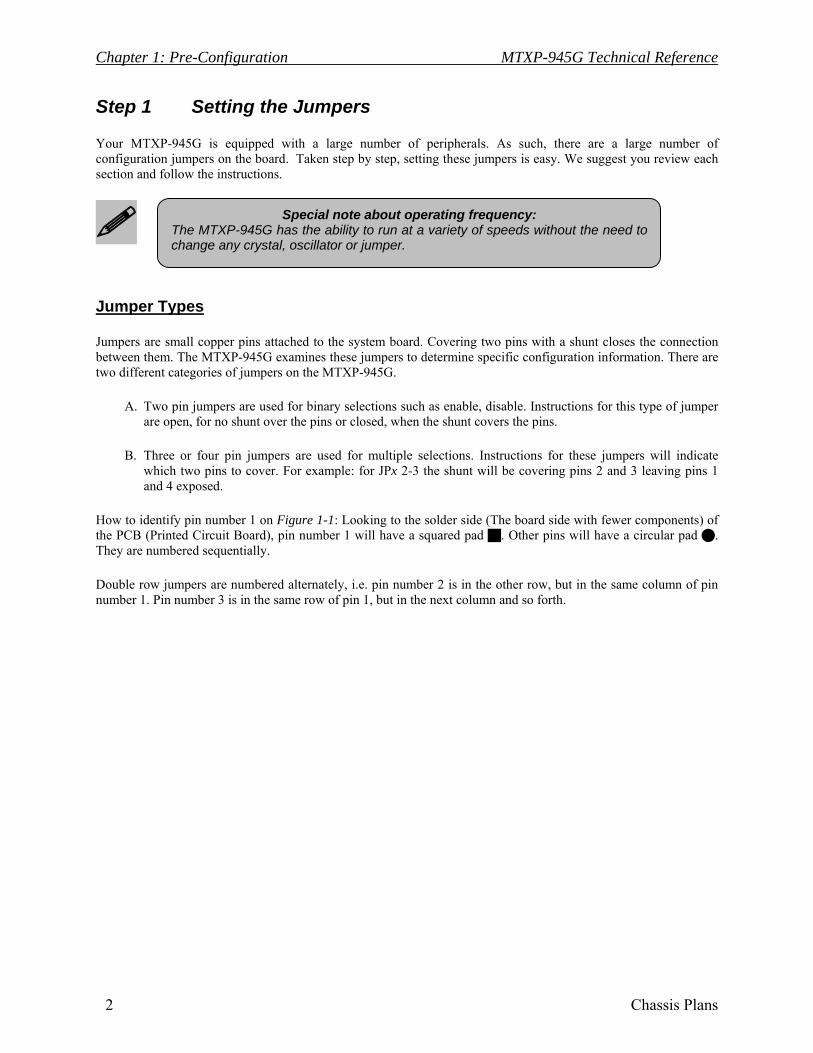
Special note about operating frequency: The MTXP-945G has the ability to run at a variety of speeds without the need to change any crystal, oscillator or jumper.
Step 1 Setting the Jumpers
Your MTXP-945G is equipped with a large number of peripherals. As such, there are a large number of configuration jumpers on the board. Taken step by step, setting these jumpers is easy. We suggest you review each section and follow the instructions.
Jumper Types
Jumpers are small copper pins attached to the system board. Covering two pins with a shunt closes the connection between them. The MTXP-945G examines these jumpers to determine specific configuration information. There are two different categories of jumpers on the MTXP-945G.
A. Two pin jumpers are used for binary selections such as enable, disable. Instructions for this type of jumper are open, for no shunt over the pins or closed, when the shunt covers the pins.
B. Three or four pin jumpers are used for multiple selections. Instructions for these jumpers will indicate which two pins to cover. For example: for JPx 2-3 the shunt will be covering pins 2 and 3 leaving pins 1 and 4 exposed.
How to identify pin number 1 on Figure 1-1: Looking to the solder side (The board side with fewer components) of the PCB (Printed Circuit Board), pin number 1 will have a squared pad . Other pins will have a circular pad . They are numbered sequentially.
Double row jumpers are numbered alternately, i.e. pin number 2 is in the other row, but in the same column of pin number 1. Pin number 3 is in the same row of pin 1, but in the next column and so forth.

MTXP-945G Technical Reference Chapter 1: Pre-Configuration
Chassis Plans 3
Jumper Locations
Use the diagram below and the tables on the following pages to locate and set the on-board configuration jumpers.
Figure 1-1 Jumper Locations

Chapter 1: Pre-Configuration MTXP-945G Technical Reference
4 Chassis Plans
CMOS Reset
This option is provided as a convenience for those who need to reset the CMOS registers. It should always be set to "Normal" for standard operation. If the CMOS needs to be reset, turn off the system power, move JP2 to 2-3, turn the system on, move jumper to 1-2 and press reset.
Table 1-1 CMOS Reset
Reset CMOS Normal Clear CMOS JP2 1-2* 2-3
* Default Settings. ATA-Disk Connector Voltage Selection
The ATA-Disk Connector IDE2 can provide either 5Vcc or 3.3Vcc. The jumper JP1 selects the voltage.
Table 1-2 ATA-Disk Connector Voltage Select
ATA-Disk Voltage 5Vcc 3.3Vcc JP1 1-2* 2-3
* Default Settings. RS422/RS485 Termination Resistors (optional)
The Jumper J6 allows the insertion/removal of the termination resistors (120Ω) in the Receiver and Transmitter lines of the COM1 when operating in RS-422/485 mode.
Table 1-3 COM1 RS-422/485 Tx & Rx Termination Resistor Selection
Termination resistor selection Transmitter Receiver
J6 1-3 2-4 * Default Setting is off. Step 2 SDRAM, CPU, and Cables Installation
Depending upon how your MTXP-945G is configured you may need to install the following:
• SDRAM (DIMMs) • CPU
MTXP-945G Memory Configuration
The MTXP-945G offers 4 DIMM memory sockets (Locations DIMM1,2,3 and 4 – Figure 1-2). They can be configured with 1.8V SDRAM DDR2 DIMM modules. It is very important that the quality of the DIMMs is good. Unreliable operation of the system may result if poor quality DIMMs are used. Always purchase your memory from a reliable source. Please, refer to chapter 3 for memory details.

MTXP-945G Technical Reference Chapter 1: Pre-Configuration
Chassis Plans 5
CPU Installation Warning:
1. Improper installation of the CPU may cause permanent damage to both the system board and the CPU. This will void the warranty.
2. Always handle the CPU by the edges, never touch the pins.
3. Always use a heat-sink and a CPU fan.
CPU Installation
The MTXP-945G currently supports the following CPUs:
• Intel Pentium 4, Intel Pentium D and Intel Celeron D processors in the LGA775 socket with a 1066, 800 and 566MHz system bus.
Locate the CPU socket on your MTXP-945G system board (Socket LGA775 – Figure 1-2). To install a CPU, first turn off your system and remove its cover. Locate the LGA775 socket and open it by first pulling the lever sideways away from the socket then upward to a 90-degree angle. Insert the CPU with the correct orientation as shown below. The notched corner should point toward the end of the lever. Because the CPU has a corner pin for two of the four corners, the CPU will only fit in the orientation as shown. When you put the CPU into the LGA775 socket, no force is required to insert the CPU, and then press the lever to the locked position.
When you install a DIMM module fully into the DIMM socket the eject tab should be locked into the DIMM module very firmly and fit into its indention on both sides.

Chapter 1: Pre-Configuration MTXP-945G Technical Reference
6 Chassis Plans
CPU LGA775 Socket
Colden Arrow
LG
A77
5
The continued push of technology to increase performance levels (higher operating speeds) and packaging density (more transistors) is aggravating the thermal management of the CPU. As operating frequencies increase and packaging sizes decreases, the power density increases and the thermal cooling solution space and airflow become more constrained. The result is an increased importance on system design to ensure that thermal requirements are met for the CPU. The objective of thermal management is to ensure that the temperature of the processor is maintained within functional limits. The functional temperature limit is the range within which the electrical circuits can be expected to meet their specified performance requirements. Operation outside the functional limit can degrade system performance, cause logic errors or cause component and/or system damage. Temperatures exceeding the maximum operating limits may result in irreversible changes in the operating characteristics of the component. If the MTXP-945G industrial embedded motherboard is acquired without the CPU and the heat sink, extreme care must be taken to avoid improper thermal management. All Intel thermal solution specifications, design guidelines and suggestions regarding the CPU being used must be followed. The MTXP-945G warranty is void if the thermal management does not comply with Intel requirements.
Designing for thermal performance In designing for thermal performance, the goal is to keep the processor within the operational thermal specifications. The inability to do so will shorten the life of the processor. Fan Heatsink An active fan heatsink can be employed as a mechanism for cooling the Intel processors. This is the acceptable solution for most chassis. Adequate clearance must be provided around the fan heatsink to ensure unimpeded air flow for proper cooling. Use a plastic cooler back plate when installing the fan cooler assembly on to the CPU Airflow management It is important to manage the velocity, quantity and direction of air that flows within the system (and how it flows) to maximize the volume of air that flows over the processor. Thermal interface management To optimize the heatsink design for the Pentium 4 processor, it is important to understand the impact of factors related to the interface between the processor and the heatsink base. Specifically, the bond line thickness, interface material area, and interface material thermal conductivity should be managed to realize the most effective thermal solution.
Be sure that there is sufficient air circulation across the processor’s heatsink and the CPU cooling FAN is working correctly, otherwise it may cause the processor and motherboard to overheat and damage them. You may install an auxiliary cooling FAN if necessary.

MTXP-945G Technical Reference Chapter 1: Pre-Configuration
Chassis Plans 7
Once used, the thermal interface should be discarded and a new one installed. Never assemble the heatsink with a previously used thermal interface.
LGA 775 CPU Installation Guide
Socket Preparation
1. Opening the socket:
Note: Apply pressure to the corner with right hand thumb while opening/closing the load lever, otherwise the lever can bounce back like a “mouse trap” and WILL cause bent contacts when loaded.
i. Disengage Load Lever by depressing down and out on the hook to clear retention tab
ii. Rotate Load Lever to fully open position at approximately 135 degrees
iii. Rotate Load Plate to fully open position at approximately 100 degrees
2. Remove PnP Cap (Pick & Place Cap)
i. With left hand index finger and thumb to support the load plate edge, engage PnP cap with right hand thumb and peel the cap from LGA775 Socket while pressing on center of PnP cap to assist in removal.
ii. Set PnP cap aside. Always put PnP cap back on if the processor is removed from the socket.
iii. Visually inspect PnP cap for damage. If damage observed, replace the PnP cap.
Note: After PnP cap removal, make sure socket load plate and contacts are free of foreign material; Refer to Overview Module for FM cleaning. Note: Optionally, remove PnP cap after CPU insertion. This will compromise the ability to visually inspect socket.
Socket Load Lever Open
Socket Load Plate Open.

Chapter 1: Pre-Configuration MTXP-945G Technical Reference
8 Chassis Plans
3. Visually inspect for bent contacts (Recommended at least 1st pass visual inspection)
NOTE: Refer to the Handling and Inspection Module for 1st and 2nd pass inspection details.
NOTE: Glove manipulation images are for illustrative purposes only. Please consult local safety guidelines for specific requirements.
NOTE: Recommended not to hold the load plate as a lever, instead hold at tab with left hand, removing the PnP cap with right hand.
775- Land LGA Package Insertion
• Lift processor package from shipping media by grasping the substrate edges ONLY.
Note: Orient processor package such that the Pin 1 triangle mark is on bottom left and both key notches are on left side • Land Side Cover Handling: Remove land side cover with the
opposite hand by depressing larger retention tab and peeling the cover away
• Set the land side cover aside. Note: Always keep the land side cover on the processor when
not in the socket. • Visually inspect the package gold pads: Scan the processor
package gold pad array for presence of foreign material. Refer to Overview Module for FM cleaning recommendations
• Orient the package with IHS up. Locate Pin 1 and the two orientation key notches
• Carefully place the package into the socket body using a purely vertical motion
CAUTION: Using a Vacuum Pen for installation is not recommended • Verify that package is within the socket body and properly
mated to the orient keys • Close the socket by:
1. Rotating the Load Plate onto the package HIS 2. While pressing down lightly on Load Plate, engage the
Load Lever. 3. Securing Load Lever with Load Plate tab under
retention tab of Load Lever
Press to remove
Pin 1 Indicator
Alignment Key

MTXP-945G Technical Reference Chapter 1: Pre-Configuration
Chassis Plans 9
Intel Reference Thermal Solution Assembly NOTE: Depending on the configuration, the Thermal Solution Integration procedure could perform with M/B alone or with M/B in the Chassis.
1. Place motherboard on support structure providing
minimum 0.150-inch backside clearance 2. Apply 300 mg of Thermal Interface Material onto center of
IHS NOTE: Thermal Solutions that come with Intel boxed processors use pre-applied thermal interface material and not grease. 3. Remove Heat Sink (HS) from packaging media 4. Place HS onto the LGA775 Socket
• Ensure fan cables are oriented on side closest to fan header
• Align Fasteners with MB through-holes
5. Inspection
• Ensure cables are not trapped or interfere fastener operation
• Ensure fastener slots are pointing straight out from heatsink
0.150-inch backside clearance for fastener installation
Fan cabled on side closest to MB header
Fastener slots pointing straight out
Apply Thermal Interface Material
Fastener Cap not resting against spring
Fastener flush against MB

Chapter 1: Pre-Configuration MTXP-945G Technical Reference
10 Chassis Plans
6. Actuate fasteners
• While holding HS to prevent tilting, press down on fastener caps with thumb to install and lock
Repeat with remaining fasteners 7. Inspection
• Verify the fasteners are properly seated • Ensure both fastener cap and base are flush with
spring and motherboard 8. Connect fan header with Board header 9. Secure excess cable with tie-wrap to ensure cable does not
interfere with fan operation or contact other components.
This completes the installation of the CPU. Now is a good time to double check both the CPU and the DIMM installation to make sure that these devices have been properly installed.
Installing Cables Power and Control Panel Cables
The MTXP-945G gets power from the ATX connector J32 (Figure 1-2) and ATX 12V J24 (Figure 1-2).
Power Connector (24-pin block): MTXPWR24P(J32) ATX Power Supply connector. This is a newly defined 24-pin connector that usually comes with an ATX case. The ATX Power Supply allows using soft power on momentary switch that connect from the front panel switch to 2-pins Power On jumper pole on the motherboard. When the power switch on the back of the ATX power supply is turned on, the full power will not come into the system board until the front panel switch is momentarily pressed. Press this switch again will turn off the power to the system board.
Note: We recommend that you use an ATX 12V Specification 2.0-compliant power supply unit (PSU) with a minimum of 350W power rating. This type has 24-pin and 8-pin power plugs.
Both fastener halves are flush against spring
Fastener flush against spring

MTXP-945G Technical Reference Chapter 1: Pre-Configuration
Chassis Plans 11
ATX 12V Power Connector (8-pin block): ATX12V(J24) This is a newly defined 8-pins connector that usually comes with an ATX Power Supply. The ATX Power Supply, which fully supports Pentium D processors, must include this connector to support extra 12V voltage to the system. DO NOT USE 6-oin (2x3) plugs.
Installing Peripheral Cables
Now is a good time to install the internal peripherals such as floppy and hard disk drives. Do not connect the power cable to these peripherals, as it is easier to attach the bulky ribbon cables before the smaller power connectors. If you are installing more than one IDE drive double check your master/slave jumpers on the drives. Review the information supplied with your drive for more information on this subject.
Most modern HDDs are UDMA-5 capable. To make use of the Ultra DMA-5 capabilities, 80-conductor cables must be used. The BIOS and the HDD will check for the existence of the 80-conductor cable. The long leg of the cable must be connected to the board; otherwise it won’t work as an 80-conductor cable. If connecting another peripheral that is not UDMA-5 capable (most optical devices are not), the whole IDE channel will be downgraded to UDMA-2. In that case, it is recommended to use a different IDE channel for the non-UDMA-5 capable peripherals.
Connect the floppy cable (not included) to the system board. Finally, connect the IDE (Parallel and Serial ATA) cables (not included) to the system. If using a Solid State Device, connect it to the mini-ATA connector. Connect all interface cables to their headers. Then connect remaining ends of the ribbon cable to the appropriate peripherals.
Pin 1
ROW1 ROW2
24-Pin
PIN ROW1 ROW2
1 3.3V 3.3V
2 3.3V -12V
3 GND GND
4 5V Soft Power On
5 GND GND
6 5V GND
7 GND GND
8 Power OK -5V
9 +5V (for Soft Logic) +5V
10 +12V +5V
11 +12V +5V
12 +3V GND
Pin 1

Chapter 1: Pre-Configuration MTXP-945G Technical Reference
12 Chassis Plans
This concludes the hardware installation of your MTXP-945G system. Now it is a good time to re-check all of the cable connections to make sure they are correct.
Figure 1-2 Location of Components and Connectors

MTXP-945G Technical Reference Chapter 1: Pre-Configuration
Chassis Plans 13
Figure 1-3 Back Panel
Index of Connectors
Please refer to Appendix A for pin-out descriptions.
Table 1-7 Connectors description
Connector Description DIMM1 DDR2 SDRAM module socket 1 DIMM2 DDR2 SDRAM module socket 2 DIMM3 DDR2 SDRAM module socket 3 DIMM4 DDR2 SDRAM module socket 4
FD1 Diskette Drive Connector – Floppy drive IDE1 Parallel ATA primary IDE connector 1 40-pin IDE2 Parallel ATA primary IDE connector 2 44-pin
J1 LPT - Parallel Port J2 COM3/COM4/COM5/COM6 (Configuration P45AX-02 only) J3 External Temperature Input
J4A COM1 J4B COM2
J5A/B/C Audio – Line OUT/ Line IN/ MIC IN J5D VGA J7 Front Panel Header J8 PS/2 Keyboard (Bottom) – PS/2 Mouse (Top)
J9A USB (Ports 4 & 5) J9B Gigabit Ethernet 2 (Configuration P45AX-02 only)
J10A USB (Ports 6 & 7) J10B Gigabit Ethernet 1 J12 Audio - Header J13 Audio – CD IN J14 Audio – AUX IN

Chapter 1: Pre-Configuration MTXP-945G Technical Reference
14 Chassis Plans
Connector Description J15 IrDA – Infra Red Port J16 USB (Ports 0 & 1) - Header J17 USB (Ports 2 & 3) - Header J18 SYS FAN J19 SPI J20 RIWAKE J24 ATX 12V Power Connector J25 Serial ATA2 IDE Connector 1 J26 Serial ATA2 IDE Connector 2 J27 Serial ATA2 IDE Connector 3 J28 Serial ATA2 IDE Connector 4 J32 ATX Power Connector J38 CPU FAN J39 NB FAN J41 Gigabit Ethernet Header
PCI1 PCI Slot 1 PCI2 PCI Slot 2
PCIEX4 PCI Express x4 Interface PCIEX16 PCI Express x16 Interface
User's Notes:

MTXP-945G Technical Reference Chapter 2: BIOS Configuration
Chassis Plans 15
Chapter 2 AMIBIOS Setup Your MTXP-945G features American Megatrends AMIBIOS. The system configuration parameters are set via the BIOS setup. Since the BIOS Setup resides in the ROM BIOS, it is available each time the computer is turned on.
American Megatrends’s AMIBIOS brand BIOS (Basic Input/Output System) pre-boot firmware is the industry’s standard product used by most designers of X86 computer equipment in the world today. Its superior combination of configurability and functionality enables it to satisfy the most demanding ROM BIOS needs for x86 designers. Its modular architecture and high degree of configurability make it the most flexible BIOS in the world. When your platform is powered on, AMIBIOS tests and initializes the hardware and programs the chipset and other peripheral components. During this time, Power On Self Test (POST) progress codes are written by the system BIOS to I/O port 80h, allowing the user to monitor the progress with a special monitor. Appendix B lists the POST codes and their meanings. During early POST, no video is available to display error messages should a critical error be encountered; therefore, POST uses beeps on the speaker to indicate the failure of a critical system component during this time. Consult Appendix B for a list of Beep codes used by the BIOS. Starting BIOS Setup AMIBIOS has been integrated into many motherboards for over a decade. In the past, people often referred to the AMIBIOS setup menu as BIOS, BIOS setup, or CMOS setup. American Megatrends refers to this setup as ezPORT. Specifically, it is the name of the AMIBIOS BIOS setup utility. This chapter describes the basic navigation of the ezPORT setup screens. To enter the ezPORT setup screens, follow the steps below:
1. Power on the motherboard
2. Press the <Delete> key on your keyboard when you see the following text prompt. Press DEL to run Setup
3. After you press the <Delete> key, the ezPORT main BIOS setup menu displays. You can access the other setup screens from the main BIOS setup menu, such as the Chipset and PCI/PnP menus.
BIOS Setup Main Menu The ezPORT main BIOS setup menu is the first screen that you can navigate. Each main BIOS setup menu option is described in hapter 2. The Main BIOS setup menu screen has two main frames. The left frame displays all the options that can be configured. “Grayed-out” options cannot be configured. Options in blue can be. The right frame displays the key legend. Above the key legend is an area reserved for a text message. When an option is selected in the left frame, it is highlighted in white. Often a text message will accompany it. The ezPORT BIOS setup/utility uses a key-based navigation system called hot keys. Most of the ezPORT BIOS setup utility hot keys can be used at any time during the setup navigation process. These keys include <F1>, <F10>, <Enter>, <ESC>, <Arrow> keys, and so on.

Chapter 2: BIOS Configuration MTXP-945G – Technical Reference
16 Chassis Plans
The <F8> key on your keyboard is the Fail-Safe key. It is not displayed on the ezPORT key legend by default. To set the Fail-Safe settings of the BIOS, press the <F8> key on your keyboard. It is located on the upper row of a standard 101 keyboard. The Fail-Safe settings allow the motherboard to boot up with the least amount of options set. This can lessen the probability of conflicting settings.

MTXP-945G Technical Reference Chapter 2:BIOS Configuration
Chassis Plans 17
Chapter 2: BIOS Configuration MTXP-945G – Technical Reference
18 Chassis Plans
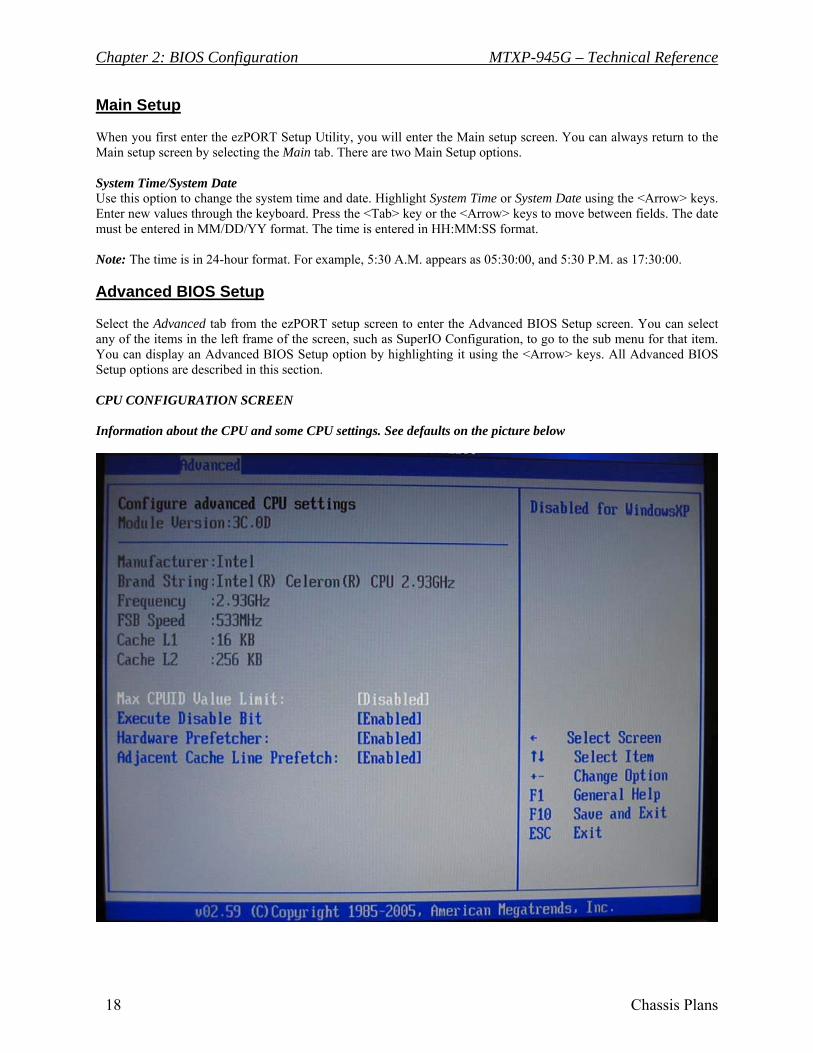
Main Setup When you first enter the ezPORT Setup Utility, you will enter the Main setup screen. You can always return to the Main setup screen by selecting the Main tab. There are two Main Setup options. System Time/System Date Use this option to change the system time and date. Highlight System Time or System Date using the <Arrow> keys. Enter new values through the keyboard. Press the <Tab> key or the <Arrow> keys to move between fields. The date must be entered in MM/DD/YY format. The time is entered in HH:MM:SS format. Note: The time is in 24-hour format. For example, 5:30 A.M. appears as 05:30:00, and 5:30 P.M. as 17:30:00. Advanced BIOS Setup Select the Advanced tab from the ezPORT setup screen to enter the Advanced BIOS Setup screen. You can select any of the items in the left frame of the screen, such as SuperIO Configuration, to go to the sub menu for that item. You can display an Advanced BIOS Setup option by highlighting it using the <Arrow> keys. All Advanced BIOS Setup options are described in this section. CPU CONFIGURATION SCREEN Information about the CPU and some CPU settings. See defaults on the picture below

MTXP-945G Technical Reference Chapter 2:BIOS Configuration
Chassis Plans 19
IDE CONFIGURATION SCREEN IDE Configuration Settings You can use this screen to select options for the IDE Configuration Settings. Use the up and down <Arrow> keys to select an item. Use the <Plus> and <Minus> keys to change the value of the selected option. A description of the selected item appears on the right side of the screen.

Chapter 2: BIOS Configuration MTXP-945G – Technical Reference
20 Chassis Plans
FLOPPY CONFIGURATION SCREEN Floppy Configuration Settings You can use this screen to specify options for the Floppy Configuration Settings. Use the up and down <Arrow> keys to select an item. Use the <Plus> and <Minus> keys to change the value of the selected option. Floppy Drive A: and B: Move the cursor to these fields via up and down <arrow> keys. Select the floppy type. The Optimal setting for floppy drive A: is 1.44 MB 3½”. The Fail-Safe setting for floppy drive A: is 1.44 MB 3½”. The Optimal setting for floppy drive B: is Disabled. The Fail- Safe setting for floppy drive B: is Disabled.
Disabled Set this value to prevent the use of the selected floppy disk drive channel. This option should be set if no floppy disk drive is installed on the specified channel. This is the default setting for Floppy Drive B.
360 KB 5 ¼ ” Set this value if the floppy disk drive attached to the corresponding channel is a 360 KB 5¼ “ floppy disk drive.
1.2 MB 5 ¼ ” Set this value if the floppy disk drive attached to the corresponding channel is a 1.2 MB 5¼ “ floppy disk drive.
720 KB 3 ½ ” Set this value if the floppy disk drive attached to the corresponding channel is a 720 KB 3½ “ floppy disk drive.
1.44 MB 3 ½ ” Set this value if the floppy disk drive attached to the corresponding channel is a 1.44 MB 3½ “ floppy disk drive. This is the default setting for Floppy Drive A.
2.88 MB 3 ½ Set this value if the floppy disk drive attached to the corresponding channel is a 2.88 MB 3½ “ floppy disk drive.

MTXP-945G Technical Reference Chapter 2:BIOS Configuration
Chassis Plans 21
SUPER IO CONFIGURATION SCREEN SuperIO Configuration Screen You can use this screen to select options for the Super I/O settings. Use the up and down <Arrow> keys to select an item. Use the <Plus> and <Minus> keys to change the value of the selected option.
OnBoard Floppy Controller Set this option to Enabled to enable the floppy drive controller on the motherboard. The settings are Enabled and Disabled. The default setting is Enabled. Floppy Disk Control Signals [Internal (FDC)] The Optimal and Fail-Safe default setting is [Internal (FDC)] [Internal (FDC)]
[Parallel (LPT)]

Chapter 2: BIOS Configuration MTXP-945G – Technical Reference
22 Chassis Plans
Serial Port1 Address This option specifies the base I/O port address of serial port 1. The Optimal setting is 3F8. The Fail-Safe default setting is Disabled.
Disabled Set this value to prevent the serial port from accessing any system resources. When this option is set to Disabled, the serial port physically becomes unavailable.
3F8 Set this value to allow the serial port to use 3F8 as its I/O port address. This is the default setting. The majority of serial port 1 or COM1 ports on computer systems use I/O Port 3F8 as the standard setting. The most common serial device connected to this port is a mouse. If the system will not use a serial device, it is best to set this port to Disabled.
2F8 Set this value to allow the serial port to use 2F8 as its I/O port address. If the system will not use a serial device, it is best to set this port to Disabled.
3E8 Set this value to allow the serial port to use 3E8 as its I/O port address. If the system will not use a serial device, it is best to set this port to Disabled.
2E8 Set this value to allow the serial port to use 2E8 as its I/O port address. If the system will not use a serial device, it is best to set this port to Disabled.
Serial Port1 IRQ This option specifies the IRQ of serial port 1. The Optimal setting is 4. This option is not available if serial port1 is disabled.
Options: 3, 4, 10 or 11. Serial Port2 Address [2F8] This option specifies the base I/O port address of serial port 2. The Optimal setting is 2F8. The Fail-Safe default setting is 2F8.
Options: Disabled, 3F8, 2F8, 3E8, 2E8
Serial Port2 IRQ [4] This option specifies the IRQ of serial port 2.. The Optimal and the Fail-safe default setting is 4. This option is not available if serial port2 is disabled.
Options: 3, 4, 10 or 11. Parallel Port Address This option specifies the I/O address used by the parallel port. The Optimal setting is 378. The Fail-Safe setting is Disabled.
Disabled Set this value to prevent the parallel port from accessing any system resources. When the value of this option is set to Disabled, the printer port becomes unavailable.
378 Set this value to allow the parallel port to use 378 as its I/O port address. This is the default setting. The majority of parallel ports on computer systems use IRQ7 and I/O Port 378H as the standard setting.
278 Set this value to allow the parallel port to use 278 as its I/O port address.
3BC Set this value to allow the parallel port to use 3BC as its I/O port address.

MTXP-945G Technical Reference Chapter 2:BIOS Configuration
Chassis Plans 23
Parallel Port Mode This option specifies the parallel port mode. The Optimal setting is Normal. The Fail- Safe setting is Disabled.
Normal Set this value to allow the standard parallel port mode to be used. This is the default setting.
SPP Bi-Dir Set this value to allow data to be sent to and received from the parallel port.
EPP+SPP The parallel port can be used with devices that adhere to the Enhanced Parallel Port (EPP) specification. EPP uses the existing parallel port signals to provide asymmetric bi-directional data transfer driven by the host device.
ECP The parallel port can be used with devices that adhere to the Extended Capabilities Port (ECP) specification. ECP uses the DMA protocol to achieve data transfer rates up to 2.5 Megabits per second. ECP provides symmetric bi-directional communication.
ECP+EPP
Parallel Port IRQ This option specifies the IRQ used by the parallel port. The Optimal and Fail-Safe default setting is 7.
5 Set this value to allow the serial port to use Interrupt 5.
7 Set this value to allow the serial port to use Interrupt 7. This is the default setting. The majority of parallel ports on computer systems use IRQ7 and I/O Port 378h as the standard setting.
Keyboard PowerOn
Disabled, any key, particular key Mouse PowerOn

Chapter 2: BIOS Configuration MTXP-945G – Technical Reference
24 Chassis Plans
HARDWARE HEALTH CONFIGURATION SCREEN Hardware Health Configuration Screen Shows information about temperatures and voltages. Allows control of several environmental functions. The function can be enabled or disabled.

MTXP-945G Technical Reference Chapter 2:BIOS Configuration
Chassis Plans 25
ACPI CONFIGURATION SCREEN ACPI Configuration Screen You can use this screen to select options for the ACPI settings. Use the up and down <Arrow> keys to select an item. Use the <Plus> and <Minus> keys to change the value of the selected option. General ACPI Configuration You can use this screen to select options for the ACPI General Configuration Settings. Use the up and down <Arrow> keys to select an item. Use the <Plus> and <Minus> keys to change the value of the selected option. A description of the selected item appears on the right side of the screen.
Advanced ACPI Configuration You can use this screen to select options for the ACPI Advanced Configuration Settings. Use the up and down <Arrow> keys to select an item. Use the <Plus> and <Minus> keys to change the value of the selected option. A description of the selected item appears on the right side of the screen. ACPI Version Feature Set this value to the desired ACPI specification:
1.0, 2.0, 3.0 ACPI APIC support Include ACPI APIC pointer to RSDT pointer list.

Chapter 2: BIOS Configuration MTXP-945G – Technical Reference
26 Chassis Plans
AMI OEM Table Set this value to allow the ACPI BIOS to add a pointer to an OEMB table in the Root System Description Table (RSDT) table.
Disabled This option disables adding an OEMB table.
Enabled This option enables adding an OEMB table. This is the default setting.
Note: OEMB table is used to pass POST data to the AML code during ACPI O/S operations. RSDT RSDT is the main ACPI table. It has no fixed place in memory. During the boot up process, the BIOS locates a pointer to the table during the memory scan. A Root System Descriptor Pointer (RSDP) is located in low memory space of the system. It provides the physical address of the RSDT. The RSDT itself is identified in memory because it starts with the signature "RSDT." Following the signature is an array of pointers that tell the operating system the location of other description tables that provide it with the information it needs about the standards defined on the current system and individual devices. AML ACPI Machine Language (AML) is a binary code format that the operating system's ACPI AML interpreter parses to discover the machine's properties. On boot up the BIOS startup code copies it into system memory, where it can be interpreted by the operating system’s ACPI AML interpreter. Headless Mode This option is used to update the ACPI FACP table to indicate headless operations.
Disabled This option disables updating the ACPI FACP table to indicate headless operation. This is the default setting.
Enabled This option enables updating the ACPI FACP table to indicate headless operation.
Chipset ACPI Configuration You can use this screen to select options for the Chipset ACPI Configuration Settings. Use the up and down <Arrow> keys to select an item. Use the <Plus> and <Minus> keys to change the value of the selected option. A description of the selected item appears on the right side of the screen. Energy Lake Feature The Optimal and Fail-Safe default setting is Disabled. APIC ACPI SCI IRQ The Optimal and Fail-Safe default setting is Disabled. EVENT LOG CONFIGURATION SCREEN MPS CONFIGURATION SCREEN PCI EXPRESS CONFIGURATION SCREEN SMBIOS CONFIGURATION SCREEN USB CONFIGURATION SCREEN

MTXP-945G Technical Reference Chapter 2:BIOS Configuration
Chassis Plans 27
PCI/PnP Setup Select the PCI/PnP tab from the ezPORT setup screen to enter the Plug and Play BIOS Setup screen. You can display a Plug and Play BIOS Setup option by highlighting it using the <Arrow> keys. Clear NVRAM Set this value to allow the system to clear the NVRAM. The Optimal and Fail-Safe default setting is No. Plug and Play O/S Set this value to allow the system to modify the settings for Plug and Play operating system support. The Optimal and Fail-Safe default setting is Yes.
No The No setting is for operating systems that do not meet the Plug and Play specifications. It allows the BIOS to configure all the devices in the system.
Yes The Yes setting allows the operating system to change the interrupt, I/O, and DMA settings. Set this option if the system is running Plug and Play aware operating systems.
PCI Latency Timer Set this value to allow the PCI Latency Timer to be adjusted. This option sets the latency of all PCI devices on the PCI bus. The Optimal and Fail-Safe default setting is 64 clock cycles.
32, 64, 96, 128, 160, 192, 224, 248 Allocate IRQ to VGA Set this value to allow or restrict the system from giving the VGA adapter card an interrupt address. The Optimal and Fail-Safe default setting is Yes.
Yes Set this value to allow the allocation of an IRQ to a VGA adapter card that uses the PCI local bus. This is the default setting.
No Set this value to prevent the allocation of an IRQ to a VGA adapter card that uses the PCI local bus.
Palette Snooping Set this value to allow the system to modify the Palette Snooping settings. The Optimal and Fail-Safe default setting is Disabled.
Disabled This is the default setting and should not be changed unless the VGA card manufacturer requires Palette Snooping to be Enabled.
Enabled This setting informs the PCI devices that an ISA based Graphics device is installed in the system. It does this so the ISA based Graphics card will function correctly. This does not necessarily indicate a physical ISA adapter card. The graphics chipset can be mounted on a PCI card. Always check with your adapter card’s manuals first, before modifying the default settings in the BIOS.
PCI IDE BusMaster Set this value to allow or prevent the use of PCI IDE bus mastering. The Optimal and Fail-Safe default setting is Disabled.
Disabled Set this value to prevent PCI bus mastering. This is the default setting.
Enabled This option specifies that the IDE controller on the PCI local bus has mastering capabilities.

Chapter 2: BIOS Configuration MTXP-945G – Technical Reference
28 Chassis Plans
OffBoard PCI/ISA IDE Card Set this value to allow the OffBoard PCI/ISA IDE Card to be selected. The Optimal and Fail-Safe default setting is Auto.
Auto This setting will auto select the location of an OffBoard PCI IDE adapter card. This is the default setting.
PCI Slot1 This setting will select PCI Slot 1 as the location of the OffBoard PCI IDE adapter card. Use this setting only if there is an IDE adapter card installed in PCI Slot 1.
PCI Slot2 This setting will select PCI Slot 2 as the location of the OffBoard PCI IDE adapter card. Use this setting only if there is an IDE adapter card installed in PCI Slot 2.
PCI Slot3 PCI Slot4 PCI Slot5 PCI Slot6
IRQ Set this value to allow the IRQ settings to be modified. The Optimal and Fail-Safe default setting is Available.
IRQ3 IRQ4 IRQ5 IRQ7 IRQ9 IRQ10 IRQ11 IRQ14 IRQ15 Available This setting allows the specified IRQ to be used by a PCI/PnP device. This is the default setting. Reserved This setting allows the specified IRQ to be used by a legacy ISA device.
DMA Set this value to allow the DMA setting to be modified. The optimal and Fail-Safe default setting is Available.
DMA Channel 0 DMA Channel 1 DMA Channel 3 DMA Channel 5 DMA Channel 6 DMA Channel 7
Available This setting allows the specified DMA to be used by PCI/PnP device. This is the default setting.
Reserved This setting allows the specified DMA to be used by a legacy ISA device.
Reserved Memory Size Set this value to allow the system to reserve memory that is used by ISA devices. The optimal and Fail-Safe default setting is Disabled.
Disabled Set this value to prevent BIOS from reserving memory to ISA devices.
16K Set this value to allow the system to reserve 16K of the system memory to the ISA devices.
32K Set this value to allow the system to reserve 32K of the system memory to the ISA devices.
64K Set this value to allow the system to reserve 64K of the system memory to the ISA devices.

MTXP-945G Technical Reference Chapter 2:BIOS Configuration
Chassis Plans 29
Reserved Memory Address Note: Reserved Memory Address can be displayed and set manually only if the Reserved Memory
Size is set to 16K, 32K, or 64K. Set this value to the base address of memory block to reserve for legacy ISA devices. The optimal and Fail-Safe default setting is C8000.
C0000 C4000 C8000 CC000 D0000 D4000 D8000 DC000
Boot Setup Select the Boot tab from the ezPORT setup screen to enter the Boot BIOS Setup screen. You can select any of the items in the left frame of the screen, such as Boot Device Priority, to go to the sub menu for that item. You can display a Boot BIOS Setup option by highlighting it using the <Arrow> keys. BOOT SETTINGS CONFIGURATION SCREEN Boot Settings Configuration Use this screen to select options for the Boot Settings Configuration. Use the up and down <Arrow> keys to select an item. Use the <Plus> and <Minus> keys to change the value of the selected option. Quick Boot The Optimal and Fail-Safe default setting is Disabled.
Disabled Set this value to allow the BIOS to perform all POST tests.
Enabled Set this value to allow the BIOS to skip certain POST tests to boot faster.
Quiet Boot Set this value to allow the boot up screen options to be modified between POST messages or OEM logo. The Optimal and Fail-Safe default setting is Enabled.
Disabled Set this value to allow the computer system to display the POST messages.
Enabled Set this value to allow the computer system to display the OEM logo. This is the default setting.
Add-On ROM Display Mode Set this option to display add-on ROM (read-only memory) messages. The Optimal and Fail-Safe default setting is Force BIOS. An example of this is a SCSI BIOS or VGA BIOS.
Force BIOS Set this value to allow the computer system to force a third party BIOS to display during system boot. This is the default setting.
Keep Current Set this value to allow the computer system to display the ezPORT information during system boot.

Chapter 2: BIOS Configuration MTXP-945G – Technical Reference
30 Chassis Plans
Boot up Num-Lock Set this value to allow the Number Lock setting to be modified during boot up. The Optimal and Fail-Safe default setting is On.
Off This option does not enable the keyboard Number Lock automatically. To use the 10-keys on the keyboard, press the Number Lock key located on the upper left-hand corner of the 10-key pad. The Number Lock LED on the keyboard will light up when the Number Lock is engaged.
On Set this value to allow the Number Lock on the keyboard to be enabled automatically when the computer system is boot up. This allows the immediate use of 10-keys numeric keypad located on the right side of the keyboard. To confirm this, the Number Lock LED light on the keyboard will be lit.
PS/2 Mouse Support Set this value to allow the PS/2 mouse support to be adjusted. The Optimal and Fail-Safe default setting is Auto.
Disabled This option will prevent the PS/2 mouse port from using system resources and will prevent the port from being active. Use this setting if installing a serial mouse.
Enabled Set this value to allow the system to use a PS/2 mouse. This is the default setting.
Wait for ‘F1’ If Error Set this value to allow the Wait for ‘F1’ Error setting to be modified. The Optimal and Fail-Safe default setting is Enabled.
Disabled This prevents the ezPORT to wait on an error for user intervention. This setting should be used if there is a known reason for a BIOS error to appear. An example would be a system administrator must remote boot the system. The computer system does not have a keyboard currently attached. If this setting is set, the system will continue to boot up in to the operating system. If ‘F1’ is enabled, the system will wait until the BIOS setup is entered.
Enabled Set this value to allow the system BIOS to wait for any error. If an error is detected, pressing <F1> will enter Setup and the BIOS setting can be adjusted to fix the problem. This normally happens when upgrading the hardware and not setting the BIOS to recognize it. This is the default setting.
Hit ‘DEL’ Message Display Set this value to allow the Hit “DEL” to enter Setup Message Display to be modified. The Optimal and Fail-Safe default setting is Enabled.
Disabled This prevents the ezPORT to display Hit Del to enter Setup
during memory initialization. If Quiet Boot is enabled, the Hit ‘DEL’ message will not display. Enabled This allows the ezPORT to display
Hit Del to enter Setup During memory initialization. This is the default setting.

MTXP-945G Technical Reference Chapter 2:BIOS Configuration
Chassis Plans 31
BOOT DEVICE PRIORITY Boot Device Priority Use this screen to specify the order in which the system checks for the device to boot from. To access this screen, select Boot Device Priority on the Boot Setup screen and press <Enter>.
1st Boot Device 2nd Boot Device 3rd Boot Device
Set the boot device options to determine the sequence in which the computer checks which device to boot from. The settings are Removable Dev., Hard Drive, or ATAPI CDROM. The Optimal and Fail-Safe settings are:
• 1st boot device – Removable Device • 2nd boot device – CD/DVD • 3rd boot device – HDD
To change the boot order, select a boot category type such as Hard disk drives, Removable media, or ATAPI CD ROM devices from the boot menu. For example, if the 1st boot device is set to Hard disk drives, then BIOS will try to boot to hard disk drives first. Note: When you select a boot category from the boot menu, a list of devices in that category appears. For example, if the system has three hard disk drives connected, then the list will show all three hard disk drives attached.

Chapter 2: BIOS Configuration MTXP-945G – Technical Reference
32 Chassis Plans
HARD DISK DRIVES Hard disk drives Use this screen to view the hard disk drives in the system. To access this screen, select Hard disk drives on the Boot Setup screen and press <Enter>. REMOVABLE DEVICES Removable Devices Use this screen to view the removable drives attached to the system. To access this screen, select Removable Devices on the Boot Setup screen and press <Enter>. ATAPI CDROM DRIVES ATAPI CD-ROM Drives Use this screen to view the ATAPI CD-ROM drives in the system. To access this screen, select ATAPI CDROM Drives on the Boot Setup screen and press <Enter>. Security Setup ezPORT Password Support Two Levels of Password Protection ezPORT provides both a Supervisor and a User password. If you use both passwords, the Supervisor password must be set first. The system can be configured so that all users must enter a password every time the system boots or when ezPORT Setup is executed, using either or either the Supervisor password or User password. The Supervisor and User passwords activate two different levels of password security. If you select password support, you are prompted for a one to six character password. Type the password on the keyboard. The password does not appear on the screen when typed. Make sure you write it down. If you forget it, you must drain NVRAM and reconfigure. Remember the Password Keep a record of the new password when the password is changed. If you forget the password, you must erase the system configuration information in NVRAM. See (Deleting a Password) for information about erasing system configuration information. Select Security Setup from the ezPORT Setup main BIOS setup menu. All Security Setup options, such as password protection and virus protection, are described in this section. To access the sub menu for the following items, select the item and press <Enter>:
• Change Supervisor Password • Change User Password • Clear User Password (Note: If the User Password is not installed, the “Clear User Password” will not displayed.)

MTXP-945G Technical Reference Chapter 2:BIOS Configuration
Chassis Plans 33
(Note: If the “Supervisor Password” installed, and the “User Password” not installed, the following will be displayed.)
• Change supervisor Password • User Access Level [Full Access]
The default setting is Full Access.
Options: No Access View Only Limited Full Access
• Change User Password • Password Check [Setup]
The default setting is Setup.
Options: Setup Always
• Boot Sector Virus Protection Supervisor Password Indicates whether a supervisor password has been set. If the password has been installed, Installed displays. If not, Not Installed displays. User Password Indicates whether a user password has been set. If the password has been installed, Installed displays. If not, Not Installed displays. Change Supervisor Password Select this option and press <Enter> to access the sub menu. You can use the sub menu to change the supervisor password. Change User Password Select this option and press <Enter> to access the sub menu. You can use the sub menu to change the user password. Clear User Password Select this option and press <Enter> to access the sub menu. You can use the sub menu to clear the user password. Boot Sector Virus Protection This option is near the bottom of the Security Setup screen. The Optimal and Fail-Safe default setting is Disabled
Disabled Set this value to prevent the Boot Sector Virus Protection. This is the default setting.
Enabled Select Enabled to enable boot sector protection. ezPORT displays a warning when any program (or virus) issues a Disk Format command or attempts to write to the boot sector of the hard disk drive. If enabled, the following appears when a write is attempted to the boot sector. You may have to type N several times to prevent the boot sector write.
Boot Sector Write! Possible VIRUS: Continue (Y/N)? _
The following appears after any attempt to format any cylinder, head, or sector of any hard disk drive via the BIOS INT 13 Hard disk drive Service:
Format!!! Possible VIRUS: Continue (Y/N)? _

Chapter 2: BIOS Configuration MTXP-945G – Technical Reference
34 Chassis Plans
CHANGE SUPERVISOR PASSWORD Change Supervisor Password Select Change Supervisor Password from the Security Setup menu and press <Enter>.
Enter New Password:
appears. Type the password and press <Enter>. The screen does not display the characters entered. Retype the password as prompted and press <Enter>. If the password confirmation is incorrect, an error message appears. The password is stored in NVRAM after ezPORT completes. Change User Password Select Change User Password from the Security Setup menu and press <Enter>.
Enter New Password:
appears. Type the password and press <Enter>. The screen does not display the characters entered. Retype the password as prompted and press <Enter>. If the password confirmation is incorrect, an error message appears. The password is stored in NVRAM after ezPORT completes. Clear User Password Select Clear User Password from the Security Setup menu and press <Enter>.
Clear New Password [Ok] [Cancel]
appears. Type the password and press <Enter>. The screen does not display the characters entered. Retype the password as prompted and press <Enter>. If the password confirmation is incorrect, an error message appears. The password is stored in NVRAM after ezPORT completes. Deleting a Password If you forget the passwords you set up through ezPORT Setup, the only way you can reset the password is to erase the system configuration information where the passwords are stored. System configuration data is stored in CMOS RAM, a type of memory that consumes very little power. You can drain CMOS RAM power by removing the battery or resetting CMOS information using the CMOS erase jumper. Chipset Setup Select the Chipset tab from the ezPORT setup screen to enter the Chipset BIOS Setup screen. You can select any of the items in the left frame of the screen, such as CPU Configuration, to go to the sub menu for that item. You can display a Chipset BIOS Setup option by highlighting it using the <Arrow> keys. All Chipset BIOS Setup options are described in this section.

MTXP-945G Technical Reference Chapter 2:BIOS Configuration
Chassis Plans 35
NORTH BRIDGE CONFIGURATION NorthBridge Configuration You can use this screen to select options for the North Bridge Configuration. Use the up and down <Arrow> keys to select an item. Use the <Plus> and <Minus> keys to change the value of the selected option.
Chapter 2: BIOS Configuration MTXP-945G – Technical Reference
36 Chassis Plans
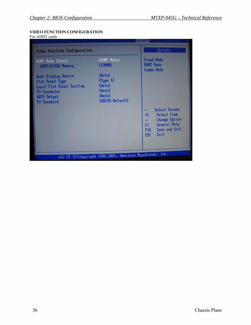
VIDEO FUNCTION CONFIGURATION For ADD2 cards

MTXP-945G Technical Reference Chapter 2:BIOS Configuration
Chassis Plans 37
SOUTH BRIDGE CONFIGURATION
Exit Menu Select the Exit tab from the ezPORT setup screen to enter the Exit BIOS Setup screen. You can display an Exit BIOS Setup option by highlighting it using the <Arrow> keys. All Exit BIOS Setup options are described in this section. Exit Saving Changes When you have completed the system configuration changes, select this option to leave ezPORT Setup and reboot the computer so the new system configuration parameters can take effect. Select Exit Saving Changes from the Exit menu and press <Enter>.
Save Configuration Changes and Exit Now? [Ok] [Cancel]
appears in the window. Select Ok to save changes and exit. Exit Discarding Changes Select this option to quit ezPORT Setup without making any permanent changes to the system configuration. Select Exit Discarding Changes from the Exit menu and press <Enter>.
Discard Changes and Exit Setup Now? [Ok] [Cancel]
appears in the window. Select Ok to discard changes and exit.

Chapter 2: BIOS Configuration MTXP-945G – Technical Reference
38 Chassis Plans
Load Optimal Defaults ezPORT automatically sets all ezPORT Setup options to a complete set of default settings when you Select this option. The Optimal settings are designed for maximum system performance, but may not work best for all computer applications. In particular, do not use the Optimal ezPORT Setup options if your computer is experiencing system configuration problems.
Select Load Optimal Defaults from the Exit menu and press <Enter>. Select Ok to load optimal defaults.
Load Fail-Safe Defaults ezPORT automatically sets all ezPORT Setup options to a complete set of default settings when you Select this option. The Fail-Safe settings are designed for maximum system stability, but not maximum performance. Select the Fail-Safe ezPORT Setup options if your computer is experiencing system configuration problems. Select Load Fail-Safe Defaults from the Exit menu and press <Enter>.
Load Fail-Safe Defaults? [Ok] [Cancel]
appears in the window. Select Ok to load Fail-Safe defaults. Discard Changes Select Discard Changes from the Exit menu and press <Enter>.
Select Ok to discard changes.

MTXP-945G Technical Reference_____________________ Chapter 3: Upgrading
Chassis Plans 39
Chapter 3 Upgrading
Upgrading the Microprocessor The latest revision of the MTXP-945G currently supports Intel Pentium 4 processors in an LGA775 processor socket with a 1066, 800, or 533 MHz system bus. Use Only ATX12V compliant power supplies. A good CPU cooling FAN must be used and use a plastic cooler back plate when installing the fan cooler assembly on to the CPU. Upgrading the System Memory The MTXP-945G supports the following memory features:
• 1.8 V (only) DDR2 SDRAM DIMMs with gold-plated contacts. • Unbuffered, single-sided or double-sided DIMMs with the following restriction: • Double-sided DIMMS with x16 organization are not supported. • 4 GB maximum total system memory. • Minimum total system memory: 128 MB • Non-ECC DIMMs • Serial Presence Detect • DDR2 667, DDR2 533, or DDR2 400 MHz SDRAM DIMMs
The following table lists the supported DDR DIMM Configurations:
Table 3-1 Supported DDR SODIMM Configurations
Front Side Population
Back Side Population
DIMM Capacity
# of Dev./ DIMM
# of Sides
DRAM Tech.
Count Config Count Config
128 MB 4 SS 256 Mbit
4 16 M x 16
256 MB 8 SS 256 Mbit
8 32 M x 8
256 MB 4 SS 512 Mbit
4 32 M x 16
512 MB 16 DS 256 Mbit
8 32 M x 8
8 32 M x 8
512 MB 8 SS 512 Mbit
8 64 M x 8
512 MB 4 SS 1 Gbit 4 64 M x 16
1024 MB 16 DS 512 Mbit
8 64 M x 8
8 64 M x 8
1024 MB 8 SS 1 Gbit 8 128 M x 8
2048 MB 16 DS 1 Gbit 8 128 M x 8
8 128 M x 8

Chapter 3: Upgrading MTXP-945G Technical Reference
40 Chassis Plans
The MTXP-945G supports two types of memory organization: Dual channel (Interleaved) mode. This mode offers the highest throughput for real world applications. Dual channel mode is enabled when the installed memory capacities of both DIMM channels are equal. Technology and device width can vary from one channel to the other but the installed memory capacity for each channel must be equal. If different speed DIMMs are used between channels, the slowest memory timing will be used. Single channel (Asymmetric) mode. This mode is equivalent to single channel bandwidth operation for real world applications. This mode is used when only a single DIMM is installed or the memory capacities are unequal. Technology and device width can vary from one channel to the other. If different speed DIMMs are used between channels, the slowest memory timing will be used.

MTXP-945G Technical Reference Appendix A: Technical Specifications
Chassis Plans 41
Appendix A Technical Specifications Chipsets Core Logic
North Bridge - Intel 945G. South Bridge – Intel ICH7R.
Peripheral I/O Standard Microsystems (SMSC) SCH311x.
BIOS System BIOS
American Megatrends AMIBIOS.
Flash BIOS Standard feature for System BIOS. Flash programming built into the BIOS. BIOS to be flashed is read from a floppy.
Embedded I/O Floppy
2 Floppies up to 2.88 MB.
IDE Single channel PCI 32-bit EIDE controller – UDMA 66/100 supported. One Standard 40-pin and one mini-Header 44 pin for Solid State IDE disk or any 44 pin IDE device support.
Parallel ATA IDE Interfaces The ICH4 Parallel ATA IDE controller has one independent bus-mastering Parallel ATA IDE interface that can be enabled. The Parallel ATA IDE interface supports the following modes:
• Programmed I/O (PIO): processor controls data transfer. • 8237-style DMA: DMA offloads the processor, supporting transfer rates of up to 16 MB/sec. • Ultra DMA: DMA protocol on IDE bus supporting host and target throttling and transfer rates of
up to 33 MB/sec. • ATA-66: DMA protocol on IDE bus supporting host and target throttling and transfer rates of up
to 66 MB/sec. ATA-66 protocol is similar to Ultra DMA and is device driver compatible. • ATA-100: DMA protocol on IDE bus allows host and target throttling. The ICH ATA-100 logic
can achieve read transfer rates up to 100 MB/sec and write transfer rates up to 88 MB/sec. NOTE ATA-66 and ATA-100 are faster timings and require a specialized cable (80-conductor) to reduce reflections, noise, and inductive coupling. The Parallel ATA IDE interface also support ATAPI devices (such as CD-ROM drives). The BIOS supports Logical Block Addressing (LBA) and Extended Cylinder Head Sector (ECHS) translation modes. The drive reports the transfer rate and translation mode to the BIOS. The MTXP-945G supports Laser Servo (LS-120) diskette technology through the Parallel ATA IDE interface. The BIOS supports booting from an LS-120 drive.

Appendix A: Technical Specifications MTXP-945G – Technical Reference
42 Chassis Plans
NOTE The BIOS will always recognize an LS-120 drive as an ATAPI floppy drive. To ensure correct operation, do not configure the drive as a hard disk drive. Serial ATA Interfaces The MTXP-945G features four independent Serial ATA ports with a theoretical maximum transfer rate of 300 MB/s per port. One device can be installed on each port for a maximum of four Serial ATA devices. A point-to-point interface is used for host to device connections, unlike Parallel IDE, which supports a master/slave configuration and two devices per channel. For compatibility, the underlying Serial ATA functionality is transparent to the operating system. NOTE Many Serial ATA drives use new low-voltage power connectors and require adaptors or power supplies equipped with low-voltage power connectors.
Serial Ports Up to six high speed RS-232 serial ports 16 Bytes FIFO (16550/16550D). COM2 optional RS-232 IrDA and COM1 optional RS-422/485. COM1 and COM2 are standard, other ports are optional.
Parallel Port One bi-directional parallel port. EPP/ECP mode compatible.
Keyboard/Mouse Port One mouse/keyboard combined PS/2 connector
USB Interfaces
Eight Universal Serial Bus connectors. USB 1.1 and USB 2.0 compliant. On-board Ethernet
One (optional two) PCI Express based Gigabit Ethernet controllers (Intel 82573L).
On-board Buzzer
Audio Intel HD Audio. Microphone In, Stereo Line In and Out, Aux In and CD In.
Industrial Devices Temperature and Voltage Device
Automatic CPU voltage & temperature monitoring device embedded on the peripheral I/O controller. Power Management
Power button function: advanced power management support.
Post Code Display

MTXP-945G Technical Reference Appendix A: Technical Specifications
Chassis Plans 43
Miscellaneous CMOS/Battery
RTC with lithium battery.
Control Panel Connections Reset, Soft Power. LEDs for power and IDE.
CPU Socket LGA775 socket.
Form Factor Micro-ATX form factor - 24.5x24.5 cm (9.6 x 9.6 inches)
PCB Construction Four Layers, dry film mask.
Manufacturing Process
Automated surface mount.
Table A-1 Environmental Specifications
Environmental Operating Non-operating Temperature 0° to +60° C -40° to +65° C
Humidity 5 to 95% @ 40° C non-condensing
5 to 95% @ 40° C non-condensing
Shock 2.5G @ 10ms 10G @ 10ms Vibration 0.25 @ 5-100Hz 5 @ 5-100Hz

Appendix A: Technical Specifications MTXP-945G – Technical Reference
44 Chassis Plans
Mechanical Drawing

MTXP-945G Technical Reference Appendix A: Technical Specifications
Chassis Plans 45
Memory Map Address Range Decimal Address Range
Hexadecimal Size Description
960K-1M 0F0000-0FFFFF 64 KB Upper BIOS 896K-960K 0E0000-0EFFFF 64 KB Lower BIOS
768K-896K 0C0000-0DFFFF 128 KB Expansion Card BIOS and Buffer
640K-768K 0A0000-0BFFFF 128 KB Standard PCI/ISA Video Memory
633K-640K 09E400-09FFFF 7KB BIOS Reserved
512K-633K 080000-09E3FF 121 KB Ext. Conventional memory
0K- 512K 000000-07FFFF 512 KB Conventional memory DMA Channels DMA # Data Width System Resource 0 8- or 16-bits 1 8- or 16-bits Parallel port (for ECP) (if selected) 2 8- or 16-bits Floppy Drive 3 8- or 16-bits Parallel port (for ECP) (if selected) 4 Reserved- cascade channel 5 16-bits Open 6 16-bits Open 7 16-bits Open
I/O Map Address (hex) Description 0000-000F DMA 1 0020-0021 Interrupt Controller 1 0040 Timer/Counter 0 0041 Timer/Counter 1 0042 Timer/Counter 2 0043 Timer Control Word 0060 Keyboard Controller Byte _ Reset IRQ 0061 NMI Status and Control 0070, bit 7 NMI enable 0070, bits 6:0 RTC Index 0071 RTC Data 0072 RTC Extended Index 0073 RTC Extended Data 0080-008F DMA page registers / POST code display also located at 0080h 0092 Port 92 00A0-00A1 Interrupt Controller 2 00B2-00B3 APM control

Appendix A: Technical Specifications MTXP-945G – Technical Reference
46 Chassis Plans
Address (hex) Description 00C0-00DE DMA 2 00F0 Coprocessor Error 0170 _ 0177 Secondary IDE channel 01F0 _ 01F7 Primary IDE channel 0278-027F LPT2 (if selected) 02E8-02EF COM4 (default) 02F8-02FF COM2 (default) 0376 Secondary IDE channel command port 0377 Floppy channel 2 command 0377, bit 7 Floppy disk change, channel 2 0377, bits 6:0 Secondary IDE channel status port 0378-037F LPT1 (default) 03B4-03B5 Video (VGA) 03BA Video (VGA) 03BC-03CD LPT3 (if selected) 03C0-03CA Video (VGA) 03CC Video (VGA) 03CE-03CF Video (VGA) 03D4-03D5 Video (VGA) 03DA Video (VGA) 03E8-03EF COM3 (default) 03F0-03F5 Floppy Channel 1 03F6 Primary IDE channel command port 03F7 Floppy Channel 1 command 03F7, bit 7 Floppy disk change channel 1 03F7, bits 6:0 Primary IDE channel status report 03F8-03FF COM1 (default) 0CF8-0CFB - 4 bytes PCI configuration address register 0CF9 Reset control register 0CFC-0CFF - 4 bytes PCI configuration data register
Interrupts IRQ System Resource NMI I/O channel check 0 Reserved, interval timer 1 Reserved (keyboard) 2 Reserved (cascade) 3 COM2* 4 COM1* 5 User Available for PCI 6 Floppy Drive 7 LPT1* 8 Real time clock 9 User Available for PCI 10 User Available for PCI 11 User Available for PCI 12 PS/2 mouse port 13 Reserved (math coprocessor) 14 Primary IDE 15 Secondary IDE *Default, but can be changed to another IRQ
MTXP-945G Technical Reference Appendix A: Technical Specifications
Chassis Plans 47
SMBUS
Device Slave Address SIO 00101101b DIMM0 01010000b DIMM1 01010001b DIMM2 01010010b DIMM3 01010011b Clock Chip Write 11010010b Clock Chip Read 11010011b
PCI Interrupt Routing Map PCI Device ID SEL PIRQA PIRQB PIRQC PIRQD PIRQE PIRQF PIRQG PIRQH PCI Slot1 AD17 INTA INTB INTC INTD PCI Slot2 AD18 INTB INTC INTD INTA
Connectors Pin-out
How to identify pin number 1: Looking to the solder side (The board side with fewer components) of the PCB (Printed Circuit Board), pin number 1 will have a squared pad . Other pins will have a circular pad .
How to identify other pins: Connectors type DB, PS/2, AT, RJ45, Power ATX and USB are industry standards. DB connectors, for instance, are numbered sequentially. The first row is numbered in sequence (be aware that male and female connectors are mirrored – male connectors are numbered from left to right when viewed from front and female connectors are numbered from right to left when viewed from front). The following rows resume the counting on the same side of pin number 1. The counting is NOT circular like Integrated Circuits (legacy from electronic tubes).
Header connectors are numbered alternately, i.e. pin number 2 is in the other row, but in the same column of pin number 1. Pin number 3 is in the same row of pin 1, but in the next column and so forth.
Table A-9 Serial Port COM1 DB9 Connector J4A
Pin# Serial Port COM 1 – J4A 1 DCD - RS-422/485RXB(opt.) 2 RX - RS-422/485TXB(opt.) 3 TX - RS-422/485TXA(opt.) 4 DTR 5 GND 6 DSR 7 RTS 8 CTS 9 RI – RS-422/485RXA(opt.)
1 2 3 4 5 6 7 8 9
5 4 3 2 1 9 8 7 6
DB9 Male Front view
DB9 FemaleFront view
1 3 5 7 9 2 4 6 8 10
Header 10 pin connector View from solder side of the PCB

Appendix A: Technical Specifications MTXP-945G – Technical Reference
48 Chassis Plans
Table A-10 Serial Port COM2 DB9 Connector J4B
Pin# Serial Port COM 2 – J4B 1 DCD 2 RX 3 TX 4 DTR 5 GND 6 DSR 7 RTS 8 CTS 9 RI

MTXP-945G Technical Reference Appendix A: Technical Specifications
Chassis Plans 49
Table A-11 Serial Port COM3-6 Header Connector J2 (Optional)
Pin# Serial Port COM 3-6 Header – J2
1 DCD3 2 DSR3 3 RX3 4 RTS3 5 TX3 6 CTS3 7 DTR3 8 RI3 9 GND
10 NC 11 DCD4 12 DSR4 13 RX4 14 RTS4 15 TX4 16 CTS4 17 DTR4 18 RI4 19 GND 20 NC 21 NC 22 NC 23 RX5 24 RTS5 25 TX5 26 CTS5 27 NC 28 NC 29 GND 30 NC 31 NC 32 NC 33 RX6 34 RTS6 35 TX6 36 CTS6 37 NC 38 NC 39 GND 40 NC

Appendix A: Technical Specifications MTXP-945G – Technical Reference
50 Chassis Plans
Table A-12 J41 Ethernet Header
Pin# Ethernet Header Connector – J41 1 2.25V STDBY 2 GND 3 MDI +0 4 MDI -0 5 MDI +1 6 MDI -1 7 MDI +2 8 MDI -2 9 MDI +3 10 MDI -3
Table A-13 J16 USB Ports 0 & 1 Header Connector
Pin# USB Header – J16 1 +5V – USB0 2 +5V – USB1 3 -D – USB0 4 -D – USB1 5 +D – USB0 6 +D – USB1 7 GROUND – USB0 8 GROUND – USB1 9 NC
10 Over Current
Table A-14 J17 USB Ports 2 & 3 Header Connector
Pin# USB Header – J17 1 +5V – USB2 2 +5V – USB3 3 -D – USB2 4 -D – USB3 5 +D – USB2 6 +D – USB3 7 GROUND – USB2 8 GROUND – USB3 9 NC
10 Over Current

MTXP-945G Technical Reference Appendix A: Technical Specifications
Chassis Plans 51
Table A-15 J19 SPI Header Connector
Pin# SPI Header – J19 1 VCC 2 GND 3 CS 4 CLK 5 MOSO 6 MOSI
Table A-16 J7 Front Panel Header Connector
Pin# Front Panel Header – J7 1 HDD LED Anode 2 Power LED Green Blink 3 HDD LED Cathode 4 Power LED Yellow Blink 5 Reset - GND 6 Power Switch 7 Reset 8 Power Switch - GND 9 +5V 10 NC
Table A-17 J15 IrDA Connector
Pin# IrDA– J15 1 Infra Red Rx (Opt.) 2 GND 3 GND 4 NC 5 Infra Red Tx (Opt.) 6 +5VDC

Appendix A: Technical Specifications MTXP-945G – Technical Reference
52 Chassis Plans
Table A18 J1 Parallel Header Connector
Pin# Parallel Header – J1 1 -STROBE 2 AUTOFEED 3 +DATA BIT 0 4 ERROR 5 +DATA BIT 1 6 INIT 7 +DATA BIT 2 8 SLCT IN 9 +DATA BIT 3
10 GND 11 +DATA BIT 4 12 GND 13 +DATA BIT 5 14 GND 15 +DATA BIT 6 16 GND 17 +DATA BIT 7 18 GND 19 ACK1 20 GND 21 BUSY 22 GND 23 PAPER EMPTY 24 GND 25 SLCT 26 NC
Table A-19 J12 Audio Microphone In, Line Out/Headphone Out Header Connector
Pin# Audio Header – J12 1 Mic2 Left 2 Audio GND 3 Mic2 Right 4 Audio JD 5 Line OUT R 6 Pull Down 7 Sense 8 NC 9 Line OUT L 10 Pull Down

MTXP-945G Technical Reference Appendix A: Technical Specifications
Chassis Plans 53
Table A-20 CPU Fan, Sys Fan1, Sys Fan2, Ext Temp, RIWAKE, CD IN and Aux IN.
Connector Description CPU FAN J38 1) GND 2)+12V 3) Sense 4) PWM
Sys FAN1 J39 1) GND (PWM) 2)+12V 3) Sense
Sys FAN2 J18 1) GND (PWM) 2)+12V 3) Sense
External Temperature J3 1) Temp In 2) Temp Gnd
RIWAKE J20 1) VCC 2) GND 3) PME
CD IN J13 1)Left 2)GND 3)GND 4)Right
AUX IN J14 1) Left 2)GND 3)GND 4) Right
User's Notes:

Appendix A: Technical Specifications MTXP-945G – Technical Reference
54 Chassis Plans
This page intentionally blank

MTXP-945G Technical Reference Appendix B: Flash BIOS
Chassis Plans 55
BIOS Programming Warning:
Never turn the power off while reprogramming a Flash Bios.
Doing so may make the board unusable and require a return to Chassis Plans to reinitialize the BIOS chip.
Appendix B Flash BIOS programming and codes The MTXP-945G offers the standard FLASH BIOS. When installed, you will be able to update your BIOS without having to replace the EEPROM. The AMIBIOS will read the new BIOS file from a floppy disk during boot and replace the old BIOS.
When updating your BIOS, make sure you have a disk with the correct BIOS file (its size should be 4Mb (512kB)) named AMIBOOT.ROM.
How to reflash the BIOS:
• Insert a floppy containing AMIBOOT.ROM into floppy A: • Press [ctrl][home] during the beginning of POST(boot). • Wait for the procedure to finish and reboot.

Appendix B: Flash BIOS MTXP-945G Technical Reference
56 Chassis Plans
Troubleshooting POST
AMIBIOS writes progress codes, also known as POST codes, to I/O port 80h during POST, in order to provide information to OEM developers about system faults. These POST codes may be monitored by the On-board POST Display.
Table B-1 Bootblock Initialization Code Checkpoints
The Bootblock initialization code sets up the chipset, memory and other components before system memory is available. The following table describes the type of checkpoints that may occur during the bootblock initialization portion of the BIOS.
Checkpoint Code Description Before D1 Early chipset initialization is done. Early super I/O initialization is done including RTC and
keyboard controller. NMI is disabled. D1 Perform keyboard controller BAT test. Check if waking up from power management
suspend state. Save power-on CPUID value in scratch CMOS. D0 Go to flat mode with 4GB limit and GA20 enabled. Verify the bootblock checksum. D2 Disable CACHE before memory detection. Execute full memory sizing module. Verify that
flat mode is enabled. D3 If memory sizing module not executed, start memory refresh and do memory sizing in
Bootblock code. Do additional chipset initialization. Re-enable CACHE. Verify that flat mode is enabled.
D4 Test base 512KB memory. Adjust policies and cache first 8MB. Set stack. D5 Bootblock code is copied from ROM to lower system memory and control is given to it.
BIOS now executes out of RAM. D6 Both key sequence and OEM specific method is checked to determine if BIOS recovery is
forced. Main BIOS checksum is tested. If BIOS recovery is necessary, control flows to checkpoint E0. See Bootblock Recovery Code Checkpoints section of document for more information.
D7 Restore CPUID value back into register. The Bootblock-Runtime interface module is moved to system memory and control is given to it. Determine whether to execute serial flash.
D8 The Runtime module is uncompressed into memory. CPUID information is stored in memory.
D9 Store the Uncompressed pointer for future use in PMM. Copying Main BIOS into memory. Leaves all RAM below 1MB Read-Write including E000 and F000 shadow areas but closing SMRAM.
DA Restore CPUID value back into register. Give control to BIOS POST (ExecutePOSTKernel). See POST Code Checkpoints section of document for more information.
E1-E8 EC-EE OEM memory detection/configuration error. This range is reserved for chipset vendors & system manufacturers.

MTXP-945G Technical Reference Appendix B: Flash BIOS
Chassis Plans 57
Table B-2 Bootblock Recovery Code Checkpoints
The Bootblock recovery code gets control when the BIOS determines that a BIOS recovery needs to occur because the user has forced the update or the BIOS checksum is corrupt. The following table describes the type of checkpoints that may occur during the Bootblock recovery portion of the BIOS:
Checkpoint Code Description E0 Initialize the floppy controller in the super I/O. Some interrupt vectors are initialized. DMA
controller is initialized. 8259 interrupt controller is initialized. L1 cache is enabled. E9 Set up floppy controller and data. Attempt to read from floppy. EA Enable ATAPI hardware. Attempt to read from ARMD and ATAPI CDROM. EB Disable ATAPI hardware. Jump back to checkpoint E9. EF Read error occurred on media. Jump back to checkpoint EB. F0 Search for pre-defined recovery file name in root directory. F1 Recovery file not found. F2 Start reading FAT table and analyze FAT to find the clusters occupied by the recovery file. E0 Initialize the floppy controller in the super I/O. Some interrupt vectors are initialized. DMA
controller is initialized. 8259 interrupt controller is initialized. L1 cache is enabled. E9 Set up floppy controller and data. Attempt to read from floppy. EA Enable ATAPI hardware. Attempt to read from ARMD and ATAPI CDROM. EB Disable ATAPI hardware. Jump back to checkpoint E9. EF Read error occurred on media. Jump back to checkpoint EB. F0 Search for pre-defined recovery file name in root directory. F1 Recovery file not found. F2 Start reading FAT table and analyze FAT to find the clusters occupied by the recovery file.

Appendix B: Flash BIOS MTXP-945G Technical Reference
58 Chassis Plans
Table B-3 POST Code Checkpoints
The POST code checkpoints are the largest set of checkpoints during the BIOS pre-boot process. The following table describes the type of checkpoints that may occur during the POST portion of the BIOS:
Checkpoint Code Description 03 Disable NMI, Parity, video for EGA, and DMA controllers. Initialize BIOS, POST,
Runtime data area. Also initialize BIOS modules on POST entry and GPNV area. Initialized CMOS as mentioned in the Kernel Variable "wCMOSFlags."
04 Check CMOS diagnostic byte to determine if battery power is OK and CMOS checksum is OK. Verify CMOS checksum manually by reading storage area. If the CMOS checksum is bad, update CMOS with power-on default values and clear passwords. Initialize status register A. Initializes data variables that are based on CMOS setup questions. Initializes both the 8259 compatible PICs in the system
05 Initializes the interrupt controlling hardware (generally PIC) and interrupt vector table. 06 Do R/W test to CH-2 count reg. Initialize CH-0 as system timer. Install the POSTINT1Ch
handler. Enable IRQ-0 in PIC for system timer interrupt. Traps INT1Ch vector to "POSTINT1ChHandlerBlock."
C0 Early CPU Init Start -- Disable Cache - Init Local APIC C1 Set up boot strap processor Information C2 Set up boot strap processor for POST C5 Enumerate and set up application processors C6 Re-enable cache for boot strap processor C7 Early CPU Init Exit 0A Initializes the 8042 compatible Key Board Controller. 0B Detects the presence of PS/2 mouse. 0C Detects the presence of Keyboard in KBC port. 0E Testing and initialization of different Input Devices. Also, update the Kernel Variables.
Traps the INT09h vector, so that the POST INT09h handler gets control for IRQ1. Uncompress all available language, BIOS logo, and Silent logo modules.
13 Early POST initialization of chipset registers. 24 Uncompress and initialize any platform specific BIOS modules. 30 Initialize System Management Interrupt. 2A Initializes different devices through DIM.
See DIM Code Checkpoints section of document for more information. 2C Initializes different devices. Detects and initializes the video adapter installed in the system
that have optional ROMs. 2E Initializes all the output devices. 31 Allocate memory for ADM module and uncompress it. Give control to ADM module for
initialization. Initialize language and font modules for ADM. Activate ADM module. 33 Initializes the silent boot module. Set the window for displaying text information. 37 Displaying sign-on message, CPU information, setup key message, and any OEM specific
information. 38 Initializes different devices through DIM. See DIM Code Checkpoints section of document
for more information. 39 Initializes DMAC-1 & DMAC-2. 3A Initialize RTC date/time. 3B Test for total memory installed in the system. Also, Check for DEL or ESC keys to limit
memory test. Display total memory in the system. 3C Mid POST initialization of chipset registers. 40 Detect different devices (Parallel ports, serial ports, and coprocessor in CPU, … etc.)
successfully installed in the system and update the BDA, EBDA…etc.

MTXP-945G Technical Reference Appendix B: Flash BIOS
Chassis Plans 59
50 Programming the memory hole or any kind of implementation that needs an adjustment in system RAM size if needed.
52 Updates CMOS memory size from memory found in memory test. Allocates memory for Extended BIOS Data Area from base memory.
60 Initializes NUM-LOCK status and programs the KBD typematic rate. 75 Initialize Int-13 and prepare for IPL detection. 78 Initializes IPL devices controlled by BIOS and option ROMs. 7A Initializes remaining option ROMs. 7C Generate and write contents of ESCD in NVRam. 84 Log errors encountered during POST. 85 Display errors to the user and gets the user response for error. 87 Execute BIOS setup if needed / requested. 8C Late POST initialization of chipset registers. 8D Build ACPI tables (if ACPI is supported) 8E Program the peripheral parameters. Enable/Disable NMI as selected 90 Late POST initialization of system management interrupt. A0 Check boot password if installed. A1 Clean-up work needed before booting to OS. A2 Takes care of runtime image preparation for different BIOS modules. Fill the free area in
F000h segment with 0FFh. Initializes the Microsoft IRQ Routing Table. Prepares the runtime language module. Disables the system configuration display if needed.
A4 Initialize runtime language module. A7 Displays the system configuration screen if enabled. Initialize the CPU’s before boot, which
includes the programming of the MTRR’s. A8 Prepare CPU for OS boot including final MTRR values. A9 Wait for user input at config display if needed. AA Uninstall POST INT1Ch vector and INT09h vector. Deinitializes the ADM module. AB Prepare BBS for Int 19 boot. AC End of POST initialization of chipset registers. B1 Save system context for ACPI. 00 Passes control to OS Loader (typically INT19h). 61-70 OEM POST Error. Table B-4 DIM Code Checkpoints
The Device Initialization Manager (DIM) gets control at various times during BIOS POST to initialize different system busses. The following table describes the main checkpoints where the DIM module is accessed:
Checkpoint Code Description 2A Initialize different buses and perform the following functions: Reset, Detect, and Disable
(function 0); Static Device Initialization (function 1); Boot Output Device Initialization (function 2). Function 0 disables all device nodes, PCI devices, and PnP ISA cards. It also assigns PCI bus numbers. Function 1 initializes all static devices that include manual configured onboard peripherals, memory and I/O decode windows in PCI-PCI bridges, and noncompliant PCI devices. Static resources are also reserved. Function 2 searches for and initializes any PnP, PCI, or AGP video devices.
38 Initialize different buses and perform the following functions: Boot Input Device Initialization (function 3); IPL Device Initialization (function 4); General Device Initialization (function 5). Function 3 searches for and configures PCI input devices and detects if system has standard keyboard controller. Function 4 searches for and configures all PnP and PCI boot devices. Function 5 configures all onboard peripherals that are set to an automatic configuration and configures all remaining PnP and PCI devices.

Appendix B: Flash BIOS MTXP-945G Technical Reference
60 Chassis Plans
While control is in the different functions, additional checkpoints are output to port 80h as a word value to identify the routines under execution. The low byte value indicates the main POST Code Checkpoint. The high byte is divided into two nibbles and contains two fields. The details of the high byte of these checkpoints are as follows: HIGH BYTE XY The upper nibble 'X' indicates the function number that is being executed. 'X' can be from 0 to 7.
0 = func#0, disable all devices on the BUS concerned. 1 = func#1, static devices initialization on the BUS concerned. 2 = func#2, output device initialization on the BUS concerned. 3 = func#3, input device initialization on the BUS concerned. 4 = func#4, IPL device initialization on the BUS concerned. 5 = func#5, general device initialization on the BUS concerned. 6 = func#6, error reporting for the BUS concerned. 7 = func#7, add-on ROM initialization for all BUSes. 8 = func#8, BBS ROM initialization for all BUSes.
The lower nibble 'Y' indicates the BUS on which the different routines are being executed. 'Y' can be from 0 to 5.
0 = Generic DIM (Device Initialization Manager). 1 = On-board System devices. 2 = ISA devices. 3 = EISA devices. 4 = ISA PnP devices. 5 = PCI devices.
Table B-5 ACPI Runtime Checkpoints
ACPI checkpoints are displayed when an ACPI capable operating system either enters or leaves a sleep state. The following table describes the type of checkpoints that may occur during ACPI sleep or wake events:
Checkpoint Code Description AC First ASL check point. Indicates the system is running in ACPI mode. AA System is running in APIC mode. 01, 02, 03, 04, 05 Entering sleep state S1, S2, S3, S4, or S5. 10, 20, 30, 40, 50 Waking from sleep state S1, S2, S3, S4, or S5. Critical Error BEEP Codes The following table describes the beep codes that are used by AMIBIOS: Table B-6 AMIBIOS Beep Codes
Number of Beeps Description 1 Memory refresh timer error. 2 Parity error 3 Main memory read / write test error. 4 Motherboard timer not operational 5 Processor error 6 Keyboard controller BAT test error. 7 General exception error. 8 Display memory error. 9 ROM checksum error 10 CMOS shutdown register read/write error 11 Cache memory bad

MTXP-945G Technical Reference Appendix B: Flash BIOS
Chassis Plans 61
User's Notes:

Appendix B: Flash BIOS MTXP-945G Technical Reference
62 Chassis Plans
This page intentionally blank

MTXP-945G Technical Reference Appendix C: Industrial Devices
Chassis Plans 63
Appendix C On-Board Industrial Devices The MTXP-945G offers one or two Gigabit Ethernet controller and up to six serial ports (one optional RS422/485). The MTXP-945G also offers three other On-Board Industrial devices: Watchdog timer, Hardware health monitor and a Post Code display that will help you on troubleshooting.
Post Code Display
The POST code display is a device implemented on the MTXP-945G to help on failure diagnostics. A POST code is transmitted by the BIOS during the POST (Power On Self Test). It is a number that refers to the state or test condition of a circuit or group of circuits. Knowing the results of these tests (hence the POST code) can be very important in debugging a system.
POST Checkpoint Codes
When AMIBIOS performs the Power On Self Test, it writes diagnostic codes checkpoint codes to I/O port 0080h where the POST code display is connected. Please, refer to Appendix B for POST codes description.
On-board Ethernet
The MTXP-945G features one or optionally two Gigabit Ethernet controllers. The Ethernet controller is an Intel 82573L.
PCIe — x1 PCIe interface — Peak bandwidth: 2 Gb/s per direction — Power management — High bandwidth density per pin MAC — Optimized transmit and receive queues — IEEE 802.3x compliant flow control with software controlled pause times and threshold values — Caches up to 64 packet descriptors per queue — Programmable host memory receive buffers (256 bytes to 16 KB) and cache line size (16 bytes to 256 bytes) — 32 KB configurable transmit and receive FIFO buffer — Mechanism available for reducing interrupts generated by transmit and receive operation — Descriptor ring management hardware for transmit and receive — Optimized descriptor fetching and write-back mechanisms — Wide, pipelined internal data path architecture PHY — Integrated PHY for 10/100/1000 Mb/s full and half duplex operation — IEEE 802.3ab auto negotiation support — IEEE 802.3ab PHY compliance and compatibility — DSP architecture implements digital adaptive equalization, echo cancellation, and cross-talk cancellation Host Offloading — Transmit and receive IP, TCP and UDP checksum off-loading capabilities — Transmit TCP segmentation, IPv6 offloading, and advanced packet filtering — IEEE 802.1q VLAN support with VLAN tag insertion, stripping and packet filtering for up to 4096 VLAN tags — Descriptor ring management hardware for transmit and receive

Appendix C: Industrial Devices MTXP-945G Technical Reference
64 Chassis Plans
Serial Ports
The MTXP-945G can be configured with up to six fixed RS-232 serial ports (COM1 RS-422/485 optional). COM1 and COM2 are standard, the others are optional.
TIA/EIA-232
RS is the abbreviation for recommended standard. Usually, it is based on or is identical to other standards, e.g., EIA/TIA-232-F. TIA/EIA-232, previously known as RS-232 was developed in the 1960’s to interconnect layers of the interface (ITU–T V.11), but also the pignut of the appropriate connectors (25-pin D-type or 9-pin DB9S) (ISO 2210) and the protocol (ISSUED-T V.24). The interface standard specifies also handshake and control lines in addition to the 2 unidirectional receive data line (RD) and transmit data line (TD). The control lines data carrier detect (DCD), data set ready (DSR), request to send (RTS), clear to send (CTS), data terminal ready (DTR), and the ring indicator (RI) might be used, but do not necessarily have to be (for example, the PC-serial-mouse utilizes only RI, TD, RD and GND). Although the standard supports only low speed data rates and line length of approximately 20 m maximum, it is still widely used. This is due to its simplicity and low cost.
Electrical
TIA/EIA-232 has high signal amplitudes of ±(5 V to 15 V) at the driver output. The triggering of the receiver depends on the sign of the input voltage: that is, it senses whether the input is above 3 V or less than –3 V. The line length is limited by the allowable capacitive load of less than 2500 pF. This results in a line length of approximately 20 m. The maximum slope of the signal is limited to 30 V/ms. The intention here is to limit any reflections that can occur to the rise-and fall-times of the signal. Therefore, transmission line theory does not need to be applied, so no impedance matching and termination measures are necessary.
Do not connect termination resistor when operating in RS-232 mode.
Protocol
Different from other purely electrical-layer-standards, TIA/EIA-232 defines not only the physical layer of the interface (ITU-T V.11), but also the pinout of the appropriate connectors (25-pin D-type or 9-pin DB9S) (ISO 2210) and the protocol (ITU-T V.24). The interface standard specifies also handshake and control lines in addition to the 2 unidirectional receive data line (RD) and transmit data line (TD). The control lines might be used, but do not necessarily have to be.
RS-232 is Single-Ended Point-to-point Transmission
Single-Ended, Point-to-Point
Single-ended transmission is performed on one signal line, and the logical state is interpreted with respect to ground. For simple, low-speed interfaces, a common ground return path is sufficient; for more advanced interfaces featuring higher speeds and heavier loads, a single return path for each signaling line (twisted pair cable) is recommended.

MTXP-945G Technical Reference Appendix C: Industrial Devices
Chassis Plans 65
The figure below shows the electrical schematic diagram of a single-ended transmission system.
Advantages of Single-Ended Transmission
The advantages of single-ended transmission are simplicity and low cost of implementation. A single-ended system requires only one line per signal. It is therefore ideal for cabling, and connector costs are more important than the data transfer rate, e.g. PC, parallel printer port or serial communication with many handshaking lines, e.g. EIA-232. Cabling costs can be kept to a minimum with short distance communication, depending on data throughput, requiring no more than a low cost ribbon cable. For longer distances and/or noisy environments, shielding and additional ground lines are essential. Twisted pair cables are recommended for line lengths of more than 1 meter.
TIA/EIA-422
TIA/EIA-422 (RS-422) allows a multi-drop interconnection of one driver, transmitting unidirectionally to up to 10 receivers. Although it is not capable of bidirectional transfer, it is still applicable and used for talker-audience scenarios.
Electrical
TIA/EIA-422 (ITU-T V.11) is comparable to TIA/EIA-485. It is limited to unidirectional data traffic and is terminated only at the line-end opposite to the driver. The maximum line length is 1200m, the maximum data rate is determined by the signal rise- and fall-times at the receiver’s side (requirement: <10% of bit duration). TIA/EIA-422 allows up to ten receivers (input impedance of 4 kΩ attached to one driver. The maximum load is limited to 80 Ω. Although any TIA/EIA-485 transceiver can be used in a TIA/EIA-422 system, dedicated TIA/EIA-422 circuits are not feasible for TIA/EIA-485, due to short circuit current limitations. The TIA/EIA-422 standard requires only short circuit limitation to 150 mA to ground, while TIA/EIA-485 additionally has to limit short circuit currents to 250 mA from the bus pins to –7 V and 12 V to address malfunctions in combination with ground shifts.
RS-422 is terminated only at the line-end opposite to the driver even if there is only one receiver.
Protocol
Not applicable/none specified.

Appendix C: Industrial Devices MTXP-945G Technical Reference
66 Chassis Plans
RS-422 is Differential and may be either Point-to-Point or Multi-Drop Connected
Differential, Point-to-Point
Differential, Multi-Drop
Differential Transmission
For balanced or differential transmission, a pair of signal lines is necessary for each channel. On one line, a true signal is transmitted, while on the second one, the inverted signal is transmitted. The receiver detects voltage difference between the inputs and switches the output depending on which input line is more positive. As shown below, there is additionally a ground return path.
Balanced interface circuits consist of a generator with differential outputs and a receiver with differential inputs. Better noise performance stems from the fact that noise is coupled into both wires of the signal pair in much the same way and is common to both signals. Due to the common mode rejection capability of a differential amplifier, this noise will be rejected. Additionally, since the signal line emits the opposite signal like the adjacent signal return line, the emissions cancel each other. This is true in any case for crosstalk from and to neighboring signal lines. It is also true for noise from other sources as long as the common mode voltage does not go beyond the common mode range of the receiver. Since ground noise is also common to both signals, the receiver rejects this noise as well. The twisted pair cable used in these interfaces in combination with a correct line termination—to avoid line reflections—allows very high data rates and a cable length of up to 1200 m.
Advantages of Differential Transmission
Differential data transmission schemes are less susceptible to common-mode noise than single-ended schemes. Because this kind of transmission uses two wires with opposite current and voltage swings compared to only one wire for single-ended, any external noise is coupled onto the two wires as a common mode voltage and is rejected by the receivers. This two-wire approach with opposite current and voltage swings also radiates less electro-magnetic interference (EMI) noise than single-ended signals due to the canceling of magnetic fields.

MTXP-945G Technical Reference Appendix C: Industrial Devices
Chassis Plans 67
TIA/EIA-485
Historically, TIA/EIA-422 was on the market before TIA/EIA-485. Due to the lack of bi-directional capabilities, a new standard adding this feature was created: TIA/EIA-485. The standard (TIA/EIA-485-A or ISO/IEC 8284) defines the electrical characteristics of the interconnection, including driver, line, and receiver. It allows data rates in the range of 35 Mbps and above and line lengths of up to 1200 m. Of course both limits can not be reached at the same time. Furthermore, recommendations are given regarding wiring and termination. The specification does not give any advice on the connector or any protocol requirements.
Electrical
TIA/EIA-485 describes a half-duplex, differential transmission on cable lengths of up to 1200 m and at data rates of typically up to 35 Mbps (requirement similar to TIA/EIA-422, but tr<30% of the bit duration, there are also faster devices available, suited for higher rates under certain load-conditions). The standard allows a maximum of 32 unit loads of 12 kΩ, equal to 32 standard nodes or even higher count with increased input impedance. The maximum total load should not drop below 52 Ω. The common-mode voltage levels on the bus have to maintain between –7 V and 12 V. The receivers have to be capable to detect a differential input signal as low as 200 mV.
RS-485 is terminated at both sides of the common bus, even if only two stations are connected to the backbone.
Protocol
Not applicable/none specified; exceptions: SCSI systems and the DIN-Bus DIN66348.
RS-485 is Differential and Multi-Point Connected
Differential Transmission
Please, read the Differential Transmission explanation in the previous RS-422 section.
Termination Resistors
Follow instructions in the previous RS-422 and RS-485 sections. The termination resistors available are rated to 120Ω.

Appendix C: Industrial Devices MTXP-945G Technical Reference
68 Chassis Plans
Ground Connections
All 422- and 485-compliant system configurations shown up to this point do not have incorporated signal-return paths to ground. Obviously, having a solid ground connection so that both receivers and drivers can talk error free is imperative. The figure below shows how to make this connection and recommends adding some resistance between logic and chassis ground to avoid excess ground-loop currents. Logic ground does not have any resistance in its path from the driver or receiver. A potential problem might exist, especially during transients, when a high-voltage potential between the remote grounds could develop. Therefore, some resistance between them is recommended.

MTXP-945G Technical Reference Appendix D: On-Board Video
Chassis Plans 69
Appendix On-Board Video Controller The MTXP-945G has an On-board video controller. The On-board video controller is based on the Intel 945G GMCH.
Graphics Features Intel 945G Graphics Subsystem The Intel 945G chipset contains two separate, mutually exclusive graphics options. Either the GMA950 graphics controller (contained within the 82945G GMCH) is used, or a PCI Express x16 add-in card can be used. When a PCI Express x16 add-in card is installed, the GMA950 graphics controller is disabled. Intel® GMA950 Graphics Controller The Intel GMA950 graphics controller features the following:
• 400 MHz core frequency • High performance 3-D setup and render engine • High quality texture engine
o DX9* Compliant Hardware Pixel Shader 2.0 o Alpha and luminance maps o Texture color-keying/chroma-keying o Cubic environment reflection mapping o Enhanced texture blending functions
• 3D Graphics Rendering enhancements o 1.3 Dual Texture GigaPixel/Sec Fill Rate o 16 and 32 bit color o Maximum 3D supported resolution of 1600 x 1200 x 32 at 85 Hz o Vertex cache o Anti-aliased lines o OpenGL* version 1.4 support with vertex buffer and EXT_Shadow extensions
• 2D Graphics enhancements o 8, 16,and 32 bit color o Optimized 256-bit BLT engine o Color space conversion o Anti-aliased lines
• Video o Hardware motion compensation for MPEG2 o Software DVD at 30 fps full screen
• Display o Integrated 24-bit 400 MHz RAMDAC o Up to 2048 x 1536 at 75 Hz refresh (QXGA) o DDC2B compliant interface o With Advanced Digital Display 2 or 2+ (ADD2/ADD2+) cards, support for TV-out / TV-in and
DVI digital display connections o Supports flat panels up to 2048 x 1536 at 60Hz or digital CRT/HDTV at 1920 x 1080 at 85 Hz
(with ADD2/ADD2+) o Two multiplexed DVO port interfaces with 200 MHz pixel clocks using an ADD2/ADD2+ card
• Dynamic Video Memory Technology (DVMT) support up to 224 MB • Intel® Zoom Utility

Appendix D: On-Board Video MTXP-945G Technical Reference
70 Chassis Plans
Dynamic Video Memory Technology (DVMT) DVMT enables enhanced graphics and memory performance through Direct AGP, and highly efficient memory utilization. DVMT ensures the most efficient use of available system memory for maximum 2-D/3-D graphics performance. Up to 224 MB of system memory can be allocated to DVMT on systems that have 512 MB or more of total system memory installed. Up to 128 MB can be allocated to DVMT on systems that have 256 MB but less than 512 MB of total installed system memory. Up to 64 MB can be allocated to DVMT when less than 256 MB of system memory is installed. DVMT returns system memory back to the operating system when the additional system memory is no longer required by the graphics subsystem. DVMT will always use a minimal fixed portion of system physical memory (as set in the BIOS Setup program) for compatibility with legacy applications. An example of this would be when using VGA graphics under DOS. Once loaded, the operating system and graphics drivers allocate additional system memory to the graphics buffer as needed for performing graphics functions.
NOTE: The use of DVMT requires operating system driver support. Advanced Digital Display (ADD2/ADD2+) Card Support The GMCH routes two multiplexed DVO ports that are each capable of driving up to a 200 MHz pixel clock to the PCI Express x16 connector. The DVO ports can be paired for a dual channel configuration to support up to a 400 MHz pixel clock. When an ADD2/ADD2+ card is detected, the Intel GMA950 graphics controller is enabled and the PCI Express x16 connector is configured for DVO mode. DVO mode enables the DVO ports to be accessed by the ADD2/ADD2+ card. An ADD2/ADD2+ card can either be configured to support simultaneous display with the primary VGA display or can be configured to support dual independent display as an extended desktop configuration with different color depths and resolutions. ADD2/ADD2+ cards can be designed to support the following configurations:
• TV-Out (composite video) • Transition Minimized Differential Signaling (TMDS) for DVI 1.0 • Low Voltage Differential Signaling (LVDS) • Single device operating in dual channel mode • VGA output • HDTV output

MTXP-945G Technical Reference Appendix D: On-Board Video
Chassis Plans 71
User's Notes:

This page intentionally left blank