msne 301 final exam - rice university
TRANSCRIPT

Chapter 16 -
MSNE 301 Final Exam
Sylvia Jung

Chapter 16 -
Formatting of the Exam
• 11 Questions – 1st question is 20 T/F questions without explanations – 2 questions on Crystal structures – 1 question on Defects– 2 questions on the Phase-Diagram – 1 question on Mechanical properties – 1 question on Diffusion – 1 question on Electrical Properties – 1 question on Electrochemical properties

Chapter 16 -
Tips on T/F Questions
• Skim through all the topics, even the topics that aren’t mentioned in Slide 2

Chp 2 - Types of Bonding & Characterization

Chp 3 - Unit Cells: Smallest repeating unit of a lattice
BCC FCC
EX) iron, chromium, tungsten, and niobium
EX) aluminium, copper, gold and silver

Chp 3 - HCP
● 6 net atoms (3 from the center, 1 from the basal planes, 2 from the vertices of the hexagon)
● Coordination number = 12● ABAB stacking pattern

Chp 3 - Unit Cell Structure

Chp 3 - Notation for Directions and Planes
Direction: [ ]Family of directions: < > Plane: ( )Family of Planes: { } Points:Whole NumbersNegative number notation - above #

Chp 3 - Closed-pack Directions and Directions

Chp 3 - APF and Theoretical Density Calculations
APF = Volume of atoms in unit cell/ Volume of unit cell

X-Ray DiffractionBragg’s Law
Interplanar Spacing Equation
Diffraction peak Indexing
● Diffraction peaks for BCC: (h+k+l) is even● First five peaks of BCC: (110), (200), (211), (220), (310), (222)
● Diffraction peaks for FCC: h,k,l are all even or all odd● First five peaks of FCC: (111), (200), (220), (311), (222), (400)
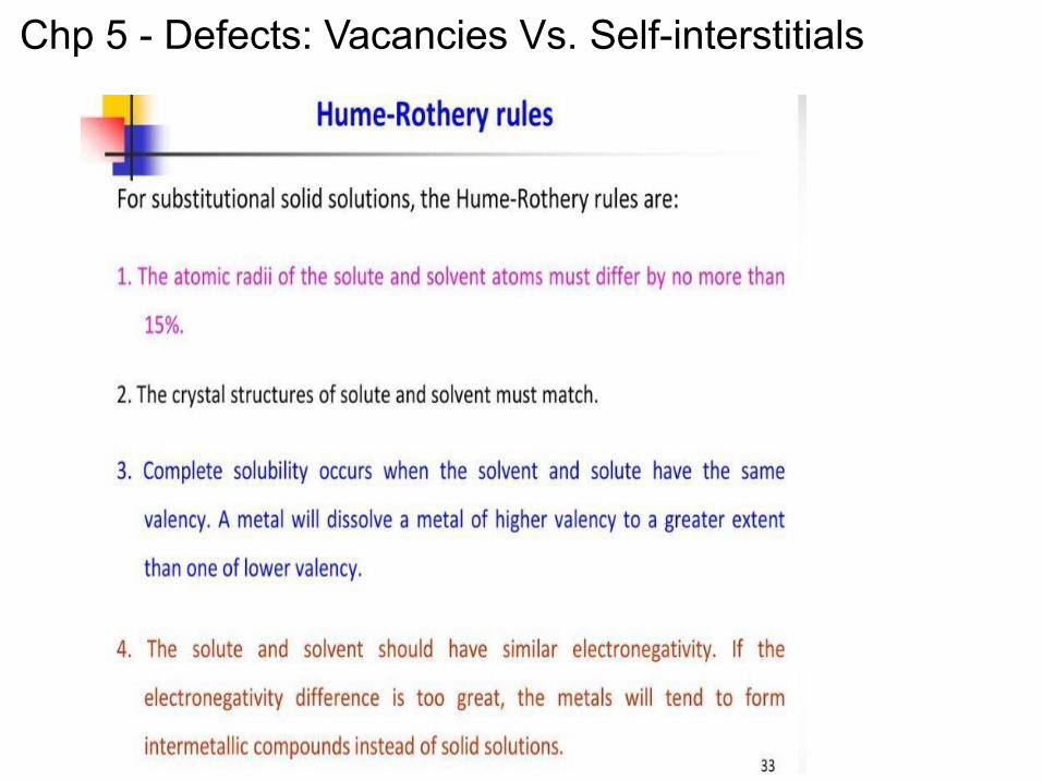
Chp 5 - Defects: Vacancies Vs. Self-interstitials

Chp 5 - Schottky and Frenkel Defects

0D Defects - Point Defects
Point Defects● Vacancies vs. self-interstitials● Solid solutions
● Substitutional● Substitutional solute or impurity atoms replace/ substitute host
atoms● Hume-Rothery rules for solubility (Atomic size factor, crystal
structure, electronegativity, valences)● Interstitial
● Impurity atoms fill voids or interstices among host atoms

1D Defects - Line Defects
Line Defects● Edge dislocation
● Linear defect, centered around line defined along end of extra half-plane of atoms (dislocation line)
● Screw dislocation● Helical path is traced around the linear defect (dislocation line) by the atomic planes
in the crystal lattice● Mixed dislocation
● Exhibits components of both screw and edge dislocations● Burgers vector
● Magnitude of direction of lattice distortion associated with dislocation● Edge dislocation: dislocation line perpendicular to Burgers vector● Screw dislocation: dislocation line parallel to Burgers vector

Chapter 6 - 16
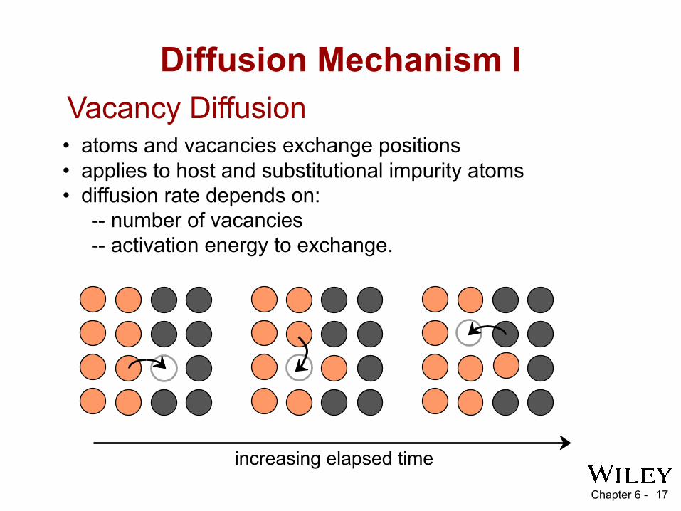
DiffusionDiffusion - Mass transport by atomic motion
• Interdiffusion - diffusion of atoms of one material into another material
• Self-diffusion – atomic migration in a pure metal
• Diffusion Mechanisms- Gases & Liquids – random (Brownian) motion- Solids – vacancy diffusion and interstitial
diffusion
Chapter 6 - 17
Diffusion Mechanism I
• atoms and vacancies exchange positions • applies to host and substitutional impurity atoms • diffusion rate depends on: -- number of vacancies -- activation energy to exchange.
increasing elapsed time
Vacancy Diffusion

Chapter 6 - 18
Diffusion Mechanism II
• Small, interstitial atoms move from one interstitial position to an adjacent one
More rapid than vacancy diffusionFig. 6.3 (b), Callister & Rethwisch 5e.
Interstitial Diffusion

Chapter 6 - 19
Rate of Diffusion• Diffusion is a time-dependent process.• Rate of Diffusion - expressed as diffusion flux, J
M =mass
diffusedtime
• Measured experimentally– Use thin sheet (or membrane) – cross-sectional area A– Impose concentration gradient across sheet– Measure mass of diffusing species (M) that passes through
the sheet over time period (t)

Chapter 6 - 20
Steady-State Diffusion
Fick’s first law of diffusionC1
C2
x
C1
C2
x1 x2
D = diffusion coefficient
Rate of diffusion (or flux) independent of timeFlux (J) proportional to concentration gradient:
C = concentrationx = diffusion direction
C

Chapter 7 - 21
• Simple tension:
Δl = Fl oEAo
Δd = - ν FdoEAo
• Deflection is dependent on material, geometric, and loading parameters.• Materials with large elastic moduli deform less
Useful Linear Elastic Relationships
Ao
Adapted from Fig. 7.9, Callister & Rethwisch 5e.

Chapter 7 - 22
Linear Elastic Properties
• Hooke's Law:σ = E ε
σ
Linear- elastic
• Modulus of Elasticity, E: (also known as Young's modulus)
E
ε
• Elastic deformation is nonpermanent and reversible! – generally valid at small deformations – linear stress strain curve
compression
tension
Units:E: [GPa] or [psi]1 GPa = 109 Pa

Chapter 7 - 23
Plastic Deformation
• Stress-strain plot for simple tension test:
stress, σ
strain, ε
Stressed into Plastic Region,Elastic + Plastic
εp
plastic strain
ElasticDeformation
Adapted from Fig. 7.10(a),Callister & Rethwisch 5e.
Stress Removed, Plastic Deformation Remains
• Plastic Deformation is permanent and nonrecoverable

Chapter 7 - 24
• Yield strength = stress at which noticeable plastic deformation has occurred
when εp = 0.002
Yield Strength
σy = yield strength
Note: for 5 cm sample
ε = 0.002 = Δz/z
Δz = 0.01 cm
Adapted from Fig. 6.10 (a),Callister & Rethwisch 9e.
σ (stress)
ε (strain)
σy
εp = 0.002
• Transition from elastic to plastic deformation is gradual

Chapter 7 - 25
Tensile Strength
• Metals: Maximum on stress-strain curve appears at the onset of noticeable necking
Adapted from Fig. 7.11, Callister & Rethwisch 5e.
σy
strain
Typical response of a metal
Fracture strength
Neck – acts as stress concentrator
eng
inee
ring
TS s
tress
engineering strain
• Tensile strength (TS) = maximum stress on engineering stress-strain curve.

Chapter 7 - 26
• Ductility = amount of plastic deformation at failure:• Specification of ductility -- Percent elongation:
-- Percent reduction in area:
Ductility
lfAo Af
lo
Adapted from Fig. 7.13, Callister & Rethwisch 5e.
tensile strain, ε
tensile stress, σ
low ductility
high ductility

Chapter 7 - 27
• Toughness of a material is expressed in several contexts • For this chapter, toughness = amount of energy absorbed before fracture • Approximate by area under the stress-strain curve—units of energy per unit volume
Toughness
Brittle fracture: small toughnessDuctile fracture: large toughness
very small toughness (unreinforced polymers)
tensile strain, ε
tensile stress, σ
small toughness (ceramics)
large toughness (metals)

Chapter 7 - 28
Mechanical PropertiesCeramic materials are more brittle than metals.
Why is this so?• Consider mechanism of deformation
– In crystalline, by dislocation motion– In highly ionic solids, dislocation motion is difficult
• few slip systems• resistance to motion of ions of like charge (e.g., anions) past
one another

Chapter 8 - 29
Motion of Edge and Screw Dislocations
• Direction of edge disl. line ( ) motion—in direction of applied shear stress τ.
Edge dislocation
Screw dislocation
Fig. 8.2, Callister & Rethwisch 5e.
• Direction of screw disl. line ( ) motion—perpendicular to direction of applied shear stress.

Chapter 8 - 30
Slip System—Combination of slip plane and slip direction – Slip Plane
• Crystallographic plane on which slip occurs most easily
• Plane with high planar density
– Slip Direction • Crystallographic direction along which slip occurs
most easily• Direction with high linear density
Slip Systems

Chapter 8 -
• For FCC crystal structure – slip system is– Dislocation motion on planes– Dislocation motion in directions– A total of 12 independent slip systems for FCC
31
Slip Systems (cont.)
Fig. 8.6, Callister & Rethwisch 5e.
direction
plane
• For BCC and HCP— other slip systems

Chapter 9 -
wt% Ni20 40 60 80 100
0
1000
1100
1200
1300
1400
1500
1600
T(°C)
L (liquid)
α
(FCC solidsolution)
L + αliquidussolidus
Cu-Niphasediagra
m
32
Phase Diagrams:Determination of phase(s) present
• Rule 1: If we know T and Co, then we know: -- which phase(s) is (are) present.
• Examples:A(1100°C, 60 wt% Ni): 1 phase: α
B
(1250°C, 35 wt% Ni): 2 phases: L + α
B
(125
0ºC
,35)
A(1100ºC,60)
Fig. 10.3(a), Callister & Rethwisch 5e. (Adapted from Phase Diagrams of BinaryNickel Alloys, P. Nash, Editor, 1991. Reprintedby permission of ASM International, MaterialsPark, OH.)

Chapter 9 - 33
• Rule 3: If we know T and C0, then can determine: -- the weight fraction of each phase.• Examples:
At TA: Only Liquid (L) present
WL = 1.00, Wα = 0
At TD:
Only Solid (α ) present
WL = 0, W
α = 1.00
Phase Diagrams:Determination of phase weight fractions
wt% Ni20
1200
1300
T(°C)
L (liquid)
α(solid)L + α
liquidus
solidus
30 40 50
L + α
Cu-Ni system
TAA
35C0
32CL
BTB
DTD
tie line
4Cα
3
R S
At TB:
Both α
and L present
= 0.27
WL= S
R +S
Wα= R
R +S
Consider C0 = 35 wt% Ni
Fig. 10.3(b), Callister & Rethwisch 5e. (Adapted from Phase Diagrams of BinaryNickel Alloys, P. Nash, Editor, 1991. Reprintedby permission of ASM International, MaterialsPark, OH.)

Chapter 9 - 34
• Tie line – connects the phases in equilibrium with each other – also sometimes called an isotherm
The Lever Rule
What fraction of each phase? Think of the tie line as a lever (teeter-totter)
ML Mα
R S
wt% Ni20
1200
1300
T(°C)
L (liquid)
α(solid)L + α
liquidus
solidus
30 40 50
L + αB
TB
tie line
C0CL Cα
SR
Adapted from Fig. 10.3(b), Callister & Rethwisch 5e.
Chapter 9 - 35
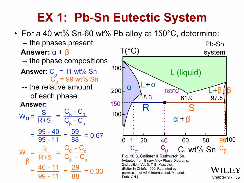
L+αL+β
α + β
200
T(°C)
18.3
C, wt% Sn20 60 80 1000
300
100
L (liquid)
α 183°C
61.9 97.8β
• For a 40 wt% Sn-60 wt% Pb alloy at 150°C, determine: -- the phases present Pb-Sn
system
EX 1: Pb-Sn Eutectic System
Answer: α + β-- the phase compositions
-- the relative amount of each phase
150
40C0
11Cα
99Cβ
SR
Answer: Cα = 11 wt% SnCβ = 99 wt% Sn
Wα =Cβ - C0Cβ - Cα
= 99 - 4099 - 11 = 59
88 = 0.67
SR+S =
Wβ
=C0 - CαCβ - Cα
=RR+S
= 2988
= 0.33= 40 - 1199 - 11
Answer:
Fig. 10.8, Callister & Rethwisch 5e. [Adapted from Binary Alloy Phase Diagrams, 2nd edition, Vol. 3, T. B. Massalski (Editor-in-Chief), 1990. Reprinted by permission of ASM International, Materials Park, OH.]

Chapter 9 - 36
• For alloys for which 2 wt% Sn < C0 < 18.3 wt% Sn• Result: at temperatures in α + β range -- polycrystalline with α grains and small β-phase particles
Fig. 10.12, Callister & Rethwisch 5e.
Microstructural Developments in Eutectic Systems II
Pb-Snsystem
L + α
200
T(°C)
C, wt% Sn10
18.3
200C0
300
100
L
α
30
α + β
400
(sol. limit at TE)
TE
2(sol. limit at Troom)
Lα
L: C0 wt% Sn
αβ
α: C0 wt% Sn

Chapter 9 - 37
• For alloy of composition C0 = CE • Result: Eutectic microstructure (lamellar structure) -- alternating layers (lamellae) of α and β phases.
Fig. 10.13, Callister & Rethwisch 5e.
Microstructural Developments in Eutectic Systems III
Fig. 10.14, Callister & Rethwisch 5e. (From Metals Handbook, 9th edition, Vol. 9,Metallography and Microstructures, 1985.Reproduced by permission of ASM International, Materials Park, OH.)
160 μm
Micrograph of Pb-Sn eutectic microstructure
Pb-Snsystem
L + β
α + β
200
T(°C)
C, wt% Sn20 60 80 1000
300
100
L
α
βL+ α
183°C
40
TE
18.3
α: 18.3 wt%Sn
97.8
β: 97.8 wt% Sn
CE61.9
L: C0 wt% Sn

Chapter 9 - 38
L+αL+β
α + β
200
C, wt% Sn20 60 80 1000
300
100
L
α
βTE
40
(Pb-Sn System)
Hypoeutectic & Hypereutectic
Fig. 10.8, Callister & Rethwisch 5e. [Adapted from Binary Alloy Phase Diagrams, 2nd edition, Vol. 3, T. B. Massalski (Editor-in-Chief), 1990. Reprinted by permission of ASM International, Materials Park, OH.]
160 μmeutectic micro-constituent
Fig. 10.14, Callister & Rethwisch 5e.
hypereutectic: (illustration only)
β
βββ
β
β
Adapted from Fig. 10.17, Callister & Rethwisch 5e. (Illustration only)
(Figs. 9.14 and 9.17 from Metals Handbook, 9th ed., Vol. 9, Metallography and Microstructures, 1985.Reproduced by permission of ASM International,Materials Park, OH.)
175 μm
α
α
α
ααα
hypoeutectic: C0 = 50 wt% Sn
Fig. 10.17, Callister & Rethwisch 5e.
T(°C)
61.9eutectic
eutectic: C0 = 61.9 wt% Sn

Chapter 9 - 39
• Eutectoid – one solid phase transforms to two other solid phasesS2 S1+S3 γ α + Fe3C (For Fe-C, 727°C, 0.76 wt% C)
intermetallic compound - cementite
coolheat
Eutectic, Eutectoid, & Peritectic• Eutectic - liquid transforms to two solid phases
L α + β (For Pb-Sn, 183°C, 61.9 wt% Sn) coolheat
coolheat
• Peritectic - liquid and one solid phase transform to a second solid phase S1 + L S2
δ + L γ (For Fe-C, 1493°C, 0.16 wt% C)

Chapter 9 - 40
Eutectoid & PeritecticCu-Zn Phase diagram
Fig. 10.21, Callister & Rethwisch 5e. [Adapted from Binary Alloy Phase Diagrams, 2nd edition, Vol. 2, T. B. Massalski (Editor-in-Chief), 1990. Reprinted by permission of ASM International, Materials Park, OH.]
Eutectoid transformation δ γ + ε
Peritectic transformation γ + L δ

Chapter 9 - 41
Iron-Carbon (Fe-C) Phase Diagram• 2 important points
- Eutectoid (B):
γ
⇒
α+
Fe3C
- Eutectic (A):
L
⇒
γ+
Fe3C
Fig. 10.28, Callister & Rethwisch 5e. [Adapted from Binary Alloy Phase Diagrams, 2nd edition, Vol. 1, T. B. Massalski (Editor-in-Chief), 1990. Reprinted by permission of ASM International, Materials Park, OH.]
Fe3C
(c
emen
tite)
160014001200100080060040001234566.7Lγ
(austenite)
γ
+L
γ
+Fe3C
α
+Fe3C
α+γδ(Fe)
C, wt% C
1148°C
T(°C)
α
727°C = Teutectoid
4.30Result: Pearlite = alternating
layers of α and Fe3C phases
120 μm
Fig. 10.31, Callister & Rethwisch 5e. (From Metals Handbook, Vol. 9, 9th ed.,Metallography and Microstructures, 1985.Reproduced by permission of ASM International, Materials Park, OH.)
0.76
B
γγγγ
A L+Fe3C
Fe3C (cementite-hard)
α
(ferrite-soft)

Chapter 9 - 42Fe
3C (c
emen
tite)
1600
1400
1200
1000
800
600
4000 1 2 3 4 5 6 6.7
L
γ (austenite)
γ+L
γ + Fe3C
α + Fe3C
L+Fe3C
δ
(Fe) C, wt% C
1148°C
T(°C)
α727°C
(Fe-C System)
C0
0.76
Hypoeutectoid Steel
Adapted from Figs. 10.28 and 10.33, Callister & Rethwisch 5e. [Adapted from Binary Alloy Phase Diagrams, 2nd edition, Vol. 1, T. B. Massalski (Editor-in-Chief), 1990. Reprinted by permission of ASM International, Materials Park, OH.]
Adapted from Fig. 10.34, Callister & Rethwisch 5e. (Photomicrograph courtesy of Republic Steel Corporation.)
proeutectoid ferritepearlite
100 μm Hypoeutectoidsteel
α
pearlite
γγ γ
γααα
γγγ γ
γ γγγ

Chapter 9 -Fe
3C (c
emen
tite)
1600
1400
1200
1000
800
600
4000 1 2 3 4 5 6 6.7
L
γ (austenite)
γ+L
γ + Fe3C
α + Fe3C
L+Fe3C
δ
(Fe) C, wt% C
1148°C
T(°C)
α727°C
(Fe-C System)
C0
43
Hypereutectoid Steel
0.76
C0
Fe3C
γγγ γ
γγγ γ
γγγ γ
Adapted from Fig. 10.37, Callister & Rethwisch 5e. (Copyright 1971 by United States Steel Corporation.)
proeutectoid Fe3C
60 μmHypereutectoid steel
pearlite
pearlite
Adapted from Figs. 10.28 and 10.36, Callister & Rethwisch 5e. [Adapted from Binary Alloy Phase Diagrams, 2nd edition, Vol. 1, T. B. Massalski (Editor-in-Chief), 1990. Reprinted by permission of ASM International, Materials Park, OH.]

Chapter 9 - 44
Electrical Properties• Which will have the greater resistance?
• Analogous to flow of water in a pipe• Resistance depends on sample geometry and
size.
D
2D
2

Chapter 9 - 45
Electrical Properties• Which will have the greater resistance?
• Analogous to flow of water in a pipe• Resistance depends on sample geometry and
size.
D
2D
2

Chapter 9 - 46
Extrinsic Semiconductors: Conductivity vs. Temperature
• Data for Doped Silicon: -- σ increases doping -- reason: imperfection sites lower the activation energy to produce mobile electrons.
• Comparison: intrinsic vs extrinsic conduction... -- extrinsic doping level: 1021/m3 of a n-type donor impurity (such as P). -- for T < 100 K: "freeze-out“, thermal energy insufficient to excite electrons. -- for 150 K < T < 450 K: "extrinsic" -- for T >> 450 K: "intrinsic"
Adapted from Fig. 12.17, Callister & Rethwisch 5e. (From S. M. Sze, Semiconductor Devices, Physics and Technology. Copyright © 1985 by Bell Telephone Laboratories, Inc. Reprinted by permission of John Wiley & Sons, Inc.)
Conduction electron concentration (1021/m3)T(K)
600400200
00123freeze-outextrinsicintrinsicdopedundoped

Chapter 9 - 47
DefinitionsFurther definitions
J = σ % <= another way to state Ohm’s law
J ≡ current density
% ≡ electric field potential = V/
Electron flux conductivity voltage gradient
J = σ (V/ )

Chapter 9 - 48
What is the minimum diameter (D) of the wire so that V < 1.5 V?
Example: Conductivity Problem
Cu wire I = 2.5 A- +
V
Solve to get D > 1.87 mm
< 1.5 V
2.5 A
6.07 x 10⁷ (Ohm-m)-1
100 m

Chapter 9 - 49
Conduction & Electron Transport• Metals (Conductors):-- for metals empty energy states are adjacent to filled states.
-- two types of band structures for metals
-- thermal energy excites electrons into empty higher energy states.
- partially filled band - empty band that overlaps filled band
filled band
Energy
partly filled band
empty band GA
P
fille
d st
ates
Partially filled band
Energy
filled band
filled band
empty band
fille
d st
ates
Overlapping bands

Chapter 9 - 50
Energy Band Structures: Insulators & Semiconductors
• Insulators: -- wide band gap (> 2 eV) -- few electrons excited across band gap
Energy
filled band
filled valence band
fille
d st
ates
GAP
emptyband
conduction
• Semiconductors: -- narrow band gap (< 2 eV) -- more electrons excited across band gap
Energy
filled band
filled valence band
fille
d st
ates
GAP
?
emptyband
conduction

Chapter 9 - 51
Charge Carriers in Insulators and Semiconductors
Two types of electronic charge carriers:
Free Electron – negative charge – in conduction band
Hole – positive charge
– vacant electron state in the valence band
Fig. 12.6 (b), Callister & Rethwisch 5e.
Move at different speeds - drift velocities

Chapter 9 - 52
Intrinsic Semiconduction in Terms of Electron and Hole Migration
Adapted from Fig. 12.11, Callister & Rethwisch 5e.
electric field electric field electric field
• Electrical Conductivity given by:
# electrons/m3 electron mobility
# holes/m3
hole mobility
• Concept of electrons and holes:
+-
electron hole pair creation
+-
no applied
applied
valence electron Si atom
applied
electron hole pair migration

Chapter 9 - 53
Number of Charge CarriersIntrinsic Conductivity
For GaAs ni = 4.8 x 1024 m-3
For Si ni = 1.3 x 10¹⁶ m-3
• Ex: GaAs
• for intrinsic semiconductor n = p = ni∴ σ = ni|e|(μe + μh)

Chapter 9 - 54
• Intrinsic: -- case for pure Si -- # electrons = # holes (n = p)• Extrinsic: -- electrical behavior is determined by presence of impurities that introduce excess electrons or holes -- n ≠ p
Intrinsic vs Extrinsic Conduction3+
• p-type Extrinsic: (p >> n)
no applied electric field
Boron atom
4+4+4+4+4+4+4+4+4+4+4+
hole
• n-type Extrinsic: (n >> p)
no applied electric field
5+
4+4+4+4+4+4+4+4+4+4+4+
Phosphorus atom
valence electron
Si atom
conductionelectron
Adapted from Figs. 12.12(a) & 12.14(a), Callister & Rethwisch 5e.

Chapter 9 - 55
Extrinsic Semiconductors: Conductivity vs. Temperature
• Data for Doped Silicon: -- σ increases doping -- reason: imperfection sites lower the activation energy to produce mobile electrons.
• Comparison: intrinsic vs extrinsic conduction... -- extrinsic doping level: 1021/m3 of a n-type donor impurity (such as P). -- for T < 100 K: "freeze-out“, thermal energy insufficient to excite electrons. -- for 150 K < T < 450 K: "extrinsic" -- for T >> 450 K: "intrinsic"
Adapted from Fig. 12.17, Callister & Rethwisch 5e. (From S. M. Sze, Semiconductor Devices, Physics and Technology. Copyright © 1985 by Bell Telephone Laboratories, Inc. Reprinted by permission of John Wiley & Sons, Inc.)
Conduction electron concentration (1021/m3)T(K)
600400200
00123freeze-outextrinsicintrinsicdopedundoped