morphology and optical measurements of nanostructured...
TRANSCRIPT

World Journal of Nano Science and Engineering, 2012, 2, 6-12 http://dx.doi.org/10.4236/wjnse.2012.21002 Published Online March 2012 (http://www.SciRP.org/journal/wjnse)
Morphology and Optical Measurements of Nanostructured In2O3:SnO2 Nanoparticle
A. Ayeshamariam1*, M. Jayachandran2, C. Sanjeeviraja3, M. Tajun Meera Begam4 1Department of Physics, Khadir Mohideen College, Adirampattinam, India
2ECMS Division, CECRI, Karaikudi, India 3School of Physics, Alagappa University, Karaikudi, India
4Department of Chemistry, Avvaiyar Government College for Women, Karaikal, India Email: *[email protected]
Received May 18, 2011; revised June 17, 2011; accepted October 20, 2011
ABSTRACT
Ultra-fine and uniform ITO nanopowders can be prepared by very simple Combustion method. In this paper, effects of Indium oxide with Sn doping on crystallinity, band gap values by UV studies and morphological studies by SEM and TEM analysis of nanopowders are reported. Powder mixtures of In2O3:SnO2 of 90:10 compositions are prepared and calculated grain size from X-ray diffraction measurements. The free electron absorption is determined from spectral transmission and reflection measurements. Key words: In2O3:SnO2, XRD, UV, Combustion and SEM. Keywords: In2O3:SnO2; XRD; UV; Combustion; SEM
1. Introduction
In2O3:SnO2 (also called indium tin oxide or ITO) is a highly degenerate n-type wide gap semiconductor that is produced by doping Sn atoms in In2O3. Since ITO pow- ders have a high transmittance in the visible range and a high conductivity simultaneously, they are widely used in a variety of electronic and optoelectronic fields. In Com- bustion process In2O3:SnO2 powders show an interest- ing and technologically important combination of prop- erties: they have luminous transmittance, high infrared reflectance, good electrical conductivity, excellent sub- strate adherence, hardness, and chemical inertness. Com- posite powders have been patented for use as agrochemi- cals and herbicides. Parent et al. [1] used extended X-ray absorption fine structure (EXAFS) investigations and found that the In atomic environment was modified by the Sn doping. Even at low tin concentrations the first oxygen polyhedron and the metallic In-In co-ordination shells were disordered. This disorder increases with the amount of tin inserted. Tin doped indium oxide is exten- sively studied as a base material for its gas sensor appli- cations. It is oxygen deficient and therefore is an n type semiconductor with a wide band gap (3.53 eV) [2]. The effect of crystallite size on the optical properties has been widely studied [3]. Nanocrystalline powders have at-tracted considerable interest because of their high trans- mittance. Here, we have presented the optical properties
of 90:10 nanocrystalline ITO powders [4].
1.1. Physical Characterization
The visible transmission was recorded using Hitachi S3400N Spectrophotometer. The calcined powders were further characterized by particle size analysis (Autosizer IIC Malvern) and powder X-ray diffraction (XRD) (X- ray diffractometer (XRD) with monochromation CuKα target (1.5406 Å) at a scan rate of 2˚C/min). Unit cell pa- rameter was calculated from the observed “d”-spacing, which was accurately measured with the help of silicon as an internal standard. Particle size and morphology of the synthesized powders were further evaluated with the help of a transmission electron microscope TEM (JEOL JEM 200CX). Scanning electron microscope (SEM) and Energy dispersive X-ray analysis (EDAX) work on the calcined powders were performed under Scanning Elec- tron Microscope Cambridge 53400N and elemental analy- sis was studied by EDAX Make “thermo software Nor- ton systems”. The asprepared powders were pelletised at a pressure of 500 kg/m2.
1.2. Experimental
The Combustion method is a useful technique that has been shown to be good preparation route for ITO nanopowders [5]. It is based on exothermic and usually very rapid chemical reaction between metal nitrates as an oxidizer and an organic fuel [6], such as Urea, glycine and so on. *Corresponding author.
Copyright © 2012 SciRes. WJNSE
A. AYESHAMARIAM ET AL. 7
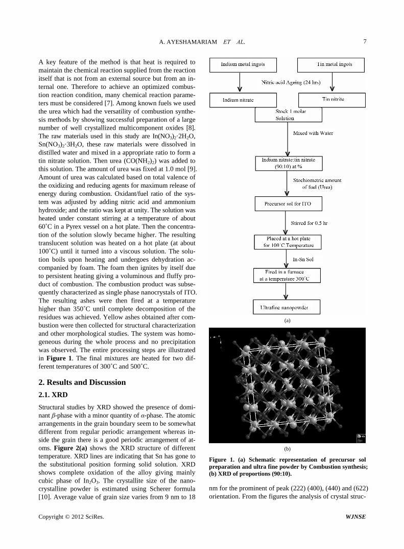
A key feature of the method is that heat is required to maintain the chemical reaction supplied from the reaction itself that is not from an external source but from an in- ternal one. Therefore to achieve an optimized combus- tion reaction condition, many chemical reaction parame- ters must be considered [7]. Among known fuels we used the urea which had the versatility of combustion synthe- sis methods by showing successful preparation of a large number of well crystallized multicomponent oxides [8]. The raw materials used in this study are In(NO3)2·2H2O, Sn(NO3)2·3H2O, these raw materials were dissolved in distilled water and mixed in a appropriate ratio to form a tin nitrate solution. Then urea (CO(NH2)2) was added to this solution. The amount of urea was fixed at 1.0 mol [9]. Amount of urea was calculated based on total valence of the oxidizing and reducing agents for maximum release of energy during combustion. Oxidant/fuel ratio of the sys- tem was adjusted by adding nitric acid and ammonium hydroxide; and the ratio was kept at unity. The solution was heated under constant stirring at a temperature of about 60˚C in a Pyrex vessel on a hot plate. Then the concentra- tion of the solution slowly became higher. The resulting translucent solution was heated on a hot plate (at about 100˚C) until it turned into a viscous solution. The solu- tion boils upon heating and undergoes dehydration ac- companied by foam. The foam then ignites by itself due to persistent heating giving a voluminous and fluffy pro- duct of combustion. The combustion product was subse-quently characterized as single phase nanocrystals of ITO. The resulting ashes were then fired at a temperature higher than 350˚C until complete decomposition of the residues was achieved. Yellow ashes obtained after com- bustion were then collected for structural characterization and other morphological studies. The system was homo-geneous during the whole process and no precipitation was observed. The entire processing steps are illustrated in Figure 1. The final mixtures are heated for two dif-ferent temperatures of 300˚C and 500˚C.
2. Results and Discussion
2.1. XRD
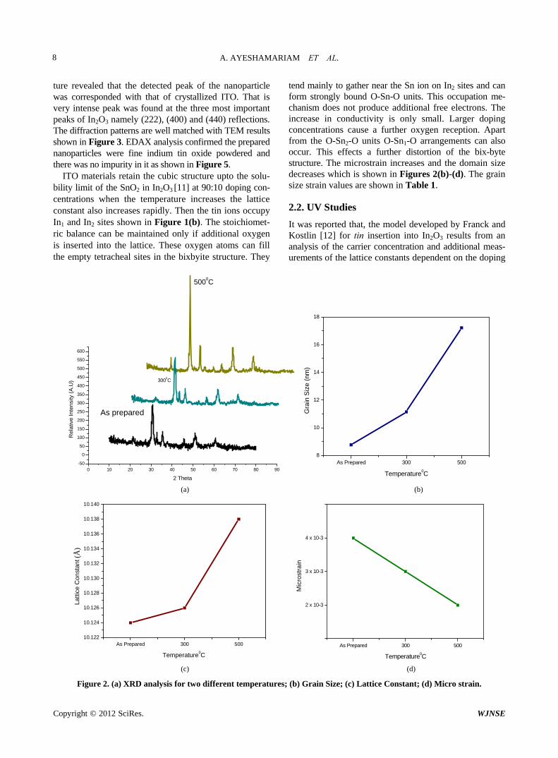
Structural studies by XRD showed the presence of domi- nant β-phase with a minor quantity of α-phase. The atomic arrangements in the grain boundary seem to be somewhat different from regular periodic arrangement whereas in-side the grain there is a good periodic arrangement of at- oms. Figure 2(a) shows the XRD structure of different temperature. XRD lines are indicating that Sn has gone to the substitutional position forming solid solution. XRD shows complete oxidation of the alloy giving mainly cubic phase of In2O3. The crystallite size of the nano- crystalline powder is estimated using Scherer formula [10]. Average value of grain size varies from 9 nm to 18
(a)
(b)
Figure 1. (a) Schematic representation of precursor sol preparation and ultra fine powder by Combustion synthesis; (b) XRD of proportions (90:10). nm for the prominent of peak (222) (400), (440) and (622) orientation. From the figures the analysis of crystal struc-
Copyright © 2012 SciRes. WJNSE
A. AYESHAMARIAM ET AL.
Copyright © 2012 SciRes. WJNSE
8
he solu- bi
tend mainly to gather near the Sn ion on In2 sites and can form strongly bound O-Sn-O units. This occupation me- chanism does not produce additional free electrons. The increase in conductivity is only small. Larger doping concentrations cause a further oxygen reception. Apart from the O-Sn2-O units O-Sn1-O arrangements can also occur. This effects a further distortion of the bix-byte structure. The microstrain increases and the domain size decreases which is shown in Figures 2(b)-(d). The grain size strain values are shown in Table 1.
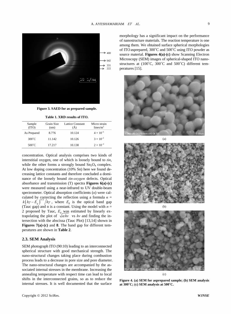
ture revealed that the detected peak of the nanoparticle was corresponded with that of crystallized ITO. That is very intense peak was found at the three most important peaks of In2O3 namely (222), (400) and (440) reflections. The diffraction patterns are well matched with TEM results shown in Figure 3. EDAX analysis confirmed the prepared nanoparticles were fine indium tin oxide powdered and there was no impurity in it as shown in Figure 5.
ITO materials retain the cubic structure upto tlity limit of the SnO2 in In2O3 [11] at 90:10 doping con-
centrations when the temperature increases the lattice constant also increases rapidly. Then the tin ions occupy In1 and In2 sites shown in Figure 1(b). The stoichiomet- ric balance can be maintained only if additional oxygen is inserted into the lattice. These oxygen atoms can fill the empty tetracheal sites in the bixbyite structure. They
2.2. UV Studies
It was reported that, the model developed by Franck and Kostlin [12] for tin insertion into In2O3 results from an analysis of the carrier concentration and additional meas- urements of the lattice constants dependent on the doping
0 10 20 30 40 50 60 70 80 90-50
0
50
100
150
200
250
300
350
400
450
500
550
600
Re
lativ
e In
ten
sity
(A
.U)
2 Theta
As prepared
3000C
5000C
As Prepared 300 5008
10
12
14
16
18
Gra
in S
ize
(n
m)
Temperature0C
(a) (b)
As Prepared 300 500
10.122
10.124
10.126
10.128
10.130
10.132
10.134
10.136
10.138
10.140
Latti
ce C
onst
ant (
A0)
Temperature0C
(Å)
As Prepared 300 500
2 x 10⁻³
3 x 10⁻³
4 x 10⁻³
Mic
rost
rain
Temperature0C (c) (d)
Figure 2. (a) XRD analysis fo (d) Micro strain.
r two different temperatures; (b) Grain Size; (c) Lattice Constant;
A. AYESHAMARIAM ET AL. 9
400
642
331222
Figure 3. SAED for as prepared sample.
Sample
Micro strain 2
Table 1. XRD results of ITO.
(ITO) Grain Size Lattice Constant
(nm) (Å) lines/m
As Prepared 8.776 10.124 4 × 10⁻³
300˚C 11.142 10.126 3 × 10⁻³
500˚C 17.217 10.138 2 × 10⁻³
oncentration. Optical analysis comprises two kinds of c
interstitial oxygen, one of which is loosely bound to tin, while the other forms a strongly bound Sn2O4 complex. At low doping concentration (10% Sn) here we found de- creasing lattice constants and therefore concluded a domi- nance of the loosely bound tin-oxygen defects. Optical absorbance and transmission (T) spectra Figures 6(a)-(c) were measured using a near-infrared to UV double-beam spectrometer. Optical absorption coefficients (α) were cal- culated by correcting the reflection using a formula α = /2n
gk h E h , where Eg is the optical band gap (Tauc n s a constant. Using the model with n = 2 proposed by Tauc, Eg was estimated by linearly ex-trapolating the plot of
gap) and i
hv vs hv and finding the in-tersection with the abscissa auc Plot) [13,14] shown in Figures 7(a)-(c) and 8. The band gap for different tem-peratures are shown in Table 2.
2.3. SEM Analysis
(T
90:10) leading to an interconnected
ance
SEM photograph ITO (spherical structure with good mechanical strength. The nano-structural changes taking place during combustion process leads to a decrease in pore size and pore diameter. The nano-structural changes are accompanied by the as- sociated internal stresses in the membrane. Increasing the annealing temperature with respect time can lead to local shifts in the interconnected grains, so as to reduce the internal stresses. It is well documented that the surface
of nanostructure materials. The reaction temperature is one among them. We obtained surface spherical morphologies of ITO asprepared, 300˚C and 500˚C using ITO powder as source material. Figures 4(a)-(c) show Scanning Electron Microscopy (SEM) images of spherical-shaped ITO nano- structures at (100˚C, 300˚C and 500˚C) different tem- peratures [15].
morphology has a significant impact on the perform
(a)
(b)
(c)
Figure 4. (a) SEM for asprepared sample; (b) SEM analysis at 300˚C; (c) SEM analysis at 500˚C.
Copyright © 2012 SciRes. WJNSE

A. AYESHAMARIAM ET AL. 10
Figure 5. EDAX.
0 500 1000 1500 2000 25000
20
40
60
80
100
Asp 90% 10%
% o
f Tra
nsm
issi
on
Wavelength (nm) (a)
0 500 1000 1500 2000 25000
20
40
60
80
100
300 ITO 90% 10%
% o
f Tra
nsm
issi
on
Wavelength (nm)
0 500 1000 1500 2000 25000
20
40
60
80
100
500 ITO 90% 10%
% o
f Tra
nsm
issi
on
Wavelength (nm) (c)
Figure 6. Transmittance cu of (a) ASP; (b) 300˚C; (c500˚C.
rves )
(a)
(b) (b)
Copyright © 2012 SciRes. WJNSE
A. AYESHAMARIAM ET AL. 11
(c)
Figure 7. Band gap values of (a) ASP; (b) 300˚C; (c) 500˚C.
Figure 8. Grain size and bandgap values of ITO.
Table 2. Bandgap values of ITO.
Sample (ITO) Bandgap (eV)
As prepared 3.197
300˚C 3.156
500˚C 3.135
2.4. Sensor Analysis
The addition of a small amount of doping elements to SnO2 powders has been known to be effective in modi-fying their optical and electrical properties [16]. In par-ticular, in the case of gas sensor applications, a gene strategy for tailoring mate e selective sensor
ddition of dopants during sensor fabrication [17]. Hence, there is a growing interest in doping SnO2 with different
ralrials for th
response involves the modification of the surface by the a
0 150 300 450 600 750 900
In2O
3 90% SnO
2 10%
Se
nsi
tivity
Time (Sec)
0815
0.79
0.77
0.75
0.73
0.71
0.69
0.65
igure 9. Sensitivity with respect to time of as prepared sam- ple. element ent study, we o ease in grain siz rease in temperatur of the samp epared is of the order nm. In this works, grai effects on the sensitiv gas sensor devices have reported shown in Figure 9.
But the powders are highly resistive. Hence, In2O3:SnO2 dopings can be used in areas where only a moderate elec- tronic conductivity is required.
REFERENCES [1] G. Franck and H. Kostlin, “Electrical Properties and De-
fect Model of Tin-Doped Indium Oxide Layers,” Applied Physics A: Materials Science & Processing, Vol. 27, No. 4, 1982, pp. 197-206. doi:10.1007/BF00619080
F
s. In the pres bserved incre due to inc e. The grain size
les pr of 9 n size
been ity of
3. Conclusion
The experimental studies revealed that the sensitivity is enhanced when the grain size is decreased. Also Xu et al. [18] have observed that, by reducing the particle size (~6 nm), high gas sensitivity and short response times can be achieved. In our research the study of indium-doped SnO2 powders, it has been concluded that uniform, homoge- nous and highly transparent powders with small grain size 9 nm can be prepared by indium doping on tin oxide.
[2] C. G. Fonstad and R. H. Rediker, “Electrical Properties of High-Quality Stannic Oxide Crystals,” Journal of Applied Physics, Vol. 42, No. 7, 1971, p. 2911. doi:10.1063/1.1660648
[3] X. Wang, S. S. Yee and W. P. Carey, “Transition between Neck-Controlled and Grain-Boundary-Controlled Sensi- tivity of Metal-Oxide Gas Sensors,” Sensors and Actua-tors B: Chemical, Vol. 25, No. 1-3, 1995, pp. 454-457. doi:10.1016/0925-4005(94)01395-0
[4] L. Abello, B. Bochu, A. Gaskov, S. Koudryavtseva, G.
Copyright © 2012 SciRes. WJNSE

A. AYESHAMARIAM ET AL.
Copyright © 2012 SciRes. WJNSE
12
Lucazeau and M. Roumyantseva, “Structural Characteri-zation of Nanocrystalline SnO2 by X-Ray and Raman Spectroscopy,” Journal of Solid State Chemistry, Vol. 135, No. 1, 1998, pp. 78-85. doi:10.1006/jssc.1997.7596
[5] J. H. Kang, J. Y. Kim and D. Y. Jeona, “Synthesis and Characterization of Orange Emitting SnO2: Eu3+ Phos-phor by an Optimized Combustion Method,” Journal of
mical Society, Vol. 152, No. 3, pp. H33-the ElectrocheH38.
[6] L. E. Shea, J. Mukittrick and O. A. Lopez “Synthesis of Red-Emitting, Small Particle Size Luminescent Oxides Using an Optimized Combustion Process,” Journal of the American Ceramic Society, Vol. 79, No. 12, 1996, pp. 3257-3265. doi:10.1111/j.1151-2916.1996.tb08103.x
[7] S. R. Jain, K. C. Adiga and V. R. P. Verneker, “A New Approach to Thermochemical Calculations of Condensed Fuel-Oxidizer Mixtures,” Combustion and Flame, Vol. 40, 1981, pp. 71-79. doi:10.1016/0010-2180(81)90111-5
[8] A. S. Mukasyan, C. Costllo, K. P. Sherlock, D. Lafarga and A. Varma, “Perovskite Membranes by Aqueous Com- bustion Synthesis: Synthesis and Purification Technology
and Properties,” Separation , Vol. 25, No. 1-3, 2001, pp
117-126. doi:.
10.1016/S1383-5866(01)00096-X
[9] J. H. Kang, J. , Proceeding of the
uum Sci-
Y. Kim and D. Y. Jean 3rd International Meeting on information display, Daegu, 2002.
[10] H. Wulff and C. Eggs, “Investigation of Stored Energy in Plasma Deposited TiNx Films,” Journal of Vacence & Technology A, Vol. 15, No. 6, 1997, p. 2938. doi:10.1116/1.580888
[11] A. R. Stokes, “A Numerical Fourier-Analythe Correction of Width
sis Method for s and Shapes of Lines on X-ray
Powder Photographs,” Proceedings of the Physical Soci-ety, Vol. 6, No. 4, 1948, p. 382. doi:10.1088/0959-5309/61/4/311
[12] Y. Ohhata, F. Shinoki and S. Yoshida, “Optical Properties of r.f. Reactive Sputtered Tin-Doped In2O3 Films,” Thin Solid Films, Vol. 59, No. 2, 1979, pp. 255-261. doi:10.1016/0040-6090(79)90298-0
[13] J. Tauc, R. Grigorovici and A. Vancu, “Optical Properties and Electronic Structure of Amorphous Germanium,” Physica Status Solidi (b), Vol. 15, No. 2, 1966, pp. 627- 637. doi:10.1002/pssb.19660150224
[14] J. Tauc, “Amorphous and Liquid Semiconductors,” In: J.
ed e Obtained by the Sol-Gel Method
Tauc, Ed., Plenum, New York, 1979.
[15] A. Gurlo, N. Barsan, U. Weimar, M. Ivanovskaya, A. Taurino and P. Siciliano, “Polycrystalline Well-ShapBlocks of Indium Oxidand Their Gas-Sensing Properties,” Chemistry of Mater- ials, Vol. 15, No. 23, 2003, pp. 4377-4383. doi:10.1021/cm031114n
[16] P. S. Devi, M. Chatterjee and DOxide Nano-Particles through an
. Ganguli, “Indium Tin Emulsion Technique,”
Material Letters, Vol. 55, No. 4, 2002, pp. 205-210. doi:10.1016/S0167-577X(01)00647-4
[17] S. Ramanan, “Dip coated ITO Thin-Films throuGel Process Using Metal Salts,” Th
gh Sol- in Solid Films, Vol.
389, No. 1-2, 2001, pp. 207-212. doi:10.1016/S0040-6090(01)00825-2
[18] H. Y. Xu, X. L. Liu, D. L. Cui, M. Li and M. H. Jiang, “A Novel Method for Improving the Performance of ZnO Gas Sensors,” Sensors and Actuators B: Chemical, Vol. 114, No. 1, 2006, pp. 301-307. doi:10.1016/j.snb.2005.05.020