more advanced test equipment construction
TRANSCRIPT

More Advanced Test Equipment Construction
1 / ///////////IIIIIIIII\IMV\\\\\\\Nz,,

MORE ADVANCED TEST EQUIPMENT CONSTRUCTION

Other Titles of Interest
BP70 Transistor Radio Fault Finding Chart BP101 How to Identify Unmarked IC's BP110 How to Get Your Electronic Projects Working BP120 Audio Amplifier Fault Finding Chart BP239 Getting the Most From Your Multimeter BP248 Test Equipment Construction BP265 More Advanced Uses of the Multimeter BP267 How to Use Oscilloscopes and Other Test Equipment

MORE ADVANCED TEST EQUIPMENT CONSTRUCTION
by
R. A. PENFOLD
BERNARD BABANI (publishing) LTD THE GRAMPIANS
SHEPHERDS BUSH ROAD LONDON W6 7NF
ENGLAND

Please Note
Although every care has been taken with the production of this book to ensure that any projects, designs, modifications and/or programs etc. contained herewith, operate in a correct and safe manner and also that any components specified are normally available in Great Britain, the Publishers do not accept respon-sibility in any way for the failure, including fault in design, of any project, design, modification or program to work correctly or to cause damage to any other equipment that it may be connected to or used in conjunction with, or in respect of any other damage or injury that may be so caused, nor do the Publishers accept responsibility in any way for the failure to obtain specified components.
Notice is also given that if equipment that is still under warranty is modified in any way or used or connected with home-built equipment then that warranty may be void.
ID 1989 BERNARD BABANI (publishing) LTD
First Published — November 1989
British Library Cataloguing in Publication Data
Penfold, R. A. More advanced test equipment construction
1. Electronic testing equipment. Construction
I. Title
621.3815'48
ISBN 0 85934 194 1
Preface
Anyone involved with electronic project construction soon realises the importance of having a reasonable range of test equipment. Newly constructed projects can and do fail to work from time to time, and operational projects can develop faults. Without test equipment it is possible to track down wiring errors, accidental short circuits, etc., but difficult faults such as "dud" components can be very difficult and time consuming to track down without the aid of some test gear.
The book "Test Equipment Construction" (BP248) des-cribes some simple but useful items of test equipment that are designed to fill in most of the gaps in the average multimeter's repertoire. This publication provides further designs for the electronics hobbyists' workshop. In some cases these are more sophisticated versions of equipment featured in the earlier book, but in most cases they are for equipment of a type not featured in it. A range of useful digital measuring instruments are described in Chapter 1, with a few miscellaneous designs being provided in Chapter 2. The projects include a current tracer, a high quality digital capacitance meter, a dynamic transistor tester, and a crystal calibrator.
Unlike "Test Equipment Construction" (BP248), this book is not primarily aimed at beginners and near beginners at electronic project construction. A certain amount of practical experience and knowledge of electronics theory is assumed. However, you do not need to be an expert at electronics in order to build and use these designs, and anyone with a moderate amount of electronics experience should be able to tackle these projects. Someone who has gained some experi-ence by building and using projects from BP248 should be able to successfully undertake and utilize the designs featured here.
R. A. Penfold

Warning
Never make tests on any mains powered equipment that is plugged into the mains unless you are quite sure you know exactly what you are doing.
Remember that capacitors can hold their charge for some considerable time even when equipment has been switched off and unplugged.

Contents
Page Chapter 1: DIGITAL MEASURING EQUIPMENT 1
Half Digits 1 Single Integration 2 D.V.M. Circuit 3 Interconnections 8 High Resistance Voltmeter 13 Attenuator Circuit 16 Audio Frequency Meter 18 Frequency to Voltage Converter Circuit 22 Calibration 25 Capacitance Meter 26 The Circuit 31 Calibration 33 Resistance Meter 37 The Circuit 39 Transistor Tester 42 The Circuit 44 Current Tracer 49 The Circuit 51 Heatsink Thermometer 53 Mains PSU 57
Chapter 2: MISCELLANEOUS TEST GEAR PROJECTS 61 Crystal Calibrator 61 The Circuit 63 Bench Power Supply 69 The Circuit 71 Construction 75 Setting Up 77 Logic Pulser 78 Circuit Operation 80 The Circuit 82 Dynamic Transistor Tester 85 The Circuit 89
Semiconductor Leadout and Pinout Details 94

GFAB GFABGFA X Z 3333 L22221 1 1
40 fl 71, 7 7 77 7 77777777 7177rin 21
1 LJLILILILILJLJULJULJULIULJULJULJ Li 2o
BYK DEDCDEDCDEDCB P333P 222 P 1 1 1 1 3 2 1
Fig. 1.5 Pin out details for the liquid crystal display
Note that the half digit of the display is a single segment ("AM" on the d.v.m. chip and "K" on the display). "BP" is the backplane terminal, and the minus segment ("Y" of the display) is driven from the "Pol" (polarity) output of the ICL7106. Incidentally, the ICL7106 will accept an input of either polarity, with the "—" segment being automatically activated if there is a reverse polarity input. This is very useful when the unit is used as a voltmeter, but may be inappropriate when it is used in certain types of test equip-ment. In the case of a transistor tester for example, the gain can never be a negative figure. Accordingly, the "Y" segment of the display should be left unconnected when the d.v.m. module is used in a unit of this type.
Most three and a half digit liquid crystal displays have other segments, such as "+" and "Bat" types, but these are left unused in this case. It should be pointed out that the pinout details of Figure 1.5 are correct for the display I used, and for the three and a half digit liquid crystal displays offered
10

Notes
100

Notes
101

Chapter 1
DIGITAL MEASURING EQUIPMENT
Test equipment falls into two main categories — those devices that measure something and those that generate signals of one kind or another. In this first chapter we will consider several pieces of measuring equipment. Something they all have in common is that they are digital instruments. In fact they are all based on the same three and a half digit d.v.m. (digital voltmeter) module. First the digital voltmeter module will be described, and then we will move on to a range of add-ons that will enable it to perform a range of useful functions.
Half Digits There are several digital voltmeter integrated circuits available, and these enable highly accurate voltmeters to be produced using a minimal number of components. It is not actually all that difficult to produce a d.v.m. from logic circuits and linear devices, but a special d.v.m. integrated circuit will generally provide better accuracy at lower cost, and with a much lower parts count. The less expensive d.v.m. chips are designed to drive three and a half digit displays. In other words, a four digit display where the most significant digit can only be zero or one. In fact it is more accurate to say that the most signifi-cant digit is either blanked out or is set at 1. It has only two segments, and can not display a leading zero (but presumably would never need to anyway).
The use of a so-called half digit might seem a bit gimmicky, but it is really quite a good arrangement. With digital test equipment it is normal to have each measuring range one decade higher than the previous one. A digital resistance meter for instance, might have ranges of 999 ohms, 9.99k, 99.9k, 999k, and 9.99M full scale. A slight problem with this arrangement is that some values produce an over-range error on cne range, but quite a low reading on the next range up. For instance, a resistor having a value of 1024 ohms would give an over-range indication on the 999 ohms range, and a far from full scale reading of 1.02k on the 9.99k range. This
1
tends to give limited accuracy on these awkward values, although it has to be said that for most purposes results would still be perfectly adequate. Anyway, the extra half digit enables these values to be brought in-range on the lower range, giving better accuracy.
Four and a half digit d.v.m. chips offer extremely good specifications, and give the potential for very high degrees of accuracy. They are relatively expensive though, and in prac-tical applications it is very difficult to produce an overall design that justifies the extra digit. With a three and a half digit display each increment of the least significant digit represents just 0.05% of the full scale value. The equivalent figure for a four and a half digit display is 0.005%! With the circuits preceding the d.v.m. being built using what will at best be 1% tolerance components, even a three and a half digit display could be regarded as being over-specified. There is no realistic prospect of producing circuits to exploit the_ full resolution and accuracy of a four and a half digit d.v.m. The circuits in this book are therefore based on an ordinary three and a half digit d.v.m. design.
Chips to drive light emitting diode (1.e.d.) and liquid crystal displays (1.c.d.) are available. As far as using the instruments is concerned, 1.e.d.s are better in dim lighting while 1.c.d.s are superior under bright conditions. There is little overall advan-tage to either type in this respect. I chose to base these cir-cuits on a chip which operates with a liquid crystal display simply because this type of display requires a much lower operating current. In fact the whole d.v.m. circuit draws a supply current of only about two milliamps or so. This permits economic battery operation, and even a small (PP3 size) 9 volt battery will have a long operating life. The current consump-tion for the 1.e.d. equivalent of this d.v.m. circuit would be largely dependent on the number of segments switched on at the time, and the particular 1.e.d. segment current used, but would probably exceed one hundred milliamps on occasions. This would necessitate the use of a high capacity battery which would still have a relatively limited operating life.
Single Integration Digital voltmeters almost invariably use the single or dual
2

slope integration techniques. The ICL7106 d.v.m. chip used in the designs described in this chapter is of the single slope integration variety. This is somewhat inferior to the dual slope type in certain respects, but it is nevertheless capable of providing excellent results. The single slope integration pro-cess operates by having a clock oscillator driving the input of a counter circuit via a gate circuit. In practical systems the counter drives the display via latches which have their contents up-dated each time a new value is available from the counter. This gives a continuous display of the input voltage, with the counting process not being apparent to the user.
In order to give a reading of the input voltage, some means of converting the input voltage to a gate pulse of proportional length is required. This is achieved using an integrator, which is a circuit that charges a capacitor at a rate that is proportion-al to the input voltage. There is more than one way of using an integrator in a d.v.m., one of which is to compare the output voltage of the integrator witti the input voltage. An input pulse to the integrator starts its output rising in voltage at a linear rate. When the output voltage of the integrator reaches the same potential as the input voltage, the input pulse is ended. The input pulse can be generated using a flip/flop which is set by the control logic circuit to start the input pulse, and reset by the comparator to end it.
The point to note here is that the higher the input voltage, the longer it will take the output voltage of the integrator to reach the input potential. As the integrator's output rises at a linear rate, the duration of the integrator's input pulse is proportional to the input voltage, and can therefore be used as the gate pulse. The block diagram of Figure 1.1 helps to explain the way in which the various stages interconnect, but this is in somewhat over-simplified form. In practice some fairly complex control logic circuits are needed in order to get everything functioning properly.
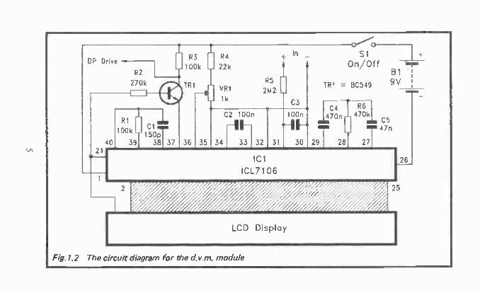
D.V.M. Circuit The full circuit diagram of the digital voltmeter module appears in Figure 1.2. R5 and C3 merely form a lowpass filter at the input of the circuit. It is standard practice to include a filter of this type at the input of d.v.m.s since any noise on
3

Input
Pulse
Generator
Integrator Voltage
Compar.
Flip/Flop
Clock
Oscillator
Gate
3.5 Digit Counter
Latches
3.5 Digit L.C.D. Display
Fig. 1.1 Simplified block diagram for a single slope integration d.v.m.
the input tends to cause variations in the displayed reading. This can make the display very difficult to read, and a lowpass filter with a low cut-off frequency greatly eases the problem by smoothing out the variations in the input voltage so that much more stable readings are obtained. A fairly low cut-off fre-quency is desirable as it gives a large amount of smoothing and very stable readings. On the other hand, this results in a significant delay between a new input voltage being applied to
4
DP Drive
21 o
R2
270k
I I
RI
R3 100k
TRI
Cl 100k
T 150p 39I 38 37 36 35
R4
22k
VR1
1k
R5
2112
34
C2 100n
33 I 32 31
Si On/Off
Bi
TR 1 = BC549 9V
100n 470n C4 I R6
470k
C3
11-6 C5 471
30 29 81 27
26
ICL7106
25
LCD Display
Fig. 1.2 The circuit diagram for the d.v.m. module

the circuit and the display adjusting to reflect this new input level. The specified values give excellent smoothing, but in some applications you might prefer to set the cutoff frequency of the filter somewhat higher by making C3 lower in value.
VR1 and R4 form part of a reference voltage generator. VR1 enables the sensitivity of the circuit to be adjusted for calibration purposes, and a fairly wide adjustment range is available. The nominal full scale input voltage is 200 milli-volts (or 199.9 millivolts if you wish to be pedantic). In this book there will often be references to (say) a 2 volt range when the actual full scale value is 1.999 volts. This is a method of abbreviation which is often to be found in the specifications sheets and operating manuals of digital instruments.
RI and Cl are discrete components in the clock generator circuit, and their precise values are not important. They do not affect the accuracy of the unit, but merely set the rate at, which readings are taken and the display is updated. With the suggested values the display is updated about twice a second, which is about the optimum for most digital measur-ing instruments.
R2, R3, and TRI generate a signal that can be used to drive a decimal point segment of the display. Liquid crystal displays are not driven with a d.c. signal, like the ones used for 1.e.d. displays. A d.c. signal will in fact activate a liquid crystal display, but segment "burn" will soon occur, render-ing the display useless. Apparently d.c. signals can cause damage very rapidly indeed — possibly within a matter of minutes. In order to obtain a long operating life the display must be driven with an a.c. signal, and one which has no significant d.c. bias. The normal way of driving liquid crystal displays with a suitable signal is to apply a squarewave signal to the backplane (BP) input (the equivalent of the "common" terminal on a 1.e.d. display), and an inverted version of that signal to any segment that must be switched on. Electronic switches turn the output signals on or off, as required. Here TR1 operates as a simple inverter stage which provides an anti-phase version of the backplane signal. It has its emitter connected to the "Test" terminal of IC1 rather than to the 0 volt supply rail, so that it provides an output signal having
6
the correct voltage range. Most of the other components are either part of the inte-
grator or the automatic zeroing circuit. Due to the inclusion of an effective automatic zeroing circuit, no manual zero adjustments at all are required (but there may be voltage offsets in the circuit driving the d.v.m. which will need to be manually nulled).
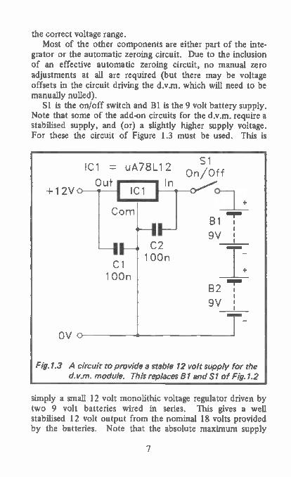
Si is the on/off switch and B1 is the 9 volt battery supply. Note that some of the add-on circuits for the d.v.m. require a stabilised supply, and (or) a slightly higher supply voltage. For these the circuit of Figure 1.3 must be used. This is
S1 ICi --= uA78L12
On/Off Out In
+12V
100n
OV
02 100n
Cl
0 +
T_ B2
9V
Fig. 1.3 A circuit to provide a stable 12 volt supply for the d.v.m. module. This replaces 81 and Si of Fig. 1.2
simply a small 12 volt monolithic voltage regulator driven by two 9 volt batteries wired in series. This gives a well stabilised 12 volt output from the nominal 18 volts provided by the batteries. Note that the absolute maximum supply
7
voltage rating of the ICL7106 d.v.m. chip is 15 volts, and it is not safe to use the 18 volt battery supply without the voltage regulator. It is a good idea to check that the correct 12 volt supply is being obtained from the finished circuit prior to fitting the d.v.m. chip into its socket.
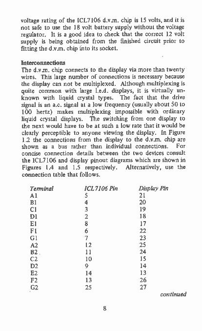
Interconnections The d.v.m. chip connects to the display via more than twenty wires. This large number of connections is necessary because the display can not be multiplexed. Although multiplexing is quite common with large 1.e.d. displays, it is virtually un-known with liquid crystal types. The fact that the drive signal is an a.c. signal at a low frequency (usually about 50 to 100 hertz) makes multiplexing impossible with ordinary liquid crystal displays. The switching from one display to the next would have to be at such a low rate that it would be clearly perceptible to anyone viewing the display. In Figure 1.2 the connections from the display to the d.v.m. chip are shown as a bus rather than individual connections. For concise connection details between the two devices consult the ICL7106 and display pinout diagrams which are shown in Figures 1.4 and 1.5 respectively. Alternatively, use the connection table that follows.
Terminal ¡CL 7106 Pin Display Pin Al 5 21 B1 4 20 Cl 3 19 D1 2 18 El 8 17 Fl 6 22 G1 7 23 A2 12 25 B2 11 24 C2 10 15 D2 9 14 E2 14 13 F2 13 26 G2 25 27
continued
8

1
V+ cr D1 a Cl B1 a Al a Fl a G1 a El a D2 a C2 a 82 CI A2 a F2 a E2 03 a 83 cl F3 a E3 ct
AB4 a Pol a
20
40
• Oscl • Osc2 D Osc3 D Test D Ref Hi D Ref Low • C+ Ref • C— Ref D Common D In Hi D In Low • A/Z D Buff D Int D V— D G2 D C3 D A3 D G3 D BP
21
Fig. 1.4 The ICL7106 pinout details
Terminal A3 B3 C3 D3 E3 F3 G3 AB4/K BP Pol/Y
¡CL 7106 Pin Display Pin 23 30 16 29 24 11 15 10 18 9 17 31 22 32 19 3 21 1 20 2
9

Please note following is a list of other titles that are available in our range of Radio, Electronics and Computer Books.
These should be available from all good Booksellers, Radio Component Dealers and Mail Order Companies.
However, should you experience difficulty in obtaining any title in your area, then please write directly to the publisher enclosing payment to cover the cost of the book plus adequate postage.
If you would like a complete catalogue of our entire range of Radio, Electronics and Computer Books then please send a Stamped Addressed Envelope to:
BERNARD BABANI (publishing) LTD THE GRAMPIANS
SHEPHERDS BUSH ROAD LONDON W6 7NF
ENGLAND
102

180 Coil Design and Coretruction PA•nual £2.50 205 H.P. Loudspeaker Enclosure. £2.95 208 Prectical Stereo &Ocedrophony H.ndbook £0 75 214 Audio Enthusiast'. Handbook £0.85 219 Solid State Novelty Projects £0.85 220 Budd Your Own Solid St.te Hi -Fi and Audio Accewortes £0.85 222 Solicl State Short Wave Receiver. for Beginners £2.95 225 A Prectical Introduction to Digital ICs £2.50 228 How to Budd Acheniad Short Wave Renwen £2.96 227 Bniinner. Guid• to Buiklere E bctronic Project. f 1 96 228 Encored Theory for the Electronics Hobbynet £2.50 SP? Handbook of Radio, TV, Industrial and Transmitting Tube and Val. Equiyelents £0.60 BP6 Engrneer'•& Mechinist's Reference Tables £1.25 BPI Radio 6 Electronic Colour Code. D.ta Chart £0.95 5077 Chart of Redio, Electronic, Semiconductor and Logo Symbols £0.95 BP28 Rotator Selection Handbook £0.60 BP29 NI•jor $olid State Audio H.P. Construction PrOjKli £0.85 B1'33 Electronic Calculator Wen Handbook f 1.50 BP36 50 Circuit. Using Germanium Silicon wId Zane Diode. £1.50 BP37 50 Project. Using Relays, SCRs and TR IAC. £2.96 BP39 50 IFETI Field Effect Trensistor Projects £2.96 BP42 50 Simple LED Circuit. £1.96 BP44 IC 555 Projects £2.95 BP45 Projects in Opto.Electronics £1.95 BP48 Electronic Projects for Beginners £1.96 BP49 Popular Electronic Project. £2.50 BPS? Procne.. Eictronics Calculetion. and Formulae £3.96 8P54 Your Ekoctronic Calculator & Your Morey £1.35 BP56 Electronic Security Devices £2.50 BP58 50 Circuits Using 7400 Sere. IC's £2.50 BP62 The Simple Electromc Circuit & Components lElernents of Electronics - Book 1/ £3.50 BP63 Alternating Currott Theory 'Elements of Electronics - Book 21 £3.50 BPS., Senn...doctor Technology lEbnients of Electronics - Book 31 £3.50 13E56 Beginners Guide to Microprocemon and Computing BP68 Choosing arid Using Your Hi-Fi £1.65 BP69 Electronic Garner £1.75 BP70 Tr.nsetor Radio Fault.f iodine Chet £0.95 BP72 A Microprocessor Pruner £1.75 BP74 Electronic Music Projects £2.50 BP76 Power Supple Prole.. £2.50 BP77 Microprocereing Syttems erel C1PCU. (Elements of Electronics - Book 41 £2.96 BP78 Prectical Computer Experiments £1.75 BP80 Popular Electronic Circuits - Book 1 £2.95 BP84 Degital IC Prober. £1.96 BP85 I nternetional T r.nustor Equivalent. Guide £3.50 BP86 An Introduction to BASIC Programming Techniques £1.95 BPS? 50 Simple LED Circuit. - Book 2 £1.35 058 How to U. Op-Amp. £2.95 BP89 Communication IE lenient. of Electronics - Book 5) £2.95 BP90 Audio Projects £2.50 8P91 An Introduction to Radio DX one £1.95 BP92 EleceoniteSimplrfled - Cryttel Set Construction £1.75 BP93 Electronic Timer Projects £1.95 BP94 Electronic Prot.!, for Cars and Boats £1.95 91'95 Model Rwhvey Project. £1.95 BPS? IC Projects for Beginners £1.96 BP98 Popular El.ctronic Circuit. - Book 2 £2.25 BP99 Mani-men> Boerd Project. £2.50 BP101 How to Identify Unmarked IC. £0.95 BP103 Multi-circuit Board Projects £1.95 BP104 Electronic Science Projects £2.95 BP105 Aerial Proects £1.95 BP106 Modern Op-amp Project. £1.95 BP107 30 Solder... Breedboard Project. - Book 1 £2.25 BP106 Interrinionsel Diode Equivalent. Guide £2.25 80109 The An of Progrernming the 1K 7X81 £1.95 SP 10 How to Get Your Electronic Project. Working £2.50 BP 111 A udio I Elements of E lectrones - Book 6) £3.50 BP112 A 2-80 Work.hop Manual £3.50 BP113 30 Soklerlen Breadbowd Projects - Book 2 £2.25 BP114 T he All of Programming the 113K 2%81 £2.50
BP115 T le Precomputer Book £1.95 BP117 Pr.ctical Electronic Building. Blocks - Book 1 £1.95 BP118 Practical Electronc Building B kicks -6001,2 £1.95 BP119 The Art at Programming the Z X Spectrum £2.50
57120 Audio Amplifier Feulttending Chen £0.95 BP121 How to Design and bleke Your Own PCB's £2.50 BP122 Audio Arnold*, Connructon £2.25 BP123 A Pr.ctical Introduction to Microprocarreors £2.50 BP 124 Fry Add-on Projects for Spectrum, 2X81 & Ace £2.75 BP125 25 Simple Amateur Band Aenels £1.95 SPIN BASIC & PASCAL in Pandas, £1.50 BP127 How to De.ign Electronic Project. £2.25 BP128 20 Prolusions for the 2 X Spectrum and 16K 2X81 £1.95 8P129 An Introduction to Programming the OR IC.1 £1.95 13P130 Mcro Inter-kiting Circuit. - Book 1 £2.25 BP131 Micro Interlacing Circuits - Book 2 £2.75

BP132 25 Simple Shortwave Broadcast Bend Aeriah £1.95 BP133 An Introduction to Progromming the Oregon 32 £1.95 BP135 Secrets of Me Commodore 64 £1.95 BP136 25 Simph Indoor mid Window Aerieb £1.75 BP137 BASIC & FORTRAN in PeroIle' £1.95
67138 BASIC & FORTH in Porollel El 95 137139 An Introduction to Proprernmeg the BBC Model 8 MeC/0 £1.95 BP140 Digital IC Equivalonts & Pin Connections £5.95 BP141 Linear IC Equivalents & Pon Connections £5.96 137142 An Introduction to Programming the Acorn Elactron E 1 .95 13P143 An I ntroductoon to Progromming the Ate,, 600/800XL £1.95 BP144 Further Proctiul Electronics Calcuhtions and Formulae £4.95 BP145 25 Simple Tropical ond MW Bond Aends £1.75 BP146 The Pre-BASIC Book £2.95 67147 An Introduction to 6502 Mmhrne Code £2.50 67148 Computer Terrnorrology (solarise £1.95 BP149 A Comae Introduction to the Legume of BBC BASIC £1.96
137152 An Introduction to Z80 Mmhine Code £2.75 67153 An Introduction to Progrommong the Amstrad CPC464 end 664 £2.50 87154 An Introduction to MS% BASIC £2.50 BP156 An Introduction to OL Machine Code £2.50 BP157 How to Wrote IX Spectrum and Spectrum. Gem Programs £260 87158 An Introduction to Programming tho Commodore 16 end Plus 4 £2.50 BP159 How to write Ametred CPC 464 Games Programs £2.50 67161 Into the OL Archon. £2.60
137162 Counting on OL Abacus £260 BP169 How to Get Your Computer Programs Runnong £2.50 67170 An Introduction to Canputer Peropherek £2.50 BP171 Easy Addon Projects for Arnstre CPC 464, 664, 61213 and MSS Computers £3.50 BP173 Computer Mink Projmts £296 BP174 More Advonced Eketronic Music Projects £2.95 87175 How to Write Word Clew Programs for the Anere CPC 464, 664 we 6128 £2.95 67171 A TV.0)(en Handbook £696
BP177 An Introduction to Computer C.ommunicetions £295 BP179 Electronic Circuits for the Computer Control of Robots £2.95 BP180 Electronic Circuits for the Computer Control of Model Redwoys £2.95 BP181 Getting the Most from Your Printer £2.95 BP182 MIDI Projects £2.95 67183 An Introduction to CP/NI £2.95 57184 An Introductoon to138000 Amembly Language £2.95 8P185 Electronic Synthosiser Construction £296 BP1136 Walk ie-Talk ie Projects £2.95
87187 A Prmucal Ref wence Guide to Word Processing on the Amstrad PC11/8256 & PCW8512 £595 13P188 Getting Started woth BASIC and LOGO on the Amstrad PCWs £5.95 BP189 Deus Your Amstrad CPC Disc Drives £2.95 BP190 Mor•Advanced Electronic Security Project, £296 87191 Simple Applications of the Amstrad CPC. for Wrote,* £2.95 BP192 More Advanced Power Supply Project. £2.95 BP193 LOGO for Beginners £2.95 137194 Modern Opto Device Project. £2.96 BP195 An Introduction to Satellite Televn £5.95 8P196 BASIC 8. LOGO in Pineal £2.95 BP197 An I rrtroducten to the Anistre PC's £5.96 13P198 An I ntroduction to A Men. T Mory £2.95 BP199 An Introduction to BASIC.2 on the Amstrad PC's £5.95 BP230 An Introduction to GEM £5.96 BP232 A Concise Introduction to MS-DOS £2.96 BP233 Electronic Hobbyab Handbook £4.96 BP234 Trensistor Selector Guide £4.95 87235 POW•f SeNctor Guide £4.96 13P236 Dome IC Selector Guide-Port 1 £4.95 137237 Donal IC Selector Guide-Part 2 £4.95 BP2313 Lined IC Selector Guide £4.96 BP239 Getting the Most from Your Munn/ratter £295 BP240 Remote Control Handbook £395 87241 An Introduction to 8086 Machine Code £5.95 BP242 An Introduction to Computer Aide Drawing 12.96 BP243 BBC BASIC88 IMI the Amstrad PC's end IBM Compdibles - Book 1: Language £3.96 6P244 BBC BASIC136 on the Amstrad PC'. ore IBM Compatibles - Book 2: Graphics & Dim F doe £3.96 67245 Diode, Aucho Projmn£296 . BP246 Musical Appleanons of the Atati ST'. £4.96 137247 More Advanced MIDI Pmjects £2.95 67248 Tad Equipment Corehmtion £2.96 BP249 More Advance Test Equipment Construction £2.96 BP250 Programmirm in FORTRAN 77 £4116 13P251 Computer Hobbyists Notebook £5.95 BP252 An Introduction to C £2.65 BP253 Dine Mph Power Amplifier Conotruchon £3.96 BP254 From Atoms to Amperes £2.96 BP255 Inter...sat Radio Steens Guide £4.96 BP256 An Introduction to Loudopeekers and Enclosure Demon £2.95 BP257 An Introduction to Amateur Rode £2.95 BP258 Learning to Program in C £495

105

BERNARD BABANI BP249
More Advanced Test Equipment Construction
III This book carries on from BP248, TEST EQUIPMENT CONSTRUCTION, describing some slightly more advanced projects for readers who have a certain amount of experience at project construction. Full circuit diagrams plus notes on construction are provided. Detailed notes on any necessary sett'ng up are also provided, together with information on using the projects to good effect.
E The tollowirigis are inciocied:-
Digital Voltmeter
Digital Capacitance Meter
Digital Transistor Tester
Digital Heatsink Thormorileter
Benc.h Power Supply
Dynamic Transistor Tester
A. F. Digital Frequency Meter
Digital Resistance Mer
Digital Current Tracer
Crystal Calibrator
Pulse Generator
El These projects provide the constructor with a very useful range of test equipment for project servicing and development, and constructing them should be an interesting and rewarding pastime in its own right. Although the projects are probably not suitable for complete beginners to electronics construction, anyone having a modicum of practical electronics construction experience should have little difficulty in building them.
£3.50
SBN 0-85934-194-
0 0 3 5 0
9 780859 341943

by the main component retailers. However, there could be other types which are suitable for use in this d.v.m. module but which have a different pinout configuration. If possible, check the pinout diagram for the display you intend to use, and if necessary modify the connections to suit the different pinout arrangement.
When constructing a unit based on the d.v.m. module remember that the ICL7106 is a MOS device and therefore requires the standard anti-static handling precautions to be observed. Although a lot of constructors often ignore these precautions (myself included), as the ICL7106 is not a particularly cheap component, it would be as well to treat it with due respect. It should certainly be fitted in a holder, and should not be fitted into place until the project is in all other respects finished. Until then it should be left in its anti-static packaging (conductive foam, plastic tube, etc.).
The liquid crystal display is also a relatively delicate com-ponent that needs to be treated with respect. Apart from being easily damaged electrically, they are often physically something less than strong. I would strongly urge that the display should be fitted in a holder, but obtaining a suitable type could prove difficult. Although the display has a 40 pm d.i.l. encapsulation, it is not of the standard 40 pin type with 0.6 inch pin spacing. The two rows of pins are spaced some 1.4 inches apart. Probably the best solution to the problem is to cut an ordinary 40 pin d.i.l. integrated circuit holder into two 20 pin s.i.l. strips which can then be mounted on the circuit board with the appropriate spacing. If you can obtain "Soldercon" pins these should be suitable, since they can be cut into rows having any desired number of pins, and mounted with any required spacing.
The display should be mounted behind a suitable cutout in the front panel of the unit, and it is advisable to fit some clear plastic material behind the cutout to provide some protection for the front of the display. In Figure 1.5 the display is shown as having its orientation marked via the usual half-round at the pin 1 end of the component. On many displays the actual marking is just a black line, and in a few cases there seems to be no marking at all. This does not really matter, since a close visual inspection of the display will reveal
11

the segment pattern, and this enables the correct orientation for the device to be determined.
In the components list a multi-turn preset ("trimpot") has been specified for VR1. An ordinary miniature preset resistor is usable, but it will be very difficult to accurately calibrate the unit using one of these. It is just possible that an ordinary preset would not allow precisely the required value to be set. A multi-turn type is much better, and will enable the correct reading to be easily set.
One final point is that the d.v.m. chip incorporates overload indication. If the input voltage is too high, the half digit is switched on, and the three full digits are turned off. The polarity indicator still operates (i.e. "1" is displayed for a positive overload: "—I" is displayed for a negative overload).
Components for D.V.M. Module (Fig.1.2)
Resistors (all 0.25 watt 5% or better) RI 100k R2 270k R3 100k R4 22k R5 2M2 R6 470k
Potentiometer VR1 lk multi-turn preset
Capacitors Cl 150p ceramic plate C2 100n polyester C3 100n polyester C4 470n polyester C5 47n polyester
Semiconductors ICI ICL7106 TR1 BC549 Display 3I/4 digit liquid crystal type
12

Miscellaneous Bi 9 volt (PP3 size) SI s.p.s.t. miniature toggle
Battery connector 40 pin d.i.l. holder Holder for display (see text) Clear plastic for "window"
Components for 12 Volt Stabilized Supply (Fig.1.3)
Capacitors Cl 100n ceramic C2 100n ceramic
Semiconductors IC! /M78112 (12 volt 100mA positive
voltage regulator)
Miscellaneous Bi 9 volt (PP3 size) B2 9 volt (PP3 size) Si s.p.s.t. miniature toggle
(Note that Si and B1 are not additional components, since they effectively replace Si and B1 in the main d.v.m. circuit.)
High Resistance Voltmeter The obvious test gear application for a d.v.m. is in a high resistance voltmeter. If you already have a digital multimeter there is not much point in building a digital high resistance voltmeter, since you effectively have one of these already when you use the multimeter on a d.c. voltage range. If you have an analogue multimeter, then this probably has an input resistance of 20k per full scale volt, and a relatively low input resistance on all but the highest voltage ranges. A high resistance voltmeter will then be a very useful addition to your test gear, as it will provide more reliable measurements. Apart from the better accuracy provided by a digital instrument anyway, it has the advantage of giving reduced loading on the test point.
13

This loading occurs because the voltmeter taps off some of the current in the test circuit. The higher the resistance through the voltmeter, the less current that is tapped off, and the lower the loading effect. A standard 20k/volt analogue multimeter is based on a meter movement having a full scale value of 50 microamps. The current tapped off from the test circuit is therefore quite low, and will not exceed 50 micro-amps. On the other hand, the current flow in parts of some circuits is extremely low indeed. In the base circuit of a transistor for instance, the current flow is often only around 1 to 5 microamps. Even though the voltage present at the test point might be something approaching the full scale value of the voltmeter, a very low reading will be obtained because there is insufficient current at the test point to drive the meter properly.
The circuit diagram of Figure 1.6 helps to explain exactly what happens. Here we have a simple emitter follower stage with base biasing provided by RI and R2. These bias the
14

input of the amplifier to about half the supply voltage. In theory the voltage they provide is exactly half the supply potential, but in practice the tolerances of the two resistors must be taken into account, and the input resistance of TRI shunts R2 and reduces the bias level slightly. For the sake of this example we will ignore the effect of TR1, and will assume that there is half the supply voltage (4.5 volts) at the base of TR1.
Connecting the multimeter from the 0 volt supply to the junction of R1 and R2 to measure this voltage upsets the biasing by effectively adding a resistor in parallel with R2. The value of this resistor depends on the sensitivity of the multi-meter and the voltage range in use. Using a 20k/volt instru-ment on the 5 volt range to make the measurement would place 100k (5 volts x 20k/volt = 100k) in parallel with R2. The shunting effect of a 100k resistor on a 1M type is clearly gong to be quite dramatic. The combined resistance of the two components must be less than the 100k of the meter, and if you work it out you should arrive at an answer of just under 91k. This would reduce the voltage at the test point to less than one-tenth of the supply voltage, giving a reading on the meter of well under 1 volt. Note that strictly speaking the meter is not giving an incorrect reading. It accurately registers the voltage present at the test point. This voltage is present only while the meter is connected to the test circuit though, and in this respect the reading is an erroneous one. A high resistance voltmeter reduces the problem by using
an active device at its input in order to reduce the input current drawn from the circuit under test. The input current drawn by the d.v.m. module is only about 1pA (i.e. one-millionth of a microamp), which is totally insignificant. A practical voltmeter circuit must have several measuring ranges though, and this necessitates the addition of an attenuator at the input of the circuit. The attenuator must draw much more current than the input current of the meter circuit, so that loading of the attenuator and consequent inaccuracies are avoided.
Most digital voltmeters have an input resistance of about 10 or 11 megoluns. A substantially higher input resistance could probably be used without any risk of loading the
15

attenuator, but there are problems in obtaining high stability close tolerance resistors having the very high values that would be needed. In practice an input resistance of about 10 to 11 megohms is sufficient to ensure good accuracy. Returning to our example circuit of Figure 1.6, loading this with a resist-ance of about 10 to 11 megohms will produce a significant drop in the voltage at the test point, but only by a few per-cent. This will give a reading of adequate accuracy to deter-mine whether or not there is a fault at the test point.
Attenuator Circuit An attenuator circuit to convert the d.v.m. module into a multi-range high resistance voltmeter is shown in Figure 1.7. This is a standard four step type providing attenuations of OdB, 20dB, 40dB, and 60dB, or attenuation factors of 1, 10, 100, and 1000 if you prefer. This gives four measuring ranges having full scale values of 0.2 volts, 2 volts, 20 volts, and 200 volts. The input resistance is a little over 11 megohms. R6, DI and D2 clip excessive input voltages at about plus and minus 0.7 volts, and protect the d.v.m. chip against damage by serious overloads.
If you wish to have the correct decimal point segment for each range automatically activated, a "spare" pole of Si must be used to switch the DP drive signal through to the correct decimal point segments of the display. The circuit of Figure 1.8 shows a suitable method of decimal point switching. On the lowest range this displays the reading in millivolts and not volts. It is not possible to have the reading in volts on this range, because there is no decimal point segment to the left of the leading digit (or half digit to be precise).
In order to live up to the potential accuracy of the d.v.m. module it is important that the attenuator resistors are close tolerance types. The higher their accuracy the better, but in practice you are unlikely to be able to get components having tolerances of better than 1%. These will provide good results, but will slightly limit the accuracy of the unit on ranges other than the one on which the unit is calibrated.
Calibration is very simple, but you need an accurate voltage source against which the unit can be set up. The calibration voltage should represent about 50 to 100% of the full scale
16

+In o
—In o -
R1 10M 0.2
R2 2 1M 20 (;)
si R3 200 ---ep Range
100k
R 4 10k
R6 47k +Out
o
D1 I D2
R5 01,2 = 1N4148 110 —Out
o
Fig.1.7 The input attenuator to convert the d.v.m. into a multi-range high resistance voltmeter
DP1
DP3
DP2
0.2
DP Drive
Fig. 1.8 The decimal point switching for the high resistance voltmeter
17

value of the range on which the unit is calibrated. It does not matter which range you use for calibration purposes. One way of tackling calibrations is to first switch the unit to the 20 volt range. Next connect its input to a 9 volt battery, and then measure the actual battery voltage using a multimeter. If you have access to one, use a digital multimeter to measure the battery voltage, as this will probably give better accuracy than using an analogue type. Once you have accurately established the battery voltage, simply adjust VR1 to give the correct reading from the high resistance voltmeter unit. The unit is then ready for use.
Components for High Resistance Voltmeter (Fig. 1.7)
Resistors (all 0.6 watt 1% metal film unless noted) R1 10M R2 1M R3 100k R4 10k R5 11OR R6 47k 0.25 watt 5%
Semiconductors Dl 1N4148 D2 1N4148
Miscellaneous SI 4 way 3 pole rotary switch (only two
poles used) D.V.M. module (9 volt version)
Audio Frequency Meter Frequency meters designed for high accuracy at frequencies into the megahertz range are not based on d.v.m. circuits. They use a system of pulse counting with highly accurate gate periods controlled by a crystal clock oscillator. For audio frequency use though, quite good results can be obtained using a d.v.m. preceded by a frequency to voltage converter.
18
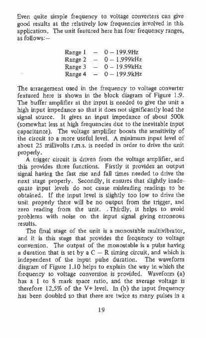
Even quite simple frequency to voltage converters can give good results at the relatively low frequencies involved in this application. The unit featured here has four frequency ranges, as follows:—
Range 1 — O — 199.9Hz Range 2 — O — 1.999kHz Range 3 — O — 19.99kHz Range 4 — O — 199.9kHz
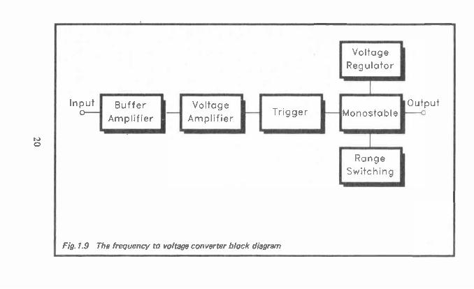
The arrangement used in the frequency to voltage converter featured here is shown in the block diagram of Figure 1.9. The buffer amplifier at the input is needed to give the unit a high input impedance so that it does not significantly load the signal source. It gives an input impedance of about 500k (somewhat less at high frequencies due to the inevitable input capacitance). The voltage amplifier boosts the sensitivity of the circuit to a more useful level. A minimum input level of about 25 millivolts r.m.s. is needed in order to drive the unit properly. A trigger circuit is driven from the voltage amplifier, and
this provides three functions. Firstly it provides an output signal having the fast rise and fall times needed to drive the next stage properly. Secondly, it ensures that slightly inade-quate input levels do not cause misleading readings to be obtained. If the input level is slightly too low to drive the unit properly there will be no output from the trigger, and zero reading from the unit. Thirdly, it helps to avoid problems with noise on the input signal giving erroneous results.
The final stage of the unit is a monostable multivibrator, and it is this stage that provides the frequency to voltage conversion. The output of the monostable is a pulse having a duration that is set by a C — R timing circuit, and which is independent of the input pulse duration. The waveform diagram of Figure 1.10 helps to explain the way in which the frequency to voltage conversion is provided. Waveform (a) has a 1 to 8 mark space ratio, and the average voltage is therefore 12,5% of the V+ level. In (b) the input frequency has been doubled so that there are twice as many pulses in a
19
o
Input o Buffer
Amplifier
Voltage
Amplifier Trigger
Fig. 1.9 The frequency to voltage converter block diagram
Voltage
Regulator
Monostable
1 Range
Switching
Output cfl

V+
OV
V+
OV
V+
OV
- Average Voltage \
(a) _
(b)
C
-
Fig. 1.10 Monostable output waveforms for various input frequencies
given period of time, and the mark space ratio is 1 to 4. This gives an average voltage equal to 25% of the Vi- level. In (c) the input frequency has once again been doubled, taking the mark space ratio to I to 1, and giving an average output voltage that is equal to 50% of the V+ level. The circuit thus provides the required action, with a linear relationship between the input frequency and the average output voltage.
Although strictly speaking the circuit is not a frequency to voltage converter, since the output is a series of pulses and not a d.c. level, all that is needed in order to give a true frequency to voltage conversion is a lowpass filter. This smooths out the pulses to give a low ripple d.c. output potential equal to the average output voltage. In this case there is no need to use a filter at the output of the monostable, since a suitable filter is included at the input of the d.v.m. module.
The monostable must be powered from a stable supply as any change in the supply voltage will be reflected in a propor-tional shift in its average output voltage. Several measuring
21

ranges are provided by using switched resistors in the C — R timing circuit to provide several output pulse durations. This gives the unit four measuring ranges, as follows:—
Range 1 — 0 to 199.9Hz Range 2 — 0 to 1.99kHz Range 3 — 0 to 19.99kHz Range 4 — 0 to 199.9kHz
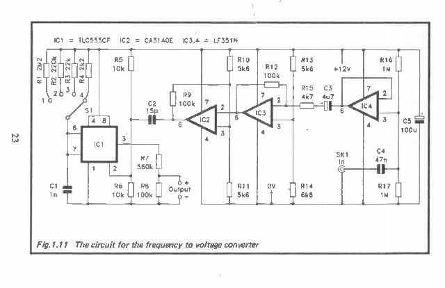
Frequency to Voltage Converter Circuit Figure 1.11 shows the full circuit diagram for the frequency to voltage converter. IC4 is the input buffer stage, and is an operational amplifier used in the non-inverting mode with 100% negative feedback. IC3 provides the voltage amplifica-tion, and this is an inverting mode circuit having an open loop voltage gain of about 26dB (20 times). The trigger circuit is based on IC2, which uses a conventional inverting mode arrangement with hysteresis introduced by R9. Increased hysteresis can be provided by making R9 lower in value. This gives better reliability on signals that contain a lot of noise, but at the cost of reduced sensitivity.
The monostable uses 555 timer ICI in the conventional monostable mode. Actually ICI is a low power version of the 555 timer, the TLC555CP. The output of the interface must be referenced to the negative input terminal of the voltmeter, not the 0 volt supply rail (which is several volts negative of the negative input). This often means that any circuit added ahead of the d.v.m. module must be powered from between the negative input terminal and the positive supply rail. Alternatively, and as in this case, the main circuit can be supplied from the normal supply rails, with only the output stage using the negative input as its 0 volt supply rail. This gives a relatively low supply voltage for the circuit or output stage, and there is the added problem that it must not draw a very high supply current if it is to leave the d.v.m. module functioning accurately. The TLC555CP is therefore a better choice for this application than the standard 555 timer.
22
N.1 4.)
Cl = TLC555CP IC2 = CA3140E IC3.4 = LF351N
2
—1L
4
Si
4 8
R5
10k
IC1
R9
C2 100k 15p
R6
10k
R
560k
R8
100k Output
?
R10
5k6 R12
100k
R11
5k6
OV
R13 R16
5k6 +12V 1M
R15 C3
4k7 4u7
R14
6k8
Ski In
C4
47n
IE-R17
1M
tzt C5 ma
100u
Fig.1.11 The circuit for the frequency to voltage converter
A 555 monostable is of the negative edge retriggerable type, which means that it can only operate as a pulse stretcher. The output pulse can not be shorter in duration than the input pulse at the trigger input. To give the desired action in this application the trigger pulses must therefore be very brief negative spikes. The required pulse shaping is provided by C2 plus the input impedance of R5 and R6. These provide a highpass filter action that gives brief positive spikes on the leading edges of the squarewave input, and negative spikes on the trailing edges. The positive pulses have no effect, but the negative ones trigger ICI. C2 has necessarily been made very low in value, and it is possible that some TLC555CPs will fail to trigger. If this should happen, making C2 a little higher in value should cure the problem, but keep its value as low as possible. The average output voltage from ICI is excessive, but it is attenuated to a suitable level for the d.v.m. module by R7 and R8.
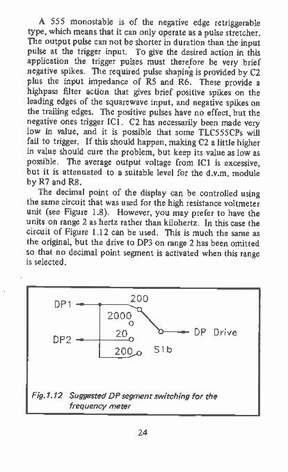
The decimal point of the display can be controlled using the same circuit that was used for the high resistance voltmeter unit (see Figure 1.8). However, you may prefer to have the units on range 2 as hertz rather than kilohertz. In this case the circuit of Figure 1.12 can be used. This is much the same as the original, but the drive to DP3 on range 2 has been omitted so that no decimal point segment is activated when this range is selected.
DP1
DP2
200
2000 o
20
200 S1b
DP Drive
Fig. 1.12 Suggested DP segment switching for the frequency meter
24

Calibration Calibration of any frequency meter can be something of a problem. An accurate frequency within the range of the unit is needed, and it should preferably be a frequency that represents about 50 to 100% of the calibration range's full scale value. If your test equipment includes a crystal cali-brator, this may well be able to provide a suitable calibration signal. Some calibrators only provide frequencies of about 1MHz and higher, but many provide outputs at 100kHz and lower frequencies. A suitable crystal calibrator design is included in Chapter 2 incidentally.
There are other possible sources for calibration frequencies. Television and radio stations often transmit a test tone (usually at 800Hz or 1 kHz) for a while after close down at night. Electronic musical instruments usually have crystal controlled tone generators that have good accuracy. Middle A is at 440Hz, and the A two octaves higher than this is there-tore at a frequency of 1.76kHz. This would seem to be ideal for calibrating the unit on the 2kHz range.
Once you have obtained a suitable calibration signal, simply connect it to the input of the frequency meter, switch the unit to the appropriate range, and then adjust VR1 in the d.v.m. module for the correct reading on the display.
Components for Adujo Frequency Meter (Fig.1.11)
Resistors (0.25 watt 5% unless noted) R1 2M2 1% R2 220k 1% R3 22k 1% R4 2k2 1% R5 10k R6 10k R7 560k R8 100k R9 100k R10 5k6 RI 1 5k6 R12 100k R13 5k6
25

R14 6k8 R15 4k7 R16 1M R17 1M
Capacitors C 1 1 n polyester C2 15p ceramic plate C3 447 63V elect C4 47n polyester C5 100µ 16V elect
Semiconductors IC1 TLC555CP IC2 CA3140E IC3 LF351N IC4 LF351N
Miscellaneous SI 4 way 3 pole rotary (only two poles used) SKI 3.5mm jack socket
8 pin d.i.l. i.c. holder (4 off) D.V.M. module (12 volt version)
Capacitance Meter It is possible to produce a good low cost capacitance meter using a circuit similar to the audio frequency meter unit des-cribed previously, but with a clock oscillator providing the input signal, and the test capacitor forming the capacitive element in the timing network of the monostable. Rather than having a fixed pulse width and a variable repetition rate, this gives a fixed frequency and a variable pulse width. This gives an average output voltage which varies in sympathy with the test capacitance, and which is linearly proportional to it.
An analogue capacitance meter of this type is described in book number BP248, and it would be quite easy to produce a digital equivalent. The problem with this type of capacitance meter is that stray capacitance in the monostable tends to give poor accuracy when testing very low value capacitors. This stray capacitance is usually about 20p to 80p, and seriously
26
degrades accuracy when measuring capacitances of less than a few hundred picofarads. This is not necessarily too important, since low value capacitors are used much less than medium and high value types. On the other hand, if you are interested in radio you are likely to use large numbers of very low value capacitors, and a unit that can check them properly will then be a decided asset.
It is possible to nullify the built-in capacitance of a capaci-tance meter that is based on a monostable, but this is more difficult when feeding the output voltage to a digital voltmeter than it is when using a simple moving coil panel meter. Bridge circuits to null offset voltages are easy using a moving coil meter, but not very practical when using a d.v.m. module. After attempts to produce a good monostable based digital capacitance meter design proved fruitless a different approach was tried, and from this the arrangement shown in the block diagram of Figure 1.13 was developed.
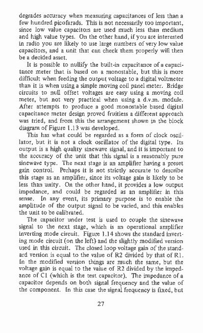
This has what could be regarded as a form of clock oscil-lator, but it is not a clock oscillator of the digital type. Its output is a high quality sinewave signal, and it is important to the accuracy of the unit that this signal is a reasonably pure sinewave type. The next stage is an amplifier having a preset gain control. Perhaps it is not strictly accurate to describe this stage as an amplifier, since its voltage gain is likely to be less than unity. On the other hand, it provides a low output impedance, and could be regarded as an amplifier in this sense. In any event, its primary purpose is to enable the amplitude of the output signal to be varied, and this enables the unit to be calibrated.
The capacitor under test is used to couple the sinewave signal to the next stage, which is an operational amplifier inverting mode circuit. Figure 1.14 shows the standard invert-ing mode circuit (on the left) and the slightly modified version used in this circuit. The closed loop voltage gain of the stand-ard version is equal to the value of R2 divided by that of RI. In the modified version things are much the same, but the voltage gain is equal to the value of R2 divided by the imped-ance of Cl (which is the test capacitor). The impedance of a capacitor depends on both signal frequency and the value of the component. In this case the signal frequency is fixed, but
27

00
Sinewave
Oscillator
Test Cap.
Amplifier
Fig.1.13 The capacitance meter block diagram
Inverting
Amplifier
Precision
Rectifier
Output

In R1 o
Bias
R2
Ouf Cl oHI
O
Bias
R2
Fig.1.14 The capacitance meter is based on an inverting mode amplifier
the capacitance value is not. The impedance value is inversely proportional to the value of the test component.
As a simple example, assume that R2 has a value of 100k, and that the test capacitance has an impedance of 20k. This means that the amplifier will have a voltage gain of five times (100k/20k = 5). If a capacitor having double the value of the original component is connected to the circuit, its impedance will be only half as high (10k as opposed to 20k). This gives an increase in voltage gain to ten times (100k/10k = 10). If a capacitor having half the value of the original component is connected into the circuit, its impedance will be twice as high, and the voltage gain of the amplifier will be half the original figure (100k/40k = 2.5).
It should be apparent from this that the voltage gain of the amplifier is proportional to the value of the test capacitor. It therefore follows that the output voltage from the amplifier will also be proportional to the value of the test capacitor. In order to obtain a capacitance meter action it is merely neces-sary to process the output of the amplifier using a precision rectifier, so that the a.c. signal level is converted to a propor-tional d.c. voltage. This is then fed to the d.v.m. module, and with everything set up correctly the d.v.m. can be made to display the values of test components.
In theory it is not necessary for the signal source to be a highly pure sinewave type. Several component frequencies on the input signal should be satisfactory, since the imper
29

of the test capacitor will be inversely proportional to its value at all frequencies. In practice the frequency response limita-tions of the components in the circuit and possible stability problems must be taken into account. A good quality sine-wave source ensures good results.
This configuration provides excellent results when measur-ing low value capacitors as it has no built-in capacitance to swamp the test capacitance. There will inevitably be a certain amount of stray capacitance, but even with a rather careless layout this is unlikely to total more than a few picofarads. In practice there would seem to be little difficulty in keeping the stray capacitance down to under 1p, and this enables quite good accuracy to be obtained even when testing capacitors having values of just a few tens of picofarads. The unit can be used to make reasonably accurate tests on components having values as low as 10p to 20p.
Although it has definite advantages over more simple types of capacitance measuring circuit, this method is not totally free of drawbacks. One is simply that it is a bit more costly and complex than other methods of capacitance measurement. Another is that it is not strictly speaking capacitance that the circuit responds to, but impedance. If you choose a suitable resistance and connect it across the test socket, the unit will respond with a capacitance value for it. In use this could result in misleading results, but it is not likely to do so. A high leakage and non-functioning capacitor could have a resistance that would give a suitable capacitance reading by sheer chance. However, the chances against this happening must be astro-nomic, and in practice this system gives excellent accuracy, and should give totally reliable results.
The unit described here has five measuring ranges with the following full scale values:—
Range 1 — 1.999n Range 2 — 19.99n Range 3 199.9n Range 4 1.999µ Range 5 — 19.99µ
This covers most requirements, including capacitors of just a
30
few picofarads in value. The accuracy when testing these is not particularly good, since they are effectively measured using a single digit display. Results are good enough to sórt out the good from the bad though, or to check the value of a component if its markings are not entirely clear. At the high end of the range the unit covers all but high value electrolytic components. However, a simple check with a multimeter will usually reveal whether or not a capacitor of this type is serviceable.
The Circuit The circuit diagram for the capacitance meter appears in Figure 1.15. The sinewave "clock" signal is generated by ICI, which is used in a Wien oscillator. This is the type of oscillator circuit that is often used in high quality audio signal generators for their sinewave output, and it is very similar to the sinewave generator section of the A.F. signal generator described in book number BP248. In this case though, the Wien network uses only fixed value components since a single output frequency is needed. The output frequency is quite low, and is in fact close to the lower limit of the audio range. Due to the low operating frequency of the circuit, it could be advan-tageous to make C3 in the d.v.m. module a little higher in value (say 220n).
Th 1 provides thennistor stabilisation of the output level. Apart from ensuring that a highly pure output signal is obtain-ed, this also stabilises the output level. Remember that any changes in the output level will be reflected in variations in capacitance readings, and that a constant output level is therefore essential if the unit is to fulfil its potential accuracy. IC2 is the buffer amplifier, and this is a simple inverting mode circuit with VR1 providing both sections of the negative feedback network. VR1 is, of course, the calibration control.
IC3 is the inverting amplifier which has the test capacitance as its input feedback component. Si is the range switch, and five switched feedback resistors provide the unit with its five measuring ranges. CS couples the output of IC3 to a conven-tional precision rectifier circuit. This is a simple half-wave non-inverting type based on IC4. As explained previously, the lowpass filter at the input of the d.v.m. smooths the pulsating
31

4.1 t•-)
IC1,2,3 = uA741C IC4 = LF441CN D1,2 = 1N4148 o+12V
R1 3k3
R3
47k
C 1 100n
3
R4 1k5
C3 100n
R5 47k
4
R2 C2 I 3k9 7100u
Thl R53
VR1 -" 10k
to* SK1 Cap
—o o
R6 4k7
1 C.,,jr-c.c..4] CV CV CV
I CV 0
P ee.C5 4u7T
C4 R7 4u7J 5k6
6 Si
N_J
R13 10k
1
R14 10k 1--6-0 — In
Fig.1.15 The capacitance meter circuit diagram
02

DP3
DP2
DP1 DP Drive
Fig. 1.16 The suggested decimal point switching for the capacitance meter
d.c. output of the unit, giving a reasonably ripple-free signal that the voltmeter can measure properly.
Suitable decimal point switching for the capacitance meter unit is shown in Figure 1.16. This provides readings in nano-farads on ranges 1 to 3, and readings in microfarads on ranges 4 and 5.
Calibration Construction of the unit should not present any major diffi-culties. The layout is not particularly critical, but you should obviously choose one that puts a minimum of stray capaci-tance in parallel with SK1. Do not use a screened lead or separate leads twisted together to make the connections between SKI and the circuit board. Use individual leads kept as far apart as possible. Something like individual 2 milli-metre sockets or a twin spring-loaded terminal panel might be a better choice for SKI than a single two way socket, giving lower stray capacitance. I used a twin spring-loaded terminal unit on the prototype. Many capacitors can be clipped direct to this quite easily. For those that will not connect to it properly a set of test leads must be made up. These should be as short as is practical, so that their self-capacitance is mini-mised. They are fitted with miniature crocodile clips, which will permit easy connection to any normal type of capacitor.
33

It will probably not be possible to obtain a five way rotary switch for Sl, but a 6 pole 2 way type having an adjustable end-stop (set for five way operation of course) is perfectly suitable. R8 to R12 must all be close tolerance (1% or better) components in order to ensure good accuracy on all ranges. The thermistor used in the Thl position of the circuit is a special self-heating type in a glass encapsulation. It seems to be available as either an R53 or an RA53. Either type should be perfectly suitable for operation in this circuit, but other types are unlikely to give usable results.
Before calibrating the unit the d.v.m. module should be set for a full scale sensitivity of about 200 millivolts. One way of doing this is to connect its input to the circuit of Figure 1.17. This uses a 9 volt battery as the signal source, plus a simple attenuator to reduce the output level to roughly 200 milli-volts. This will not provide particularly accurate results, but it is only necessary for the d.v.m. sensitivity to be roughly 200 millivolts full scale. It is VR1 in the capacitance meter add-on circuit that is used for precise calibration of the unit.
In order to calibrate the unit a close tolerance capacitor is needed, and this should have a value which represents about 50 to 100% of the full scale value of one of the capacitance
R1 10k
B1
9V
R2 220
Output
Fig.1.17 A simple circuit to provide a 200mV calibration voltage
34

meter's ranges. If you do not have a suitable component in the spares box and have to buy one specially, then it is probably best to calibrate the unit on range 1. A in or 1.5n 1% capacitor will then suffice, and a close tolerance compon-ent at either of these relatively low values should not be very expensive. Simply switch the unit to the appropriate range, connect the test capacitor, and then adjust VR1 in the capaci-tance meter add-on for the correct reading on the display. The unit should then give accurate results on all five ranges.
When using any capacitance meter there are a few points that should be kept in mind. Firstly, do not connect a charged capacitor to the unit. If the capacitor has only a low voltage charge, then this is unlikely to do any damage. However, charges of more than a few volts, particularly when measuring higher value components, could easily damage the circuit. You may like to add a couple of sockets to the front panel of the unit, with a resistor of about 47 oluris connected between them. Test components can then be connected across these sockets and discharged prior to being measured.
When testing capacitors you should bear in mind that they often have quite wide tolerances. With some of the smaller types the tolerance is around 1% to 5%, but most capacitors have tolerances of 10% or 20%. Certain types commonly have even wider tolerances. In particular, disk ceramic and electrolytic types often have tolerances of about plus 50% and minus 20%, and I have encountered electrolytic capacitors with tolerances of plus 100% and minus 50%. Therefore, if readings sometimes differ quite significantly from the marked values of components, this does not necessarily mean that the components in question are "duds". The discrepancies could be due to the wide tolerances of the test components. When testing close tolerance components, remember that the basic accuracy of the capacitance meter unit is about plus and minus 1% or so, and that an error of about 2% on a 1% component does not necessarily mean that it is outside its specification.
In theory the unit is not suitable for testing electrolytic components since there is no significant d.c. bias across the test socket. In practice there will be a small d.c. bias present here, and connecting electrolytic capacitors one way round or the other should give satisfactory results. A little
35
experimentation should reveal the correct polarity for polar-ised capacitors (in practice it is quite likely that connecting them with either polarity will give satisfactory results).
Components for Capacitance Meter (Fig.1.15)
Resistors (0.25 watt 5% unless noted) R1 3k3 R2 3k9 R3 47k R4 1k5 R5 47k R6 4k7 R7 5k6 R8 2M2 1% R9 220k 1% R10 22k 1% RII 2k2 1% R12 22OR 1% R13 10k R14 10k R15 10k
Capacitors C 1 100n polyester C2 10012 10V elect C3 100n polyester C4 4µ7 63V elect C5 427 63V elect
Semiconductors IC1 p.A7 41C IC2 j./A741C IC3 A741C IC4 LF441C D1 1N4148 D2 1N4148
Miscellaneous S1 5 way 2 pole rotary (6 way with adjustable
end-stop)
36
SKI See text Th 1 R53 or RA53 thermistor
8 pin d.i.l. i.c. holder (4 off) d.v.m. module (12 volt version)
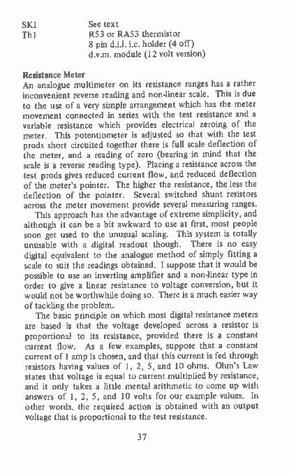
Resistance Meter An analogue multimeter on its resistance ranges has a rather inconvenient reverse reading and non-linear scale. This is due to the use of a very simple arrangement which has the meter movement connected in series with the test resistance and a variable resistance which provides electrical zeroing of the meter. This potentiometer is adjusted so that with the test prods short circuited together there is full scale deflection of the meter, and a reading of zero (bearing in mind that the scale is a reverse reading type). Placing a resistance across the test prods gives reduced current flow, and reduced deflection of the meter's pointer. The higher the resistance, the less the deflection of the pointer. Several switched shunt resistors across the meter movement provide several measuring ranges.
This approach has the advantage of extreme simplicity, and although it can be a bit awkward to use at first, most people soon get used to the unusual scaling. This system is totally unusable with a digital readout though. There is no easy digital equivalent to the analogue method of simply fitting a scale to suit the readings obtained. I suppose that it would be possible to use an inverting amplifier and a non-linear type in order to give a linear resistance to voltage conversion, but it would not be worthwhile doing so. There is a much easier way of tackling the problem.
The basic principle on which most digital resistance meters are based is that the voltage developed across a resistor is proportional to its resistance, provided there is a constant current flow. As a few examples, suppose that a constant current of 1 amp is chosen, and that this current is fed through resistors having values of 1, 2, 5, and 10 ohms. Ohm's Law states that voltage is equal to current multiplied by resistance, and it only takes a little mental arithmetic to come up with answers of 1, 2, 5, and 10 volts for our example values. In other words, the required action is obtained with an output voltage that is proportional to the test resistance.
37

Therefore, a linear resistance meter interface for a volt-meter only needs to be a simple setup of the type outlined in Figure 1.18. The test resistor is fed from a constant current generator circuit, and if several measuring ranges are needed, this must have several switched output currents. The buffer amplifier ensures that no significant current is tapped off by the voltmeter connected to the output. This prevents the voltmeter circuit from shunting the test resistor, and possibly preventing the system from operating properly. Clearly it would not be possible to measure resistors having values of a few megohms if the voltmeter placed a resistance of a few kilohms across the test points. In this case the buffer amplifier is not required because the d.v.m. module has an exceedingly high input resistance. However, if you should try to use the resistance meter circuit with another voltmeter you might need to add a buffer amplifier in order to obtain satisfactory results.
38
The Circuit The circuit diagram for the resistance meter is shown in Figure 1.19. This is basically just a conventional constant current generator circuit of the type which has two diodes to provide a bias of about 1.2 volts to the base of a transistor. Due to the voltage drop of about 0.6 volts from the base to the emitter terminals, this gives about 0.6 volts across the emitter resistor. The collector current of a transistor is virtually identical to the emitter current, and the collector current can therefore be set at the required level by using a suitable emitter resis-tance. In this case there are five switched emitter resistances, giving the unit five measuring ranges. The full scale values are as follows:—
Range 1 199.9 ohms Range 2 1.999k Range 3 — 19.99k Range 4 199.9k Range 5 1.999M
Very high value resistors are outside the scope of the unit, but these are little used in practice. At the other end of the range the unit is very good, with a resolution of 100 milliohms on the lowest range.
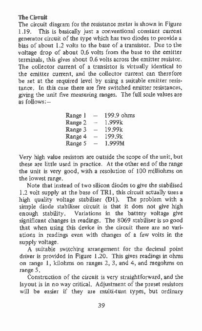
Note that instead of two silicon diodes to give the stabilised 1.2 volt supply at the base of TRI, this circuit actually uses a high quality voltage stabiliser (Dl). The problem with a simple diode stabiliser circuit is that it does not give high enough stability. Variations in the battery voltage give significant changes in readings. The 8069 stabiliser is so good that when using this device in the circuit there are no vari-ations in readings even with changes of a few volts in the supply voltage. A suitable switching arrangement for the decimal point
driver is provided in Figure 1.20. This gives readings in ohms on range 1, kilohms on ranges 2, 3, and 4, and megohms on range 5.
Construction of the circuit is very straightforward, and the layout is in no way critical. Adjustment of the preset resistors will be easier if they are multi-turn types, but ordinary
39
VR1 220
T. R3 1k5
VR2 22k
-(2) ,
VR3 220k
/4/ e 5
_i_
T.
VR4 I- 2M2
ITI 01 ek 8069 si
Range R2 33
R1 10k
TR1 BC559
et. SK1
Test Resistor
SK2
11
Fig. 1.19 The resistance meter circuit diagram
0 +9V
o In
DP1
DP3
DP2 DP Drive
Fig. 1.20 Suggested decimal point switching for the resistance meter
40

miniature presets are just about usable. The unit requires the d.v.m. module to have a somewhat higher full scale input voltage than that needed by the other circuits. It might not be possible to obtain a suitable sensitivity with the original component values, but increasing VR1 from lk to 10k should ensure that the unit can be calibrated correctly.
Calibration requires five close tolerance resistors having values at something approaching the full scale value of each of the five measuring ranges. The best values to use are therefore 180 ohms, 1k8, 18k, 180k and 1M8 to calibrate ranges 1 to 5 respectively. Close tolerance resistors having values of more than 1 megohrn are relatively difficult to obtain and expensive. Accordingly, you might prefer to use a 1M component to calibrate range 3.
Start by switching the unit to range 2 and connecting the 1k8 resistor across SK1 and SK2. Next adjust VR1 in the d.v.m. module for a reading of "1.800". Then connect the 180 ohm resistor across SKI and SK2, switch the unit to range 1, and adjust VR1 in the resistance meter circuit for a reading of "180.0". Repeat this general procedure using the 18k, 180k and 1M8 resistors to calibrate ranges 3 to 5 respectively, with VR2 to VR4 being used to set the correct readings for their respective ranges. The unit is then ready for use.
• Components for Resistance Meter (Fig.1.19)
Resistors (all 0.25 watt 5%) R I I Ok R2 33R R3 1k5
Potentiometers VR1 VR2 VR3 VR4
Semiconductors Dl TRI
22OR multi-turn preset 22k multi-turn preset 220k multi-turn preset 2M2 multi-turn preset
8069 1V2 reference voltage generator BC559
41
Miscellaneous SK1 SK2 SI
2mm socket 2mm socket 5 way 2 pole rotary (6 way 2 pole with adjustable end-stop) 180R, 1k8, 18k, 180k, and 1M8 1% toler-ance resistors for calibration purposes.
Transistor Tester Comprehensive transistor testers are highly complex pieces of equipment that enable the test parameters (collector voltage, collector current, etc.) to be set at practically any desired levels. For most purposes though, a unit of this type is severely over-specified. Generally what is needed is a device that will give an indication of current gain for both n.p.n. and p.n.p. devices, and which can be used quickly and easily without the need for any complex setting up procedures. The fact that the test conditions are not the same as those specified in the data sheet for the component under test does not matter too much. These differences can be taken into account when assessing results.
Probably the two most important test conditions are the collector current and the collector voltage. In general, the gain of a transistor rises slightly as the collector voltage is increased. The difference is usually quite small even with substantial changes in the collector potential, and this is unlikely to be the cause of significant anomalies provided the collector volt-age is not allowed to become very low. The collector current is a different matter though. The gain of a transistor, in the main, rises as its collector current is increased. The difference in gain can be quite dramatic. A transistor that has a current gain of a few hundred times at a collector current of one milliamp might have a gain of less than ten times at a collector current of ten microamps. Differences between the collector current at which a transistor's gain is specified in the data sheet, and the actual current at which it measured, must therefore be taken into account when assessing results.
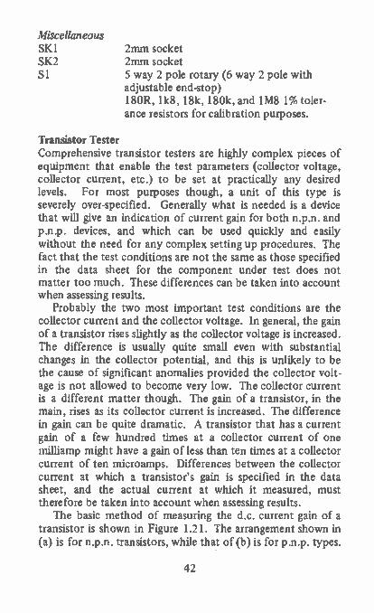
The basic method of measuring the d.c. current gain of a transistor is shown in Figure 1.21. The arrangement shown in (a) is for n.p.n. transistors, while that of (b) is for p.n.p. types.
42
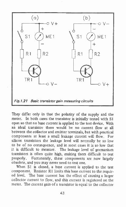
Fig. 1.21 Basic transistor gain measuring circuits
They differ only in that the polarity of the supply and the meter. In both cases the transistor is initially tested with Si open so that no base current is applied to the test device. With an ideal transistor there would be no current flow at all between the collector and emitter terminals, but with practical components at least a small leakage current will flow. For silicon transistors the leakage level will normally be so low to be of no consequence, and in most cases it is so low that it is difficult to measure. The leakage level of germanium transistors is often quite high, making them difficult to test properly. Fortunately, these components are now largely obsolete, and you may never need to test one.
When Si is closed, a base current is applied to the test component. Resistor R1 limits this base current to the requir-ed level. The base current has the effect of causing a larger collector current to flow, and this current is registered on the meter. The current gain of a transistor is equal to the collector
43

current divided by the base current. Here we are assuming that the leakage is so low that it does not need to be taken into account (which will almost invariably be the case in practice). There is a linear relationship between the gain of the transistor and the meter reading, making it an easy matter to arrange for the meter to give a direct readout of the current gain.
The Circuit Refer to Figure 1.22 for the full circuit diagram of the transistor tester. Devising a circuit for testing p.n.p. devices presents no real problems. The emitter terminal is switched through to the positive supply rail, the base resistor is connec-ted to the negative supply rail, and the d.v.m. module is used to measure the collector current. Although the d.v.m. module is designed for voltage measurement, it is easily converted to current measurement. It is just a matter of connecting a shunt resistor across its input. In this case the shunt resistance is the parallel resistance of R3 and R4, which is some 50 ohms. With the d.v.m. module having a full scale value of 200 milli-volts, this effectively converts it to a current meter having a full scale value of 4 milliamps (0.2 volts divided by 50 ohms equals 0.004 amps or 4 milliamps). . Base resistor R5 provides a base current of approximately 2 microamps. Therefore, if the test transistor has a gain of one thousand times it will produce a collector current of 2 milliamps, and will give half full scale value on the d.v.m. module. In other words, a reading of "1000". A current gain of 500 would give a collector current of I milliamp, and a 25% of full scale reading from the d.v.m. module (i.e. a reading of "500"). In other words, the circuit provides readings direct in current gain.
Testing p.n.p. transistors poses no problems, since they act as a current source that can directly drive the d.v.m. module. The same is not true of n.p.n. transistors which act as current sinks, and must drive the d.v.m. module via some form of inverter circuit. This inverting action is obtained using a simple current mirror based on TRI and TR2. The current fed into the base of TR2 produces an almost identical current to be sourced from its collector. For good results the gains of
44
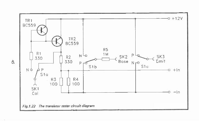
4 LA
TR1 and TR2 should be reasonably well matched. Obtaining ready-matched transistors could be difficult. One solution to the problem is to buy a few BC559s (which are not expensive), and to initially use any two of them for TRI and TR2. Then use the tester to check the others so that the two with the most closely matched gains can be sorted out. These are then used as TR1 and TR2, replacing those originally used in the circuit.
The n.p.n./p.n.p. switching is quite straightforward, with Sla switching the collector test socket (SKI) between the input of the d.v.m. module and the input of the current mirror. RI and R2 are included to protect the unit and devices under test from excessive current flows. There is no need to switch the current mirror out of circuit in the p.n.p. mode, since it will produce only minute leakage currents that are totally inconsequential. SI b switches the base current to the appropriate polarity, while Sic connects the emitter socket (SK3) to the appropriate supply rail.
With a resolution of one the circuit is capable of testing low gain transistors. However, the collector current at which devices are tested becomes very small if they have low current gains. For instance, a transistor with a current gain of 500 will be tested at a collector current of 1 milliamp, but one which has a gain of 50 will be tested at a current of only 100 microamps. This can give what are really artificially low gain readings on lower gain devices, possibly resulting in very mis-leading results. This is not a major problem if you take into account that low gain devices will be measured at low collector currents. However, you may prefer to add a second measuring range having a full scale value of 199.9 (as opposed to the 1999 of the original circuit). This merely entails adding a d.p.d.t. switch and a 100k resistor, as shown in Figure 1.23. Selecting the 100k resistor instead of the 1M component boosts the base current to approximately 20 microamps. The test devices then only need one-tenth of the current gain in order to produce a given collector current and reading. The second pole of S2 is used to connect the DP drive signal through to the DPI pin of the liquid crystal display, so that the appropriate decimal point segment is switched on when the additional range is used.
46

R5 1 M
To S1 b Pole
DP Drive
SK2 Base
S2b
(1"---0--- DP1
Fig. 1.23 Adding a second range to the transistor tester
Construction of the transistor tester should be very simple, and there is nothing critical about the layout. SKI to SK3 should be miniature (1 or 2 millimetre) sockets mounted close together. Most transistors will then plug directly into them without too much difficulty. Clearly label the sockets and (or) use sockets of different colours to permit easy identifica-tion, and reduce the risk of connecting test devices incorrectly (something which is unlikely to damage the transistors or the tester). Some transistors will not easily connect to the sockets, and for these a set of test leads terminated in crocodile clips must be made up. Use leads and (or) clips of different colours so that the leads are easily identified and errors are avoided when connecting test components.
Unlike construction of the unit, calibration does pose something of a problem, but if you have the necessary test equipment it is possible to measure the exact base current and adjust the sensitivity of the d.v.m. module to suit. In practice this would not really seem to be worthwhile. As pointed out previously, results have to be considered subjectively since measurements are not being made at user selected collector currents and voltages. However carefully the unit is calibrated,
47
results will always lack true precision. A simple but adequate means of calibrating the unit is to connect a 1k2 resistor between the positive supply rail and the "+In" terminal of the d.v.m. module. Then adjust VR1 in the d.v.m. module for a reading of "1000". The unit is then ready for use, and should give reasonably accurate results.
When using the unit you should initially connect only the collector and emitter terminals each time you test a transistor. This enables a test for leakage to be made prior to connecting the base terminal and taking a gain measurement. You may prefer to add a switch to permit the base current to be switched on and off, but I found it easier to simply connect the base lead or leave it unconnected, as required. For silicon transistors there should be extremely low leakage currents which in most cases will be too low to register on the d.v.m. module. With germanium transistors quite high leakage currents are often tolerable. To obtain a meaningful current gain figure when there is a high leakage level you must deduct the leakage current reading from the current gain reading.
Components for Transistor Tester (Fig.1.22)
Resistors (all 0.25 watt 5%) R1 330R R2 330R R3 100R R4 100R R5 1M
Semiconductors TR1 T R2
Miscellaneous SI
SKI SK2 SK3
BC559 BC559
2 way 3 pole (e.g. 4 way 3 pole rotary switch having an adjustable end-stop set for 2 way operation) 2mm socket 2mm socket 2mm socket d.v.m. module (12 volt version)
48

Current Tracer A current tracer is a device for testing the current flow through printed circuit tracks and component wires. Normally the measurement of current through either of these requires that the lead or track should be cut so that the current meter can be wired into the signal path. This is obviously time consum-ing, and rather destructive. Tracks can be repaired, and component leads can be joined together again, but this type of thing can soon reduce a neat circuit board to a piece of junk! Testing of this kind therefore has to be avoided as far as possible, which usually means largely or totally abandoning current checks in favour of voltage tests. This can make life difficult, since detecting an incorrect current flow into a stage of a circuit would often represent the quickest means of detecting the faulty part of a circuit. It can be particularly useful with circuits that contain a number of integrated circuits and few discrete components, as these are often very difficult to test properly using voltage checks.
There are some quite sophisticated pieces of electronics which enable the current flow through a track or wire to be measured quite accurately without actually breaking the circuit and inserting a meter. One system uses a special Hall Effect device to detect the strength of the magnetic field produced by the current flow, and from this the amount of current flow can be determined with reasonable accuracy. As yet, this system is probably not a practical proposition for the home constructor as it is fairly com-plex, and suitable Hall Effect sensors for this particular application would not seem to be available to the home constructor.
There is a much more simple alternative which is less accurate, but which can provide some useful results. This is really a variation on the standard current measuring tech-nique. Figure 1.24(a) shows the basic setup for current measurement. The current is passed through resistor R1 and meter ME1. The current is split between the two of them, and the lower R1 is made in value, the greater its share of the current flow. RI therefore enables the full scale current of the circuit to be set at any figure higher than the basic sensitivity of the meter.
49

(a)
R1 R1
Fig. 1.24 (a) A conventional current meter circuit, and (b) the arrangement used in the current tracer. It is really just a highly sensitive current meter
The arrangement shown in Figure 1.24(b) is similar, but a high gain d.c. amplifier has been added between the shunt resistor and the voltmeter circuit. This has the effect of making the circuit extremely sensitive, being able to readily detect currents into the nanoamp region. If the input of the circuit is connected across a short piece of track or a length of leadout wire, some of the current flowing in that wire or track will flow through RI and will be registered on the meter. With the leadout wire or track having a very low resistance in comparison to R1 the proportion of the total current flow that will be redirected through R1 is likely to be extremely small. However, provided the amplifier is sufficiently sensi-tive, this current will be detected and indicated by the meter. The percentage of current that the unit redirects will remain the same regardless of the actual current flow through the wire or track. Therefore, the greater the current flow, the greater the reading on the meter.
This method lacks precision in that the proportion of current that the tracer unit will redirect is dependent on several factors. One is simply the distance between the test prods. The greater this distance, the higher the track or lead resistance between i them, and the greater the proportion of current that the unit will tap off. Using a fixed amount of
50
separation can help to give more meaningful results, but does not totally solve the problem. The resistance per millimetre of track or lead will vary, and will be more for thin leads or tracks. The quality of the connection between the test prods and the test points can also have a significant effect on readings.
Consequently, this method of current tracing does not give highly accurate results. It does give a good guide to the amount of current going through a track though. Often a fault will result in a stage consuming a current several times higher than its normal level, or only a fraction of its normal level. These large discrepancies are readily detected using even a simple current tracer of this type. It is the type of thing where experience counts for a great deal, and it is a good idea to use the unit to prod around on some functioning circuits, getting used to the sorts of readings that various levels of current flow produce. You will then quickly spot any readings that are inappropriate for the correct current flow.
The Circuit Figure 1.25 shows the circuit diagram for the current tracer. This is just a standard operational amplifier inverting mode circuit. The closed loop voltage gain is set by RI and R2 at a little over 46dB (200 times), and together with the low full scale value of the d.v.m. circuit, this gives excellent sensitivity.
VR1 is an offset null control. With a theoretically perfect operational- amplifier this is unnecessary, but with practical devices the input and output voltages can drift away from the correct levels. This problem can be quite acute in a circuit of this type which has quite a high d.c. voltage gain. In fact the input offsets when multiplied by the closed loop voltage gain of the amplifier can be so high that the output of the amplifier simply goes fully negative or fully positive under quiescent conditions! VR1 enables any offset voltages to be trimmed out so that zero output voltage is produced under standby conditions.
The unit should not prove to be difficult to construct. IC1 has quite a high voltage gain, but due to its low input imped-ance and the fact that its input and output are out-of-phase, instability is unlikely to occur. It is advisable to use a multi-
51

o +12V ICI = uA74IC
R1
47
o—H Input o
2
3
7
5
R2
10k
6
4 o +In
VR1
1 Ok
Fig. 1.25 The current tracer circuit diagram
In
o OV
turn preset for VR1. Adjustment of this control is very critical, and it might not be possible to accurately trim out the offset voltages if an ordinary preset resistor is used in the VR1 position. When the unit is first switched on it is unlikely that any offsets will be apparent. The reason for this is that ICI is used in the inverting mode, and there is effectively 100% negative feedback through R2 (and only unity voltage gain) when the input is open circuit. Short circuiting the test prods together will almost certainly produce a large change in the output voltage, probably resulting in an overload indication from the d.v.m. module. By carefully adjusting VR1 it should be possible to trim the output voltage down to zero, and it should remain at zero when the short circuit across the test prods is removed. Note that with this particular pro-ject the setting of VR1 in the d.v.m. module is not particularly
52

important. Any setting that gives good results can be used, and virtually any setting of VR1 will probably fall in this category.
As pointed out previously, interpreting results with a unit of this type is something that can only be based on practical experience. You therefore need to experiment a little with the unit before trying to use it in earnest. It will detect quite small current flows, but if there is only a microamp or two flowing through a printed circuit track, it would be unrealistic to expect a unit of this type to detect it. The polarity indica-tor on the display will show the polarity of the input signal, but bear in mind that the unit can not detect a.c. current flows. It detects the average current flow if the input signal is not a constant d.c. type. The average current in an a.c. signal is zero, with the positive half cycles cancelling out the negative ones. This is not a major drawback in practice since few circuits contain true a.c. current flows. They are mostly constant or pulsing d.c. types, both of which the current tracer unit can detect properly.
Components for Current Tracer (Fig.1.25)
Resistors (all 0.25 watt 5%) R1 47R R2 10k
Potentiometer VR1 10k multi-turn preset
Semiconductor IC1 µA741C
Miscellaneous 8 pin d.i.l. i.c. holder d.v.m. module (12 volt version)
Heatsink Thermometer When dealing with semiconductors operating at high power levels there is the ever present danger of overheating occurring. If the thermal conduction between a semiconductor and its
53

Vt 4
o +9V R1 22k _
R2 100k _
r— i cl "." 47u
6
7
4 8
IC1 3
TLC555CP
2
D1 Z1N4148
m,
04 4u7
C3 02 4u7 1N4148
V+ IO2
LM35DZ
-
R3 Out 820k --1 I t o +In
R4 100k
Fig. 1.26 The heatsink thermometer circuit diagram
In
o OV

heatsink is not all it could be, you are not likely to become aware of the fact until the device becomes excessively hot and breaks down. This can be spectacular, and more than slightly dangerous. Overheating semiconductors have a nasty habit of exploding with a loud "crack", with bits of plastic, etc. flying in all directions! A thermometer can be more than a little helpful when
checking that power circuits are operating within their designed temperature limits. You can check that devices are operating at suitable temperatures, and do something about it before it is too late if an excessive temperature is detected. By measuring the difference between the case and heatsink temperatures you can get a good idea of how efficiently (or otherwise) the power device is transferring its heat to the heatsink.
Obtaining a thermometer action from the d.v.m. module is quite simple, either using a discrete temperature sensor based on a diode sensor, or using a special integrated circuit which also utilizes what is essentially a diode sensor. The basic method of using a diode as a temperature sensor is to forward bias it from a constant current source. The voltage developed across a forward' biased silicon junction is about 0.65 volts, but this figure varies with temperature. The change is a reduc-tion of only about 2 or 3 millivolts per degree Celsius increase, but this is sufficient for many purposes and can easily be amplified if necessary. The advantage of semiconductor sensors over other simple forms of temperature sensor is that they provide good linearity over a wide temperature range.
The circuit (Figure 1.26) of this thermometer is based on a special temperature sensor integrated circuit, the LM35DZ (IC2). This provides an output voltage equal to 10 milli-volts per degree Celsius over the range 0 to 100 degrees Celsius. This makes it well suited to the current application where the temperature range of main interest is around 40 to 100 degrees Celsius. Accuracy at low temperatures is not very good, but this is clearly of no consequence in the current application. The output of IC2 is about ten times higher than is needed to drive the d.v.m. module, and so R3 and R4 are used to attenuate its output to a suitable level. The DP drive signal should be connected through to the "DP1" segment of
55

the liquid crystal display. The d.v.m. module can then be set-up to give readings from 0 to 100.0 degrees Celsius. Although the display can go as high as 199.9 degrees Celsius, the• accuracy of readings over 100 degrees can not be guaran-teed, and there is a risk of the sensor being damaged by overheating.
One slight problem is that the LM35DZ requires a mini-mum supply voltage of 4 volts, but the potential from the "—In" terminal to the positive supply rail is a volt or so less than this. IC1 is therefore used as an oscillator driving a smoothing and rectifier circuit which provides a potential of about +8 volts referenced to the positive supply rail. This is used as the positive supply rail for IC2, and gives it a total supply voltage of about 10 volts. Changes in battery voltage result in significant variations in the supply voltage to the LM35DZ. This does not matter though, as this device has built-in stabiliser circuits which render changes in the supply voltage innocuous.
Construction presents nothing out of the ordinary apart from the fact that the sensor is not mounted on the circuit board. Instead it is connected to the rest of the unit via a three way lead about half a metre or so in length. Ideally the cable should be a twin screened type with the outer braiding carrying the connection to the "V—" terminal of IC2. With a little initiative it should be possible to make the sensor into a neat probe assembly. This is not essential though, and the main point to watch is that IC2's leads are properly insulated from one another so that short circuits are avoided.
Calibration requires the sensor to be subjected to a known temperature. VR1 in the d.v.m. module is then adjusted to produce the appropriate reading on the display. In order to calibrate the unit you will need a thermometer against which it can be set up. There is no need for any elaborate proced-ures. Measure the room temperature using the calibration thermometer, and then simply adjust VR1 in the d.v.m. module to give the same reading on the liquid crystal display. It obviously helps if the calibration thermometer is a good quality type which offers good accuracy. It is also preferable if the unit is calibrated at a reasonably high temperature. One at about 20 to 25 degrees is better than about 10 to 15 degrees,
56
where the unit is likely to offer slightly lower accuracy. When using the unit bear in mind that it takes at least a few
seconds for the sensor to adjust to new temperatures. In fact it could take as much as a minute or two for it to fully adjust to very large changes in temperature.
Components for Heatsink Thermometer (Fig. ).26)
Resistors (all 0.25 watt 5%) RI 22k R2 100k R3 820k R4 100k
Capacitors CI C2 C3 C4
Semiconductors IC1 IC2 D1 D2
Miscellaneous
47µ 16V elect 1 n polyester 4µ7 63V elect 4117 63V elect
TLC555CP LM35DZ 1N4148 1N4148
8 pin d.i.l. i.c. holder Twin screened lead
Mains PSU The projects described in this chapter are all suitable for battery operation, but they can obviously be built as mains powered units if preferred. The mains power supply circuit of Figure 1.27 is suitable as the power source for all the projects featured in this chapter. It has full wave bridge rectification, smoothing provided by Cl, and stabilisation and further smoothing provided by ICI. It provides a well stabi-lised 12 volt output. Note that where a 9 volt supply has been
57

S1a On/Off
L 0 sr>
240V
Mains
N 4CD
Sib On/Off
E 0
240
Ti
12
Fig. 1.27 The 12 volt mains p.s.u. circuit
IC1 = uA78L12
D1 To D4 = 1N4002
IC1 Out
Corn
11_6 C3 100n
C2 100n 4-1111
l000u
+12V
0 OV

specified for projects it is quite in order to use a 12 volt supply.
Construction of the power supply is in most respects quite simple, but as the mains supply is involved it is important to take due care. Mistakes could prove costly and are potentially very dangerous. The unit must be housed in a case which has a screw fitting lid rather than a lid or cover which simply un-clips. This prevents easy access to the dangerous mains wiring. Any exposed metalwork must be earthed to the mains earth lead, and this includes such things as fixing screws and sockets. In practice the best solution to this problem is usually to use a case of all metal construction. If the case is earthed to the mains earth lead, then any screws, etc. fitted on it will be earthed as well. C2 and C3 are needed to aid the stability of IC1, and they should be mounted as close to ICI as reasonably possible.
Components for 12V Mains PSU (Fig.1.27)
Capacitors Cl 1000µ 25V elect C2 100n ceramic C3 100n ceramic
Semiconductors IC! A78L12 (12 volt 100mA positive regulator) DI 1N4002 D2 1N4002 D3 1N4002 D4 1N4002
Miscellaneous Ti Mains primary, 12 volt 100mA secondary Si Rotary mains switch
Mains lead and plug
59

60

Chapter 2
MISCELLANEOUS TEST GEAR PROJECTS
About the only feature that the projects described in this chapter have in common is that they all make very useful additions to the electronics workshop. Whereas the projects in the previous chapter were concerned with measurements, the projects in this chapter are mainly concerned with the generation of signals of one kind or another. The exception is the final project, which is an unusual but useful form of transistor tester.
Crystal Calibrator For an electronics hobbyist who is interested in radio, particu-larly short wave radio, an r.f. signal generator is a more than slightly useful piece of test equipment. A unit of this type does not need to be particularly complex, and is basically just a multi-range r.f. oscillator plus a buffer amplifier. There is a severe difficulty with a home constructed r.f. signal generator, which is the problem of getting the finished unit accurately calibrated. Even if you have access to suitable test equipment, such as a d.f.m. or an accurately calibrated radio that covers the appropriate frequency range, marking large numbers of calibration points on the dial with adequate accuracy is a difficult and extremely time consuming business. A more simple alternative is to opt for a crystal calibrator.
This can not replace a signal generator in every situation, but it will often do what is required. In some cases it will provide better results than a simple r.f. signal generator, since its frequency accuracy and stability are likely to be vastly superior to a simple r.f. generator design. In its most simple form a crystal calibrator merely consists of a crystal oscillator operating at a useful calibration frequency. This would typically be 1MHz. Although a unit which provides an output at just one frequency, albeit with great accuracy, might not seem to be particularly useful, the salient point here is that the unit is designed to generate strong harmonics at frequencies up to and beyond the 30MHz upper limit of the short wave
61

range. Although the basic output frequency may be 1MHz, there are also signals at 2MHz, 3MHz, 4MHz, 5MHz, etc.
Modern crystal calibrators almost invariably offer a number of fundamental output frequencies. The unit featured here offers outputs at 10MHz, 5MHz, 1MHz, 100kHz, and 10kHz. On the face of it, the higher frequencies are unnecessary as they only provide signals at frequencies that are also present on the lower frequency outputs. For instance, the second harmonic of 10MHz is 20MHz, but a 20MHz signal is also provided by the fourth harmonic of the 5MHz output, the twentieth harmonic of the 1MHz output, the two hundredth harmonic of the 100kHz output, and the two thousandth harmonic of the 10kHz output.
In practice matters are not as simple and straightforward as this. You may well be able to obtain a 20MHz signal from the 10kHz output, but with signals at just 10kHz intervals it would probably be impossible to tell which harmonic is which. This problem can be solved by using the 10MHz signal to give the required 20MHz signal. With the harmonics spaced some 10MHz apart there should be no difficulty in sorting out one harmonic from another, even when testing an uncalibrated receiver.
Suppose that you do not require a frequency as convenient as 10MHz. A frequency such as 11.21MHz would seem to be difficult to locate accurately. In practice a frequency of this type is quite easy to set on the receiver. First use the 10MHz signal and locate it on the receiver. Then switch to the 1MHz signal and tune the receiver higher in frequency until a harmonic is located. This signal will be the first 1MHz harmonic at a frequency above 10MHz, and will obviously be the eleventh harmonic at 11MHz. Next switch to the 100kHz signal, and tune the receiver higher in frequency, going through the first signal (11.1MHz) and on to the next one, which will be at 11.2MHz. Finally, switch to the 10kHz signal, and tune the receiver higher in frequency until the next harmonic is located. This will be at the desired frequency of 11.21MHz.
Using this system it is possible to accurately locate any required frequency that is a multiple of 10kHz. It may take a little while to get there, but provided the procedure is carried
62
out carefully, excellent accuracy can be obtained. It is only fair to point out that some receivers have quite wide band-widths, and it may be difficult to use the unit on its 10kHz output with a set of this type. However, most receivers can use the 10kHz output without any difficulty, and even with a wide bandwidth set the 10kHz output should just about be usable.
The Circuit In days gone by, the standard method of obtaining several output frequencies from a crystal calibrator was to have several crystal oscillators, with switching to select the output from the desired oscillator. This was an extremely expensive way of tackling the problem, bearing in mind the extremely high cost of crystals in those days. Crystals cost very much less now, but it is still cheaper to use just a single oscillator operating at a high frequency, and feeding a series of frequency divider stages. The design featured here uses the arrangement shown in the block diagram of Figure 2.1.
This has a 10MHz oscillator to generate the basic signal, followed by a buffer amplifier which enables it to drive the next stage properly. This is a divide by two stage which gives a 5MHz output, and this is followed by a divide by 5 type which gives a 1MHz output. The 1MHz signal is then passed to a divide by 10 circuit, followed by another divide by 10 stage, giving outputs at 100kHz and 10kHz. A switch selects the required output and passes it through to a mono-stable circuit. The output signals from the oscillator and divider stages are reasonably accurate squarewaves having a 1 to 1 mark-space ratio. The problem with a signal of this type is that the even order harmonics are relatively weak. In fact, in theory at any rate, they are totally absent. In practice the accuracy of the waveform is unlikely to be good enough to leave many harmonics undetectable, but the extreme inequality in the strengths of the odd and even order har-monics could make the unit difficult to use, and could easily lead to errors.
This problem is overcome by using the monostable to produce a very brief output pulse on each input cycle. This gives what are relatively low level harmonics at low frequencies,
63

Out o
10M Hz Oscillator
Monostable
Buffer Amplifier
o
Divide By 2
Divide By 5
cro Ft ‘4
1 10KHz-Frequency
Fig.2.1 The crystal calibrator block diagram
Divide By 10
Divide By 10

CT
U R1 1M
TR1 BC549
R2 R4 lk 470
C2 R3 10n 100k
17 1
TR2 BC549
1—.
5 12
IC1
74LS90
2 3 6 7 1 o
1 1 14
1 6 16
IC2
4017BE
8 13 15
12 ' 4 IC3
4017BE
8 i13 1 5
12
9 1 4
+5V
\5\ 0 nIMIMIIMIMIIMMIII.I 11
Ti'l:),..........„,0 IC4 --J. C3 are47p
3 74121 to
.../2 1) .411MOMMIMM.M..
3 4 7
»1

but it also has the effect of minimising problems with very weak or missing harmonics. It is the higher frequency harmonics that are of primary interest anyway, and these should be sufficiently strong to be readily detectable by any moderately sensitive short wave receiver.
The full circuit diagram of the crystal calibrator appears in Figure 2.2. The crystal oscillator is a conventional design based on TR1, with TR2 acting as the buffer amplifier. Actual-ly, the oscillator is slightly unconventional in that there should be a low value capacitor from the base of TR1 to the earth rail, and another one from TR1's collector to the earth rail. These will almost certainly be unnecessary due to the fairly high operating frequency of the circuit. This results in extremely low capacitance values being needed, which in practice means that stray circuit capacitances are likely to be adequate. However, if TR1 seems to be reluctant to oscillate it would be a good idea to try adding these capacitors. Cera-mic plate capacitors having a value of about 6p8 should suffice. Crystal oscillators sometimes have trimmer capacitors that enable fine adjustment of the output frequency. This is probably not worthwhile in this case though, as any error in the frequency is likely to be extremely small, and of no real consequence.
The buffer amplifier is just a simple common emitter stage which provides a more than adequate drive level for the first of the divider stages. This is a 74LS90 decade counter, which actually consists of what are effectively separate divide by 2 and divide by 5 stages. The two divide by 10 stages are both 4017BE decade counter/one of ten decoders. In this case the one of ten decoder facility is of no interest, and the outputs from these are left unused. It is the normal "carry out" outputs that are utilized in this circuit. Si is the frequency selector switch, and IC4 is the monostable. It is a 74121 connected with an external capacitor but using only the internal timing resistor. Although this circuit uses a variety of logic circuit types, it nevertheless works quite well, and there should be no incompatibility problems.
The circuit requires a 5 volt supply and has a current consumption of about 30 milliamps. Powering the unit from four 1.5 volt batteries wired in series would give a slightly
66

excessive supply voltage and is not recommended. Four NiCad rechargeable batteries are a better choice as they have a potential of about 1.25 volts each, giving the required 5 volt supply voltage. An alternative is to use a fairly high capacity 9 volt battery, such as a PP9 type or six HP7 size cells in a plastic holder, plus a 5 volt regulator to give the required supply voltage. A suitable circuit is provided in Figure 2.3.
S2 On/0“
Out In +5V
OV
Corn
C5 100n
C6 100n
Th B1
9V
IC5 = 78L05
Fig.2.3 Suggested method of powering the crystal calibrator
Construction of the unit is perfectly straightforward, but remember that IC2 and IC3 are CMOS components, and that they consequently require the usual anti-static handling precautions to be observed. Si can be one pole of a six way two pole rotary switch having an adjustable end-stop set for five way operation. This should be a break before make switch and not a make before break type. The latter would momentarily short circuit two outputs together each time it was set to a new position. This might not damage any of the integrated circuits, but it is obviously better to avoid the risk.
In use it should not be necessary to connect SKI direct to the aerial socket of the receiver in order to get an adequate
67

signal coupling. In fact it is inadvisable to do this as it would almost certainly provide an excessive input signal. Most receivers have spurious responses, and the nature of a crystal calibrator is such that it provides a large number of output frequencies. This can result in misleading results with what appears to be the desired harmonic actually being a different harmonic picked up on a spurious response of the receiver. Keeping the coupling to the receiver fairly loose helps to minimise problems of this type. Usually satisfactory results will be obtained if short pieces of insulated wire are connected to both SKI and the aerial socket of the receiver. Placing the two wires close together may give an adequate coupling, but they can be twisted together if a slightly tighter coupling is needed.
Components for Crystal Calibrator (Fig. 2.2)
Resistors (all 0.25 watt 5%) R1
R3 R4
Capacitors Cl C2 C3 C4
Semiconductors Ici IC2 IC3 IC4 TRI TR2
Miscellaneous SK1 Si
1M 1 k 100k 47OR
100n ceramic lOn polyester 47p ceramic plate 1 n polyester
741,S90 4017BE 4017BE 74121 BC549 BC549
Coax socket 5 way 1 pole rotary (see text)
68

X1 10MHz miniature wire-ended crystal 14 pin did. i.c. holder (2 off) 16 pin dn. i.e. holder (2 off) Power source (see text)
Additional Components for Power Supply (Fig.2.3)
Capacitors C5 100n ceramic C6 100n ceramic
Semiconductor IC5 78L05
Miscellaneous S2 s.p.s.t. switch Bi 9 volt (PP9 size)
Battery clips
Bench Power Supply A bench power supply must rate as one of the most useful pieces of equipment for the electronics workshop. The unit featured here provides output voltages from a little under 3 volts to 20 volts at currents of up to 1.5 amps. In fact output voltages of up to about 25 volts are available if desired, but above about 20 volts the full rated output current of 1.5 amps can not be achieved. Output overload protection is included in the form of output current limiting. There are three switch-ed limit levels of 15mA, 150mA, and 1.5A. The unit is adequate for most requirements, and it can be used when testing and developing 5 volt logic circuits, 9 volt battery powered equipment, small audio power amplifiers, etc.
The unit offers quite a high level of performance, but the use of a high quality voltage regulator integrated circuit enables quite a simple circuit to be used. The voltage regulator is based on the standard configuration of Figure 2.4. An operational amplifier is at the heart of the unit, and this operates in what is really just a variation on the standard non-inverting amplifier mode. It differs from the standard mode in that the operational amplifier has its output stage augmented by a high power emitter follower output stage (which is
69

+In o
V.Ref.
—1 n
R 1
R2 R 3
TR1
O +Out
O Out
Fig.24 The standard series regulator configuration
usually a Darlington Pair in practical circuits). RI and R2 are the usual negative feedback network which control the closed loop gain of the amplifier. R3 is a load resistor for the output stage, and this merely ensures that there is sufficient load across the output to enable the output stage to function pro-perly. In most the current flow through the feedback network is sufficient and no additional loading is required. The non-inverting input of the amplifier is fed with a highly stable reference voltage.
The action of the circuit is to amplify the reference voltage by an amount that is equal to the closed loop gain of the amplifier. The minimum closed loop gain for a non-inverting mode amplifier is unity, and this occurs when the output and inverting input are connected together so that there is 100% negative feedback. This is an important point, since it means that the minimum output voltage of the circuit is equal to the reference voltage. The reference voltage must therefore be made quite low if a reasonably low minimum output potential
70

is to be achieved. In most cases it is at about 1 to 3 volts. The closed loop voltage gain of the amplifier is equal to
(R1 + R2) divided by R2, and quite high levels of voltage gain are easily achieved. In theory this enables quite high output voltages to be achieved, but in practice matters are not quite as simple as this. The voltage ratings of the semiconductors in the circuit will place a strict limit on the maximum permissible output voltage. Also, as the output voltage is raised, regula-tion efficiency reduces. Note that the feedback is taken via the output stage and not from the output of the operational amplifier. The feedback therefore compensates for any volt-age drops through the output stage. In fact the feedback will attempt to compensate for any changes in output voltage, such as those caused by variations in loading, fluctuations in the mains voltage, etc. It will not compensate for any changes caused by variations in the reference voltage though, and they will actually be amplified by the voltage gain of the operation-al amplifier. The stability of the reference voltage is therefore vital to the accuracy of a power supply of this type.
The Circuit Figure 2.5 shows the full circuit diagram for the bench power supply unit. It is based on the L200 integrated circuit, which is a high quality device offering a variable output voltage and adjustable current limiting. It has comprehensive protection circuits, including output current limiting, thermal overload protection, safe operating area, and input voltage surge protec-tion. It would be something of an exaggeration to claim that the device was indestructible, but it is certainly a hardy component that can take a certain amount of misuse without being damaged.
Figure 2.6 shows the internal arrangement of the L200. This is basically the same as the setup of Figure 2.4, and the "Error Amplifier" is the equivalent to the operational amplifier of Figure 2.4. The voltage reference is a high quality type which is fed from a constant current source in order to still further improve its performance. The "Pass Element" is the high power output stage, and it connects to the output via a current sense resistor. The higher the output current, the higher the voltage developed across this resistor. If this voltage
71
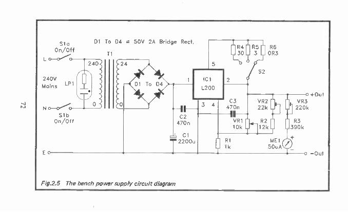
Sba On/Off
L
240V Mains LP1
No—o•-*"....* Sib
On/Off
E 0
D1 To 04 = 50V 2A Bridge Rect.
240
Ti
24
DI To 04
5
ICI
L200
3 4
C2 470n
Cl "'" 2200u
Fig.2.5 The bench power supply circuit diagram
T
R4 30
C3 470n
R5 3
S2
R6 OR3
IF-
VR2 22k
VR1 — R2 10k I -4-112k
R1 MEI 1 k 50uA
+Out VR3 220k
R3 390k
C Out
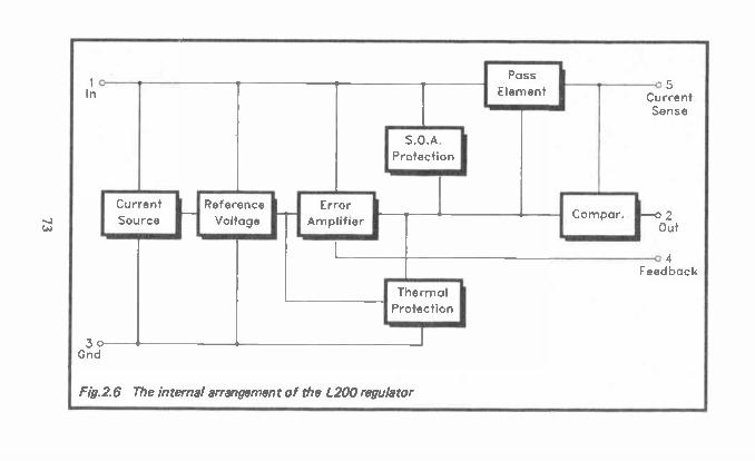
1 o In
3 o Gnd
Current
Source
Reference
Voltage Error
Amplifier
S.O.A.
Protection
Pass
Element
Fig.2.6 The internal arrangement of the L200 regulator
Cornpar.
o 5 Current Sense
•2 Out
Feedback
exceeds a certain threshold level (0.45 volts), the current limiting circuit comes into operation. This pulls the output of the error amplifier (and thus the output of the supply) lower in voltage. This prevents the output current from more than marginally exceeding the current limit threshold level. Even with a short circuit on the output, the output current will only slightly exceed the current limit threshold level, with the output voltage being pulled down to virtually zero. The other two stages are concerned with safe operating area and thermal overload protection. Safe area operation incidentally, means avoiding combinations of voltage and current that could damage the device.
Returning to the bench power supply circuit diagram, on the input side of ICI there is the usual mains isolation and step-down transformer (Ti), full wave bridge rectifier (D1 to D4), and a smoothing capacitor (Cl). The specified value for CI is the minimum I would recommend. If you can obtain a 3300µ or 4700µ component having a suitable voltage rating, then this should give a lower output "hum" level at hie out-put currents. C2 is needed to aid the stability of IC1 (as is C3 on the output side of the device).
The L200's internal reference voltage generator has a nominal potential of 2.77 volts (2.65 volts minimum — 2.85 volts maximum). The minimum output voltage of the supply is therefore no more than 2.85 volts. VR1 would enable the maximum output voltage to be set at over 30 volts if it was not for the inclusion of VR2 and R2. VR2 is adjusted to limit the maximum output voltage to 20 volts, or some other desired figure up to about 25 volts. As explained previously, the maximum output current can not be provided at voltages of more than about 20 volts, but it is useful to have voltages in the 20 to 25 volt range available even if less than the full current is available. It is possible that with VR2 at maximum resistance it will still not be possible to achieve an output quite as high as 25 volts. If this should happen, and you require output potentials right up to 25 volts, simply make R2 a little higher in value (say 18k). VR3, R3, and ME1 form a volt-meter at the output of the unit, making it easy to accurately set the desired output voltage using VR1. VR3 can be set for a full scale value of 20 or 25 volts.
74
S2 is used to switch one of three current sensing resistors into circuit. R4, R5 and R6 give approximate limit currents of 15 milliamps, 150 milliamps, and 1.5 amps respectively. You may like to use different limit currents for the two lower limit levels, or to add more limit currents. The correct value for a given limit current is obtained by dividing 0.45 by the required limit current. The limit current should be in amps, and this gives an answer in ohms (or use milliamps to obtain an answer in kilohms).
Construction Although the circuit of the bench power supply is quite simple, there are a number of awkward aspects when construc-ting the unit. Firstly, the unit is mains powered and the usual safety precautions should be observed.
IC1 has to dissipate quite a lot of power when the supply is operating with high output currents and low output voltages. It must therefore be mounted on a large heatsink. One having a rating of about 2 degrees Celsius per watt should suffice. What is probably a better alternative is to Ilse a fairly large case of all metal construction to house the project, and to then use this as the heatsink. ICI can be mounted direct onto a panel of the case or the chassis, but it will probably be more convenient to fit it on an "L" shaped bracket which is then bolted to the case at a convenient place: If you adopt this method the bracket must be quite large and made from a heavy gauge of aluminium (preferably 16 s.w.g.) so that it conducts heat into the case efficiently. There is no need to insulate the L200's heat-tab from the case since this tab connects internally to the "Ground" terminal, which will presumably connect to the earthed case anyway.
Several of the components require some explanation. With a maximum output current of 1.5 amps, the rating for Tl given in the components list (3 amps) might seem rather high. There is a problem with many variable voltage power supply designs in that the maximum permissible input voltage of the regulator is quite low, and the difference between the unload-ed and loaded input voltages can be quite substantial. The maximum continuous input potential for the L200 is 40 volts. Using a 24 or 25 volt mains transformer the unloaded input
75
voltage to the regulator will not be far short of this figure. In theory, multiplying the secondary voltage of the transformer by 1.41 gives the unloaded d.c. voltage, from which about 1 volt or so has to be deducted in order to take into account the voltage drops through the rectifier. In practice the actual voltage seems to be significantly higher than the figure derived from a calculation of this type. Multiplying by 1.5 or so and deducting nothing seems to give a more realistic figure.
The loaded d.c. voltage using a 24 or 25 volt transformer will be only about 24 or 25 volts. There are inevitably voltage drops through the series regulator circuit, and this permits a maximum output voltage with the full rated current at output voltages of about 20 volts and less. Using a mains transformer having a generous current rating helps to maximise perform-ance at high output voltages. The rating is not as generous as it might at first appear. When using a bridge rectifier the current rating of the transformer needs to be substantially higher than the maximum d.c. output current that will be required. I would therefore recommend that T 1 should not have a current rating of less than 3 amps. A higher rating is preferable, as the unit would then be able to supply the full 1.5 amp output current at output voltages of up to 25 volts. However, this would only marginally improve the usefulness of the unit, and higher current transformers would be very large, heavy, and quite expensive.
LP1 must be a panel neon of the type that has a built-in series resistor for operation on the 240 volt mains supply. R4 to R6 require values that are in the E24 series, but obtaining suitable components could be difficult. Not all component suppliers stock E24 series resistors of such low values. An easy solution to the problem is to make up each resistor from two or three resistors connected in series or parallel. As a couple of examples, R4 could consist of two 15 ohm resistors wired in series, or R6 could be made up from three 0.1 ohm resistors connected in series.
Ideally the output voltage would be monitored using a 20 or 25 volt panel meter. Panel meters of this type seem to be unavailable these days, making it necessary to use a current meter plus external series resistor in order to obtain a volt-meter action. The only real drawback of doing this is that the
76
meter's calibration will be inappropriate. There is no real difficulty in converting the 0 to 50 calibration of the meter into corresponding output voltages, especially if the meter is set up to read 0 to 25 volts. However, the unit will be easier to use and will look neater if the scale of the meter is recali-brated. This is not too difficult, and with most modern panel meters the front unclips and then removing two small screws enables the scale plate to be detached. The existing lettering can be carefully scraped away using a tool having a sharp point, and then rub-on transfers can be used to add a 0 to 20 or 0 to 25 scale. Alternatively, the existing lettering can be left in place, with a new scale being marked on paper and then fitted in place over the original.
This is all quite straightforward in theory, but in practice you must remember that panel meters are very delicate mechanisms that are easily damaged. If you decide to alter the existing scale or fit a new one over it, exercise great care when working on the meter. If you are not reasonably skilled at working with delicate mechanisms you would probably be well advised to simply use the original scale.
Setting Up Start with VR2 and VR3 at maximum resistance, and VR1 at minimum resistance. Using a multimeter to check the output voltage should produce a reading of around 2.65 to 2.85 volts. Adjust VR1 for an output of 20 volts, and then adjust VR3 for a reading of 20 volts on MEI. Next set VR2 at minimum resistance and VR1 at maximum resistance. Then set VR2 to produce the required maximum output voltage from the unit. The power supply is then ready for use.
Components for Bench Power Supply (Fig. 2.5)
Resistors (0.25 watt 5% unless noted) RI lk R2 12k R3 390k 1% R4 3OR R5 3R R6 0.3R 1 watt
77
Potentiometers VR I VR2 VR3
Capacitors Cl C2 C3
10k lin 22k miniature preset 220k miniature preset
2200µ 40V elect 470n polyester 470n polyester
Semiconductors ICI L200 DI —D4 50 volt 2A bridge rectifier
Miscellaneous SI S2 T1
ME1 LP1
Rotary mains switch 3 way 4 pole rotary (only one pole used) Standard mains primary, 24 or 25 volt 3 amp secondary winding 50µA moving coil panel meter Panel neon for 240 volt a.c. operation Large heatsink (see text)
Logic Pulser A logic pulser is the digital equivalent to a signal generator for linear circuits. The analogy is quite a loose one though, since a signal generator is used to supply a signal to a chain of amplifiers or other processing stages, and the progress of the signal through these stages is then traced using an oscilloscope or a signal tracer. With digital circuits it is unusual to have a series of signal processing stages. Probably the only common example of a digital processing chain is a series of divider stages. The crystal calibrator described earlier uses a circuit of this type, and they are to be found in a few other applica-tions such as baud rate generators for serial interfaces. With a circuit of this type a logic pulser can be used in a fashion that is similar to the way in which a signal generator is used with linear circuits.
Probably a more common use for a logic pulser is as a clock oscillator for a circuit that is under development, or when
78

testing faulty circuits. It is often used to provide a very low frequency clock signal (sometimes less than 1Hz) so that the action of a circuit is slowed right down to make it more easily analysed. This method is not applicable to all types of logic circuit, and it will often not work properly with complex microprocessor based circuits. Where it can be used, it offers what is often a very good means of tracking down the defect in faulty equipment, or a design fault in a new design that is not performing as expected.
As a simple example of how a logic pulser might be used in practice, we will return to the divider chain example mention-ed previously. One way of testing a circuit of this type is to disconnect the clock oscillator, inject the output from the logic pulser to the input of the divider chain, and then check the output signal from each divider stage using an oscilloscope. In practice this is an over involved method of testing the circuit, since the pulser is not really needed. You might just as well use the clock oscillator to provide the input signal to the divider chain!
Suppose that you do not have an oscilloscope though, but that you do have a logic probe. You can check with the logic probe that there is a pulsing output from each divider stage, and the probe might give you some idea of the mark-space ratio of the signal at each output. However, it will not give conclusive evidence that the signals are alright, and it may not show exactly what is wrong if a stage is faulty. Using a logic pulser to provide the input signal would enable a very low clock frequency to be used, and the output of the first divider stage would then operate at a rate which could easily be followed by looking at the "high" and "low" 1.e.d.s on the logic probe. The outputs of subsequent divider stages might operate at too low a frequency, with long waits being neces-sary in order to check that the correct divider action is being obtained. To overcome this problem the output frequency of the pulser could be increased. As you check further along the divider chain the clock frequency can be stepped up in order to maintain a suitable output frequency from the stage being tested.
Many logic circuits contain more complex signals than those from simple divider circuits, but with everything slowed
79

down to a suitable rate it is always going to be easier to check that suitable waveforms are present, and that the relative timing of signals are correct. Having two or three logic probes can be a definite advantage when undertaking this checking of comparative signal timing. It is also much easier to check the mark-space ratio of signals if they are at low frequencies. You can see from the on/off times of the logic probe's "high" and "low" 1.e.d.s whether or not the mark-space ratio is approximately correct. This method is not as good as having an oscilloscope or a high quality logic analyser, but it is a good substitute if available funds will not accommodate the purchase of one of these units.
Circuit Operation Ideally a logic pulser should cover a wide frequency range, with a large number of mark-space ratios available. Units of this type can be very complex, with the mark and space dura-tions separately adjustable over wide limits and having crystal controlled accuracy. For most purposes this sort of sophistica-tion is not required, and a more simple approach will suffice. This unit has the simple configuration shown in the block diagram of Figure 2.7.
The circuit is based on a little used form of oscillator known as a "ring" oscillator. Two negative edge triggered monostables are wired in series, and have the output of the second monostable coupled back to the input of the first one, completing the "ring" connection. Oscillation is achieved because as the output pulse from one monostable ends, it generates a negative edge that triggers the other monostable. The circuit therefore oscillates indefinitely, with first one monostable being triggered, and then the other.
Circuits of this type can be a bit unreliable, and in particu-lar, they can sometimes be a bit reluctant to start. This problem is avoided here because when the supply is first connected, the trigger inputs of both monostables will be taken to outputs that will be at logic O. This effectively provides a negative trigger signal that ensures the circuit starts to oscillate. It is possible that both monostables will trigger at switch-on. This will not matter, because the first output pulse to end will have no effect on the other monostable. It
80
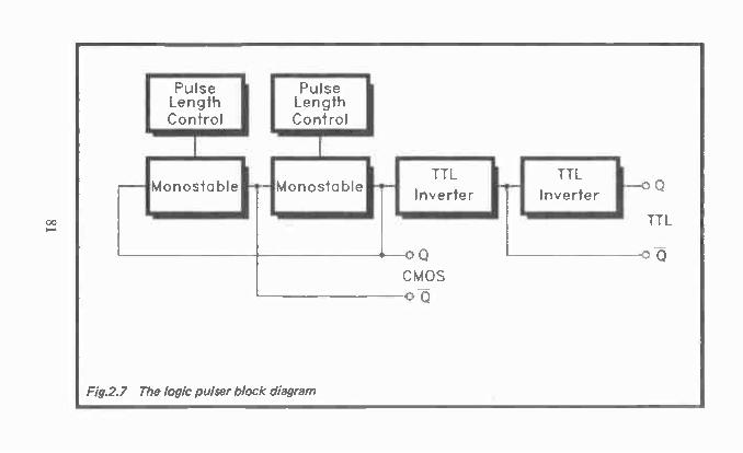
Fig.2.7 The logic pulser block diagram

will supply a negative edge to the other monostable, but it will have no effect as that monostable is already triggered. When the output pulse from the second monostable ceases, it triggers the first one, and oscillation then carries on normally. There have certainly been no problems with the prototype ever failing to start oscillating. Short circuits or overloads on outputs can result in an oscillator of this type stalling, but it is merely necessary to switch off, wait a second or so, and switch on again in order to restart the circuit.
An advantage of a ring oscillator in this application is that it enables the mark and space durations to be set using entirely separate timing circuits. In effect, one monostable sets the mark duration while the other sets the space time. This arrangement gives anti-phase outputs (Q and not Q), with one monostable providing the Q output and the other provid-ing the not Q signal. This enables the unit to be used in applications where a two phase clock signal is required. The circuit is based on two CMOS monostables, and it therefore provides (5 volt) CMOS compatible outputs. The Q signal is fed to two TTL inverters wired in series, and these provide TTL compatible Q and not Q output signals.
The Circuit The full circuit diagram for the logic pulser appears in Figure 2.8. ICI and IC2 are the monostables, and these are based on 4047BE astable/monostable multivibrators which are connec-ted here to act as negative edge triggered, non-retriggerable monostables. Each monostable has five switched timing capacitors, giving nominal output pulse durations of lObts, 10012s, lms, 10ms, and 100ms. Logic would seem to dictate that for the 101.is pulse duration a capacitor of 100p in value would be required, and not the 22p specified for Cl and C6. In fact the total timing capacitance is about 100p, but it is largely made up from the internal capacitance of the 4047BE integrated circuit.
Normally a 43k timing resistor is switched into circuit, but for both monostables there is the option of switching over to a 430k timing resistor. This has the effect of multiplying the pulse duration by a factor of ten, and is included to enable the maximum pulse duration of each monostable to be
82

00 te.1
o +5V
10
14 8
1. R1 R2
430k 43k
4 2
SI
ICI
4047BE
5 7 9 12
-
C11 7 100n OV
CI 2 22p_
7 -11r—C-2—' In
S2 C3
GA R__191 .C4 -
00n
\ C1 I us
10
-
i R3 R4
T. 43 t 0k 43k
L-6 F
à S3
14 8 4 2
IC2
40478E
5 7 9 12
IC3 = 74LS14
C6 m__22p_
• cs -
• FLI21_n,,
(\ do lu
IC3a
IC3b
o p
CMOS o -0
Fig.2.8 The circuit diagram for the logic pulser
o -0
TTL
o OV

increased to 1 second. The unit could be made more versatile by replacing each changeover switch and pair of resistors with a 39k fixed resistor and a 470k potentiometer wired in series. This would enable the pulse durations to be varied from lOps to is in five ranges. However, unless you have access to an oscilloscope so that the potentiometers could be fitted with calibrated dials, it is probably better to opt for the two switched resistors for each monostable.
The two TTL inverters are provided by IC3, which is a hex Schmitt Trigger/inverter. The other four inverters are left unused, and no connections are made to the relevant pins of IC3.
The unit requires a 5 volt supply and it has a current con-sumption of about 11 to 12 milliamps. It can be powered from a 9 volt battery using the same circuit that was suggested for the crystal calibrator (see Figure 2.3).
Construction of the unit is reasonably simple. S2 and S4 can be 12 way 1 pole rotary switches having an adjustable end-stop set for 5 way operation. The values of the four resistors are unusual ones, but they are available in the E24 series of values. ICI and IC2 are CMOS devices, and apparent-ly lack any form of static protection on one or two of their pins. They are not particularly expensive components, but in view of their greater than normal vulnerability to static charges it would be sensible to scrupulously observe the usual precautions.
Components for Logic Pulser (Fig. 2.8)
Resistors (all 0.6 watt 1% metal film) R1 430k R2 43k R3 430k R4 43k
Capacitors Cl 22p ceramic plate 2% C2 I n polyester 5% C3 lOn polyester 5% C4 100n polyester 5%
84

C5 1p polyester 5% C6 22p ceramic plate 2% C7 in polyester 5% C8 lOn polyester 5% C9 100n polyester 5% CIO 1p polyester 5% C11 100n ceramic
Semiconductors ICI 4047BE IC2 4047BE IC3 74LS14
Miscellaneous Si s.p.d.t. miniature toggle S2 5 way 1 pole rotary S3 s.p.d.t. miniature toggle S4 5 way 1 pole rotary
14 pin d.i.l. i.c. holder (3 off)
Dynamic Transistor Tester The transistor tester featured in Chapter 1 of this book, like most transistor testers, makes d.c. checks on the components under test. For most purposes this method of testing is perfectly satisfactory, but it is possible for a transistor to have good current gain but to still be less than fully operational. There is an interesting alternative form of transistor tester in the dynamic type. In other words, rather than making d.c. current gain checks, the device is tested using an a.c. input signal. This signal is usually at a frequency of several mega-hertz, where any deficiencies in the high frequency responses of test components will be revealed.
Figure 2.9 shows the arrangement used in this dynamic transistor checker. An r.f. oscillator generates the test signal, and this is followed by a buffer amplifier that ensures loading effects by the subsequent circuits do not cause the oscillator to stall. The device under test is placed in a simple amplifier circuit. It would be possible to switch the biasing, load resistors, etc. to suit n.p.n. or p.n.p. devices, but it is easier to simply have separate bias circuits and sockets for the two
85
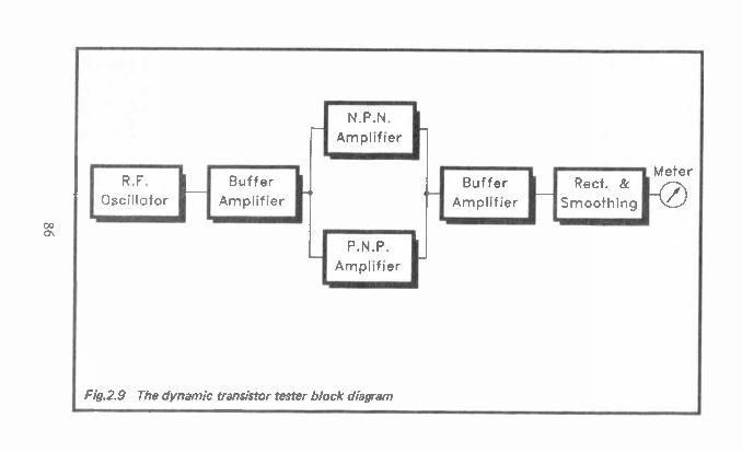
R.F.
Oscillator
Buffer
Amplifier
P.N.P.
Amplifier
Fig.2.9 The dynamic transistor tester block diagram
Buffer
Amplifier
Rect. ac
Smoothing
Meter

types of transistor. The amplified signal is fed to a buffer amplifier which feeds a simple rectifier and smoothing circuit. This provides a d.c. output voltage that is roughly propor-tional to the a.c. output voltage from the amplifier, which is in turn proportional to the a.c. gain of the test transistor. A meter registers the d.c. output voltage, and the reading on the meter therefore gives an indication of how well (or otherwise) the test component is functioning.
There is a slight difficulty with a unit of this type in that it must provide correct biasing for any test device. There is no way of knowing what current gain the test components are likely to have, and enormous variations are quite likely. Low gain devices might offer a current gain of only about ten times, while the highest gain components offer around one hundred times as much current gain. It is important that all test devices operate at the same collector current. Otherwise there is a likelihood of some transistors seeming to offer excellent a.c. gain simply because they have a high d.c. current gain and are operating at high collector currents. The opposite would occur with low gain devices, which would operate at low collector currents and would conse-quently have low a.c. gains at the frequencies involved here.
One solution would be to have manually adjustable biasing so that the d.c. test conditions could be accurately set up at the correct levels for each component. This would be a bit slow and cumbersome though, and there are bias circuits which can largely negate the effects of different d.c. current gains. The bias circuit of Figure 2.10 was popular in the early days of transistor amplifiers. In those days the variations in current gain from one component to another were not the only problem. The germanium transistors in use at that time had what were often quite large leakage currents. For modern silicon devices the leakage level is usually just a fraction of a microamp. For germanium devices a leakage level of a milli-amp or two would not be anything out of the ordinary. Variations in current gain plus wide variations in leakage level made it impossible to obtain accurate biasing using simple single resistor biasing, even if the type which utilizes negative feedback was used.
The bias circuit of Figure 2.10 guarantees accurate biasing
87

Fig.2.10 A bias circuit that guarantees accurate results with any transistor that is functioning properly
with any component that offers at least a moderate amount of current gain and which does not have a grossly excessive leak-age level. Suppose that the supply potential is 9 volts, and that a bias voltage of about 4.5 volts is therefore needed at the collector of TR1. R3 could be made about four times higher in value than R4, and the biasing of the circuit would then be set so that there was about 1 volt across R4. As the collector and emitter currents of a transistor are not radically different, this would give about 4 volts across R3, which would leave about 4 volts across the collector—emitter terminals of TR1.
This gives more or less the required biasing. On the face of it the bias level at the collector of TRI is a little high at 5 volts instead of 4.5 volts. However, the 1 volt across R4 reduces the maximum peak to peak output voltage swing of the circuit by 1 volt. Optimum biasing is therefore with the collector of TRI half way between +1 volt and +9 volts, or at 5 volts above the 0 volt rail in other words. C2 bypasses R4 so that it does not introduce a.c. negative feedback that would reduce the a.c. gain of the amplifier.
88
For this method of biasing to be successful it is essential to be able to set the emitter voltage of TRI at the correct level. This is not too difficult since the emitter voltage of a silicon transistor is about 0.6 volts less than base voltage. In our previous example where 1 volt was needed at the emitter of TR1, this would be achieved by using values for RI and R2 that would bias the base of TRI to 1.6 volts. The values of the bias resistors should be fairly low so that loading by TRI does not significantly pull the base voltage away from the required figure. This is not a major problem since the emitter resistor introduces a lot of d.c. negative feedback which boosts the input resistance of the transistor to a relatively high figure. This method of biasing is therefore largely independent of the transistor's current gain. It is the values of the resistors which have a more major effect on the exact bias voltages.
The Circuit The full circuit diagram for the dynamic transistor tester appears in Figure 2.11. The r.f. oscillator is a crystal type, and is much the same as the one used in the crystal calibrator unit described previosuly. I used a 12MHz crystal for Xl, but any type having a frequency of about 10 to 13MHz should be satisfactory (but avoid overtone types, as in this circuit these will operate at their fundamental and not the appropriate overtone). Use of a crystal might seem a bit extravagant, but these components are available quite cheaply these days, and using an inductor would probably not provide a significant reduction in the cost of the unit. Like the oscillator in the crystal calibrator, the usual capacitors from the collector and base of T RI to earth have been omitted. Stray circuit capacitances will almost certainly be sufficient to produce strong oscillation, but capacitors of about 6p8 can be added to the unit if necessary.
TR2 is the buffer stage, and is an emitter follower type. The output of the unit is likely to be slightly excessive, and so an attenuator is used as the emitter load resistor for TR2. This gives an output level that will produce a strong signal from any good quality test device, but clipping is unlikely to occur. C2 couples the output of TR2 to the amplifier in which the test device is connected. Sla connects the signal
89

‘C,
TR1,2,3 = 13C549 D1,2 = 0A91
Cl R2 R5 r R7 100n 1 k 22k L 680
X1 TR2 12MHz
— 1°H. R RI 3
330k 680
•-1 1—*
C2 10n
N Sla
TR 1 ft R4 R6 6 100 k8
B
f R9 6k8
R11 220
NPN E B •
PNP
R8 fl ••••1C3: R10 220 00n 22k
E
1C4 T 100n S2
On/Off
N
P î
Sib VR1 C5 100k
C: 12 I 81 TR3 4_147in
R12 R13 D1 ME1 680 680 50uA
E31
9V
C6 100n
Fig.2.11 The dynamic transistor tester circuit diagram
through to the n.p.n. or the p.n.p. test amplifier, as required. Sib connects the output from the selected circuit through to the emitter follower buffer stage based on TR3. C5 couples the output from this stage to a conventional rectifier and smoothing circuit. This directly drives the meter circuit which has VR1 as the preset sensitivity control.
The component layout of the unit is not particularly critical, but avoid any long wires or obvious feedback routes which could adversely affect results. I used a good quality panel meter for ME1, but as readings are relative and the scaling is arbitrary, a low cost "level" or "tuning" meter should be perfectly satisfactory. These usually have lower sensitivities than the specified full scale current of 50µA, but it should still be possible to set the sensitivity of the unity at a suitable level by adjusting VR1. I would not recommend using a meter having a full scale current of more than 250 microamps, but most low cost meters seem to be 200µA or 250µA types.
The current consumption of the circuit is about 20 mili-amps. If it is only likely to receive intermittent use a "high power" PP3 size battery is adequate as the power source. If the unit is likely to receive a great deal of use it would be better to opt for a higher capacity 9 volt battery, such as a PP9 type or six HP7 cells in a plastic holder.
The only adjustment needed to the completed unit is to set VR1 for a suitable sensitivity. This can only be given a final setting in the light of experience after the unit has been in use for a while. The optimum setting is one which does not allow any overloading of the meter on high gain compon-ents, but which gives something very close to full scale deflection of the meter when testing devices of this type.
Results using a unit of this type are quite interesting. Transistors of the same general type tend to give virtually identical readings, even though their d.c. current gains might be radically different. Devices which have high transition frequencies but relatively low d.c. current gains will usually give reasonably high readings when tested with this unit. At the frequency involved in this test it is more the gain/band-width product of test components that determine their level of performance, rather than their d.c. current gains. The unit
91

will soon sort out any components which offer good d.c. current gains but which are faulty and offer poor a.c. gain.
Components for Dynamic Transistor Tester (Fig.2.11)
Resistors (all 0.25 watt 5%) RI R2 R3 R4 R5 R6 R7 R8 R9 R10 R11 R12 R13
Potentiometer VRI
Capacitors C 1 C2 C3 C4 C5 C6
Semiconductors TR1 TR2 TR3 D1 D2
Miscellaneous SI
330k 1 k 680R 100R 22k 6k8 680R 220R 6k8 22k 220R 680R 680R
100k miniature preset
100n ceramic lOn polyester 100n ceramic 100n ceramic 47n polyester 100n polyester
BC549 BC549 BC549 0A91 0A91
d.p.d.t. miniature toggle
92
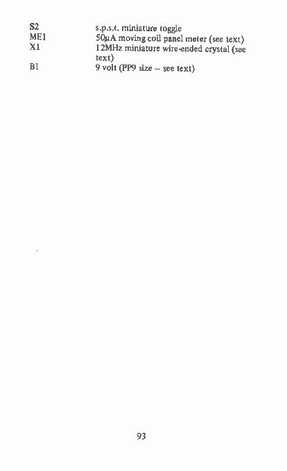
S2 s.p.s.t. miniature toggle ME! 50µA moving coil panel meter (see text) X1 12MHz miniature wire-ended crystal (see
text) B1 9 volt (PP9 size — see text)
93

u4741C CA3140E LF351N LF441CN TLC555CP
1 (-«-Me- 38 E 3 E
4( 35
1N4002 1N4148 0491
74121 74LS14 74LS90 4047BE
4017BE
Fol.-14
8 (
LM35DZ
V+ Out V—
NC
BC549 78L05 BC559 78L12
E • Out 16 Corn
In
9
8069
L200
1 3 5 2 4
Fig.2.12 Semiconductor leadout and pinout details. I.C.s are shown as top views — transistors as base views (see also Figs 1.4 and 1.5)

Notes
95

Notes
96

Notes
97

Notes
98

Notes
99