monolithic diode arrays for quasioptical millimeter …
TRANSCRIPT

FINAL REPORT
MONOLITHIC DIODE ARRAYS FOR QUASIOPTICAL MILLIMETER WAVE
BEAM STEERING
Advanced Research Projects Agency (ARPA) Defense Small Business Innovation Research Program
ARPA ORDER No. 5916, Arndt
Issued by U.S. Army Missile Command under Contract #DAAH01-94-C-R263
Period Covered: 01 January 1995 thru 31 March 1995
Prepared by:
Millitech Corporation So. Deerfield Research Park So. Deerfield, MA 01373-0109 (413) 665-8551
Principal Investigator: Ellen L. Moore and Debabani Choudhury Senior Engineer
The views and conclusions contained in this document are those of the author and should not be interpreted as representing the official policies, either expressed or implied, of the Advanced Research Projects Agency or the U.S. Government.
Li Tlxia iocuaeat has beefc approved to public leleass and sola its oatntoitipTtt ia uoliinitecl /\ millitech

REPORT DOCUMENTATION PAGE Form Approved OMB No. 0704-0188
Puolic reoorting Du/den for tnn collection of information n «imiw to wcnqe I hour oer resoome. including tfte time for reviewing imtructionv searcmng e».«ing data sourc«. gathering and ma.ntain.ng the data needed, and completing and re.«mng me collecoon of information. Send comment» regarding th« burden estimateor any,other aueetofth» collection of information/Including suggestion» »or reducing dm buroen. to Washmgton Headouarten Servwes. Oirectoratejor ,n*^»«^^,'°"L*od IV^nini >*""*>" Oavn Highway Suite 1204 Arlington. VA 22202-O02. and to the Office of Management and Budget. EaperworX Redu«ionrYO|e«(070A-0188). Washington. PC 20503.
1. AGENCY USE ONLY (leave blank) 2. REPORT OATE
28APR95 3. REPORT TYPE AND DATES COVERED
Final Report 9/22/94 - 3/31/95_
4. TITLE AND SU8TITLE Monolithic Diode Arrays for Quasioptical Millimeter Wave Beam Steering
6. AUTHOR(S)
Ellen L. Moore Debabani Choudhury
7. PERFORMING ORGANIZATION NAME(S) AND ADORES5<ES) Millitech Corporation South Deerfield Research Park South Deerfield, MA 01373
9. SPONSORING/MONITORING AGENCY NAME(S) AND ADDRESSES)
U.S. Army Missile Command Redstone,Arsenal, AL 35898-5248
5. FUNDING NUMBERS
DAAH01-94-C-R263
I. PERFORMING ORGANIZATION REPORT NUMBER
A5017
10. SPONSORING /MONITORING AGENCY REPORT NUMBER
11. SUPPLEMENTARY NOTES
12a. DISTRIBUTION /AVAILABILITY STATEMENT
Approved for public release; distribution unlimited
12b. DISTRIBUTION CODE
13. ABSTRACT (Maximum 200 words)
This final report presents the details of the research and design effort for the first phase of a prograrr to produce a monolithic diode array for quasioptical beam steering at millimeter wavelengths. Beam steering is accomplished by adding a linear phase shift across the aperture of an antenna. The quasioptical circui performing this task comprises a 2-dimensional square metallic mesh on gallium arsenide loaded with Schottk; varactor diodes. The mesh is an inductive element and the diodes have a variable capacitance which i controlled by the bias voltage. The phase of a wave transmitted through the monolithic array is changed b. an amount determined by the diode capacitance. In this design the beam steering array is a 115 mm diamete mosaic of 12.7 mm x 12.7 mm dies. The array is controlled by a 6 layer drive circuit, which can arbitrarily bias each individual die. The circuit is computer controlled to step the beam in a 4 x 4 point raster pattern After Phase 2 is completed the beam steering array will be incorporated into existing imaging systems t< achieve super-resolution.
During Phase 1 we designed the Schottky varactor diodes, mesh circuit, 115 mm beam steering array and the drive circuit to bias the array. In the final report we show the design of these devices and the DC tes t results on the diodes.
14. SUBJECT TERMS 15. NUMBER OF PAGES
33 16. PRICE COOE
17. SECURITY CLASSIFICATION OF REPORT
Unclassified
18. SECURITY CLASSIFICATION OF THIS PAGE
Unclassified
19. SECURITY CLASSIFICATION OF ABSTRACT
Unclassified
20. LIMITATION OF ABSTRACT
UL Standard Form 298 (Rev. 2-89) •menoed by ANSI Std. 239-1« »»•102
NSN 7540-01-280-S500

ABSTRACT
This final report presents the details of the research and design effort for the first phase of a program to produce a monolithic diode array for quasioptical beam steering at millimeter wavelengths. Beam steering is accomplished by adding a linear phase shift across the aperture of an antenna. The quasioptical circuit performing this task comprises a 2- dimensional square metallic mesh on gallium arsenide loaded with Schottky varactor diodes. The mesh is an inductive element and the diodes have a variable capacitance which is controlled by the bias voltage. The phase of a wave transmitted through the monolithic array is changed by an amount determined by the diode capacitance. In this design the beam steering array is a 115 mm diameter mosaic of 12.7 mm x 12.7 mm dies. The array is controlled by a 6 layer drive circuit, which can arbitrarily bias each individual die. The circuit is computer controlled to step the beam in a 4 x 4 point raster pattern. After Phase 2 is completed the beam steering array will be incorporated into existing imaging systems to achieve super-resolution.
During Phase 1 we designed the Schottky varactor diodes, the mesh circuit, the 115 mm beam steering array, and the drive circuit to bias the array. In the final report we show the design of these devices and the DC test results on the diodes.
Accesion For
NTIS CRA&I DTIC TAB Unannounced Justification
D D
By Distribution /
Availability Codes
Dist
/H
Avail and / or Special

1.0 INTRODUCTION
This final report presents the details of the research and design effort for the first phase of a program to produce a monolithic diode array for quasioptical beam steering at millimeter wavelengths. During Phase 1 we developed the design for Schottky varactor diodes and incorporated this device design into the design of an optical mesh phase shifting array. We have processed 12.7x12.7 mm dies on GaAs and have completed DC measurements on the diodes in these samples. In this report we present the diode design and dc test results, the drive circuit design, the phase shifting array design, the status of the specially designed RF test set up, and an outline of how the work will be continued into Phase 2.
Electronic beam steering is accomplished by adding a linear phase shift across the aperture of an antenna. The optical principle is based on a simple diffraction model as shown in Fig.l [Goldsmith, 1989], where d = 27iA.dx sine. In this Figure dx can be the spacing between feed elements in a traditional phased array or it can represent the spacing between active elements in a monolithic array. For small angles the total phase shift across an aperture having diameter D is A<|>= 2rcD0A,. TO scan the antenna beam by an angle 0 requires a phase shift every distance dx equal to 2%/X times 6.
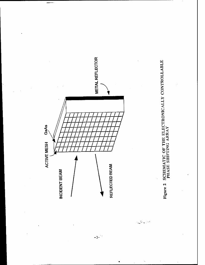
The quasioptical circuit comprises a 2-dimensional square metallic mesh on gallium arsenide loaded with Schottky varactor diodes. The mesh is an inductive element and the diodes have a variable capacitance which is controlled by the bias voltage. The phase of a wave transmitted through the monolithic array is changed by an amount determined by the diode capacitance. To simplify the problem we designed an array which reflects instead of transmits, thereby requiring only 1/2 the amount of phase shift on each pass. Fig.2 shows the schematic of the electronically controllable phase shifting array [1]. This design also simplifies the biasing of the array.
The proposed beam steering array layout is shown in Fig.3. The array has a 115 mm diameter with a square hole in the center for the focal plane antenna elements. The 12.7 mm squares show the location of the individual die. Each die is biased separately by a six layer driVe circuit described in Section 3.0, thus giving the desired phase shift across the aperture of the antenna. All diodes on a given die are biased the same.
- 1 -

WAVELENGTH >.
DIRECTION OF PROPAGATION
REFERENCE DIRECTION
Figure 1 LINEAR PHASE GRADIENT FROM BEAM SCANNING
-2-
e o HI u. Ill
////////////// //////////////
to / ////////////// < 1 «\ // ///////////// o\// /////////////
' 1 1 1 1 1 1 1 1 1 1 1 1 I to III III 1 II UJ
E^ i \ > 1 \ 1- T \ Ü < / \ i s / \ s
S \ 2 cu / \ Ö I- / \ *7 z / \ P. ULI / \ ^ Q / 1 ^ O / ^ UJ z I ^ a:
o H Z o u ><
u 1—I
z o es H
HO
OH
<l f=C/2
VI
u 3 OH
-3-

2 3 4 1)\
6 /' "7 8 9 10 11 12 13s \14
A 16 17 18 19 20 21 22 '28
24 25 26 27 28 29 \
30 31 32
38
33 34 35
\36 37 39 40 41/
42 \ 43 T"T 45 46 47 48 49 £T> \
51 \2 53 54 55 56 57 5y /
59
-Si. 62 J33. .^
,/
Figure 3 BEAM STEERING ARRAY LAYOUT
-4-

Upon completion of Phase 2 our immediate application of this beam steering array will be to achieve super-resolution in a compact imaging camera.
2,0 MONOT JTHIC VARACTOR DIODE PHASE SHIFTING ARRAY
The idea of using the diode grids for electronic beam steering was introduced by Lam et al. [1]. As shown in Fig.2, when an incident beam reflects off the diode grid, the direction of the reflected wave can be controlled by progressively varying the reflection phase across the grid. The reflection phase of the diode grid can be controlled by varying the DC bias on the diodes. We plan to develop a monolithic Schottky varactor diode phase shifter on GaAs substrate. For this we have to address two design issues — device design as well as the embedding circuit design.
2.0.1. DEVICE DESIGN — SCHOTTKY VARACTOR DIODE
The critical element of our monolithic phase-shifting array is the planar Schottky diode. One aim of this work is to design a Schottky varactor diode which demonstrates maximum possible capacitance variation with bias voltage.
All varactors depend on a nonlinear capacitance-voltage and some type of barrier to real current flow. The most common is the reverse biased Schottky varactor diode. This diode consists of a Schottky contact on top of a doped semiconductor with a back ohmic contact. Fig.4 shows the schematic diagram of a circular anode Schottky varactor diode. The metal- semiconductor junction forms a barrier to electron flow while the semiconductor depletion region forms a capacitor with the well known inverse-square-root voltage dependence.
The three most important circuit parameter of a varactor are the breakdown voltage, zero bias capacitance and the series resistance. They affect the level of impedance the varactor will present, the amount of power the varactor will handle and the amount of power the varactor will dissipate in a circuit. A higher phase range can be achieved for a single grid by increasing the capacitance ratio of the device. Our goal is to design an epitaxial profile that will provide a suitable capacitance-voltage
-5-

t a: CM
1
ÜJ
i CO ffl D 05 0)
ts CD
O
u in
Q O Z < es
U g U <
o
<:
a« HO
E« G«
u 3 6X1
-6-

characteristics with a minimum series resistance and higher breakdown voltage.
a) DEVICE PHYSICS AND CTRCUIT MODEL
The circuit model of a varactor diode is shown in the Fig.5, where Cj is
the voltage variable capacitance of the depletion region, Rj is the junction
resistance of the depletion region and Rs is the series resistance of the diode. The modulation of the junction capacitance with bias voltage is used for the phase variation.
The gallium arsenide (GaAs) is chosen rather than other semiconductors because of its high mobility, easy isolation and good Schottky contact. At 94 GHz, the absorption loss for a Cr-doped 20 mils thick GaAs is negligible (about 0.013 dB, calculated from data in [2]).
The structure used in this study has a hyperabrupt doping profile, i.e. the net doping concentration of the epitaxy decreases with the distance from the metal-semiconductor interface. For the same voltage variation, the capacitance of a hyperabrupt junction changes more than that of a comparable abrupt junction device. This should result in an improved beam steering array because phase shift depends upon the nonlinearity of the capacitance-voltage law.
The doping concentration is given by
Nd(x) = x0 + N0exp(-x/L) (1)
where N0 is the impurity atom concentration at the surface, x0 is the zero bias depletion width and L is the characteristice length of the exponential decay. The design method is based on Lundien et al.'s [3] design algorithm of an exponentially retrogated doping profile. In the depletion approximation, the one dimensional Poisson equation,
dfydx2 = -qNd/ss (2)
is integrated where (|> is the electric potential, q is the electronic charge, and ss is the dielectric permittivity of the semiconductor. The boundary conditions are <Kx=0)=0 and f(x=Wdep)=(|>j - Vapp, where fy is the junction potential, Wdep is the depletion width of the space charge region, and V is the applied voltage. This leads to an algebraic relation, Vapp - F(Wdep), which is used to compute the corresponding CV relation
C = ssA/Wdep (3)
-7-

ü
tt
tf)
D O
O H U <
< >
Es. o Esü D O
*^
U
u «n
3
-8-

where A is the area of the varactor. For the circular anode as shown in Fig.4, the junction capacitance is given by
Cj = (esAAV) + (36sA)/(2R0)
where R<, is the anode radius [4].
(4)
The junction resistance, Rj represents the conduction current through the Schottky barrier, and is a parasitic element for the varactor operation. This effect is minimized by confining the applied voltage values between the point at which forward current becomes significant, i.e., between the device turn-on and the reverse breakdown limit.
The low frequency series resistance of the device is due to the resistance of the undepleted region, the substrate and the ohmic contact.
R-s ~~ Repi + ^sub + Ro ihm (5)
The largest component of the series resistance is due to the undepleted epitaxial layer, which is calculated from,
Lepi
Repi =1 dx/(qunNdA) (6) W dep
where fxn is the electron mobility and Tepi is the epitaxial thickness. An empirical expression for the electron mobility is used
m = (104)/(l+V(Nd/(1017))) (7)
1 9-1 where Nd is in units of cm" and |j.n is in units of cm (Vs)" [5]. The substrate series resistance is
R3Ub=l/(4R0asub) (8)
where asub is the substrate conductivity and R0 is the anode radius. The substrate is usually highly doped to minimize the substrate resistance. The ohmic contact resistance is given by,
R-oc_ Rsc'A oc >(9)
-9-

where Aoc is the ohmic contact area and RsC is the ohmic contact specific resistance.
The voltage applied to a Schottky diode operating in the varactor mode is generally bounded by the diode turn-on voltage in the forward direction and by voltage breakdown in reverse direction. Neglecting the tunneling, the reverse breakdown is caused by avalanche multiplication [6]. Depending on the device design, reverse breakdown can occur while the depletion edge is still in the active layer, or it can occur after the depletion edge has crossed the active/buffer layer interface, or 'punched- through'. Avalanche breakdown is the result of a multiplicative effect involving the creation of electron-hole pairs. An electron which gains sufficient energy from the electric field across the depletion region can, upon collision with an atom, break a lattice bond and create an electron- hole pair. If the electron-hole pair is sufficiently excited by the electric field, it can in turn create additional electron-hole pairs. The voltage at which this process becomes a chain reaction, is the breakdown voltage. To obtain the maximum capacitance variation and to reduce the diode series resistance, the active layer thickness is chosen so that punch-through occurs at the same time the critical field is reached.
The breakdown voltage is computed as the applied voltage at which the ionization integral becomes unity,
W, epi
1= I Aexp[-{b/E(x)}2]dx=l (10)
where E(x) is the electric field in V/cm, A = 3.5 x 10⁵ /cm and b = 6.85 x 10⁵ V/cm [7]. The electric field is obtained from the one dimensional Poisson's equation. The boundary conditions are imposed. The field is set to zero at x = Wepi.
Fig.6 shows the semiconductor layer structure for the hyperabrupt junction varactor. The epilayer thickness is 0.61 micron. Since MBE machines typically require manual adjustment of the doping level, a 'staircase' approximation has been used in implementing the hyperabrupt profile. The n+ layer thickness is 1.4 micron with a doping concentration of5xl018cm"3.
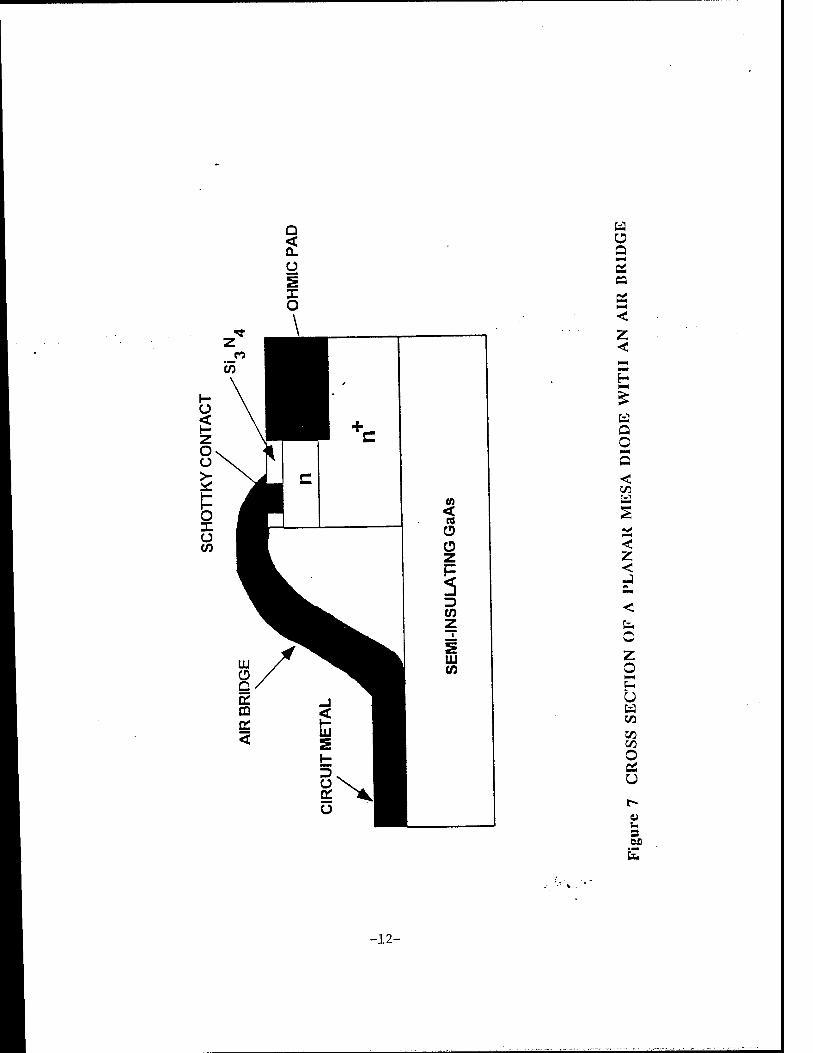
Fig.7 depicts a schematic of a planar mesa diode with air bridge. The parasitic components of this structure are shown in Fig.8. In the. figure, Cp
is the parasitic pad-to-pad capacitance, Cf is the capacitance between the
anode contact finger and the n/n+ GaAs, Ls is the air bridge inductance, Rs
-10-

Hl O < U. DC D C/3 UJ I
2 O er: IX. X
Q. Ill G
Cd mm
H fc- O Cd X
E- U
es H C/2jV
<l t< °t «1 8* ca. I* Sa «■«
0) u 3 Ml
N0UVH1N30N00 ONldOQ
-ii-
Q < Q.
Ü
Ed Ü Q /^ a
< z < mm
i-
Q O
<
< Z < ■MM
<
o z o U
in CO O eel u
u b. 3
-12-

o
HI—
LAAAH
a: CO
O
0)
O
Ed Q O
< in Ed
H fa O WD u
C/3 <
fa
3 U
U
Z Ed J < >
a Ed
00
0) u s 6H
fa
-13-

is the diode series resistane, Rj and Cj are the junction resistances and capacitances respectively.
2.0.2 monrc GRID PHASE SHIFTER DESIGN
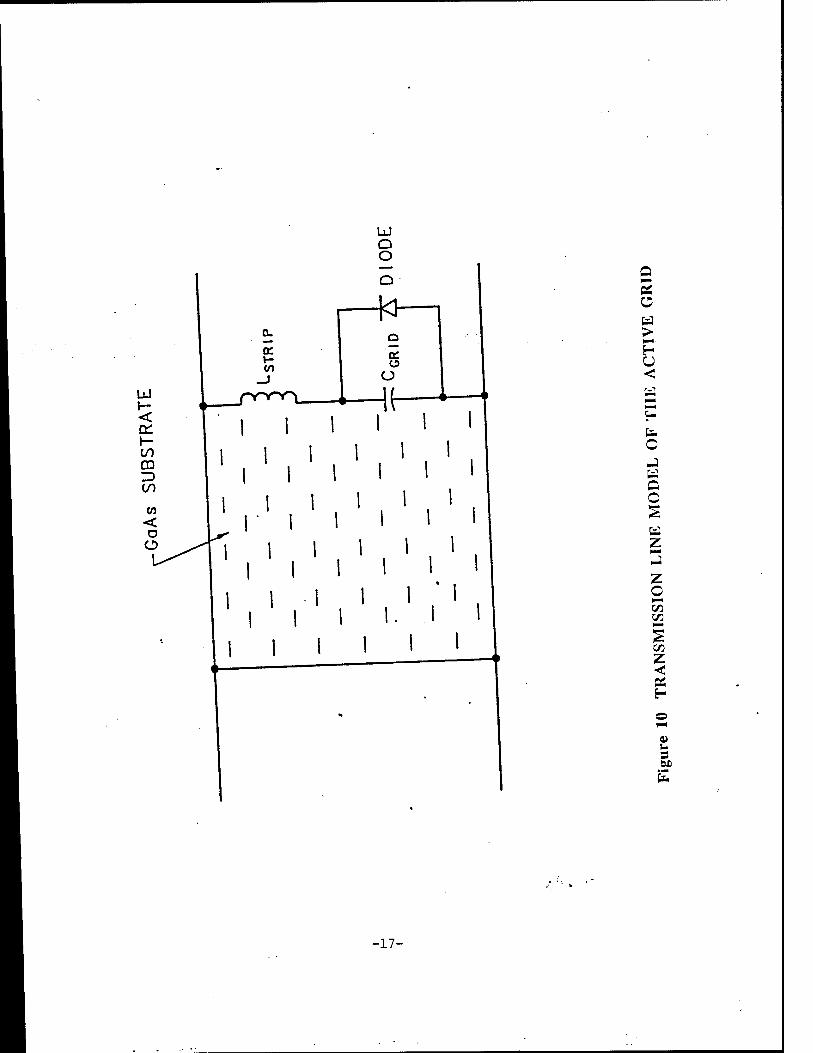
The diode grid phase shifter is a square or rectangular mesh of metal strips on GaAs substrate. Fig.9 shows the periodic grid structure loaded with Schottky vatactor diodes. The horizontal strips are used as bias lines. Changing reactance with bias controls the phase of the reflected wave. Design considerations include grid period, dielectric constant and angle of incidence. The design approach is based on transmission line theory and equivalent circuit model.This approach has been taken because it is relatively easy to incorporate both the diode model and supporting substrate into the analysis.
The transmission line model of the phase shifter grid periodically loaded with varactor diodes is shown in Fig. 10. Each diode defines a unit cell of the grid. The grid needs to be optimized for incident signals at the design frequency by optimizing the dimensions and metal patterns of the unit cell and electrical properties of the grid substrate. Each diode in the array is presented with an embedding impedance which is a function of the grid structure repeated throughout each unit cell.
At the RF frequencies, quasi-optical reflection type diode grid phase shifter can be modelled as a two port network. The port 1 is the front of the grid itself, and the second port is the location in the grid unit cell where the diode is mounted. Obtaining the scattering parameters of an arbitrary quasi-optical grid phase shifter is a challenging problem. To date, solutions for arbitrary shaped unit cell metal patterns are still not available. However, significant progress has been made for specific metal patterns such as strips for grids assumed to be infinite in extent. Solutions make use of grid symmetry to reduce the problem of analyzing the entire grid to the simpler analysis of an equivalent waveguide unit cell. The equivalent waveguide then can be solved using techniques developed for the analysis of structures placed inside waveguides, or by the use of numerical three-dimensional finite element electromagnetic solvers. Solutions of this type, because they assume grids of infinite extent, completely ignore grid edge effects. Nevertheless, they have been found to provide reasonably good accuracy. ■:. ^ . -
Let us assume an infinite grid with a uniform plane wave normally incident upon the grid surface. Symmetry then allows us to replace the
-14-
walls of the unit cell in the grid with electric and magnetic walls to form an equivalent waveguide unit cell. For the vertical electric field polarization, this waveguide has magnetic walls on the sides and electric walls on the top and bottom. The walls extend in the +z and -z directions, with the diodes in the z = 0 plane. In effect this reduces the problem of analyzing the grid to that of analyzing an equivalent waveguide with electric and magnetic walls. The propagating mode is TEM, and the evanescent modes couple to the currents in the unit cell metal pattern.
It is desirable to keep the grid unit cell as small as possible to avoid the generation of undesirable substrate modes. If A,d is the wavelength in the dielectric, then for unit cells larger than Xd, substrate modes will begin to propagate. It should be reasonable to build grids as large as 0.8 Xd. For 94 GHz, this places the upper bound for the unit cell as 710 urn.
Hewlett Packard's High Frequency Structure Simulator (HFSS) has been used to extract the embedding impedance of the complex geometry of the unit cell. To start with, a unit cell size of 400 um x 400 urn with a vertical strip width of 20 (am is used to design the grid for 94 GHz. Diode metal dimensions are included in the gap at the center of the strip. Fig. 11 and 12 show the schematic of an unit cell and its simple equivalent circuit. Layouts of the HFSS waveguide cells used to simulate the grid design is shown in Fig. 13. The de-embedded S-parameters are normalized to 377 Q, the free space impedance. Computed S-parameters of the structure have been used to model the equivalent inductance and capacitance of the unit cell.
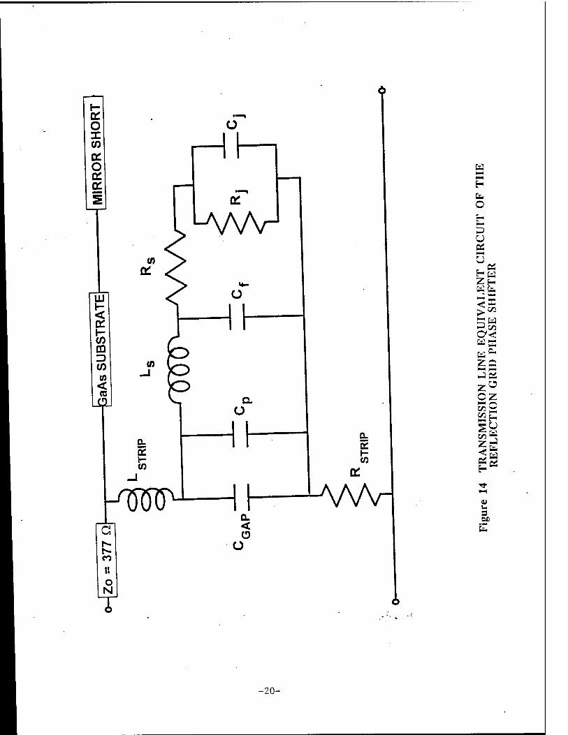
A simple transmission line model of the reflection grid phase shifter is shown in Fig. 14. Free space is represented as a transmission line with a characteristic impedance of 377 Q. The GaAs substrate appears as a section of the line with an impedance of 105 Q. The substrate is backed by a metal short which serves as a reflector. In our first design we have not used any matching dielectric substrate on the front of the wafer. This will introduce impedance mismatch at the air/GaAs diode interface.
The above structure has been simulated using Touchstone to evaluate the phase range. The simulation is carried out for different junction capacitance values which varies with the DC bias voltage. The phase of the reflected wave and the reflection loss is calculated. Fig. 15 shows the Cmax/Cmin versus phase shift plot calculated for Cmax = 30 fF. A maximum reflection loss of about -3 dB is calculated. Fig. 16 shows the bias voltage versus phase shift plot for the same device.
-15-

-16-
H O
U C/3
Q Ed Q < O J Ed a H U
£ VD ^"Cd ^O QO
o<
s ox
es ü Ed >
U <
Es. o Ed Q O
Ed Z
z o *"<
>—
Z <
u 3 BJ3
-17-
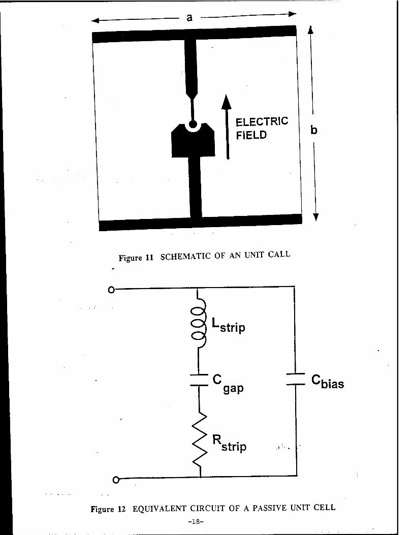
Figure 11 SCHEMATIC OF AN UNIT CALL
*-strip
gap
strip
bias
o—
Figure 12 EQUIVALENT CIRCUIT OF A PASSIVE UNIT CELL
-18-

<
J Cä U
ta Q
u Ed >
Es.
S H Es. O H
O
■-a
9) u 3
-19-
O X CO
O
HI
co CD
CO (A < re
Lai
o
Wvv (0
(0
CL a: C0
-w G
II
f
CL a: i-
£
AAAr
Ed
O
3 U es
Cd Es. d-
£s ~Cd
a«: CdE Cd0- ZQ
zü
oz £2 EH
Z^
u 3 (M)
-20-

IT) CM
IÖ
es o fa H O j
—'
\
-HiV"." ""■ ■■■"'
■
fa *^
to
fa
< *-* El
;
1-
T—
2.25
3
3
.75
Cna
ax/C
min
CO
GO CS fa >
s
u X es
u Q fafa E-5-" <©
1- < E
I ._ !— ■
lO _ — ■
__ o o
« u 3 OX)
fa
L. i
O
CM
o o o g O W 0 :
(saayoaa) uiHS-BSVHd
-21-

CM i
HI O <
I
I
CO <
CÜ
in i
CO
o CD
© CM 00 CO
o o CN
O
i/3
1/3
63©
o g < 5
^63 sau
I—I
63 63 HQ
%%
U1*
0) u 3 6X1
(S33y03Q) UIHS 3SVHd
-22-

DIODE
Figure 17 SCHEMATIC OF THE DIE SPA
-23-

DIODE
Figure 18 SCHEMATIC OF THE DIE DPA
-24-

We have proposed two different monolithic diode grid die designs. Fig. 17 shows the schematic of the dies with diodes in only one direction (SPA). Fig. 18 shows the concept of the monolithic dies with diodes in two perpendicular directions (DPA).
2.0.3 MONOLITHIC DIODE ARRAY FABRICATION AND DC RESULTS
The fabrication of the monolithic varactor diode phase shifting arrays have been carried out in the Semiconductor Device Laboratory of Millitech. To begin the process, ohmic patterns are defined followed by Schottky metallization contacts. Mesas are then etched and subsequently circuit metal is defined. The wafer is then passivated by a dielectric. Dielectric windows are then opened to span plating contact metal.
Fig. 19(a) and (b) show the photographs of the processed SPA and DPA dies respectively. Fig.20 shows the photograph of the device portion of the fabricated monolithic array.
Fig.21 shows the measured CV characteristic of a varactor diode with 5.4 urn diameter. The ratio of the capacitance at zero bias to the capacitance at breakdown is about 4.9. The typical measured breakdown voltage is about -12V.
3.0 DRIVE CIRCUIT
The circuit which will bias the full 115 mm diameter array of diodes was a task in the statement of work, however we supported the design with Millitech IR&D because of limited Phase 1 funds. Without such a circuit all of the diodes would be dc biased simultaneously with the result that there would be no phase gradient across the array. The circuit can arbitrarily bias each individual die and is controlled by a computer, which will scan the beam in a 4 x 4 point raster pattern. The 6 layers of this circuit are on both sides of 3 pieces of fiberglass. The first iteration of the photomasks for each layer are shown in Figure 22.
-25-

Figure 19(a) PHOTOGRAPH OF THE PROCESSED MONOLITHIC SPA DIE
Figure 19(b) PHOTOGRAPH OF THE PROCESSED MONOLITHIC DPA DIE -26-

Figure 20 CLOSE-UP OF THE DEVICE PORTION OF THE MONOLITHIC ARRAY
-27-

(0 .e o
C>4
CO i
■<fr ■
in ■
to ■
Lil O <
CO <
00 I
I
es c 5- U «< BS
>
< es es < z < Cs. ^ C £
2 ,1 es
u
< S = 5
es Cd
Cd
■ u Q Ed es
< Cd
Cd Q O z
Cd u 1—1
Cd G
<u u 3
(dj) aoNViiovdvo -28-

Fisure 22 FIRST ITERATION OF THE PHOTOMASKS FOR EACH LAYER OF THE DRIVE CIRCUIT _29_

4.0 RF TEST SET TIP STATUS
The phase shift test set-up described in the quarterly progress report is expected to be complete by mid-May. The only outstanding circuit components are the two subharmonic mixers, and the quasioptical components and fixtures will be completed by May 10. We are getting quotations for a near field range to measure the complete phase shifting array beam patterns during Phase 2.
5,0 PHASE 2 PLANS
Phase 2 will contain the tasks listed below.
1. All RF measurements 2. Beam steering pattern prediction 3. Modifications to the die based on DC and RF test results. We
expect three iterations including the design described in this report.
4. Build and test a small array of dies, 2x2 or 3x3. This will indicate the ease of manufacturing and assembling. An array larger than 12.7x12.7 mm2 die will be easier to test on the quasioptical set-up and give a larger aperture array for better RF results.
5. Build the 6-layer drive circuit for the 115 mm diameter beam steering array.
6. Build the 115 mm beam steering array. 7. Test the beam steering array on the near field range.
Some of these tasks will exceed the $375,000 limit and will be included in an addendum of the Phase 2 proposal.
6J SUMMARY AND CONCLUSIONS
The results of the phase 1 effort include Schottky varactor diode design, quasioptical mesh circuit design, development of 12.7 mm dies incorporating these designs and DC testing of varactor diodes. The measured CV and IV characteristics of the diodes are close to the design values. We have also designed a 115 mm diameter monolithic beam steering array and drive circuit, which will be manufactured and tested during Phase 2. The quasioptical phase shifting set-up is almost complete and we expect to begin RF tests on the 12.7 mm dies by mid-May. During phase 2, we will upgrade our RF test set-up to include a small near field
-30-

range to measure the beam steering capability of the 115 mm monolithic array.
ACKNOWLEDGMENTS
We would specially like to thank John Nicholson, who fabricated and DC tested the monolithic diode arrays and John Williams for the help in purchasing the GaAs wafers. We also would like to thank Sudarsanam Bandla and Richard Huguenin for many valuable technical discussions, encouragement and support.
REFERENCES
[1] Lam et al., "MM-wave diode grid phase shifters', IEEE Trans, on Microwave Theory and Tech., vol.36, no.5, pp.902-907, May 1988.
[2] M.N.Afsar, 'Dielectric measurements of millimeter-wave materials', IEEE MTT-32, no. 12, Dec. 1984.
[3] Lundien et al. 'Hyperabrupt junction varactor diodes for millimeter wavelength harmonic generators', IEEE MTT-31,1983.
[4] Rizzi, 'Planar varactor diodes for millimeter and submillimeter wavelengths', Ph.D. thesis, University of Virginia, 1994.
[5] Müller and Kamins, Device electronics for integrated circuits, John Wiley and Sons, NY, 1977.
[6] Sze, 'Physics of semiconductor devices', John Wiley and Sons, pp.99-106, 1981.
[7] Hilsum,' Simple empirical relationship between mobility and carrier concentration', Electronics Letters, vol.10, 1974.
[8] Goldsmith,P.F., 'Millimeter Wave Electronic Beam Scanning', Final Report, Air Force Contract # F29601-89-C-0047, 1989.
-31-