monolithic 3d inc. patents pending 1 monolithic 3d-ic re-inventing wafer scale integration the...
TRANSCRIPT

MonolithIC 3D Inc. Patents Pending 1
Monolithic 3D-IC
Re-Inventing Wafer Scale Integration
The Cubic IC System ~ 100X Advantage

3D Brain vs. 2D IC (1:3,000)
Jack Sun, vice president of R&D and chief technology officer at TSMC, said “to solve challenges associated with power constraint, the chip industry must "get some inspiration from the amazing human brain.”
Sun said “the human brain has about 100 billion neural cells, equivalent to about 1 trillion IC transistors, yet draws only about 20 watts of power. By contrast, an advanced IC with 3 billion logic cells draws about 200 watts of power,”
Panel debates keeping up with 'Gene's Law' Dylan McGrath
2/21/2011 10:01 PM EST

Monolithic 3D to Enable Redundancy/Repair
“Wafer” scale integration(Folded in 3D for Shorter Interconnect)
Ultra High complexity with Ultra High Yield,
Leveraging 3D Repair/Redundancy+ Transient Error Detection and Isolation
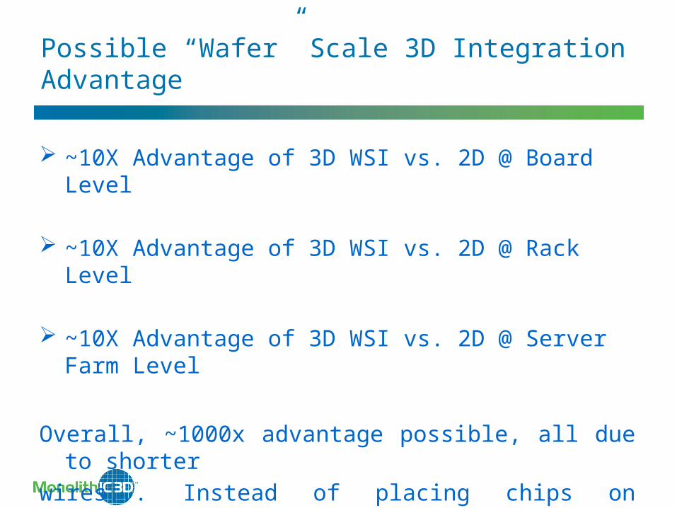
Possible “Wafer” Scale 3D Integration Advantage
~10X Advantage of 3D WSI vs. 2D @ Board Level
~10X Advantage of 3D WSI vs. 2D @ Rack Level
~10X Advantage of 3D WSI vs. 2D @ Server Farm Level
Overall, ~1000x advantage possible, all due to shorter
wires... Instead of placing chips on different packages,
boards and racks, we integrate on the same stacked chip

Cost of Defect
Charles Chiang, Jami KawaDesign for Manufacturability and Yield for Nano-Scale CMOSISBN 978-1-4020-5188-3

Repair
Monolithic 3D wafer where: All primary output are also wired to top layer All F/F input are switchable to be fed from top layer
Full test in the fab – preferably contact less Reconstruction of any failed logic-cone at the top
layer by Direct Write eBeam Switch F/F input to be fed from the top layer


Redundancy
Monolithic 3D wafer where: Each layer is overlaid with identical layer All primary output are exchangeable with the upper
layer All F/F input are switchable to be fed from upper layer
Self test In the fab – preferably contact less In the field
Replace any failed section with the one overlaid it.

A Novel Redundancy Scheme for Logic, Analog, …
Swap at logic cone granularity.
Redundant logic cone/block directly above, so no performance
penalty.
Negligible design effort, since redundant layer is exact copy.

Redundancy

Transient Error Detector
Use the redundancy to detect transient error Transient error could caused enormous problem –
“Toyota run- away” and could not be detected by current BIST
Compare the output of the two corresponding F/F and latch the error
