monoblock type pol, 12a dc-dc converter series · fpga/cpu’s, datacom/telecom systems,...
TRANSCRIPT

MYMGK1R812 SeriesMonoBlock type POL, 12A DC-DC Converter Series
MYMGK1R812 Series A03 Page 1 of 22
http://www.murata.com/products/power Export Control Code : X0863 Document No : DC_R190009
(Typical topology is shown. Murata recommends an external input fuse.)
PRODUCT OVERVIEW
The MYMGK1R812 series are miniature Mono Block type non-isolated Point-of-Load (PoL) DC-DC power converters for embedded applications. The tiny form factor measures only 10.5 x 9.0 x 5.6 mm. Applications include powering FPGA/CPU’s, datacom/telecom systems, Distributed Bus Architectures (DBA), programmable logic and mixed voltage systems.The converters have input voltage ranges of 4.5 to 8.0V or 8.0 to 15.0V and a maximum output current of 12A. Based on a fixed frequency synchronous buck converter switching topology, this high power conversion efficient PoL module features programmable output voltage 0.7 to 1.8V, On/Off control and Power Good signal output.These converters also include under voltage lock out (UVLO), output short circuit protection and over-current protection.
FEATURES■Settable output voltage from
0.7 to 1.8V■Up to 12A of output current■Quick response to load change ■Ultra small surface mount package
10.5 x 9.0 x 5.6mm■High efficiency of 93.5% max.■Outstanding thermal derating performance■Over current protection■On/Off control (Positive logic)■Power Good signal■High Reliability / Heat Shock Testing
700cycle (-40 to +125degC)■Meets CISPR 22 class B conducted emission
Typical unit
MYMGK1R812FRSRCin:47uF/10V x 2pcs (4.5≤Vin≤5.5V)
or 22uF/25V x 2pcs (5.5<Vin≤8.0V)Co:220uF/4V x 3pcs
MYMGK1R812ERSRCin:22uF/25V x 2pcsCo:220uF/4V x 3pcs
MYMGK1R812 SeriesSIMPLIFIED APPLICATION
Vin Vin
GND
ON/OFF
Vout
Trim
Power Good
Sense
Vout
CoCin

MYMGK1R812 SeriesMonoBlock type POL, 12A DC-DC Converter Series
MYMGK1R812 Series A03 Page 2 of 22
PERFORMANCE SPECIFICATIONS SUMMARY AND ORDERING GUIDE (Including series products)
PART NUMBER STRUCTURE
http://www.murata.com/products/power
Yes(Positive) 10.5 x 9.0 x 5.6
MY MGK 1R8 12 E
MYMGK1R812ERSRD 0.7-1.8(typ:1.8V)
12 21.6 0.8 ±1.5 ±1.0 12 8-15
R S DR
0.7-1.8(typ:1.8V)
12 21.6 0.8 Yes(Positive) 10.5 x 9.0 x 5.6
MYMGK1R812FRSRD 0.7-1.8(typ:1.8V)
12 21.6 0.8 ±3.0 ±1.0 5 4.5-8.0 100 4.7 92.0 Yes(Positive) 10.5 x 9.0 x 5.6
MYMGK1R812ERSR
50 2.0 90.4
1R812FRS1R812ERS
PART NUMBEROUTPUT INPUT
Efficiency(%)
100 4.7 92.0
ON/OFFPACKAGE
Vout(V)
Iout(A,max.)
Power(W)
R/N typ.(% of Vout)
Regulation(max.) Vin typ.(V)
Range(V)
Iin no load(mA)
Iin full load(A) (mm)
Line(%) Load(%)
MYMGK1R812FRSR ±3.0 ±1.0 50.7-1.8(typ:1.8V)
12 21.6 0.8 4.5-8.0 Yes(Positive) 10.5 x 9.0 x 5.6
±1.5 ±1.0 12 8-15 50 2.0 90.4
Part Number Product CodeMYMGK1R812FRSRMYMGK1R812ERSR
MYMGK1R812FRSRDMYMGK1R812ERSRD
1R812FRS1R812ERS
C
1.All specifications are at typical line voltage, Vout = 1.8V and full load, +25degC unless otherwise noted. Output capacitors are 220uF x 3 ceramic. Input capacitors are 22 uF x 2 or 47uF x 2 ceramic and plenty electrolytic capacitors. See detailed specifications. Input and Output capacitors are necessary for our test equipment.2.Use adequate ground plane and copper thickness adjacent to the converter.
Product MarkingBecause of the small size of these products, the product marking contains a character-reduced code to indicate the model number and manufacturing date code. Not all items on the marking are always used. Please note that the marking differs from the product photograph. Here is the layout of the Marking.
Codes(reference)
1Pin Marking1R812FRS Product code(Please see product code table beside)
□ Internal Manufacturing code
MC
Layout(reference)
1R812FRSM
Output Voltage Range1R8:(0.7-1.8Vdc)
Series Name
Maximum Output Current in Amps
Recommended Input Voltage RangeE:8-15VF:4.5-8V
ON/OFF Control LogicS:Positive Logic
Internal CodeInternal Code
Packaging CodeBlank:Standard Quantity
Murata products

MYMGK1R812 SeriesMonoBlock type POL, 12A DC-DC Converter Series
MYMGK1R812 Series A03 Page 3 of 22
COMMON SPECIFICATIONS
Thermal Protection/Shutdown (Recovery)
FUNCTIONAL SPECIFICATIONS OF MYMGK1R812FRSR (Note 1)
Vout 0.7 2.0
Full Load ConditionsLow LineNo Load CurrentShut-Down Mode Input Current
ON State RangeOFF State RangeControl Current
Power-Good Output (Pulled up to 5.0Vreg(typ.) internally)PGood TRUE (HI)PGood FALSE (LO)
http://www.murata.com/products/power
Measured in module (Note9,14) 135Thermal Protection/Shutdown Measured in module (Note9,14) 145 degC
2.5Thermal Resistance(Reference data) ψj-c Vin=12V, Vout=1.8V,Iout=12A (Note 15) 2.0 degC/WVin=12V, Vout=1.8V,Iout=6A (Note 15)
Moisture Sensitivity Level 3degC
grams10.5(typ.) x 9.0(typ.) x 5.6(max.)
ENVIRONMENTAL(Common) Conditions Minimum Typical Maximum UnitsOperating Ambient Temperature Range With Derating (Note 2,7) -40 85 degCStorage Temperature Range Vin = Zero (no power) -40 125 degC
MECHANICAL(Common) Conditions Minimum Typical Maximum UnitsMechanical Dimension L x W x H mmWeight 1.65
ON = +1.8Vmin. to +Vin-1.5Vmax. or left open 1.8 Vin-1.5 VOFF =-0.3V to +0.6Vmax. -0.3 0.6 V
Open collector/drain - mA
(Voset x 95%) < Vout < (Voset x 113%) VOut of above range V
FUNCTIONS Conditions Minimum Typical Maximum UnitsRemote On/Off Control (Note 4)Logic
DYNAMIC CHARACTERISTICS Conditions Minimum Typical Maximum UnitsFixed Switching Frequency 500 kHz
Dynamic Load Peak Deviation 50-100% load step, Note16 ±3.0% Voset
Startup Time (Vin ON) Vout = 1.8V (Vout = 5% to 95% of Vout) 1.4 msStartup Time (Remote ON) Vout = 1.8V (Vout = 5% to 95% of Vout) 1.4 ms
mA
Calculated MTBF (Note 3) +40degC, Vin = 5.0V, Vout = 1.8V, Iout = 50% 8x10⁶ hours
GENERAL and SAFETY Conditions Minimum Typical Maximum Units
EfficiencyVin = 5.0V, Vout = 1.8V, Iout = 12A 92
%Vin = 5.0V, Vout = 1.0V, Iout = 12A 90.2
Input Voltage -0.3 9.6
Source ONLYON/OFF Pin Power on, referred to -Vin -0.3 Vin-1.5
Input CurrentVin = 5.0V, Vout = 1.8V, Iout = 12A 4.7 A
VA
degC
Maximum Units
Start-up Threshold
125
Power on, referred to -Vin
ABSOLUTE MAXIMUM RATINGS Conditions Minimum Typical
Absolute maximums are stress ratings. Exposure of devices to greater than any of these conditions may adversely affect long-term reliability. Proper operation underconditions other than those listed in the Performance/Functional Specifications Table is not implied or recommended.
INPUT Conditions Minimum Typical
UnitsVV
PGOOD/Trim Pins
Rising input voltage 4.3 V
Maximum
Output Current Current-limited, no damage, short-circuit protected 0 12Storage Temperature Range Vin = Zero (no power) -40
Vin = 4.5V, Vout = 1.8V, Iout = 12A 5.2 A
Operating Voltage Range 4.5 5 8 V
Under Voltage Shutdown Note 12 4.1 VInternal Filter Type Capacitive
Iout = 0A, unit = ON 100 mA1

MYMGK1R812 SeriesMonoBlock type POL, 12A DC-DC Converter Series
MYMGK1R812 Series A03 Page 4 of 22
FUNCTIONAL SPECIFICATIONS OF MYMGK1R812FRSR (Note 1)
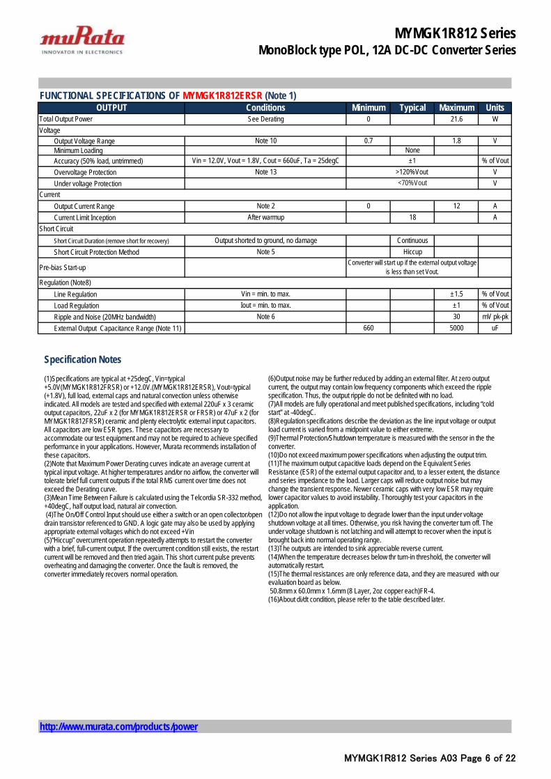
Output Voltage RangeMinimum LoadingAccuracy (50% load, untrimmed)Over Voltage ProtectionUnder Voltage Protection
Output Current RangeCurrent Limit Inception
Short Circuit Duration (remove short for recovery)
Short Circuit Protection Method
Pre-bias Start-up
Line RegulationLoad RegulationRipple and Noise (20MHz bandwidth)External Output Capacitance Range (Note 11)
http://www.murata.com/products/power
660 5000 uF
Vin = min. to max. ±3 % of Vout
Note 6 30 mV pk-pk
Converter will start up if the external output voltageis less than set Vout.
Note 2 0 12 AAfter warmup 18 A
Short Circuit
Regulation (Note8)
Output shorted to ground, no damage ContinuousNote 5 Hiccup
NoneVin = 5.0V, Vout = 1.8V, Cout = 660uF, Ta = 25degC ±1 % of Vout
Note 13 >120%Vout V<70%Vout V
Current
Total Output Power Range See Derating 0 21.6 WVoltage
Note 10 0.7 1.8 V
OUTPUT Conditions Minimum Typical Maximum Units
Iout = min. to max. ±1 % of Vout
MYMGK1R812 SeriesMonoBlock type POL, 12A DC-DC Converter Series
MYMGK1R812 Series A03 Page 5 of 22
FUNCTIONAL SPECIFICATIONS OF MYMGK1R812ERSR (Note 1)
Vout 0.7 2.0
Full Load ConditionsLow LineNo Load CurrentShut-Down Mode Input Current
ON State RangeOFF State RangeControl Current
Power-Good Output (Pulled up to 5.0Vreg(typ.) internally)PGood TRUE (HI)PGood FALSE (LO)
http://www.murata.com/products/power
Minimum Typical
V
Start-up Threshold Rising input voltage
ABSOLUTE MAXIMUM RATINGSInput Voltage -0.3 16
UnitsMaximumTypicalMinimumConditionsV
ON/OFF Pin Power on, referred to -Vin -0.3 6.3 V
Output Current Current-limited, no damage, short-circuit protected 0 12 A
PGOOD/Trim Pins Power on, referred to -Vin Source ONLY
Under Voltage Shutdown Note 12 4.1 V4.3 V
Storage Temperature Range Vin = Zero (no power) -40 125 degCAbsolute maximums are stress ratings. Exposure of devices to greater than any of these conditions may adversely affect long-term reliability. Proper operation underconditions other than those listed in the Performance/Functional Specifications Table is not implied or recommended.
Operating Voltage Range 8 12 15 VINPUT Conditions Minimum Typical Maximum Units
AInput Current
Iout = 0A, unit = ON 50 mAVin = 8.0V, Vout = 1.8V, Iout = 12A 3.0 AVin = 12.0V, Vout = 1.8V, Iout = 12A
Internal Filter Type Capacitive
2.0
mAConditionsGENERAL and SAFETY
Vin = 12.0V, Vout = 1.0V, Iout = 12A 85.2Vin = 12.0V, Vout = 1.8V, Iout = 12A 90.4
Efficiency %
Minimum1
Typical Maximum Units
-0.3
Units
OFF =-0.3V to +0.6V.max.
+40degC, Vin = 12.0V, Vo = 1.8V, Iout = 50% 8x10⁶ hours
Vout = 1.8V (Vout = 5% to 95% of Vout) 1.4 ms
Conditions
Vout = 1.8V (Vout = 5% to 95% of Vout) 1.4 ms500
±3.0% VosetConditions
Remote On/Off Control (Note 4)Minimum Typical Maximum
kHzMaximum Units
Startup Time (Remote ON)
DYNAMIC CHARACTERISTICS
Startup Time (Vin ON)Fixed Switching Frequency
Calculated MTBF (Note 3)
0.66.3ON = +1.8Vmin. to +6.3V max. or left open 1.8
LogicV
FUNCTIONSDynamic Load Peak Deviation 50-100% load step, Note16
VOpen collector/drain - mA
(Voset x 95%) < Vout < (Voset x 113%)Out of above range
MYMGK1R812 SeriesMonoBlock type POL, 12A DC-DC Converter Series
MYMGK1R812 Series A03 Page 6 of 22
FUNCTIONAL SPECIFICATIONS OF MYMGK1R812ERSR (Note 1)
Output Voltage RangeMinimum LoadingAccuracy (50% load, untrimmed)Overvoltage ProtectionUnder voltage Protection
Output Current RangeCurrent Limit Inception
Short Circuit Duration (remove short for recovery)
Short Circuit Protection Method
Pre-bias Start-up
Line RegulationLoad RegulationRipple and Noise (20MHz bandwidth)External Output Capacitance Range (Note 11)
http://www.murata.com/products/power
Converter will start up if the external output voltageis less than set Vout.
±1.5
Note 2 0 12Current
660
Short Circuit
Note 5 HiccupOutput shorted to ground, no damage Continuous
AAfter warmup 18 A
<70%Vout V
% of Vout
Conditions
Vin = 12.0V, Vout = 1.8V, Cout = 660uF, Ta = 25degC ±1 % of Vout
OUTPUTTotal Output Power See Derating 0 21.6 WVoltage
Minimum Typical Maximum Units
Regulation (Note8)
Note 13 >120%Vout V
Note 10 0.7 1.8 VNone
Iout = min. to max. ±1 % of Vout
5000 uFNote 6 30 mV pk-pk
Vin = min. to max.
(1)Specifications are typical at +25degC, Vin=typical +5.0V(MYMGK1R812FRSR) or +12.0V.(MYMGK1R812ERSR), Vout=typical (+1.8V), full load, external caps and natural convection unless otherwise indicated. All models are tested and specified with external 220uF x 3 ceramic output capacitors, 22uF x 2 (for MYMGK1R812ERSR or FRSR) or 47uF x 2 (for MYMGK1R812FRSR) ceramic and plenty electrolytic external input capacitors. All capacitors are low ESR types. These capacitors are necessary to accommodate our test equipment and may not be required to achieve specified performance in your applications. However, Murata recommends installation of these capacitors.(2)Note that Maximum Power Derating curves indicate an average current at typical input voltage. At higher temperatures and/or no airflow, the converter will tolerate brief full current outputs if the total RMS current over time does not exceed the Derating curve.(3)Mean Time Between Failure is calculated using the Telcordia SR-332 method, +40degC, half output load, natural air convection.(4)The On/Off Control Input should use either a switch or an open collector/open drain transistor referenced to GND. A logic gate may also be used by applying appropriate external voltages which do not exceed +Vin(5)“Hiccup” overcurrent operation repeatedly attempts to restart the converter with a brief, full-current output. If the overcurrent condition still exists, the restart current will be removed and then tried again. This short current pulse prevents overheating and damaging the converter. Once the fault is removed, the converter immediately recovers normal operation.
(6)Output noise may be further reduced by adding an external filter. At zero output current, the output may contain low frequency components which exceed the ripple specification. Thus, the output ripple do not be definited with no load.(7)All models are fully operational and meet published specifications, including “cold start” at -40degC.(8)Regulation specifications describe the deviation as the line input voltage or output load current is varied from a midpoint value to either extreme.(9)Thermal Protection/Shutdown temperature is measured with the sensor in the the converter.(10)Do not exceed maximum power specifications when adjusting the output trim.(11)The maximum output capacitive loads depend on the Equivalent Series Resistance (ESR) of the external output capacitor and, to a lesser extent, the distance and series impedance to the load. Larger caps will reduce output noise but may change the transient response. Newer ceramic caps with very low ESR may require lower capacitor values to avoid instability. Thoroughly test your capacitors in the application. (12)Do not allow the input voltage to degrade lower than the input under voltage shutdown voltage at all times. Otherwise, you risk having the converter turn off. The under voltage shutdown is not latching and will attempt to recover when the input is brought back into normal operating range.(13)The outputs are intended to sink appreciable reverse current.(14)When the temperature decreases below thr turn-in threshold, the converter will automatically restart.(15)The thermal resistances are only reference data, and they are measured with our evaluation board as below.50.8mm x 60.0mm x 1.6mm (8 Layer, 2oz copper each)FR-4.(16)About di/dt condition, please refer to the table described later.
Specification Notes

MYMGK1R812 SeriesMonoBlock type POL, 12A DC-DC Converter Series
MYMGK1R812 Series A03 Page 7 of 22
Internal Circuit Diagrams
ON/OFF internal circuit diagram and using guide
Power Good(P.G) internal circuit diagram and using guide
http://www.murata.com/products/power
Vin
To ON/OFF terminalof control IC
GND
ON/OFF
Pull UP ResistanceMYMGK1R812FRSR :12kohm(±0.5%)MYMGK1R812ERSR :100kohm(±0.5%)
Pull DOWN ResistanceMYMGK1R812FRSR :10kohm(±0.5%)MYMGK1R812ERSR :33kohm(±0.5%)
Recommended application
P.GLogic Control
Circuit
100kohm(±5%)
Vin
P.G
Regulator
Vout:5V(±10%) Vin>5.2V(without Tolerance)
Source Current0.025mA min.
Sink Current1mA max.
P.G Pull-down FET
Connect to other converter's ON/OFF terminal etc.

MYMGK1R812 SeriesMonoBlock type POL, 12A DC-DC Converter Series
MYMGK1R812 Series A03 Page 8 of 22
http://www.murata.com/products/power
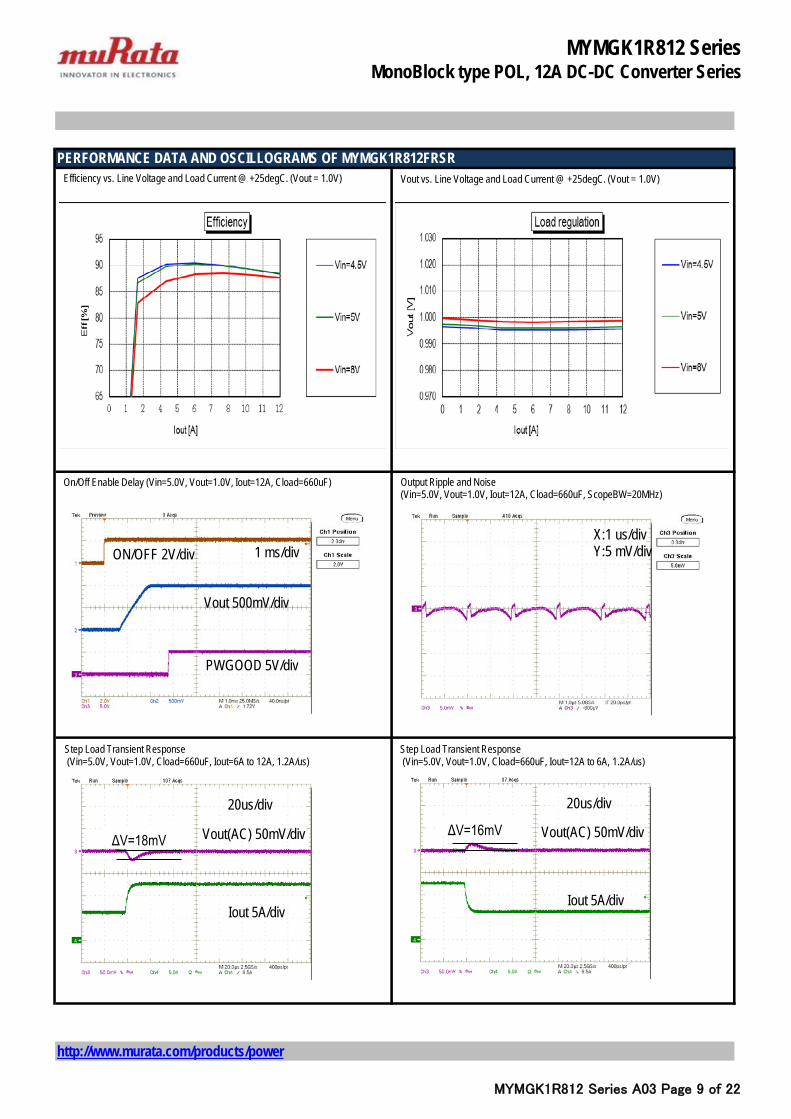
PERFORMANCE DATA AND OSCILLOGRAMS OF MYMGK1R812FRSR
Step Load Transient Response(Vin=5.0V, Vout=0.7V, Cload=660uF, Iout=6A to 12A, 1.2A/us)
Step Load Transient Response(Vin=5.0V, Vout=0.7V, Cload=660uF, Iout=12A to 6A, 1.2A/us)
On/Off Enable Delay (Vin=5.0V, Vout=0.7V, Iout=12A, Cload=660uF) Output Ripple and Noise (Vin=5.0V, Vout=0.7V, Iout=12A, Cload=660uF, ScopeBW=20MHz)
Efficiency vs. Line Voltage and Load Current @ +25degC. (Vout = 0.7V) Vout vs. Line Voltage and Load Current @ +25degC. (Vout = 0.7V)
ΔV=18mVΔV=16mV
PWGOOD 5V/div
Vout 200mV/div
1 ms/divON/OFF 2V/divX:1 us/divY:5 mV/div
20us/div
Vout(AC) 50mV/div
Iout 5A/div
20us/div
Vout(AC) 50mV/div
Iout 5A/div
MYMGK1R812 SeriesMonoBlock type POL, 12A DC-DC Converter Series
MYMGK1R812 Series A03 Page 9 of 22
http://www.murata.com/products/power
PERFORMANCE DATA AND OSCILLOGRAMS OF MYMGK1R812FRSR
Step Load Transient Response(Vin=5.0V, Vout=1.0V, Cload=660uF, Iout=6A to 12A, 1.2A/us)
Step Load Transient Response(Vin=5.0V, Vout=1.0V, Cload=660uF, Iout=12A to 6A, 1.2A/us)
On/Off Enable Delay (Vin=5.0V, Vout=1.0V, Iout=12A, Cload=660uF) Output Ripple and Noise (Vin=5.0V, Vout=1.0V, Iout=12A, Cload=660uF, ScopeBW=20MHz)
Efficiency vs. Line Voltage and Load Current @ +25degC. (Vout = 1.0V) Vout vs. Line Voltage and Load Current @ +25degC. (Vout = 1.0V)
ΔV=16mVΔV=18mV
PWGOOD 5V/div
Vout 500mV/div
1 ms/divON/OFF 2V/divX:1 us/divY:5 mV/div
20us/div
Vout(AC) 50mV/div
Iout 5A/div
20us/div
Vout(AC) 50mV/div
Iout 5A/div
MYMGK1R812 SeriesMonoBlock type POL, 12A DC-DC Converter Series
MYMGK1R812 Series A03 Page 10 of 22
http://www.murata.com/products/power
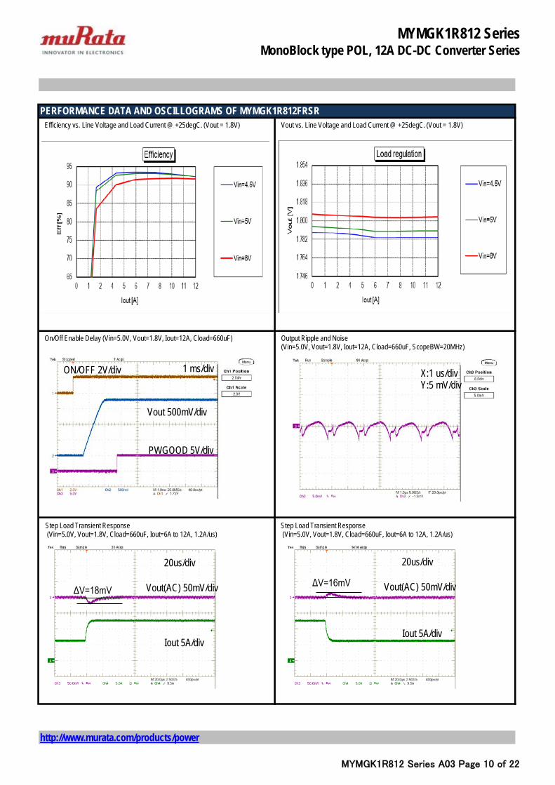
PERFORMANCE DATA AND OSCILLOGRAMS OF MYMGK1R812FRSR
Step Load Transient Response(Vin=5.0V, Vout=1.8V, Cload=660uF, Iout=6A to 12A, 1.2A/us)
Step Load Transient Response(Vin=5.0V, Vout=1.8V, Cload=660uF, Iout=6A to 12A, 1.2A/us)
On/Off Enable Delay (Vin=5.0V, Vout=1.8V, Iout=12A, Cload=660uF) Output Ripple and Noise (Vin=5.0V, Vout=1.8V, Iout=12A, Cload=660uF, ScopeBW=20MHz)
Efficiency vs. Line Voltage and Load Current @ +25degC. (Vout = 1.8V) Vout vs. Line Voltage and Load Current @ +25degC. (Vout = 1.8V)
ΔV=16mVΔV=18mV
PWGOOD 5V/div
Vout 500mV/div
1 ms/divON/OFF 2V/div X:1 us/divY:5 mV/div
20us/div
Vout(AC) 50mV/div
Iout 5A/div
20us/div
Vout(AC) 50mV/div
Iout 5A/div

MYMGK1R812 SeriesMonoBlock type POL, 12A DC-DC Converter Series
MYMGK1R812 Series A03 Page 11 of 22
http://www.murata.com/products/power
PERFORMANCE DATA AND OSCILLOGRAMS OF MYMGK1R812ERSR
Step Load Transient Response(Vin=12.0V, Vout=0.7V, Cload=660uF, Iout=6A to 12A, 1.2A/us)
Step Load Transient Response(Vin=12.0V, Vout=0.7V, Cload=660uF, Iout=12A to 6A, 1.2A/us)
On/Off Enable Delay (Vin=12V, Vout=0.7V, Iout=12A, Cload=660uF) Output Ripple and Noise (Vin=12V, Vout=0.7V, Iout=12A, Cload=660uF, ScopeBW=20MHz)
Efficiency vs. Line Voltage and Load Current @ +25degC. (Vout = 0.7V) Vout vs. Line Voltage and Load Current @ +25degC. (Vout = 0.7V)
ΔV=21mVΔV=20mV
PWGOOD 5V/div
Vout 200mV/div
1 ms/divON/OFF 2V/divX:1 us/divY:2 mV/div
20us/div
Vout(AC) 50mV/div
Iout 5A/div
20us/div
Vout(AC) 50mV/div
Iout 5A/div

MYMGK1R812 SeriesMonoBlock type POL, 12A DC-DC Converter Series
MYMGK1R812 Series A03 Page 12 of 22
http://www.murata.com/products/power
PERFORMANCE DATA AND OSCILLOGRAMS OF MYMGK1R812ERSR
Step Load Transient Response (Vin=12.0V, Vout=1.0V, Cload=660uF, Iout=6A to 12A, 1.2A/us)
Step Load Transient Response(Vin=12.0V, Vout=1.0V, Cload=660uF, Iout=12A to 6A, 1.2A/us)
On/Off Enable Delay (Vin=12.0V, Vout=1.0V, Iout=12A, Cload=660uF) Output Ripple and Noise (Vin=12.0V, Vout=1.0V, Iout=12A, Cload=660uF, ScopeBW=20MHz)
Efficiency vs. Line Voltage and Load Current @ +25degC. (Vout = 1.0V) Vout vs. Line Voltage and Load Current @ +25degC. (Vout = 1.0V)
ΔV=22mVΔV=20mV
PWGOOD 5V/div
Vout 500mV/div
1 ms/divON/OFF 2V/divX:1 us/divY:2 mV/div
20us/div
Vout(AC) 50mV/div
Iout 5A/div
20us/div
Vout(AC) 50mV/div
Iout 5A/div

MYMGK1R812 SeriesMonoBlock type POL, 12A DC-DC Converter Series
MYMGK1R812 Series A03 Page 13 of 22
http://www.murata.com/products/power
PERFORMANCE DATA AND OSCILLOGRAMS OF MYMGK1R812ERSR
Step Load Transient Response(Vin=12.0V, Vout=1.8V, Cload=660uF, Iout=6A to 12A, 1.2A/us)
Step Load Transient Response (Vin=12.0V, Vout=1.8V, Cload=660uF, Iout=12A to 6A, 1.2A/us)
On/Off Enable Delay (Vin=12.0V, Vout=1.8V, Iout=12A, Cload=660uF) Output Ripple and Noise (Vin=12.0V, Vout=1.8V, Iout=12A, Cload=660uF, ScopeBW=20MHz)
Efficiency vs. Line Voltage and Load Current @ +25degC. (Vout = 1.8V) Vout vs. Line Voltage and Load Current @ +25degC. (Vout = 1.8V)
ΔV=22mVΔV=20mV
PWGOOD 5V/div
Vout 500mV/div
1 ms/divON/OFF 2V/divX:1 us/divY:2 mV/div
20us/div
Vout(AC) 50mV/div
Iout 5A/div
20us/div
Vout(AC) 50mV/div
Iout 5A/div

MYMGK1R812 SeriesMonoBlock type POL, 12A DC-DC Converter Series
MYMGK1R812 Series A03 Page 14 of 22
THERMAL DERATINGS OF MYMGK1R812FRSR & MYMGK1R812ERSRMYMGK1R812FRSR MYMGK1R812ERSR
TRANSIENT RESPONSE DATAS OF MYMGK1R812FRSR & MYMGK1R812ERSR
http://www.murata.com/products/power
Maximum Current Temperature Derating at Sea Level Maximum Current Temperature Derating at Sea Level
Thermal deratings are evaluated in following condition.・The product is mounted on 50.8mm x 60.0mm x 1.6mm (8 Layer, 2oz copper each)FR-4 board respectively.・No forced air flow.Surface temperature of the product : 110degC max
Transient response data at various conditions are showed in following table.Minimum output capacitance can serve less than 3% x Vout of deviation for 6A load change(1.2A/us).
Voltage Deviation(mV)6-12A Load Step (1.2A/us)
5 1812 215 18
12 225 18
12 225 18
12 22
Vin(V) Cout(uF)
660
Vout(V)
0.7
1
1.2
1.8
MYMGK1R812 SeriesMonoBlock type POL, 12A DC-DC Converter Series
MYMGK1R812 Series A03 Page 15 of 22
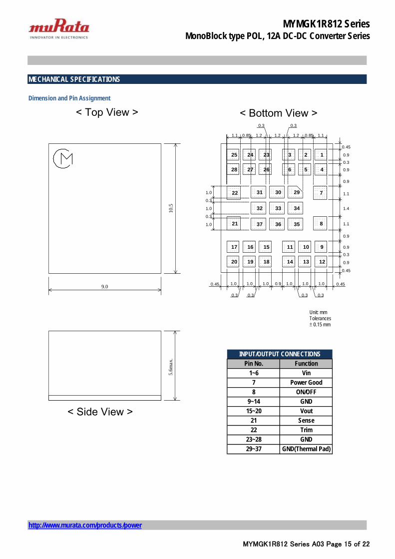
MECHANICAL SPECIFICATIONS
Dimension and Pin Assignment
http://www.murata.com/products/power
GND
Function1~6 Vin
29~37 GND(Thermal Pad)
7 Power Good8 ON/OFF
9~14 GND15~20
INPUT/OUTPUT CONNECTIONS
23~28
21 Sense22 Trim
Vout
Pin No.
9.0
10.5
5.6m
ax.
123
456
232425
262728
91011
121314
151617
181920
8
7
21
22
1.01.01.00.9
0.3
0.451.01.01.00.45
0.30.3 0.3
31 30
32 33 34
1.10.851.21.21.20.851.1
0.30.3
0.45
353637
29
0.9
0.3
0.9
1.1
0.9
1.4
1.1
0.9
0.9
0.3
0.9
0.45
1.0
0.3
1.0
0.3
1.0
Unit: mmTolerances ± 0.15 mm
< Bottom View >< Top View >
< Side View >

MYMGK1R812 SeriesMonoBlock type POL, 12A DC-DC Converter Series
MYMGK1R812 Series A03 Page 16 of 22
Recommended Board Land Pattern (Top View)
Unit: mm
Example of Pattern Layout (Top View) PictureTOP VIEW
BOTTOM VIEW
http://www.murata.com/products/power
20.9x11.0(mm)
1.11.11.10.8
0.2
0.41.11.11.10.4
0.20.2 0.2
1.20.751.31.31.30.751.2
0.20.2
0.4
1.0
0.2
1.0
1.2
0.8
1.3
1.2
0.8
1.0
0.2
1.0
0.4
1.1
0.2
1.1
0.2
1.1
3.4
3.4
1 2
8
9
7
3
4 5 6
10 11
12 13
21
201918
171615
14
22
23 24 25
26 27 28
29 30 31
323334
35 36 37
0.75
0.55
MYMGK1R812 SeriesMonoBlock type POL, 12A DC-DC Converter Series
MYMGK1R812 Series A03 Page 17 of 22
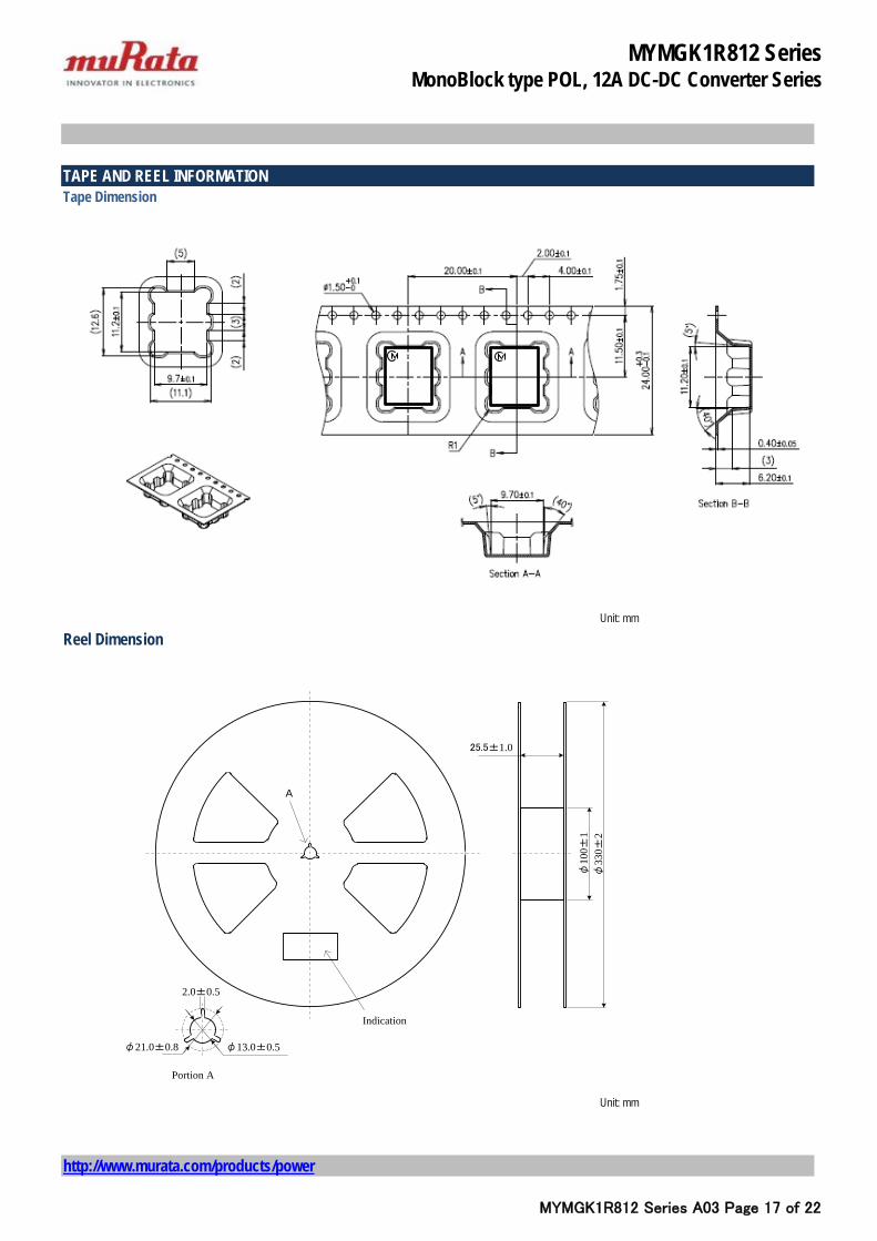
TAPE AND REEL INFORMATIONTape Dimension
Unit: mm
Reel Dimension
Unit: mm
http://www.murata.com/products/power
φ33
0±2
φ10
0±1
25.5±1.0
φ13.0±0.5φ21.0±0.8
Portion A
Indication
A
2.0±0.5

MYMGK1R812 SeriesMonoBlock type POL, 12A DC-DC Converter Series
MYMGK1R812 Series A03 Page 18 of 22
TAPE SPECIFICATION
Note
http://www.murata.com/products/power
Part Number Qty(pcs)MYMGK1R812FRSR 400MYMGK1R812ERSR 400
MYMGK1R812FRSRD 100MYMGK1R812ERSRD 100
1. The adhesive strength of the protective tape must be within 0.1-1.3N.2.Each reel contains the quantities such as the table below.3.Each reel set in moisture-proof packaging because of MSL 3.4.No vacant pocket in “Module on tape” section.5.The reel is labeled with Murata part number and quantity.
Circle Hole
Pulling DirectionM M
No.1 Pin
Empty portion(200mm MIN)
Empty portion(180mm MIN)
Leader portion(200mm MIN)
"Module on tape" portion
Indication

MYMGK1R812 SeriesMonoBlock type POL, 12A DC-DC Converter Series
MYMGK1R812 Series A03 Page 19 of 22
http://www.murata.com/products/power
TECHNICAL NOTES
COPPER STRIP
GND
VOUT
SCOPEC1 C2 RLOA
COPPERSTRIP
3-7mm
Input FuseCertain applications and/or safety agencies may require fuses at the inputs of power conversion components. Fuses should also be used when there is the possibility of sustained input voltage reversal which is not current limited. For greatest safety, we recommend a fast blow fuse installed in the ungrounded input supply line. The installer must observe all relevant safety standards and regulations. For safety agency approvals, install the converter in compliance with the end-user safety standard.Input Under-Voltage Shutdown and Start-Up ThresholdUnder normal start-up conditions, converters will not begin to regulate properly until the ramping-up input voltage exceeds and remains at the Start-Up Threshold Voltage (see Specifications). Once operating, converters will not turn off until the input voltage drops below the Under-Voltage Shutdown Limit. Subsequent restart will not occur until the input voltage rises again above the Start-Up Threshold. This built-in hysteresis prevents any unstable on/off operation at a single input voltage.Users should be aware however of input sources near the Under-Voltage Shutdown whose voltage decays as input current is consumed (such as capacitor inputs), the converter shuts off and then restarts as the external capacitor recharges. Such situations could oscillate. To prevent this, make sure the operating input voltage is well above the UV Shutdown voltage at all times.Start-Up TimeAssuming that the output current is set at the rated maximum, the Vin to Vout Start-Up Time (see Specifications) is the time interval between the point when the ramping input voltage crosses the Start-Up Threshold and the fully loaded regulated output voltage enters and remains within its specified accuracy band. Actual measured times will vary with input source impedance, external input capacitance, input voltage slew rate and final value of the input voltage as it appears at the converter.These converters include a soft start circuit to moderate the duty cycle of its PWM controller at power up, thereby limiting the input inrush current.The On/Off Remote Control interval from On command to Vout regulated assumes that the converter already has its input voltage stabilized above the Start-Up Threshold before the On command. The interval is measured from the On command until the output enters and remains within its specified accuracy band. The specification assumes that the output is fully loaded at maximum rated current. Similar conditions apply to the On to Vout regulated specification such as external load capacitance and soft start circuitry.Recommended Input FilteringThe user must assure that the input source has low AC impedance to provide dynamic stability and that the input supply has little or no inductive content, including long distributed wiring to a remote power supply. For best performance, we recommend installing a low-ESR capacitor immediately adjacent to the converter’s input terminals.
The capacitor should be a ceramic type such as the Murata GRM32 series and a electrolytic type such as Panasonic OS-CON series. Initial suggested capacitor values are 22 uF x 2 or 47uF x 2 ceramic type and 1000uF x 1 electrolytic type , rated at twice the expected maximum input voltage. Make sure that the input terminals do not go below the under voltage shutdown voltage at all times. More input bulk capacitance may be added in parallel (either electrolytic or tantalum) if needed.Recommended Output FilteringThe converter will achieve its rated output ripple and noise with additional external capacitor. The user may install more external output capacitance reduce the ripple even further or for improved dynamic response. Again, use low-ESR ceramic (Murata GRM32 series). Initial values of 220 uF x 3 ceramic type may be tried, either single or multiple capacitors in parallel. Mount these close to the converter. Measure the output ripple under your load conditions. Use only as much capacitance as required to achieve your ripple and noise objectives. Excessive capacitance can make step load recovery sluggish or possibly introduce instability. Do not exceed the maximum rated output capacitance listed in the specifications.Output NoiseAll models in this converter series are tested and specified for output noise using designated external output components, circuits and layout as shown in the figures below. In the figure below, the two copper strips simulate real-world printed circuit impedances between the power supply and its load. In order to minimize circuit errors and standardize tests between units, scope measurements should be made using BNC connectors or the probe ground should not exceed one half inch and soldered directly to the test circuit.
C1=220uF x 3 CERAMICC2=OPENFigure :Measuring Output Ripple and Noise
Minimum Output Loading RequirementsAll models regulate within specification and are stable under no load to full load conditions. Operation under no load might however slightly increase output ripple and noise.Thermal ShutdownTo prevent many over temperature problems and damage, these converters include thermal shutdown circuitry. If environmental conditions cause the temperature of the converter’s to rise above the Operating Temperature Range up to the shutdown temperature, an on-board electronic temperature sensor will power down the unit. When the temperature decreases below the turn-on threshold, the converter will automatically restart.

MYMGK1R812 SeriesMonoBlock type POL, 12A DC-DC Converter Series
MYMGK1R812 Series A03 Page 20 of 22
http://www.murata.com/products/power
CAUTION: If you operate too close to the thermal limits, the converter may shut down suddenly without warning. Be sure to thoroughly you’re your application to avoid unplanned thermal shutdown.Temperature Derating CurvesThe graphs in this data sheet illustrate typical operation under a variety of conditions. The derating curves show the maximum continuous ambient air temperature. Note that these are AVERAGE measurements. Note that the temperatures are of the ambient airflow, not the converter itself which is obviously running at higher temperature than the outside air. Also note that very low flow rates (below about 25 LFM) are similar to “natural convection,” that is, not using fan-forced airflow. Murata makes Characterization measurements in a closed cycle wind tunnel with calibrated airflow. We use both thermocouples and an infrared camera system to observe thermal performance.CAUTION: These graphs are all collected at slightly above Sea Level altitude. Be sure to reduce the derating for higher density altitude.Output Current LimitingCurrent limiting inception is defined as the point at which full power falls below the rated tolerance. See the Performance/Functional Specifications. Note particularly that the output current may briefly rise above its rated value in normal operation as long as the average output power is not exceeded. This enhances reliability and continued operation of your application. If the output current is too high, the converter will enter the short circuit condition.Output Short Circuit ConditionWhen a converter is in current-limit mode, the output voltage will drop as the output current demand increases. Following a time-out period, the converter will restart, causing the output voltage to begin ramping up to its appropriate value. If the short-circuit condition persists, another shutdown cycle will initiate. This rapid on/off cycling is called “hiccup mode”. The hiccup cycling reduces the average output current, thereby preventing excessive internal temperatures and/or component damage. A short circuit can be tolerated indefinitely.The “hiccup” system differs from older latching short circuit systems because you do not have to power down the converter to make it restart. The system will automatically restore operation as soon as the short circuit condition is removed.
UVP/OVP FunctionThis product monitors a resistor divided feedback voltage to detect over and under voltage. When the feedback voltage becomes lower than 70% of the target voltage, after 1ms, the product latches OFF. The converter restarts after a hiccup delay (about 16 ms ). This function is enabled 1.5ms after the soft-start is completed. When the feedback voltage becomes higher than 120% of the target voltage, the circuit operates sink-mode to decrease output voltage. If the output voltage reaches UV threshold, the device restarts after a hiccup delay. If the OV condition remains, the converter will not start until the OV condition is removed. Remote On/Off ControlPlease refer to the Connection Diagram on page 1 for On/Off connections.Positive logic models are enabled when the On/Off pin is left open or is pulled high to Vin with respect to GND. An internal bias current causes the OVP open pin to rise to Vin. Positive-polarity devices are disabled when the On/Off is grounded or brought to within a low voltage (see Specifications) with respect to GND.Dynamic control of the On/Off function should be able to sink appropriate signal current when brought low and withstand appropriate voltage when brought high. Be aware too that there is a finite time in milliseconds (see Specifications) between the time of On/Off Control activation and stable, regulated output. This time will vary slightly with output load type and current and input conditions.Output Capacitive LoadUsers should only consider adding capacitance to reduce switching noise and/or to handle spike current load steps. Install only enough capacitance to achieve noise objectives. Excess external capacitance may cause regulation problems, degraded transient response and possible oscillation or instability.Soldering GuidelinesMurata recommends the specifications below when installing these converters. These specifications vary depending on the solder type.Exceeding these specifications may cause damage to the product. Your production environment may differ therefore please thoroughly review these guidelines with your process engineers.This product can be reflowed once.
Output Voltage Remote SenseThis function is capable to compensate up the voltage drop between the output and input of load. The voltage of the Vout pin musu NOT be over their allowed maximum voltage if using the remote sense. The sense trace should be connected to Vout line as shortly as possible. The sense trace should be shielded by GND line or something else to reduce noise pickup.The sense line length is recommended within 10cm for output voltage stability.If the remote sense is not needed, the Sense pin should be connected to the Vout pin directly.

MYMGK1R812 SeriesMonoBlock type POL, 12A DC-DC Converter Series
MYMGK1R812 Series A03 Page 21 of 22
http://www.murata.com/products/power
Mother Substrate
Converter
Preheat Temperature Less than 1degC per secondTime over Liquidus 45 to 75 secondsMaximum Peak Temperature 250degCCooling Rate Less than 3degC per second
Preheat Temperature Less than 1degC per secondTime over Liquidus 60 to 75 secondsMaximum Peak Temperature 235degCCooling Rate Less than 3degC per second
Reflow Solder Operations for surface-mount productsFor Sn/Ag/Cu based solders:
For Sn/Pb based solders:
Output voltage depends on the value of capacitance of Cout in this product , the smaller Cout may cause the higher output voltage. The equations above are only reference, so please check output voltage and adjust Rtrim in user circumstances. To increase(decrease) output voltage is obtained by decreasing(increasing) value of Rtrim .
Output Voltage AdjustmentThe output voltage may be adjusted over a limited range by connecting an external trim resistor (Rtrim) between the Trim pin and GND pin. The Rtrim resistor must be a 1/10W precision metal film type,±0.5% accuracy or better with low temperature coefficient, ±100 ppm/degC. or better. Mount the resistor close to the converter with very short leads or use a surface mount trim resistor.In the table below, the estimated resistance is given at limited condition ;Vin:typ.,Ta:25degC,Iout:max.,Cout:660uF. (Please look at Test Circuit which is shown on appendix page). Do not exceed the specified limits of the output voltage or the converter’s maximum power rating when applying these resistors. Also, avoid high noise at the Trim input. However, to prevent instability, you should never connect any capacitors between Trim pin and GND pin.
Resistor Trim Equation
Pb-free solder processesFor Pb-free solder processes, the product is qualified for MSL 3 according to IPC/JEDEC standard J-STD-020C.During reflow the converter must not exceed 250 degC at any time.
Dry Pack InformationProducts intended for Pb-free reflow soldering processes are delivered in standard moisture barrier bags according to IPC/JEDEC standard J-STD-033.(Handling, packing, shipping and use of moisture/reflow sensitivity surface mount devices.)Using products in high temperature Pb-free soldering processes requires dry pack storage and handling. In case the products have been stored in an uncontrolled environment and no longer can be considered dry, the modules must be baked according to J-STD-033.
Recommended Lead-free Solder Reflow Profile
CAUTION: Do not reflow the converter as follows,because the converter may fall from the substrate
during reflowing.
Output Voltage MYMGK1R812FRSR MYMGK1R812ERSR0.7V 75+0.36 68+2.41.0V 16+0.39 161.2V 10+0.75 10+0.621.5V 6.8+0.33 6.8+0.241.8V 5.1+0.27 5.1+0.20
Estimated Rtrim (kohm)
Power Good(P.G)These products has power-good output that indicates high when switcher output is within the target. Thepower-good function is activated after soft-start has finished. If the output voltage becomes within +10%and –5% of the target value, internal comparators detect power-good state and the power-good signal becomeshigh after a 1-ms internal delay. If the output voltage goes outside of +15% or –10% of the target value, thepower-good signal becomes low after two microsecond (2-μs) internal delay. The power-good output is an opendrain output and must be pulled up internally.
MYMGK1R812FRSR
A = 0.617 + 0.01 x ( Vout - 0.6 )
MYMGK1R812ERSR
A = 0.612 + 0.01 x ( Vout - 0.6 )
Rtrim ( kohm ) = 10 x A
( Vout - A )
Rtrim ( kohm ) = 10 x A
( Vout - A )

MYMGK1R812 SeriesMonoBlock type POL, 12A DC-DC Converter Series
MYMGK1R812 Series A03 Page 22 of 22
APPENDIX
Test Circuit
http://www.murata.com/products/power Specifications are subject to change without notice.
RLVin
Vin
GND
ON/OFF
C2
C3
Vout
Rtrim
Trim
Power Good
C1
Sense
Do not connect any additional components between the Trim pin and Vout or between the Trimand Sense pins. Use only the specified connections.If there is a long inductive cable length between the input power source and converter, then some additional bulk decoupling capacitance (eg. up to 1000uF) may be necessary to ensure a low AC impedance power source.This would typically be aluminum electrolytic type and does not need to be close to the input terminals of converter.
This product is subject to the following operating requirementsand the Life and Safety Critical Application Sales Policy:Refer to: https://power.murata.com/en/requirements
Murata Manufacturing Co., Ltd makes no representation that the use of its products in the circuits describherein, or the use of other technical information contained herein, will not infringe upon existing or futurepatent rights. The descriptions contained herein do not imply the granting of licenses to make, use,or sell equipment constructed in accordance therewith. Spec and cautions are subject to changewithout notice. © 2018 Murata Manufacturing Co., Ltd
!
Vin:DC Power SupplyRL:Electronic Load Device
For MYMGK1R812FRSR 4.5≤Vin(V)≤5.5C1:1000uF/25V x 1pc Electrolysis CapacitorC2:47uF/10V x 2pcs (GRM32ER71A476KE15:Murata) C3:220uF/4V x 3pcs (GRM32EC80G227ME05:Murata)
For MYMGK1R812FRSR 5.5<Vin(V)≤8.0C1:1000uF/25V x 1pc Electrolysis Capacitor C2:22uF/25V x 2pcs (GRM32ER71E226KE15 : Murata) C3:220uF/4V x 3pcs (GRM32EC80G227ME05:Murata)
For MYMGK1R812ERSR 8.0≤Vin(V)≤15.0C1:1000uF/25V x 1pc Electrolysis CapacitorC2:22uF/25V x 2pcs (GRM32ER71E226KE15:Murata) C3:220uF/4V x 3pcs (GRM32EC80G227ME05:Murata)