molecular-dynamics simulations of stacking-fault-induced
TRANSCRIPT
University of Massachusetts AmherstScholarWorks@UMass Amherst
Physics Department Faculty Publication Series Physics
2009
Molecular-dynamics Simulations of Stacking-fault-induced Dislocation Annihilation in Pre-strainedUltrathin Single-crystalline Copper FilmsKedarnath KolluriUniversity of Massachusetts - Amherst
M. Rauf GungorUniversity of Massachusetts - Amherst
Dimitrios MaroudasUniversity of Massachusetts - Amherst
Follow this and additional works at: https://scholarworks.umass.edu/physics_faculty_pubs
Part of the Physics Commons
This Article is brought to you for free and open access by the Physics at ScholarWorks@UMass Amherst. It has been accepted for inclusion in PhysicsDepartment Faculty Publication Series by an authorized administrator of ScholarWorks@UMass Amherst. For more information, please [email protected].
Recommended CitationKolluri, Kedarnath; Gungor, M. Rauf; and Maroudas, Dimitrios, "Molecular-dynamics Simulations of Stacking-fault-inducedDislocation Annihilation in Pre-strained Ultrathin Single-crystalline Copper Films" (2009). Physics Department Faculty PublicationSeries. 8.Retrieved from https://scholarworks.umass.edu/physics_faculty_pubs/8
1
Molecular-dynamics simulations of
stacking-fault-induced dislocation annihilation in
pre-strained ultrathin single-crystalline copper films
Kedarnath Kolluri, M. Rauf Gungor, and Dimitrios Maroudas*
Department of Chemical Engineering
University of Massachusetts, Amherst, MA 01003-3110
Abstract
We report results of large-scale molecular-dynamics (MD) simulations of dynamic
deformation under biaxial tensile strain of pre-strained single-crystalline nanometer-
scale-thick face-centered cubic (fcc) copper films. Our results show that stacking faults,
which are abundantly present in fcc metals, may play a significant role in the
dissociation, cross-slip, and eventual annihilation of dislocations in small-volume
structures of fcc metals. The underlying mechanisms are mediated by interactions within
and between extended dislocations that lead to annihilation of Shockley partial
dislocations or formation of perfect dislocations. Our findings demonstrate dislocation
starvation in small-volume structures with ultra-thin film geometry, governed by a
mechanism other than dislocation escape to free surfaces, and underline the significant
role of geometry in determining the mechanical response of metallic small-volume
structures.
*To whom correspondence should be addressed. E-mail: [email protected]
2
I. Introduction
A broad range of modern technologies relies increasingly on the use of
nanometer-scale-thick metallic films. Typically, over 500 processes are involved in the
development of micro- and nano-scale devices. During these processes, the constituent
materials are subjected to various thermo-mechanical environments, which introduce
strain in the nano-scale-thick metallic films, causing them to undergo plastic deformation.
Such materials response to strain has significant impact on the ductility, hardness, and
strength of the metallic films and may lead eventually to their failure; the mechanical
response of device interconnects in microelectronics offers typical examples.1-4
The
mechanical behavior of single-crystalline metallic materials undergoing plastic
deformation is a direct consequence of the nucleation and motion of dislocations, as well
as a variety of dislocation-dislocation interactions. For bulk materials, such mechanisms
are well understood and phenomenological models have been developed for their
deformation. These phenomenological models, however, cannot be extended to the
nanoscale and, more specifically, to describing mechanical response of ultra-thin metallic
films.
Unlike bulk metals, metallic nanostructures and other small-volume structures
exhibit, for example, ultra-high strength. Examples range from whiskers with small
diameters that were reported (as early as almost 6 decades ago) to have much higher
strength than bulk metals5,6
to the uniaxial compression of nanometer-scale pillars of
face-centered cubic (fcc) metals that yielded flow strengths comparable to the materials’
ideal shear strength.7-11
In bulk metals subjected to external stress, work hardening is
caused by an increase in the dislocation density and by a sharp decrease in plastic flow;
the former is due to rapid dislocation multiplication through double cross-slip and Frank-

3
Read-type mechanisms, while the latter is due to interactions between dislocations in
multiple slip planes that lead to the formation of sessile dislocations that act as barriers to
dislocation motion, as well as due to pile-up of dislocations at obstacles such as grain
boundaries and sessile dislocations. In metallic nano-meter-thick films and (in general)
small-volume structures, however, it has been argued that depletion of dislocations
causes the observed ultra-high strength.7-13
For example, in compression experiments of
Ni single-crystalline nanopillars with a high initial dislocation density, the dislocation
density always decreased during the application of strain;11
subsequently, the nearly
defect-free crystal deformed elastically until new dislocations nucleated. In ultra-thin
metallic films, a fundamental understanding of the atomistic mechanisms of deformation
dynamics is essential for accurate property predictions, better reliability analysis, and
design of higher-quality devices. The deformation mechanisms, however, are
particularly difficult to study experimentally; for example, in high-strain-rate deformation
of single-crystalline fcc metals such as Cu, certain strain relaxation time scales are in the
sub-nanosecond range.14
Atomic-scale and other fine-scale dynamical simulation
methods provide ideal means for analyzing the deformation mechanisms in ductile thin
films by direct monitoring of the dynamical response of the materials at the
atomic/microscopic scale.15,16
First-principles density-functional-theory calculations and large-scale molecular-
dynamics (MD) simulations have been used extensively toward a fundamental
understanding of plastic flow initiation and nucleation of dislocations, as well as
investigations of plastic deformation during nanoindentation of metal surfaces.17,18
These
techniques also have been used to explore and analyze dislocation intersections,19,20
deformation processes at shock loading conditions in metallic bulk21
and thin-film22-24
4
materials, as well as amorphization of fcc crystalline metallic nanowires under strain-
rate-limited shock loading at controlled temperatures.25
In addition, discrete dislocation-
dynamics simulations have been used to study size effects in nanopillars of fcc metals;
these simulations of fcc nanopillars have shown that dislocation escape through the free
surfaces and depletion or inactivation of dislocation sources play a significant role in the
plastic response of small-volume structures.13,26-28
The fundamental mechanisms of
dislocation interactions and their possible annihilation in ultra-thin metallic films,
however, remain largely unexplored and, therefore, elusive.
In this article, we report results of an atomic-scale analysis of dislocation-
dislocation interaction mechanisms based on MD simulations of dynamic deformation of
free-standing single-crystalline ultra-thin fcc copper films. The thin-film samples used in
our analysis were pre-strained to introduce dislocations, consistently with samples used in
experimental studies of the mechanical behavior of small-volume structures that had a
high initial dislocation density.11
Our results indicate that the interactions within and
between simple extended dislocations, each of which consists of two Shockley partial
dislocations with complementary Burgers vectors separated by a stacking fault, may
contribute significantly to dislocation depletion in nanometer-scale fcc metals. We
identify different classes of stacking fault-dislocation interactions and present a detailed
analysis of dislocation depletion in these films mediated by these mechanisms. Our
findings suggest that dislocation escape to free surfaces may not be the primary
mechanism of dislocation depletion in small-volume structures of fcc metals with ultra-
thin film geometry.
The article is structured as follows. The simulation methods and analysis
techniques employed in this study are discussed in Sec. II. The results of our

5
computational analysis, which includes the mechanical behavior of the thin films and the
underlying physical mechanisms, are presented in Sec. III. The results of the analysis are
discussed in Sec. IV in the context of earlier experimental studies on nanopillars and
computational studies of interactions between dislocations and twin boundaries. The
limitations of our simulations also are discussed in Sec. IV. Finally, the main
conclusions of our study are summarized in Sec. V.
II. Simulation Methods and Analysis of Simulation Results
In our MD simulations, we employed slab supercells consisting of single-
crystalline copper films with periodic boundary conditions applied in the x- and y-
directions in a Cartesian representation; the film planes were oriented normal to the z
axis. Vacuum space above the top and below the bottom surfaces of the films was used
in order to generate free surfaces and mimic free-standing thin films. The Cartesian x, y,
and z axes were taken along the [110] , [112] , and [111] crystallographic directions,
respectively, with the film plane corresponding to the (111) crystallographic plane. For
the results reported here, we employed two different simulation cells: one that contained
1,520,640 Cu atoms (with an edge size of 61.35, 63.76, and 4.38 nm in the x-, y-, and z-
direction, respectively) and another one that contained 1,548,797 Cu atoms (with an edge
size of 40.90, 38.96, and 11.27 nm in the x-, y-, and z-direction, respectively); in both
cases, the reported cell dimensions correspond to the unstrained state of the metallic thin
film.
The interatomic interactions were modeled using an embedded-atom-method
(EAM) potential, parameterized for copper.29
This potential was validated by comparison
6
of its predictions with those of ab initio calculations.30
For our MD simulations of thin-
film dynamic deformation under biaxial tensile strain, we used the public-domain
computer software LAMMPS.31
In our simulations, the temperature was kept constant at T
= 100 K by explicitly rescaling the atomic velocities at each time step. In the MD
simulations of thin-film dynamic deformation under biaxial tensile strain, all the films
used were pre-treated before conducting the MD simulations of dynamical straining in
order to generate the initial dislocation distributions. Specifically, the thin films were
pre-strained in biaxial tension to a specified strain level at a constant true strain rate of
2.01 ! 1011
s-1
(equally in each lateral direction). Under this mode of loading, three
{111} crystallographic planes are activated; the Schmidt factor for all possible slip
directions in the (111) plane, which is also the orientation of the thin film surface, is
negligibly small. After the desired strain level was reached, isothermal-isostrain MD
simulations were performed in order to equilibrate the thin-film structure. We analyzed
the mechanical response of three thin-film samples; two of these, samples 1 and 2, had
initial (unstrained-state) thicknesses of 4.38 nm and 11.27 nm, respectively. The third
one, sample 3, was prepared by compressing sample 1 after its tensile straining back to its
original lateral dimensions at the same constant high strain rate and then equilibrating the
film’s structure by isothermal-isostrain MD simulation. In their pre-treatment, the thin-
film samples discussed in this article were subjected to biaxial tensile strain at a level of
8%. For pre-treatment under biaxial tensile strain at strain levels over the range from 6%
to 10%, the resulting microstructure of the equilibrated thin films remained qualitatively
identical. The final thicknesses of samples 1, 2, and 3 were 3.84 nm, 9.76 nm, and 4.43
nm, respectively.
These samples contained predominantly simple extended dislocations that either
7
extended across the film thickness or were threading dislocation half loops emanating
from the film surfaces. The initial dislocation density, ! , of these films ranged from 1.0
! 1017
m-2
to 3.2 ! 1017
m-2
; ! = l/V where l is the total length of all the dislocations in the
film and V is the film’s volume. In samples 1 and 3, many extended dislocations spanned
across the film thickness, while only a few threading dislocation half loops were present.
In the thicker film, however, the population of threading dislocation half loops was
comparable with that of the extended dislocations that spanned across the film thickness.
We note that this initial film microstructure is similar to that of the Ni nanopillars used in
mechanical annealing experiments;11
in those experiments, similar dislocation types were
observed, i.e., most of them extended across the thickness of the nanopillar and a few of
them were threading dislocation half loops at the surface of the nanopillar, and the
dislocation density was ~ 1015
m-2
. After this film pre-treatment stage, the final steady-
state values of the von Mises shear stress, "vM, for samples 1, 2, and 3 were 530, 460, and
105 MPa, respectively; "vM is defined as the second invariant of the stress tensor and is
given by !vM
=1
6(!
xx" !
yy)2+ (!
yy" !
zz)2+ (!
zz" !
xx)2+ 6(!
xy
2+!
yz
2+!
zx
2) , where "#$ (#, $ = x, y,
or z) are the elements of the stress tensor. Although the stresses in the thin films were
significant, most of the stress was due to elastic straining. In the thin films studied here,
the shear strain, measured as the second invariant of the local atomic strain tensor,32
varied between 0.7% and 1.59%; this indicates that in these pre-treated thin films the
applied biaxial strain had relaxed significantly. Additionally, the pre-treatment
equilibration stage was continued until ensemble averages of the stress and potential
energy in the thin films reached constant (i.e., steady) values. Following pre-treatment,
the samples were strained biaxially in tension at a constant strain rate of 7 ! 108
s-1
(again
8
equally in each lateral direction) and the evolution of the film structure was monitored in
detail.
For monitoring the structural response of the thin film to the applied biaxial strain,
we employed common neighbor analysis (CNA) in order to identify atoms in locally
perfect hexagonal close-packed (hcp) and fcc lattice arrangements.33
We used the public-
domain computer software ATOMEYE 32
in order to visualize sequences of MD-generated
atomic configurations. Atoms with 12 nearest neighbors (coordination number for
perfect fcc and hcp lattices) that are not in locally perfect fcc or hcp lattice arrangements
are located in the dislocation cores; in our analysis, we have identified these “non-
coordination lattice defects” as a means of dislocation visualization. The dislocation
densities computed in our simulations, on the order of 1016
- 1017
m-2
, are one to four
orders of magnitude higher than those observed typically in experiments; such high
dislocation densities are typical of MD simulations.
The stress in the material was calculated using the Virial formula.34
We
implemented two methods for the computation of the film’s volume (involved in both the
stress and the dislocation density computation). In the first method, we constructed on the
thin-film surface a grid of multiple elements of known lateral dimensions; we computed
the thickness of each such element as the distance, in z, between the two atoms on the
opposite surfaces of the film that were the farthest located from its center plane on each
surface within the element. The total volume of the film was then computed as the sum
of the element volumes. In the second method, we estimated the thickness of the film as
the distance, in z, between the two atoms on each of the opposite film surfaces that were
the farthest located from the center plane of the film. The first method underestimates the
total film volume, while the second method overestimates it. The stress values reported

9
in the stress-strain curve plots of this article were computed using the second method.
Irrespective of the method used for film volume computation, the corresponding
qualitative features of the stress evolution in dynamic deformation remained identical
except at a stage close to failure; at this stage, the volume computed according to the first
method excludes (incorrectly) the pits formed on the surface. The difference in the stress
values computed by the two methods were ~100-200 MPa; the first method yielded
consistently higher stress values.
III. Mechanical Behavior and Underlying Physical Mechanisms
Figure 1(a) shows the evolution of the von Mises shear flow stress, "vM,
dislocation density, !, and the stacking fault area, Asf, in sample 1 (initial ! = 1.4 ! 1017
m-2
) during dynamical biaxial straining, where the applied strain level, ", increases
linearly with time. The stacking fault area is defined as A
sf= (N
hcp/ 2) ! (1 / 3) ! (3 3a2 / 4) ,
where the first factor is the number of hcp atoms on one of the two planes of the stacking
fault, the second factor is the number of atoms per hexagonal unit of the stacking-fault
lattice plane, and the third factor is the area of each such hexagonal unit. The decrease in
! and Asf until they each reach a minimum value indicates annihilation of dislocations.
Subsequently, new dislocations nucleate, leading to an increase in ! and Asf. From the
shear stress-strain curve, it is evident that the thin film does not undergo stage-II
hardening, which is typical of bulk metals. The maximum "vM computed in our
simulations varied between 1.56 and 1.74 GPa. These stress levels are 39.9%-44.5% of
the ideal simple shear strength of our copper model (3.91 GPa according to the
10
interatomic potential employed in our MD simulations, which compares well with first-
principles calculations30
); we also note that these stress levels are consistent with
experimental measurements on Au nanopillars (indicating that the nanopillars reached
44% of the material’s theoretically predicted ideal pure shear strength12
).
The mechanical response of the thin film to the applied biaxial strain exhibits
three different stages; these stages are indicated in Fig. 1(a) and are termed as Stage I,
Stage II, and Stage III. Figure 1(b) shows three-dimensional views of the MD simulation
cell at various states, which are also marked in Fig. 1(a). In Stage I, "vM increases rapidly
to about 1.1 GPa. The glide of most dislocations is activated in this stage. A few partial
dislocations retract into the extended dislocations that they constitute and, in the process,
they unzip the stacking faults that they bound. Such dislocation glide induces the
interaction of the two Shockley partial dislocation components of a simple extended
dislocation, resulting in a reduction of the stacking-fault area. The reduced stacking-fault
area increases the mobility of the dislocations. In addition to the reduction in stacking-
fault area, a few dislocations also annihilate in Stage I, primarily due to interactions
between extended dislocations and, to a far lesser extent, due to interactions between
partials and anti-partials that bind a few stacking faults. Dislocation annihilation due to
interactions between partial and anti-partial dislocations occurs possibly because such
dislocations are unstable. In Stage II, for 1.5% < " < 4.5% [Fig. 1(a)], ! and Asf decrease
to less than one third of their initial values; "vM, however, remains nearly constant. Stage
II is dominated by dislocation glide and, more importantly, by interactions within and
between extended dislocations. The intersection of the gliding dislocations with the
stacking faults of the extended dislocations causes cross-slip of the intersecting
dislocations and break-up of the obstacle stacking faults. At least one of the dislocations
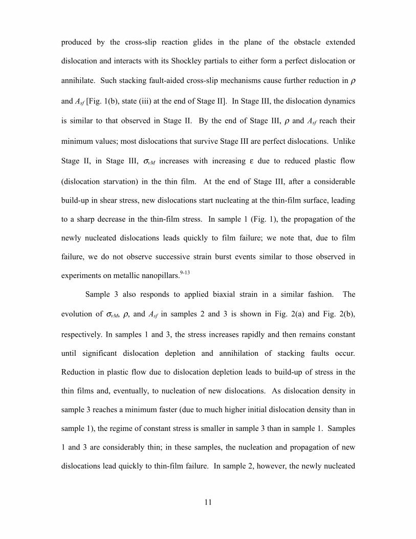
11
produced by the cross-slip reaction glides in the plane of the obstacle extended
dislocation and interacts with its Shockley partials to either form a perfect dislocation or
annihilate. Such stacking fault-aided cross-slip mechanisms cause further reduction in !
and Asf [Fig. 1(b), state (iii) at the end of Stage II]. In Stage III, the dislocation dynamics
is similar to that observed in Stage II. By the end of Stage III, ! and Asf reach their
minimum values; most dislocations that survive Stage III are perfect dislocations. Unlike
Stage II, in Stage III, "vM increases with increasing " due to reduced plastic flow
(dislocation starvation) in the thin film. At the end of Stage III, after a considerable
build-up in shear stress, new dislocations start nucleating at the thin-film surface, leading
to a sharp decrease in the thin-film stress. In sample 1 (Fig. 1), the propagation of the
newly nucleated dislocations leads quickly to film failure; we note that, due to film
failure, we do not observe successive strain burst events similar to those observed in
experiments on metallic nanopillars.9-13
Sample 3 also responds to applied biaxial strain in a similar fashion. The
evolution of "vM, !, and Asf in samples 2 and 3 is shown in Fig. 2(a) and Fig. 2(b),
respectively. In samples 1 and 3, the stress increases rapidly and then remains constant
until significant dislocation depletion and annihilation of stacking faults occur.
Reduction in plastic flow due to dislocation depletion leads to build-up of stress in the
thin films and, eventually, to nucleation of new dislocations. As dislocation density in
sample 3 reaches a minimum faster (due to much higher initial dislocation density than in
sample 1), the regime of constant stress is smaller in sample 3 than in sample 1. Samples
1 and 3 are considerably thin; in these samples, the nucleation and propagation of new
dislocations lead quickly to thin-film failure. In sample 2, however, the newly nucleated
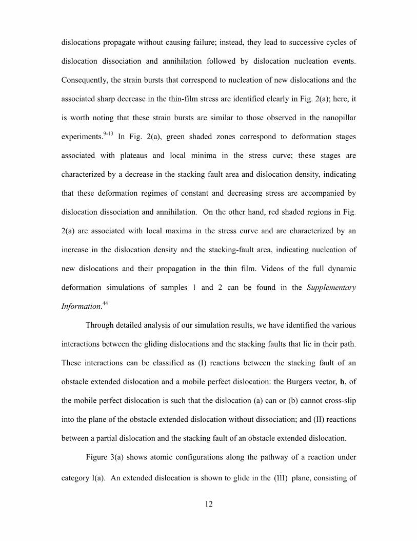
12
dislocations propagate without causing failure; instead, they lead to successive cycles of
dislocation dissociation and annihilation followed by dislocation nucleation events.
Consequently, the strain bursts that correspond to nucleation of new dislocations and the
associated sharp decrease in the thin-film stress are identified clearly in Fig. 2(a); here, it
is worth noting that these strain bursts are similar to those observed in the nanopillar
experiments.9-13
In Fig. 2(a), green shaded zones correspond to deformation stages
associated with plateaus and local minima in the stress curve; these stages are
characterized by a decrease in the stacking fault area and dislocation density, indicating
that these deformation regimes of constant and decreasing stress are accompanied by
dislocation dissociation and annihilation. On the other hand, red shaded regions in Fig.
2(a) are associated with local maxima in the stress curve and are characterized by an
increase in the dislocation density and the stacking-fault area, indicating nucleation of
new dislocations and their propagation in the thin film. Videos of the full dynamic
deformation simulations of samples 1 and 2 can be found in the Supplementary
Information.44
Through detailed analysis of our simulation results, we have identified the various
interactions between the gliding dislocations and the stacking faults that lie in their path.
These interactions can be classified as (I) reactions between the stacking fault of an
obstacle extended dislocation and a mobile perfect dislocation: the Burgers vector, b, of
the mobile perfect dislocation is such that the dislocation (a) can or (b) cannot cross-slip
into the plane of the obstacle extended dislocation without dissociation; and (II) reactions
between a partial dislocation and the stacking fault of an obstacle extended dislocation.
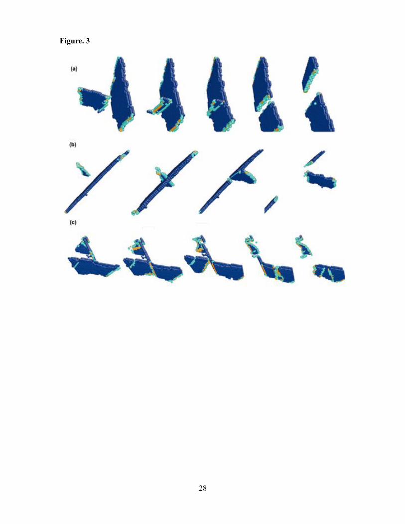
Figure 3(a) shows atomic configurations along the pathway of a reaction under
category I(a). An extended dislocation is shown to glide in the (111) plane, consisting of
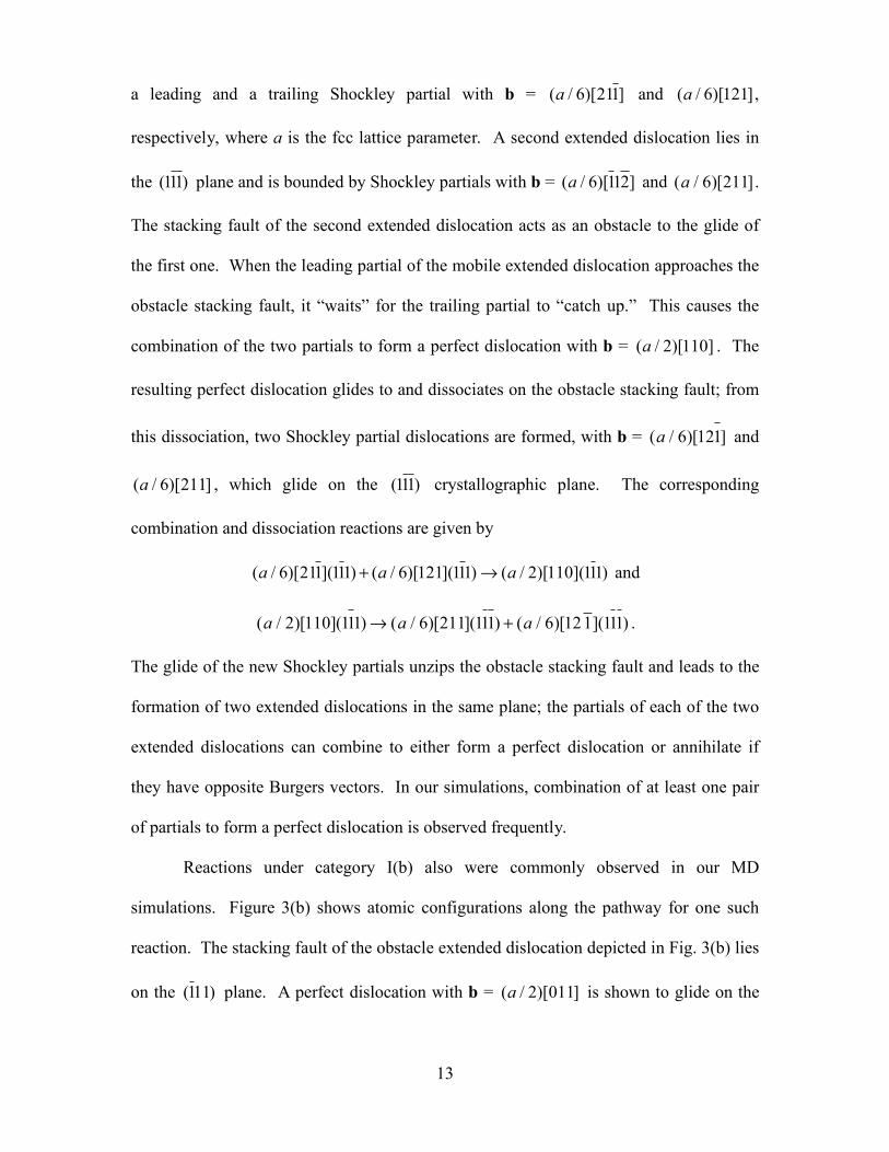
13
a leading and a trailing Shockley partial with b = ( / 6)[211]a and ( / 6)[121]a ,
respectively, where a is the fcc lattice parameter. A second extended dislocation lies in
the (111) plane and is bounded by Shockley partials with b = ( / 6)[112]a and (a / 6)[211] .
The stacking fault of the second extended dislocation acts as an obstacle to the glide of
the first one. When the leading partial of the mobile extended dislocation approaches the
obstacle stacking fault, it “waits” for the trailing partial to “catch up.” This causes the
combination of the two partials to form a perfect dislocation with b = ( / 2)[110]a . The
resulting perfect dislocation glides to and dissociates on the obstacle stacking fault; from
this dissociation, two Shockley partial dislocations are formed, with b = (a / 6)[121] and
( / 6)[211]a , which glide on the (111) crystallographic plane. The corresponding
combination and dissociation reactions are given by
( / 6)[211](111) ( / 6)[121](111) ( / 2)[110](111)a a a+ ! and
(a / 2)[110](111) ! (a / 6)[211](111) + (a / 6)[121](111) .
The glide of the new Shockley partials unzips the obstacle stacking fault and leads to the
formation of two extended dislocations in the same plane; the partials of each of the two
extended dislocations can combine to either form a perfect dislocation or annihilate if
they have opposite Burgers vectors. In our simulations, combination of at least one pair
of partials to form a perfect dislocation is observed frequently.
Reactions under category I(b) also were commonly observed in our MD
simulations. Figure 3(b) shows atomic configurations along the pathway for one such
reaction. The stacking fault of the obstacle extended dislocation depicted in Fig. 3(b) lies
on the (111) plane. A perfect dislocation with b = ( / 2)[011]a is shown to glide on the

14
(111) crystallographic plane toward the obstacle stacking fault. Upon intersecting with
the obstacle stacking fault, the perfect dislocation dissociates according to the
dissociation reaction
(a / 2)[011](111) ! (a / 6)[112](111) + (a / 6)[310]+ (a / 6)[211](111)
to form two Shockley partials, one in the plane of the gliding perfect dislocation and
another one in the plane of the obstacle stacking fault, and a sessile stair-rod dislocation
with b = ( / 6)[310]a . Subsequently, the produced stair-rod dislocation dissociates
according to the reaction
( / 6)[310] ( / 6)[121](111) ( / 6)[211](111)a a a! + .
The outcome of the two dissociation reactions is the formation of two extended
dislocations in the final state. In effect, upon interacting with the obstacle extended
dislocation, a perfect dislocation dissociates into its corresponding Shockley partials and
splits the obstacle extended dislocations into two extended dislocations. In our
simulations, we observe many reactions classified under category I(a) and I(b), which are
similar to the Friedel-Escaig cross-slip mechanism.35
Less frequently, we observe the dissociation of a Shockley partial at the stacking
fault of an obstacle extended dislocation. Figure 3(c) shows atomic configurations along
the pathway of one such reaction. The obstacle and the gliding extended dislocations lie
on the (111) and (111) crystallographic planes, respectively. The leading and the trailing
partials of the gliding extended dislocation have b = ( / 6)[112]a and (a / 6)[121] ,
respectively. Initially, the trailing partial of the gliding extended dislocation is entangled
with other dislocations and it is, therefore, unable to glide toward the leading partial,
combine with it, and form a perfect dislocation. Upon contact with the obstacle stacking
15
fault, the leading partial dissociates to generate a Shockley partial in the plane of the
obstacle stacking fault and a sessile stair-rod dislocation according to the reaction
(a / 6)[112](111) ! (a / 6)[112](111) + (a / 3)[100] .
The trailing partial of the gliding extended dislocation, which is now separated from the
entanglement, glides to react with the stair-rod dislocation according to the reaction
(a / 6)[121](111) + (a / 3)[100]! (a / 6)[121](111) .
Effectively, this reaction leads to annihilation of the gliding extended dislocation and
break-up of the obstacle dislocation into two extended dislocations. This reaction
mechanism is similar to the Fleischer cross-slip mechanism.36
As shown in Fig. 3(c), one
of these two dislocations is annihilated.
In the thicker film (sample 2), we also observed dislocation nucleation
mechanisms at the intersection of the thin-film surface and the stacking fault of a
threading dislocation. Such a newly nucleated threading dislocation half loop grows to
unzip an already existing stacking fault and to meet, eventually, the Shockley partial of
the initially present threading dislocation; this results either in formation of a perfect
dislocation or in complete annihilation of the threading dislocation half loop. Such
dislocation nucleation and interaction mechanisms have been observed in simulations of
pristine gold nanopillars37
and bulk aluminum,38
as well as in simulations of structural
relaxation of copper thin films after shock loading.39
Additionally, our simulations reveal
interaction mechanisms where (i) the leading partial transmits through the obstacle
extended dislocation irrespective of the glide of the trailing partial and (ii) an obstacle
extended dislocation deflects the gliding perfect dislocation to another slip plane without
any dissociation or transmission. The former of these interactions belongs to category II,
16
while the latter one belongs to category I(b). These interaction mechanisms, however,
were observed only rarely.
IV. Discussion
A stage of constant or decreasing stress during dynamic deformation, known as
the “easy glide” stage, also has been observed in the compression experiments of Ni and
Au nanopillars.7-12
In the nanopillar experiments, this regime was followed by a regime
of increasing stress. The stress increase in these nanopillars has been attributed to
reduced plastic flow due to a reduction in the dislocation density. In the case of Ni
nanopillars which had a very high initial dislocation density (~ 1015
m-2
), the experiments
showed that the dislocation density at the end of the “easy glide” stage was always far
lower than that at the start; in some cases, the nanopillars were dislocation free before a
steep increase in the stress.11
Even though the dislocation annihilation mechanisms that
we have observed in our simulations are different from those discussed in the
experiments of nanopillar compression, the mechanical response of the ultra-thin films in
our simulations is similar to that observed in the experiments on nanopillars of Ni and Au
crystals; during the application of strain, the nanopillar strength reaches levels that are
comparable to those of the ultra-thin film strength in our simulations, i.e., a substantial
fraction (~ 40%) of the material’s ideal shear strength.
On the other hand, the mechanical behavior of nanopillars of molybdenum, a
body-centered cubic (bcc) metal, was found to be similar to that of the bulk material and
no size effects were reported;12
bcc Mo pillars reached only 7% of bulk molybdenum’s
ideal strength, while pillars of fcc Au reached 44% of the bulk crystal’s ideal strength.12
Shockley partial dislocations and perfect dislocations are prevalent in fcc and bcc metals,
17
respectively. The glide of perfect dislocations does not leave behind any stacking faults
and these dislocations can easily cross-slip without dissociation; as a result, they are not
constrained to glide in the same slip plane. Shockley partials, however, can not cross-slip
as easily as the perfect dislocations can without dissociation; therefore, they are
constrained to their glide plane and leave stacking faults behind as they glide. These
differences in the dislocation dynamics between fcc and bcc metals are likely to cause the
differences in their mechanical behavior. Our finding that stacking faults play a
significant role in the annihilation of dislocations in ultra-thin films of fcc metals may
provide a possible explanation for the experimentally observed differences in the
mechanical behavior of fcc and bcc metallic nanopillars.
Friedel-Escaig- and Fleischer-type cross-slip mechanisms similar to those
identified in our analysis also have been reported in recent studies of dislocation
interactions with twin boundaries.40-43
Particularly, twin-boundary-mediated dislocation
dissociation reactions (also termed slip transfer reactions) were shown to be the rate
controlling mechanisms of plastic flow in nano-twinned materials and their high ductility
was attributed to the structural evolution caused by such mechanisms.43
These twin-
mediated mechanisms are similar to those in categories I and II in our analysis; for the
twin-mediated mechanisms similar to those in categories I(a) and II, the activation barrier
was reported to be ~0.49 eV, whereas for mechanisms similar to those in category I(b), it
was reported to be ~0.67 eV.43
With stacking faults being the obstacles to dislocation
motion in our simulations (as opposed to twin boundaries), the activation energies for
similar mechanisms at similar high-stress conditions are expected to be lower than those
reported in the twin-boundary-dislocation interaction studies.
Although our simulations have addressed relatively simple model systems, they

18
provide insights into mechanisms that cannot be observed directly in experiments; as a
result, the simulation predictions are valuable in designing experimental and
computational protocols in order to understand further the role of dislocation interactions
in ultra-thin metallic films. There are, however, serious limitations regarding length and
time scales that can be accessed directly by MD simulation; in spite of significant recent
advances in high-performance computing, the associated computational costs are very
high. Consequently, we have not yet analyzed systematically size effects on the
mechanical behavior; clearly, the three different film thicknesses used in our simulations
are not sufficient to draw any definitive conclusions on size effects. Additionally, MD
simulations are limited to high strain rates that are typically orders of magnitude greater
than those applied in dynamic deformation experiments. Hence, it is imperative that the
characteristic stresses and time scales associated with the deformation-rate-limiting
dynamical processes be computed and compared with the corresponding experimentally
measured material parameters.
In our MD simulations, the highest stresses computed were far below the ideal
shear strength of the material; the maximum shear stresses observed were up to 45% of
the ideal shear stress. Moreover, the maximum dislocation velocities computed in our
simulations ranged between 400 m/s and 500 m/s, which is well below the sound velocity
in the material (3703 m/s for this potential under unstrained conditions). These
comparisons suggest that the high strain rates applied in our MD simulations of dynamic
deformation do not affect the underlying dislocation dynamics. The initial dislocation
density in our study is on the order of 1017
m-2
, which is considerably higher than the
initial dislocation density of 1015
m-2
in the submicron-diameter Ni pillar compression
experiments.11
This high dislocation density is mainly due to the nanometer-scale film
19
thickness and the thin-film geometry, where dislocation escape to the free surfaces is not
likely since the dislocation lines terminate at and are confined between the parallel free
surfaces of the thin film. Furthermore, high dislocation densities in MD simulations are
inevitable; for example, the dislocation density in the thin films used in our simulations
with only a single dislocation extended across the film thickness is ~7.9 ! 1014
m-2
. The
reported mechanisms of dislocation depletion, however, are not artificially induced due to
the high initial dislocation density since these mechanisms are similar to those identified
in recent studies of dislocation interactions with twin boundaries in samples with lower
dislocation densities.40-43
Finally, the initially deformed (pre-strained) structures
preceding the dynamical loading are not stress free after the thermal equilibration
procedure. The resulting residual elastic strain in our thin films at the beginning of the
dynamic deformation simulations represents more realistically the residual strains in the
metallic thin films in complex and heterogeneous device structures.
V. Summary
We have analyzed the mechanical behavior of nanometer-scale-thick fcc Cu films
based on large-scale MD simulations of dynamic deformation under biaxial tensile strain.
Our analysis identified the physical mechanisms of defect dynamics that govern this
mechanical behavior. Specifically, the analysis revealed that stacking faults are likely to
provide an important source of dissociation, cross-slip, and annihilation of dislocations in
small-volume structures of fcc metals. Our findings suggest that in small-volume
structures with ultra-thin film geometry, dislocation escape to free surfaces may not be
the primary mechanism of dislocation starvation.

20
The mechanisms analyzed in this study lead to dislocation annihilation or
formation of perfect dislocations. In geometries such as those in nanopillars, these
perfect dislocations can readily escape to the free surfaces. Our findings lend support to
the dislocation starvation phenomenon and expand our current understanding of
dislocation depletion mechanisms in fcc metals. First-principles calculations of the
activation energy barriers of stacking fault-mediated dislocation dissociation pathways
and their comparison with measurements from carefully designed experiments can shed
more light on the role of stacking faults in the mechanical behavior of nanometer-scale
structures of fcc metals.
Acknowledgements
This work was supported by the Office of Basic Energy Sciences, U.S.
Department of Energy through Grant No. DE-FG02-07ER46407. Supercomputing
facilities were made available by the National Science Foundation through TeraGrid
resources provided by NCSA.
21
References
1. W. D. Nix, Metall. Trans. A 20, 1821 (1989).
2. R. J. Gleixner, B. M. Clemens, and W. D. Nix, J. Mater. Res. 12, 2081 (1997).
3. C. V. Thompson and J. R. Lloyd, MRS Bull. 18(12), 19 (1993).
4. C. K. Hu and J. M. E. Harper, Mater. Chem. Phys. 52, 5 (1998).
5. C. Herring and J. K. Galt, Phys. Rev. 85, 1060 (1952).
6. S. S. Brenner, Science 128, 569 (1958).
7. M. D. Uchic, D. M. Dimiduk, J. N. Florando, and W. D. Nix, Science 305, 986
(2004).
8. J. R. Greer, W. C. Oliver, and W. D. Nix, Acta Mater. 53, 1821 (2005).
9. J. R. Greer, and W. D. Nix, Phys. Rev. B 73, 245410 (2006).
10. W. D. Nix, J. R. Greer, G. Feng, and E. T. Lilleodden, Thin Solid Films 515, 3152
(2007).
11. Z. W. Shan, R. K. Mishra, S. A. S. Asif, O. L. Warren, and A. M. Minor, Nature
Materials 7, 115 (2008).
12. S. Brinckmann, J. Y. Kim, and J. R. Greer, Phys. Rev. Lett. 100, 155502 (2008).
13. J. R. Greer, C. R. Weinberger, and W. Cai, Mat. Sci. and Eng. A, 493, 21 (2008).
14. A. Loveridge-Smith, A. Allen, J. Belak, T. Boehly, A. Hauer, B. Holian, D.
Kalantar, G. Kyrala, R. W. Lee, P. Lomdahl, M. A. Meyers, D. Paisley, S.
Pollaine, B. Remington, D. C. Swift, S. Weber, and J. S. Wark, Phys. Rev. Lett.
86, 2349 (2001).
15. V. V. Bulatov, F. F. Abraham, L. Kubin, B. Devincre, and Y. Yip, Nature, 391,
669 (1998).
16. F. F. Abraham, Adv. Phys. 52, 727 (2003).

22
17. J. Li, K. J. Van Vliet, T. Zhu, S. Yip, and S. Suresh, Nature 418, 307 (2002).
18. E. T. Lilleodden, J. A. Zimmerman, S. M. Foiles, and W. D. Nix, J. Mech. Phys.
Solids 51, 901 (2003).
19. S. J. Zhou, D. L. Preston, P. S. Lomdahl, and D. M. Beazley, Science 279, 1525
(1998).
20. V. V. Bulatov, L. L. Hsiung, M. Tang, A. Arsenlis, M. C. Bartelt, W. Cai, J. N.
Florando, M. Hiratani, M. Rhee, G. Hommes, T. G. Pierce, and T. D. de la Rubia,
Nature 440, 1174 (2006).
21. X. Wu, N. Tao, Y. Hong, B. Xu, J. Lu, and K. Lu, Acta Mater. 50, 2075 (2002).
22. M. R. Gungor and D. Maroudas, J. Appl. Phys. 97, 113527 (2005).
23. M. R. Gungor and D. Maroudas, Appl. Phys. Lett. 87, 171913 (2005).
24. K. Kolluri, M. R. Gungor and D. Maroudas, Appl. Phys. Lett. 90, 221907 (2007).
25. H. Ikeda, Y. Qi, T. Cagin, K. Samwer, W. L. Johnson, and W. A. Goddard, Phys.
Rev. Lett. 82, 2900 (1999).
26. D. S. Balint, V. S. Deshpande, A. Needleman, and E. Van der Giessen, J. Mech.
Phys. Solids 53, 2661 (2005).
27. H. Tang, K. W. Schwarz, and H. D. Espinosa, Acta Mater. 55, 1607 (2007).
28. H. Tang, K. W. Schwarz, and H. D. Espinosa, Phys. Rev. Lett. 100, 185503
(2008).
29. Y. Mishin, M. J. Mehl, D. A. Papaconstantopoulos, A. F. Voter, and J. D. Kress,
Phys. Rev. B 63, 224106 (2001).
30. T. Zhu, J. Li, K. J. Van Vliet, S. Ogata, S. Yip, and S. Suresh, J. Mech. Phys.
Solids 52, 691 (2004).
31. S. Plimpton, J. Comp. Phys. 1, 117 (1995) (http://lammps.sandia.gov/index.html).
23
32. J. Li, Modell. Simul. Mater. Sci. Eng. 11, 173 (2003).
33. J. D. Honeycutt and H. C. Andersen, J. Phys. Chem. 91, 4950 (1987).
34. A. M. Allen and D. J. Tildesley, Computer Simulation of Liquids (Oxford
University Press, Oxford, 1990).
35. B. Escaig, Journal De Physique 29, 225 (1968).
36. R. L. Fleischer, Acta Metall. 7, 134 (1959).
37. K. A. Afanasyev and F. Sansoz, Nano Lett. 7, 2056 (2007).
38. M. de Koning, W. Cai, and V. V. Bulatov, Phys. Rev. Lett. 91, 025503 (2003).
39. K. Kolluri, M. R. Gungor, and D. Maroudas, J. Appl. Phys. 103, 123517 (2008).
40. Z. H. Jin et al. Scr. Mater. 54, 1163 (2006).
41. M. P. Dewald and W. A. Curtin, Modell. Simul. Mater. Sci. Eng. 15, 193 (2007).
42. M. P. Dewald and W. A. Curtin, Phil. Mag. 87, 4615 (2007).
43. T. Zhu, J. Li, A. Samanta, H. G. Kim and S. Suresh, Proc. Natl. Acad. Sci. U.S.A.
104, 3031 (2007).
44. Videos of the MD simulations of samples 1 and 2 are available at
http://people.umass.edu/kedar/movies.html
24
Figure Captions
Figure 1. (color online) (a) Evolution (i.e., dependence on strain during dynamic
deformation) of the shear stress (black), dislocation density (red), and stacking-fault area
(blue) computed from molecular-dynamics simulation of biaxial tensile straining of a
3.84-nm-thick Cu film. (b) Three-dimensional view of the thin film at the various
different states, (i), (ii), (iii), and (iv), marked in (a); videos of the full simulation are
provided in the Supplementary Information.44
Atoms in locally perfect hcp arrangements
are colored blue; two consecutive layers of hcp atoms form a stacking fault. Atoms
located inside dislocation cores also are colored. Atoms in locally perfect fcc
arrangements and the surface atoms are not shown for clarity.
Figure 2. (color online) Evolution (i.e., dependence on strain during dynamic
deformation) of the shear stress (black), dislocation density (red), and stacking-fault area
(blue) computed from molecular-dynamics simulations of biaxial tensile straining of Cu
films with initial thickness (a) 9.76 nm (sample 2) and (b) 4.43 nm (sample 3); for (a),
videos of the full simulation are provided in the Supplementary Information.44
In (a),
deformation stages governed by dislocation nucleation and propagation and by
dislocation dissociation and annihilation are depicted as red and green shaded zones,
respectively.
Figure 3. (color online) Interactions between gliding dislocations and stacking faults in a
Cu ultra-thin film (sample 1) under biaxial tensile strain. Atomic configurations are
shown along pathways of dislocation-stacking-fault reaction mechanisms; the structural
evolution is from left to right. (a) A gliding extended dislocation effectively cross-slips

25
into the plane of an obstacle stacking fault. The extended dislocation dissociates to form
another extended dislocation on the obstacle stacking-fault plane. (b) A gliding perfect
dislocation intersects with an obstacle stacking fault and dissociates effectively into two
extended dislocations, one of which propagates on the obstacle stacking-fault plane,
while the other one breaks through the obstacle stacking fault and glides on the same
{111} plane as that of the initial perfect dislocation. (c) A partial dislocation dissociates
upon intersecting with an obstacle stacking fault. The product dislocations then glide in
the plane of the obstacle stacking fault and unzip the stacking fault. Atoms in locally
perfect hcp arrangements are colored blue; two consecutive layers of hcp atoms form a
stacking fault. Atoms located inside dislocation cores also are colored. Atoms in locally
perfect fcc arrangements and the surface atoms are not shown for clarity.
26
Figure. 1
27
Figure. 2
28
Figure. 3