molecular diodes and applications
TRANSCRIPT

8/14/2019 Molecular Diodes and Applications
http://slidepdf.com/reader/full/molecular-diodes-and-applications 1/7
Recent Patents on Nanotechnology 2007, 1, 51-57 51
1872-2105/07 $100.00+.00 © 2007 Bentham Science Publishers Ltd.
Molecular Diodes and Applications
M. Jagadesh Kumar*
Department of Electrical Engineering, Indian Institute of Technology, New Delhi 110 016, India
Received: November 24, 2006; Accepted: December 13, 2006; Revised: December 13, 2006
Abstract: Due to the huge power consumption and expensive fabrication methods required, down scaling silicon devicesto sub-100 nm dimensions is becoming very unattractive. On the other hand, it is easier to build electronic circuits using
molecules since they are small and their properties can be tuned. In this review, we first discuss the building blocks of
molecular electronics. We then describe how these building blocks can be used to build single molecule based digital
logic such as AND, OR and XOR gates. The distinction of these molecular electronic building blocks is that for first time,
(i) the Tour wires are used as the conductive backbone for the rectifying junctions, (ii) donor/acceptor principles are
implemented in the molecular wire itself and (iii) the logic gates are realized using molecular rectifying diodes embedded
in the molecular conducting wire itself.
Keywords: Molecular electronics, molecular diode, molecular RTD, digital logic, AND, OR, XOR.
INTRODUCTION
The fast paced developments in the field of semicon-ductor technology in the recent past have proved without
doubt that the efforts to miniaturize the transistors will reachthe physical limits earlier than anticipated due to the laws of quantum mechanics and limitations of fabrication methods[1]. Scaling down silicon devices to sub 100 nm and packingmillions of them in a chip will not be an attractive idea asthese systems consume huge power and will become veryexpensive to fabricate. Therefore, we need to look beyondsilicon to make ultra-high density electronic systems and it isimportant that alternate methods such as using molecules tomake devices at the nanoscale are explored and exploited[2]. Silicon devices operate based on the movement of alarge number of electrons n bulk matter while moleculardevices take advantage of the quantum mechanical effectstaking place at the nanometer scale. The building blocks of
molecular electronics are single or small packets of molecules. While efforts are on to replace the conventionalwires and semiconductor devices with molecules, whatwould be desirable is to build molecular architectures withaddressable electronic properties [3-5]. The main advantageof molecular electronics is the lower cost, compatibility withflexible substrates and simpler packaging when compared tothe conventional inorganic electronics. A number of molecular electronics based digital circuits have already beenreported [6,7] and larger scales of integration (up to 864switches per circuit) have been realized in clocked sequentialcomplementary circuits [8].
Since molecules are small, their functionality can betuned because of their special properties. Either synthesis or
self- assembly processes can be used to manipulate themolecules. The most important molecular backbones are: 1)polyphenylene-based chains and 2) carbon nanotubes.Unlike in the case of silicon technology, the bottom-up-approach of manipulating molecules is expected to be not
*Address correspondence to this author at the Department of ElectricalEngineering, Indian Institute of Technology, New Delhi 110 016, India; Tel:91-11-26591085; Fax: 91-11-2658 1264; Email: [email protected]
only cheap but also will result in higher speeds of infor-mation processing with less power. Making electronic recti-fiers using molecules was first proposed by Aviram and
Ratner [9]. There are two types of molecular diodes: recti-fying diodes and resonant tunneling diodes which can bothbe used in realizing monomolecular digital logic circuits[10]. In addition, we also need molecular wires [11-15] toconnect the molecular devices into a complex circuit withspecific applications [2,7,16]. In this paper, we will firstdiscuss the above building blocks of molecular electronicsand based on two recent inventions [17,18] explain theirapplication in realizing important molecular digital elect-ronic gates such as AND, OR and XOR gates. Thedistinction of the above two inventions lies in the fact thatfor the first time, the Tour wires are used as the conductivebackbone for the rectifying junctions and the donor/acceptorprinciples are implemented in the molecular wire itself. Inaddition, this invention also reports for the first time the
realization of simple logic gates using molecular rectifyingdiodes embedded in the molecular conducting wire itself.
MOLECULAR CONDUCTORS AND INSULATORS
There are two types of challenges in molecular electro-nics: (i) Building molecular structures which act as switchesand (ii) combining these molecules into a complex circuit toperform a given function. Both the above tasks requirereproducible organic molecular conductors and insulators[19]. The two types of molecular scale conductors that haveoften been suggested are polyphenylene based conductors[20] and carbon nanotubes [21].
Polyphenylene based molecular conductors are made upof organic aromatic benzene rings with bonds (Fig. 1) or tied
up by acetylene spacers (Fig. 2). Both these conductors havebeen shown to conduct small electrical currents.
Polyphenylene conductors are made from two or morephenyl groups. When one hydrogen atom is removed frombenzene (C6H6) (Fig. 3), the phenyl group is formed (Fig.4). However, the removal of two hydrogen atoms frombenzene results in a phenylene ring (Fig. 4). A polypheny-

8/14/2019 Molecular Diodes and Applications
http://slidepdf.com/reader/full/molecular-diodes-and-applications 2/7
52 Recent Patents on Nanotechnology 2007 , Vol. 1, No. 1 M. Jagadesh Kumar
Fig. (1). Schematic representation of a polyphenylene chain [17].
Fig. (2). Schematic representation of the polyphenylene chain in
which phenyl and phenylene groups are seperated [17].
Fig. (3). Single benzene ring and its equivalent symbols [17].
Fig. (4). Phenyl and phenylene rings [17].
lene molecule can be formed by bonding these phenylenegroups resulting in a chain like molecular structure and themanipulation of these molecules has been well understoodby the organic chemists. Methods are now available forproducing reproducible conductive polyphenylene molecularwires, known as Tour wires, which are compatible to themolecular electronic devices so that appropriate intercon-nections can be established at the molecular level [22].Polyphenylene wires conduct because of the conjugated pi-orbital lying above and below the plane of the molecule (Fig.5) forming a channel for electron transport when the wire isbiased by an external voltage.
Fig. (5). Side view of the benzenoid structure showing the
conjugated Pi-orbitals.
Another potential candidate for gigascale interconnectionin molecular electronics is the metallic single wall carbonnanotube (SWCNT) which acts as an ideal quantum wirewith current conduction taking place only in one dimension
[23,24] (Fig. 6). CNTs are also known as buckminster-fullerene tube or buckytube. Unlike in the case of conven-tional metallic conductors such as copper, in CNT carrierscan only be backscattered giving rise long range mean freepath length [25,26] Therefore, in a CNT conduction ispossible only in forward or backward direction since there issignificantly reduced phase space for small angle scatteringevents in a 1-D system. Monolayer carbon nanotubes havebeen shown to outperform copper interconnects [27]. Nano-
tubes can be connected in parallel to reduce resistance andinductance.
Fig. (6). Single wall carbon nanotube.
A typical organic insulator which contains singly bonded
molecules (not benzene rings) are known as the aliphaticgroup (Fig. 7). In an aliphatic organic molecule with onlysigma bonds, the conducting channel outside the plane of thenuclei has interruptions resulting in discontinuities in theelectron density at the positions of the nuclei. As a result, inthe presence of an applied voltage, these molecules cannotconduct current and act as insulators. Therefore, in thepolyphenylene chain, the conductive channel can be brokenup by inserting an aliphatic molecule leading to theformation of insulators or barriers to the electron transport.
Fig. (7). Example of aliphatic molecular structures [17].
MOLECULAR DIODES
There are two types of molecular diodes - rectifyingdiodes and resonant tunneling diodes. In both these devices,when the applied voltage exceeds a critical value, electronsare driven through one or more potential barriers.
A. Molecular Rectifying Diode
A diode or a rectifier, which conducts only in one direc-tion, is the building block of any three terminal semicon-ductor electronic device such as a bipolar transistor or a fieldeffect transistor. Diode based logic circuits using AND/ORgates are well known for building logic families by using therectifying diodes at the input and connecting a resistorbetween the supply or the ground. A molecular diode toocontains two terminals and functions like a semiconductor pn
junction and has electronic states which can be clearly

8/14/2019 Molecular Diodes and Applications
http://slidepdf.com/reader/full/molecular-diodes-and-applications 3/7
Molecular Diodes and Applications Recent Patents on Nanotechnology 2007 , Vol. 1, No. 1 53
distinguished between highly conductive state (ON) and lessconductive state (OFF).
The seminal work of Aviram and Ratner in 1974 led toseveral experimental attempts to build molecular diodes.Aviram and Ratner have suggested that electron donatingconstituents make conjugated molecular groups having alarge electron density (N-type) and electron withdrawingconstituents make conjugated molecular groups poor in
electron density (P-type). According to them, a non-centrosymmetric molecule having appropriate donor andacceptor moieties linked with a σ-bridge and connected withsuitable electrodes will conduct current only in one direction- acting as a rectifier. They showed that in this D-σ-Amolecule, the lowest unoccupied molecular orbital (LUMO)and highest occupied molecular orbital (HOMO) can bealigned in such a way that electronic conduction is possibleonly in one direction making it function like a moleculardiode. Asymmetric current-voltage characteristics for a σ-bridged system were first reported in 1990 [28,29].
The structure of the mono-molecular diode proposed in[17] is shown in Fig. 8 and its schematic representation isshown in Fig. 9. This diode is based on a molecular
conducting wire consisting of two identical sections (S1, S2)separated by an insulating group R. Section S1 is doped by at
Fig. (8). Structure of molecular diode integrally embedded in a
poly-phenylene based molecular conducting wire [17].
Fig. (9). Schematic representation of the molecular diode [17].
least one electron donating group (X e.g. NH2, OH,
CH3, CH2CH3) and section S2 is doped by at least oneelectron withdrawing group (Y e.g. NO2, CN,
CHO). The insulating group R (such as CH2 ,
CH2CH2 ) can be incorporated into the molecular wire bybonding a saturated aliphatic group (no pi-orbitals). To
adjust the voltage drop across R, multiple donor/acceptorsites can be incorporated. The single molecule ends areconnected to the contact electrodes e.g. gold. The banddiagram of the mono-molecular diode under zero-biasconditions is shown in Fig. 10. We notice that there are threepotential barriers - one corresponding to the insulating group(middle barrier) and two corresponding to the contactbetween the molecule and the electrode (left and rightbarriers). These potential barriers provide the required
isolation between various parts of the structure. Theoccupied energy levels in the metal contacts and the Fermienergy level EF are also shown. On the left of the centralbarrier all the pi-type energy levels (HOMO as well asLUMO) are elevated due to the presence of the electrondonating group X and similarly on the right of the centralbarrier the energy levels are lowered due to the presence of the electron withdrawing group Y. This causes a built-inpotential to develop across the barrier represented by theenergy difference ∆ELUMO. For current to flow electrons mustovercome the potential barrier from electron acceptor dopedsection (S2) to electron donor doped section (S1) and thisforms the basis for the formation of the mono-molecularrectifying diode. The energy band diagram under forward
bias conditions (left hand contact at higher potential than theright hand contact) is shown in Fig. 11. Here, electrons areinduced to flow by tunneling through the three potentialbarriers from right to left causing a forward current flowfrom left to right.
Fig. (10). Orbital energy diagram of the polyphenylene monomole-
cular rectifying diode under zero bias conditions [17].
Fig. (11). Orbital energy diagram of the polyphenylene monomo-
lecular rectifying diode under forward bias conditions [17].

8/14/2019 Molecular Diodes and Applications
http://slidepdf.com/reader/full/molecular-diodes-and-applications 4/7
54 Recent Patents on Nanotechnology 2007 , Vol. 1, No. 1 M. Jagadesh Kumar
The band diagram under reverse bias conditions (lefthand contact at lower potential than the right hand contact) isshown in Fig. 12. As a result, electrons from the left contactwould try to flow towards the right contact which is at ahigher potential. However, conduction is not possiblebecause the there is still an energy difference between theFermi energy EF of the left contact and the LUMO energy of the electron donor doped section. It is assumed that both theapplied forward and reverse bias potentials are identical. For
a higher reverse bias, however, it is possible for the Fermienergy EF of the left contact to come in resonance with theLUMO energy of the electron donor doped section causing alarge current to flow in reverse direction and this is akin tothe breakdown condition in a diode.
Fig. (12). Orbital energy diagram of the polyphenylene monomo-
lecular rectifying diode under reverse bias conditions [17].
The above mono-molecular diode can be used as abuilding block for realizing molecular digital logic circuits.
B. Molecular Resonant Tunneling Diode
Resonant tunneling diodes or RTDs are well known [30]and have been studied widely because of their potential invery high speed/functionality circuits [31]. The RTD hasbeen intensely researched in last three decades as apromising nanoelectronic device for both analog and digitalapplications [32-35]. RTDs have been fabricated using thesemiconductor heterostructure epitaxial techniques to realizethe peak current-voltage characteristics that are typical of tunnel diodes but without the associated problems of large
junction capacitance.
The structure of a molecular resonance tunneling diodebased on a molecular conducting wire backbone is shown inFig. 13 [36,37]. In this structure, two aliphatic methylenegroups (CH2) are inserted on both sides of the benezene
ring. Since aliphatic groups act as insulators, they createpotential barriers to the flow of electrons in the molecularconducting wire. The only way for the current to flow in thepresence of an applied voltage is when the electrons areforced to pass through the benezene whose width is onlyabout 0.5 nm. The operation of the molecular RTD can beunderstood using the band diagram shown in Fig. 14 whichshows (i) potential barriers due to the two aliphatic
Fig. (13). Structure of molecular resonant tunneling diode [18].
Fig. (14). Band diagram of the molecular RTD showing the ‘OFF’state [18].
methylene groups, (ii) energy levels in the benzene ringthrough electron must traverse and (iii) the orbital energylevels in the molecular conducting wire.
In the presence of an applied voltage across the molecule,the molecular RTD will not conduct any current or willremain in OFF state since, as shown in Fig. 14, the kineticenergy of the incoming electrons is different from that of theempty energy levels in side the benzene ring sandwichedbetween the two thin potential barriers. However, bychanging the applied voltage a resonance situation can be
created i.e. the kinetic energy of the incoming electrons canbe made to match with one of the unoccupied energy levelsinside the benzene ring. The device will now turn ON sinceelectrons can traverse through the wire Fig. 15. Themolecular RTD shows a negative differential resistance withtwo operating points following the standard mechanism of asolid state resonant tunneling diode.
Fig. (15). Band diagram of the molecular RTD showing the ‘ON’
state [18].
The above discussed molecular diode and molecularRTD can be used as the basic building blocks for synthe-sizing a single molecule exhibiting simple Boolean logic

8/14/2019 Molecular Diodes and Applications
http://slidepdf.com/reader/full/molecular-diodes-and-applications 5/7
Molecular Diodes and Applications Recent Patents on Nanotechnology 2007 , Vol. 1, No. 1 55
such as OR, AND and XOR gates. By building larger singlemolecule structures using the above building blocks, we caneven realize more complex digital circuits such as HALF andFULL adders and their derivatives [17,18].
MONOMOLECULAR DIGITAL LOGIC STRUC-TURES
As an alternative to silicon device miniaturization, in therecent past, significant research efforts are going on in usingmolecular devices such as molecular diodes, molecular wiresand molecular transistors to build basic digital buildingblocks such as the logic gates (AND, NOT, OR, XOR, etc.)[38]. Building complex integrated circuits at the molecularlevel still remains a technological challenge because of theinherent presence of defective components in any chemicallyassembled molecular circuit due to the imperfect yield of thechemical reactions [39] Improving the yield is important forrealizing future nanoprocessors and molecular computers.Unlike in the case of conventional electronics, the molecularelectronics devices and logic circuits operate based on diffe-rent mechanisms such as acid/base reactions, conformationchanges, photoinduced electron and energy transfer mecha-nisms, photoinduced isomerizations, redox processes (based
on chemical species whose oxidation number, and henceelectronic structure, can be changed reversibly) [40] andsupramolecular chemistry. Any of these mechanisms can beused to efficiently establish the signal communicationbetween molecular switches and logic gates. Based on theinventions made in [17,18], we describe below examples of monomolecular logic gates (AND, OR and XOR) formed forthe first time using monomolecular rectifying structuresrealized using selective doping of the molecular conductingwire.
A. Realization of Diode Logic Molecular AND Gate [17]
The circuit representation of a diode logic AND gate isshown in (Fig. 16) and the schematic representation of thediode logic molecular AND gate is shown in (Fig. 17). Theschematic of the exemplary poly-phenylene diode logicmolecular AND gate is shown in (Fig. 18) and uses thepreviously discussed rectifying wires as the building blocks.The molecular AND gate consists of two inputs A and B andone output C connected to the respective contacts. Thisstructure exhibits the classical semiconductor AND gatebehaviour. As shown in (Fig. 17), the single molecule ANDgate consists of (i) two conducting wires each having adonating section (with at least one electron donating group)as well an accepting section (with at least one electronaccepting group), and (ii) a respective insulating group Rinserted between the accepting and donating sections. The
Fig. (16). Circuit diagram of the diode logic AND gate [18].
Fig. (17). Schematic representation of the diode logic molecular
AND gate [18].
Fig. (18). Schematic of the exemplary poly-phenylene diode logic
molecular AND gate [18].
central barrier height can be increased by using more numberof donor and acceptor sites. A conductivity enhancing
substituent ω can be utilized to improve the conductivitybetween the molecule and the contact pad. Both theconducting wires of the molecular diodes are joined togetherforming a common node Q to which an aliphatic chain canbe attached. Another conducting molecular wire is connectedto this common node so that it can be attached to a contactpad forming the output C. This completes the formation of the larger single molecule. This entire construction of themolecular diode AND logic (or other complex logic gates) ina single molecule can be accomplished using the standardinsertion and substitution techniques or other techniquessuch as scanning electron microscope or nano-probes.
What is important about the above molecular AND gateis that it is extremely small measuring only 3 nm × 4 nm in
area which is at least a million times smaller than the gatesrealized using conventional semiconductor technology [17].
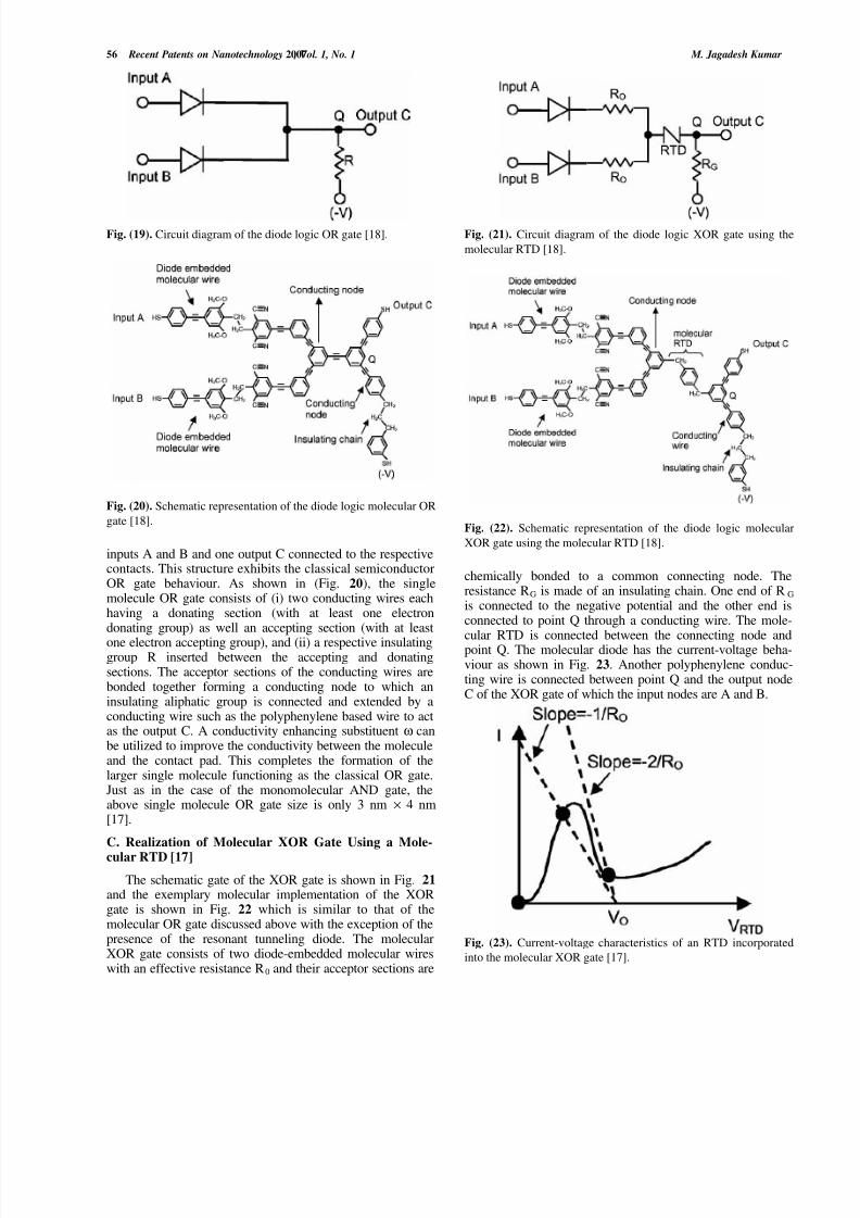
B. Realization of Diode Logic Molecular OR Gate [17]
The circuit representation of a diode logic OR gate isshown in (Fig. 19). The schematic of the exemplary poly-phenylene diode logic molecular OR gate is shown in (Fig.20) and uses the previously discussed rectifying wires as thebuilding blocks. The molecular OR gate consists of two
8/14/2019 Molecular Diodes and Applications
http://slidepdf.com/reader/full/molecular-diodes-and-applications 6/7
56 Recent Patents on Nanotechnology 2007 , Vol. 1, No. 1 M. Jagadesh Kumar
Fig. (19). Circuit diagram of the diode logic OR gate [18].
Fig. (20). Schematic representation of the diode logic molecular OR
gate [18].
inputs A and B and one output C connected to the respectivecontacts. This structure exhibits the classical semiconductorOR gate behaviour. As shown in (Fig. 20), the singlemolecule OR gate consists of (i) two conducting wires eachhaving a donating section (with at least one electrondonating group) as well an accepting section (with at least
one electron accepting group), and (ii) a respective insulatinggroup R inserted between the accepting and donatingsections. The acceptor sections of the conducting wires arebonded together forming a conducting node to which aninsulating aliphatic group is connected and extended by aconducting wire such as the polyphenylene based wire to actas the output C. A conductivity enhancing substituent ω canbe utilized to improve the conductivity between the moleculeand the contact pad. This completes the formation of thelarger single molecule functioning as the classical OR gate.Just as in the case of the monomolecular AND gate, theabove single molecule OR gate size is only 3 nm × 4 nm[17].
C. Realization of Molecular XOR Gate Using a Mole-
cular RTD [17]
The schematic gate of the XOR gate is shown in Fig. 21and the exemplary molecular implementation of the XORgate is shown in Fig. 22 which is similar to that of themolecular OR gate discussed above with the exception of thepresence of the resonant tunneling diode. The molecularXOR gate consists of two diode-embedded molecular wireswith an effective resistance R0 and their acceptor sections are
Fig. (21). Circuit diagram of the diode logic XOR gate using the
molecular RTD [18].
Fig. (22). Schematic representation of the diode logic molecular
XOR gate using the molecular RTD [18].
chemically bonded to a common connecting node. Theresistance RG is made of an insulating chain. One end of R G
is connected to the negative potential and the other end isconnected to point Q through a conducting wire. The mole-
cular RTD is connected between the connecting node andpoint Q. The molecular diode has the current-voltage beha-viour as shown in Fig. 23. Another polyphenylene conduc-ting wire is connected between point Q and the output nodeC of the XOR gate of which the input nodes are A and B.
Fig. (23). Current-voltage characteristics of an RTD incorporated
into the molecular XOR gate [17].

8/14/2019 Molecular Diodes and Applications
http://slidepdf.com/reader/full/molecular-diodes-and-applications 7/7
Molecular Diodes and Applications Recent Patents on Nanotechnology 2007 , Vol. 1, No. 1 57
By combining the above described XOR gate withmolecular AND and OR gates, it is possible to realize morecomplex logic circuits [17,18]. It may be noted that themolecular RTD has two operating points: one on the peak of the RTD operating curve and the second in the valley of theRTD operating curve. The input to the gates will decide inwhich of these two operating points the RTD works. If onlyone of the inputs of the XOR gate is logic 1, the RTD willturn ON forcing the output of the gate to be logic 1. If both
inputs to the XOR gate are logic 1, the RTD is OFF forcingthe output to be logic 0. The presence of RTD and its twooperating points in the I-V curve make the molecular XORgate to behave like the conventional semiconductor XORgate.
CURRENT & FUTURE DEVELOPMENTS
The complete set of single molecule structures (diodes,RTDs, conductors and insulators and the logic gates basedon these) can in fact be used to build more complex Booleanfunctions. For example, by combining the molecular ANDgate and molecular XOR gate, a single molecule HALFADDER can be built. By combining two molecular HALFADDERS, a single molecule FULL ADDER can be built.
Using the above approach, it is also possible to build anelectronic switching device with power gain by adding a gatestructure to a molecular diode forming a single moleculewhich functions as a three terminal transistor similar to the aconventional silicon field effect transistor [18]. As a result, itis now possible to realize in a large single molecule toprovide molecular inverters with power gain, a possibilitywith immense applications in digital circuit design.
REFERENCES
[1] Goldhaber GD, Montemerlo MS, Love JC, Opiteck GJ, EllenbogenJC. Overview of nanoelectronic devices. Proc IEEE 1997; 85: 521-540.
[2] Tour JM, Kozaki M, Seminario JM. Molecular Scale Electronics: ASynthetic/Computational Approach to Digital Computing. J AmChem Soc 1998; 120: 8486- 8493.
[3] Tour JM. Molecular electronics: Synthesis and testing of components. Acc Chem Res 2000; 33: 791-804.
[4] Galatsis K, Wang K, Botros Y, et al. Emerging memory devices -Nontraditional possibilities based on nanomaterials andnanostructures, IEEE Circuits and Devices 2006; 22: 12-21.
[5] Wang D, Heath JR, Sheriff BA. Building ultrahigh-densitynanowire devices: A cross-bar structure approach. Abstr Pap AmChem Soc 2006; 26-INOR: 231.
[6] Heath JR, Ratner MA. Molecular-electronics. Phys Tod 2003; 56:43-49.
[7] Credi A, Balzani V, Langford SJ, Stoddart JF. Logic operations atthe molecular level. An XOR gate based on a molecular machine. JAm Chem Soc 1997; 119: 2679-2681.
[8] Crone B, Dodabalapur A, Lin YY, Filas RW, Bao Z, LaDuca A,Sarpeshkar R, Katz HE, Li W. Large-scale complementaryintegrated circuits based on organic transistors. Nature 2000: 403:521-523.
[9]
Aviram A, Ratner MA. Molecular Rectfiers. Chem Phys Lett 1974;29: 277-283.[10] Collier CP, Wong EW, Belohradsky M, Raymo FM, Stoddart JF,
Kuekes PJ, Williams RS, Heath JR. Electronically configurablemolecular-based logic gates. Science 1999; 285: 391-394.
[11] Kong J, Franklin NR, Zhou CW, Chapline MG, Peng S, Cho KJ,Dai HJ. Nanotube molecular wires as chemical sensors. Science2000; 287 (5453): 622-625.
[12] Bumm LA, Arnold JJ, Cygan MT, Dunbar TD, Burgin TP, Jones L,Allara DL, Tour JM. Weiss PS. Are single molecular wiresconducting? Science 1996; 271 (5256): 1705-1707.
[13] Dekker C. Carbon nanotubes as molecular quantum wires. PhysTod 1999; 52 (5): 22-28.
[14] Magyar RJ, Tretiak S, Gao Y, Wang HL, Shreve AP. A jointtheoretical and experimental study of phenylene-acetylenemolecular wires. Chem Phys Lett 2005; 401 (1-3): 149-156.
[15] Price BK, Tour JM. Functionalization of single-walled carbonnanotubes "on water". J Am Chem Soc 2006; 128 (39): 12899-12904.
[16] De Silva AP, Dixon IM, Gunaratne HQN, Gunnlaugsson T,Maxwell PRS, Rice TE. Integration of logic functions andsequential operation of gates at the molecular-scale. J Am Chem
Soc 1999; 121 (6): 1393-1394.[17] Ellenbogen, J.C.: US20026348700B1 (2002).[18] Ellenbogen, J.C.: US20026339227B1 (2002).[19] Fukuyama H. Physics of molecular conductors. J Phys Soc Japan
2006; 75 (5): Art. No. 051001.[20] Berresheim AJ, Muller M, Mullen K. Polyphenylene nanostruc-
tures. Chem Rev 1999; 99 (7): 1747-1785.[21] Kroto HW, Heath JR, Obrien SC, Curl RF, Smalley RE. C-60 -
Buckminsterfullerene. Nature 1985; 318 (6042): 162-163.[22] James DK, Tour JM. Molecular wires-From design to properties.
Top Curr Chem 2005; 257: 33-62.[23] Avouris P. Molecular electronics with carbon nanotubes. Acc Chem
Res 2002; 35 (12): 1026-1034.[24] Star A, Stoddart JF, Steuerman D. et al, Preparation and properties
of polymer-wrapped single-walled carbon nanotubes. Angew ChemInt Ed 2001; 40 (9): 1721-1725.
[25] McEuen PL, Fuhrer MS, Park H. Single-walled carbon nanotubeelectronics. IEEE Trans Nanotec 2002: 1(3): 78-85.
[26] Naeemi A, Sarvari R, Meindl JD. Performance comparison betweencarbon nanotube and copper interconnects for gigascale integration(GSI). IEEE Electron Device Lett 2005; 26(2) 84-86.
[27] Naeemi A, Meindl JD. Compact physical models for multiwallcarbon-nanotube interconnects. IEEE Electron Device Lett 2006; 27(5): 338-340.
[28] Geddes NJ, Sambles JR, Jarvis DJ, Parker WG, Sandman DJ.Fabrication and investigation of asymmetric current-voltagecharacteristics of a metal langmuir-blodgett monolayer metalstructure. Appl Phys Lett 1990; 56(19): 1916-1918.
[29] Geddes NJ, Sambles JR, Jarvis DJ, Parker WG Sandman DJ. Theelectrical properties of metal-sandwiched langmuir-blodgettmultilayers and monolayers of a redox-active organic molecular-compound. J Appl Phys 1992; 71(2): 756-768.
[30] Brown ER, Soderstrom JR, Parker CD, Mahoney LJ, Molvar KM,Mcgill TC. Oscillations Up To 712 Ghz In Inas/Alsb Resonant-Tunneling Diodes. Appl Phys Lett 1991; 58 (20): 2291-2293.
[31] Sun JP, Haddad GI, Mazumder P, Schulman JN. Resonanttunneling diodes: Models and properties. Proc IEEE 1998; 86 (4):641-661.
[32] Bjork MT, Ohlsson BJ, Thelander C.et al, Nanowire resonanttunneling diodes. Appl Phys Lett 2002; 81(23): 4458-4460.
[33] Mayer TS, Cai LT, Yoon H, et al, Bistable switching in nanoscalemolecular junctions. Abstr Pap Am Chem Soc 2006; 257-Phys:231.
[34] Seminario JM, Zacarias AG, Tour JM. Theoretical study of amolecular resonant tunneling diode. J Am Chem Soc 2000; 122(13): 3015-3020.
[35] Keane ZK, Ciszek JW, Tour JM, Natelson D. Three-terminaldevices to examine single-molecule conductance switching. NanoLett 2006; 6 (7): 1518-1521.
[36] Reed MA, Zhou C, Muller CJ, Burgin TP, Tour JM. Conductanceof a molecular junction. Science 1997; 278 (5336): 252-254.
[37] Zhou C, Deshpande MR, Reed MA, Jones L, Tour JM. Nanoscalemetal self-assembled monolayer metal heterostructures. Appl Phys
Lett 1997; 71 (5): 611-613.[38] Guo XF, Zhang DQ, Zhang GX, Zhu DB. Monomolecular logic:
"Half-adder" based on multistate/multifunctional photochromicspiropyrans. J Phys Chem B 2004; 11942-11945.
[39] Ellenbogen JC, Love JC. Architectures for molecular electroniccomputers: 1. Logic structures and an adder designed frommolecular electronic diodes. Proc IEEE 2000; 88 (3): 386-426.
[40] Gittins DI, Bethell D, Schiffrin DJ, Nichols RJ. A nanometre-scaleelectronic switch consisting of a metal cluster and redox-addressable groups. Nature 2000; 408 (6808): 67-69.