module 5 lecture 1 interfacing serial d a to a micro ... · eel 3923c, fall 2010, t. nishida 2...
TRANSCRIPT

1 EEL 3923C, Fall 2010, T. Nishida
EEL 3923C JD/ Module 5 Microcontroller Applications,
Interfacing a Serial D/A Converter (Lecture 1) Anthony Spears
Fall 2010

2 EEL 3923C, Fall 2010, T. Nishida
Assignment (Serial DAC) A. Design in notebook 1. Design of serial interface between the microcontroller and the DAC 2. Design for a 1kHz triangle wave out. What values will be put in memory? 3. Write pseudo code for a 1kHz triangle wave output from your microcontroller B. Write and compile code for your microcontroller 1. Load and compile sine wave example code for your microcontroller 2. Write and compile your own triangle wave code for your microcontroller C. Build the 2 circuits on the breadboard 1. Hook up microcontroller, DAC and speaker on your breadboard D. Measure/demonstrate in lab 1. 1kHz triangle wave out to speaker 2. View wave on oscilloscope 3. Upload your own code to E-learning which will check for originality. 4. Upload report using template.

3 EEL 3923C, Fall 2010, T. Nishida
Communication Terminology Simplex Communication
Duplex Communication > Half-duplex
> Full-duplex

4 EEL 3923C, Fall 2010, T. Nishida
ASCII Communication Codes ASCII (American Standard Committee for Information Interchange) codes Error Detection Parity bits [Example] A C Parity algorithms 7-bit ASCII 100 0001 100 0011
» Even parity 0100 0001 1100 0011 » Odd parity 1100 0001 0100 0011 » Mark parity 1100 0001 1100 0011 » Space parity 0100 0001 0100 0011

5 EEL 3923C, Fall 2010, T. Nishida
RS232C Interface

6 EEL 3923C, Fall 2010, T. Nishida
Serial Communication Principles
UART (Universal Asynchronous Receiver Transmitter) hardware Serial Errors - Timing errors – i.e. Mismatched baud rates Framing errors – Stop bit not found Overrun errors – Receive character overwritten

7 EEL 3923C, Fall 2010, T. Nishida
SCI Baud Rate Divider Chain
Generic Baud Rate Divisor • D = Divisor = Two Byes • Change D to divide down clk to desired baud rate
Crystal oscillator
Divide by 256
Rate control
(Divide by D)
BRD Reg
Transmit clock
Receive clock
Baud Rate = E-Clock/256 ÷ BRD
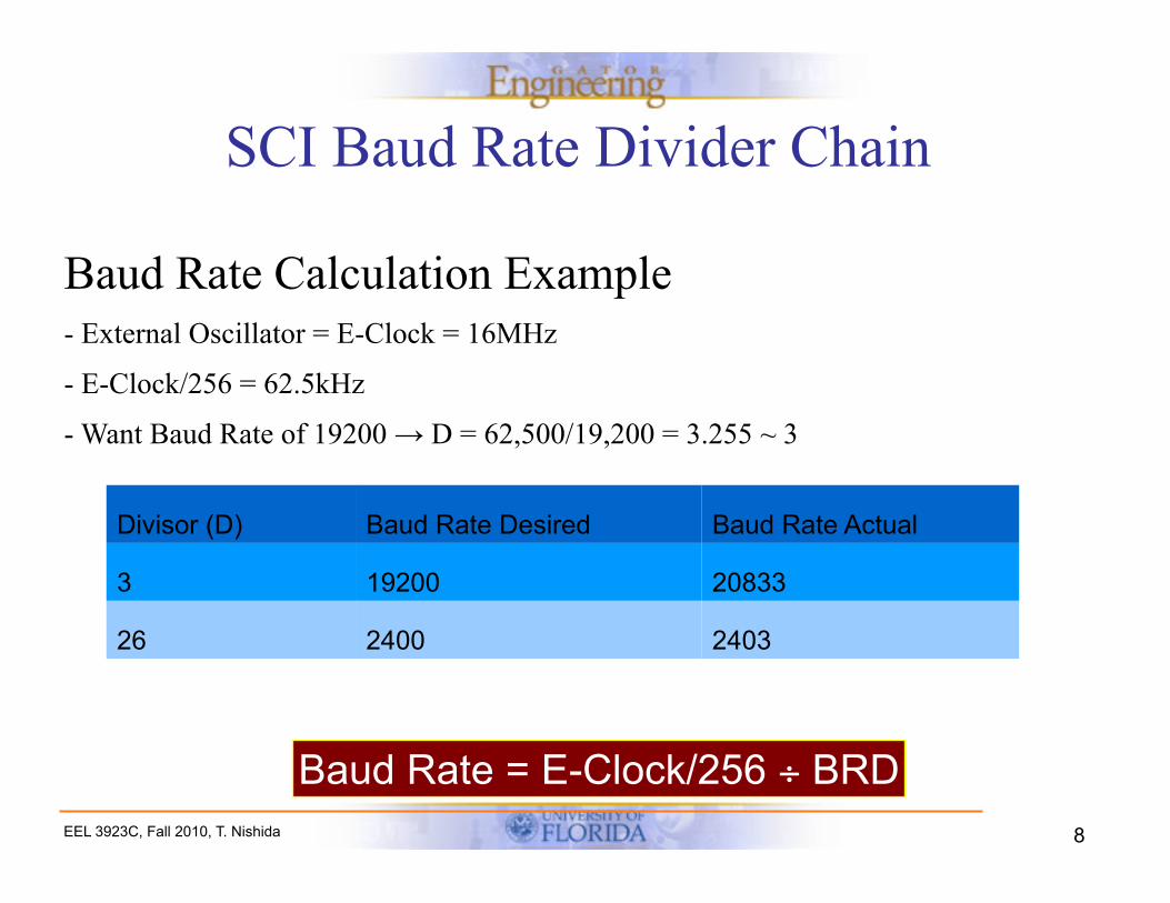
8 EEL 3923C, Fall 2010, T. Nishida
SCI Baud Rate Divider Chain
Baud Rate Calculation Example - External Oscillator = E-Clock = 16MHz
- E-Clock/256 = 62.5kHz
- Want Baud Rate of 19200 → D = 62,500/19,200 = 3.255 ~ 3
Baud Rate = E-Clock/256 ÷ BRD
Divisor (D) Baud Rate Desired Baud Rate Actual
3 19200 20833
26 2400 2403

9 EEL 3923C, Fall 2010, T. Nishida
SCI Baud Rate Registers
Baud Rate = E-Clock/256 ÷ BRD
10 EEL 3923C, Fall 2010, T. Nishida
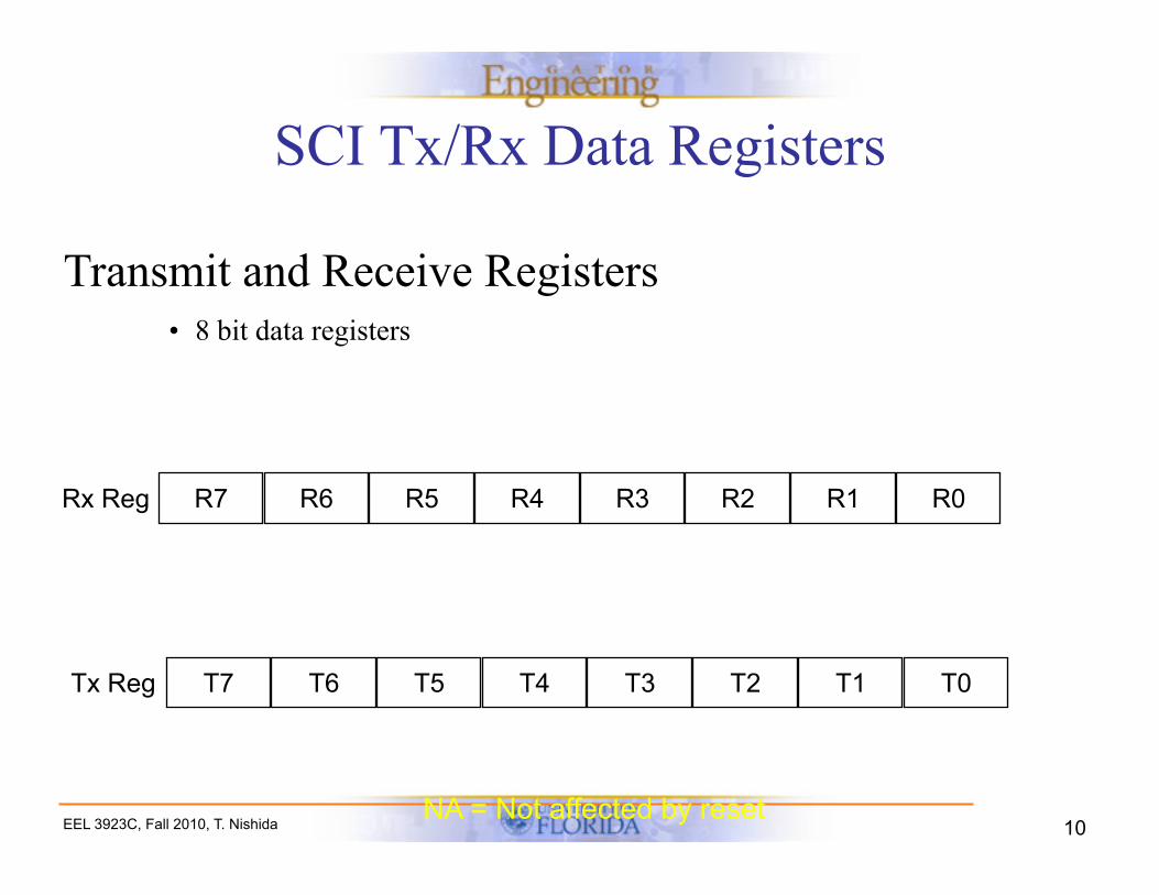
SCI Tx/Rx Data Registers
R7 R6 R5 R4 R3 R2 R1 R0 Rx Reg
NA = Not affected by reset
T7 T6 T5 T4 T3 T2 T1 T0 Tx Reg
Transmit and Receive Registers • 8 bit data registers

11 EEL 3923C, Fall 2010, T. Nishida
UART Control Registers

12 EEL 3923C, Fall 2010, T. Nishida
UART Flags and Interrupts • Interrupts enabled through control registers • Flags read from status or control registers • Receive Flag/Interrupt means new data was received in the
buffer and is ready to be read • Transmit Flag/Interrupt means buffer is empty and ready to
send new data
13 EEL 3923C, Fall 2010, T. Nishida
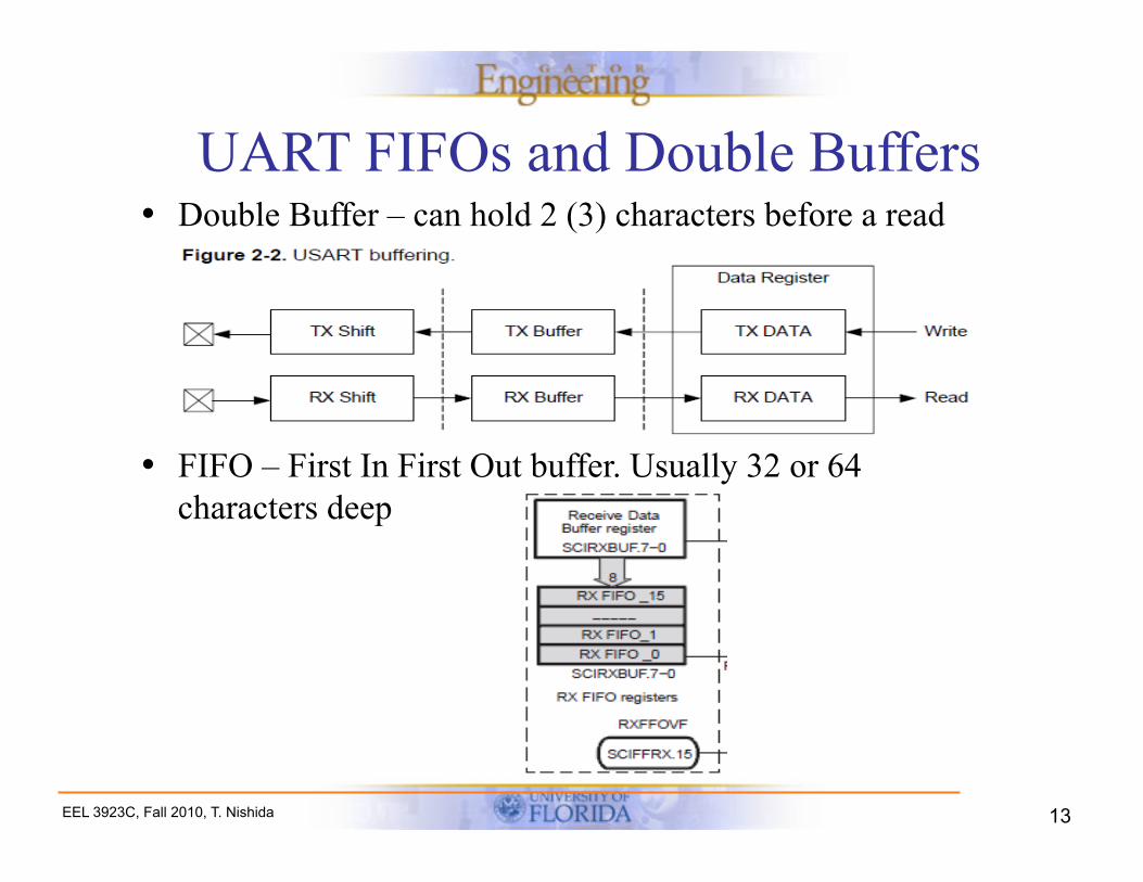
UART FIFOs and Double Buffers • Double Buffer – can hold 2 (3) characters before a read
• FIFO – First In First Out buffer. Usually 32 or 64 characters deep

14 EEL 3923C, Fall 2010, T. Nishida
SPI • SPI – Serial Peripheral Interface • Full Duplex • Master has control of the communication: sends Clock and
Select signals to the Slave • Slave sends data through MISO and Master sends data out
through MOSI

15 EEL 3923C, Fall 2010, T. Nishida
SPI – SCK (Clock from Master), MISO (Master In Slave Out
data), MOSI (Master Out Slave In data), /SS (Slave Chip Select signal from Master)

16 EEL 3923C, Fall 2010, T. Nishida
SPI – Communication is controlled by Master
• Master sends CLK and /SS to Slave – Example
• Master sets Slave Select signal low • Master sends CLK and Address of data in Slave (MOSI) • Master sends CLK and Slave sends Data (MISO) • Master sets Slave Select signal high
– Both Master and Slave can TX and RX data at the same time – Uses:
• Sensors, Control Devices, Communications, External Memory (Flash, EEPROM...), LCD Displays, SD/MMC cards, Between Microcontrollers

17 EEL 3923C, Fall 2010, T. Nishida
I2C – Half Duplex – Only 1 Data Line – I2C Signals: SCL (Serial Clock), SDA (Serial Data) – 2 Open Drain Lines – need pullup resistors – 1 Master – multiple slaves on same lines

18 EEL 3923C, Fall 2010, T. Nishida
I2C – Master initiates data transfer with a Start Condition – Master sends Slave I2C address – Master sends R/W to either read from or write to Slave – Slave Sends ACK bit then Data – Master Sends ACK bit – Ends with Master sending the Stop Condition
– Only one Master or Slave can have control of bus at once – I2C Address – 7 bits
• Used to identify which slave to communicate with on a shared bus

19 EEL 3923C, Fall 2010, T. Nishida
I2C - I2C timing example

20 EEL 3923C, Fall 2010, T. Nishida
Bit Banging – Implement serial protocols such as I2C and SPI
with software instead of dedicated hardware – Manually set each data bit, set the enable, and
toggle the clock by writing a 1 or 0 to dedicated pins for each signal (EN, CLK, DATA)
– Less efficient than using the dedicated hardware but allows for the simple implementation of serial protocols without hardware changes
– Can use any general input/output pin for each signal

21 EEL 3923C, Fall 2010, T. Nishida
Bit Banging
void dac_write(char data){
unsigned int output = 0x0000;
unsigned char temp;
signed char x;
TRISDbits.TRISD0 = 0; // set direction register
TRISDbits.TRISD1 = 0;
TRISDbits.TRISD2 = 0;
PORTDbits.RD0 = 0; // data to 0
PORTDbits.RD1 = 0; // clock to 0
PORTDbits.RD2 = 1; // enable to 1
PORTDbits.RD2 = 0; //enable low
for (x = 15; x > -1; x--){ // send 16 bits of data
PORTDbits.RD0 = (output >> x) & 0x01;
PORTDbits.RD1 = 1;
PORTDbits.RD1 = 0;
PORTDbits.RD0 = 0;
}
PORTDbits.RD2 = 1; //enable high
}
– Procedure: • Enable = True • Loop for Each Bit: output data bit, clock high, clock low • Enable = False

22 EEL 3923C, Fall 2010, T. Nishida
EEL 3923C JD/ Module 5 Microcontroller Applications,
Interfacing a Serial D/A Converter (Lecture 2 Examples)
Anthony Spears Fall 2010

23 EEL 3923C, Fall 2010, T. Nishida
Assignment (Serial DAC) A. Design in notebook 1. Design of serial interface between the microcontroller and the DAC 2. Design for a 1kHz triangle wave out. What values will be put in memory? 3. Write pseudo code for a 1kHz triangle wave output from your microcontroller B. Write and compile code for your microcontroller 1. Load and compile sine wave example code for your microcontroller 2. Write and compile your own triangle wave code for your microcontroller C. Build the 2 circuits on the breadboard 1. Hook up microcontroller, DAC and speaker on your breadboard D. Measure/demonstrate in lab 1. 1kHz triangle wave out to speaker 2. View wave on oscilloscope 3. Upload your own code to E-learning which will check for originality. 4. Upload report using template.

24 EEL 3923C, Fall 2010, T. Nishida
MSP430 DAC Connections

25 EEL 3923C, Fall 2010, T. Nishida
AVR DAC Connections
26 EEL 3923C, Fall 2010, T. Nishida
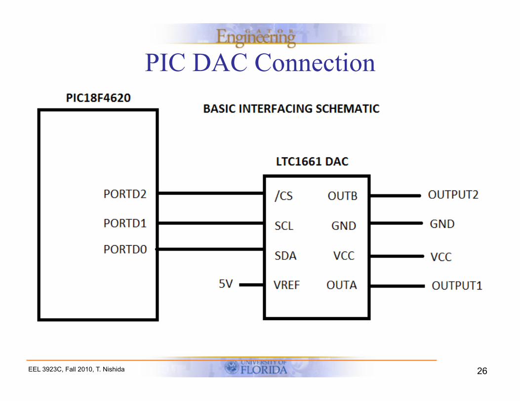
PIC DAC Connection

27 EEL 3923C, Fall 2010, T. Nishida
DAC Sine Wave Example