modified bridgeless rectifier for pfc with minimized stress · modified bridgeless rectifier for...
TRANSCRIPT
72
Journal of Engineering Technology (ISSN: 0747-9964) Volume 6, Issue 1, Jan, 2017, PP.72-89
Modified Bridgeless Rectifier for PFC with Minimized Stress
*1Vinaya Sagar Kommukuri,
2Kanungo Barada Mohanty,
3Kishor Thakre,
4Aditi Chatterjee,
5Ashwini Kumar Nayak
12345Department of Electrical Engineering National Institute of Technology Rourkela, Rourkela,
Odisha 769008, India
Abstract. A high performance single phase modified bridgeless ac-dc converter with an automatic
power factor correction is introduced. The proposed converter is based on a single ended primary
inductance converter (SEPIC) topology and operated in continuous conduction mode (CCM) to meet
the demands of power factor correction (PFC) to unity and output voltage regulation. It offers many
advantages, such as fewer semiconductor devices, low stress on each component, improved efficiency,
high power factor compared to classical converter .Detailed analysis of the converter is presented.
Simulation and experimental results are discussed for a 300W prototype to verify the performance of
the converter.
Keywords: Power factor correction (PFC); continuous conduction mode (CCM); single ended
primary inductance converter (SEPIC).
1. Introduction
Many applications like computers, telecom equipment, biomedical industries and LED lighting uses
AC-DC conversion which involves conventional bridge rectifier with large capacitor at output end is
unavoidable, results in low power factor of about 0.5-0.7[1]. As per the Stringent international
standards like International Electronic Commission (IEC) 6100-3-2, harmonics produced by the
electronic equipment like rectifiers should be limited [2].Therefore, the power factor improvement is
mandatory for single phase power supplies to meet the demands like reduction of current harmonics
and power factor correction (PFC).The most conventional PFC converter is a bridge rectifier
followed by a DC-DC converter. Boost converter is widely used as the DC-DC converter in PFC
circuits because of its simplicity, low cost and high performance though it is having output voltage
greater than the peak input voltage.
In large no of applications, it is preferred to have the PFC output voltage lower than the input ac
voltage, a buck type converter is recommended. The input current of buck converter is discontinuous
and to shape it like sinusoidal another passive filter must be used at the input side of the buck
converter. This is the characteristics of all converters in which a buck converter is at its input, such as
buck-boost, noninverting buck-boost, flyback etc.,[ 3-5]. On the other side, a SEPIC converter can
provide a high power actor regardless of its output voltage due to its step up/down function.
However, all the above addressed conventional PFC rectifiers includes a front end bridge rectifier
which leads to high conduction losses, resulting in additional thermal management and decrease the
efficiency of the PFC converter. In order to enhance the efficiency of the conventional PFC

73
Journal of Engineering Technology (ISSN: 0747-9964) Volume 6, Issue 1, Jan, 2017, PP.72-89
converters bridgeless PFC converters have been proposed such as buck, buck-boost, boost, sepic [6-
17].Since Bridgeless PFC rectifiers has lower no of semiconductor devices in the current path ,results
in lower conduction losses ,higher efficiency and cost saving.
The bridgeless PFC boost rectifier is predominant because of its simplicity but it has same major
practical drawbacks like difficulty in providing input-output isolation, high startup inrush current and
lack of current limiting during overload conditions as in conventional boost PFC converter. Therefore
research has been focused on bridgeless sepic PFC since it is a solution for many applications.
Recently many bridgeless SEPIC PFC converters have been proposed in the literature. Bridgeless
SEPIC PFC circuits that are proposed in the literature [18-23], operates under DCM mode suffers
with high voltage and current stress that highly degrades the performance of the converter and limits
its application range.
To overcome aforementioned defects, a modified bridgeless SEPIC PFC with continuous conduction
mode (CCM) with reduced stress is presented. This meets the challenges of near unity power factor
and output voltage regulation. The remaining sections of the paper is organized as follows. Principle
of operation is discussed in section 2. In section 3 theoretical analysis are design procedure and
experimental considerations are given. Efficiency improvement is explained in section 4. The
simulation results are presented in section 5. Experimental results and conclusion are given in section
6 and 7, respectively.
2. Operation of Bridgeless SEPIC converter in CCM mode
The circuit diagram of conventional SEPIC PFC rectifier and modified Bridgeless SEPIC are shown
in Fig.1 and Fig.2. Bridgeless SEPIC is combination of both bridge rectifier and classical SEPIC
converter, so it is known as Bridgeless SEPIC converter. It is having fewer semiconductor
components. Operation of the circuit is similar to classical sepic converter and is symmetrical in two
half –line cycles of input voltage. Thus, the operation of the converter is considered during one
switching period in the positive half –line cycle of the input voltage. The converter is operated in
CCM mode i.e., output diode turns off when the switch is turned on. The capacitance of the output
capacitor Co is adequately high enough to make it ideal dc voltage source as shown in Fig.2.Also, the
supply voltage is assumed constant and equal to Vin in a switching period Ts.
To simplify the analysis, it is assumed that the converter is operating at steady state and all
components are ideal. The circuit operation in a switching cycle is divided into two modes.Fig.3 and
Fig.4 shows the schematic diagram of mode I and mode II in the positive half cycle. The theoretical
waveforms of the converter are shown in Fig.5.
Vin
Cc
C0S1
L1
L2
D0
Fig 1. Conventional SEPIC PFC rectifier

74
Journal of Engineering Technology (ISSN: 0747-9964) Volume 6, Issue 1, Jan, 2017, PP.72-89
Vin
D1
Cc
S1
S2
L1
L2
D2
D0
C0
Cm
D3
Fig 2. Modified Bridgeless SEPIC PFC rectifier
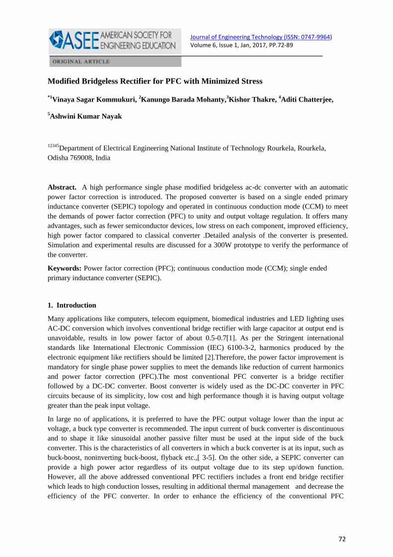
Mode I (t0-t1):
At t0, both switches S1, S2 and diode D1 are in ON state and output diode D0 is in OFF state.
Capacitors CC and Cm follows the input voltage. The load current is provided by the output capacitor
as the output diode is reverse biased. Here the switch current is combination of currents flowing
through inductors L1 and L2.Input inductor current iL1 starts to increase linearly by a slope of Vin (t0)/
L1 and output inductor current iL2 starts decreasing linearly by the slope of (VCc –VCm)t0/ L2.This mode
ends by turning off the switches S1 and S2.Switch current is given by the equation (1).
tL
tV
L
tViiI inin
LLtS
2
0
1
0
211
)()( (1)
where )( 0
1
1 ttL
Vi in
L
(2)
)( 0
2
2 ttL
VVi CmCc
L
= )( 0
2
ttL
Vin
(3)
inCmCc VVV (4)
Vin
D1
Cc
S1
S2
L1
L2
D2
D0
C0
Cm
D3
Fig 3. Mode I

75
Journal of Engineering Technology (ISSN: 0747-9964) Volume 6, Issue 1, Jan, 2017, PP.72-89
Mode II (t1-t2):
At t1, switches S1 and S2 are turned off and diodes D3 and D0 starts conducting. The voltage
across switches begins to increase. Energy stored in the input inductor is transferred to the output
through the coupling capacitor Cc1 and output diode D0 and also to the Cc2 through diode D3 at the
same time .Energy stored in inductor L2 is transferred to the output through diode D0.This mode ends
by starting the next switching cycle at t2.
1
1
111 ttL
VVtii CmCc
LL
(5)
1
2
122 ttL
Vtii Cc
LL
(6)
CmCc VVV 0 (7)
Vin
D1
Cc
S1
S2
L1
L2
D2
D0
C0
Cm
D3
Fig 4. Mode II
76
Journal of Engineering Technology (ISSN: 0747-9964) Volume 6, Issue 1, Jan, 2017, PP.72-89
Pulses
S1,S2
IS1
VS1
ID0,ID3
VD0
IL1
IL2
t0 t1 t2
(Vin+V0)/2
DIL
(Vin+V0)/2
IS1/2
Fig 5. Theoretical waveforms of the Converter
3. Theoretical Analysis
3.1 Static gain:
The average inductor voltage at steady state is considered to be zero. By applying volt-second balance
to the inductor 1L is given by equation (8)

77
Journal of Engineering Technology (ISSN: 0747-9964) Volume 6, Issue 1, Jan, 2017, PP.72-89
oncminonin tTVVtV (8)
From equation (4) & (7) we get
2
0 in
cm
VVV
(9)
From equation (8) & (9) we get
in
inon
VV
VV
T
tD
0
0 (10)
Now, static gain is given by equation (11)
D
D
V
V
in
1
10 (11)
3.2 Inductors L1 and L2:
Inductors L1 and L2 are calculated as a specification of maximum input current ripple LiD .The peak
input current is calculated by equation (12) assuming the current ripple given by equation (13).The
inductors L1 and L2 are given by equation (14)
)sin(2
)(
0)( t
V
PI
rmsin
peakin
(12)
s
in
LLf
DVi D (13)
sL
in
fi
DVLL
D 21 (15)
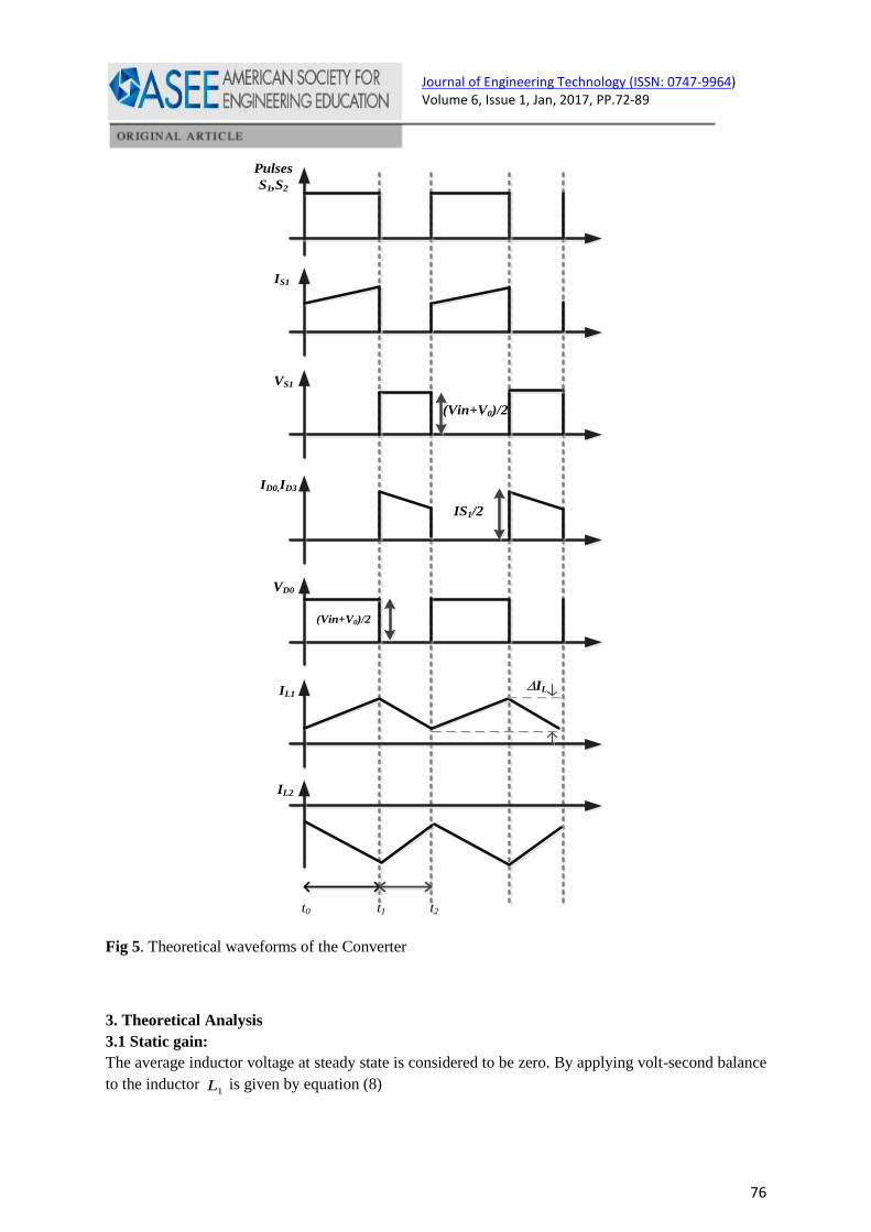
3.3 Capacitors CC and Cm
It has a considerable impact in the input current waveform since the capacitors cC and
mC
follows the input line voltage within line period and is constant in one switching period. Resonant
frequency rf plays a vital role in the design of capacitor cC and
mC . The resonant frequency rf
of coupling capacitorcC and
mC , inductor (L1) and inductor (L2) should be greater than line frequency
lf to avoid the input current oscillations at each half line cycle, likewise resonant frequency rf
should be lower than the switching frequency sf to make sure that the capacitor voltage is constant
in a switching time sT .Accordingly cC and
mC can be obtained from the following equation.
78
Journal of Engineering Technology (ISSN: 0747-9964) Volume 6, Issue 1, Jan, 2017, PP.72-89
21
24
1
LLfCC
r
Cm
(16)
Where srl fff
rf value is chosen as 5 kHz to meet the requirement.
45 90 135 1800
50
100
150
200
250
300 Output voltage of the converter (V0)
Switch voltage of the converter
ωt
0
V
CcV
CmV
CmCco VVV
Fig 6. Theoretical waveforms of the Capacitor voltages
The voltage across the capacitors cC and
mC are given by the equation (17) and (18) and are shown in
Fig .6.
DVV inCc
1
1 (17)
D
DVV inCm
1 (18)
3.4 Output Capacitor 0C
Since output voltage ripple is two times the input line frequency, output capacitor must be large
enough to reduce the output voltage ripple0VD .Therefore, output capacitor voltage is obtained from
the following equation
00
0
04 VVf
PC
l D (19)
79
Journal of Engineering Technology (ISSN: 0747-9964) Volume 6, Issue 1, Jan, 2017, PP.72-89
where lf is input line frequency and 0VD is output voltage ripple.
3.5 Maximum voltage and current rating of switching devices
The maximum switch voltage and current of the converter is obtained from the following equation.
2
0(min)
(min)2,1
VVV
in
S
(20)
2
0(max)
(max)2,1
VVV
in
S
(21)
0(min)min1 IIII LinS D (22)
0(max)max1 IIII LinS D (23)
3.6 Controller Design
The average current mode control is used to generate the current reference for the bridgeless
SEPIC converter. The design of the converter is done based on CCM mode. The converter uses
UC3854 as a controller, which gives current shape and frequency that follows line current using
synchronous feedback loop [ 25].
To get near unity power factor, the controller needs voltage and current feedback signals are
sensed from the converter. In the given circuit input voltage is sensed from capacitors cC and
mC
since they follows the input voltage, Input inductor current signal is sensed from diode currents (ID1
and ID2) as shown in Fig.7. Then the reference current is computed by a multiplier of the
synchronous feedback loop, output voltage feedback loop, and input voltage feed forward loop. The
control circuit of the converter is shown in Fig.7. The voltage feedback loop should have a very low
bandwidth, well below the line frequency, in order to minimize input current distortion [26,27].
AdderAdder
Voltage
error
Amplifier
Voltage
error
AmplifierVRef
MultiplierMultiplier
Current
error
Amplifier
Current
error
Amplifier
+_
VCc+VCm
ID1
V0
ID2
fs=100 Khz
S1,S2
1/k1/k
Fig 7. Block diagram for Controller
80
Journal of Engineering Technology (ISSN: 0747-9964) Volume 6, Issue 1, Jan, 2017, PP.72-89
4. Efficiency improvement
Based on the number of components present in the converter, the efficiency enhancement of
the converter is analyzed. From the operation of the converter, it is seen that a diode in the rectifier is
removed and the other diode is substituted by a switch. Assuming the forward voltage drop of the
diodes in the converter is 1V and the voltage drop of the power MOSFET is negligible since RDS(on) is
small. The theoretical calculations of the power dissipation of the reduced components is given by
(24).
WdtIVT
P
T
DDavgD 15.31
0
, (24)
Where T= π, VD= 1V, ID=4.991sin (ω) and avgDP , is average power loss in one diode of
the input rectifier. The efficiency improvement of 300W converter is calculated by (25).
%11.2300
2 ,
avgD
timprovemen
P (25)
In general the efficiency enhancement is less than 2.11% due to the assumption of the zero
voltage drop of switch.
5. Simulation results
The proposed converter is simulated in LT Spice IV. Specifications and parameters of the
converter are as follows: Vin = 85 VRms, V0 = 250 Vdc, ∆iL1 = 20% of iL1, sf = 100 kHz and P0 = 300
W. According to the design considerations, the circuit elements are obtained as L1=L2= 2mH, Cc=
0.62µF, and C0= 1200µF.
To achieve PFC and regulated output voltage average current mode control is used. It
includes an inner current loop and outer voltage loop. Here capacitor voltages are sensed since they
follows input voltage which is given to one of the multiplier input. The output voltage is sensed and
processed through voltage error amplifier which feeds the other input port of the multiplier. The
output of the multiplier generates current reference which is compared with input current that is
sensed from sum of the diode current. The output of the current error signal is compared with ramp
signal to generate gate pulses.
The input voltage and current waveforms in simulation are shown in Fig. 8 (a). It is observed
that both are in phase which depicts the property of power factor correction of the converter. Fig .8 (b)
illustrates the output voltage and output current waveforms respectively. The capacitor voltage
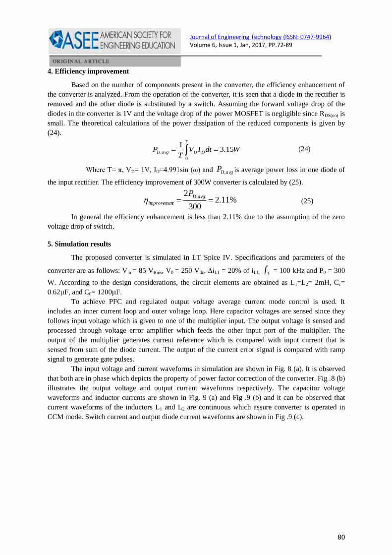
waveforms and inductor currents are shown in Fig. 9 (a) and Fig .9 (b) and it can be observed that
current waveforms of the inductors L1 and L2 are continuous which assure converter is operated in
CCM mode. Switch current and output diode current waveforms are shown in Fig .9 (c).

81
Journal of Engineering Technology (ISSN: 0747-9964) Volume 6, Issue 1, Jan, 2017, PP.72-89
(a)
(b)
Fig 8. (a) Input voltage and current waveforms (b) Output voltage and current waveforms
(a)
82
Journal of Engineering Technology (ISSN: 0747-9964) Volume 6, Issue 1, Jan, 2017, PP.72-89
(b)
(c)
Fig 9. (a).Capacitor voltage waveforms (b). Inductor current waveforms (c).Switch and Diode current
waveforms
6. Experimental results
The theoretical analysis of the proposed converter is validated by experimental prototype with
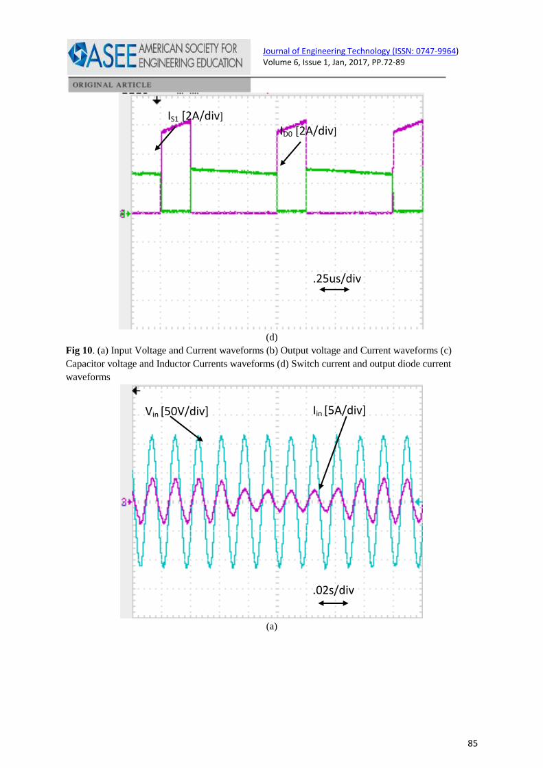
the same specifications of the modified bridgeless SEPIC PFC converter. Fig. 10(a) presents the
experimental results of the input current and input voltage. It is noticed that the measured power
factor is near to unity, since voltage and current waveforms are in phase. Output voltage and output
current of the converter are shown in Fig. 10(b). Capacitor voltage and inductor current (IL1) and (IL2)
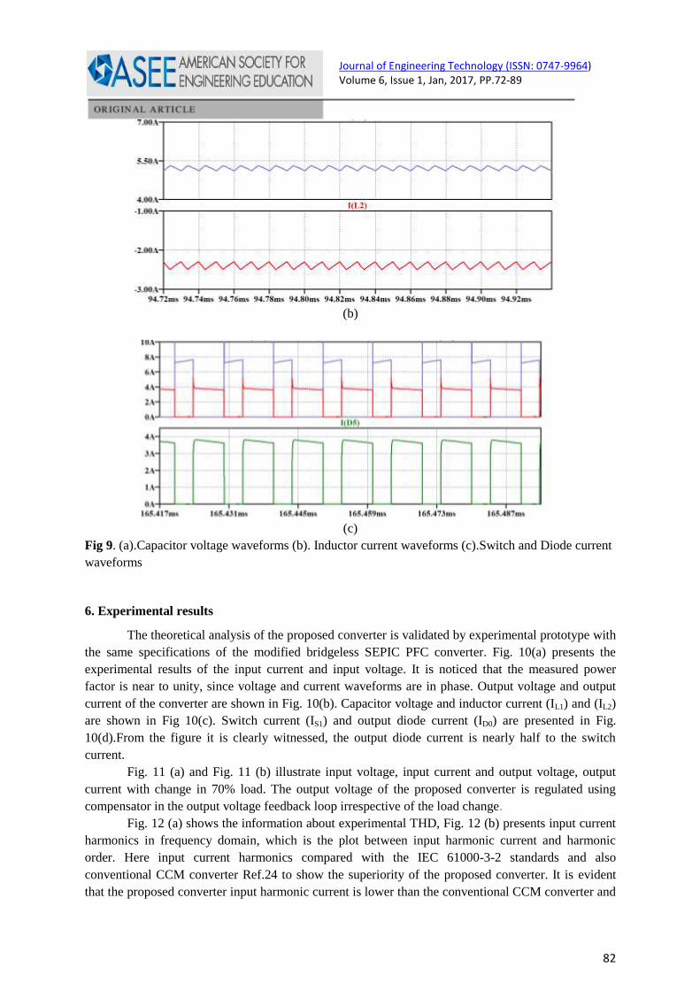
are shown in Fig 10(c). Switch current (IS1) and output diode current (ID0) are presented in Fig.
10(d).From the figure it is clearly witnessed, the output diode current is nearly half to the switch
current.
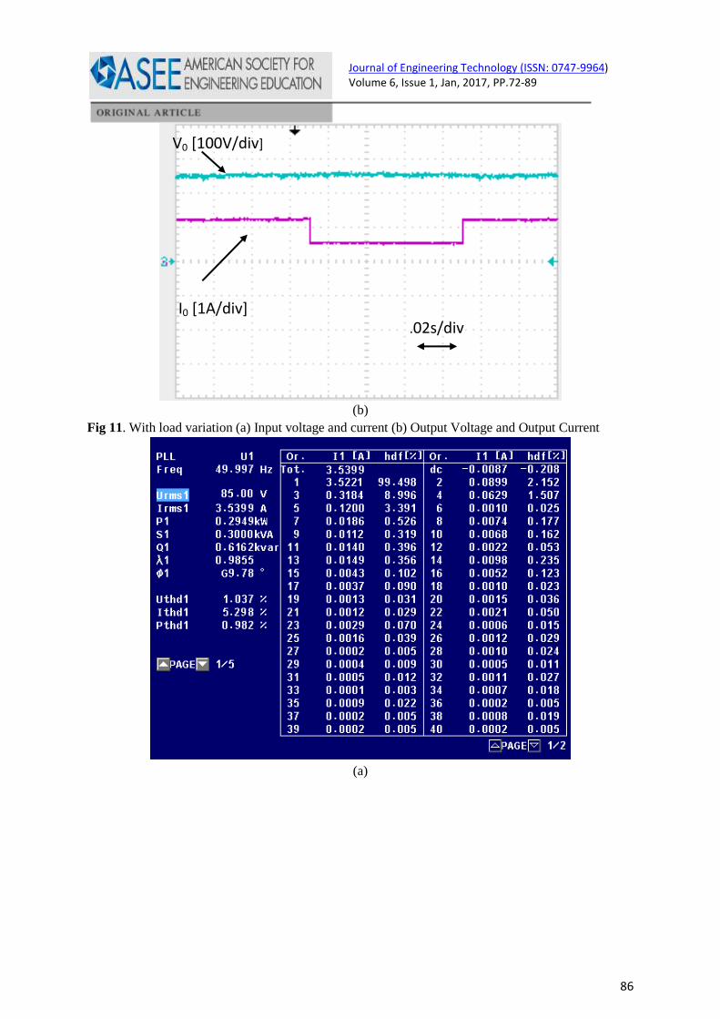
Fig. 11 (a) and Fig. 11 (b) illustrate input voltage, input current and output voltage, output
current with change in 70% load. The output voltage of the proposed converter is regulated using
compensator in the output voltage feedback loop irrespective of the load change.
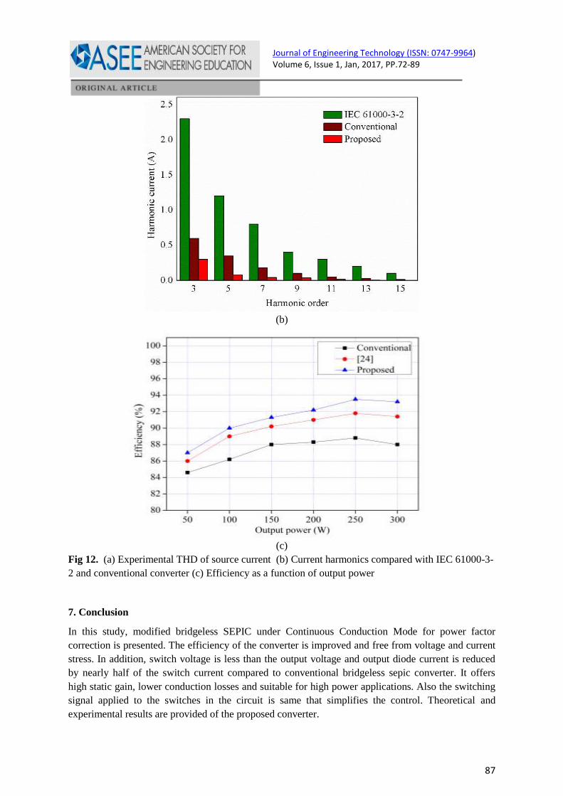
Fig. 12 (a) shows the information about experimental THD, Fig. 12 (b) presents input current
harmonics in frequency domain, which is the plot between input harmonic current and harmonic
order. Here input current harmonics compared with the IEC 61000-3-2 standards and also
conventional CCM converter Ref.24 to show the superiority of the proposed converter. It is evident
that the proposed converter input harmonic current is lower than the conventional CCM converter and

83
Journal of Engineering Technology (ISSN: 0747-9964) Volume 6, Issue 1, Jan, 2017, PP.72-89
follows the IEC 61000-3-2 standards. Fig.12 (c) shows the efficiency of the proposed converter as a
function of output power in comparison with conventional and contemporary topology Ref.24. It
depicts that the proposed converter shows the superior performance than the other converters at
various output power.
(a)
(b)
Vin [50V/div] Iin [4A/div]
V0 [100V/div]
I0 [1A/div]
.01s/div
.01s/div

84
Journal of Engineering Technology (ISSN: 0747-9964) Volume 6, Issue 1, Jan, 2017, PP.72-89
(c)
VCc [100V/div]
IL1 [2A/div]
.25us/div
.005s/div
VCm [100V/div]
IL2 [1A/div]
85
Journal of Engineering Technology (ISSN: 0747-9964) Volume 6, Issue 1, Jan, 2017, PP.72-89
(d)
Fig 10. (a) Input Voltage and Current waveforms (b) Output voltage and Current waveforms (c)
Capacitor voltage and Inductor Currents waveforms (d) Switch current and output diode current
waveforms
(a)
Vin [50V/div] Iin [5A/div]
.02s/div
.25us/div
IS1 [2A/div]
ID0 [2A/div]
86
Journal of Engineering Technology (ISSN: 0747-9964) Volume 6, Issue 1, Jan, 2017, PP.72-89
(b)
Fig 11. With load variation (a) Input voltage and current (b) Output Voltage and Output Current
(a)
V0 [100V/div]
I0 [1A/div]
.02s/div
87
Journal of Engineering Technology (ISSN: 0747-9964) Volume 6, Issue 1, Jan, 2017, PP.72-89
(b)
(c)
Fig 12. (a) Experimental THD of source current (b) Current harmonics compared with IEC 61000-3-
2 and conventional converter (c) Efficiency as a function of output power
7. Conclusion
In this study, modified bridgeless SEPIC under Continuous Conduction Mode for power factor
correction is presented. The efficiency of the converter is improved and free from voltage and current
stress. In addition, switch voltage is less than the output voltage and output diode current is reduced
by nearly half of the switch current compared to conventional bridgeless sepic converter. It offers
high static gain, lower conduction losses and suitable for high power applications. Also the switching
signal applied to the switches in the circuit is same that simplifies the control. Theoretical and
experimental results are provided of the proposed converter.

88
Journal of Engineering Technology (ISSN: 0747-9964) Volume 6, Issue 1, Jan, 2017, PP.72-89
References
[1]. C.M. Wang, A novel zero-voltage-switching PWM boost rectifier with high power factor and
low conduction losses, IEEE Transactions. Ind. Electron, 52 (2005) 427–435.
[2]. IEC 61000-3-2, International Electro technical Commission Genève, Switzerland, 1998
[3]. R. Itoh et. al., Single-phase buck rectifier employing voltage reversal circuit for sinusoidal input
current wave shaping, IEE Proc. Electr. Power Appl., 146 (1999) 707–712.
[4]. R. Oruganti et. al., Inductor voltage control of buck-type single-phase ac-dc converter, IEEE
Trans. Power Electron, 15 (2000) 411–416.
[5]. M. A. Al-Saffar et. al., Integrated buck–boost–quadratic buck PFC rectifier for universal input
applications, IEEE Trans. Power Electronics, 24 (2009) 2886-2896.
[6]. W. Wei et. al., A novel bridgeless buck-boost PFC converter, IEEE power electronics specialists
conference, (PESC) 2008, pp. 1304-08.
[7]. K. Mok et. al., A single-stage bridgeless power factor correction rectifier based on fly back
topology, IEEE international telecommunications energy conference, (INTELEC) 2011, pp. 1-6.
[8]. Y. Jang et. al., Bridgeless high-power-factor buck converter state-of-the-art, IEEE Trans Ind.
Electron, 26 (2011) 602-611.
[9]. L. Huber et. al., Performance evaluation of bridgeless PFC boost rectifiers, IEEE Trans Power
Electron, 23 (2008)1381-1390.
[10]. W-Y. Choi et. al., Bridgeless boost rectifier with low conduction losses and reduced diode
reverse-recovery problems, IEEE Trans Ind. Electron., 54 (2007) 769-80.
[11]. E. H. Ismail, Bridgeless SEPIC rectifier with unity power factor and reduced conduction losses,
IEEE Trans Ind. Electron, 56 (2009)1147-57.
[12]. K.S. Muhammad et. al., ZCS Bridgeless Boost PFC Rectifier Using Only Two Active Switches,
IEEE Trans. Ind. Electron, 62 (2015) 2795-2806.
[13]. A.A. Fardoun et. al., Bridgeless resonant pseudo boost PFC rectifier, IEEE Trans. Power
Electron, 29 (2014) 5949-5960.
[14]. A. Bouafassa et. al., Design and real time implementation of single phase boost power factor
correction converter, ISA Transactions, 55 (2015) 267–274.
[15]. M. Mahdavi et. al., Zero-current-transition bridgeless PFC without extra voltage and current
stress, IEEE Trans. Ind. Electron, 56 (2009) 2540–2547.
[16]. M. Mahdavi et. al., A new zero voltage transition bridgeless PFC with reduced conduction
losses, Jour. of Power Electron, 9 (2009) 708–717.
[17]. M. Mahdavi et. al., A new soft switching bridgeless PFC without any extra switch, Int. Review.
Electr. Engg, 3 (2008) 858–863.
[18]. A. Sabzali et. al., New bridgeless PFC Sepic and Cuk rectifiers with low conduction and
switching losses, IEEE PEDS, pp. 873–881, 2009.
[19]. M.R. Sahid et. al., A New AC-DC converter using bridgeless SEPIC, IEEE Annual Conf.
Industrial Electronics Society (IECON 2010), pp. 286–290, November 2010.
[20]. A. J. Sabzali et. al., New bridgeless DCM SEPIC and Cuk PFC rectifiers with low conduction
and switching losses, IEEE Trans. Ind. Appl., 47 (2011) 873-81.
[21]. M. Mahdavi et. al., Bridgeless SEPIC PFC rectifier with reduced components and conduction
losses, IEEE Trans Ind. Electron, 58 (2011) 4153-4160.

89
Journal of Engineering Technology (ISSN: 0747-9964) Volume 6, Issue 1, Jan, 2017, PP.72-89
[22]. Jae-won Yang et. al., Bridgeless SEPIC Converter with a Ripple –Free Input Current, IEEE
Trans. Power Electron, 28 (2013) 3388-3394.
[23]. C. G. Bianchin et. al., High-Power-Factor Rectifier Using the Modified SEPIC Converter
Operating in Discontinuous Conduction Mode, IEEE Transactions on Power Electronics, 30
(2015) 4349-4364.
[24]. J.M. Kwon et. al., Continuous-conduction-mode SEPIC converter with low reverse-recovery loss
for power factor correction, IEE Proc. Electr. Power Appl, 153 (2006) 673-681.
[25]. C.S. Silva, Power factor correction with the UC3854, Unitrode Product and Applications
Handbook. (1995–96).
[26]. L. Dixon, High. Power factor pre-regulator using the SEPIC converter, Unitrode Product and
Applications Handbook. (1995–96).
[27]. L.H.Dixon, Control loop design, SEPIC preregulator Example, Unitrode Product and
Applications Handbook. (1993).