modelling and simulation of surface plasmonic resonance...
TRANSCRIPT

MODELLING AND SIMULATION OF SURFACE
PLASMONIC RESONANCE IN PHOTONIC CRYSTAL
FIBER
RIFAT AHMMED AONI
FACULTY OF ENGINEERING
UNIVERSITY OF MALAYA
KUALA LUMPUR
2015

MODELLING AND SIMULATION OF SURFACE
PLASMONIC RESONANCE IN PHOTONIC CRYSTAL
FIBER
RIFAT AHMMED AONI
DESSERTATION SUBMITTED IN FULFILMENT OF
THE REQUIREMENTS FOR THE DEGREE OF MASTER
OF ENGINEERING SCIENCE
FACULTY OF ENGINEERING
UNIVERSITY OF MALAYA
KUALA LUMPUR
2015

iii
UNIVERSITY OF MALAYA
ORIGINAL LITERARY WORK DECLARATION
Name of Candidate: RIFAT AHMMED AONI
Passport No:
Registration/Matric No:
Name of Degree:
KGA130045
Master of Engineering Science
Title of Dissertation (“this Work”):
Modelling and Simulation of Surface Plasmonic Resonance in
Photonic Crystal Fiber
Field of Study: Photonic
I do solemnly and sincerely declare that:
(1) I am the sole author/writer of this Work;
(2) This Work is original;
(3) Any use of any work in which copyright exists was done by way of fair dealing
and for permitted purposes and any excerpt or extract from, or reference to or
reproduction of any copyright work has been disclosed expressly and
sufficiently and the title of the Work and its authorship have been
acknowledged in this Work;
(4) I do not have any actual knowledge nor do I ought reasonably to know that the
making of this work constitutes an infringement of any copyright work;
(5) I hereby assign all and every rights in the copyright to this Work to the
University of Malaya (“UM”), who henceforth shall be owner of the copyright
in this Work and that any reproduction or use in any form or by any means
whatsoever is prohibited without the written consent of UM having been first
had and obtained;
(6) I am fully aware that if in the course of making this Work I have infringed any
copyright whether intentionally or otherwise, I may be subject to legal action
or any other action as may be determined by UM.
Candidate’s Signature Date:
Subscribed and solemnly declared before,
Witness’s Signature Date:
Name:
Designation:
iv
ABSTRACT
Surface Plasmon Resonance (SPR) refers to the coupling between the electromagnetic
wave and the surface plasmonic wave (SPW) on the surface between a metal and a
dielectric medium. Since last decade, the SPR behavior is widely applied in prism based
SPR sensor, which is bulky and not suitable for remote monitoring applications. To
overcome this limitation, photonic crystal fiber (PCF) based SPR sensor had attained
great attention with the advantages of easily launching light through the fiber, small-size
and design flexibility. To establish the SPR phenomena, metal deposition is necessary.
Nowadays, in most of the PCF-SPR sensors, metal is selectively deposited inside the air-
holes with numerous selective metallic and liquid channels, which made fabrication of
such sensors impractical or very challenging.
In this dissertation, four different PCF-SPR sensors are introduced with relatively high
or comparable sensing performance. The proposed sensors are numerically investigated
using the commercial Multiphysics COMSOL software. First study presents the PCF-
SPR sensor with only one graphene-silver deposited channel and two high refractive
index (RI) liquid channels. It shows the amplitude sensitivity as high as 418 RIU-1 and
the wavelength interrogation sensitivity of 3000 nm/RIU. In the second study, focusing
on the metal deposition problem, a flat structure PCF-SPR sensor is developed where, the
metal layer is deposited outside the fiber structure and the sensor will perform the external
sensing scheme to detect the analytes. The proposed flat SPR sensor enhances the
evanescent field resulting the amplitude sensitivity as high as 820 RIU-1 and the
remarkable wavelength interrogation sensitivity of 23,000 nm/RIU. In the third study, a
practically simple PCF SPR sensor is proposed. The metallic layer and sensing layer are
placed outside the fiber structure which makes the sensor configuration simple and the
analyte detection process easier. The proposed sensor shows the amplitude and
wavelength interrogation sensitivity of 320 RIU-1 and 4000 nm/RIU, respectively. In the

v
last work, copper is utilized in PCF SPR sensor for the first time due to its long-term
stable sensing performance; and graphene is used to prevent copper oxidation and
enhance the sensor performance. Similar to the third design, here the metallic layer and
sensing layer are positioned outside the fiber structure resulting easy detection
mechanism. It shows the wavelength interrogation sensitivity of 2000 nm/RIU with the
sensor resolution of 5×10⁻⁵ RIU. Due to the promising sensitivity, the proposed sensors
would be potential candidates for chemical, bio-chemical, organic chemical and organic
molecule analytes detection with realizable structure.

vi
ABSTRAK
Resonan Plasmon Permukaan (SPR) merujuk kepada gandingan antara gelombang
elektromagnetik dan gelombang plasmonic permukaan (SPW) di antara permukaan
logam dan medium dielektrik. Sejak sedekad lalu, ciri SPR digunakan secara meluas
dalam sensor SPR berdasarkan prisma, di mana saiznya sangat besar dan tidak sesuai
untuk aplikasi pemantauan jarak jauh. Untuk mengatasi limitasi ini, sensor SPR
berasaskan gentian kristal fotonik (PCF) mendapat banyak perhatian dengan
kelebihannya seperti kemudahan pelancaran cahaya melalui gentian, saiz yang kecil serta
reka bentuk yang fleksibel. Untuk mewujudkan fenomena SPR, pemendapan logam ke
atas permukaan gentian adalah diperlukan. Pada masa kini, di kalangan sensor PCF-SPR,
logam disalut ke dalam udara-lubang tertentu dengan pelbagai pilihan logam dan saluran
cecair, di mana fabrikasi pengesan ini adalah tidak praktikal atau sangat mencabar.
Dalam disertasi ini, empat jenis sensor PCF-SPR yang berbeza diperkenalkan dengan
kurang kesukaran dalam fabrikasi dan prestasi pengesanan yang setanding atau lebih
tinggi. Sensor yang dicadangkan dikaji dengan kaedah berangkadengan menggunakan
perisian komersial Multiphysics COMSOL. Kajian pertama membentangkan sensor
PCF-SPR dengan hanya satu saluran graphene-perak dan dua saluran cecair indeks biasan
yang tinggi (RI) Ia menunjukkan kepekaan amplitud setinggi 418 RIU-1 dan sensitiviti
pembacaan panjang gelombang 3000 nm/RIU. Dalam kajian kedua, untuk mengatasi
masalah pemendapan logam, sensor PCF-SPR struktur rata dibangunkan di mana, lapisan
logam disalut di luar struktur gentian dan melaksanakan pengesanan luar untuk mengesan
analit. Sensor SPR rata meningkatkan medan laluan cepat dan meningkatkan kepekaan
amplitud setinggi 820 RIU-1 dan kepekaan pembacaan panjang gelombang setinggi
23,000 nm/RIU. Dalam kajian ketiga, sensor PCF SPR mudah yang praktikal
dicadangkan. Lapisan logam dan lapisan pengesanan diletakkan di luar struktur serat
memudahkan konfigurasi sensor dan proses pengesanan analit. Sensor yang dicadangkan
masing-masing menunjukkan kepekaan amplitud dan pembacaan panjang gelombang
320 RIU-1 dan 4000 nm/RIU. Dalam kajian keempat, tembaga digunakan dalam sensor
PCF SPR oleh kerana prestasi jangka panjang pengesanan yang stabil; graphene
digunakan untuk mencegah pengoksidaan tembaga dan juga meningkatkan prestasi
pengesanan. Untuk memudahkan process mekanisme pengesanan, lapisan logam dan
lapisan pengesanan ini diletakkan pada luar struktur serat. Dengan ini, ia menunjukkan
kepekaan gelombang panjang sentinggi 2000 nm/RIU dengan resolusi 5×10⁻⁵ RIU. Oleh
kerana kepekaan yang menjanjikan, sensor yang dicadangkan mempunyai potensi tinggi

vii
dalam pengesanan kimia, bio-kimia, kimia organik dan molekul organik analytes dengan
struktur yang boleh direalisasikan.

viii
ACKNOWLEDGEMENTS
I would like to express my deepest sense of gratitude to my supervisors, Dr. Ghafour
Amouzad Mahdiraji and Dr. Shee Yu Gang, for giving me the opportunity to carry out
my research works under their supervision. I highly appreciate their valuable guidance,
support and encouragement to perform my research works towards the goal. I am grateful
to Professor Dr. Faisal Rafiq Mahamd Adikan, for his valuable suggestions and
encouragement during my research work. I must thank him (Prof. Rafiq) for giving me
the opportunity to work on his project “Integrated Photonics For Biosensors” (High
Impact Research Grant (MOHE-HIR A000007-50001)) with his research group
Integrated Lightwave Research Group (ILRG) at University of Malaya.
I would like to thank Dr. Yong Meng Sua for his fruitful discussions and valuable
suggestions to prepare my research results. I would also like to thank Desmond and Rajib
Ahmed for their technical supports to design and understand my research works. I am
thankful to all ILRG group members specially Dr. Tee Din Chai, Dr. Peyman Jahanshahi,
Dr. Wei Ru Wong and Soo Yong Poh for their helps towards my research. I also like to
thank Miss. Fathin, for her kind cooperation during my stay with ILRG group.
My deepest appreciation to my lovely parents (Md. Abul Kashem Bhuiyan & Mrs.
Monira Akther) for their continuous encouragement and devotions; without their proper
care it was not possible for me to come in this stage where I am now. Finally, thanks to
Almighty Allah for keeping me on his blessed.

ix
TABLE OF CONTENTS
Abstract ............................................................................................................................ iv
Abstrak ............................................................................................................................. vi
Acknowledgements ........................................................................................................ viii
Table of Contents ............................................................................................................. ix
List of Figures ................................................................................................................. xii
List of Tables................................................................................................................... xv
List of Abbreviations...................................................................................................... xvi
CHAPTER 1: INTRODUCTION .................................................................................. 1
1.1 Introduction.............................................................................................................. 1
1.2 Problem Statements ................................................................................................. 3
1.3 Research Objectives................................................................................................. 4
1.4 Scope of Study ......................................................................................................... 5
1.5 Dissertation Outline ................................................................................................. 5
CHAPTER 2: LITERATURE REVIEW AND TECHNICAL BACKGROUND .... 7
2.1 Introduction.............................................................................................................. 7
2.2 Surface Plasmons and Surface Plasmon Resonance ................................................ 7
2.2.1 Surface Plasmons ....................................................................................... 7
2.2.2 Surface Plasmon Resonance ....................................................................... 8
2.3 The Maxwell’s eigenvalue problem ...................................................................... 10
2.4 Overview of Numerical Methods .......................................................................... 12
2.5 Conventional Sensing Techniques of Surface Plasmon Resonance ...................... 15
2.5.1 Otto-configuration for SPR sensing ......................................................... 15
2.5.2 Kretschmann-configuration for SPR sensing ........................................... 17
2.5.3 Problems Encountered .............................................................................. 18

x
2.6 Prism based SPR Sensing Mechanism .................................................................. 18
2.7 Photonic Crystal Fiber Surface Plasmon Resonance ............................................. 19
2.7.1 Advantages of Photonic Crystal Fiber Over Prism .................................. 20
2.7.2 Sensing Mechanism of PCF SPR Sensor ................................................. 21
2.8 Implementation of PCF SPR Sensor...................................................................... 21
2.8.1 PCF Structure Implementation ................................................................. 22
2.8.1.1 Geometrical Definition .............................................................. 22
2.8.1.2 Material Define ......................................................................... 23
2.8.1.3 Boundary Setting ....................................................................... 23
2.8.1.4 Meshing ..................................................................................... 24
2.8.1.5 Solving ...................................................................................... 24
2.8.2 Combination of PCF with Plasmonic Science ......................................... 25
2.8.3 Accuracy ................................................................................................... 25
2.9 Overview of PCF SPR Sensors ............................................................................. 27
2.10 Verification of Simulation Method ........................................................................ 30
2.11 Optical Properties and Metallic Films ................................................................... 32
2.12 Summary ................................................................................................................ 33
CHAPTER 3: GRAPHENE-SILVER DEPOSITED PLASMONIC SENSOR ...... 34
3.1 Introduction............................................................................................................ 34
3.2 Literature Review .................................................................................................. 34
3.3 Methodology .......................................................................................................... 37
3.3.1 Structural Design and Numerical Analysis .............................................. 37
3.3.2 Realization of the Proposed Sensor .......................................................... 38
3.4 Results and Discussions ......................................................................................... 39
3.4.1 Performance Analysis with Respect to Analyte RI .................................. 39
3.4.2 Performance Analysis and Optimization .................................................. 43

xi
3.5 Summary ................................................................................................................ 47
CHAPTER 4: FLAT FIBER BASED PLASMONIC SENSOR ............................... 48
4.1 Introduction............................................................................................................ 48
4.2 Technical Review .................................................................................................. 48
4.3 MCFF SPR Sensor Design and Theoretical Modeling .......................................... 49
4.4 Results and Discussions of the MCFF-SPR Sensor .............................................. 51
4.5 Summary ................................................................................................................ 59
CHAPTER 5: PCF SPR WITH EXTERNAL SENSING APPROACH .................. 60
5.1 Introduction............................................................................................................ 60
5.2 Technical Review .................................................................................................. 60
5.3 Structural Design and Theoretical Modelling........................................................ 61
5.4 Results and Performance Analysis ........................................................................ 63
5.5 Summary ................................................................................................................ 70
CHAPTER 6: COPPER-GRAPHENE BASED PLASMONIC BIOSENSOR ....... 71
6.1 Introduction............................................................................................................ 71
6.2 Technical Review .................................................................................................. 71
6.3 Structural Design and Numerical Analysis............................................................ 72
6.4 Results and Performance Analysis ........................................................................ 74
6.5 Summary ................................................................................................................ 80
CHAPTER 7: CONCLUSION AND FUTURE WORKS ......................................... 81
7.1 Conclusion ............................................................................................................. 81
7.2 Future Works ......................................................................................................... 82
References ....................................................................................................................... 84
List of Publications ......................................................................................................... 93

xii
LIST OF FIGURES
Figure 1.1: Variety classifications of the surface plasmon resonance sensors (Jirí Homola,
2006). ................................................................................................................................ 3
Figure 2.1: Plasmon oscillation in the metal (Jirí Homola, 2006). .................................. 8
Figure 2.2: Localized SPR when field (light) interacts with the plasmons (Jirí Homola,
2006). ................................................................................................................................ 9
Figure 2.3: Otto-configuration for SPR sensor (Jirí Homola, 2006).............................. 16
Figure 2.4: Kretschmann-configuration for SPR sensor (Jirí Homola, 2006). .............. 17
Figure 2.5: Incident light wave in dielectric medium (kinc), evanescent wave (ksp) and the
dispersion curve for metal-prism and metal-dielectric (Zhao et al., 2014). .................... 19
Figure 2.6: (a) and (b) Cross-section view and unit triangle of hexagonal PCF
respectively; (c) and (d) cross-section view and unit triangle of octagonal PCF
respectively; (e) and (f) cross-section view and unit triangle of decagonal PCF,
respectively. .................................................................................................................... 22
Figure 2.7: (a) Cross-section of the proposed PCF SPR sensor structure, (b) Meshing, &
(c) Imaginary effective index versus PML thickness for the core-guided fundamental
mode of the proposed PCF SPR sensor. ......................................................................... 26
Figure 2.8: (a) & (d) Selectively gold coated and liquid-analyte filled PCF SPR sensors
(A Hassani & Skorobogatiy, 2006; Yu et al., 2010); (b) & (c) PCF SPR sensor with
external sensing approach (Gauvreau et al., 2007; Alireza Hassani & Skorobogatiy,
2009). .............................................................................................................................. 28
Figure 2.9: (a) Silver nano-wire based PCF SPR sensor (Fu et al., 2011), (b) Selectively
liquid-analyte infiltration for the coexistence of positive and negative RI detection (Shuai,
Xia, & Liu, 2012), (c) Splitting sensor structure for multi-analytes detection (Otupiri et
al., 2015) and (d) D-shaped PCF SPR sensor (Tan et al., 2014). .................................... 29
Figure 2.10: (a) & (b) Cross-section of the published PCF SPR sensor and the phase
matching phenomena, respectively (Shuai, Xia, & Liu, 2012); (c) & (d) reproduced cross-
section view and phase matching phenomena, respectively. .......................................... 31
Figure 3.1: Cross-section of the proposed (a) sensor, (b) stacked preform. .................. 37
Figure 3.2: Dispersion relation of the core-guided mode (green), plasmonic mode (red)
and the loss spectrum (blue); inset (a) and (c) show the electric field of the core-guided
mode and inset (b) shows the electric field of the plasmonic mode. .............................. 39

xiii
Figure 3.3: (a) Loss spectrum of the fundamental mode by increasing analyte RI, na, from
1.46 to 1.49, (b) dispersion relation of the core-guided mode for na=1.47 (solid lines) and
na=1.49 (dashed lines). Red and blue lines indicate SPP mode and the fundamental core-
guided mode respectively. Point (i) and (ii) are the phase matching points for analyte
na=1.47 and 1.49.............................................................................................................. 40
Figure 3.4: Amplitude sensitivity as a function of wavelength with the variation of
analyte RI. ....................................................................................................................... 42
Figure 3.5: (a) Loss spectrum and (b) amplitude sensitivity versus wavelength by varying
silver thickness, setting analyte RI at na=1.46. ............................................................... 44
Figure 3.6: (a) Loss spectrum and (b) amplitude sensitivity as a function of wavelength
by varying graphene layer thickness (analyte na=1.46 and silver layer thickness tag= 40
nm). ................................................................................................................................. 45
Figure 3.7: Loss spectrum versus wavelength with the variation of (a) metallic core
diameter dc, (b) pitch size Λ (analyte RI, na=1.46) and (c) linear fitting of the fundamental
mode resonant wavelength versus analyte RI. ................................................................ 46
Figure 4.1: (a) Schematic of the proposed MCFF in 3D model, (b) cross-section of 2D
computational model of MCFF SPR sensor, (c) Analyte flow through sensing layer:
Ligands attached with TiO2 layer, (d) Sensing response curve: reference peak (without
analyte presence), shift right (red) or left (blue) with the presence of analytes. ............. 49
Figure 4.2: Dispersion relations of the plasmonic mode (red) and fundamental core mode
(green), and loss spectrum (blue) with the structural parameters: dc = 1.20 μm, d = 1 μm,
t = 40 nm, tt = 80 nm. ....................................................................................................... 52
Figure 4.3: (a) Loss spectra of the fundamental mode with analyte RI na varied from 1.46
1.485, (b) linear fitting of the fundamental mode resonant wavelength vs. analyte RI. . 53
Figure 4.4: Loss spectrum of wavelength with the variation of gold thickness t from 35-
50 nm, by setting na=1.46, dc=1.20 μm and tt=80 nm. .................................................... 56
Figure 4.5: Loss spectrum analysis with varying the (a) TiO2 thickness, and (2) liquid
core-diameter (dc); setting na= 1.46, d= 1 μm, and tg= 40 nm. ....................................... 57
Figure 4.6: Dependence of the sensor amplitude sensitivity (a) with the variation of
analyte RI; (b) with the variation of gold thickness at analyte RI, na=1.460. ................. 58
Figure 5.1: Cross-section of the proposed (a) PCF’s stacked preform, (b) sensor. ....... 62
Figure 5.2: Field profile of the proposed sensor at analyte RI 1.36, (a) dispersion
relations of fundamental mode and SPP mode; (b) and (d) x-component fundamental core
guided mode and SPP mode, respectively, (c) and (e) y-component fundamental core
guided mode and SPP mode, respectively. ..................................................................... 64

xiv
Figure 5.3: Fundamental loss spectrums by varying the analyte RI from 1.33 to 1.37
(dc=0.15Λ, d1=0.25Λ, d=0.5Λ and tg=40 nm). ............................................................... 65
Figure 5.4: Amplitude sensitivity is a function of wavelength (dc=0.15Λ, d1=0.25Λ,
d=0.5Λ and tg=40 nm). .................................................................................................... 66
Figure 5.5: (a) Loss spectrum and (b) amplitude sensitivity for different gold layer
thicknesses (dc=0.15Λ, d1=0.25Λ, and d=0.5Λ). ............................................................ 68
Figure 5.6: Effect of confinement loss due to the change of (a) central air-hole diameter,
dc, (b) scaled-down air hole diameter (d1) and (c) surrounding air-holes diameter, d
(setting the analyte RI na=1.35 and tg=40 nm). ............................................................... 69
Figure 6.1: Cross-section of the proposed (a) PCF’s stacked preform, (b) Sensor and (c)
Schematic diagram of the experimental set-up. .............................................................. 73
Figure 6.2: Dispersion relations of core guided mode (green, maroon), SPP mode (blue,
magenta) and loss spectra (black, red); inset (a, c): field distribution of the core-guided
mode, inset (b, d): field distribution of the plasmonic mode for analyte RI na=1.33 and
1.37 respectively. ............................................................................................................ 75
Figure 6.3: Fundamental loss spectrum with the variation of analyte RI from 1.33 to 1.37;
inset shows the linear fit of resonant wavelength with respect to analyte RI changes (dc =
0.30Λ, d = 0.50Λ, t = 30 nm and tg = 0.34 nm (monolayer)). ........................................ 76
Figure 6.4: Amplitude sensitivity spectrum with varying the analyte RI 1.33-1.36. ..... 77
Figure 6.5: (a) Loss spectrum and (b) amplitude sensitivity effects with varying Cu
thickness 30 to 50 nm; (dc = 0.30Λ, d = 0.50Λ, and tg = 0.34 nm). ................................ 78
Figure 6.6: (a) Loss spectrum and (b) amplitude sensitivity effects with varying the
graphene layers from L= 1 to 5. ...................................................................................... 79
Figure 6.7: Comparison of amplitude sensitivity with graphene coated Cu and Ag layer,
setting na= 1.33, dc = 0.30Λ, d = 0.50Λ, t = tAg= 30 nm and tg= 0.34 nm. ..................... 80

xv
LIST OF TABLES
Table 2.1: Comparison among the numerical methods for the study of MOFs. ............ 15
Table 2.2: Advantages and disadvantages of different type of PCF SPR sensors. ........ 30
Table 3.1: Performance analyses of simulated PCF SPR sensors. ................................. 43
Table 4.1: Performance analysis with the variation of analyte RI. ................................ 55
Table 4.2: Performance comparison of simulated SPR sensors. .................................... 55
Table 5.1: Performance comparison of simulated PCF SPR sensors............................. 67
Table 6.1: Performance comparison of simulated PCF SPR sensors............................. 77

xvi
LIST OF ABBREVIATIONS
PCF : Photonic Crystal Fiber
MCFF : Multi-Core Flat Fiber
SPR : Surface Plasmon Resonance
SPW : Surface Plasmon Wave
SP : Surface Plasmon
SPP : Surface Plasmon Polariton
RIU : Refractive Index Unit
RI : Refractive Index
CVD : Chemical Vapor Deposition
NIR : Near-infrared Region
EMI : Electromagnetic Interference
TIR : Total Internal Reflection
SEM : Scanning Electron Microscopy
TE : Transverse Electric
TM : Transverse Magnetic
FEM : Finite Element Method
PWEM : Plane Wave Expansion Method
MM : Multipole Method
EME : Eigenmode Expansion Method
PML : Perfectly Matched Layer
PEC : Perfectly Electric Conductor
PMC : Perfectly Magnetic Conductor

1
CHAPTER 1: INTRODUCTION
1.1 Introduction
Biomolecular interactions are the key factors of drug-discovery technique. By
analyzing the molecular interactions, it is possible to diagnose the facts about the diseases.
Generally, biosensors are used to analyze the molecular interactions (Cooper, 2002; Fang,
2006). Since last few decades, optical biosensors are widely used to analyze the molecular
interactions. Due to advance optical instrumentations, optical sensors have attracted much
attention for its easy instant detection capability. In the late 1980s, first optical biosensor
had been commercialized (Cooper, 2002; Myszka, 1999). Optical sensors are related to
the light matters where the light intensity or electromagnetic fields have changed due to
the presence of samples. A sophisticated device that converts the light rays into electrical
signals which can detect the change and response of ambient condition or can measure
the intensity of electromagnetic waves called an optical sensor. A number of optical
sensor techniques are available such as micro-ring resonator, surface plasmon resonance,
resonant mirrors, photoluminescence and evanescent wave absorption spectroscopy
(Fang, 2006; Jiří Homola, 2003; Sharma, Jha, & Gupta, 2007; Yuan et al., 2014). Apart
from all sensing techniques, surface plasmon resonance sensor has been given great
attention due to its high sensitive nature and wide range of applications. SPR effects are
not limited to sensing applications. Researchers also found the applications in
optoelectronics devices including optical tunable filter (Kajenski, 1997; Wang, 1995),
modulators (Schildkraut, 1988; Sincerbox & Gordon, 1981), SPR image (Su, Chen, &
Yeh, 2005), thin-film thickness monitor (Akimoto, Sasaki, Ikebukuro, & Karube, 1999;
Johnston, Karlsen, Jung, & Yee, 1995), liquid sensors (Cahill, Johnston, & Yee, 1997;
Y.-C. Cheng, Su, & Liou, 2000), gas sensors (Ashwell & Roberts, 1996; Niggemann et
al., 1996) and biosensors (Berger & Greve, 2000; Stemmler, Brecht, & Gauglitz, 1999).

2
Surface plasmons (SPs) phenomena was first theoretically introduced by Ritchie (1957).
Later, based on SPs idea using the attenuated total reflection (ATR) method prism based
SPR Otto configuration was reported by Otto (1968), where the prism and plasmonic
metal layer were separated by a dielectric (sample) medium. This sensing technique was
quiet difficult as its need to maintain a finite gap between the prism and metallic layer.
Updating the Otto configuration, Kretschmann setup was introduced where the prism and
metallic layer are attached together (KretschmannE, 1968). To date, Kretschmann and
Otto configuration are much popular techniques to generate the surface plasmon waves
(SPWs). In 1983, for the first time SPR sensor had been practically demonstrated for
chemical and biological applications (Liedberg, Nylander, & Lunström, 1983).
While the p-polarization or transverse magnetic (TM) incident light frequency of
incoming photons and surface electrons are matched resulting the free electrons of the
metal surface start to resonate and finally surface plasmon wave (SPW) is generated
which propagates along the metal-dielectric interface. SPR sensors require a metallic
component carries large amount of free electrons. These free electrons provide the real
part of a negative permittivity which are essential for plasmonic materials. Conventional
prism based Kretschmann set-up is widely used for SPR sensor where the p-polarization
or transverse magnetic light is incident on a prism coated with plasmonic materials (Au,
Ag, Cu, etc.) and generate the surface plasmon polaritons (SPP) wave that propagate
along the surface (Gupta & Verma, 2009). A change in dielectric refractive index causes
a change in propagation constant of the surface plasmon (SP) mode. This change
consequently alters the coupling condition of the light wave and the SP wave, and the
changes can be monitored from one of the characteristics of optical wave interacting with
the SP mode (Jiri Homola, 2008). Based on the characteristic, these sensors can be
classified with coupling angle, coupling wavelength, phase, intensity, or polarization
change as presented in Figure 1.1 (Jirí Homola, 2006).

3
Figure 1.1: Variety classifications of the surface plasmon resonance sensors (Jirí
Homola, 2006).
Although prism based SPR sensor (Kretschmann set-up) performance is robust, its
structural configuration is bulky due to many required optical and mechanical
components therefore not suitable for remote sensing (Gupta & Verma, 2009). In 1993,
optical fiber based SPR sensor was introduced for chemical sensing (Jorgenson & Yee,
1993). Various optical fiber based SPR sensors have been reported due to their
applications as well as enhanced sensing range and the sensing accuracy. In last decades,
microstructured optical fiber (MOF) based SPR sensor has been reported for the first time
(A Hassani & Skorobogatiy, 2006). Photonic crystal fiber (PCF) based SPR sensing
technique is considered as a possible route to sensor miniaturization. PCF has been
proven as a good replacement of prism. By harnessing its advantages such as small size,
easier light launching, single mode propagation and ability in controlling evanescent field
penetration, PCF turns out to be a promising candidate for SPR sensor.
1.2 Problem Statements
To date, numerous PCF SPR sensors have been reported. Most of the reported sensors
structure are difficult to be fabricated due to selective coating of metal layers and liquid
infiltration inside the air-hole surface (Dash & Jha, 2014b; Gao, Guan, Wen, Zhong, &
Bulk refractive
index change
Surface refractive
index change
Propagation
constant changePhase change
Intensity change
Polarization
change
Coupling angle
change
Coupling
wavelength change
Light Wave
Characteristics
Surface Plasmon
Characteristics
Refractive Index
Distribution

4
Yuan, 2014; Qin, Li, Yao, Xin, & Xue, 2014; Shuai, Xia, & Liu, 2012). Additionally,
these reported sensors performance are observed by following the inside sensing
operation. Recently, to reduce the metal coating problem, D-shaped PCF SPR sensors
were demonstrated to eliminate the liquid infiltration and metal coating problems.
However, accurate polishing effort is required to precisely remove a predetermined
portion of the PCF to produce the D-shape structure (Dash & Jha, 2015a; Shi et al., 2015;
Tan, Li, Chen, & Fan, 2014; Tian, Lu, Chen, Lv, & Liu, 2012). Several PCF SPR sensors
were reported where the metallic and sensing layer are placed outside the fiber structure
to simplify the sensor configuration. However, to control the light propagation in specific
direction these sensors introduced elliptical air-holes (Akowuah et al., 2012; Otupiri,
Akowuah, & Haxha, 2015), and also several small air-holes are selectively placed in the
specific position which makes the sensors structure complex in terms of fabrication (Dash
& Jha, 2014a; Otupiri et al., 2014). To sum up, the reported PCF SPR sensors following
limitations are observed:
1. Selectively liquid infiltration inside the micron scale air-holes.
2. Selectively plasmonic metal coating inside the air-holes surface.
3. Inside sensing operation.
1.3 Research Objectives
The aims of the study are to design a simple PCF based SPR sensor and numerically
investigate the characteristics and behaviors of the proposed sensors. In particular, the
objectives of the research are follows:
(i) To design a simple PCF based SPR sensor to solve the selectively metal coating,
liquid infiltration and inside sensing problems.
(ii) To analyze performance of the proposed sensors based on wavelength and
amplitude interrogation method.

5
1.4 Scope of Study
This study is fully based on simulation works. All proposed sensors are investigated
with the commercial COMSOL software and performances are optimized with
wavelength and amplitude interrogation methods. The accuracy of the simulation
methods are verified with the reported literature before analyzing the proposed sensors.
Proposed PCF SPR sensors are developed by considering the selectively metal coating,
liquid infiltration and internal sensing problems.
1.5 Dissertation Outline
This dissertation report is organized into eight chapters. A brief summary of the next
seven chapters are given in this section.
Chapter 2 gives an overview of surface plasmon resonance, solution of Maxwell’s
eigenvalue problem and the conventional SPR sensing techniques. Drawbacks of these
conventional techniques and the solutions are reviewed in this chapter. PCF SPR sensing
schemes are discussed with the details of advantages and sensing technique. A details
clarification of PCF structure implementation as well as combination of PCF SPR for
sensing are specified. Accuracy of the numerical methods are described and finally
reproduce the results which have already been reported in well-reputed journal to validate
the following method. A brief overview of reported PCF SPR sensors are given for the
actual picture of this sensing scheme. Finally, importance of plasmonic materials are
discussed.
In Chapter 3, silver-graphene coated PCF SPR sensor is introduced. A brief technical
review is carried out with the reported works. Possible methods are described for the
realization of the proposed sensor. Sensor performance is investigated based on the
wavelength interrogation method and amplitude interrogation method.
In Chapter 4, flat fiber based SPR sensor is introduced where metallic layer and
sensing layer are placed top of the flat surface to reduce the sensing complexity. A brief

6
technical review is outlined with details sensing mechanism. Sensor performance is
investigated based on sensitivity, sensor resolution, detection accuracy and linearity.
In Chapter 5, a simple PCF SPR sensor is proposed where the metallic layer and
sensing layer are placed outside the fiber structure. Sensor performance is investigated
by wavelength and amplitude interrogation method. Additionally, fabrication tolerance
of the proposed sensor is investigated.
In Chapter 6, Copper-Graphene based PCF SPR sensor is introduced. A short
description is given by critically analyse the plasmonic materials. Sensor performance is
observed by wavelength and amplitude interrogation method.
Finally, Chapter 7 presents research conclusion and other proposed future works.

7
CHAPTER 2: LITERATURE REVIEW AND TECHNICAL
BACKGROUND
2.1 Introduction
Surface plasmon resonance is a new technology which involves and fascinating the
light-matters interaction involved at a metal-dielectric interface. In this chapter,
fundamental of surface plasmons and the plasmon excitation condition is outlined.
Working principle of the conventional SPR sensors are described in details and their
drawbacks are encountered. Advantages of PCF over prism for SPR sensing are labeled
and PCF SPR sensors reported in the literatures are reviewed critically. In the following,
proposed PCF SPR sensors are numerically investigated. Maxwell’s equations are
derived to formulate the eigenvalue problem for PCFs. Different numerical methods are
studied for the mode propagation analysis. A detail overview on PCF structure
implementation is given. Additionally, convergence test for the simulated structure is
described which enhance the result accuracy; and finally, verify the simulation method.
The detail of every PCF SPR sensor structural design developed in this study are
demonstrated in the results chapters, Chapter 3 to 6, together with the specification
characteristics of the proposed sensor.
2.2 Surface Plasmons and Surface Plasmon Resonance
2.2.1 Surface Plasmons
Inside a conductor (metal) there are a lot of free electrons and an assembly of the
electron can be considered as plasma particle. At the same time there are equal numbers
of positive charged ions from lattice so the total charge density in the conductor is zero.
Now if an external field is applied then the electrons will be moving towards the positive
8
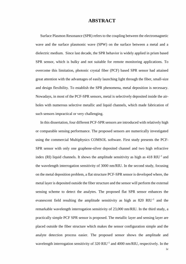
region and at the same time the positive ion will be moving as opposite to the electrons
as shown in Figure 2.1.
Figure 2.1: Plasmon oscillation in the metal (Jirí Homola, 2006).
Due to this moving mechanism a longitudinal oscillation will be introduced in the
conductor and this is known as the plasma oscillation which is known as surface plasmons
(Jiří Homola, 2003; Khan, 2012).
2.2.2 Surface Plasmon Resonance
To support the surface plasmons, a conductor and dielectric interface is required. In
general a metal and dielectric interface is used to support the surface plasmon oscillation.
Due to this oscillation and a certain resonance condition, surface plasmon wave is
generate which propagate along the surface (Figure 2.2). This surface plasmon is only
TM polarized electromagnetic field because for TE polarized case there is no solution of
the Maxwell’s equation. So for surface plasmon wave only the transverse magnetic (TM)
polarized electric field exists. This wave is decayed exponentially in the metal. This
Surface Plasmon Wave (SPW) is characterized by the propagation constant as (Jiří
Homola, 2003; Sharma et al., 2007);
DM
DM
c (2.1)
+ + + - - - + + +x
z
Dielectric
Metal
0
9
where ω is the angular frequency, c is the speed of light in vacuum and εM, and εD are the
dielectric permittivity’s of metal and dielectric medium, respectively.
According to the above equations, property of the SPW is dependent on the property of
two materials i.e. the metal and dielectric media.
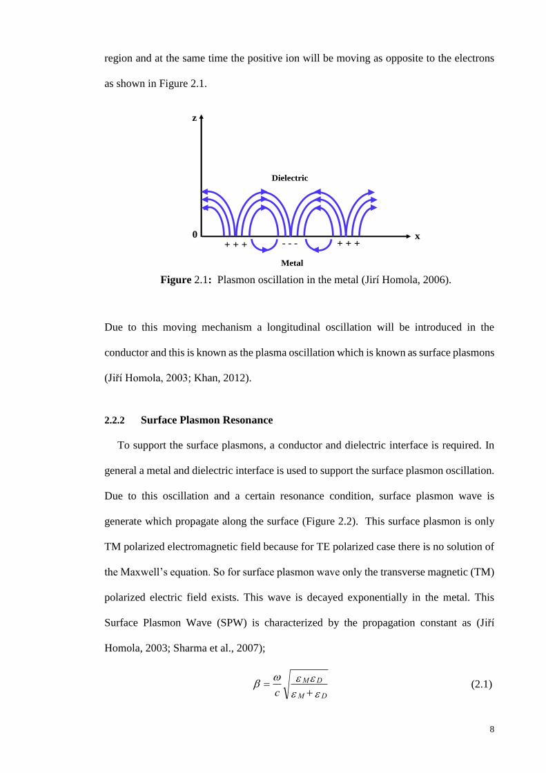
Figure 2.2: Localized SPR when field (light) interacts with the plasmons (Jirí
Homola, 2006).
Now to create the surface plasmon oscillation need to excite the electrons in the
conductor. So, impose the light (EM field) is necessary on the surface. We know that the
electrical permittivity for the conductor (metal) is negative and the electrical permittivity
for the dielectric is positive. In the dielectric medium the propagation constant
(maximum) can be written as (Emmerich; Sharma et al., 2007),
Sc
(2.2)
So it is stated that the propagation constant for surface plasmon wave is higher than
the propagation constant of light in the dielectric medium. As a result, surface plasmon
can’t be excited with the normal light; it requires the light with extra momentum or energy
with the same polarization state as the surface plasmon wave. Moreover, the propagation
constant should be matched with the surface plasmon wave.
- - -
- - -
+ + +
+ + +
Electric field
Electric cloud
Metal sphere
10
2.3 The Maxwell’s eigenvalue problem
Light can be observed as two aspects: it is an electromagnetic wave and it has particle
like property. Electromagnetic wave propagation in PCFs are based on the Maxwell’s
equations (D. K. Cheng, 1989). The analysis of the cylindrical coordinate system is given
below:
0. B (2.3)
D. (2.4)
0
t
BE (2.5)
jt
DH
(2.6)
Here, the electric and magnetic fields are represented by E and H, respectively. Electric and
magnetic flux densities are represented by D and B, respectively.
The flux densities can be expressed as,
rErrD 0 (2.7)
rHrrB 0 (2.8)
Here, ε(r) and μ(r) are known as the relative permittivity and permeability of the medium
and these properties are dimensionless. In contrast, ε0 and μ0 are the relative permittivity and
permeability in a free space where the values are ε0 = 8.854×10⁻¹² (F/m) and μ0 = 4π×10-7
(H/m).
Generally, permeability, μ(r) of the dielectric material is close to unity resulting the Eq. 2.8
can be written as B(r) = µ0H(r). The imaginary part of ε expresses the material related losses
but, for the low loss dielectric such as Silica, it is considered purely real. By assuming in a
medium there have no light source, free charges or current in the system, so ρ = 0 and J = 0.
By considering all assumptions, Eqs. 3.1-3.4 can be rewritten as:
0),(. trH (2.9)

11
0)],()(.[ trEr (2.10)
0),(
),(. 0
t
trHtrE (2.11)
0),(
)(),(. 0
t
trHrtrH (2.12)
The linearity of Eqs. 2.9-2.12 allow for the Fourier analysis. Any general solution can be
expressed as the combination of a set of harmonic modes at a different specific optical
frequencies. Temporal dependency can be removed from the original problem such as,
jwterHtrH )(Re),( (2.13)
jwterEtrE )(Re),( (2.14)
By the substitution of Eqs. 2.9-2.12 into Eqs. 2.13-2.14, following two divergence and
two curl equations are obtained:
0)(. rH (2.15)
0)]()(.[ rEr (2.16)
0)()( 0 rHjrE (2.17)
0)()()( 0 rHrjrH (2.18)
By combining two curl Eqs. 2.17 and 2.18, the master equation is obtain where the only
unknown parameter is H(r),
)()()(
12
rHc
rHr
(2.19)
In a system if the ε(r) is known then by following this master equation H(r) can be obtained.
Considering the z-invariant, system can be expressed as,
zjeyxHrH ),()( (2.20)
Here, along the z-direction propagation constant is β, Eigenvalue problem can be solved by
using the eigenvalue of β or ω. Considering the medium is homogenous such as ε(r, ω) =

12
ε(ω), the master equation Eq. 2.19 becomes a well-known scalar Helmholtz equation which
is able to analytically solve the single coordinate either cylindrical or cartesian coordinates.
Generally, the step index fiber, waveguide slab (Snyder & Love, 2012) and Bragg fiber (Yeh,
Yariv, & Hong, 1977) and structure could be analytically solved by the master equation Eq.
2.19 whereas PCFs analytical expression of boundary condition is quite complex due to the
spatial refractive index profile resulting the analytical solution is not possible to investigate
the optical properties of the PCFs. Finally, to investigate the optical properties of PCFs
structures, numerical methods need to be applied to solve the master Eq. 2.19.
2.4 Overview of Numerical Methods
A lot of numerical works already been carried out for the PCFs simulation. To
investigate the PCFs properties, several numerical methods are available. Accuracy of
these numerical methods are depends on some basic properties as describe below:
Full vector formulation: Full vector formulation allows the study of fibers with
arbitrary structural parameters as well as arbitrary refractive index contrast. Based
on the applications, structural parameters can be changed and controlled light
guiding.
Direct insertion: It facilitates for getting the results more accurate and
comparable with the experimental result. It permits the dependency on
wavelength with respect to refractive index. This property is important for
dispersion and confinement loss calculation.
Confinement loss (CL) measurement: Confinement loss measurement is one of
the most important property among all other PCFs properties. PCFs applications
are related to the light matters. If the loss is high then the launching light will
disappear immediately. It will not able to pass through the fiber as a result, it will
not be applicable for any of the applications.
13
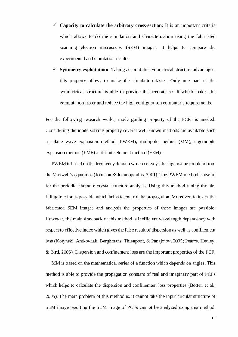
Capacity to calculate the arbitrary cross-section: It is an important criteria
which allows to do the simulation and characterization using the fabricated
scanning electron microscopy (SEM) images. It helps to compare the
experimental and simulation results.
Symmetry exploitation: Taking account the symmetrical structure advantages,
this property allows to make the simulation faster. Only one part of the
symmetrical structure is able to provide the accurate result which makes the
computation faster and reduce the high configuration computer’s requirements.
For the following research works, mode guiding property of the PCFs is needed.
Considering the mode solving property several well-known methods are available such
as plane wave expansion method (PWEM), multipole method (MM), eigenmode
expansion method (EME) and finite element method (FEM).
PWEM is based on the frequency domain which conveys the eigenvalue problem from
the Maxwell’s equations (Johnson & Joannopoulos, 2001). The PWEM method is useful
for the periodic photonic crystal structure analysis. Using this method tuning the air-
filling fraction is possible which helps to control the propagation. Moreover, to insert the
fabricated SEM images and analysis the properties of these images are possible.
However, the main drawback of this method is inefficient wavelength dependency with
respect to effective index which gives the false result of dispersion as well as confinement
loss (Kotynski, Antkowiak, Berghmans, Thienpont, & Panajotov, 2005; Pearce, Hedley,
& Bird, 2005). Dispersion and confinement loss are the important properties of the PCF.
MM is based on the mathematical series of a function which depends on angles. This
method is able to provide the propagation constant of real and imaginary part of PCFs
which helps to calculate the dispersion and confinement loss properties (Botten et al.,
2005). The main problem of this method is, it cannot take the input circular structure of
SEM image resulting the SEM image of PCFs cannot be analyzed using this method.

14
Moreover, this method cannot take the advantages of symmetrical structure. As a result,
partial part computational cannot give the accurate result (White et al., 2002).
EME is based on the frequency domain. It decomposes the electric field and make a
set of local eigenmodes which is exist in the cross-section of waveguide. EME algorithm
is bi-directional even it could be worked as omnidirectional if the adequate modes are
used. It is full-vectorial algorithm which facilitate the parameter variation as well the
effective index contrast variation. This method is useful to simulate the propagation of
twisted waveguide structure and it can simulate even 90 degree angle of propagation. This
method allows taking the advantages of symmetrical structure which reduces the
computational time. Using this EME method with interactive techniques nonlinear
problems can be modeled but this method is limited to the linear problems (Gallagher &
Felici, 2003).
FEM is a technique which is able to find the solution of partial differential equation
(PDE) to handle the boundary-value problem (Koshiba, 1992). The main advantage of
this method is that, it divides the computational area in a small finite region such as
triangles, rectangles etc., which allows to precisely analyze the structure. This method
allows to change the air-fill fraction and able to calculate the complex and real effective
index of the structure which gives the approximation of PCFs dispersion and propagation
behavior. Additionally, it is able to import and analyze the SEM image of fabricated PCFs
(Koshiba & Saitoh, 2001). In this research work, FEM based commercial COMSOL
software is used to develop the sensors as well as analyzing the sensor performance.
Table 2.1 shows a summary comparison between the PWEM, MM, EME and FEM
methods.

15
Table 2.1: Comparison among the numerical methods for the study of MOFs.
Properties PWEM MM EME FEM
Fully vectorial √ √ √ √
Material dispersion × √ √ √
CL calculation × √ × √
Arbitrary cross-section √ × √ √
Symmetry exploitation × × √ √
References (Johnson &
Joannopoulos,
2001; Pearce
et al., 2005)
(White et al.,
2002)
(Gallagher
& Felici,
2003)
(Koshiba,
1992;
Koshiba &
Saitoh, 2001)
2.5 Conventional Sensing Techniques of Surface Plasmon Resonance
Conventional SPR sensors are utilized using prism. Prism is used to concentrate the
incident light. When the p-polarized or TM light is incident on prism-metal dielectric
interface and the reflectance is measured as a function of angle of incidence, a sharp dip
is obtained at a particular angle called the resonance angle. The unknown analyte (analyte
is a substance or chemical component that is undergoing analysis) could be detected by
measuring the shift of resonance angle. This method is called the angular interrogation
method. Based on this sensing mechanism two sensing methods are developed, such as
(1) Otto-configuration, and (2) Kretschmann-configuration.
2.5.1 Otto-configuration for SPR sensing
In 1968, Otto introduced a prism coupling technique where the prism and metal were
placed in a gap and the gap was filled with the sample liquid (Figure 2.3) (Otto, 1968).
The sample liquid refractive index should be smaller than the prism. Otto configuration
is followed the attenuated total reflection (ATR) method. When the p-polarization light
is incident on the prism-dielectric interface it produces the evanescent wave (EW), at a

16
particular angle this evanescent wave excite the surface plasmon wave on the metal-
dielectric interface.
Figure 2.3: Otto-configuration for SPR sensor (Jirí Homola, 2006).
At a particular angle wave-vector of evanescent wave and surface plasmon waves are
matched together, at this angle a dip in reflected wave intensity can be observed. At this
condition, energy transfer from the EW to SPW. At the prism-dielectric interface wave
vector Kev of the evanescent field is given as,
singevc
k (2.21)
where ω is the frequency of incident light, c is the speed of light, εg is the dielectric
constant of the material of the prism and the incident angle is θ.
Otto-configuration has been found interesting for studying single crystal metal surfaces
and absorption on them. To utilize this prism-coupling, prism and metal layer should be
placed with a finite gap which is a drawback of Otto-configuration. By solving this
problem a modified configuration is introduced which is known as Kretschmann-
configuration.
Incident Light (p-polarized) Reflected Light
θ
EW
SPW
Prism
Metal Layer
εg
εs
εm
Sensing Medium

17
2.5.2 Kretschmann-configuration for SPR sensing
In 1968, Kretschmann-configuration had been introduced where the prism and metal
layer was attached together (KretschmannE, 1968), between the prism and metal layer
there was no gap; sample liquids were placed outside the metal layer (Figure 2.4).
Figure 2.4: Kretschmann-configuration for SPR sensor (Jirí Homola, 2006).
In this method, surface plasmons also excited by the evanescent wave like as Otto-
configuration. At a specific angle when the wave vector of evanescent wave and the
surface plasmon wave matched then the resonance was occurred, at this resonance
condition a dip reflected light intensity was also appeared. Incident light wave vector
which travelling along the prism surface is kg and the evanescent field wave vector, kev is
defined as;
sinsin ggevc
kk (2.22)
The main drawback of Kretschmann-configuration is metal layer should be parallel to
prism surface, thereby, this technique is not applicable for curved surfaces such as a metal
cylinder or metal sphere. This is one of the reasons why this configuration has not been
widely used (Knoll, 1998).
Incident Light (p-polarized) Reflected Light
θ
SPW
Prism
Sensing Medium
εg
εm
εs
Metal Layer

18
2.5.3 Problems Encountered
Otto and Kretschmann configurations are well developed for SPR sensor. Their
practical implementation are simple due to outer metal coating and also the plain surface
which is quite straight-forwat for metal deposition. However, prism based SPR sensor
has a lot of drawbacks such as it is bulky in size and it has a various optical and mechnical
moving parts which limits optimization and commercialization in a large scale (Dash &
Jha, 2014b). Due to its optical and mechanical moving parts, it is not suitable moving the
setup configuration outside the laboratory to detect the sample, which limits the
commercialization. Additionally, prism based SPR sensor couldn’t applicable for remote
sensing applications (Gupta & Verma, 2009).
2.6 Prism based SPR Sensing Mechanism
As described in previous section, prism based SPR sensor resonance is occurred when
the propagation constant of evanescent wave and the propagation constant of the surface
plasmon wave are the same. According to the Kretschmann-setup propagation constant
of evanescent wave is,
sinsin ggevc
kk (2.23)
Additionally, based on the Maxwell’s equation propagation constant, ksp of surface
plasmon waves which propagate along the metal-dielectric interface can be expressed as
(Jie, Dakai, & Zhenwu, 2007);
sm
smsp
ck
(2.24)
where εm is the dielectric constant of the dielectric medium or sensing medium and εs is
the dielectric constant of the metal.
At the resonance condition, equation (2.3) will be kev=kg. Based on the previous
discussion the resonance will occur at the following condition (Zhao, Deng, & Li, 2014),
19
sm
smresg
cc
sin (2.25)
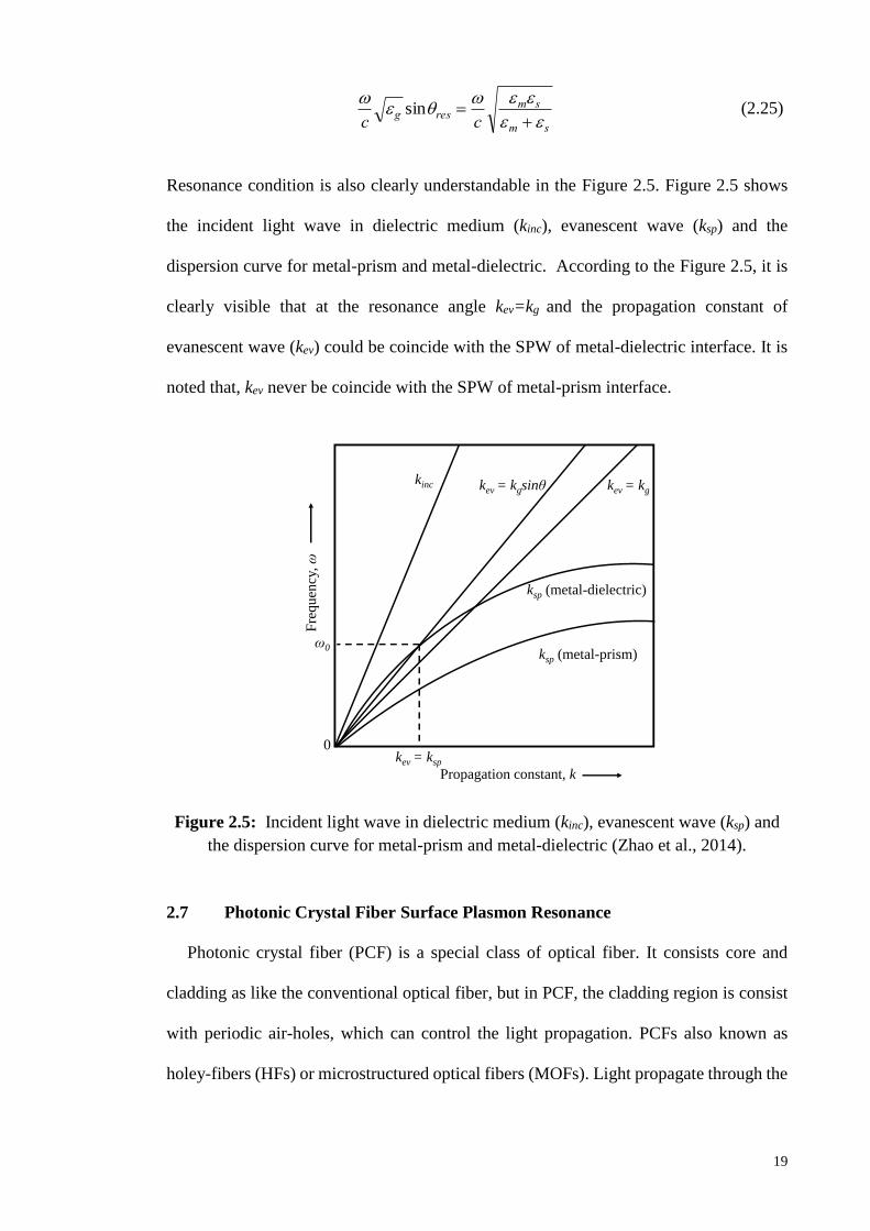
Resonance condition is also clearly understandable in the Figure 2.5. Figure 2.5 shows
the incident light wave in dielectric medium (kinc), evanescent wave (ksp) and the
dispersion curve for metal-prism and metal-dielectric. According to the Figure 2.5, it is
clearly visible that at the resonance angle kev=kg and the propagation constant of
evanescent wave (kev) could be coincide with the SPW of metal-dielectric interface. It is
noted that, kev never be coincide with the SPW of metal-prism interface.
Figure 2.5: Incident light wave in dielectric medium (kinc), evanescent wave (ksp) and
the dispersion curve for metal-prism and metal-dielectric (Zhao et al., 2014).
2.7 Photonic Crystal Fiber Surface Plasmon Resonance
Photonic crystal fiber (PCF) is a special class of optical fiber. It consists core and
cladding as like the conventional optical fiber, but in PCF, the cladding region is consist
with periodic air-holes, which can control the light propagation. PCFs also known as
holey-fibers (HFs) or microstructured optical fibers (MOFs). Light propagate through the
0kev = ksp
Propagation constant, k
ksp (metal-prism)
Fre
qu
ency
, ω
ω0
ksp (metal-dielectric)
kev = kgkev = kgsinθkinc
20
PCFs follow the modified total internal reflection (M-TIR) or photonic band gap (PBG)
effects.
Since last decade, PCF SPR sensor has been shown great attention. PCF SPR sensor
is the combination of PCF technology and the plasmonic science. SPR sensors require a
metallic component carrying large amounts of free electrons. These free electrons provide
the real part of a negative permittivity which is essential for plasmonic materials. By
introducing the plasmonic metal layer coating inside the air-holes surface or the outer
surface of the PCFs structure SPR effects could be realized.
2.7.1 Advantages of Photonic Crystal Fiber Over Prism
Prism based SPR sensors are worked based on angle interrogation method. At a
specific angle when the wave vector of EW and SPW are matched then the resonance is
occurred and a reflected wave is generated. In practice, light lunching in a specific angle
is difficult. Moreover, its structure also bulky. To solve those problems PCFs have shown
great attention since last few decades. By harnessing the advantages of PCFs such as small-
size and design flexibility, it is possible to control the evanescent field. Based on the
applications, core-guided leaky-mode propagation can be controlled by using different
types of PCF’s structures such as hexagonal, square, octagonal, decagonal, hybrid, etc.;
and also their guiding properties can be controlled by optimizing the structural parameters
(Ahmmed, Ahmed, & Razzak, 2013; Aoni, Ahmed, & Razzak, 2013). Optimizing core-
clad diameter or position, light propagation in single mode as well as launching light at
zero incidence angle into the core to excite SPs are possible. Single mode PCFs show
very sharp resonance peak, which enhance the detection accuracy (Slavık, Homola, &
Čtyroký, 1999). Besides, sensitivity and sensing range could be increased by optimizing
the structural parameters.

21
2.7.2 Sensing Mechanism of PCF SPR Sensor
PCF based SPR sensors are working based on evanescent field. When the light
propagates through the core by following the total internal reflection then a part of the
electromagnetic filed that propagates from the cladding is called the evanescent field. In
PCF SPR sensor structure, evanescent field penetrate through the cladding region and hit
on the plasmonic metal surface which excite the free electrons of the metal surface. When
the frequency of the incident photon and the frequency of the free electrons are matched,
the electrons start to resonate and at this condition surface plasmon wave is generated on
the metal-dielectric interface, this is called the resonance condition. At this resonance
condition, a sharp loss peak is appear which is very sensitive with the adjacent dielectric
layer of metal layer. Mathematically, resonance will occur when the real effective
refractive index (neff) of core-guided mode and surface plasmon polaritons (SPP) mode
value are exactly the same. At the resonance condition, maximum energy transfer from
the core-guided mode to the SPP mode. Due to the change of refractive index of dielectric
media (sample media), neff of SPP will change resulting the loss peak and the resonant
wavelength shift. This indicates the phase matching wavelength changes with the change
of sample/analyte refractive index. Unknown sample could be detected by observing the
variation of loss peak due to change of analyte RI.
2.8 Implementation of PCF SPR Sensor
PCF SPR sensor is the combination of PCF technology and the plasmonic science. In
practice, PCF can be fabricated by following the standard Stack-and-Draw fiber drawing
method (G Amouzad Mahdiraji et al., 2014) and plasmonic metal layer coating can be
carried out by following the high pressure chemical vapor deposition (CVD) method
(Sazio et al., 2006) or sputtering method (Malinský, Slepička, Hnatowicz, & Švorčík,
2012). Numerical implementation of PCF SPR sensor structure is described below.

22
2.8.1 PCF Structure Implementation
2.8.1.1 Geometrical Definition
First step is to design the PCFs according to the design rules such as for the hexagonal
PCFs structure, the vertex angle of triangle (triangle has two legs in equal distance) would
be 600 while for the octagonal and decagonal PCFs this angles would be 450 and 300
shown in Figure 2.6. In the PCFs, air-holes are arranged in a periodic form with the
diameter of d. Two adjacent air-holes distance is known as pitch and defined as Λ.
Figure 2.6: (a) and (b) Cross-section view and unit triangle of hexagonal PCF
respectively; (c) and (d) cross-section view and unit triangle of octagonal PCF
respectively; (e) and (f) cross-section view and unit triangle of decagonal PCF,
respectively.
For the realization of PCF SPR sensor phenomenon, plasmonic metal layer and a sensing
layer have to be considered. Metal layer thickness can be defined by t and the sensing
(a) (b)
(c) (d)
(e) (f)
23
layer thickness tna. In this stage, a Perfectly Matched Layer (PML) boundary region need
to be considered.
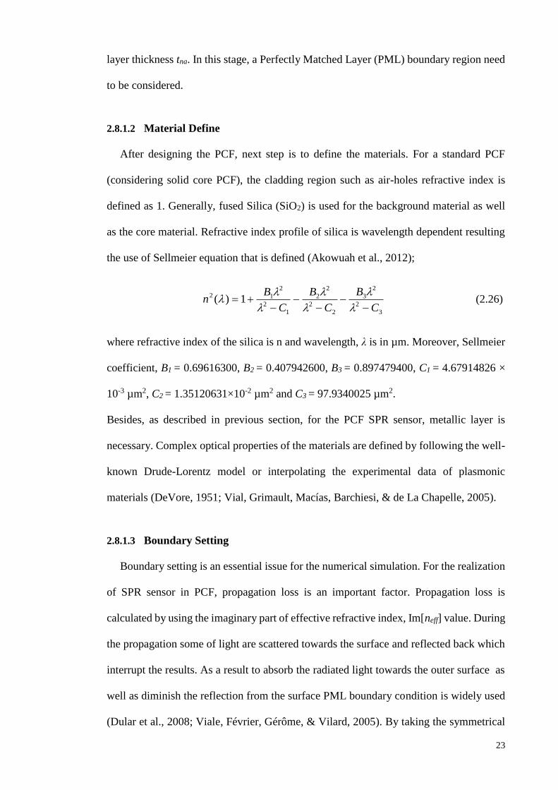
2.8.1.2 Material Define
After designing the PCF, next step is to define the materials. For a standard PCF
(considering solid core PCF), the cladding region such as air-holes refractive index is
defined as 1. Generally, fused Silica (SiO2) is used for the background material as well
as the core material. Refractive index profile of silica is wavelength dependent resulting
the use of Sellmeier equation that is defined (Akowuah et al., 2012);
3
2
2
3
2
2
2
2
1
2
2
12 1)(C
B
C
B
C
Bn
(2.26)
where refractive index of the silica is n and wavelength, λ is in µm. Moreover, Sellmeier
coefficient, B1 = 0.69616300, B2 = 0.407942600, B3 = 0.897479400, C1 = 4.67914826 ×
10-3 µm2, C2 = 1.35120631×10⁻² µm2 and C3 = 97.9340025 µm2.
Besides, as described in previous section, for the PCF SPR sensor, metallic layer is
necessary. Complex optical properties of the materials are defined by following the well-
known Drude-Lorentz model or interpolating the experimental data of plasmonic
materials (DeVore, 1951; Vial, Grimault, Macías, Barchiesi, & de La Chapelle, 2005).
2.8.1.3 Boundary Setting
Boundary setting is an essential issue for the numerical simulation. For the realization
of SPR sensor in PCF, propagation loss is an important factor. Propagation loss is
calculated by using the imaginary part of effective refractive index, Im[neff] value. During
the propagation some of light are scattered towards the surface and reflected back which
interrupt the results. As a result to absorb the radiated light towards the outer surface as
well as diminish the reflection from the surface PML boundary condition is widely used
(Dular et al., 2008; Viale, Février, Gérôme, & Vilard, 2005). By taking the symmetrical

24
structural benefits full structure can be divided by quarterly, and only one quarter able to
provide the accurate result which reduce the computational time. In such partial structure
artificial boundary condition such as electric field along the x-axis and magnetic field
along the y-axis can be used to determine the fundamental mode.
2.8.1.4 Meshing
Computational area can be divided into finite number of small triangular or rectangular
region which is known as mesh. Meshing is an important parameter to precisely
investigate the mode profile. In computational region where the light propagates,
precisely analyzing the propagation can be performed by increasing the mesh density of
the area. Number of mesh size indicates, how many mesh elements are used. Higher
number of mesh elements are better for the numerical simulation which indicates the
computational region is divided into the small region which increases the probability of
result accuracy.
2.8.1.5 Solving
As mentioned in previous section, commercial COMSOL multiphysics software is
used in this study. After going through all described process the final stage is to compute
the simulation. For the PCF SPR sensor need to find the core-guided mode and SPP mode.
Before the computation take place, the operational wavelength and the number of
searching modes need to be specified. Number of searching mode allow to show the core-
guided fundamental mode and all the possible higher order modes. The modes over the
operational wavelength range of interest can also be calculated from the latest version of
COMSOL software. For calculating the confinement loss, the required data, i.e.,
imaginary effective index value can be extracted from COMSOL.

25
2.8.2 Combination of PCF with Plasmonic Science
By incorporating the thin metallic layer with the PCF structure, surface plasmon can
be established. Thin plasmonic metal layer is used inside the air-holes surface or the outer
surface of the fiber structure. Evanescent field of the core-guided mode excite the free
electrons of metal layer; while the frequency of the incident photon and the free electrons
frequency will matched then the surface plasmon resonance will occur. For the PCF SPR
sensor, to apply this resonance mechanism in sensing, a dielectric layer (sensing medium)
is considered sequentially top of the metal layer. Optical property of dielectric layer such
as refractive index (RI) is used. RI value of dielectric medium is sensitive to the neff of
SPP mode. Due to change of dielectric RI value, neff of SPP mode is change resulting the
resonance wavelength shift occurs. By observing this resonance shift unknown analyte
will be detected. This is the basic working principle of PCF SPR sensor.
2.8.3 Accuracy
To get the accurate result mesh size and PML convergence test have to be considered
(Poletti, 2007). For a simple PCFs structure by considering the default extremely fine
meshing elements are adequate to precisely investigate the mode profile. Nonetheless, for
the complex structure mesh convergence is necessary. Besides, PML convergence is an
important issue as it is use to absorb the radiation. For the PCF SPR sensors confinement
loss is the main factor to be determined. To measure the confinement loss, imaginary part
of the effective index (Im(neff)) value is necessary. Initially, due to increase of PML
thickness, Im(neff) value is change which may give the false result of confinement loss;
but, after a certain PML thickness with the increase of PML thickness. It gives the
constant Im(neff) value. As a result to calculate the accurate confinement loss of a
structure, PML thickness verification is necessary. Here, a proposed sensor is considered
which is described in details in Chapter 3. Cross-section of the proposed sensor is shown
in Figure 2.7(a) and the meshed structure is shown in Figure 2.7(b). For the verification

26
of PML thickness, the optimum thickness is determined by varying the PML thickness
from 0 - 20 μm. According to the Figure 2.7(c), initially with the increase of PML
thickness, imaginary neff values are rapidly changed, however a small variation in neff
value is observed by changing the PML thickness from 4 μm to 20 μm. As we know to
measure the loss of a PCF, Im(neff) value is the main parameter. In this range of PML
thickness (i.e., 4-20 μm), a very small Im(neff) variation of about 2 dB/cm is observed.
Thus, a PML thickness of 5 μm seems to be optimized for this structure for the better
radiation absorption. However, if a thicker PML region is considered compare to the
structure size then the core-guided light propagation is reduced. So, considering all the
issues PML convergence is needed for the accurate confinement loss measurement.
It should be noted that since the optimum PML layer thickness might be different in
different structures, a pre-optimization is performed per proposed designed in this study.
Figure 2.7: (a) Cross-section of the proposed PCF SPR sensor structure, (b) Meshing,
& (c) Imaginary effective index versus PML thickness for the core-guided fundamental
mode of the proposed PCF SPR sensor.
1.19E-04
1.19E-04
1.20E-04
1.20E-04
1.21E-04
1.21E-04
1.22E-04
1.22E-04
1.23E-04
0 4 8 12 16 20
Im(n
eff)
PML Thickness (μm)
PML layer
(a) (b)
(c)

27
2.9 Overview of PCF SPR Sensors
In the last few decades, SPR phenomenon attracted much attention due to its broad
range of sensing applications and high sensitivity. SPR sensor has shown remarkable
development in biosensing applications such as biomolecular analytes detection, medical
diagnostics, antibody-antigen interaction, etc. (Gupta & Verma, 2009; Jiří Homola, 2003;
Jiřı Homola, Yee, & Gauglitz, 1999; Wong, Krupin, Sekaran, Mahamd Adikan, & Berini,
2014). Generally, a prism coupling configuration with a thin layer of metal coating is
used as SPR sensor. Transverse magnetic or p-polarized light that is launched into the
prism will be coupled to the metal-dielectric interface when the phase matching condition
is met (Zhao et al., 2014). SPR technique for bio-sensing and gas detection was first
reported by Liedberg et al. (1983). However, prism based SPR sensor in the well-known
Kretschmann set-up is bulky and not suitable for remote sensing (Dash & Jha, 2014b).
PCF based SPR sensing technique is considered a possible route to miniaturization.
PCF has been proven as a good replacement of prism, having smaller footprint, easier
system integration and cost effective. In 2006, MOF based SPR sensor was introduced
for the first time (A Hassani & Skorobogatiy, 2006). Two ring, hexagonal PCF structure
was proposed where gold layers and liquid were infiltrated selectively in the 2nd ring,
shown in Figure 2.8(a). A small central air-hole was used to establish the phase matching
phenomena. Due to different guided modes three resonance peaks were appeared and the
1st resonance peak shown the highest resonance depth with the sensor resolution of 3×10-
5 RIU. To prevent the selective gold coating and liquid infiltration, honeycomb MOF had
been reported with the external sensing scheme, shown in Figure 2.8(b) (Gauvreau,
Hassani, Fassi Fehri, Kabashin, & Skorobogatiy, 2007). In this work, gold and sensing
layer has been placed outside the fiber structure to make the sensing process simple and
straight forward in practice. Using the PCF SPR phenomena detection of biolayer
thickness has been reported (Figure 2.8(c)) which is applicable for monitoring the

28
concentration of nanoparticles for the study of photodynamic cancer therapy (Alireza
Hassani & Skorobogatiy, 2009).
Figure 2.8: (a) & (d) Selectively gold coated and liquid-analyte filled PCF SPR
sensors (A Hassani & Skorobogatiy, 2006; Yu et al., 2010); (b) & (c) PCF SPR sensor
with external sensing approach (Gauvreau et al., 2007; Alireza Hassani & Skorobogatiy,
2009).
To enhance the phase matching between the core-mode and plasmonic mode and also to
enhance the detection accuracy selectively gold coated and liquid-analyte filled PCF SPR
sensor has been reported (Figure 2.8(d)) (Yu et al., 2010).
In 2011, silver nanowire based PCF SPR has been reported which overcome the metal
coating problem (Figure 2.9(a)) (Fu, Lu, Huang, & Yao, 2011). To show the positive and
negative refractive index sensor, liquid-core PCF has been reported (Shuai, Xia, & Liu,
2012). Six selective liquid-analyte filled core has been considered with one metallic
channel to exhibit the positive and negative RI sensitivity simultaneously (Figure 2.9(b)).
The maximum positive RI sensitivity of 3,600 nm/RIU in the sensing range of 1.45-1.46
(a) (b)
(c) (d)
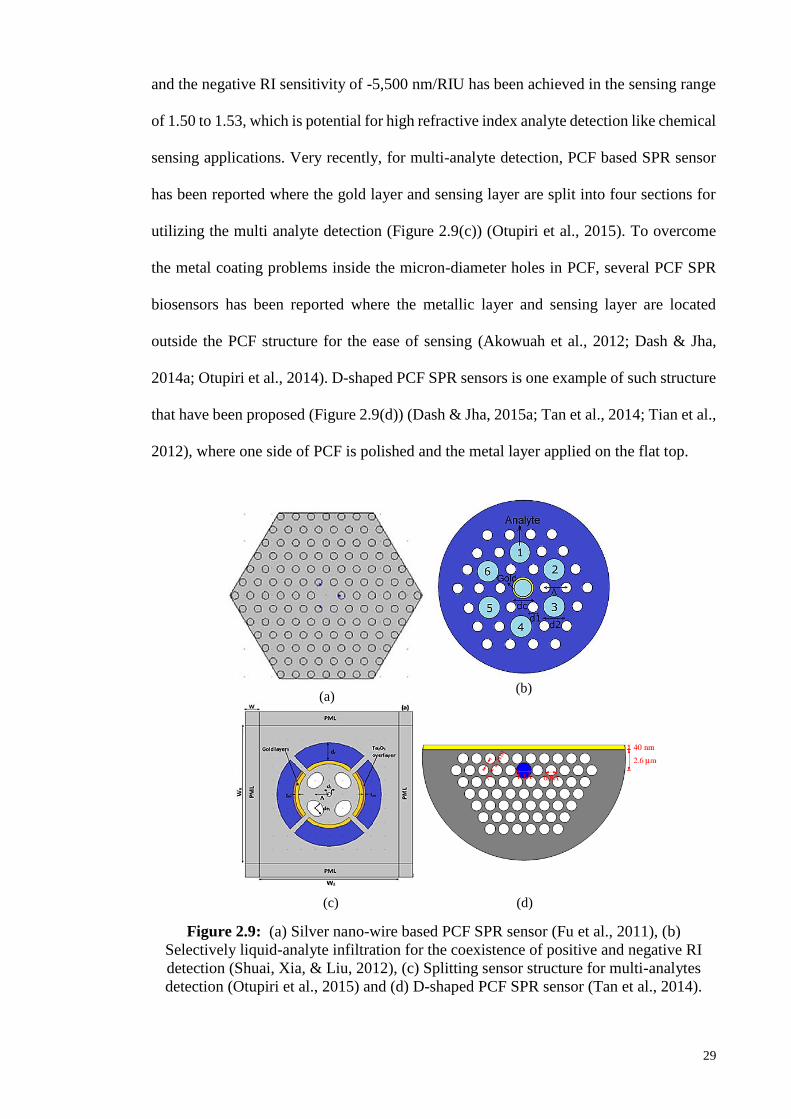
29
and the negative RI sensitivity of -5,500 nm/RIU has been achieved in the sensing range
of 1.50 to 1.53, which is potential for high refractive index analyte detection like chemical
sensing applications. Very recently, for multi-analyte detection, PCF based SPR sensor
has been reported where the gold layer and sensing layer are split into four sections for
utilizing the multi analyte detection (Figure 2.9(c)) (Otupiri et al., 2015). To overcome
the metal coating problems inside the micron-diameter holes in PCF, several PCF SPR
biosensors has been reported where the metallic layer and sensing layer are located
outside the PCF structure for the ease of sensing (Akowuah et al., 2012; Dash & Jha,
2014a; Otupiri et al., 2014). D-shaped PCF SPR sensors is one example of such structure
that have been proposed (Figure 2.9(d)) (Dash & Jha, 2015a; Tan et al., 2014; Tian et al.,
2012), where one side of PCF is polished and the metal layer applied on the flat top.
Figure 2.9: (a) Silver nano-wire based PCF SPR sensor (Fu et al., 2011), (b)
Selectively liquid-analyte infiltration for the coexistence of positive and negative RI
detection (Shuai, Xia, & Liu, 2012), (c) Splitting sensor structure for multi-analytes
detection (Otupiri et al., 2015) and (d) D-shaped PCF SPR sensor (Tan et al., 2014).
(a)(b)
(c) (d)
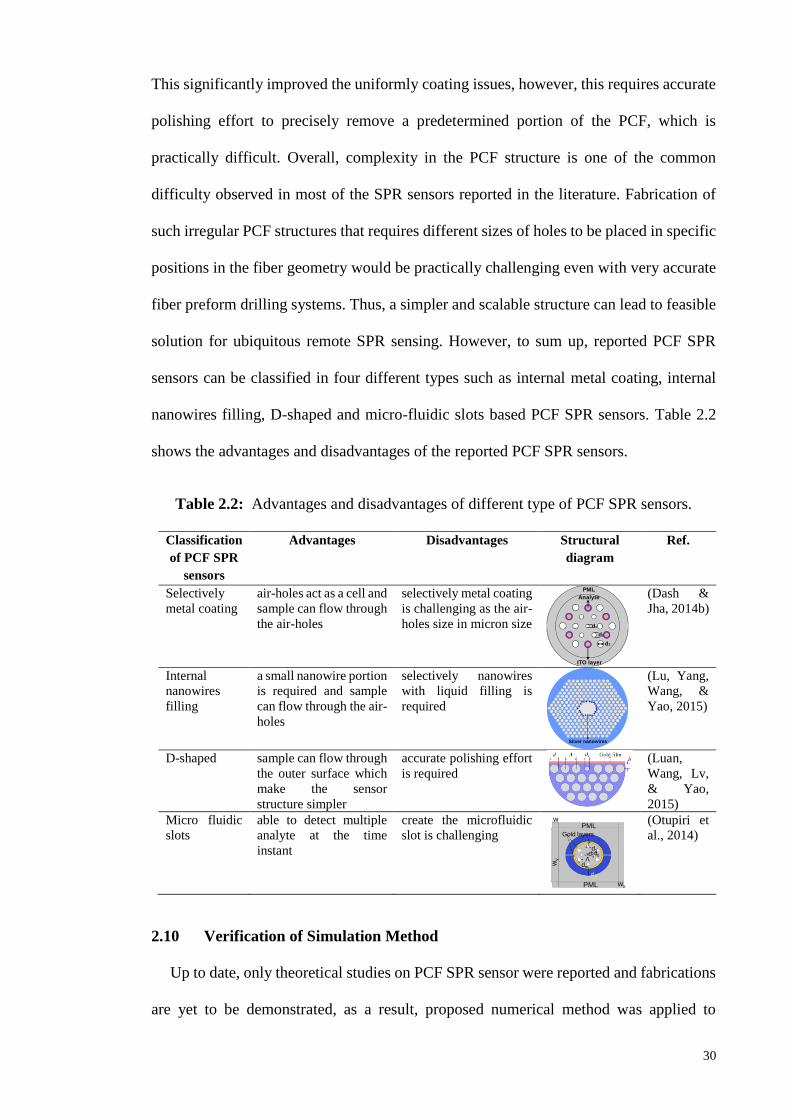
30
This significantly improved the uniformly coating issues, however, this requires accurate
polishing effort to precisely remove a predetermined portion of the PCF, which is
practically difficult. Overall, complexity in the PCF structure is one of the common
difficulty observed in most of the SPR sensors reported in the literature. Fabrication of
such irregular PCF structures that requires different sizes of holes to be placed in specific
positions in the fiber geometry would be practically challenging even with very accurate
fiber preform drilling systems. Thus, a simpler and scalable structure can lead to feasible
solution for ubiquitous remote SPR sensing. However, to sum up, reported PCF SPR
sensors can be classified in four different types such as internal metal coating, internal
nanowires filling, D-shaped and micro-fluidic slots based PCF SPR sensors. Table 2.2
shows the advantages and disadvantages of the reported PCF SPR sensors.
Table 2.2: Advantages and disadvantages of different type of PCF SPR sensors.
Classification
of PCF SPR
sensors
Advantages Disadvantages Structural
diagram
Ref.
Selectively
metal coating air-holes act as a cell and
sample can flow through
the air-holes
selectively metal coating
is challenging as the air-
holes size in micron size
(Dash &
Jha, 2014b)
Internal
nanowires
filling
a small nanowire portion
is required and sample
can flow through the air-
holes
selectively nanowires
with liquid filling is
required
(Lu, Yang,
Wang, &
Yao, 2015)
D-shaped sample can flow through
the outer surface which
make the sensor
structure simpler
accurate polishing effort
is required
(Luan,
Wang, Lv,
& Yao,
2015)
Micro fluidic
slots able to detect multiple
analyte at the time
instant
create the microfluidic
slot is challenging
(Otupiri et
al., 2014)
2.10 Verification of Simulation Method
Up to date, only theoretical studies on PCF SPR sensor were reported and fabrications
are yet to be demonstrated, as a result, proposed numerical method was applied to
PML
ITO layer
dc
d2
d1
Analyte
Silver nanowires
PML
PML
Gold layers
d3
dm
d1
d2
Λd0
wx
wy
w

31
reproduce the results reported in (Shuai, Xia, & Liu, 2012), which has been published in
well-known top ranked journal. Figure 2.10(a) shows the cross-section of reported PCF
SPR sensor where multi liquid-analyte channels have been used with the single gold
metallic channel.
Figure 2.10: (a) & (b) Cross-section of the published PCF SPR sensor and the phase
matching phenomena, respectively (Shuai, Xia, & Liu, 2012); (c) & (d) reproduced
cross-section view and phase matching phenomena, respectively.
Figure 2.10(b) shows the phase matching phenomena between the neff of core-guided
mode, SPP mode and loss peak which are the main criteria of PCF SPR sensor. As
shown in Figure 2.10(b), neff of core-guided mode, SPP mode and loss peak are matched
at the wavelength of 1040 nm while analyte na is 1.46. As described before, unknown
analyte will be detected by measuring the resonance wavelength shift due to analyte RI
changes. At the resonance wavelength loss value is achieved 68 dB/cm.
1.43
1.432
1.434
1.436
1.438
1.44
1.442
1.444
1.446
0
20
40
60
80
100
0.97 0.99 1.01 1.03 1.05 1.07 1.09
Re(
nef
f)(R
IU)
Loss
(dB
/cm
)
Wavelength (μm)
na=1.46, core mode
na=1.46, core mode
na=1.46, spp mode
(c)
(c)
(b)
(a)
(b)
(a)
(c) (d)

32
Figure 2.10(c) & (d) shows the reproduced cross-section outlook of PCF SPR sensor
and the phase matching phenomena respectively. According to Figure 2.10(d), phase
matching wavelength is appear at 1.04 μm while the analyte na is 1.46; this is exactly
same as the reported result. According to the reproduced structure, peak loss value
shows 88 dB/cm which is a little bit larger than the reported works. The peak loss value
difference is occurred due to the fiber diameter and PML thickness are unknown and
here convergence test has been used to reproduce the result. In Figure 2.10 (b) & (d),
inset(c) shows the energy transfer from the core-guided mode to the SPP mode which
is almost same, furthermore, core-guided mode and SPP mode propagation also alike
both of the works. Based on the discussion and the reproduced results, the
computational method which is following for this research work is correct.
2.11 Optical Properties and Metallic Films
As described in previous sections, metal is the important element for the plasmonic
behavior. SPR sensors require a metallic component carrying large amounts of free
electrons, these free electrons provide the real part of a negative permittivity which is
essential for plasmonic materials. Generally, novel material gold (Au), silver (Ag), copper
(Cu) and aluminum (Al) are widely used as the plasmonic material. Generally metals are
prone to oxidize due to presence of aqueous environment, water, humidity, and etc. For
the SPR sensing applications Au and Ag are comprehensively used. Gold is chemically
stable in aqueous environment. Also, it shows a larger resonance peak. However, it shows
the broaden resonance peak which may give the false positive analyte detection result as
a result detection accuracy is diminish (Dash & Jha, 2014a). Besides, Ag shows a sharper
resonance peak. It is utmost conductive and its material losses are less among the
available materials. However, it has oxidation problem, owing presence of aqueous
environment it oxidizes easily which reduces the sensing performance (Naik, Shalaev, &
Boltasseva, 2013). Copper is the 2nd most conductive material after the silver. It is much

33
cheaper compared to both gold and silver. Cu material damping rate is the same as Au,
and its interband transition is also close to Au (West et al., 2010). Cu also has oxidation
problem which is the main reason hence it is not received great attention compared to Au
and Ag. The oxidation problem can be solved by using a thin bimetallic layer coating top
of the Ag or Cu surface (Zynio, Samoylov, Surovtseva, Mirsky, & Shirshov, 2002). In
contrary, as the plasmonic material Al didn’t receive that much of attention as its damping
rate is very high as well as its material losses also high. As a result, it did not attain
attention for the sensing applications (West et al., 2010).
2.12 Summary
In this chapter, basic properties of surface plasmon and Maxwell’s master equation is
derived to investigate the light traveling properties. Conventional SPR sensors working
mechanism and problems are discussed. In addition, advantages of PCF over prism in
SPR sensing are labelled. A brief literature review on PCF based SPR sensors are given
in this chapter. Importance and the status of the plasmonic materials are outlined.
Numerical methods are described and compared based on the mode propagation property
of PCFs. PCF SPR sensor implementation is carried out in details to understand the
design procedure. Furthermore, design convergence is described which helps to get the
accurate results and validate the proposed method by reproducing the reported literature
results. To sum up, conventional prism based SPR sensor problems can be solved by
using PCF. However, yet, reported PCF based SPR sensors structure are challenging in
terms of fabrication point of view which limits the practical implementation.

34
CHAPTER 3: GRAPHENE-SILVER DEPOSITED
PLASMONIC SENSOR
3.1 Introduction
In this chapter a fiber Surface Plasmon Resonance sensor based on PCF with
selectively filled analyte channels is proposed. Silver is used as the plasmonic material to
accurately detect the analytes and is coated with a thin graphene layer to prevent
oxidation. The liquid-filled cores are placed near to the metallic channel for easy
excitation of free electrons to produce SPWs. Surface plasmons along the metal surface are
excited with a leaky Gaussian-like core guided mode. Numerical investigation of the
fiber’s properties and the sensing performance is performed with FEM. The effects of
fiber structural parameters on the properties of plasmonic excitation are investigated and
optimized for the sensing performance as well as reducing the sensor’s footprint.
3.2 Literature Review
In the last few decades, photonic biosensors had shown remarkable developments in
various applications such as medical diagnostics, bio-chemical detection and organic
chemical detection (Akowuah et al., 2012; Jiří Homola, 2003; Kim et al., 2013; Ortega-
Mendoza et al., 2014). To date, several sensing techniques are available such as micro-
ring resonator sensor (Yuan et al., 2014), surface plasmon resonance (SPR) sensor
(Akowuah et al., 2012; Jiří Homola, 2003), evanescent wave absorption spectroscopy,
etc. Surface plasmons (SPs) are the collective oscillations of free electrons that propagate
along a metal-dielectric interface by satisfying certain resonance conditions (Daghestani
& Day, 2010; Jiří Homola, 2003). The first SPR experiment for bio-sensing and gas
detection was reported by Jorgenson and Yee (1993), since then, SPR has been given
much attention due to its extremely sensitive performance. In the conventional
35
Kretschmann SPR configuration, a coupling prism with a thin metal-deposited base is
used, in the presence of incident light at a specific angle; SPs will be excited on the metal-
dielectric interface. However, the conventional SPR configuration is bulky and not
suitable for remote sensing, which limits its large scale fabrication for real time
application (Dash & Jha, 2014b).
To overcome these limitations, the feasibility of fiber-based SPR sensor in sensing
application is explored. Besides, increasing the sensitivity and enhancing the sensing
range are possible by optimizing the PCF structural parameters. Phase matching between
the core-guided mode and the surface plasmon polaritons (SPPs) mode could be achieved
by carefully designing the fiber structure. In general, a sharp loss peak appears at phase
matching wavelength enables the sample analyte to be detected (Gupta & Verma, 2009).
The sensing performance depends highly on the choice of plasmonic materials, in most
cases, gold and silver are used. Gold is chemically stable and shows larger resonance
peak shift as compared with the other active plasmonic materials. However, due to the
large absorption coefficient, resonance band of gold is broader, which reduces the sensing
accuracy. The other problems associated with gold including the formation of island in
thin gold layer, band to band transition and surface roughness due to thermal evaporation
(Dash & Jha, 2014b; Kanso, Cuenot, & Louarn, 2007). On the contrary, silver shows
sharper resonance peak as compared with the other plasmonic materials. Nonetheless,
silver is not chemically stable and could be oxidized easily (Lu et al., 2013). Silver film
with graphene coating has shown to solve the problem of oxidation since graphene is
impermeable to gas molecules as small as Helium and therefore inhibits the passing of
oxygen (Choi, Kim, & Byun, 2011). Furthermore, graphene coating applied on the metal
surface can improve the sensing performance due to its high surface to volume ratio.
Besides, it increases the absorption of analyte molecules owing to the π-π stacking and
possesses superior plasmonic properties that are suitable for sensing (Dash & Jha, 2014a;

36
Maharana & Jha, 2012; Salihoglu, Balci, & Kocabas, 2012). Fiber-based plasmonic
phenomenon realized by replacing the metal film with graphene was first reported by
Kim et al. (2013), where a thin graphene layer was created by using thermal chemical
vapor deposition (TCVD) technique. Sensing performance improvement of SPR sensors
with graphene coating on top of Au/Ag compared with the SPR sensors without graphene
coating are also reported (Dash & Jha, 2014a; L. Wu, Chu, Koh, & Li, 2010). Recently,
gold is used as an active plasmonic material and selectively infiltrating the core of PCF
with high refractive index (RI) analyte to introduce the coexistence of positive and
negative RI (Shuai, Xia, & Liu, 2012). On the other hand, different fiber structures with
enhanced evanescent field in the fiber based SPR sensor were reported. They are elliptical
air-hole PCF sensor with four separated microfluidic slots (Akowuah et al., 2012); multi-
hole fiber SPR sensor where all the holes are coated with gold and titanium dioxide (Gao
et al., 2014); selectively six metal oxide coating and liquid infiltration inside the six-air-
hole with four different sizes of capillary holes in a polymer PCF (Dash & Jha, 2014b);
and a seven-air-hole liquid infiltration with six metal oxide coating (Qin et al., 2014).
However, the abovementioned fiber-based SPR sensors are difficult to be fabricated due
to both complex fiber structure and the existence of several metallic channels.
In this chapter, a simple liquid core PCF plasmonic sensor with selectively filled
analyte channels is proposed. Silver layer with graphene coating is used to improve the
sensing performance. Proposed sensor shows higher amplitude sensitivity as compared
with reported works in (Gao et al., 2014; Alireza Hassani, Gauvreau, Fehri, Kabashin, &
Skorobogatiy, 2008) and higher wavelength interrogation sensitivity than sensors
reported in (Biswas, Chattopadhyay, & Bhadra, 2014; Dash & Jha, 2014b; Lu et al.,
2012). The metallic channel, liquid cores, and unique air holes arrangement of the
proposed sensor introduce larger evanescent field that results in stronger coupling
between the core-guided mode and the SPP mode.

37
3.3 Methodology
3.3.1 Structural Design and Numerical Analysis
Figure 3.1: Cross-section of the proposed (a) sensor, (b) stacked preform.
Figure 3.1(a) shows the cross-section of the proposed fiber sensor. Two identical cores
are filled with high RI liquid (analyte) and form a straight line with the center metallic
channel. The proposed structure couples core-guided mode and plasmonic mode at the
interface of silver-graphene layer and the analyte. The air-holes are distributed in
triangular lattice where the distance between adjacent air-holes (lattice constant, pitch) is
Λ=1.90 μm and the air-hole diameter is d=0.5Λ. The analyte core diameter and the
metallic channel diameter are similar, d1=dc=0.8Λ. Liquid-filled hole diameter is larger
than the other air-holes to simplify the flow of the analyte through them. Silica (SiO2) RI
profile is approximated by the Sellmeier equation (Otupiri et al., 2014). A graphene layer
on top of a thin silver layer is used at the inner wall of the fiber central core. The silver
and graphene thicknesses are set as tag=35 nm and tg=3 nm, respectively. The RI of silver
is adopted from (Palik, 1998) and the complex RI of the graphene is determined from the
equation: ng=3+iC1λ/3, where λ is the vacuum wavelength in µm and constant C1≈5.446
μm-1. To analyze the guiding properties of the proposed sensor, FEM is used by
considering PML boundary condition as a radiation absorber. By taking the advantage of
the symmetrical structure, we compute only a quarter of the proposed structure to reduce
the computation time. Perfect electric conductor (PEC) and perfect magnetic conductor
(a) (b)
38
(PMC) boundary conditions are used at the horizontal and vertical outer boundaries
respectively.
3.3.2 Realization of the Proposed Sensor
Fabrication of the proposed fiber structure is possible using the standard stack-and-
draw method (G Amouzad Mahdiraji et al., 2014). The two larger cores and the central
metallic channel can be realized by introducing thinner wall capillaries compared to the
other capillaries during the stacking process, as illustrated in Figure 3.1(b). The
deposition of metal layers on the inner surface of the air-holes in the proposed structure
is possible by applying the high pressure CVD technique, thermal evaporation, sputtering
technique, electroless plating technique or wet-chemistry technique (Sazio et al., 2006;
Takeyasu, Tanaka, & Kawata, 2005). Deposition of graphene layer in the capillary would
also be possible by using the CVD method. Ismach et al. had realized graphene layer on
dielectric surface using CVD method (2010). Deposition of graphene on microfiber had
also been reported by Y. Wu et al. (2014). Besides, growing graphene on silver had been
demonstrated by Kiraly et al. (2013). The liquid selective infiltration of single-hole (Guo
et al., 2014) and multi-holes (Vieweg et al., 2010) in PCF are also reported by using two-
photon direct laser writing and direct manual gluing method. The proposed sensor can
be calibrated with a liquid with known RI and using the flow cell analyte containing
process. Since a very short length of optical fiber is required for SPR sensors, the incretion
and exchange of analyte inside the fiber holes are practically feasible. As proposed by C.
Wu et al. (2013), this can be realized by using two short pieces of C-shape fibers placed
on the two sides of the PCF SPR sensor. Based on these developed methods, the proposed
sensor in this chapter is potential to be fabricated.

39
3.4 Results and Discussions
3.4.1 Performance Analysis with Respect to Analyte RI
The triangular lattice arrangement and the two identical cores perpendicular to the
metal-coated channel ensure the polarization-independent propagation characteristic. The
fundamental core-guided mode, SPP mode and the resonant spectrum for an analyte with
RI, na=1.46, are shown in Figure 3.2.
Figure 3.2: Dispersion relation of the core-guided mode (green), plasmonic mode
(red) and the loss spectrum (blue); inset (a) and (c) show the electric field of the core-
guided mode and inset (b) shows the electric field of the plasmonic mode.
The real part of effective refractive index (neff) of the core-guided mode and the SPP
mode are represented by the green and red dash lines respectively. By using the imaginary
part of neff, the propagation loss is determined by the following equation (Akowuah et al.,
2012); α=40π.Im(neff)/(ln(10)λ) ≈ 8.686×k0.Im[neff] dB/m, where k0=2π/λ is the wave
number in free space and λ is the wavelength in μm. A sharp loss peak is found at the
0
20
40
60
80
100
120
1.432
1.434
1.436
1.438
1.44
1.442
1.444
1.446
1.448
1.45
1.452
0.97 0.99 1.01 1.03 1.05 1.07 1.09 1.11
Lo
ss (
dB
/cm
)
Re(
nef
f)(R
IU)
Wavelength (μm)
na=1.46, core mode
na=1.46, spp mode
na=1.46, core mode
(c)(a)
(b)
(a) (c)(b)
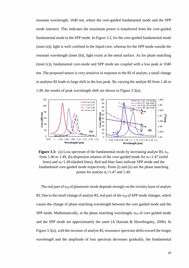
40
resonant wavelength, 1040 nm, where the core-guided fundamental mode and the SPP
mode intersect. This indicates the maximum power is transferred from the core-guided
fundamental mode to the SPP mode. In Figure 3.2, for the core-guided fundamental mode
(inset (a)), light is well confined in the liquid core, whereas for the SPP mode outside the
resonant wavelength (inset (b)), light exists at the metal surface. As for phase matching
(inset (c)), fundamental core-mode and SPP mode are coupled with a loss peak at 1040
nm. The proposed sensor is very sensitive in response to the RI of analyte, a small change
in analytes RI leads to large shift in the loss peak. By varying the analyte RI from 1.46 to
1.49, the results of peak wavelength shift are shown in Figure 3.3(a).
Figure 3.3: (a) Loss spectrum of the fundamental mode by increasing analyte RI, na,
from 1.46 to 1.49, (b) dispersion relation of the core-guided mode for na=1.47 (solid
lines) and na=1.49 (dashed lines). Red and blue lines indicate SPP mode and the
fundamental core-guided mode respectively. Point (i) and (ii) are the phase matching
points for analyte na=1.47 and 1.49.
The real part of neff of plasmonic mode depends strongly on the vicinity layer of analyte
RI. Due to the small change of analyte RI, real part of the neff of SPP mode changes, which
causes the change of phase matching wavelength between the core guided mode and the
SPP mode. Mathematically, at the phase matching wavelength, neff of core guided mode
and the SPP mode are approximately the same (A Hassani & Skorobogatiy, 2006). In
Figure 3.3(a), with the increase of analyte RI, resonance spectrum shifts toward the longer
wavelength and the amplitude of loss spectrum decreases gradually, the fundamental
0
20
40
60
80
100
120
0.97 1 1.03 1.06 1.09 1.12 1.15 1.18 1.21
Lo
ss (
dB
/cm
)
Wavelength (μm)
na=1.46
na=1.47
na=1.48
na=1.49
(a)
1.43
1.435
1.44
1.445
1.45
1.455
1.46
1.465
0
10
20
30
40
50
60
70
80
90
100
1 1.02 1.04 1.06 1.08 1.1 1.12 1.14 1.16 1.18 1.2
Re(
neff)
Lo
ss (
dB
/cm
)
Wavelength (μm)
na=1.47, core modena=1.47, spp modena=1.49, core modena=1.49, spp mode
(i)
(ii)
(b)

41
mode field confinement also increases. The range of resonant wavelength shift is from
1040 to 1070 nm for the change of analyte RI from 1.46 to 1.47. As such, the positive RI
sensitivity is 3000 nm/RIU, which is comparable to (Dash & Jha, 2014b; Gao et al., 2014),
with proposed simpler sensor structure. The sensitivity is determined by following the
equation in (Akowuah et al., 2012); Sensitivity, Sλ(λ)=∆λpeak/∆na, where ∆λpeak is the
resonant peak shift and ∆na is the analyte RI variation. The proposed sensor shows the
sensitivity of 3000, 2900 and 1100 nm/RIU for analyte RI variation range of 1.46-1.47,
1.47-1.48 and 1.48-1.49 respectively.
Generally, PCF SPR sensors show high propagation loss, which limits the sensor’s
length to generate measurable signal (A Hassani & Skorobogatiy, 2006). The propagation
loss of the core guided fundamental mode is a function of analyte RI and the wavelength
which is define as α(λ, na). By considering P0 as the input power launched into the fiber,
the detected power after propagating through the sensor of length L is P(L, λ, na) =
P0exp(−α(λ, na)L). By considering a small change of analyte RI dna, the relative
sensitivity is define as S(λ) = [P(L, λ, na+dna)−P(L, λ, na)]/P(L, λ, na)/dna. Sensor’s length
L could be optimized through the measurement of modal transmission loss. A reasonable
choice for a sensor length is L = 1/α(λ, na), leading to a simple definition of sensitivity
for a small change in analyte RI (Akowuah et al., 2012),
a
a
a
An
n
nRIUS
),(
),(
1])[( 1
(3.1)
In Figure 3.3(b), it is clear that with the increase of analyte RI, phase matching
wavelength changes. Therefore, at the phase matching resonant wavelength, an unknown
sample (analyte) could be detected (Akowuah et al., 2012). As the analyte RI is 1.47, the
resonant wavelength is 1070 nm and the loss is 91 dB/cm whereas for na=1.49, the
resonant wavelength is 1110 nm and the loss is 66 dB/cm. This indicates that with the
increase of analyte RI, energy transfer from the core-guided mode to the SPP mode

42
reduces, at the same time, the resonance spectrum broadens. In addition, by varying the
analyte RI, amplitude of loss peak changes as in Figure 3.4 (amplitude sensitivity).
Amplitude sensitivity decreases gradually with the increase of analyte RI due to the core-
cladding RI contrast. The maximum amplitude sensitivity is 418 RIU-1 at 1070 nm
wavelength for analyte of na=1.46 which is comparable to (Gao et al., 2014; Alireza
Hassani et al., 2008). With this sensitivity, the resolution is 2.4×10⁻⁵ RIU, assuming that
the proposed sensor is able to detect a minimum 1% change of the transmitted light
intensity. Amplitude sensitivity of 410 RIU-1 and 138 RIU-1 are achieved at 1099 nm and
1110 nm for analyte RI of 1.47 and 1.48 respectively. From the wavelength interrogation
and amplitude sensitivity, the proposed sensor is possible to detect high RI liquid in the
form of chemical, biochemical and organic chemical analytes.
Figure 3.4: Amplitude sensitivity as a function of wavelength with the variation of
analyte RI.
Table 3.1 shows the performance comparison of the reported PCF SPR sensors.
-500
-400
-300
-200
-100
0
100
200
0.99 1.02 1.05 1.08 1.11 1.14 1.17 1.2
Am
pli
tud
e S
ensi
tiv
ity
(1
/RIU
)
Wavelength (μm)
na=1.46
na=1.47
na=1.48

43
Table 3.1: Performance analyses of simulated PCF SPR sensors.
Characteristics RI
Range
Interrogation Sensitivity Resolution
(RIU)
Ref.
Multi-hole fiber based SPR
sensor
1.33-1.35 Wavelength 2,000 nm/RIU 5×10⁻⁵ (Gao et
al.,
2014) Amplitude 370 RIU-1 2.7×10⁻⁵
Selectively ITO coated
polymer PCF
1.33-1.35 Wavelength 2,000 nm/RIU 5×10⁻⁵ (Dash
& Jha,
2014b)
Selectively filled silver
nanowires
1.330-
1.335
Wavelength N/A 4.55×10⁻⁵ (Mishr
a,
Mishra,
&
Gupta,
2015)
Amplitude 203 RIU–1 4.9×10⁻⁵
Silver-graphene deposited
core
1.46-1.49 Wavelength 3,000 nm/RIU 3.33×10⁻⁵ (This
work)
Amplitude 418 RIU-1 2.4×10⁻⁵
3.4.2 Performance Analysis and Optimization
The structural parameters of the fiber have huge influence on the sensing performance.
The thickness of the active plasmonic material is important as it has significant effect on
surface plasmon wave excitation. To observe the effect of silver layer thickness on the
performance of sensor, the silver layer thickness is varied for the analyte RI at 1.46 and
1.47 while the other parameters remain constant. The loss spectrum and the amplitude
sensitivity due to the change in silver layer thickness are shown in Figure 3.5. From
Figure 3.5(a), the amplitude of the loss spectrum decreases gradually and shifts toward
the longer wavelength with the increase of silver layer thickness from 35 nm to 45 nm,
this is due to the higher damping loss for thicker silver layer (Lu et al., 2013).

44
Figure 3.5: (a) Loss spectrum and (b) amplitude sensitivity versus wavelength by
varying silver thickness, setting analyte RI at na=1.46.
This indicates that due to the increase of silver thickness, light penetration through the
cladding decreases. The resonance peak shifts are 20, 30 and 40 nm for silver thickness
of 35, 40 and 45 nm respectively. Figure 3.5(b) shows the same scenario, sensitivity
decreases gradually due to the increase of silver thickness. The maximum amplitude
sensitivity is achieved 458, 418 and 380 RIU-1 for silver thickness of 35, 40 and 45 nm
respectively at analyte RI of 1.46. This indicates the inverse relation between the
sensitivity and the silver layer thickness. The increase of silver layer thickness leads to
less penetration of the core mode electric field into the silver layer, resulting in weak
coupling with the surface plasmon modes and subsequently affecting the sensitivity. The
presence of evanescent fields in the silver layer decreases due to the larger thickness. The
amplitude sensitivity of 458, 418 and 380 RIU-1 gives sensor resolution of 2.2×10⁻⁵,
2.4×10⁻⁵ and 2.63×10⁻⁵ respectively by assuming 1% minimum detectable change in the
transmitted light intensity. The thickness of the silver layer is optimized at 40 nm for the
study of the other parameters. This typical mechanism could be useful for the studies of
nanoparticles concentration on the metal surface of a sensor (A Hassani & Skorobogatiy,
2006).
0
20
40
60
80
100
120
140
0.94 0.97 1 1.03 1.06 1.09 1.12 1.15
Loss
(d
B/c
m)
Wavelength (μm)
35nm, na=1.46
35nm, na=1.47
40nm, na=1.46
40nm, na=1.47
45nm, na=1.46
45nm, na=1.47
-600
-500
-400
-300
-200
-100
0
100
200
0.97 1 1.03 1.06 1.09 1.12
Am
pli
tud
e S
ensi
tivit
y (
1/R
IU)
Wavelength (μm)
35 nm
40 nm
45 nm
(a) (b)
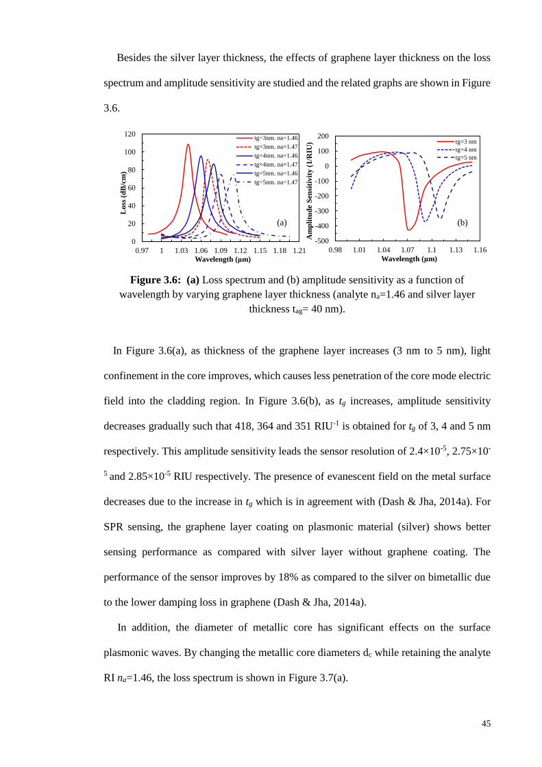
45
Besides the silver layer thickness, the effects of graphene layer thickness on the loss
spectrum and amplitude sensitivity are studied and the related graphs are shown in Figure
3.6.
Figure 3.6: (a) Loss spectrum and (b) amplitude sensitivity as a function of
wavelength by varying graphene layer thickness (analyte na=1.46 and silver layer
thickness tag= 40 nm).
In Figure 3.6(a), as thickness of the graphene layer increases (3 nm to 5 nm), light
confinement in the core improves, which causes less penetration of the core mode electric
field into the cladding region. In Figure 3.6(b), as tg increases, amplitude sensitivity
decreases gradually such that 418, 364 and 351 RIU-1 is obtained for tg of 3, 4 and 5 nm
respectively. This amplitude sensitivity leads the sensor resolution of 2.4×10⁻⁵, 2.75×10-
5 and 2.85×10⁻⁵ RIU respectively. The presence of evanescent field on the metal surface
decreases due to the increase in tg which is in agreement with (Dash & Jha, 2014a). For
SPR sensing, the graphene layer coating on plasmonic material (silver) shows better
sensing performance as compared with silver layer without graphene coating. The
performance of the sensor improves by 18% as compared to the silver on bimetallic due
to the lower damping loss in graphene (Dash & Jha, 2014a).
In addition, the diameter of metallic core has significant effects on the surface
plasmonic waves. By changing the metallic core diameters dc while retaining the analyte
RI na=1.46, the loss spectrum is shown in Figure 3.7(a).
-500
-400
-300
-200
-100
0
100
200
0.98 1.01 1.04 1.07 1.1 1.13 1.16
Am
pli
tud
e S
ensi
tiv
ity (
1/R
IU)
Wavelength (μm)
tg=3 nm
tg=4 nm
tg=5 nm
0
20
40
60
80
100
120
0.97 1 1.03 1.06 1.09 1.12 1.15 1.18 1.21
Loss
(d
B/c
m)
Wavelength (μm)
tg=3nm. na=1.46
tg=3nm. na=1.47
tg=4nm. na=1.46
tg=4nm. na=1.47
tg=5nm. na=1.46
tg=5nm. na=1.47
(a) (b)
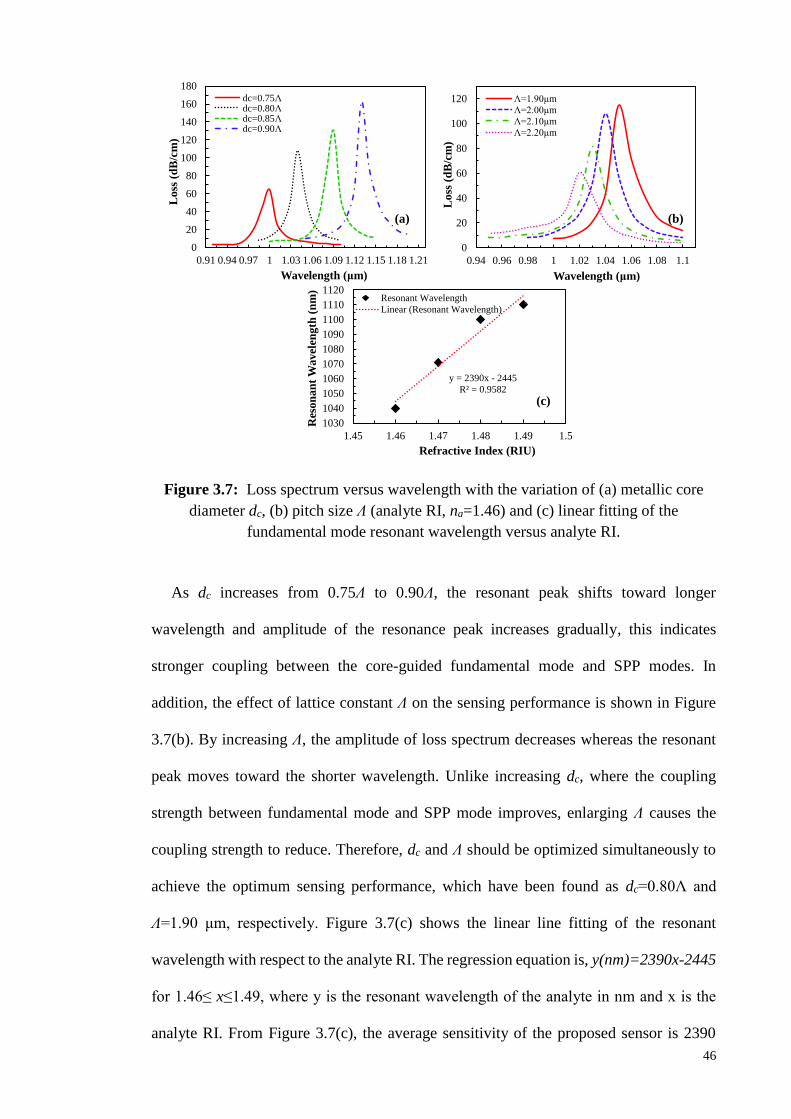
46
Figure 3.7: Loss spectrum versus wavelength with the variation of (a) metallic core
diameter dc, (b) pitch size Λ (analyte RI, na=1.46) and (c) linear fitting of the
fundamental mode resonant wavelength versus analyte RI.
As dc increases from 0.75Λ to 0.90Λ, the resonant peak shifts toward longer
wavelength and amplitude of the resonance peak increases gradually, this indicates
stronger coupling between the core-guided fundamental mode and SPP modes. In
addition, the effect of lattice constant Λ on the sensing performance is shown in Figure
3.7(b). By increasing Λ, the amplitude of loss spectrum decreases whereas the resonant
peak moves toward the shorter wavelength. Unlike increasing dc, where the coupling
strength between fundamental mode and SPP mode improves, enlarging Λ causes the
coupling strength to reduce. Therefore, dc and Λ should be optimized simultaneously to
achieve the optimum sensing performance, which have been found as dc=0.80Λ and
Λ=1.90 μm, respectively. Figure 3.7(c) shows the linear line fitting of the resonant
wavelength with respect to the analyte RI. The regression equation is, y(nm)=2390x-2445
for 1.46≤ x≤1.49, where y is the resonant wavelength of the analyte in nm and x is the
analyte RI. From Figure 3.7(c), the average sensitivity of the proposed sensor is 2390
0
20
40
60
80
100
120
0.94 0.96 0.98 1 1.02 1.04 1.06 1.08 1.1
Lo
ss (
dB
/cm
)
Wavelength (μm)
Λ=1.90μm
Λ=2.00μm
Λ=2.10μm
Λ=2.20μm
(b)
y = 2390x - 2445
R² = 0.9582
1030
1040
1050
1060
1070
1080
1090
1100
1110
1120
1.45 1.46 1.47 1.48 1.49 1.5
Res
on
an
t W
av
elen
gth
(n
m)
Refractive Index (RIU)
Resonant Wavelength
Linear (Resonant Wavelength)
(c)
0
20
40
60
80
100
120
140
160
180
0.91 0.94 0.97 1 1.03 1.06 1.09 1.12 1.15 1.18 1.21
Lo
ss (
dB
/cm
)
Wavelength (μm)
dc=0.75Λdc=0.80Λdc=0.85Λdc=0.90Λ
(a)
47
nm.RIU-1 and R2 value is 0.9582, indicating good fitting of the sensor response. The
obtained result is comparable with the results reported in (Yu et al., 2010). Owing to the
high sensitivity and linearity, the sensor could be implemented as a standardized sensor
for high RI analytes detection.
3.5 Summary
In this chapter, numerically investigate a PCF based SPR sensor where the core was
deposited with graphene-silver. Graphene layer is used to inhibit oxidation of the active
plasmonic material, silver. The metallic channel hole and the fiber cores are infiltrated
with the sample, high RI liquid analyte. As the liquid-filled cores satisfy the optimum RI
and dispersion relation simultaneously, SPR sensing performance is increased
significantly. Amplitude sensitivity as high as 418 RIU-1 has been demonstrated, which
gives sensor resolution of 2.4×10⁻⁵ RIU, assuming that the sensor is able to detect a
minimum 1% change of the transmitted intensity. The proposed senor shows maximum
RI sensitivity of 3000 nm/RIU with sensor resolution of 3.33×10⁻⁵ RIU, whereas the
average RI sensitivity is 2390 nm/RIU in the sensing range of 1.46 to 1.49. Due to the
promising results, the proposed sensor could be a potential candidate for detecting
chemical, organic-chemical, and other analytes.

48
CHAPTER 4: FLAT FIBER BASED PLASMONIC SENSOR
4.1 Introduction
In this chapter, a simple liquid analyte filled multi-core flat fiber (MCFF) based
Surface Plasmon Resonance (SPR) refractive index sensor operating in
telecommunication wavelengths is proposed for refractive index sensing. Chemically
stable gold (Au) and titanium dioxide (TiO2) layers are used at external surface of the
fiber structure to realize a simpler detection mechanism. Sensor performance is
investigated by wavelength interrogation method and amplitude interrogation method.
4.2 Technical Review
Optical fibers are the natural candidate for distributed or remote optical sensing as
they are mechanically flexible, immune to electromagnetic interference (EMI), low loss
in telecom wavelengths and can be fabricated over kilometer-lengths. On the other hand,
planar light wave circuits offer multifunctionality with the capability to sense multiple
substances on a single platform. Flat optical fiber is a hybrid format of waveguide that
combines the advantages of conventional optical fiber with the multifunctionality of
planar waveguides (Adikan et al., 2012; Holmes et al., 2008). Recently, Egorova et al.
(2014) and Mahdiraji et al. (2014) fabricated a new class of flat fiber called as Multi-Core
Flat Fiber (MCFF), which opens a new window for designing more versatile photonic
sensors due to having larger and flat surface functionality and flexibility in employing
multiple waveguide channels with similar or different operating wavelengths. In this
study, a novel, highly sensitive MCFF structure based SPR sensor is numerically
demonstrated. Metallic layer and sensing layer are placed outside the fiber structure
which made the proposed sensor simpler in terms of fabrication. The proposed sensor can
be fabricated by following the MCFF method (Ghafour Amouzad Mahdiraji, 2015; G
Amouzad Mahdiraji et al., 2014; Mahdiraji et al., 2014) and thin layer deposition

49
sputtering method (Malinský et al., 2012). Besides, selective liquid infiltration of holes
in PCF can be done by selectively closing the holes using two-photon direct laser writing
(Vieweg et al., 2010) and direct gluing method (Kuhlmey, Eggleton, & Wu, 2009). The
detection of analyte can be carried out simply by flowing it through or dripped on the
outer surface of metal layer. The proposed sensor can be calibrated with a liquid with
known RI, using the flow cell analyte containing process. The effect of sensor structural
parameters such as gold thickness, titanium dioxide thickness and core diameter on the
plasmonic excitation is analyzed and optimized for the sensing performance as well as
reducing the sensor footprint.
4.3 MCFF SPR Sensor Design and Theoretical Modeling
Figure 4.1: (a) Schematic of the proposed MCFF in 3D model, (b) cross-section of 2D
computational model of MCFF SPR sensor, (c) Analyte flow through sensing layer:
Ligands attached with TiO2 layer, (d) Sensing response curve: reference peak (without
analyte presence), shift right (red) or left (blue) with the presence of analytes.
Figure 4.1(a) shows the schematic of the proposed MCFF where the identical liquid
cores and air-holes are arranged in a line. In principle, the number of liquid cores and air
holes are scalable for desirable sensing application and is mainly limited by the fiber
drawing technology. To simplify the fabrication process, gold layer, titanium dioxide
layer and sensing layer are arranged sequentially on top of the MCFF surface, as shown
Wavelength
Sen
sin
g R
esp
on
se
ReferenceRed shiftBlue Shift
(d)
(c)
Analyte
Ligand
Sensing Layer
TiO2 Layer
Gold Layer
(b)
dc dΛ
Sensing Layer
TiO2 Layer
Gold Layer
Liquid Analyte
Air
Fused Silica
(a) (c)

50
in Figure 4.1(b). Figure 4.1(c) is a conceptual diagram where analyte will flow through
the sensing medium and bond with the ligands, resulting the shift in resonance peak. Due
to the presence of analyte, resonance peak can be either blue or red shifted as shown in
Figure 4.1(d). A higher refractive index liquid analyte (varies RI from 1.460 to 1.485) is
used in the cores compare to the silica (SiO2) to allow the total internal reflection (TIR)
guiding mechanism. The proposed sensor has a pitch size of Λ=1.20 µm, core diameter
dc=1.20 µm and the air hole diameter is d=1 µm. Generally, Gold (Au) and silver (Ag)
are widely used for the plasmonic applications due to their relatively low loss in the
visible and near-infrared region (NIR) (West et al., 2010). Although, silver has low loss
in the visible range, it is chemically unstable and it oxidizes easily. Gold is used as the
active plasmonic material which is chemically stable and also having the higher
resonance shift capability (Dash & Jha, 2014a). On top of the gold layer, a thin transparent
high refractive index TiO2 layer is deposited. The presence of TiO2 layer will enhance the
interaction of evanescent field with the analyte layer and shifted the resonant wavelengths
towards the near-infrared wavelengths. Recently, Di Gao et al. reported the multi-hole
based SPR sensor with the TiO2 layer to operate the sensor at near-infrared region (2014).
Gold layer is used outside the cladding with the fixed thickness t=40 nm and a TiO2 layer
above the gold layer with thickness tt = 80 nm. Sequentially, sensing layer is on top of
the TiO2 surface. The refractive index of the fused silica can be obtained by following the
Eq. 2.26. The dielectric constant of gold is defined by the Drude-Lorentz model (Vial et
al., 2005) and the equation is written as:
LL
L
D
DAu
jj
)(
.
)( 22
22
(4.1)
where εAu is the permittivity of dielectric material, gold, ε∞ is the permittivity at high
frequency and its value is 5.9673. The angular frequency can be expressed as ω = 2πC/λ,
C is the velocity of light in vacuum. Moreover, ωD and γD are the plasma frequency and

51
damping frequency respectively, whereas ΩD/2π = 2113.6 THz and γD/2π = 15.92 THz.
Weighting factor is expressed as ∆ε = 1.09 while, ΓL/2π = 104.86 THz and ΩL/2π = 650.07
THz are the spectral width and oscillator strength respectively of the Lorentz oscillators.
The refractive index profile of TiO2 is calculated by the following equation (DeVore,
1951).
)10803.0(
10441.2913.5
72
72
n (4.2)
Finite-element method based commercial COMSOL software is used to investigate
the guiding properties and sensing performance. Outside the structure, PML and
scattering boundary conditions are sequentially used to absorb the radiated light towards
the surface.
4.4 Results and Discussions of the MCFF-SPR Sensor
MCFF SPR sensors are worked based on the evanescent field which is produced due
to light propagation through the core. The core-clad arrangement in a line leads to leakage
of light that produces more evanescent field. By keeping the metallic layer close to the
cores which help to excite the free electrons of the metal layer easily to introduce the
surface plasmon. At a certain wavelength, real effective index value of core-guided mode
and real neff of surface plasmon polaritons mode is equal, this wavelength is called the
resonant wavelength. At the resonant wavelength, evanescent field can easily excite the
free electrons of metal surface, resulting the generation of surface plasmon waves. The
proposed design shows the two fundamental modes (x- and y-component modes), in this
work y-component fundamental mode is analyzed to investigate the propagation loss. The
x-component fundamental mode shows the same resonance peak similar to y-component
but with lower loss depth. The fundamental core guided mode, SPP mode and the
resonant spectrum at analyte refractive index na = 1.46 is shown in Figure 4.2.

52
Figure 4.2: Dispersion relations of the plasmonic mode (red) and fundamental core
mode (green), and loss spectrum (blue) with the structural parameters: dc = 1.20 μm, d =
1 μm, t = 40 nm, tt = 80 nm.
The real part of neff of the core guided mode and the SPP mode are presented by the
green and red solid line respectively. The effective index of the core-guided fundamental
mode (green) and SPP mode (red) coincide at resonant wavelength 1.345 μm, where a
sharp loss peak is found. This indicates the maximum energy transfer from the core-
guided fundamental mode to the SPP mode. By using the imaginary part of neff, the
propagation loss is defined by the following equation (Akowuah et al., 2012).
α = 40π.Im(neff) / (ln(10)λ)≈ 8.686 × k0.Im[neff]×104 dB/cm (4.3)
where k0=2π/ is the wave number in the free space and the wavelength, λ is in μm.
It is clearly visible from inset(a) that at the core guided fundamental mode, the electric
field is well confined in the liquid core and the SPP mode, and from inset (b), the electric
field is introduced on the metal surface outside the resonant wavelength. In inset (c), the
fundamental core mode and SPP mode are phase matched at a given wavelength 1.345
μm. At this wavelength, the fundamental mode and the SPP mode are coupled together.
A sharp loss peak appears at phase matching wavelength, providing a signature for
detection of the analyte. The performance of proposed sensor is evaluated in terms of
sensitivity, accuracy, linearity and resolution. The proposed sensor is very sensitive due
plasmon
1.355
1.36
1.365
1.37
1.375
1.38
1.385
100
200
300
400
500
600
700
1.24 1.26 1.28 1.3 1.32 1.34 1.36 1.38 1.4 1.42
Rea
l(nef
f) (
RIU
)
Lo
ss (
dB
/cm
)
Wavelength (µm)
na=1.46, core mode
na=1.46, core mode
na=1.46, spp mode
(a)(c)
(a)
(b)
(b)
(c)

53
to small change of analyte. The small change of analyte RI induces a significant shift of
loss peak. Figure 4.3 shows the response of the sensor for analyte RI from 1.46 to 1.485.
Figure 4.3: (a) Loss spectra of the fundamental mode with analyte RI na varied from
1.46 1.485, (b) linear fitting of the fundamental mode resonant wavelength vs. analyte
RI.
The real part of neff of plasmonic mode depends strongly on the vicinity layer of analyte
RI. Due to the small change of analyte RI, real part of the neff of SPP mode changes, which
causes the change of phase matching wavelength between the cores guided mode and the
SPP mode. As depicted in Figure 4.3(a), by increasing the analyte RI, the loss peak shifts
toward the shorter wavelengths, which is in agreement with the works reported in (Qin et
al., 2014; Shuai, Xia, & Liu, 2012). The increase of analyte RI shifts the Real(neff) of the
SPP curve in Figure 4.2 (inset (c)) towards higher value collectively. As a result, the phase
matching wavelength or resonance peak is shifted towards the lower wavelength. By
varying the analyte RI with an iteration of 0.005, resonance wavelength shifts are 15, 25,
115, 50 and 35 nm, respectively towards the lower wavelength, as shown in Table 4.1.
The highest sensitivity is observed within the analyte RI of 1.47 to 1.475, which provides
the maximum loss peak shift 115 nm, i.e., from 1.305 to 1.190 μm. Moreover, the
maximum loss peak value 818 dB/cm is achieved at 1.305 μm wavelength and the
minimum loss peak value is achieved 695 dB/cm at 1.190 μm wavelength while the
analyte RI are 1.47 and 1.475, respectively. Generally, microstructured optical fiber based
SPR sensors show high propagation loss, as a result, it limits the sensor length to generate
R² = 0.9432
1.05
1.1
1.15
1.2
1.25
1.3
1.35
1.4
1.455 1.465 1.475 1.485
Res
on
ant
Wav
elen
gth
(μ
m)
Refractive Index (RIU)
Resonant Wavelength
linear fit of Res. Wave.
30
130
230
330
430
530
630
730
830
930
1 1.05 1.1 1.15 1.2 1.25 1.3 1.35 1.4 1.45 1.5
Lo
ss (
dB
/cm
)
Wavelength (µm)
na=1.460na=1.465na=1.470na=1.475na=1.480na=1.485
(a)(b)
115 nm

54
the measurable signal to detect the unknown analytes (A Hassani & Skorobogatiy, 2006).
The sensitivity of the proposed sensor is analyzed by using the wavelength interrogation
and amplitude interrogation method. The sensitivity of wavelength interrogation is
measured by the following equation (Alireza Hassani et al., 2008),
Sensitivity, Sλ [nm/RIU] = ∆λpeak / ∆na (4.4)
where ∆λpeak is the resonance peak shift and ∆na is the variation of the analyte refractive
index.
The proposed MCFF sensor shows the maximum sensitivity of 23000 nm/RIU, at the
analyte RI of 1.47 and the average sensitivity of the sensor is 9600 nm/RIU. The
resonance peaks are found at 1.345, 1.330, 1.305, 1.190, 1.140 and 1.105 μm wavelength
where the full-width-at-half-maximum (FWHM) values are 36, 43, 54, 46, 41 and 29 nm
for the analyte refractive index 1.46, 1.465, 1.47, 1.475, 1.48 and 1.485, respectively, as
shown in Table 4.1. Besides, detection accuracy of a sensor is the reciprocal of FWHM,
i.e. Dn=1/FWHM (Dash & Jha, 2015a). Therefore, lower FWHM values means the
sharper resonance curve resulting the higher detection accuracy. Furthermore, as depicted
in Figure 4.3(b), the proposed sensor shows the linearity R2 value of 0.9432 in the sensing
range of 1.46 to 1.485, which indicates the high linear sensing response. Assuming the
minimum spectral resolution of ∆λmin = 0.1 nm and considering the maximum peak shift
∆λpeak = 115 nm, which is obtained based on the analyte RI variation of ∆na = 0.005, as
shown in Figure 4.3(a), the RI resolution can be calculated as following equation (Gao et
al., 2014).
R = ∆na × ∆λmin / ∆λpeak RIU (4.5)
The resolution of the proposed sensor is as high as 4.35×10⁻⁶ RIU, which indicates
capability of the sensor in detecting very small RI changes in the order of 10-6. The
resolution of the proposed sensor is better compared to the results reported in (Dash &
Jha, 2014b; Shuai, Xia, & Liu, 2012).

55
Table 4.1: Performance analysis with the variation of analyte RI.
Analyte
RI
Resonance
peak
wavelength
(μm)
Resonance
peak shift
(nm)
Sensitivity
[nm/RIU]
FWHM
(nm)
1.460 1.345 15 3000 36
1.465 1.330 25 5000 43
1.470 1.305 115 23000 54
1.475 1.190 50 10000 46
1.480 1.140 35 7000 41
1.485 1.105 - - 29
The performance comparisons of the proposed sensor against the previously reported
SPR sensors are presented in Table 4.2.
Table 4.2: Performance comparison of simulated SPR sensors.
Structural configuration of
RI sensor
Wave.
interrogation
sensitivity,
nm/RIU
Amp.
Sens.,
RIU-1
Resolution
(using wav.
inter.), RIU
Ref.
Bragg fiber based SPR
sensor
1,2000 269 8.3 × 10⁻⁶ (Alireza
Hassani et al.,
2008)
Hollow core D-shaped PCF
SPR sensor
6,430 N/A N/A (Tan et al.,
2014)
Liquid core PCF based SPR
sensor
-5,000;
3,700
N/A 2.7 × 10⁻⁶ (Shuai,
Xia, & Liu,
2012)
Solid core D-shaped PCF
SPR sensor
7300 N/A N/A (Tian et al.,
2012)
Graphene based PCF based
SPR sensor
N/A 860 N/A (Dash &
Jha, 2014a)
Solid core honeycomb PCF
SPR sensor
13,750 400 N/A (Gauvreau
et al., 2007)
Exposed-core grapefruit
fiber
13,500 N/A N/A (Rhodes et
al., 2008)
MCFF based SPR sensor 23,000
820 4.35×10⁻⁶ (This
work)

56
The thickness of the gold layer is influential on the sensing performance as well. The
effect of analyte RI and gold thickness changes on the loss spectrums are shown in Figure
4.4. Figure 4.4 shows the blue shift of the loss spectrum with the increase of gold layer
thickness. At thickness of t=40 nm, the maximum losses of 697 dB/cm and 723 dB/cm
are achieved at resonant wavelength 1.345 μm and 1.330 μm due to analyte RI of 1.460
and 1.465, respectively. The variation in Au layer thickness will affect the real neff of the
surface plasmon mode, thus causing the shift in phase matching wavelength. Au layer
thickness will affect the real neff of the surface plasmon mode, thus causing the shift in
phase matching wavelength. In addition, it is visible that the loss depth of the sensor is
decreased with thicker Au layer as indicated in Figure 4.4. This is because as the thickness
of Au layer is increased, the penetration of evanescent field towards the surface is less.
The variation in loss depth is a critical issue as it will affect the sensitivity of the sensor
in amplitude interrogation mode. Practically, the thickness of the Au layer should be
determined specifically for optimum sensing performance in wavelength or amplitude
interrogation.
Figure 4.4: Loss spectrum of wavelength with the variation of gold thickness t from
35-50 nm, by setting na=1.46, dc=1.20 μm and tt=80 nm.
Besides the gold layer thickness, effects of TiO2 layer thickness on sensing
performance are investigated. TiO2 attracts the core-guided evanescent fields towards the
surface and help to facilitate the interaction between the core-guided mode and the SPP
80
180
280
380
480
580
680
780
1.27 1.29 1.31 1.33 1.35 1.37 1.39 1.41
Loss
(dB
/cm
)
Wavelength (μm)
na=1.460, t=35 nmna=1.465, t=35 nmna=1.460, t=40 nmna=1.465, t=40 nmna=1.460, t=45 nmna=1.465, t=45 nmna=1.460, t=50 nmna=1.465, t=50 nm

57
mode. Due to its high refractive index, it turns the sensor operation in near-infrared region
(Gao et al., 2014). The effect of loss spectra due to variation of TiO2 thickness from 70
to 85 nm are shown in Figure 4.5(a).
Figure 4.5: Loss spectrum analysis with varying the (a) TiO2 thickness, and (2) liquid
core-diameter (dc); setting na= 1.46, d= 1 μm, and tg= 40 nm.
It is clearly observed that the loss peaks appear at 1.345 μm wavelength and the loss
depths are increase slightly with the increment in TiO2 thickness. The minimum loss
value 649 dB/cm is achieved while the TiO2 thickness is 70 nm and it increased to the
maximum loss value of 697 dB/cm at the thickness of 85 nm. Due to increase of TiO2
thickness, evanescent field is attracted towards the surface and interacts strongly with the
analytes, thereby, the loss depths are gradually increased. The core diameter effects on
the sensing performance also considered, as shown in Figure 4.5(b). Due to change of
liquid-filled core diameter dc from 1.15 to 1.30 μm, resonance peaks are found to be
around 1.345 μm with very small shift toward the lower wavelength and slightly gaining
in the resonance depths. At the core-diameter 1.15 μm, loss value 660 dB/cm is achieved,
while it is dramatically increased to 753 dB/cm when the dc is increased to 1.30 μm. This
indicates the stronger coupling between the core-guided fundamental mode and SPP
mode with the increase of dc.
Furthermore, the performance of the sensor is evaluated by the mean of amplitude
detection method. Spectral manipulation is not necessary in this method as all the
measurement operations are done in a specific wavelength (Gauvreau et al., 2007). The
100
200
300
400
500
600
700
800
1.24 1.26 1.28 1.3 1.32 1.34 1.36 1.38 1.4
Lo
ss (
dB
/cm
)
Wavelength (µm)
dc=1.15 µm
dc=1.20 µm
dc=1.25 µm
dc=1.30 µm
550
650
750
1.335 1.343 1.351
180
260
340
420
500
580
660
740
1.295 1.31 1.325 1.34 1.355 1.37 1.385
Lo
ss (
dB
/cm
)
Wavelength (µm)
dt=70 nmdt=75 nmdt=80 nmdt=85 nm
550
600
650
700
1.34 1.344 1.348
(a) (b)

58
effect of analyte RI and gold thickness variation on amplitude sensitivity is shown in
Figure 4.6(a) and (b), respectively, considering the optimum core diameter of dc=1.20
μm. The amplitude sensitivity can be calculated by following the Eq. 3.1.
Figure 4.6: Dependence of the sensor amplitude sensitivity (a) with the variation of
analyte RI; (b) with the variation of gold thickness at analyte RI, na=1.460.
As shown in Figure 4.6(a), the maximum amplitude sensitivity of 820 RIU-1 is
obtained at 1140 nm wavelength for the analyte RI na=1.475. The proposed amplitude
sensitivity result is comparable with the results reported in (Gao et al., 2014; Alireza
Hassani et al., 2008). The proposed sensor resolution 1.22×10⁻⁵ RIU is achieved
(considering amplitude sensitivity 820 RIU-1), by assuming the minimum 1% change of
the transmitted intensity is detectable. Amplitude sensitivities of 196, 233, 590 and 534
RIU-1 are achieved for the other analyte RI of 1.46, 1.465, 1.47 and 1.48, respectively.
The amplitude sensitivity is found to be inversely proportional to the gold thickness as
depicted in Figure 4.6(b). The maximum amplitude sensitivity achieved is 202 RIU-1 at
1.330 μm for the gold thickness of 35 nm. This implies the sensing resolution of 4.95×10-
5 RIU with the same assumption of 1% change of the transmitted intensity. Moreover,
amplitude sensitivity of 196, 190 and 181 RIU-1 are achieved with the gold thicknesses
of 40, 45 and 50 nm, respectively. By increasing the gold thickness, sensitivity is
decreased significantly, due to the higher damping loss for the thicker gold layer. Owing
to the high wavelength sensitivity, amplitude sensitivity and high sensor resolution, the
-300
-100
100
300
500
700
900
1.04 1.08 1.12 1.16 1.2 1.24 1.28 1.32 1.36 1.4
Am
pli
tude
Sen
siti
vit
y (
1/R
IU)
Wavelength (µm)
na=1.460na=1.465na=1.470na=1.475na=1.480
(a) (b)
-150
-70
10
90
170
250
1.27 1.29 1.31 1.33 1.35 1.37 1.39
Am
pli
tude
Sen
siti
vit
y (
1/R
IU)
Wavelength (μm)
t=35 nm
t=40 nm
t=45 nm
t=50 nm

59
proposed sensor could be implemented as a standardized sensor for the high RI analytes
detection.
4.5 Summary
A simple multi-core flat fiber structure based surface plasmon resonance sensor is
demonstrated for the first time. The proposed sensor shows a sensitivity as high as 23,000
nm/RIU, which is highest among the reported microstructured SPR sensors. As the liquid-
filled cores satisfy the optimum index and dispersion property simultaneously, the SPR
sensing performance is increased significantly. The proposed sensor shows the average
sensitivity of 9,600 nm/RIU, at the sensing RI range of 1.46-1.485. The proposed sensor
shows high sensing resolution as high as ~4.35×10⁻⁶ RIU. Additionally, the proposed
sensor offers a maximum amplitude sensitivity and sensor resolution of 820 RIU-1 and
1.22×10⁻⁵ RIU, respectively. The results demonstrate the feasibility of MCFF based SPR
sensor towards the possibility of integrated SPR sensor-on-a-chip. Multiple cores along
the MCFF could enable a real time monitoring of different physical and biological
analytes.

60
CHAPTER 5: PCF SPR WITH EXTERNAL SENSING
APPROACH
5.1 Introduction
In this chapter, a simple, two rings, hexagonal lattice PCF biosensor using Surface
Plasmon Resonance phenomenon is proposed. An active plasmonic gold layer and the
analyte are placed outside the fiber structure instead of inside the air-holes, which will
result in a simpler and straight forward fabrication process. The proposed sensor exhibits
birefringent behavior that enhances its sensitivity. Numerical investigation of the guiding
properties and sensing performance are conducted by FEM. Finally, fabrication tolerance
is shown to make the sensor feasible.
5.2 Technical Review
Recently, by integrating the SPR phenomenon, PCF has shown great potential for
biosensing due to its special characteristics, such as small size and design flexibility
(Dash & Jha, 2014a). By modifying the structure and dimension of PCF, it is possible to
increase the evanescent field and manipulate the modal characteristics of the propagating
light. To enhance the sensitivity and realize the narrow resonance peak, single mode light
propagation is more suitable (Shuai, Xia, Zhang, & Liu, 2012). Recently, multi-hole fiber
based SPR sensor was proposed by Gao et al. (2014), where all the holes were coated
with gold and titanium dioxide. To realize the multi-analytes detection, Akowuah et al.
proposed the elliptical air-hole PCF-SPR sensor with four micro fluidic slots (2012).
Besides, high refractive index (RI) analytes, selectively gold coated with analyte-filled
core had been proposed by Qin et al. (2014). In such PCF based SPR sensors where metal
layer need to be coated inside the fiber-holes; one of the major challenge is to achieve
uniform coating inside the micrometer diameter capillary holes. Additional drawback is

61
that the liquid has to be selectively infiltrated into the fiber holes, which limits its practical
implementation. To eliminate these practical challenges and limitations, recently, several
PCF based SPR sensors are reported where the metal coating and the sensing layers are
applied on the outer surface of the fiber structure. Tan et al. (2014) proposed a D-shape
PCF providing a flat outer surface for the metal and sensing layers, however, this requires
accurate polishing effort to precisely remove a predetermined portion of the PCF. In other
studies, proposed two irregular PCF structures where the SPR sensing layer is placed at
the outer surface of the fiber (Dash & Jha, 2014a). Fabrication of such irregular PCF
structures that requires different sizes of holes to be placed in specific positions in the
fiber geometry, which is practically challenging even with very accurate fiber preform
drilling systems.
In this chapter, a simple PCF biosensor based on SPR is proposed. Since the sensing
layers of the proposed sensor are located at outside of the PCF, detection of the unknown
analyte can be carried out simply by flowing it through or dripped on the outer surface of
metal layer. Gold is used as the plasmonic material since it is chemically stable in aqueous
environment and shows high resonance peak shift (Dash & Jha, 2014a). The proposed
sensor in this work could be fabricated easily using standard stack-and-draw PCF drawing
method (G Amouzad Mahdiraji et al., 2014) and sputter deposition method (Malinský et
al., 2012). In addition, the effect of gold layer for plasmonic excitation are investigated
and optimized for the sensing performance, as well as reducing the sensor footprint.
5.3 Structural Design and Theoretical Modelling
Figure 5.1(a) shows the cross-section of the proposed PCF preform structure based on
the stacking of different capillaries (G Amouzad Mahdiraji et al., 2014). Figure 5.1(b)
shows the cross-section of the proposed sensor. Here, propose a two-ring, hexagonal
lattice PCF with a small central air hole which facilitates phase matching between the
core-guided fundamental mode and the surface plasmon polaritons mode. Two holes in

62
the first ring next to the central hole are omitted to introduce birefringence effect. Two
air-holes in the second ring at the same row with the central air-hole are scaled down to
concentrate the evanescent field at two opposite sides of the fiber so that the surface
plasmon could be excited efficiently. The proposed PCF structure can be fabricated by
introducing solid rods and capillaries with thicker wall, as shown in Figure 6.1(a).
Figure 5.1: Cross-section of the proposed (a) PCF’s stacked preform, (b) sensor.
All the air-holes are in circular shape. As shown in Figure 5.1(b), air-holes diameters are
dc = 0.15Λ, d1 = 0.25Λ and d = 0.5Λ. Hole-to-hole distance (pitch size) is Λ = 2 μm. The
refractive index of fused silica used in the modeling follows the Sellmeier equation
(Akowuah et al., 2012). At the outer surface of the fiber structure, a thin gold layer with
a fixed thickness (dg= 40 nm) is used as the plasmonic material. This kind of thin layer
can be integrated outside the fiber structured by using sputtering technique, high pressure
CVD technique, etc. (Malinský et al., 2012; Sazio et al., 2006). The dielectric constant of
gold is defined by Drude-Lorentz model (Vial et al., 2005). On top of the gold layer is
the sample (analyte), which is defined as a dielectric layer. The performance of the
proposed sensor is numerically studied using FEM based commercial COMSOL software
with a circular PML, which prevents reflection by absorbing the scattered light from the
structure.
Solid Road
Capillary
xy
(a) (b)
Fused Silica
Air
Gold
Liquid
PML Layer
dcd1
d
Ʌ

63
5.4 Results and Performance Analysis
The working principle of the PCF-SPR sensors is based on the interaction of
evanescent field with the metal layer. Light propagating in the core produces evanescent
field that penetrates through the cladding region. At a resonant wavelength, real part of
the core guided effective refractive index and the surface plasmon effective refractive
index are equal. The core-clad evanescent field excites the free electrons of the metal
surface, as a result, surface plasmon wave is generated. A sharp loss peak appears at the
resonant wavelength and the RI of the unknown analyte could be detected via wavelength
shift or amplitude variations of this peak. Due to the birefringence, the proposed sensor
shows two fundamental modes. As depicted in Figure 5.2(a), y-component shows higher
effective index profile as compared to x-component. Moreover, the proposed sensor
shows higher fundamental mode resonance loss peak using the y-component as compared
to the x-component mode. In the following work, y-component fundamental mode is
considered. The proposed sensor’s electric field profile and phase matching property are
shown in Figure 5.2 with analyte RI, na=1.36.
1.44
1.445
1.45
1.455
1.46
1.465
0
10
20
30
40
50
480 520 560 600 640 680 720 760 800
Eff
ecti
ve
Ind
ex (
Rea
l)
Lo
ss (
dB
/cm
)
Wavelength (nm)
y-pol core mode
x-pol core mode
y-pol core mode
y-pol spp mode
x-pol core mode
(a)

64
Figure 5.2: Field profile of the proposed sensor at analyte RI 1.36, (a) dispersion
relations of fundamental mode and SPP mode; (b) and (d) x-component fundamental
core guided mode and SPP mode, respectively, (c) and (e) y-component fundamental
core guided mode and SPP mode, respectively.
Figure 5.2(b) and (c) show the core-guided fundamental mode for x-component and y-
component, respectively. When the light is propagating through the core, y-component
light is refracted towards the surface compared to the x-component light. It is clearly
visible that the y-component electric field is stronger in the sensing layer as compared
with the x-component. The intensity of electric field on the metal surface indicates the
sensitivity level. Figure 5.2(d) and (e) show the SPP mode for x-component and y-
component, respectively. Additionally, Figure 5.2(a) shows the phase matching at 670
nm where the effective index of the core-guided fundamental mode and SPP mode
coincide for the analyte with RI 1.36. At the resonant peak of 670 nm, largest energy is
transferred from core-guided fundamental mode to SPP mode, when both modes are
strongly coupled. The phase matching coupling phenomenon is verified by the
coincidence of the resonant peak and the intersection between the dispersion relations of
the core-guided mode and SPP mode. The confinement loss is calculated by Eq. 4.3.
The real part of the surface plasmon mode effective index is strongly influenced by
the analyte refractive index. This in turn determines the wavelength for the phase
matching condition between the core guided mode and surface plasmon polaritons modes.
Figure 5.3 shows the peak wavelength shift resulted by varying the analyte RI from 1.33
to 1.37. The increase of analyte RI will shift the Real(neff) of the SPP curve shown in
Figure 5.2(a) towards higher value collectively.
(b) (c) (d) (e)

65
Figure 5.3: Fundamental loss spectrums by varying the analyte RI from 1.33 to 1.37
(dc=0.15Λ, d1=0.25Λ, d=0.5Λ and tg=40 nm).
As a result, the phase matching wavelength or resonance peak is shifted towards the
longer wavelength. By increasing the analyte RI, resonance peak shifts toward the longer
wavelength and the loss depth is increased simultaneously due to the lower core-cladding
index contrast. Lower resonant depth was observed with analyte of RI at 1.33. This
indicates weaker energy transfer from the core guided mode to the SPP mode, which
results in the broadening of resonant spectrum (Shuai, Xia, & Liu, 2012). Using
wavelength interrogation method, the proposed sensor shows maximum positive
sensitivity of 4000 nm/RIU and the sensing resolution is 2.5×10⁻⁵ RIU (by assuming the
wavelength resolution is 0.1 nm). The wavelength interrogation sensitivity of the
proposed sensor is comparable to work reported in (Gao et al., 2014; Qin et al., 2014;
Zhang, Yao, Cui, & Lu, 2013) with simpler structure. The sensitivity of wavelength
interrogation is determined by Sλ(λ)=∆λpeak/∆na (Akowuah et al., 2012); where, ∆na is the
analyte RI variation and the ∆λpeak is the peak shift. The resonant peaks are found at 660,
670 and 690 nm wavelength for the analyte RI of 1.35, 1.36 and 1.37, respectively. The
sensitivity of 1000, 1000 and 2000 nm/RIU are achieved when the analyte RI changes
from 1.34-1.35, 1.35-1.36 and 1.36-1.37, respectively. The change of analyte RI will
affect the neff of SPP mode, core mode neff, penetration depth of the SPP field, etc.
0
5
10
15
20
25
30
35
40
45
50
480 520 560 600 640 680 720 760 800
Loss
(d
B/c
m)
Wavelength (nm)
na=1.33
na=1.34
na=1.35
na=1.36
na=1.37
40 nm

66
simultaneously. The cross effect of those affected properties contributed to arbitrary
variation in wavelength shift magnitude. Practically, a calibration factor is required for
each range of analyte RI. From the wavelength interrogation method, the proposed sensor
shows the higher sensitivity as compared to the amplitude interrogation method.
Amplitude interrogation sensitivity is measured at a specific wavelength which makes the
technique simpler and cost effective as compared to the wavelength interrogation method
(Jiřı Homola et al., 1999). By varying the analyte RI, the amplitude sensitivity is shown
in Figure 5.4.
Figure 5.4: Amplitude sensitivity is a function of wavelength (dc=0.15Λ, d1=0.25Λ,
d=0.5Λ and tg=40 nm).
Amplitude sensitivity is calculated by using Eq. 3.1. From Figure 5.4, with the increase
of analyte RI, the amplitude sensitivity increases gradually. For detecting analyte with RI
of 1.36, the proposed sensor shows the maximum amplitude sensitivity of 320 RIU-1
which is comparable to (Gao et al., 2014). Additionally, amplitude sensitivities of 176,
184 and 240 RIU-1 are obtained for analytes with RI of 1.33, 1.34 and 1.35 respectively.
Besides, the resolution of the proposed sensor is 3.125×10⁻⁵, by assuming a minimum of
1% transmitted intensity to be detected accurately. Generally, the sensitivity of PCF based
SPR sensors depend on the evanescent fields. Stronger evanescent fields results in higher
transmission loss in the fiber. However, it increases the interaction with the metal surface
-350
-300
-250
-200
-150
-100
-50
0
50
100
450 500 550 600 650 700 750
Am
pli
tud
e S
ensi
tivit
y (
1/R
IU)
Wavelength (nm)
na=1.33
na=1.34
na=1.35
na=1.36

67
and subsequently improves the sensor sensitivity. Given the high loss at resonant peak,
only a few millimeters of sensing length is required to achieve observable signal with the
proposed sensor. Therefore, reducing the amount of analyte for detection.
Table 5.1 shows the performance comparison of the reported PCF SPR sensors.
Table 5.1: Performance comparison of simulated PCF SPR sensors.
Characteristics RI
Range
Interrogation Sensitivity Resolution
(RIU)
Ref.
Multichannel PCF 1.33-1.39 Wavelength 4,600 nm/RIU 2×10⁻⁵ (Otupiri et
al., 2015)
Graphene based D-
shaped fiber
1.33-1.37 Wavelength 3,700 nm/RIU 2.7×10⁻⁵ (Dash &
Jha, 2015b)
Amplitude 216 RIU-1 4.6×10⁻⁵
Scaled down hollow-core
D-shaped fiber
1.33-1.34 Wavelength 2,900 nm/RIU N/A (Luan et
al., 2015)
Amplitude 120 RIU-1 N/A
Phase 50,300
deg/RIU/cm
N/A
Simple external sensing
approach
1.33-1.37 Wavelength 4,000 nm/RIU 2.5×10⁻⁵ (This
Work)
Amplitude 320 RIU-1 3.12×10⁻⁵
The thickness of gold layer has a significant impact on the sensing performance. The
change of sensing performance by changing the layer thickness is shown in Figure 5.5.
Figure 5.5(a) shows the red shift of the loss spectrum with the increase of gold layer
thickness. At thickness of tg=40 nm, the maximum losses of 40 dB/cm and 42 dB/cm
occur at 660 nm and 670 nm due to analyte RI of 1.35 and 1.36, respectively. For the
wavelength interrogation, it shows the sensitivities of 1000, 1900 and 2000 nm/RIU at
the gold thickness of 40, 50 and 60 nm, respectively when the analyte RI is 1.35. As the
thickness of Au layer is increased, the neff of SPP mode bound in Au layer is higher,
resulting in the red shift of phase matching wavelength. The loss depth decreases
gradually with the increasing thickness of gold layer. The same scenario is also observed
for amplitude sensitivity, as shown in Figure 5.5(b), with the increase of gold layer

68
thickness, amplitude sensitivity decreases gradually. This indicates less penetration of the
core mode into the gold layer due to the larger thickness.
Figure 5.5: (a) Loss spectrum and (b) amplitude sensitivity for different gold layer
thicknesses (dc=0.15Λ, d1=0.25Λ, and d=0.5Λ).
Also, the thicker gold layer will give rise to higher damping loss of gold metal. The
maximum sensitivity is 240 RIU-1 at 680 nm when the gold thickness is tg=40 nm. The
amplitude sensitivity decreases to 225 and 157 RIU-1 when the gold thicknesses are 50
and 60 nm, respectively. The gold tg=40 nm is optimized thickness considering better
signal to noise ratio. The phase matching point is shifted with the changes of tag thickness,
this mechanism would be useful to study the nanoparticles interaction on the metal
surface of a sensor. Additionally, another practical approach is to monitor the
concentration of nanoparticles for the study of photodynamic cancer therapy (Cinteza et
al., 2006).
Besides, the effects of the changes of structural parameters such as central air-hole
diameter (dc), scaled-down air-holes diameter (d1) and the surrounding air-holes diameter
(d) on plasmonic excitation are shown in Figure 5.6. The other parameters are kept
unchanged.
0
10
20
30
40
50
60
525 565 605 645 685 725
Lo
ss (
dB
/cm
)
Wavelength (nm)
tg=40nm, na=1.35tg=40nm, na=1.36tg=50nm, na=1.35tg=50nm, na=1.36tg=60nm, na=1.35tg=60nm, na=1.36
-300
-250
-200
-150
-100
-50
0
50
100
540 580 620 660 700 740
Am
pli
tud
e S
en
siti
vit
y (
1/R
IU)
Wavelength (nm)
tg=40nm
tg=50nm
tg=60nm
(a) (b)

69
Figure 5.6: Effect of confinement loss due to the change of (a) central air-hole
diameter, dc, (b) scaled-down air hole diameter (d1) and (c) surrounding air-holes
diameter, d (setting the analyte RI na=1.35 and tg=40 nm).
As shown in Figure 5.6(a), with the increase of central air-hole diameter (dc), loss peak
maintains at 660 nm wavelength but the loss depth increases gradually. The size of the
central air-hole is optimized as dc=0.15Λ. If the diameter is reduced further, light will
propagate entirely in the core which will then reduce the intensity of evanescent field that
overlaps the metal-dielectric interface. Also, if the central air-hole diameter is increased,
it will lead to the reduction of the effective index of core thereby weakening the guidance
along the core. On the other hand, Figure 5.6(b), shows the increase of scaled-down air-
hole size (d1), loss peak maintains at the resonant wavelength 660 nm while the loss depth
decreases significantly, which indicates light is more confined in the core. Figure 5.6(c)
shows the same scenario as Figure 5.6(b), where the increase of air-hole diameter d causes
light to be more confined in the core. The loss peak is unchanged at 660 nm.
0
10
20
30
40
50
60
540 590 640 690 740
Lo
ss (
dB
/cm
)
Wavelength (nm)
dc=0.10Λdc=0.15Λdc=0.20Λdc=0.25Λ
0
10
20
30
40
50
540 590 640 690 740
Loss
(dB
/cm
)
Wavelength (nm)
d1=0.25Λd1=0.30Λd1=0.35Λd1=0.40Λ
(a) (b)
0
10
20
30
40
50
540 590 640 690 740
Loss
(d
B/c
m)
Wavelength (nm)
d=0.40Λd=0.50Λd=0.60Λd=0.70Λ
(c)

70
5.5 Summary
A simple PCF SPR sensor is proposed by keeping the metallic layer and liquid
(sample) outside of the fiber structure. The proposed sensor is numerically studied by
using FEM and the sensor parameters are optimized for sensing performance. The
proposed sensor shows maximum wavelength interrogation sensitivity of 4000 nm/RIU
with resolution as high as 2.5 ×10⁻⁵ RIU. Besides, the maximum amplitude sensitivity is
320 RIU-1 with resolution of 3.125×10⁻⁵ RIU. Proposed sensor is feasible to be fabricated
with current PCF stack-and-draw method and sputter deposition technology.

71
CHAPTER 6: COPPER-GRAPHENE BASED PLASMONIC
BIOSENSOR
6.1 Introduction
In this chapter, PCF SPR biosensor is proposed where the plasmonic metal layer and
analyte are placed outside the fiber structure which makes the sensor configuration
simpler and the sensing process more straightforward. Considering the long-term stability
of the plasmonic performance, copper (Cu) is used as the plasmonic material and
graphene prevents Cu oxidation as well as to enhance the sensing performance.
Numerical investigation of guiding properties and sensing performance are performed by
using FEM.
6.2 Technical Review
SPR sensors require a metallic component carrying large amounts of free electrons.
These free electrons provide the real part of a negative permittivity which is essential for
plasmonic materials. Nevertheless, metals are chemically active and prone to oxidization.
Oxidization tendency, material losses and corrosion are important factors that weaken the
plasmonic property (West et al., 2010). Generally, gold (Au) and silver (Ag) are widely
used as a plasmonic material for SPR sensors (Naik et al., 2013; West et al., 2010). Gold
is chemically stable in many environments (aqueous environment, etc.) and shows large
resonance peak shift. However, it has a broad resonance peak, which reduces the accuracy
of analyte detection and it is lossy (Dash & Jha, 2014a). On the contrary, the utmost
conductive material, silver, shows lower loss and sharper resonance peak compared to
the other plasmonic materials. However, silver is not chemically stable and could be
oxidized easily. Silver film with graphene layer coating could solve the oxidation problem
(Dash & Jha, 2014a; Kravets et al., 2014). Due to fast oxidation and degradation
72
properties of silver, silver-graphene is not suitable for long-term plasmonic applications.
Recently, Kravers et al. experimentally observed that silver-graphene coated plasmonic
materials property deteriorates with time but, copper-graphene coated plasmonic property
has shown long-term durability and its plasmonic performance is more stable, which is
over a year (2014). Copper (Cu) is the second most conductive material after silver and
it is much cheaper compared to both gold and silver. Cu material damping rate is the same
as Au, and its interband transition is also close to Au (West et al., 2010). Cu oxidizes
easily hence it has not received much attention compared to Au and Ag. However, Cu
oxidation could be prevented with graphene layer coating as it is mechanically strong,
chemically inert and having hexagonal lattice structure which is impermeable to gas
molecules as small as helium and therefore inhibits the penetration of oxygen (Bunch et
al., 2008; Schriver et al., 2013).
In this work, copper is utilized in PCF SPR sensor due to its long-term stable sensing
performance; and graphene is used to prevent copper oxidation and enhance the sensor
performance. Copper-graphene layer and analyte are placed outside the fiber structure to
eliminate liquid infiltration and metal coating problem. Owing to the external sensing
layer, the unknown analyte can be detected by simply flowing it through or dripped on
the outer surface of Cu and graphene layers.
6.3 Structural Design and Numerical Analysis
Cross-sections of the PCF stacked preform and proposed sensor is shown in Fig. 7.1(a)
and (b), respectively. Figure 7.1(c) shows the experimental setup of the proposed sensor
where light from a supercontinuum source is coupled to the circular PCF structure. A
circular sample holder is considered surrounding the PCF structure. Analyte sample IN
and OUT is maintained through a pump. Finally the transmitted light is coupled to the
optical spectrum analyzer (OSA) for the analysis. Considering the central air hole,
proposed PCF consists of three hexagonal rings where the air-holes are similar.

73
Figure 6.1: Cross-section of the proposed (a) PCF’s stacked preform, (b) Sensor and
(c) Schematic diagram of the experimental set-up.
In the second ring (blue dash line) along the horizontal row of the central hole, the two
opposite sides of air-holes are scaled down to allow light propagating through their
surrounding silica area. Scaled down holes are placed close to the plasmonic Cu surface
to accelerate the excitation of the free electrons. The scaled down air-holes also facilitate
coupling of phase-matched core-guided mode and surface plasmon polaritons (SPP)
mode. In Figure 6.1(b), two adjacent air-holes are placed with uniform distance (pitch
size) Λ=2 μm and air-holes diameter is, d=0.50Λ. The small air holes diameter is
dc=0.30Λ. If reduce the small air holes diameter than this, resulting the stronger light
confinement will achieve through the core mode and the plasmon mode excitation will
reduce resulting the sensing performance will be diminished. Also increase of diameter
dc leads to the reduction of effective index of core thereby deteriorating the guidance
along the cores and spread out over the cladding region. Owing two small air-holes, by
introducing thicker wall capillaries, proposed PCF could be fabricated easily by using the
standard stack-and-draw method. The refractive index (RI) of fused silica can be
Light OSA
IN
OUT
(b)(a)x
y
Capillary
Thicker wallCapillary
Liquid LayerGraphene LayerCopper Layer AirFused Silica
Ʌ
dc d
(c)
74
calculated from Eq. 2.26. Outside the fiber structure, Cu layer of thickness t=30 nm is
used. Cu layer could be deposited using electron-beam evaporation method (Kravets et
al., 2014). The complex RI property of Cu has been adopted from (Rakic, Djurišic, Elazar,
& Majewski, 1998). On top of the Cu layer, graphene layer thickness has been calculated
by tg=0.34 nm × L (L=1, 2, 3,...), where L is the number of layers. By using transfer
printing process and CVD process, monolayer or multilayer graphene can be directly
grown or deposited on the Cu surface (Kravets et al., 2014; Salihoglu et al., 2012). The
complex RI of graphene is determined from the equation: ng=3+iC1λ/3, where λ is the
vacuum wavelength in µm and constant C1≈5.446 μm−1 (Dash & Jha, 2014a). The fiber
structure is surrounded by the analyte to be detected. The guiding properties and the
sensing performances are investigated using FEM based commercial software,
COMSOL. PML is used as a radiation absorber which absorbs the scattered or radiated
light towards the surface.
6.4 Results and Performance Analysis
PCF SPR sensors performance depends on the evanescent field which is due to light
propagation through the core. Stronger modal field is desired to ensure interaction with
the sensing layer (analyte) for better sensing performance. The modal analysis of the
proposed sensor has been carried out in xy-plane while light is propagating in z-direction.
y-component mode is used for the following work due to the larger evanescent field,
stronger interaction with the analytes and higher loss depth as compared to the x-
component mode. Resonance occurs when the real effective index of core-guided mode
is matched with the real (neff) value of SPP mode. At resonance, core-guided mode is
coupled to the plasmonic mode, resulting in a sharp loss peak which is called the phase
matching point. The phase matching condition of the proposed sensor is shown in
Figure 6.2.

75
Figure 6.2: Dispersion relations of core guided mode (green, maroon), SPP mode
(blue, magenta) and loss spectra (black, red); inset (a, c): field distribution of the core-
guided mode, inset (b, d): field distribution of the plasmonic mode for analyte RI
na=1.33 and 1.37 respectively.
At analyte RI (na) 1.33, phase matching is found to be at 600 nm, while at RI 1.37, it
shifts towards the longer wavelength and appears at 680 nm wavelength. In Figure 6.2,
core-guided fundamental mode field distribution is shown in inset (a, c), where the core-
mode and plasmonic mode are coupled together. Inset (b, d) of Figure 6.2 shows the
plasmonic mode field distribution. The phase matching coupling is verified by the
coincidence of the resonant peak and the intersection between the dispersion relations of
the core-guided mode and SPP mode. The confinement loss is obtained from Eq. 4.3.
Figure 6.2 also indicates phase matching wavelength changes with analyte RI. The small
change of analyte RI strongly affects Re(neff) of the vicinity dielectric-metal surface
plasmonic mode and changes the phase matching wavelength. The effect of analyte RI
on the loss spectrum is shown in Figure 6.3.
1.432
1.434
1.436
1.438
1.44
1.442
1.444
1.446
1.448
1.45
1.452
10
30
50
70
90
110
130
520 570 620 670 720 770 820
Eff
ecti
ve
Ind
ex (
Rea
l)
Lo
ss (
dB
/cm
)
Wavelength (μm)
na=1.33, core modena=1.37, core modena=1.33, core modena=1.33, spp modena=1.37, core modena=1.37, spp mode
(c)
(a)
(d)
(b)
(a) (b) (d)(c)

76
Figure 6.3: Fundamental loss spectrum with the variation of analyte RI from 1.33 to
1.37; inset shows the linear fit of resonant wavelength with respect to analyte RI
changes (dc = 0.30Λ, d = 0.50Λ, t = 30 nm and tg = 0.34 nm (monolayer)).
In Figure 6.3, with analyte RI 1.33, resonance peak appears at 600 nm wavelength with
the loss depth of 48 dB/cm. Due to the change of analyte RI from 1.33 to 1.37 (with
iteration of 0.01), loss peak shifts towards longer wavelengths and loss depth increases
simultaneously. Maximum loss depth of 120 dB/cm is found at resonant wavelength 680
nm when the analyte RI is 1.37, which indicates the maximum energy transferred from
the core-guided mode to the SPP mode, resulting in a sharp resonance peak at RI 1.37.
Inset of Figure 6.3 shows the linear resonant wavelength shift where linear regression R2
is 1. Using the wavelength interrogation method, proposed sensor shows sensitivity and
sensor resolution of 2000 nm/RIU and 5×10⁻⁵ RIU, respectively (by assuming the
wavelength resolution is 0.1 nm), which is comparable with the results reported in (Dash
& Jha, 2014b). Alternatively, amplitude or phase interrogation sensing scheme could be
used, where only measurement at single wavelength is needed for analyte detection. It is
simple and cost effective since it does not required spectral manipulation (Otupiri et al.,
2014). The amplitude sensitivity is shown in Figure 6.4 by varying the analyte RI. The
amplitude sensitivity of the proposed sensor increases with higher analyte RI, as shown
in Figure 6.4.
10
30
50
70
90
110
130
450 500 550 600 650 700 750L
oss
(d
B/c
m)
Wavelength (μm)
na=1.33na=1.34na=1.35na=1.36na=1.37y = 2000na - 2060
R² = 1580
600
620
640
660
680
700
1.32 1.33 1.34 1.35 1.36 1.37 1.38
Res
. W
ave. (n
m)
Refractive Index (RIU)
Res. Wave.
Linear fit of res. wave.

77
Figure 6.4: Amplitude sensitivity spectrum with varying the analyte RI 1.33-1.36.
The interaction between evanescent field and plasmon mode increases with the increase
of analyte RI. Maximum sensitivity of 140 RIU-1 is achieved with analyte RI 1.36, which
gives the sensor resolution of 7.1×10⁻⁵ RIU, considering minimum 1% transmitted
intensity can be detected precisely. Additionally, amplitude sensitivities 98, 130 and 137
RIU-1 are achieved for the analyte RI of 1.33, 1.34 and 1.35, respectively. Table 6.1 shows
the performance comparisons of the reported sensors.
Table 6.1: Performance comparison of simulated PCF SPR sensors.
Characteristics RI Range Interrogation Sensitivity Resolution
(RIU)
Ref.
Multi-hole fiber based
SPR sensor
1.33-1.35 Wavelength 2,000 nm/RIU 5×10⁻⁵ (Gao et al.,
2014)
Amplitude 370 RIU-1 2.7×10⁻⁵
Selectively ITO coated
polymer PCF
1.33-1.35 Wavelength 2,000 nm/RIU 5×10⁻⁵ (Dash &
Jha,
2014b)
Selectively filled silver
nanowires
1.330-
1.335
Wavelength N/A 4.55×10⁻⁵ (Mishra et
al., 2015)
Amplitude 203 RIU–1 4.9×10⁻⁵
Copper-graphene based
SPR sensor
1.33-1.37 Wavelength 2,000 nm/RIU 5×10⁻⁵ (This
work)
Amplitude 140 RIU-1 7.1×10⁻⁵
-150
-110
-70
-30
10
50
540 580 620 660 700 740A
mp
. S
ensi
tiv
ity (
RIU
-1)
Wavelength (μm)
na=1.33na=1.34na=1.35na=1.36

78
Besides the effects of analyte RI, copper layer thickness also has significant effects on
the sensing performance, as shown in Figure 6.5. Figure 6.5(a) shows the loss value
increases with the decrease of Cu thickness and the resonant wavelength is red shifted.
Figure 6.5: (a) Loss spectrum and (b) amplitude sensitivity effects with varying Cu
thickness 30 to 50 nm; (dc = 0.30Λ, d = 0.50Λ, and tg = 0.34 nm).
However, after surpassing a certain thickness level, as Cu thickness decreases, loss value
decreases and exhibits wider resonance curve. At the analyte RI 1.34, maximum loss
value of 48 dB/cm is achieved for Cu thickness of 30 nm at 600 nm wavelength and
decreases significantly to 19 dB/cm and resonant wavelength shifts to 630 nm when t=50
nm. By using wavelength interrogation, the sensitivities are 2000, 2000, 1800 and
1500 nm/RIU when the Cu thicknesses are 20, 30, 40 and 50 nm, respectively. Thicker
Cu layer introduces more damping which causes the evanescent field penetration towards
the surface and the presence of surface plasmons on the sensing layer weakened
significantly. The same scenario also observed for amplitude sensitivity, shown in Figure
6.5(b). The maximum amplitude sensitivity 98 RIU-1 is achieved at 640 nm wavelength
when the Cu thickness is 30 nm. When the Cu thickness is increased to 50 nm, amplitude
sensitivity decreases gradually to 87 RIU-1 and resonant wavelength shifts towards the
longer wavelength 670 nm. In contrast, at t=20 nm, sensor shows the amplitude sensitivity
of 66 RIU-1 with broaden amplitude peak. The maximum amplitude sensitivity leads to
sensor resolution of 1×10⁻⁴ RIU.
-120
-90
-60
-30
0
30
60
440 490 540 590 640 690
Am
pli
tud
e S
ensi
tiv
ity
(R
IU-1
)
Wavelength (μm)
20 nm30 nm40 nm50 nm
0
10
20
30
40
50
60
440 510 580 650 720 790
Lo
ss (
dB
/cm
)
Wavelength (μm)
20 nm, na=1.3320 nm, na=1.3430 nm, na=1.3330 nm, na=1.3440 nm, na=1.3340 nm, na=1.3450 nm, na=1.3350 nm, na=1.34
(a) (b)
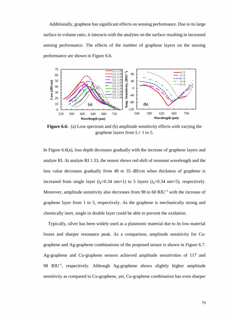
79
Additionally, graphene has significant effects on sensing performance. Due to its large
surface to volume ratio, it interacts with the analytes on the surface resulting in increased
sensing performance. The effects of the number of graphene layers on the sensing
performance are shown in Figure 6.6.
Figure 6.6: (a) Loss spectrum and (b) amplitude sensitivity effects with varying the
graphene layers from L= 1 to 5.
In Figure 6.6(a), loss depth decreases gradually with the increase of graphene layers and
analyte RI. At analyte RI 1.33, the sensor shows red shift of resonant wavelength and the
loss value decreases gradually from 48 to 35 dB/cm when thickness of graphene is
increased from single layer (tg=0.34 nm×1) to 5 layers (tg=0.34 nm×5), respectively.
Moreover, amplitude sensitivity also decreases from 98 to 60 RIU-1 with the increase of
graphene layer from 1 to 5, respectively. As the graphene is mechanically strong and
chemically inert, single or double layer could be able to prevent the oxidation.
Typically, silver has been widely used as a plasmonic material due to its low material
losses and sharper resonance peak. As a comparison, amplitude sensitivity for Cu-
graphene and Ag-graphene combinations of the proposed sensor is shown in Figure 6.7.
Ag-graphene and Cu-graphene sensors achieved amplitude sensitivities of 117 and
98 RIU-1, respectively. Although Ag-graphene shows slightly higher amplitude
sensitivity as compared to Cu-graphene, yet, Cu-graphene combination has even sharper
0
10
20
30
40
50
60
70
520 560 600 640 680 720
Lo
ss (
dB
/cm
)
Wavelength (μm)
L1, 1.33L1, 1.34L2, 1.33L2, 1.34L3, 1.33L3, 1.34L4, 1.33L4, 1.34L5, 1.33L5, 1.34
-120
-80
-40
0
40
80
540 580 620 660 700
Am
p.
Sen
siti
vit
y, (R
IU-1
)
Wavelength (μm)
L=1L=2L=3L=4L=5
(b)(a)

80
resonance peak with more stable plasmonic performance in the long term (Kravets et al.,
2014).
Figure 6.7: Comparison of amplitude sensitivity with graphene coated Cu and Ag
layer, setting na= 1.33, dc = 0.30Λ, d = 0.50Λ, t = tAg= 30 nm and tg= 0.34 nm.
6.5 Summary
In summary, a simple copper-graphene based PCF SPR sensor is proposed. Guiding
properties and sensing performance of the proposed sensor are numerically investigated
by FEM. Proposed sensor shows the maximum wavelength interrogation sensitivity of
2000 nm/RIU and achieve sensor resolution of 5×10⁻⁵ RIU. Furthermore, it shows the
amplitude sensitivity of 140 RIU-1 with the sensor resolution 7.1×10⁻⁵ RIU. The proposed
sensor structure is simpler among the reported PCF SPR sensors which could be realized
using the standard stack-and-draw fabrication method and sputtering, CVD deposition
method.
-130
-80
-30
20
70
440 500 560 620 680
Am
p.
Sen
s. (
RIU
-1)
Wavelength (μm)
Ag-Graphene
Cu-Graphene
81
CHAPTER 7: CONCLUSION AND FUTURE WORKS
7.1 Conclusion
In this study, four different PCF based SPR sensors are developed. Guiding properties
are numerically investigated by commercial COMSOL software. The sensors
performance is observed based on wavelength and amplitude interrogation methods. A
short summary of proposed PCF SPR sensors are given below:
Silver-graphene coated PCF SPR sensor: Considering the selective multiple
metallic channel problem, a single metallic channel (silver with graphene coated) based
PCF SPR sensor is proposed which is comparatively simpler in the fabrication point of
view. Furthermore, only two liquid-filled cores are considered which are placed near to
the metallic channel for easy excitation of free electrons to produce SPW. Silver is used
as a plasmonic material with a thin graphene layer to prevent oxidation. According to the
wavelength interrogation sensitivity, proposed sensor shows the RI sensitivity of 3000
nm/RIU with sensor resolution of 3.33×10⁻⁵ RIU, whereas the average RI sensitivity is
2390 nm/RIU in the sensing range of 1.46 to 1.49. In addition, it shows the amplitude
sensitivity as high as 418 RIU-1 which gives the sensor resolution of 2.4×10⁻⁵ RIU.
However, metal layer coating inside the air-hole surface is quite challenging; as well as
observing the internal sensing is difficult.
Flat fiber based SPR sensor: Flat fiber based SPR sensor is proposed for the first
time in this study. Utilizing the advantage of flat surface, metal layer can be incorporated
easily as well as it turns the simple sensing process. Due to manage the metallic layer
close to the cores which helps to easy excitation of free electrons. Using the proposed
sensor, average wavelength interrogation sensitivity of 9,600 nm/RIU (Refractive Index
Unit) and highest sensitivity of 23,000 nm/RIU are obtained in the sensing range of 1.46-
1.485 and 1.47-1.475, respectively. Moreover, refractive index resolution of 4.35×10⁻⁶ is

82
obtained. Additionally, proposed sensor shown the maximum amplitude interrogation
sensitivity of 820 RIU-1, with the sensor resolution 1.22×10⁻⁵ RIU. The proposed flat fiber
sensor provided the highest wavelength interrogation sensitivity among all the reported
fiber based SPR sensors. The only small challenging part of this sensor is to selectively
infiltrate the liquid.
PCF SPR biosensor with external sensing approach: A simple PCF SPR sensor is
proposed where the metallic layer and sensing layer are placed outside the fiber structure.
Due to outside sensing layer, sensing mechanism will be simple. By using wavelength
and amplitude interrogation methods, the proposed sensor could provide maximum
sensitivities up to 4000 nm/RIU and 320 RIU-1 respectively. The resolutions of the sensor
are 2.5×10⁻⁵ and 3.125×10⁻⁵ RIU for wavelength and amplitude interrogation methods. In
this sensor, the irregular air-holes in the fiber structure can be easily and practically
fabricated by introducing thicker wall capillary.
Copper-graphene based plasmonic biosensor: In this work, for the first time, copper
is utilized as the plasmonic material for PCF SPR sensor. Graphene layer is used to
diminish the oxidation problem. It shows the linear sensing response over the sensing
range. It shows average wavelength interrogation sensitivity of 2000 nm/RIU over the
analyte refractive indices range from 1.33 to 1.37, which leads the sensor resolution of
5×10⁻⁵ RIU.
The proposed sensors in this study, particularly those with external sensing
approaches, breakthrough the PCF SPR sensor technology, that would be very useful for
implementing the fiber SPR sensor practically.
7.2 Future Works
PCF SPR sensing is a promising and competitive sensing technology. However, at the
device development front, PCF SPR sensors are still in an early stage. Most of the work

83
reported in the literature involves proof of concept demonstrations, theoretical and
computational models. The application of established theoretical models to sensor
implementation is limited. Although some experimental devices reported in the literature,
their applications are found in limited research domains. Therefore, the performances of
the modelled sensors are still in question. Potential future work should focus on (i) proof
of concept demonstration to real PCF SPR sensor development, (ii) detection of analytes
from more chemical and biological samples. One possible development direction for the
PCF SPR sensors is portable and rapid lab-on-a-chip assays for point-of-care diagnostics.
Future works that can be carried out for further improving the findings in this study
are as following:
(i) Fabricating the proposed PCFs and combine the plasmonic metal layer outside the
fiber structure to establish the SPR phenomena.
(ii) Observe the sensing performance practically and compare the experimental
results and simulation results.
The PCF SPR sensor shows a promising ability in the detection of chemical and
biological analytes. The performance of the PCF SPR biosensor technology will continue
to evolve with the advances in fabrication technology and the development in metal
nanoparticles. We envision that in future the PCF SPR sensor will become one of the
most popular optical biosensors which will be used in many important sectors such as
medical diagnostics, environmental monitoring, and food safety and security.

84
REFERENCES
Adikan, F. R. M., Sandoghchi, S. R., Yi, C. W., Simpson, R. E., Mahdi, M. A., Webb, A.
S., Holmes, C. (2012). Direct UV written optical waveguides in flexible glass flat
fiber chips. Selected Topics in Quantum Electronics, IEEE Journal of, 18(5),
1534-1539.
Ahmmed, R., Ahmed, R., & Razzak, S. A. (2013). Design of large negative dispersion
and modal analysis for hexagonal, square, FCC and BCC photonic crystal fibers.
Paper presented at the Informatics, Electronics & Vision (ICIEV), 2013
International Conference on.
Akimoto, T., Sasaki, S., Ikebukuro, K., & Karube, I. (1999). Refractive-index and
thickness sensitivity in surface plasmon resonance spectroscopy. Applied optics,
38(19), 4058-4064.
Akowuah, E. K., Gorman, T., Ademgil, H., Haxha, S., Robinson, G. K., & Oliver, J. V.
(2012). Numerical analysis of a photonic crystal fiber for biosensing applications.
Quantum Electronics, IEEE Journal of, 48(11), 1403-1410.
Amouzad Mahdiraji, G. (2015). Low-Crosstalk Semi-Trench-Assisted Multicore Flat
Fiber. Paper presented at the Optical Fiber Communication Conference.
Amouzad Mahdiraji, G., Chow, D. M., Sandoghchi, S., Amirkhan, F., Dermosesian, E.,
Yeo, K. S., . . . Yu Gang, S. (2014). Challenges and solutions in fabrication of
silica-based photonic crystal fibers: An experimental study. Fiber and Integrated
Optics, 33(1-2), 85-104.
Aoni, R. A., Ahmed, R., & Razzak, S. (2013). Design and Simulation of Duel-Concentric-
Core Photonic Crystal Fiber for Dispersion Compensation. Paper presented at the
CIOMP-OSA Summer Session on Optical Engineering, Design and
Manufacturing.
Ashwell, G., & Roberts, M. (1996). Highly selective surface plasmon resonance sensor
for NO 2. Electronics Letters, 32(22), 2089-2091.
Berger, C. E., & Greve, J. (2000). Differential SPR immunosensing. Sensors and
Actuators B: Chemical, 63(1), 103-108.
Biswas, T., Chattopadhyay, R., & Bhadra, S. K. (2014). Plasmonic hollow-core photonic
band gap fiber for efficient sensing of biofluids. Journal of Optics, 16(4), 045001.
Botten, L. C., McPhedran, R. C., de Sterke, C. M., Nicorovici, N. A., Asatryan, A. A.,
Smith, G. H., Kuhlmey, B. T. (2005). From multipole methods to photonic crystal
device modeling. Electromagnetic theory and applications for photonic crystals
(optical engineering), 47-122.
Bunch, J. S., Verbridge, S. S., Alden, J. S., van der Zande, A. M., Parpia, J. M., Craighead,
H. G., & McEuen, P. L. (2008). Impermeable atomic membranes from graphene
sheets. Nano letters, 8(8), 2458-2462.

85
Cahill, C. P., Johnston, K. S., & Yee, S. S. (1997). A surface plasmon resonance sensor
probe based on retro-reflection. Sensors and Actuators B: Chemical, 45(2), 161-
166.
Cheng, D. K. (1989). Field and wave electromagnetics (Vol. 2): Addison-wesley New
York.
Cheng, Y.-C., Su, W.-K., & Liou, J.-H. (2000). Application of a liquid sensor based on
surface plasma wave excitation to distinguish methyl alcohol from ethyl alcohol.
Optical Engineering, 39(1), 311-314.
Choi, S. H., Kim, Y. L., & Byun, K. M. (2011). Graphene-on-silver substrates for
sensitive surface plasmon resonance imaging biosensors. Optics express, 19(2),
458-466.
Cinteza, L. O., Ohulchanskyy, T. Y., Sahoo, Y., Bergey, E. J., Pandey, R. K., & Prasad,
P. N. (2006). Diacyllipid micelle-based nanocarrier for magnetically guided
delivery of drugs in photodynamic therapy. Molecular pharmaceutics, 3(4), 415-
423.
Cooper, M. A. (2002). Optical biosensors in drug discovery. Nature Reviews Drug
Discovery, 1(7), 515-528.
Daghestani, H. N., & Day, B. W. (2010). Theory and applications of surface plasmon
resonance, resonant mirror, resonant waveguide grating, and dual polarization
interferometry biosensors. Sensors, 10(11), 9630-9646.
Dash, J. N., & Jha, R. (2014a). Graphene-based birefringent photonic crystal fiber sensor
using surface plasmon resonance. Photonics Technology Letters, IEEE, 26(11),
1092-1095.
Dash, J. N., & Jha, R. (2014b). SPR Biosensor Based on Polymer PCF Coated With
Conducting Metal Oxide. IEEE Photonics Technology Letters, 26(6), 595-598.
doi:10.1109/lpt.2014.2301153
Dash, J. N., & Jha, R. (2015a). On the Performance of Graphene-Based D-Shaped
Photonic Crystal Fibre Biosensor Using Surface Plasmon Resonance. Plasmonics,
1-9.
Dash, J. N., & Jha, R. (2015b). On the Performance of Graphene-Based D-Shaped
Photonic Crystal Fibre Biosensor Using Surface Plasmon Resonance. Plasmonics,
10, 1123–1131.
DeVore, J. R. (1951). Refractive indices of rutile and sphalerite. JOSA, 41(6), 416-417.
Dular, P., Meunier, G., Piriou, F., Ould Agha, Y., Zolla, F., Nicolet, A., & Guenneau, S.
(2008). On the use of PML for the computation of leaky modes: an application to
microstructured optical fibres. COMPEL-The international journal for
computation and mathematics in electrical and electronic engineering, 27(1), 95-
109.

86
Egorova, O., Semjonov, S., Senatorov, A., Salganskii, M., Koklyushkin, A., Nazarov, V.,
Dianov, E. (2014). Multicore fiber with rectangular cross-section. Optics letters,
39(7), 2168-2170.
Emmerich, G. Surface Plasmon Resonance: Technology Overview and Practical
Applications.
Fang, Y. (2006). Label-free cell-based assays with optical biosensors in drug discovery.
Assay and drug development technologies, 4(5), 583-595.
Fu, X., Lu, Y., Huang, X., & Yao, J. (2011). Surface plasmon resonance sensor based on
photonic crystal fiber filled with silver nanowires. Opt. Appl, 41(4), 941-951.
Gallagher, D. F., & Felici, T. P. (2003). Eigenmode expansion methods for simulation of
optical propagation in photonics: pros and cons. Paper presented at the Integrated
Optoelectronics Devices.
Gao, D., Guan, C., Wen, Y., Zhong, X., & Yuan, L. (2014). Multi-hole fiber based surface
plasmon resonance sensor operated at near-infrared wavelengths. Optics
Communications, 313, 94-98.
Gauvreau, B., Hassani, A., Fassi Fehri, M., Kabashin, A., & Skorobogatiy, M. A. (2007).
Photonic bandgap fiber-based surface plasmon resonance sensors. Optics express,
15(18), 11413-11426.
Guo, J., Liu, Y.-g., Wang, Z., Han, T., Huang, W., & Luo, M. (2014). Tunable fiber
polarizing filter based on a single-hole-infiltrated polarization maintaining
photonic crystal fiber. Optics express, 22(7), 7607-7616.
Gupta, B., & Verma, R. (2009). Surface plasmon resonance-based fiber optic sensors:
principle, probe designs, and some applications. Journal of Sensors, 2009.
Hassani, A., Gauvreau, B., Fehri, M. F., Kabashin, A., & Skorobogatiy, M. (2008).
Photonic crystal fiber and waveguide-based surface plasmon resonance sensors
for application in the visible and near-IR. Electromagnetics, 28(3), 198-213.
Hassani, A., & Skorobogatiy, M. (2006). Design of the microstructured optical fiber-
based surface plasmon resonance sensors with enhanced microfluidics. Optics
express, 14(24), 11616-11621.
Hassani, A., & Skorobogatiy, M. (2009). Photonic crystal fiber-based plasmonic sensors
for the detection of biolayer thickness. JOSA B, 26(8), 1550-1557.
Holmes, C., Adikan, F. R., Webb, A. S., Gates, J. C., Gawith, C. B., Sahu, J. K., Payne,
D. N. (2008). Evanescent field sensing in novel flat fiber. Paper presented at the
Conference on Lasers and Electro-Optics.
Homola, J. (2003). Present and future of surface plasmon resonance biosensors.
Analytical and bioanalytical chemistry, 377(3), 528-539.
Homola, J. (2006). Surface plasmon resonance based sensors (Vol. 4): Springer Science
& Business Media.

87
Homola, J. (2008). Surface plasmon resonance sensors for detection of chemical and
biological species. Chemical reviews, 108(2), 462-493.
Homola, J., Yee, S. S., & Gauglitz, G. (1999). Surface plasmon resonance sensors:
review. Sensors and Actuators B: Chemical, 54(1), 3-15.
Ismach, A., Druzgalski, C., Penwell, S., Schwartzberg, A., Zheng, M., Javey, A., Zhang,
Y. (2010). Direct chemical vapor deposition of graphene on dielectric surfaces.
Nano letters, 10(5), 1542-1548.
Jie, Z., Dakai, L., & Zhenwu, Z. (2007). Reflective optical fiber surface plasma wave
resonance sensor. Acta Optica Sinica, 27(3), 404.
Johnson, S., & Joannopoulos, J. (2001). Block-iterative frequency-domain methods for
Maxwell's equations in a planewave basis. Optics express, 8(3), 173-190.
Johnston, K. S., Karlsen, S. R., Jung, C. C., & Yee, S. S. (1995). New analytical technique
for characterization of thin films using surface plasmon resonance. Materials
chemistry and physics, 42(4), 242-246.
Jorgenson, R., & Yee, S. (1993). A fiber-optic chemical sensor based on surface plasmon
resonance. Sensors and Actuators B: Chemical, 12(3), 213-220.
Kajenski, P. J. (1997). Tunable optical filter using long-range surface plasmons. Optical
Engineering, 36(5), 1537-1541.
Kanso, M., Cuenot, S., & Louarn, G. (2007). Roughness effect on the SPR measurements
for an optical fibre configuration: experimental and numerical approaches.
Journal of Optics A: Pure and Applied Optics, 9(7), 586.
Khan, I. (2012). Optical fiber based microwaves sensor using surface plasmon
resonance. Paper presented at the Informatics, Electronics & Vision (ICIEV),
2012 International Conference on.
Kim, J. A., Hwang, T., Dugasani, S. R., Amin, R., Kulkarni, A., Park, S. H., & Kim, T.
(2013). Graphene based fiber optic surface plasmon resonance for bio-chemical
sensor applications. Sensors and Actuators B: Chemical, 187, 426-433.
Kiraly, B., Iski, E. V., Mannix, A. J., Fisher, B. L., Hersam, M. C., & Guisinger, N. P.
(2013). Solid-source growth and atomic-scale characterization of graphene on Ag
(111). Nature communications, 4.
Knoll, W. (1998). Interfaces and thin films as seen by bound electromagnetic waves.
Annual Review of Physical Chemistry, 49(1), 569-638.
Koshiba, M. (1992). Optical waveguide theory by the finite element method.
Koshiba, M., & Saitoh, K. (2001). Numerical verification of degeneracy in hexagonal
photonic crystal fibers. Ieee Photonics Technology Letters, 13(12), 1313-1315.

88
Kotynski, R., Antkowiak, M., Berghmans, F., Thienpont, H., & Panajotov, K. (2005).
Photonic crystal fibers with material anisotropy. Optical and quantum electronics,
37(1-3), 253-264.
Kravets, V., Jalil, R., Kim, Y.-J., Ansell, D., Aznakayeva, D., Thackray, B., . . . Radko,
I. (2014). Graphene-protected copper and silver plasmonics. Scientific reports, 4.
KretschmannE, R. (1968). Radiativedecayofnon radiative surface plasmons excited by
light. Z Naturforsch, 23, 2135–2136
Kuhlmey, B. T., Eggleton, B. J., & Wu, D. K. (2009). Fluid-filled solid-core photonic
bandgap fibers. Journal of Lightwave Technology, 27(11), 1617-1630.
Liedberg, B., Nylander, C., & Lunström, I. (1983). Surface plasmon resonance for gas
detection and biosensing. Sensors and actuators, 4, 299-304.
Lu, Y., Hao, C.-J., Wu, B.-Q., Huang, X.-H., Wen, W.-Q., Fu, X.-Y., & Yao, J.-Q. (2012).
Grapefruit fiber filled with silver nanowires surface plasmon resonance sensor in
aqueous environments. Sensors, 12(9), 12016-12025.
Lu, Y., Hao, C.-J., Wu, B.-Q., Musideke, M., Duan, L.-C., Wen, W.-Q., & Yao, J.-Q.
(2013). Surface plasmon resonance sensor based on polymer photonic crystal
fibers with metal nanolayers. Sensors, 13(1), 956-965.
Lu, Y., Yang, X., Wang, M., & Yao, J. (2015). Surface plasmon resonance sensor based
on hollow-core PCFs filled with silver nanowires. Electronics Letters, 51(21),
1675-1677.
Luan, N., Wang, R., Lv, W., & Yao, J. (2015). Surface plasmon resonance sensor based
on D-shaped microstructured optical fiber with hollow core. Optics express,
23(7), 8576-8582.
Maharana, P. K., & Jha, R. (2012). Chalcogenide prism and graphene multilayer based
surface plasmon resonance affinity biosensor for high performance. Sensors and
Actuators B: Chemical, 169, 161-166.
Mahdiraji, G. A., Amirkhan, F., Chow, D. M., Kakaie, Z., Yong, P. S., Dambul, K. D., &
Adikan, F. R. M. (2014). Multicore Flat Fiber: A New Fabrication Technique.
Photonics Technology Letters, IEEE, 26(19), 1972-1974.
Malinský, P., Slepička, P., Hnatowicz, V., & Švorčík, V. (2012). Early stages of growth
of gold layers sputter deposited on glass and silicon substrates. Nanoscale
research letters, 7(1), 1-7.
Mishra, A. K., Mishra, S. K., & Gupta, B. D. (2015). SPR based fiber optic sensor for
refractive index sensing with enhanced detection accuracy and figure of merit in
visible region. Optics Communications, 344, 86-91.
Myszka, D. G. (1999). Improving biosensor analysis. Journal of Molecular Recognition,
12(5), 279-284.

89
Naik, G. V., Shalaev, V. M., & Boltasseva, A. (2013). Alternative plasmonic materials:
beyond gold and silver. Advanced Materials, 25(24), 3264-3294.
Niggemann, M., Katerkamp, A., Pellmann, M., Bolsmann, P., Reinbold, J., & Cammann,
K. (1996). Remote sensing of tetrachloroethene with a micro-fibre optical gas
sensor based on surface plasmon resonance spectroscopy. Sensors and Actuators
B: Chemical, 34(1), 328-333.
Ortega-Mendoza, J. G., Padilla-Vivanco, A., Toxqui-Quitl, C., Zaca-Morán, P., Villegas-
Hernández, D., & Chávez, F. (2014). Optical Fiber Sensor Based on Localized
Surface Plasmon Resonance Using Silver Nanoparticles Photodeposited on the
Optical Fiber End. Sensors, 14(10), 18701-18710.
Otto, A. (1968). Excitation of nonradiative surface plasma waves in silver by the method
of frustrated total reflection. Zeitschrift für Physik, 216(4), 398-410.
Otupiri, R., Akowuah, E., & Haxha, S. (2015). Multi-channel SPR biosensor based on
PCF for multi-analyte sensing applications. Optics express, 23(12), 15716-15727.
Otupiri, R., Akowuah, E., Haxha, S., Ademgil, H., AbdelMalek, F., & Aggoun, A. (2014).
A novel birefrigent photonic crystal fiber surface plasmon resonance biosensor.
Photonics Journal, IEEE, 6(4), 1-11.
Palik, E. D. (1998). Handbook of optical constants of solids (Vol. 3): Academic press.
Pearce, G., Hedley, T., & Bird, D. (2005). Adaptive curvilinear coordinates in a plane-
wave solution of Maxwell’s equations in photonic crystals. Physical Review B,
71(19), 195108.
Poletti, F. (2007). Direct and inverse design of microstructured optical fibres. University
of Southampton.
Qin, W., Li, S., Yao, Y., Xin, X., & Xue, J. (2014). Analyte-filled core self-calibration
microstructured optical fiber based plasmonic sensor for detecting high refractive
index aqueous analyte. Optics and Lasers in Engineering, 58, 1-8.
Rakic, A. D., Djurišic, A. B., Elazar, J. M., & Majewski, M. L. (1998). Optical properties
of metallic films for vertical-cavity optoelectronic devices. Applied optics, 37(22),
5271-5283.
Rhodes, C., Cerruti, M., Efremenko, A., Losego, M., Aspnes, D., Maria, J.-P., & Franzen,
S. (2008). Dependence of plasmon polaritons on the thickness of indium tin oxide
thin films. Journal of Applied Physics, 103(9), 093108.
Ritchie, R. (1957). Plasma losses by fast electrons in thin films. Physical Review, 106(5),
874.
Salihoglu, O., Balci, S., & Kocabas, C. (2012). Plasmon-polaritons on graphene-metal
surface and their use in biosensors. Applied Physics Letters, 100(21), 213110.

90
Sazio, P. J., Amezcua-Correa, A., Finlayson, C. E., Hayes, J. R., Scheidemantel, T. J.,
Baril, N. F., Margine, E. R. (2006). Microstructured optical fibers as high-pressure
microfluidic reactors. science, 311(5767), 1583-1586.
Schildkraut, J. S. (1988). Long-range surface plasmon electrooptic modulator. Applied
optics, 27(21), 4587-4590.
Schriver, M., Regan, W., Gannett, W. J., Zaniewski, A. M., Crommie, M. F., & Zettl, A.
(2013). Graphene as a long-term metal oxidation barrier: worse than nothing. ACS
nano, 7(7), 5763-5768.
Sharma, A. K., Jha, R., & Gupta, B. (2007). Fiber-optic sensors based on surface plasmon
resonance: a comprehensive review. Sensors Journal, IEEE, 7(8), 1118-1129.
Shi, F., Peng, L., Zhou, G., Cang, X., Hou, Z., & Xia, C. (2015). An Elliptical Core D-
Shaped Photonic Crystal Fiber-Based Plasmonic Sensor at Upper Detection
Limit. Plasmonics, 1-6.
Shuai, B., Xia, L., & Liu, D. (2012). Coexistence of positive and negative refractive index
sensitivity in the liquid-core photonic crystal fiber based plasmonic sensor. Optics
express, 20(23), 25858-25866.
Shuai, B., Xia, L., Zhang, Y., & Liu, D. (2012). A multi-core holey fiber based plasmonic
sensor with large detection range and high linearity. Optics express, 20(6), 5974-
5986.
Sincerbox, G. T., & Gordon, J. C. (1981). Small fast large-aperture light modulator using
attenuated total reflection. Applied optics, 20(8), 1491-1496.
Slavık, R., Homola, J., & Čtyroký, J. (1999). Single-mode optical fiber surface plasmon
resonance sensor. Sensors and Actuators B: Chemical, 54(1), 74-79.
Snyder, A. W., & Love, J. (2012). Optical waveguide theory: Springer Science &
Business Media.
Stemmler, I., Brecht, A., & Gauglitz, G. (1999). Compact surface plasmon resonance-
transducers with spectral readout for biosensing applications. Sensors and
Actuators B: Chemical, 54(1), 98-105.
Su, Y.-T., Chen, S.-J., & Yeh, T.-L. (2005). A common-path phase-shift interferometry
surface plasmon imaging system. Paper presented at the Biomedical Optics 2005.
Takeyasu, N., Tanaka, T., & Kawata, S. (2005). Metal deposition deep into
microstructure by electroless plating. Japanese journal of applied physics,
44(8L), L1134.
Tan, Z., Li, X., Chen, Y., & Fan, P. (2014). Improving the sensitivity of fiber surface
plasmon resonance sensor by filling liquid in a hollow core photonic crystal fiber.
Plasmonics, 9(1), 167-173.

91
Tian, M., Lu, P., Chen, L., Lv, C., & Liu, D. (2012). All-solid D-shaped photonic fiber
sensor based on surface plasmon resonance. Optics Communications, 285(6),
1550-1554.
Vial, A., Grimault, A.-S., Macías, D., Barchiesi, D., & de La Chapelle, M. L. (2005).
Improved analytical fit of gold dispersion: Application to the modeling of
extinction spectra with a finite-difference time-domain method. Physical Review
B, 71(8), 085416.
Viale, P., Février, S., Gérôme, F., & Vilard, H. (2005). Confinement loss computations in
photonic crystal fibres using a novel perfectly matched layer design. Paper
presented at the Femlab Conference.
Vieweg, M., Gissibl, T., Pricking, S., Kuhlmey, B., Wu, D., Eggleton, B., & Giessen, H.
(2010). Ultrafast nonlinear optofluidics in selectively liquid-filled photonic
crystal fibers. Optics express, 18(24), 25232-25240.
Wang, Y. (1995). Voltage induced color selective absorption with surface plasmons.
Applied Physics Letters, 67(19), 2759-2761.
West, P. R., Ishii, S., Naik, G. V., Emani, N. K., Shalaev, V. M., & Boltasseva, A. (2010).
Searching for better plasmonic materials. Laser & Photonics Reviews, 4(6), 795-
808.
White, T., Kuhlmey, B., McPhedran, R., Maystre, D., Renversez, G., De Sterke, C. M.,
& Botten, L. (2002). Multipole method for microstructured optical fibers. I.
Formulation. JOSA B, 19(10), 2322-2330.
Wong, W. R., Krupin, O., Sekaran, S. D., Mahamd Adikan, F. R., & Berini, P. (2014).
Serological diagnosis of dengue infection in blood plasma using long-range
surface plasmon waveguides. Analytical chemistry, 86(3), 1735-1743.
Wu, C., Tse, M.-L. V., Liu, Z., Guan, B.-O., Lu, C., & Tam, H.-Y. (2013). In-line
microfluidic refractometer based on C-shaped fiber assisted photonic crystal fiber
Sagnac interferometer. Optics letters, 38(17), 3283-3286.
Wu, L., Chu, H., Koh, W., & Li, E. (2010). Highly sensitive graphene biosensors based
on surface plasmon resonance. Optics express, 18(14), 14395-14400.
Wu, Y., Yao, B., Zhang, A., Rao, Y., Wang, Z., Cheng, Y., . . . Chiang, K. (2014).
Graphene-coated microfiber Bragg grating for high-sensitivity gas sensing.
Optics letters, 39(5), 1235-1237.
Yeh, P., Yariv, A., & Hong, C.-S. (1977). Electromagnetic propagation in periodic
stratified media. I. General theory. JOSA, 67(4), 423-438.
Yu, X., Zhang, Y., Pan, S., Shum, P., Yan, M., Leviatan, Y., & Li, C. (2010). A selectively
coated photonic crystal fiber based surface plasmon resonance sensor. Journal of
Optics, 12(1), 015005.
Yuan, G., Gao, L., Chen, Y., Liu, X., Wang, J., & Wang, Z. (2014). Improvement of
optical sensing performances of a double-slot-waveguide-based ring resonator

92
sensor on silicon-on-insulator platform. Optik-International Journal for Light and
Electron Optics, 125(2), 850-854.
Zhang, P.-p., Yao, J.-q., Cui, H.-x., & Lu, Y. (2013). A surface plasmon resonance sensor
based on a multi-core photonic crystal fiber. Optoelectronics Letters, 9, 342-345.
Zhao, Y., Deng, Z.-q., & Li, J. (2014). Photonic crystal fiber based surface plasmon
resonance chemical sensors. Sensors and Actuators B: Chemical, 202, 557-567.
Zynio, S. A., Samoylov, A. V., Surovtseva, E. R., Mirsky, V. M., & Shirshov, Y. M.
(2002). Bimetallic layers increase sensitivity of affinity sensors based on surface
plasmon resonance. Sensors, 2(2), 62-70.

93
LIST OF PUBLICATIONS
Journal Papers:
Ahmmed A. Rifat, G. Amouzad Mahdiraji, Rajib Ahmed, Desmond M. Chow ,
Y. M. Sua, Y. G. Shee, M. R. A. Adikan, “Copper-Graphene Based Photonic
Crystal Fiber Plasmonic Biosensor”, IEEE Photonics Journal, Issue: 1, vol: 8,
2016. (ISI-cited-Q1)
A. A. Rifat, G. Amouzad Mahdiraji, Y. M. Sua, Y. G. Shee, Rajib Ahmed,
Desmond M. Chow, F. R. Mahamd Adikan, “Surface Plasmon Resonance
Photonic Crystal Fiber Biosensor: A Practical Sensing Approach”, IEEE Photonics
Technology Letters, Issue: 15, Vol. 27, pp: 1628-1631, 2015. (ISI-cited-Q1)
Ahmmed A. Rifat, G. Amouzad Mahdiraji, Desmond M. Chow, Y. G. Shee, Rajib
Ahmed, Desmond M. Chow, F. R. M. Adikan, “Photonic Crystal Fiber based
Surface Plasmon Resonance Sensor with Selective Analyte Channels and
Graphene-Silver Deposited Core”, Sensors, Vol. 15, pp. 11499-11510, 2015. (ISI-
cited-Q1)
Ahmmed A. Rifat, G. Amouzad Mahdiraji, Y. M. Sua, Rajib Ahmed, Y. G. Shee,
M. R. A. Adikan, “Highly Sensitive Multicore Flat Fiber Surface Plasmon
Resonance Refractive Index Sensor”, Optics Express (Accepted, in press). (ISI-
cited-Q1)
Proceeding/Conference Papers:
A. A. Rifat, G. Amouzad Mahdiraji, Y. G. Shee, Md. Jubayer Shawan, F. R.
Mahamd Adikan, “A Novel Photonic Crystal Fiber Biosensor Based on Surface
Plasmon Resonance”, 4th Photonics Global Conference (ICMAT-2015), 28 June -
03 July, 2015, Singapore.
A. A. Rifat, G. A. Mahdiraji, Y.G. Shee, F.R.M. Adikan, “Flat Fiber Based Surface
Plasmon Resonance Sensor”, Siegman International School on Lasers: 2015,
Organized by Max Planck Institute, Germany, 02-07 August, 2015 (Awarded
partial travel grant from Optical Society of America (OSA) to attend this
conference).
A. A. Rifat, Ghafour Amouzad Mahdiraji, Y.G. Shee, F.R.M. Adikan, “Design of
Dispersion Manage, Low Confinement Loss and High Nonlinearity Photonic
Crystal Fiber for Communication Applications”, 6th AUN/SEED-Net Regional
Conference on Electrical Engineering, 4-5th March, 2014, Malaysia.