modeling, growth and characterization of ingaas …schenk/theses/thesis_saurabh1.pdf · parameters...
TRANSCRIPT

Institut fur Integrierte Systeme
Integrated Systems Laboratory
Department of Information Technology andElectrical Engineering
Fall Term 2013
Modeling, Growth andCharacterization of InGaAs
Nanowires
Master Project
Saurabh [email protected]
December 2013
Supervisors: Dr. Heike Riel, [email protected]. Mattias Borg, [email protected]
Professor: Prof. Andreas Schenk, [email protected]

Acknowledgments
First of all, I would like to thank IBM Research, Zurich for offering me a fabricationrelated project. The project was quite interesting. I learned a lot, not just about thetechnology and processes, but also about how to perform experiments in a well organizedway. I wish to thank Mattias and Kirsten for training me to perform the whole templatefabrication processes given that I had no prior experience in the fabrication whatsoever.Then, I wish to thank Mattias again for performing x-ray diffraction spectroscopy on theInGaAs nanowire samples. I wish to thank Giorgio for performing Raman spectroscopyon my samples. I would like to thank Frederik for providing me the pseudopotentialparameters and a workbench for the band structure calculations. Finally, I would liketo thank Prof. Schenk and Dr. Riel for supervising the project and providing valuableinputs time-to-time.
ii

Abstract
After around four decades of development at an exponential rate, the Silicon fabricationtechnology is now highly advanced and on the edge of maturity. The shortcomings of Sias a material have now surfaced and it is no longer possible to improve the performanceof the devices using Si technology. Among the alternative materials, III-V compoundsemiconductors provide a viable alternative to Si. Integration of the III-V materials on Sican utilize both the advantages of III-V and well-developed Si technology. Additionally,future electronic devices will probably utilize the nanowire geometry. Therefore, theintegration of III-V materials on Si in the form of nanowires has high potential in deviceapplications.
The goal of the project is to grow vertical InGaAs nanowires on Si by OrganometallicVapour Phase Epitaxy(MOVPE). In this project, well-like templates with oxide walls andthe base made of Si surface have been fabricated on Si(111) substrates. The InGaAsnanowires have been grown on the Si surface inside the template by using selectivearea epitaxy. In the MOVPE growth of InGaAs nanowires, the ratio of In to Ga flowrate was varied from sample to sample. The InGaAs nanowires were characterized byRaman and x-ray diffraction spectroscopy to determine the mole fraction of Ga in thenanowires. The mole fraction of Ga incorporated in InGaAs nanowires shows nonlinearrelation with the mole fraction of Ga in the vapour phase. An empirical relationshipbetween the Ga mole fractions in InGaAs nanowires and in vapour phase is obtainedusing the characterization results. This calibration will be useful in the growth of InGaAsnanowires with predetermined Ga mole fraction by setting proper ratios of In and Gaflow rates.
In addition to the fabrication, the pseudopotential calculations of InxGa1−xAs/GaAs1−ySby
alloy system have been carried out to extract the band structure parameters of the sys-tem. Based on these parameters, a rough estimate on the most suitable compositionsof alloys for InGaAs/GaAsSb heterojunction TFETs has been obtained. It is expectedthat the composition range having lattice matched alloys that show slightly staggeredband edge alignment will be most suitable for heterojunction TFET applications.
iii

Declaration of Authorship
I hereby declare that the presented master thesis is self composed and written only bymeans and sources as specified in the text and acknowledgements. The final thesis orsimilar versions of it have so far not been submitted to any other examination board.
Saurabh Sant,Zurich, December 2013
iv

Contents
1 Introduction 1
2 Modeling the effect of mismatch strain in InGaAs/GaAsSb alloy sys-tem 32.1 Strain calculations in lattice mismatched alloy systems . . . . . . . . . . . 32.2 Empirical pseudopotential method . . . . . . . . . . . . . . . . . . . . . . 4
2.2.1 Pseudopotential method for compound semiconductors . . . . . . . 52.2.2 Virtual Crystal Approximation . . . . . . . . . . . . . . . . . . . . 52.2.3 Modeling the effect of strain . . . . . . . . . . . . . . . . . . . . . . 62.2.4 Parameters used for pseudopotential calculations . . . . . . . . . . 6
2.3 Pseudopotential calculations of InGaAs/GaAsSb alloy system . . . . . . . 82.3.1 Extraction of tunnel gap and effective mass values . . . . . . . . . 92.3.2 The tunnel probability and its direction dependence . . . . . . . . 102.3.3 ION/IOFF ratio in T-FETs and direction dependence . . . . . . . . 122.3.4 Limitations of the above analysis . . . . . . . . . . . . . . . . . . . 15
2.4 Conclusions . . . . . . . . . . . . . . . . . . . . . . . . . . . . . . . . . . . 16
3 Overview of Template Fabrication 173.1 Template fabrication process flow . . . . . . . . . . . . . . . . . . . . . . . 17
4 Brief Description of Fabrication Processes 204.1 Dry Etching Techniques . . . . . . . . . . . . . . . . . . . . . . . . . . . . 20
4.1.1 Principle of reactive ion etching . . . . . . . . . . . . . . . . . . . . 204.1.2 Reactive Ion Etching of oxide . . . . . . . . . . . . . . . . . . . . . 224.1.3 Inductively coupled plasma - reactive ion etching . . . . . . . . . . 22
4.2 Wet Etching Techniques . . . . . . . . . . . . . . . . . . . . . . . . . . . . 234.2.1 HF etching of oxide . . . . . . . . . . . . . . . . . . . . . . . . . . 234.2.2 Hydroxide etch of Silicon . . . . . . . . . . . . . . . . . . . . . . . 24
4.3 Plasma Enhanced Chemical Vapour Deposition . . . . . . . . . . . . . . . 254.3.1 oxide deposition using Silane . . . . . . . . . . . . . . . . . . . . . 26
v

Contents
4.3.2 oxide deposition using TEOS . . . . . . . . . . . . . . . . . . . . . 274.3.3 Rapid Thermal Processing . . . . . . . . . . . . . . . . . . . . . . . 27
5 Heteroepitaxial growth of InGaAs - Theory 285.1 Epitaxial growth of InGaAs . . . . . . . . . . . . . . . . . . . . . . . . . . 28
5.1.1 Methods of epitaxial growth . . . . . . . . . . . . . . . . . . . . . . 285.1.2 Growth Mechanism of InGaAs in MOVPE . . . . . . . . . . . . . . 30
5.2 Heteroepitaxy of InGaAs on Si . . . . . . . . . . . . . . . . . . . . . . . . 325.2.1 Nucleation and growth of InGaAs over Si . . . . . . . . . . . . . . 325.2.2 Effect of Si surface . . . . . . . . . . . . . . . . . . . . . . . . . . . 335.2.3 Effect of strain . . . . . . . . . . . . . . . . . . . . . . . . . . . . . 33
5.3 Templated growth of InGaAs nanowires . . . . . . . . . . . . . . . . . . . 34
6 Templated Growth of InGaAs Nanowires 376.1 Fabrication of Silicon Nanopillars . . . . . . . . . . . . . . . . . . . . . . . 37
6.1.1 Nanoparticle Mask Preparation . . . . . . . . . . . . . . . . . . . . 376.1.2 RIE - Transfer of nanoparticle mask to oxide . . . . . . . . . . . . 386.1.3 ICP RIE - Fabrication of Si nanopillars . . . . . . . . . . . . . . . 40
6.2 Oxide Template Fabrication . . . . . . . . . . . . . . . . . . . . . . . . . . 416.2.1 Deposition of Si Oxide for template walls . . . . . . . . . . . . . . 416.2.2 Opening the cap on Si nanopillars . . . . . . . . . . . . . . . . . . 426.2.3 Template fabrication . . . . . . . . . . . . . . . . . . . . . . . . . . 43
6.3 Epitaxial Growth of InGaAs Nanowires . . . . . . . . . . . . . . . . . . . 446.4 Summary . . . . . . . . . . . . . . . . . . . . . . . . . . . . . . . . . . . . 50
7 Characterization of InGaAs Nanowires 517.1 X-Ray diffraction study of the InGaAs nano-pillars . . . . . . . . . . . . . 51
7.1.1 Theoretical Background . . . . . . . . . . . . . . . . . . . . . . . . 517.1.2 Results . . . . . . . . . . . . . . . . . . . . . . . . . . . . . . . . . 537.1.3 Discussions . . . . . . . . . . . . . . . . . . . . . . . . . . . . . . . 53
8 Conclusions 578.1 Optimization of template fabrication process . . . . . . . . . . . . . . . . 578.2 Growth of InGaAs inside the templates . . . . . . . . . . . . . . . . . . . 58
vi

List of Figures
2.1 Fitting of the calculated electron effective mass with experimental datathroughout the composition range. . . . . . . . . . . . . . . . . . . . . . . 8
2.2 The tunnel gap at InGaAs/GaAsSb heterojunction . . . . . . . . . . . . . 92.3 The electron effective mass along important crystallographic directions . . 102.4 The light hole effective mass along important crystallographic directions . 112.5 The tunnel probability and its direction dependence . . . . . . . . . . . . 112.6 Factors influencing ON-OFF ratio in a TFET and the Figure of Merit . . 132.7 Figure of Merit of p-/n- channel TFETs and its directional dependence . 142.8 Effect of Fermi level on Tunnel Gap . . . . . . . . . . . . . . . . . . . . . 15
3.1 Overview of the template fabrication process . . . . . . . . . . . . . . . . 19
4.1 Anisotropy achieved in reactive ion etching . . . . . . . . . . . . . . . . . 214.2 SEM view of the cross-section of oxide layer . . . . . . . . . . . . . . . . . 26
5.1 Effect of monoatomic and diatomic steps in Si substrate on InGaAs growth 345.2 Schematic of InGaAs nanowire growth by selective epitaxy . . . . . . . . . 355.3 Schematic of template based growth of InGaAs nanowires . . . . . . . . . 36
6.1 Optimization of RIE process by varying O2/CHF3 gas flow ratio . . . . . 396.2 Determination of optimal ratio of HBr/O2 flow rates . . . . . . . . . . . . 396.3 The substrate and Si nanopillars after cap opening . . . . . . . . . . . . . 436.4 Templates obtained by Si nanopillar etch . . . . . . . . . . . . . . . . . . 446.5 Templates filled with InGaAs . . . . . . . . . . . . . . . . . . . . . . . . . 476.6 InGaAs nanopillars grown at different vapour phase Ga mole fractions . . 486.7 SEM images of some peculiar nanopillars . . . . . . . . . . . . . . . . . . 49
7.1 Results of XRD measurements on InGaAs nanowires . . . . . . . . . . . . 547.2 Distribution coefficient of Ga in the templated growth of InGaAs . . . . . 56
vii

List of Tables
2.1 Comparison of band energies and effective masses with experimental data 72.2 Comparison of the deformation potentials with experimental data . . . . 7
6.1 Template dimensions . . . . . . . . . . . . . . . . . . . . . . . . . . . . . . 456.2 Conditions of MOVPE growth for InGaAs nanowires on different samples 46
7.1 Analysis of XRD measurements . . . . . . . . . . . . . . . . . . . . . . . . 55
viii

Chapter 1Introduction
The phenomenological growth of semiconductor industry in past few decades was a resultof technological advancements, in particular in Si fabrication technology. This technologyis now way more advanced and well matured. But, improved technology cannot overcomethe shortcomings due to inherent properties of Si. For example, indirect nature of theband gap of Si prevents its use in photonic devices. Besides, the low electron andhole mobility necessitates large gate overdrive which restricts voltage and power scalingcapabilities of Si MOSFETs. This lead semiconductor technologists to explore alternatesemiconducting materials which will not suffer from above drawbacks. To counter lowhole mobility in Si MOSFETs, the technologists are trying Ge as a replacement of Si.However, Ge also suffers from the shortcomings of an indirect band gap. The III-Vcompound semiconductors are considered as promising materials for electronic devicesas well as photonics due to high carrier mobilities and direct band gap. Therefore, theirviability to replace Si in semiconductor technology is being explored.
Perhaps the major drawback of switching to III-V semiconductors for nano-electronicsis that, the fabrication technology for these materials is not matured yet. A probablesolution would be to investigate the technologies which can integrate III-V devices onSi. This approach would combine the benefits of matured Si technology and the advan-tages of III-V materials. Attempts are being made to integrate III-V photonic devicessuch as lasers, photodetectors, microwave electronic devices like high electron mobilitytransistors(HEMTS) and logic devices such as MOSFETs on Si[1].
In addition to the limitations of Si as a material, a MOSFET as a logic device suffersfrom a limitation that the threshold voltage in the MOSFET cannot be scaled downfurther without increasing the off-state leakage currents. This limitation stems from themechanism of thermionic emission which is responsible to turn-off the device. Since itis inherent in the device working principle, it cannot be eliminated by selecting different
1

1 Introduction
materials or device geometries. To overcome this limitation, a logic device named Tun-nel Field Effect Transistor(TFET) which is based on tunneling of the carriers is beingexplored as an alternative for MOSFETs[2].
Device geometry plays an important role not just in improving the performance of thedevices, but also in determining the simplest geometries that deliver high performanceand also are technologically preferred. The nanowire-based gate-all-around approachhas shown to perform well for FET-like devices. It offers higher electrostatic integrityand scaling potential. It is, therefore, useful to develop future technologies aiming atthe nanowire-based devices[3]. The template based epitaxy, in which III-V materials aregrown in a well-like oxide template having Si surface at the base, is more suitable forthe growth of vertical InGaAs nanowires with cylindrical shape.
In this project, the nanowires made of InGaAs alloy with different Ga mole fraction arefabricated by template based epitaxy. Metal Organic Vapour Phase Epitaxy(MOVPE)technique is used for the growth of the alloy. In this technique, the organometallicprecursors of In and Ga are passed over the substrate along with the precursor of As.Variation in Ga mole fraction in growing InGaAs can be achieved by changing relativeflow rates of the precursors of In and Ga. Usually, the Ga mole fraction in InGaAs alloyholds a nonlinear relationship with the concentration of Ga relative to In in the vapour.The goal of this project is to obtain an empirical relationship between Ga mole fractionin the InGaAs alloy and that in the vapour passed over the substrate. Characterizationof the InGaAs nanowires is performed by high resolution X-ray diffraction spectroscopyand Raman spectroscopy. These techniques provide the mole fraction of Ga in theInGaAs alloy.
In addition to the fabrication work, simulation of the InxGa1−xAs/GaAs1−ySby het-erostructure system is performed using the empirical pseudopotential method to extractthe band structure parameters relevant in TFETs. Based on these parameters, per-formance of the heterojunction TFETs based on InGaAs/GaAsSb heterostructures isanalyzed.
The thesis is organized as follows. Simulations of the InxGa1−xAs/GaAs1−ySby het-erostructure system are presented in Chapter 2. Analysis of the simulation results andsuitability of the InGaAs/GaAsSb heterostructures for TFET applications is also dis-cussed in Chapter 2. Fabrication of the templates for InGaAs growth involves a numberof processes. An overview of all the process steps in the fabrication of the template is pro-vided in Chapter 3. Brief theory on these fabrication processes is provided in Chapter 4.Theory on MOVPE process, growth of InGaAs on Si surface and templated growth ofInGaAs nanowires are presented in Chapter 5. Fabrication of the oxide templates whichalso involves optimization of certain process steps is discussed in Chapter 6. The recipeof MOVPE growth of InGaAs nanowires in the templates is also discussed in Chapter 6.The nanowires grown inside the templates were characterized by X-ray diffraction andRaman spectroscopy. The characterization results are presented in Chapter 7. Theconclusions and the future work are presented in Chapter 8.
2

Chapter 2Modeling the effect of mismatch strain inInGaAs/GaAsSb alloy system
Heterostructures based on GaAsSb alloys epitaxially grown over InGaAs alloys are ide-ally suited for heterostructure TFETs as they offer a small tunnel gap. Lattice mismatchbetween them introduces strain in the epitaxial layer. Additionally, geometry of the de-vice further complicates the effect of mismatch strain. In case of vertical nanowire basedTFETs, long InGaAs nanowires are epitaxially grown over a Si substrate. Nanowires ofGaAsSb alloy are then epitaxially grown over InGaAs nanowires. Although InGaAs alloyserves as a substrate, growth of GaAsSb on InGaAs cannot be treated as pseudomorphicgrowth. In a pseudomorphic growth, the epitaxially grown layer has the same in-planelattice constant as the substrate and it is strained enough while substrate remains un-strained. However, in present case, shear strain exerted on InGaAs by GaAsSb layers atthe interface will alter in-plane lattice constant of InGaAs. As a result, in-plane latticeconstant will take intermediate value between lattice constants of InGaAs substrate layerand GaAsSb epitaxial layer. Calculation of lattice constant and strain in each of thelayers is explained below. In this study, pseudopotential approach is used to model theeffect of strain on tunnel gap and other band structure parameters.
2.1 Strain calculations in lattice mismatched alloysystems
The in-plane lattice constant of the epitaxial layer of thickness h1 grown over anotherlayer of thickness h2 is given by,
a|| =a1 ·G1 · h1 + a2 ·G2 · h2
G1 · h1 +G2 · h2, (2.1)
3

2 Modeling the effect of mismatch strain in InGaAs/GaAsSb alloy system
where a1, a2 are lattice constants and G1, G2 are shear moduli of epitaxial layer andsubstrate layer, respectively. Shear modulus of a material depends on the orientation ofthe surface and stiffness constants of the material. Expressions to obtain shear moduliin important crystallographic directions are given in Ref. [4]. Perpendicular latticeconstant, in-plane and perpendicular strain can be obtained from the in-plane latticeconstant. Relations between these quantities are also provided in Ref. [4].
In Eq. (2.1), thickness of the layers h1 and h2 will “distribute” effect of strain amongtwo interacting layers. In case of pseudomorphic growth of layer 1 on layer 2, h2 →∞.Therefore, the in-plane lattice constant of the pseudomorphic layer takes the value ofthat of the substrate. When h1 and h2 are comparable such as in superlattices, in-plane lattice constant will take an intermediate value. In this case, both layers will bestrained. When the GaAsSb nanowire is grown on the top of the InGaAs nanowire, bothmaterials are expected to affect the in-plane lattice constants of each other due to thefinite length and lateral spread of the InGaAs nanowire. This effect can be modeled byusing appropriate values of h1 and h2. Since both the materials have the same latticestructure and their stiffness constants are fairly close to each other, both of them areexpected to be equally affected when one grows over the other. Therefore, the in-planelattice constant of such a system has been obtained by assuming h1 = h2.
2.2 Empirical pseudopotential method
The empirical pseudopotential method (EPM) is a tool for calculating the band structureof elemental and compound semiconductors. With some approximations it can be usedto obtain band structure of their alloys as well.
The theory behind EPM is as follows. A crystal can be regarded as an ordered ar-rangement of atomic nuclei. The electrostatic potential at any point in the nucleus is asuperposition of the electrostatic potentials at that point due to all the nuclei. The po-tential has a singularity at the position of each nucleus and decays rapidly as the distancefrom the nucleus increases. However, in a real crystal the nuclear charge is shielded byelectrons in inner shells of the atoms. Therefore, the electrostatic potential “felt” by theelectrons in the outermost (valence) shell is finite and smoother. The electrostatic poten-tial at a point in the crystal can now be taken as superposition of the potentials of suchshielded nuclei. This approach is called pseudopotential approach. These pseudopoten-tials (potentials created by shielded nuclei) are smooth functions in real space. Therefore,their Fourier transform contains only low frequency components. It can be shown that,for the zincblende crystal, only pseudopotentials at Fourier transformed space vectors|~q| =
√3.0,√
8.0,√
11.0 are sufficient for band structure calculations. These pseudopo-tential values, namely V (
√3.0), V (
√8.0) and V (
√11.0) are taken as fitting parameters
in calculating band structures. They are obtained by fitting pseudopotential results withexperimental data. Once their values are known, pseudopotential values at intermediate|~q| are obtained by spline interpolation.
4

2 Modeling the effect of mismatch strain in InGaAs/GaAsSb alloy system
In addition to above “local pseudopotentials”, nonlocal potential and spin-orbit splittingare also considered to improve the accuracy of calculated band structures. Therefore,the complete pseudopotential Hamiltonian is given by,
H = − h2
2m∗∇2 + Vlocal + Vnon-local + Vspin-orbit. (2.2)
A brief explanation of pseudopotential calculations including non-local potential andspin-orbit splitting is given in Ref. [5].
2.2.1 Pseudopotential method for compound semiconductors
In Silicon, the primitive unit cell contains two Si atoms whereas in III-V compoundsemiconductors (which exhibit zincblende crystal structure), it contains one atom fromgroup III and one from group V. Therefore, the pseudopotential method developed forSi can easily be used for III-V semiconductors by replacing two Si atoms in the primitivecell by one atom from group III element and one from group V element. Since the twoatoms in the cell are not equivalent, each atom will have its unique pseudopotentialparameters. Instead of providing local pseudopotential parameters for each individualatom, they are usually provided in the form of symmetric and anti-symmetric parametersgiven by,
V Symmetric(|~q|) = V Cation(|~q|) + V Anion(|~q|) (2.3a)
V Anti−symmetric(|~q|) = V Cation(|~q|)− V Anion(|~q|). (2.3b)
In addition to local pseudopotential parameters, each atom has unique nonlocal potentialand spin-orbit parameters. Pseudopotential parameters for the same atom (for exam-ple, Ga) in different compound semiconductors (for example, GaAs and GaSb) may bedifferent.
2.2.2 Virtual Crystal Approximation
Due to the similarity in electronic and material properties of different compound semi-conductors, they form homogeneous alloys in which one of the constituent atoms in acrystal is replaced by those of other semiconductors in definite proportion. In calculat-ing the band structure of such a perfectly homogeneous crystalline alloy, it is assumedthat each cation (or anion) is a virtual cation (or anion) which exhibits the propertiesintermediate between the cations (or anions) of the constituent compound semiconduc-tors. The crystal lattice, thus formed, is a virtual crystal lattice in which a virtualcation replaces the real cation and a virtual anion replaces the real anion of constituentmaterials. This approximation is called virtual crystal approximation(VCA). Empiricalpseudopotential parameters of each of the cation and anion are obtained by interpo-lating pseudopotential parameters of the cations and anions of constituent compound
5

2 Modeling the effect of mismatch strain in InGaAs/GaAsSb alloy system
semiconductors. Normally, local pseudopotential parameters of the virtual crystal areinterpolated using the following equation,
Valloy(|~q|) =ΩAC
ΩAC + ΩBC∗x∗VAC(|~q|)+ ΩBC
ΩAC + ΩBC∗(1−x)∗VBC(|~q|)+b∗x∗(1−x) (2.4)
where ΩAC and ΩBC are volumes of unit cells of AC and BC, respectively. The parameterb is called bowing parameter. Nonlocal potential parameters and other parameters of vir-tual crystal are obtained by linearly interpolating these parameters between constituentsemiconductors (i.e. setting the bowing parameter to zero).
2.2.3 Modeling the effect of strain
The distortion of the crystal structure due to applied stress is called strain in the crystal.Atoms are displaced from their positions in an otherwise relaxed crystal lattice. Thisdisplacement is also reflected in the position of atoms in Fourier transformed space. Adisplacement in real space is related to a shift of the ~q-vector in Fourier transformedspace at which the pseudopotential is evaluated.
2.2.4 Parameters used for pseudopotential calculations
Pseudopotential calculations of the GaAsSb/InGaAs system are carried out using thepseudopotential calculator sband in the TCAD tool Sentaurus. A detailed explanation ofthe implementation of the empirical pseudopotential method and the inclusion of straineffects is provided in the manual (see Ref. [6]).
The pseudopotential parameter values for compound semiconductors such as GaAs, InAsand GaSb were provided by Sband. A detailed comparison of calculated values of bandenergies and effective masses with experimental data is shown in Table 2.1. Calculatedband energies as well as effective masses agree well with experimental data. Deformationpotentials calculated using pseudopotential approach and using density functional theory(Ref. [4]) are compared in Table 2.2. Deformation potentials using both the approachesmentioned above agree fairly well considering the experimental errors and the spread ofthe values available in literature.
Bowing parameters for InGaAs and GaAsSb alloys have been obtained by fitting calcu-lated electron effective masses in the Γ-valley with experimental data. This fit is shownin Fig. 2.1. The bowing parameter has higher value for GaAsSb than for InGaAs aspredicted theoretically.
6

2 Modeling the effect of mismatch strain in InGaAs/GaAsSb alloy system
Table 2.1: Band energies and effective masses of GaAs, InAs and GaSb at symmet-ric points in Brillouin zone. Experimental values are obtained from NSMArchives (Ref. [7]). Band energies are in eV and effective masses are ex-pressed as fractions of the electron mass.
Symmetry PointsGaAs InAs GaSb
Calc. Expt. Calc. Expt. Calc. Expt.
ELc − EΓ
c 0.292 0.29 0.711 0.72 0.082 0.084E∆
c − EΓc 0.478 0.48 1.01 1.02 0.278 0.277
EΓc 1.42 1.42 0.36 0.35 0.720 0.726
∆SO 0.348 0.34 0.40 0.41 0.741 0.8mΓ 0.065 0.063 0.024 0.026 0.041 0.041m∆
e,l 1.71 1.9 1.63 – 0.95 1.51
m∆e,t 0.26 0.19 0.11 – 0.23 0.22
mLe,l 1.52 1.9 3.74 – 1.52 0.95
mLe,t 0.130 0.075 0.363 – 0.14 0.11
mΓHH [001] -0.374 -0.51 -0.31 -0.41 -0.055 -0.063
mΓLH [001] -0.085 -0.082 -0.032 -0.026 -0.180 -0.194
Table 2.2: Comparison of strain deformation potentials calculated by pseudopotentialapproach (PS) and density functional theory (DFT) in GaAs, InAs and GaSb.Values marked with (*) are experimental values of deformation potentials.
GaAs InAs GaSbPS DFT PS DFT PS DFT
b −1.89 −1.7∗ −2.15 −1.8∗ −1.73 -2.0∗
d −5.15 −4.5∗ −3.70 −3.6∗ −1.71 -4.8∗
Ξ∆u 10.60 8.61 4.1 4.5 8.41 –
ΞLu 14.29 14.26 11.2 11.35 9.74 –aΓc −10.15 −7.17 −4.5 −5.08 −9.38 −6.85av 0.102 1.16 −0.22 1.00 1.68 0.79
7

2 Modeling the effect of mismatch strain in InGaAs/GaAsSb alloy system
0 0.2 0.4 0.6 0.8 10.02
0.03
0.04
0.05
0.06
0.07
InxGa
1−xAs
Ele
ctr
on e
ffective m
ass
(a)
0 0.2 0.4 0.6 0.8 1
0.04
0.045
0.05
0.055
0.06
0.065
0.07
GaAs1−x
Sbx
Ele
ctr
on e
ffective m
ass
(b)
Figure 2.1: Fitting of the calculated electron effective mass with experimental datathroughout the composition range. Solid line shows calculated data andsymbols show experimental data for (a) InxGa1−xAs and (b) GaAs1−xSbx.
2.3 Pseudopotential calculations of InGaAs/GaAsSb alloysystem
Pseudopotential calculations were carried out by using given pseudopotential parametersand the bowing parameters calculated by fitting with experimental data. The valenceband edge of an unstrained alloy is obtained by using the following expression:
Ev(x) = xEv(AC) + (1− x)Ev(BC) + 3x(1− x)[−av(AC) + av(BC)]∆a
a0, (2.5)
where ∆a = a0(AC) − a0(BC) and a0 is a lattice constant of the alloy, given by a0 =xa0(AC)+(1−x)a0(BC). av(AC) and av(BC) are valence band deformation potentialsof constituent semiconductors. Ev(AC) and Ev(BC) are the valence band edge energiesof AC and BC, respectively, obtained by the following equations,
Eiv = −χi − Ei
g (2.6)
where χ is the electron affinity of the material under consideration and i = AC,BC. Theexpression in Eq. (2.5) for the VB edge of an alloy is derived in Ref. [8]. Note that theVB edges are in reference to the vacuum level. To obtain the energy of any other bandin reference to the vacuum level, the band energy in reference to the VB edge is addedto above determined VB edge energy. One of the benefits of representing all the energiesin reference to vacuum level is that obtaining band offsets at the interface becomes astraightforward task. This will be used for the calculation of tunnel gaps in a TFET.
For a p-channel TFET, InGaAs is n++ doped and works as a source while GaAsSb isp-doped and works as a channel. For a n-channel TFET, InGaAs is n-doped and works
8

2 Modeling the effect of mismatch strain in InGaAs/GaAsSb alloy system
0
0.1
0.2
0.3
0.3
0.4
0.4
0.5
0.5
0.6
0.6
0.7
0.7
0.8
0.8
0.9
0.9
1
11.1
1.2
1.3
0
0
GaAs1−x
Sbx
InyG
a1−
yA
s
0 0.2 0.4 0.6 0.8 10
0.2
0.4
0.6
0.8
1
(a) 001
0
0.1
0.2
0.3
0.3
0.4
0.4
0.5
0.5
0.6
0.6
0.7
0.7
0.8
0.8
0.9
0.9
1
11.1
1.2
1.3
0
0
GaAs1−x
Sbx
InyG
a1−
yA
s
0 0.2 0.4 0.6 0.8 10
0.2
0.4
0.6
0.8
1
(b) 110
0
0.1
0.2
0.3
0.3
0.4
0.4
0.5
0.5
0.6
0.6
0.7
0.7
0.8
0.8
0.9
0.9
1
11.1
1.2
1.3
0
0
GaAs1−x
Sbx
InyG
a1−
yA
s
0 0.2 0.4 0.6 0.8 10
0.2
0.4
0.6
0.8
1
(c) 111
Figure 2.2: The tunnel gap (in eV) at InGaAs/GaAsSb heterojunction in the het-erostructure system of GaAs1−xSbx over InyGa1−yAs. It is plotted alongthe following crystallographic directions (a)001, (b)110 and (c)111. Adashed line (-) running along the diagonal is a contour line of lattice matchedInGaAs and GaAsSb compositions.
as a channel while GaAsSb is p++ doped and works as a source. The energy differencebetween the CB edge of InGaAs and the light hole band edge of GaAsSb is called “tunnelgap” (ET ). Tunneling probability of an electron across the tunnel junction under a bias∆Φ is given by,
TWKB ∝ exp(−3λ
√m∗RE
32T
4qh(ET + ∆Φ)) (2.7)
where λ is the effective length of the tunnel barrier, m∗R is the reduced mass given by1
m∗R
= 1m∗
e+ 1
m∗h, q is the electron charge. Above expression is an approximate expression
for tunneling probability and is derived for an ideally one dimensional tunnel diode usingthe WKB approximation. The above expression is just used as a reasonable metric toexamine the effectiveness of a given material system for TFET application.
2.3.1 Extraction of tunnel gap and effective mass values
The tunnel gap is obtained from pseudopotential calculations and is shown in Fig. 2.2 inthe form of contour diagrams. In each contour diagram, the y-axis represents the molefraction of In in the InGaAs and the x-axis represents the mole fraction of Sb in theGaAsSb. Thus, a contour corresponding to 0.5 eV joins all the (x,y) points such that amaterial system with GaAs1−xSbx alloy over InxGa1−xAs alloy will have a tunnel gap of0.5 eV. Contour diagrams of tunnel gaps in different directions show that the tunnel gapfollows the same variation irrespective of the channel direction. This trend is expected.CB minima in InGaAs remain in the Γ−valley for all x and y in the figure. The energylevel of Γ−valley changes with changing hydrostatic component of strain. Similarly,energy level of VB minima responds to the hydrostatic component of strain. Since the
9

2 Modeling the effect of mismatch strain in InGaAs/GaAsSb alloy system
0.024
0.028
0.032
0.036
0.0
4
0.044
0.0480.052
0.0560.06
0
0
GaAs1−x
Sbx
InyG
a1
−yA
s
0 0.2 0.4 0.6 0.8 10
0.2
0.4
0.6
0.8
1
(a) 〈001〉
0.0260.028
0.030.032
0.034 0
.034
0.036
0.036
0.038
0.038
0.04
0.04
0.042
0.042
0.044
0.044
0.046
0.046
0.048
0.048
0.05
0.05
0.052
0.0520.054
0.0540.056 0.0560.058
0.058
0.060.06
0
0
GaAs1−x
Sbx
InyG
a1
−yA
s
0 0.2 0.4 0.6 0.8 10
0.2
0.4
0.6
0.8
1
(b) 〈110〉
0.028
0.032
0.036
0.04
0.044
0.0480.0520.0560.06
0.0640.068
0.072
GaAs1−x
Sbx
InyG
a1
−yA
s
0 0.2 0.4 0.6 0.8 10
0.2
0.4
0.6
0.8
1
(c) 〈111〉
Figure 2.3: The electron effective mass in the Γ−valley of InGaAs in the heterostructuresystem of GaAs1−xSbx over InyGa1−yAs. The mass along (a)〈001〉, (b)〈110〉and (c)〈111〉 is plotted in the contour diagrams. A dashed line (-) runningalong the diagonal is a contour line of lattice matched InGaAs and GaAsSbcompositions.
hydrostatic component of strain is the same for channels along the three directions, thetunnel gap is independent of the channel direction.
Fig. 2.3 and Fig. 2.4 show the electron and hole transport effective masses along threedirections. As shown in Eq. (2.7), the exponent of the tunnel probability is proportionalto the square root of the reduced effective mass. Therefore, the smaller the reduced mass,the larger the tunnel probability. Reduced mass is a harmonic mean of the electron andlight hole effective masses. Therefore, if m∗e m∗lh, then m∗R ≈ m∗e. For 〈001〉 and 〈111〉directions, m∗e m∗lh. Therefore, m∗R ≈ m∗e. For 〈110〉 direction, m∗R ≈ m∗h for y > xand m∗R ≈ m∗e for y < x.
2.3.2 The tunnel probability and its direction dependence
Eq. (2.7) has been used as metric for the tunnel probability. These parameters arerequired for the calculation: reduced effective mass, tunnel gap and bias voltage (∆Φ).The first two quantities are available for the complete composition range. The tunnelprobability was calculated with ∆Φ = 0.5. The calculated tunnel probability for thecomplete range is shown in Fig. 2.5 for the major directions. Contour diagrams in thefigure are approximately similar for all directions. Therefore, the tunnel probabilityseems to have weak directional dependence. Since the on-state current is proportionalto the tunnel probability, it will be similar for all the directions. Constraints on thechoice of direction will appear while considering the off-state leakage current or due totechnological advantages/disadvantages.
10

2 Modeling the effect of mismatch strain in InGaAs/GaAsSb alloy system
0.06
0.06
0.0
6
0.06
0.0
7
0.07
0.07
0.08
0.08
0.1
0.1
0.2
0.3
0.3
0.4
0.4
GaAs1−x
Sbx
InyG
a1
−yA
s
0 0.2 0.4 0.6 0.8 10
0.2
0.4
0.6
0.8
1
(a) 〈001〉
0.01
0.02
0.03
0.04
0.05
0.06
0.060.07
0.07
0.0
8
0.08
0.0
9
0.09
0.1
0.1
0.1
1
0.1
2
0.1
4
0.1
6
GaAs1−x
Sbx
InyG
a1
−yA
s
0 0.2 0.4 0.6 0.8 10
0.2
0.4
0.6
0.8
1
(b) 〈110〉
0.01
0.1
0.1
0.20.30.40.5
0.5
0.6
0.6
0.7
0.7
0.7
0.7
0.7
GaAs1−x
Sbx
InyG
a1
−yA
s
0 0.2 0.4 0.6 0.8 10
0.2
0.4
0.6
0.8
1
(c) 〈111〉
Figure 2.4: The light hole effective mass in GaAsSb along different channel directions inthe heterostructure system of GaAs1−xSbx over InyGa1−yAs. The effectivemass along (a)〈001〉, (b)〈110〉 and (c)〈111〉 is plotted in the contours. Adashed line (-) running along the diagonal is a contour line of lattice matchedInGaAs and GaAsSb compositions.
0.1
0.1
0.2
0.2
0.3
0.3
0.4
0.4
0.5
0.6
0.7
0.8
0.9
1
GaAs1−x
Sbx
InyG
a1
−yA
s
0 0.2 0.4 0.6 0.8 10
0.2
0.4
0.6
0.8
1
(a) 〈001〉
0.1
0.1
0.2
0.2
0.3
0.3
0.4
0.4
0.5
0.5
0.6
0.7
0.8
0.9
1
GaAs1−x
Sbx
InyG
a1
−yA
s
0 0.2 0.4 0.6 0.8 10
0.2
0.4
0.6
0.8
1
(b) 〈110〉
0.1
0.1
0.2
0.2
0.3
0.3
0.4
0.4
0.5
0.6
0.7
0.8
0.9
1
GaAs1−x
Sbx
InyG
a1
−yA
s
0 0.2 0.4 0.6 0.8 10
0.2
0.4
0.6
0.8
1
(c) 〈111〉
Figure 2.5: The tunnel probability at InGaAs-GaAsSb heterojunction and its de-pendence on the crystallographic direction in the heterostructure systemof GaAs1−xSbx over InyGa1−yAs. The tunnel probability along (a)〈001〉,(b)〈110〉 and (c)〈111〉 is plotted in the figure. It is calculated with Eq. (2.7).
11

2 Modeling the effect of mismatch strain in InGaAs/GaAsSb alloy system
2.3.3 ION/IOFF ratio in T-FETs and direction dependence
The performance of a logic device is determined not just by the driving capacity (on-current) but also by the ION/IOFF ratio. Higher driving capacity reduces delay whilehigher ION/IOFF ratio reduces the off-state power consumption of the device. In aTFET, the on-current is proportional to tunnel probability. A non-zero off state currentis observed due to various phenomena. Some of them are listed below:
Shockley Read Hall (SRH) e-h pair generation-recombination current in reversebiased p-n junctions,
Surface leakage currents,
Trap-assisted-tunneling (TAT) current due to interface traps at the heterojunction.
In selecting the best suited composition for InGaAs/GaAsSb heterostructure systems,ION/IOFF ratio must also be taken into consideration in addition to its driving capability.Among the causes of off-state leakage listed above, the SRH current depends on depletionregion width, doping and band gap in depletion region while surface leakage and TATcurrents depend largely on the technological parameters. Therefore, only carrier leakagedue to SRH generation current is considered here. IOFF due to SRH generation currentin a reverse biased tunnel junction(p+ − n) in an n-channel TFET is given by [9],
ISRH =
√π
2
kTniτpξ0
exp(qV
2kT) (2.8)
where τp is the minority hole lifetime, ni is the intrinsic carrier concentration in the
material and ξ0 =√
qND(2Φbuilt−in−V )εs
is the electric field at the junction. The expression
in Eq. (2.8) implies that, ISRH is proportional to the intrinsic carrier concentration(ni) inchannel material, given that the doping, bias and carrier lifetime are chosen independentof the alloy composition. ION is proportional to the tunneling probability which ismodulated by the gate. That is,
ION ∝ exp(−3λ
√m∗RE
32T
4qh(ET + ∆Φ)), (2.9a)
ISRH ∝ ni ∝ exp(qEg
2kT). (2.9b)
To the first approximation, ION/IOFF can be given by,
ION
IOFF= exp(−
3λ√m∗RE
32T
4qh(ET + ∆Φ)+qEg
2kT). (2.10)
Here, it is assumed that the proportionality constants in Eq. (2.9a) and Eq. (2.9b) arenearly equal. Since the GaAsSb alloy would be channel material for a p-channel TFET
12
2 Modeling the effect of mismatch strain in InGaAs/GaAsSb alloy system
−6−5
−5
−4
−4
−3
−3
−3
−2
−2
−1
−1
0
GaAs1−x
Sbx
InyG
a1
−yA
s
0 0.2 0.4 0.6 0.8 10
0.2
0.4
0.6
0.8
1
(a)
12.5
12.5
15
15
17.5
20
GaAs1−x
Sbx
InyG
a1−
yA
s
0 0.2 0.4 0.6 0.8 10
0.2
0.4
0.6
0.8
1
(b)
5
7.5
10
10
12.5
12.5
15
15
17.5
20
0
0
GaAs1−x
Sbx
InyG
a1−
yA
s
0 0.2 0.4 0.6 0.8 10
0.2
0.4
0.6
0.8
1
(c)
Figure 2.6: The exponent of tunnel probability (a), band gap of the channel material
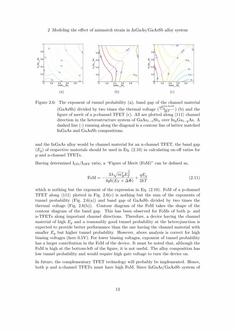
(GaAsSb) divided by two times the thermal voltage (qEGaAsSb
g
2kT ) (b) and thefigure of merit of a p-channel TFET (c). All are plotted along 〈111〉 channeldirection in the heterostructure system of GaAs1−xSbx over InyGa1−yAs. Adashed line (-) running along the diagonal is a contour line of lattice matchedInGaAs and GaAsSb compositions.
and the InGaAs alloy would be channel material for an n-channel TFET, the band gap(Eg) of respective materials should be used in Eq. (2.10) in calculating on-off ratios forp and n-channel TFETs.
Having determined ION/IOFF ratio, a “Figure of Merit (FoM)” can be defined as,
FoM = −3λ
√m∗RE
32T
4qh(ET + ∆Φ)+qEg
2kT(2.11)
which is nothing but the exponent of the expression in Eq. (2.10). FoM of a p-channelTFET along 〈111〉 plotted in Fig. 2.6(c) is nothing but the sum of the exponents oftunnel probability (Fig. 2.6(a)) and band gap of GaAsSb divided by two times thethermal voltage (Fig. 2.6(b)). Contour diagram of the FoM takes the shape of thecontour diagram of the band gap. This has been observed for FoMs of both p- andn-TFETs along important channel directions. Therefore, a device having the channelmaterial of high Eg and a reasonably good tunnel probability at the heterojunction isexpected to provide better performance than the one having the channel material withsmaller Eg but higher tunnel probability. However, above analysis is correct for highbiasing voltages (here 0.5V). For lower biasing voltages, exponent of tunnel probabilityhas a larger contribution in the FoM of the device. It must be noted that, although theFoM is high at the bottom-left of the figure, it is not useful. The alloy composition haslow tunnel probability and would require high gate voltage to turn the device on.
In future, the complementary TFET technology will probably be implemented. Hence,both p and n-channel TFETs must have high FoM. Since InGaAs/GaAsSb system of
13

2 Modeling the effect of mismatch strain in InGaAs/GaAsSb alloy system
7.5
10
12.5
15
17.5
205
7.5
10
12.5
12.5
12.5
12.5
15
15
15
17.5
20
GaAs1−x
Sbx
InyG
a1−
yA
s
0 0.2 0.4 0.6 0.8 10
0.2
0.4
0.6
0.8
1
(a) 〈001〉
7.5 7.5
10
12.5
1517.5
20
5
7.5
10
10
12.5
12.5
12.5
12.5
15
15
15
17.5
20
GaAs1−x
Sbx
InyG
a1−
yA
s
0 0.2 0.4 0.6 0.8 10
0.2
0.4
0.6
0.8
1
(b) 〈110〉
7.5
10
12.5
15
17.5
20
7.5
10
10
12.5
12.5
12.5
12.5
15
15
15
17.5
20
GaAs1−x
Sbx
InyG
a1−
yA
s
0 0.2 0.4 0.6 0.8 10
0.2
0.4
0.6
0.8
1
(c) 〈111〉
Figure 2.7: FoM of p- and n-channel TFETs plotted together along (a) 〈001〉, (b) 〈110〉and (c) 〈111〉 channel direction in a heterostructure system of GaAs1−xSbx
over InyGa1−yAs. For clarity, red labels are used to label the contour linesof the FoM of p-TFET and blue labels are used for the contour lines ofthe FoM of n-TFET. A dotted line running along the diagonal is a contourline of lattice matched InGaAs and GaAsSb compositions. A dashed line atthe top-left of each diagram is a contour line corresponding to zero tunnelprobability. The alloy compositions that could be useful for heterojunctionTFETs are circled in the diagram.
the same alloy composition has to be used for both p and n-channel TFETs, theircompositions must be decided taking the FoMs of both p- and n-channel TFETs intoconsideration. That is, it is necessary to find a single point (x,y) in the contour diagramat which both types of TFETs have large FoM. Fig. 2.7 shows the FoMs of both p- andn-channel TFETs along three important directions. The figure shows a dashed contourat top-right corner corresponding to the compositions that have zero tunnel gap. Thefigure also shows a straight line along the diagonal joining the compositions of latticematched InGaAs and GaAsSb alloys. Comparing the figures, it is observed that thecontours of the FoMs of both n and p-channel TFETs have approximately same shapealong important channel directions. The similarity in the shape of the contour linessuggests that the choice of channel direction will have little impact on the performanceof the TFETs. The regions in the contour diagram that might be relevant for deviceapplications are circled in Fig. 2.7. If the alloy compositions in these regions are selected,the heterostructure TFETs will exhibit high tunnel probability due to smaller tunnelgaps and at the same time low leakage current due to higher band gap. The two alloysare nearly lattice matched in the encircled region. The lattice matching might reducethe interface trap density further reducing leakage currents. A close look at the trendsin the region suggests that increasing Ga mole fraction in InGaAs and As mole fractionin GaAsSb will improve the FoM and ON-OFF ratio in the TFET.
14

2 Modeling the effect of mismatch strain in InGaAs/GaAsSb alloy system
Figure 2.8: Effect of rise in electron Fermi level on tunnel gap and electron barrier.
2.3.4 Limitations of the above analysis
At the end, it must be noted that above analysis is an approximate analysis performedbased on band alignments and effective mass values. It excludes many phenomena thatare important in device operation.
Throughout the analysis, tunnel probability in a TFET is approximated by an expres-sion that is derived for Esaki tunnel diodes. The WKB approximation with a constantreduced effective mass has been used to derive the expression. For more accurate anal-ysis, path integration must be performed along the imaginary k values as given in theKane model [10].
In the analysis, it is indirectly assumed that the Fermi energy in both source and channelwill lie inside the band gaps of respective materials. However, this approximation may beinvalid due to high level of doping. In addition to it, the effective mass and consequentlythe density of states is fairly low in the CB of InGaAs alloy due to which the Fermi levelis expected to rise well above the band edge. As shown in Fig. 2.8, effective tunnel gapis the sum of actual tunnel gap and the electron Fermi level. Therefore, high dopingmight further increase the tunnel gap and reduce tunnel probability. This increase intunnel gap is not uniform throughout the composition range. Additionally, variation instrain throughout the composition will cause variations in the tunnel gap.
In the calculation of ION/IOFF ratio, leakage currents due to trap assisted tunneling areignored. Inclusion of these effects will reduce the ratio.
15

2 Modeling the effect of mismatch strain in InGaAs/GaAsSb alloy system
2.4 Conclusions
In summary, pseudopotential calculations have been performed to determine the effectof strain on the band edges in the InGaAs/GaAsSb heterostructure system. The alloysystem has been analyzed targeting its application for heterojunction TFET devices.The analysis suggests that, it is possible to achieve high tunnel probability in additionto low leakage current.
Considering the driving capacity of target TFET device, which is determined by thetunnel probability, all the directions are equally good throughout the composition range.This is expected, because energy shift in the Γ-valley is affected by hydrostatic strainonly. Since the hydrostatic strain is the same irrespective of growth direction, energyshifts in the Γ-valleys of the CB and VB are approximately same which results in sametrends in the tunnel gaps in important growth directions.
Achieving low leakage currents requires large band gap in the GaAsSb alloy or theInGaAs alloy in a p-channel TFET or a n-channel TFET, respectively. Pseudopotentialcalculations suggest that the alloy range that is circled in Fig. 2.7 would be ideal fora TFET application because of low leakage due to SRH generation currents and hightunnel probability. A close look at the trends in the region suggests that increasing Gamole fraction in InGaAs and As mole fraction in GaAsSb will improve the FoM andON-OFF ratio in the TFET. The calculations also show that the channel direction willhave little impact on the choice of the alloy compositions for TFET applications.
16

Chapter 3Overview of Template Fabrication
Controlled growth of InGaAs nanowires in a predetermined pattern and in cylindricalshape of a fixed redius can be achieved by templated growth technique. Growth ofthe InGaAs/GaAsSb heterostructure system can also be achived using the technique.In this technique, well-like templates of oxide are fabricated over Si substrate. Thebottom of the well is made of crystalline Si on which InGaAs nanowires can nucleateand grow. A brief overview of the fabrication processes is provided in this chapter.Detailed description on the theory and mechanismic aspects of each individual processare explained in subsequent chapters. A detailed description on the fabrication processis given later in Chapter 6.
3.1 Template fabrication process flow
In this fabrication process, a crystalline Si (111) wafer is processed to fabricate oxidetemplates over it. The fabrication process starts with deposition of the oxide on a Siwafer by PECVD using SiH4/N2O chemistry. The oxide layer of 150nm is deposited inthis step. Then, polystyrene nanoparticles with average diameter 100nm are depositedonto the oxide layer. These nanoparticles are used as a mask in the RIE. In this step, theoxide layer is etched by RIE using CHF3/O2 chemistry to form nano-disc-like structureson the wafer surface. Thus, the nanoparticle mask is transferred to the oxide layer. Theoxide nano-disc can now act as a mask in the Si etch step. The purpose of transferringthe nanoparticle mask to the oxide layer is twofolds. Polystyrene nanoparticles aresoft and cannot hold the high intensity plasma that is used in Si etch process. Oxidelayer is relatively hard and can withstand high intensity plasma. Besides, recipes areavailable that can selectively etch Si over oxide. Another reason to transfer the mask isthat, it can improve the thickness of the mask thus allowing more accurate etch of Sinanopillars. The nanoparticle diameter is 100nm. This means the nanoparticle mask is
17

3 Overview of Template Fabrication
at most 100nm thick (vertically). By using proper proportion of CHF3/O2 in RIE, onecan achieve an oxide disc of thickness higher than 100nm.
ICP RIE is used for Si etch with oxide nano-discs as masks. For selective etch of Siover oxide, HBr/O2 chemistry is used. This step yields the Si nano-pillars along withunconsumed oxide mask on their top. The oxide mask is removed and the substrate iscleaned. Then the oxide layer of 150nm thick is deposited on the substrate. The oxidegets deposited on the substrate surface, on the vertical walls of nanopillars and on thetop of the pillars. This layer of oxide forms the template walls in a fully fabricatedtemplate. Therefore, TEOS process is used for the oxide deposition. TEOS processdeposits better quality oxide.
In order to expose the top of Si nanopillar, oxide on the top must be etched keepingthe oxide on the side-walls and the substrate intact. A photoresist is spin-coated on thewafer. It is etched back to expose up the top of the oxide layer capping Si nanopillars.The oxide present on the top of Si nanopillar is then etched by RIE using CHF3/O2
chemistry. Due to anisotropic etching, only the top portion of the oxide pillar getsetched. Oxide on the sidewalls of the nanowires remains unaffected. Due to selectivityof the RIE, the Si nanopillars remain unetched.
The final step in the fabrication of the templates is the wet etch of Si nanopillars tocreate hollow cylinders having oxide walls. This wet etch is performed using tetramethylammonium hydroxide (TMAH). TMAH is a strong base like KOH. TMAH is used in theprocess to ensure compatibility of the process with VLSI processes. A peculiar featureof hxdroxide etch of Si is that the (111) planes of Si show very low etch-rate compared tothe other planes. Since the substrate is a (111) Si wafer, wet etch of vertical nanopillarsinvolves etch along (111) direction. Since (111) planes are removed sequentially duringthe etch, a smooth horizontal surface is formed at the bottom of the nanopillar. Thepillar is not etched completely. This process creates hollow cylindrical templates withthe walls made of oxide and the bottom made of Si substrate. The wafer is then usedfor selective epitaxy of InGaAs inside the template.
18

3 Overview of Template Fabrication
Figure 3.1: Overview of the template fabrication process
19

Chapter 4Brief Description of FabricationProcesses
The etching and deposition processes used in fabrication of the templates are brieflydescribed in this chapter. Throughout this chapter, the name oxide is used in thecontext of Silicon oxide(SiO2).
4.1 Dry Etching Techniques
The etching processes in which etchants are carried to the substrate in gaseous stateare usually referred to as dry etching processes. Dry etching processes carry manyadvantages compared to their wet etching analogues such as high control over etch rate,uniformity over the substrate and reliability of pattern transfer, etc. Most of the wetetching techniques in the industry have been replaced by dry etching techniques. Many ofthe dry etching techniques make use of low pressure plasma for enhancement in etch rateas well as directionality in the etching process[11]. Two versatile dry etching techniques,reactive ion etching (RIE) and inductively coupled plasma-reactive ion etching(ICP-RIE)are explained below.
4.1.1 Principle of reactive ion etching
In Reactive Ion Etching (RIE) technique, a plasma is created between two parallel platesinside the chamber by applying RF voltage across them. The substrate carrying plateis capacitively connected to the source. Capacitive coupling develops DC bias on thesubstrate which increases the bombardment energy and the etch rate. Plasma of anyetching gas contains neutral reactive atoms, positive ions and free radicals. For ex, CF4
20
4 Brief Description of Fabrication Processes
(a) (b)
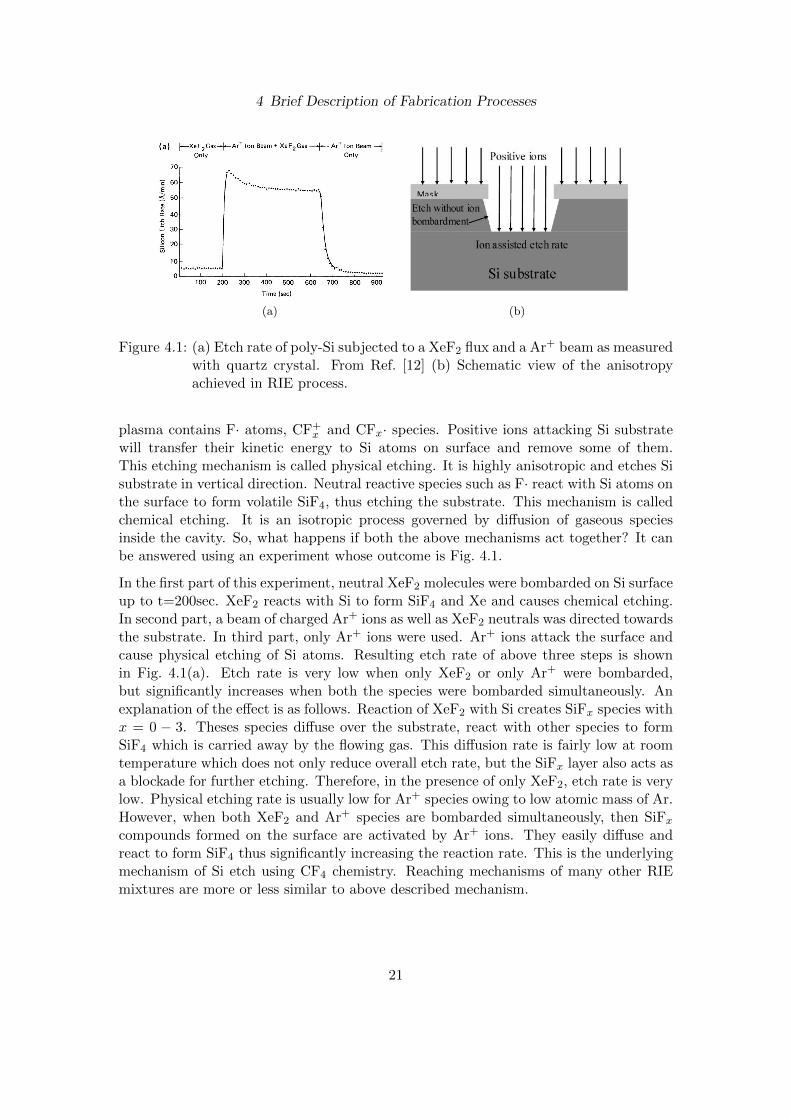
Figure 4.1: (a) Etch rate of poly-Si subjected to a XeF2 flux and a Ar+ beam as measuredwith quartz crystal. From Ref. [12] (b) Schematic view of the anisotropyachieved in RIE process.
plasma contains F· atoms, CF+x and CFx· species. Positive ions attacking Si substrate
will transfer their kinetic energy to Si atoms on surface and remove some of them.This etching mechanism is called physical etching. It is highly anisotropic and etches Sisubstrate in vertical direction. Neutral reactive species such as F· react with Si atoms onthe surface to form volatile SiF4, thus etching the substrate. This mechanism is calledchemical etching. It is an isotropic process governed by diffusion of gaseous speciesinside the cavity. So, what happens if both the above mechanisms act together? It canbe answered using an experiment whose outcome is Fig. 4.1.
In the first part of this experiment, neutral XeF2 molecules were bombarded on Si surfaceup to t=200sec. XeF2 reacts with Si to form SiF4 and Xe and causes chemical etching.In second part, a beam of charged Ar+ ions as well as XeF2 neutrals was directed towardsthe substrate. In third part, only Ar+ ions were used. Ar+ ions attack the surface andcause physical etching of Si atoms. Resulting etch rate of above three steps is shownin Fig. 4.1(a). Etch rate is very low when only XeF2 or only Ar+ were bombarded,but significantly increases when both the species were bombarded simultaneously. Anexplanation of the effect is as follows. Reaction of XeF2 with Si creates SiFx species withx = 0 − 3. Theses species diffuse over the substrate, react with other species to formSiF4 which is carried away by the flowing gas. This diffusion rate is fairly low at roomtemperature which does not only reduce overall etch rate, but the SiFx layer also acts asa blockade for further etching. Therefore, in the presence of only XeF2, etch rate is verylow. Physical etching rate is usually low for Ar+ species owing to low atomic mass of Ar.However, when both XeF2 and Ar+ species are bombarded simultaneously, then SiFx
compounds formed on the surface are activated by Ar+ ions. They easily diffuse andreact to form SiF4 thus significantly increasing the reaction rate. This is the underlyingmechanism of Si etch using CF4 chemistry. Reaching mechanisms of many other RIEmixtures are more or less similar to above described mechanism.
21

4 Brief Description of Fabrication Processes
Above observation shows that, Si etch rate is high only in the presence of both, the Fsupplier species and ion bombardment. In RIE of a vertical trench (as in Fig. 4.1(b)), thebase area is exposed to both reactive F atoms and ion bombardment. It has high etchrate. Although, F atoms get adsorbed on vertical sidewalls, absence of ion bombardmentsignificantly reduces the etch rate. In this way, anisotropy required for fabricating trenchlike structures can be achieved by using RIE[13].
4.1.2 Reactive Ion Etching of oxide
Oxide acts as a mask in many of the VLSI or MEMS device fabrication processes.Usually, a photoresist mask is created on the top of oxide which is deposited on Sisubstrate. To transfer the resist mask onto oxide layer, the oxide must be etched throughresist mask and etching must stop at Si surface to prevent any patterning of Si. Thevertical transfer is achieved by anisotropic RIE technique. Fluorine species can be usedfor the etching of the oxide. These, F· can etch Si surface as well. But the etching muststop at Si surface. That is, the etching recipe and etch mixture must selectively etchoxide over Si. All the above requirements are met if a mixture of CHF3/O2 in the ratio∼50/1 is used in the RIE of oxide. The effect of above mixture is described below.
The CHF3 plasma contains F·, CFx species. Only free fluorine atoms are capable ofetching the oxide. But free F atoms can etch Si as well. Whereas, CFx species do nottake part in any chemical etching step. On the contrary, they react with free F atoms anddecrease effective F concentration. This reduces plasma etch efficiency. Small amount ofoxygen can prevent this side-reaction of CFx with F. Oxygen reacts with CFx species toform COF2 type species and consume CFx. This increases the concentration of F atomswhich in turn increases the etch rate. However, presence of oxygen does not prevent theetching of Si substrate. This is achieved by the presence of H· free radicals in the plasma.H atoms react with CFx species and polymerize them. These polymers get adsorbed onSi surface. Adsorption of the polymers prevents etching of Si by F atoms. Experimentalstudies have shown that these polymers do not get adsorbed on oxide surfaces. Thus,oxide surfaces are still exposed to F atoms and get etched. In this way, highly selectiveetching of oxide can be carried out without affecting Si surface[14].
Although Si surface is blocked from F atoms, the high energy positive ions can penetratethrough soft polymer layer and attack Si surface. This causes damage to Si crystalstructure and induces defects in the crystal. Additionally, the polymers deposited on Sisurface must be removed. This requires special post-process cleaning.
4.1.3 Inductively coupled plasma - reactive ion etching
In many of the new etching processes, the energy of bombarding ions needs to be lowin order to avoid the damage to the surface. Additionally, selectivity of the etchingprocess is high when low energy ions are used for etching. However, in RF capacitively
22

4 Brief Description of Fabrication Processes
coupled plasma RIE, reduction in bombardment energy (i.e. reduction in DC bias) isaccompanied with reduction in plasma density as DC bias is proportional to the plasmadensity. Besides, the etch rate reduces with reduction in the plasma density in RIE.
Inductively Coupled Plasma (ICP) RIE technique is used when relatively high plasmadensity is required in etching process but the ion bombardment energy must be low. InICP-RIE, inductive coils wrapped around the chamber are used to generate plasma bypassing RF current through the coils. Since high voltages are not required to generatehigh plasma density, the plasma potential is low. Thus, low DC bias and high plasmadensity can be achieved using ICP-RIE process. DC bias is tuned by capacitive couplingof the plasma with an RF source. Thus, both bombardment energy of ions as well asetch rate (rate of ion bombardment) can be tuned separately in ICP-RIE.
ICP-RIE is used for anisotropic etching of various materials e.g. Si, Al2O3, GaAs. ICP ispreferred where good quality of the etched surface as well as that of the side-walls needsto be maintained but high etch rate and high anisotropy is required. Si etch using HBrchemistry is a standard etch recipe when the oxide mask is used in pattern transfer. HBrplasma produces atomic Br species which etch Si atoms. Any Group VII elements suchas F, Cl can also be used, but Br etch provide better anisotropy. To improve selectivityof Si to oxide mask, small amount of oxygen is added to the plasma[11].
4.2 Wet Etching Techniques
In etching process, if the etchant is a liquid or is dissolved in a liquid solution, then theprocess is called wet etching. The etchants are usually dissolved in de-ionized water infixed proportion. Wet etching takes place by chemical reaction between etchant speciesand the materials to be etched. Therefore, it is highly selective. It is isotropic, unlessthe reaction kinetics adds certain degree of anisotropy to it. This makes reliable mask-transfer to the substrate difficult. Wet etching rates are usually high and are temperaturedependent. It is difficult to control wet etching process. Non-uniformity of etch-rate overthe wafer is another issue in wet etching process. Due to these drawbacks of wet-etching,many of the wet etch processes are replaced by dry etch processes in VLSI fabricationprocess. Still, wet etch is highly cost-efficient and convenient technique for research scalefabrications. Two wet etching processes that are used in the fabrication of templates aredescribed below.
4.2.1 HF etching of oxide
Hydrogen fluoride etch of oxide is one of the most extensively used chemical etchingprocess in laboratory scale research. It is highly selective to oxide etch and insensitiveto almost all other materials used in fabrication processes including Si. Such a high
23
4 Brief Description of Fabrication Processes
selectivity is achievable at high etch rates close to 120nm/min which is quite impressive.SiO2 undergoes following reaction with HF.
SiO2(s) + 4HF(aq)→ SiF4(g) + 2H2O
Typically, the concentration of HF varies from 1% to 49% in DI water. Increasingconcentration increases etch rate of the solution. To ensure less variability in etch rates,HF is buffered with NH4F typically in the ratio NH4F/HF = 7/1. Etch rate of anygiven oxide film depends on the quality of oxide. Lower etch rate implies better qualityoxide[15].
4.2.2 Hydroxide etch of Silicon
Silicon undergoes oxidation in alkaline solutions to form Si(OH)−24 releasing hydrogen.
These species are soluble in water and are carried away from the reaction site by diffusionprocess. This reaction forms the basis of hydroxide etch of Silicon. The reaction proceedsin two steps.
Step - I: Oxidation of H passivated Si atom on the surface -
Si
SiSi
Si
H
+ H2O + OH− → ≡ Si−OH + H2 + OH−
Step - II: Etching of Si -
Si
SiSi
Si
OH
+ 3H2O→ Si(OH)4 + 3 Si−H
The oxidation step involves the attack of OH− ion on H terminated Si atom to form
unstable Si
SiSi
SiH
OHcomplex. Since Si is pentavalent in this step, it has a high free
energy barrier. Therefore, it is the slowest step among the two. The complex is highlyreactive. It releases unstable H− species which reacts instantaneously with neighbouringH2O molecule to release H2 and OH− ions, thus replenishing consumed OH− ion. In thisway, hydroxide ion acts as a catalyst in the oxidation step and Si-H essentially reactswith water molecules. In next step, oxidized Si atom is released as highly stable Si(OH)−4complex, thus etching Si surface.
24

4 Brief Description of Fabrication Processes
The rate limiting step (oxidation) requires more frequent collision of OH− with Si-Hand the presence of H2O atoms in the vicinity during the collision time. Therefore,higher density of surface Si-H bonds increases the oxidation step rate. Similarly thecondition of presence of H2O in the vicinity demands less steric hindrance from nearbySi-H bonds. Therefore, surface Si-H density should not be too high. Both Si(100) andSi(110) substrates have reasonably good surface Si-H bond density due to which theetch rate along (100) and (110) directions is quite high. However, in the case of Si(111)surface, there are 1 and 3 Si atoms in the alternate layers along every vertical line ina substrate. Therefore, during etching, the S-H bond density is alternately very low orvery high at every site. This significantly reduces etch rate of Si along (111). Hence,etch rate of Si with hydroxide etch is high for (100) and (110) planes and is low for (111)orientation. As a result of anisotropy, hydroxide etches Si rapidly on the any surfaceorientation and stops when it encounters (111) planes. Consequently, different typesof structures with (111) oriented facets are created on the substrates. This effect iscalled faceting. Faceting creates V-grooves in Si (110) substrates or pyramids in Si(100)substrates. Faceting increases surface roughness of the substrate.
Hydroxide etch stops as soon as the etchant encounters oxide surface. Therefore, buriedoxide layer is often used as an etch stop layer in hydroxide etch. Highly p-doped layersare also used as etch stop layers in hydroxide etch. Hydroxide etch practically stopswhen the etchant encounters p+ doped Si surface (in any orientation).
Etch rate of hydroxide etch is temperature dependent. Therefore, it is necessary use ahot water bath to make sure temperature remains constant throughout the etch[16].
4.3 Plasma Enhanced Chemical Vapour Deposition
Chemical Vapour Deposition (CVD) technique is used to deposit a number of thin filmsin microelectronics fabrication industry. Silicon nitride (Si3N4) and oxide (SiO2) aresome of the most used thin films deposited using CVD technique. In CVD, the vapoursof precursor molecules are passed over heated substrate. The precursors get adsorbedand diffuse over the substrate to finally react. For example, silane and N2O are used asprecursors in the deposition of oxide films. However, the process has a drawback. Thesubstrate needs to be heated to high temperatures. In the IC fabrication, oxide is used asa spacer layer between devices and as an insulator for the metal-lines. CVD of oxide atsuch a high temperature could cause damage to metal lines and may as well deterioratedoping profiles in the devices. To avoid high temperature treatment, oxide deposition isperformed using plasma enhanced chemical vapour deposition (PECVD).
In PECVD, a plasma is created in the deposition chamber using RF sources. The plasmagenerates high energy electrons and positive ions which undergo energetic collisions withprecursor molecules and activate or dissociate them. Since precursor molecules are acti-vated before adsorption, they react at lower substrate temperatures up to 300–400.
25

4 Brief Description of Fabrication Processes
(a) (b)
Figure 4.2: SEM view of the cross section of oxide layer deposited by PECVD of silane(a)and TEOS(b). The figure clearly shows the differences in step coverage andconformity of silane and TEOS based processes.
Low temperature processing prevents damage to the prefabricated devices and metal-lines. However, thermally activated reaction and plasma enhanced reaction do not pro-ceed along same reaction paths. That’s why they might yield different products. For ex-ample, plasma enhanced deposition of silicon nitride using silane and ammonia producesSiNH instead of Si3N4 which is produced by thermal CVD. Besides, the properties of thinfilms depend also on the precursor molecules. For example, Tetraethoxysilane (TEOS)and oxygen are also used as precursors in PECVD of oxide. However, the propertiesand the quality of thin films deposited by Silane/N2O chemistry and by TEOS/oxygenchemistry are quite different.
The quality of the oxide depends on its density, stresses present in the oxide. Dense oxideon Si substrate has in-built compressive stress. It also shows high dielectric constantand less interface trap density. Typically the quality of oxide thin films is determinedby its etch rate in HF. Good quality, dense oxide shows low etch rate. The effectivenessof the deposition process is determined by step coverage which is the capacity to fill inthe narrow trenches and vertical walls in Si substrate. Good step coverage is requiredfor the use of these oxides as a dielectric in metal-lines and in trench capacitors.
4.3.1 oxide deposition using Silane
Silane/N2O chemistry is normally used for the deposition of oxide. In this recipe, oxygengas is replaced by N2O to avoid gas phase reaction between released H2 and incoming O2
as the dryness of thin film is essential for device processing. The depositing is performedon Si substrate at 300using high frequency (HF) plasma. The deposition proceeds viafollowing reaction,
SiH4(g) + 2 N2O(g)300oC−−−−→ SiO2(s) + 2 H2(g) + 2 N2(g)
26

4 Brief Description of Fabrication Processes
Due to the absence of H2O as a byproduct, the oxide produced by silane/N2O is adry oxide. However, PECVD of silane does not show good step coverage, conformityand good gap-filling capacity. This is a result of high reactivity of silane which resultsinto gas phase reaction between silane and N2O (or oxygen). Gas-phase nucleated SiO2
particles land on flat surfaces more easily. Surface migration capacity of these particlesis low. Besides, due to high reactivity, adsorbed silane molecules undergo pyrolysis andoxidation fast which results in low surface migration of silane. These effects result intolow step coverage and conformity. The step coverage using silane chemistry is shownin fig. 4.2(a). This gas-phase nucleation is almost impossible to eradicate. Still, due todry nature of oxide films, silane is still used in fabrication. Silane deposited oxide filmsshow high compressive stress. But, the oxide is less dense compared to that of TEOS.HF etch rate is relatively high.
4.3.2 oxide deposition using TEOS
For good step coverage and gap-filling, TEOS is used as a precursor instead of silane.TEOS is in liquid state at room temperature. It is transported to the chamber bybubbling Ar gas through TEOS container. TEOS is deposited at a substrate temperatureof 400using low frequency (LF) plasma deposition. The reaction is as follows,
Si(OC2H5)(g) + 6O2(g)400−−−→ SiO2(s) + 10 H2O(g) + 8 CO2(g)
Si in TEOS is in oxidized form. Therefore, formation of oxide from TEOS is a decom-position and molecular rearrangement reaction. TEOS is not as reactive as silane andtherefore does not cause gas-phase nucleation. Owing to low reactivity, adsorbed TEOSmolecules do not decompose readily into SiO2 leading to surface migration over largedistance. Therefore, the deposited SiO2 shows high step coverage and gap-filling capac-ity. The step coverage using TEOS is shown in fig. 4.2(b). However, during the process,water vapour gets trapped into deposited SiO2 which lowers the quality of TEOS. Hightemperature (> 750) treatment of the oxide removes all the water vapour as well as–OH bonds. Low frequency TEOS deposition produces oxide films with compressivestress. But a combination of low and high frequencies can produce stress free oxidedeposition.
4.3.3 Rapid Thermal Processing
As-deposited oxide layer is often treated with high temperature annealing at 750–800 for short period in oxygen atmosphere. Heating amorphous oxide at high temper-ature releases all the trapped water molecules and trapped –OH groups. It also increasesthe density of oxide layer and improves its stoichiometry.
27

Chapter 5Heteroepitaxial growth of InGaAs -Theory
InGaAs has been an attractive material for semiconductor industry because of its prop-erties such as direct band gap, tunability of the band gap, high carrier mobility, etc.which are superior to those of Si. However, a well developed fabrication technology is amajor advantage for Si based electronics. Integrating InGaAs in Si CMOS technologywould make best use of both these advantages. Therefore, integration of InGaAs ma-terial in Si CMOS technology has been one of the major fields of research. Epitaxialgrowth of InGaAs on Si substrate is an integral step in the integration of InGaAs on Si.Epitaxial growth of InGaAs on Si, the effect of mismatch strain, and in the end, growthof InGaAs nanowires on Si substrate by selective epitaxy are discussed below.
5.1 Epitaxial growth of InGaAs
High quality crystalline InGaAs alloy is required for tunnel FET applications, as lowquality materials have many crystal defects which act as recombination centers andscattering centers. It is possible to obtain high quality crystalline InGaAs by epitaxialgrowth of InGaAs over Si substrate. The process of epitaxial growth will be discussedhere.
5.1.1 Methods of epitaxial growth
Epitaxy is a process of depositing crystalline layer of a material over a crystalline sub-strate. Different techniques of epitaxial growth are available for epitaxial growth such asLiquid Phase Epitaxy (LPE), Molecular Beam Epitaxy (MBE), Metal Organic Vapour
28

5 Heteroepitaxial growth of InGaAs - Theory
Phase Epitaxy (MOVPE), etc. In LPE, the substrate is brought in contact with theprecursors which are present in liquid solution in dissolved form at high temperature.Temperature of the solution is gradually reduced to cause supersaturation of precursorelements in the solution. The excessive elements get epitaxially deposited in the form ofIII-V compounds onto the substrate. LPE is a near equilibrium growth process. WithLPE, it is difficult to control the growth rate and to achieve uniformity in thickness ofgrown material. In MBE, sources of Group III and Group V elements are evaporated ata controlled rate onto a heated substrate under ultra-high vacuum conditions. At lowgrowth rates, the resulting layer is epitaxial. The growth of epitaxial layers occurs out ofequilibrium. The composition of the epitaxially grown layer is controlled by mass-flowrates. With MBE, it is possible to grow atomistically abrupt heterojunctions which isdifficult to achieve with LPE. Although the growth in MBE is highly controlled, the pro-cess is not industry scalable process due to low growth rate, low throughput and highenergy requirement for ultrahigh vacuum. In MOVPE, organometallic compounds ofGroup III elements and hydrides of group V elements are flown over a heated substrate.They react with each other and get deposited onto the substrate. With MOVPE, it ispossible to grow nearly abrupt heterojunctions. Among above three processes, MOVPEis both highly controllable and industry scalable growth technique.
Since MOVPE process is used for the growth of InGaAs nanowires, it is explained herein detail. In MOVPE process, the Group III (In, Ga) and Group V (As) elements arebrought into the chamber in the form of organometallic compounds and hydrides, re-spectively. Organometallics, Trimethyl-indium (TMIn) and Trimethyl-gallium (TMGa)are typically used as precursors of In and Ga respectively. Tertiarybutyl-arsine (TBA -T-ButAsH2) is used as a source for Group V element - As. The substrate is maintainedat high temperature (close to 600). Due to high temperature at the surface of thesubstrate, these precursors undergo pyrolysis in the absence of oxygen which generateselemental Group III atoms and Group V molecules. These species then adsorb ontothe surface, react and get deposited in the form of III-V compounds. Organometallicprecursors are usually used in liquid state. They are carried to the chamber by passinghydrogen through the precursor container and then to the chamber. For the growth ofIII-V compounds, high V/III ratios are used. This means excessive Group V hydrides areflown into the chamber. Under these conditions, the mole fraction of In in InxGa1−xAs isnearly same as the ratio of flow rate of respective precursor molecules. A stable laminarflow is maintained inside the chamber to ensure constant partial pressure of precursorsabove the substrate and that they do not react in gas phase. It also allows the growthof nearly abrupt heterojunctions. Flow rate of precursor molecules is controlled by thevalve and an ultrasonic sensor based feedback system which monitors the density ofprecursor molecules in the flowing hydrogen and feeds it back to the valve controllingsystem.
29

5 Heteroepitaxial growth of InGaAs - Theory
5.1.2 Growth Mechanism of InGaAs in MOVPE
Before studying growth mechanism of InGaAs alloy, we focus on the growth of InAsfirst. For InAs growth, the precursors, diluted TMIn and TBA are passed over heatedsubstrate. Due to high substrate temperature, the molecules undergo pyrolysis. Pyrol-ysis reaction is complete at high temperatures that are used in MOVPE growth. Someof the In atoms released in above reaction get adsorbed onto the surface and developequilibrium with the remaining gas phase atoms. Gaseous As atoms form equilibriumamounts of As2 and As4 species just above the surface. Some of them get adsorbed ontothe surface. Remaining step is the reaction between In and As2/As4 species to yieldInAs which proceeds as follows.
In(g) +1
2As2(g) InAs(s)
In(g) +1
4As4(g) InAs(s)
Above reactions occur near equilibrium or far from equilibrium depending on the condi-tions of the growth, in particular, the growth temperature. At very high growth temper-ature, the above reactions occur near equilibrium and are controlled by thermodynamics.Since the reactions are exothermic (negative enthalpy change), increasing temperaturetends to shift the equilibrium towards reactants (decomposition of InAs). Therefore, therate of formation of the product decreases with increasing temperature. However, hightemperatures are seldom employed for InGaAs growth due to lower growth rate.
Above analysis is a thermodynamics based analysis as it is implicitly assumed that theforward and backward reaction rates are high to ensure equilibrium. Forward reactionrate depends on how fast the reactant species meet each other on the surface and react.As the reaction is exothermic, at low temperatures the equilibrium is towards productside. This means as soon as reactants are available, they are consumed to form product(so as to keep equilibrium balance). Under such conditions, availability of reactants be-comes important. Since low pressure and continuous flow is maintained in the chamber,gas phase reaction between In and As almost never occurs (probability of collision ofgaseous molecules is very low). All the InAs is produced by surface diffusion of In andAs atoms. At low temperature, surface diffusion coefficients of the atoms are low. Inand As atoms are not readily available to reach equilibrium. Therefore, surface diffusionrate determines the rate of reaction. This regime is called kinetically controlled regime.Surface diffusion rate depends on the properties of surface, type of structures present onthe surface, etc. which is not under process designer’s control. Therefore, it is useful tomake sure that the reaction is not determined by surface kinetics.
In above analysis based on surface kinetics, it was assumed that the adsorption rate of Inand As atoms is high. At intermediate temperatures, surface diffusion rate is high andthermodynamic equilibrium is towards product side. Under such conditions, the rateof adsorption of In and As atoms at the interface determines the rate of reaction (and
30

5 Heteroepitaxial growth of InGaAs - Theory
growth rate). This rate is determined by the flux of the species, In and As2, towardsthe interface. Since V/III ratio is 1, In is nearly depleted at the interface. Therefore,piIn p∗In where p∗In and piIn are partial pressures of In atoms in the input gas phaseand at the interface. Since As species are present in excess, consumption of As duringthe growth does not change their partial pressure. The flow of In atoms is the ratedetermining flux in this case. Flux of In species towards the interface is determined bydiffusion equation,
J =DIn ∗ (p∗In − piIn)
RTδ0(5.1)
where DIn is diffusion coefficient of gaseous In and δ0 is the thickness of boundary layerover which Ga partial pressure drops to zero. This flux is directly proportional to thepartial pressure of In in input gas phase. Therefore, growth rate is usually proportionalto the partial pressure of Group III element (or its precursor) in incoming flow. Thisregime is called mass transport controlled regime.
In this way, there are three distinct growth regimes viz. growth controlled by surfacekinetics, by mass transport or by thermodynamics. At lower temperature, surface kinet-ics controls the growth. As surface diffusion rate increases with increasing temperature,growth rate increases with substrate temperature in this regime. At intermediate tem-peratures, mass transport of reactant species towards the surface controls the grow ofInAs. Mass transport coefficient (DIn
RT ) of reactant species is more or less independent ofthe temperature. Therefore, increasing substrate temperature has no effect on growthrate in this regime. At high temperatures thermodynamic equilibrium condition con-trols the growth. In this case, increasing temperature reduces the driving force for thecompletion of reaction. Therefore, growth rate is reduced with temperature. Thus, thetemperature dependence of growth rate can provide insights about the growth regimes.
Growth of InGaAs follows a similar mechanism. Growth of InGaAs alloys is achievedby mixing the precursors of both In and Ga before flowing them into MOVPE chamber.Typically, Trimethyl Gallium (TMGa) is used as a precursor for Ga. V/III ratio ismaintained 1. When substrate temperature is in intermediate range (550to 600),the growth is in the mass flow controlled regime. Therefore, flux of In and Ga atomstowards the substrate will determine the growth rate. Additionally, the mole fractionof In in the alloy InGaAs will be determined by the ratio of flux of In and Ga atoms.Flux is proportional to mass-transport coefficient. Therefore, mole fraction in the solidis given by,
x =JA
JA + JB=
DA · p∗ADA · p∗A +DB · p∗B
(5.2)
When two coefficients are approximately equal, the concentration of In to Ga in solid isequal to the ratio of partial pressures of In and Ga at that temperature.
31

5 Heteroepitaxial growth of InGaAs - Theory
5.2 Heteroepitaxy of InGaAs on Si
Heteroepitaxy is the epitaxial growth of one material on a different material with thesame or different crystal structure. Since the epitaxial material needs to be depositedon a foreign surface, the growth is initiated via nucleation of the new material to coverthe exposed surface the substrate. Mechanism of nucleation and growth mechanismsare explained below in brief. The growth of InGaAs nanowires in well-like Silicon oxidetemplates occurs selectively on exposed Si surface at the bottom of the template. Thepresence of template affects the growth rate as well as the properties of nanowires. Thiseffect is also discussed at the end.
5.2.1 Nucleation and growth of InGaAs over Si
Consider the case of nucleation in homo-epitaxy (that is the epitaxial growth of a materialon the substrate of same material) using VPE technique. Supersaturation of the vaporover the substrate is a necessary condition for vapor phase epitaxy. Free energy changeper unit volume due to the nucleation is given by ∆Gv = −nkT lnP0/Peq where P0 isactual partial pressure and Peq is the equilibrium partial pressure of the reactant species.In addition to it, there is a surface energy associated with the exposed surface of thenucleus. Total energy change when a nucleus of radius r is formed from gaseous reactantsis given by,
∆G = −4πr3
3nkT lnP0/Peq + 4πr2γs (5.3)
where γs is surface energy of the nucleating material. Above equation shows that, ∆Gis negative for a certain nucleus radius r > rcrit. Therefore, the nuclei with r > rcrit willcontinue growth by accumulation of more and more material while those with r < rcritwill disappear due to re-evaporation of atoms (as it is favorable for these nuclei). Anucleation rate can be determined using above thermodynamic analysis. But more im-portantly, eq. 5.3 shows that the nucleation rate strongly depends on supersaturation(P0) and on nucleation temperature. In the case of heterogeneous nucleation, when epi-taxial and substrate material are different, the nuclei “wet” the surface of the substrate.In this case, the effect of surface energies of both epitaxial layer (γe) and substrate (γs)along with the interface energy between substrate and epitaxial material (γi) must beconsidered in calculating free energy change. When γi > γe +γs, then the epitaxial layerwill not wet the substrate, whereas if γs > γi + γe, then the nuclei can fully wet thesubstrate. For all intermediate case, the nuclei will wet the surface with a particularwetting angle. Free energy change in this case can be calculated by including the effectof partial or full wetting. In the case of the growth of InGaAs on Si, InGaAs is polarwhile Si is non-polar, therefore the interface energy will be quite high and InGaAs willonly partially wet Si surface. Therefore, high supersaturation or low temperature willbe required for proper nucleation of InGaAs on Si.
32

5 Heteroepitaxial growth of InGaAs - Theory
Once nucleation is achieved, growth proceeds via expansion and coalescence of the nucle-ated islands. When there is low mismatch strain, deposition at island boundaries is morefavorable as the atom depositing at the boundaries can form bonds with two surfaces(substrate and vertical wall of island). In this case, adsorbed atoms of epitaxial materialdiffuse to the boundaries of the islands and get deposited there. However, if mismatchstrain is high, then adsorbed atoms will climb the island walls at the boundaries andwill deposit onto the terraces (i.e. island surfaces) as the mismatch strain is low overthere. In such case, the islands will grow vertically and form three dimensional struc-tures before they coalesce at their base. Discrete trapezoidal structures are formed inthis mode. This mode is called Volmer-Weber (VW) growth mode. In the heteroepitaxyof InGaAs over Si, the high mismatch strain causes the epitaxial growth of InGaAs overSi to follow VW growth mode which results into small islands over a large substrate.But, in templated growth of InGaAs nanowires, the growth takes place over a smallisland of Si. This might affect the growth mode.
5.2.2 Effect of Si surface
Silicon is a nonpolar semiconductor while InGaAs is a polar semiconductor. Along (111)planes, zinc blende crystals of InGaAs can be considered as made of alternate layers ofnegatively polar As and positively polar In/Ga atoms stacked one over another. In theheteroepitaxy of InGaAs on Si (111) surface, different islands can nucleate with either Astermination on Si or In/Ga termination on Si. When such islands meet, inversion domainboundaries (IDB) are formed at their joints. Such boundaries can act as recombinationcenters and must be avoided. That’s why, before the nucleation event, Si surface ispassivated with As by passing TBA over Si. This treatment removes IDBs. IDBs canalso be caused due to monoatomic steps on the surface arising due to miscuts. As shownin figure. 5.1, monoatomic surface steps can give rise to IDBs but diatomic steps donot result into IDBs. Si surface can be made free of monoatomic steps by annealing Sisubstrates in hydrogen.
Sometimes surface steps are deliberately introduced by miscuts. This is because, theedges of surface steps act as nucleation centers. As the steps are uniformly placed allover the surface, the nucleation takes place uniformly and nucleating layer covers entirearea.
5.2.3 Effect of strain
There is a lattice mismatch of minimum 4% (pure GaAs) to maximum 11% (pure InAs)when these materials are epitaxially grown on Si substrate. Lattice mismatch will varylinearly between the above two values in case of epitaxial growth of InGaAs on Si. Thislattice mismatch results into a compressive strain in the epitaxially grown layer. Strain
33

5 Heteroepitaxial growth of InGaAs - Theory
(a) (b)
Figure 5.1: Effect of monoatomic steps(a) and of diatomic steps(b) in nonpolar Si sub-strate on the growth of polar epitaxial layer of III-V materials
in the epitaxial layer might even affect the composition of epitaxially grown InGaAs, asexplained below.
Consider a situation in which the growth conditions constrain Ga mole fraction ingrowing InGaAs to be 0.5. This means that the chemical free energy is minimumfor In0.5Ga0.5As under such conditions. Presence of stain increases free energy of theIn0.5Ga0.5As/Si system. One way of reducing this strain energy is to change the com-position of the epitaxial layer. Increasing Ga mole fraction above 0.5 would reduce themismatch strain and consequently reduce the strain energy during the growth. How-ever, this would increase the chemical free energy (it is minimum for In0.5Ga0.5As).Therefore, total(strain + chemical) free energy of the system could have a minimumat xGa > 0.5. Such a reduction in strain energy is achieved at the cost of increase inchemical potential energy of the growth process. Since In and Ga are highly volatile athigh temperatures, such a change in composition is brought by rapid evaporation of Inin relation to Ga. Thus, the mismatch strain between epitaxial layer and substrate canaffect the composition of alloys.
Strain relaxation can take place in the InGaAs crystal by introducing crystal defects. Thecrystal defects are detrimental for the device performance. Therefore, lattice mismatchedheterostructure systems are preferred due to less number of crystal defects.
5.3 Templated growth of InGaAs nanowires
In selective epitaxy of InGaAs on Si(111) surface[17], the surface of the wafer is coveredwith amorphous Silicon oxide. The pits where InGaAs nanowire is to be grown areexposed by etching oxide on their top. When such a patterned wafer processed inMOVPE, InGaAs nanowires get nucleated only on exposed Si surface. This is because,
34

5 Heteroepitaxial growth of InGaAs - Theory
(a) (b)
Figure 5.2: A schematic diagram showing InGaAs nanowire growth by selective epitaxyof InGaAs in the pits on patterned Si substrate
epitaxial growth requires the substrate surface to be crystalline. InGaAs nucleationand growth takes place only on Si surface inside the template. Even if any InGaAsnucleates on the field oxide, it gets re-evaporated owing to high substrate temperature.A schematic view of the growth using epitaxy is shown in fig. 5.2. The flat top is madeof (111)InGaAs while the vertical surfaces are made of (110)InGaAs and equivalentplanes. Since (110) surfaces are highly stable, the growth rate along 〈111〉 is much highercompared to that along 〈110〉. This preferential growth along 〈111〉 results into a flattopped, vertical nanowire. A major drawback of this method of InGaAs nanowire growthis the lateral growth of InGaAs. Since the growth rate along 〈110〉 is not completelyzero, lateral growth is also observed. If Si (110) or Si (001) is used in epitaxy, growthrate of (111)B facets of InGaAs is so high that most of the nanowires grow inclined tothe substrate.
To overcome the drawbacks of above described process, growth of InGaAs nanowire onSi substrate is achieved by selective epitaxy in a well-like Silicon oxide template[18]. Inthis method, well-like SiO2 templates having crystalline Si surface (schematically shownin fig. 5.3) at the bottom are created. Rest of the Si surface is covered with amorphousSiO2. InGaAs nucleation and growth takes place on exposed Si inside the template.Template walls provide physical confinement due to which InGaAs nanowires do notgrow laterally even if Si (110) or Si (001) substrates are used. Oxide templates can beeasily removed by wet etching of SiO2 in HF solution.
InGaAs nanowires are grown in the oxide template at high temperature. The nanowiresare sufficiently tall to relieve lattice mismatch stress due to substrate. Therefore, as-grown nanowires are relaxed. However, when the wafer is cooled down to room tempera-ture, these nanowires might develop lateral stress owing to the differences in the thermal
35

5 Heteroepitaxial growth of InGaAs - Theory
(a) (b)
Figure 5.3: A schematic diagram showing template based growth of InGaAs nanowireson Si substrates
expansion coefficients of oxide template and InGaAs material. But it is quite uncertainand needs to be experimentally verified.
36

Chapter 6Templated Growth of InGaAs Nanowires
Fabrication of the templates involves processing of an Si wafer through a number ofsteps. The process flow to fabricate the templates on the Si wafer is briefly explained inChapter 3. The oxide templates were fabricated using the process flow. The fabricationprocess of the templates is described below. Growth of InGaAs nanowires by MOVPEis described at the end of the chapter.
6.1 Fabrication of Silicon Nanopillars
Process steps to fabricate Si nanopillars from a Si wafer are explained in detail in thissection.
6.1.1 Nanoparticle Mask Preparation
Since the nanoparticle mask is going to be transferred to the oxide layer underneath it,oxide must be deposited before nanoparticle deposition. Silicon oxide layer of 150nmthickness is deposited onto the Si(111) substrate by PECVD using SiH4/N2O chemistry.Oxford PlasmaPro 100 PECVD instrument is used for the process. The deposition iscarried at the chamber pressure of 1000mTorr, RF plasma power of 20W and SiH4/N2Oratio of 720/150. Substrate is heated to 300. Under above conditions, SiO2 depositionrate is 43nm/min. The step coverage is found to be 150nm/75nm. Silane based oxideis a low quality, low density oxide. However, since the oxide is used only as a mask, thequality of the oxide would not affect the device. Therefore, low cost silane oxide is used.Oxide layer thickness was varied from 110nm to 200nm to check if oxide layer thicknesschanges the thickness of the oxide mask. Based on the observations, the thickness of theoxide layer was fixed to 150nm.
37

6 Templated Growth of InGaAs Nanowires
Polystyrene nanoparticles are used as a mask. A solution containing polystyrene nanopar-ticles in colloidal form is diluted to 3.3× 10⁻³w/w to achieve desired nanopillar densityon the substrate. The solution is then dropped and spread onto the substrate using apipette. To ensure adhesion of the nanoparticles on the oxide surface, the wafer is coatedwith a thin layer of Poly-L-Lysine before nanoparticle deposition. After the deposition,the wafer is rinsed with DI water and dried with Nitrogen gun.
6.1.2 RIE - Transfer of nanoparticle mask to oxide
In order to obtain hard mask, the nanoparticle mask is transferred to the oxide layerby RIE using CHF3/O2 chemistry. Oxford NPG 80 RIE instrument is used for theetch. The etching is performed using 100W of RF plasma power and chamber pressureof 13.3 mTorr. Under these conditions the RIE gives an etch rate of 16nm/min. TheRF power could have been increased to 300W or more to increase the etch rate, butthe selectivity is low under high power conditions. Selectivity is the ratio of oxide etchrate to the polystyrene nanoparticle etch rate. Higher the selectivity, thicker the oxidemask that we get out of RIE. Under low power conditions, the etching is mainly achemical etching of the oxide caused by F· atoms in the plasma. The F· atoms do notetch polystyrene. Therefore, etch selectivity is high under low power condition. Usuallysmall amount of oxygen is added to the plasma to increase the F· concentration and theetch rate. As a side effect, this oxygen reacts with polystyrene and etches it. As a result,addition of oxygen reduces the selectivity of the etch process. In order to obtain optimaloxygen pressure, O2/CHF3 ratio was decreased from 1/49(standard ratio) to 0/49 andthe thickness of oxide mask was checked. The scanning electron microscope(SEM) imagesof the final oxide mask for different O2/CHF3 ratios are given in Fig. 6.1. Based on theobservations, it was decided to use the O2/CHF3 ratio of 0/49 (i.e. no oxygen flow).
Close look at the images in Fig. 6.1 will reveal that the oxide mask obtained fromthe nanoparticles is trapezoidal. This is probably an effect of the spherical shape ofthe nanoparticles. The vertical thickness of the nanoparticles is not constant, but is afunction of the distance from the center of the sphere. It is given by,
t⊥ = 2 ∗√R2 − x2 − y2 (6.1)
where R is the radius of the nanoparticle and x, y are the space coordinates. Eachnanoparticle mask is thicker at the center (x2 + y2 = 0) and thinner around the periph-ery. The material at the periphery will be etched out earlier than that at the centralregion, thus allowing the ions to attack the oxide beneath it. Therefore, oxide below theperiphery of the mask gets etched more compared to that below the center. This resultsinto a trapezoidal shape of the oxide etched from the nanoparticle mask. It may alsobe possible that soft polystyrene ball melts or deforms due to persistent attack of theenergetic ions. But, no such study is made to check this possibility.
38

6 Templated Growth of InGaAs Nanowires
(a) O2/CHF3 = 2.0% (b) O2/CHF3 = 1.4% (c) O2/CHF3 = 1.0%
(d) O2/CHF3 = 0.3% (e) O2/CHF3 = 0.0%
Figure 6.1: Optimization of RIE process by varying O2/CHF3 gas flow ratio into theRIE chamber. Images of the oxide mask taken using SEM are shown above.All the images are taken at 300 tilt and have the same scale. Reduction ofoxygen in the gas flow increases the height of the oxide mask etched.
(a) O2 = 1.5sccm (b) O2 = 1.7sccm (c) O2 = 1.9sccm (d) O2 = 2.0sccm (e) Varying O2 flow
Figure 6.2: Determining optimal ratio of flow rates of O2 and HBr into ICP chamber. (a-d) Four different samples were etched with different O2 flow rates. A constantO2 flow was maintained throughout the etch. (e) Oxygen flow rate was variedin-situ from 2.1sccm to 1.3sccm during the etch of a single sample. In allthe etch recipes, the HBr flow was kept constant at 51sccm. The nanowireetched with varying O2 flow is less tapered than the nanowires etched withconstant oxygen flow.
39

6 Templated Growth of InGaAs Nanowires
The CHF3 plasma contains different species ranging from F·, CF2·, CHF·, etc. Thesespecies form polymers and get deposited on Si substrate. These polymers must beremoved to avoid contamination in further processing. Removal of these polymers andother “etch residues” is done by “EKC 265”. The solution is heated to 90 and RIEtreated Si wafer is dipped into it for 30min for effective removal of the etch residues.
A short Rapid thermal Annealing (RTA) process was introduced after RIE etch andcleaning. The purpose of RTA is to densify and strengthen the oxide mask. The testscarried out earlier confirmed that RTA in both Forming gas or oxygen atmosphere im-proves the quality of the PECVD deposited oxide. It was expected that, a stronger oxidemask would be more resistant to the etch in ICP RIE. It would therefore offer higher se-lectivity in Si etch. RTA was carried out at 750for 30sec either in Forming gas(Ar/H2)atmosphere or in oxygen atmosphere. However, the results were not so promising. Theshape of the nanowires etched in ICP were approximately same irrespective of whetherthe mask is RTA processed or not. Therefore, the RTA step after RIE was skipped innext samples.
6.1.3 ICP RIE - Fabrication of Si nanopillars
In this step, the Si substrate is etched up to 1µm depth with the oxide nano-discs as amask. The etch results into formation of Si nanopillars on the wafer surface where thenanoparticles are present. The etch is carried out using Oxford NPG 100 instrumentand HBr/O2 chemistry is used. It is performed at the chamber pressure of 3.9-4.0mTorr,ICP power of 350W, RF power of 90W and substrate is heated to 50. This step is themost crucial step in template fabrication process as this step determines the shape ofthe nanopillars and their depth.
The HBr/O2 chemistry is selected to achieve high selectivity in Si etch over SiO2. TheBr· free radicals are responsible for Si etch. Br· radicals react with Si atoms on the surfaceto form SiBr4 compounds which are then carried away. Fluorine or Chlorine undergothe same reaction with Si, but F· and Cl· etch is more isotropic which results into highunderetch. Therefore, Br· is chosen. However, Br· etches oxide as well which results intolow etch selectivity. The etch selectivity can be improved by adding small amount ofoxygen into the plasma. The ratio of HBr/O2 flow rate is determined accordingly.
The etch recipe consists of two steps. In the first step, the native oxide on Si surface isremoved by a short etch with only HBr under the same chamber condition as the mainetch step. Oxide breakthrough is carried out for 30sec. A small amount of oxygen isthen added to HBr to achieve high selectivity in Si etch.
Addition of oxygen to the plasma has a negative side-effect. Si etch with HBr only recipeproduces SiBr4 which is carried away. However, addition of oxygen produces smallamounts of SiOBr2 products which get deposited on the side-walls of the nanopillarsbeing etched. These SiOBr products act as a mask for further etch of Si below. Constantredeposition of SiOBr products causes sidewalls of the nanopillars slanted outwards.
40

6 Templated Growth of InGaAs Nanowires
That is, the diameter at the bottom of the pillar is larger than that at the top. Thetemplates made from such slanted pillars are “cone shaped” instead of cylindrical. Themore the oxygen content in HBr, the more slanted the etch profiles are. Therefore, anoptimal value of HBr/O2 ratio must be used to achieve nearly vertical sidewalls and highselectivity.
There is an additional complication arising from trapezoidal shape of the oxide mask.As the mask is thinner around the periphery, it will get etched before the mask at thecenter. Therefore, Si at the edges will be attacked during the etch if etched for long.The pillars may get overetched at the top. The effect of tapered oxide mask must betaken into account in determining the optimal value of HBr/O2 ratio.
In first part of optimization, oxygen flow to ICP chamber was varied from 1.5sccm to2.0sccm while keeping HBr flow constant at 50sccm. The nanowires obtained by varyingO2 flow are shown in the SEM images in Fig. 6.2. The nanowire etched with minimumoxygen flow is slightly overetched while the nanowires with high oxygen flow rate aretapered. The tapering increases with increasing oxygen flow rate. The experimentshowed that, with no oxygen flow rate can one obtain Si nanowires with no overetchingand vertical sidewalls. In order to achieve both vertical sidewalls and no overetching,oxygen flow was varied in-situ from 2.1sccm to 1.3sccm in four steps during the etch.This resulted into the nanowires with vertical walls and negligible overetching as shownin Fig. 6.2(e).
In the experiments, it is observed that the quality of Si etch depends largely on the historyof usage of the ICP machine. History of usage determines the chamber conditions suchas chamber wall passivation. ICP etch of Si is sensitive to these conditions. Therefore,none of the above described results could be reproduced using the same recipe. Smallchanges in oxygen flow rate had to be done to obtain desired results. This might suggestthat, good quality etching obtained by varying oxygen flow could just be a result of idealchamber conditions at that particular time. Despite of this “history effect”, it is certainthat varying oxygen flow during the etch results into less tapered sidewalls comparedto constant oxygen flow. Therefore, recipe with varied oxygen flow is used to etch thenanowires in next runs.
6.2 Oxide Template Fabrication
Templates are created from Si nanopillars by depositing oxide around the nanopillarsand etching back the pillars. The process is described here in detail.
6.2.1 Deposition of Si Oxide for template walls
As the oxide deposited on the vertical walls is going to form the template walls in a fullyformed template, the oxide must show proper step coverage, conformity and uniform
41

6 Templated Growth of InGaAs Nanowires
coverage at concave and convex corners of the structures on Si substrate. The oxidefor template walls is deposited by PECVD. Two alternatives namely, silane based recipe(SiH4/N2O) and TEOS based recipe (Si(OC2H5)4/O2) are available for oxide deposition.It is known that Silane based recipe deposited oxide has incomplete coverage at concavecorners (such as base of the nanopillar). The oxide deposited on the side walls could bedisconnected from the oxide on the surface which could result into detachment of thetemplates after Si etch. TEOS, on the other hand, due to its low reactivity and in situreflow capability, can deliver uniform oxide coverage even in deep trenches. Therefore,TEOS based recipe is used for oxide deposition.
Since TEOS is in liquid state at room temperature, it is carried to the chamber by bub-bling Ar gas through TEOS vessel. The vessel is heated to 55and the tube carryingTEOS to the chamber is heated to 75to avoid deposition of TEOS inside the tube.The deposition is carried out with RF power of 60W, the chamber pressure of 500mTorrand Ar-TEOS/O2 ratio 500/500*. Substrate is heated to 400before deposition. Un-der these conditions, the deposition rate is 67nm/min on horizontal surface. The stepcoverage is 150nm/85nm. In this step, 150nm TEOS is deposited on the plane surfaceand 85nm oxide is deposited on the sidewalls.
Oxide is deposited on the backside of the wafer to avoid its etch in hydroxide etch step.Silane based oxide deposition recipe is used for the deposition.
6.2.2 Opening the cap on Si nanopillars
To begin with, the wafer is coated with HMDS before spin-coating the photoresist. Then,photoresist AZ1505 is spin-coated on the substrate by rotating the wafer at 4000rpm for40sec. This gave approximately 500nm thick layer of the photoresist. It is followed by asoft bake at 110for 1min. This recipe ensures proper coverage of the photoresist overthe wafer.
Next step etches oxide and reveals the top of Si nanopillars. Anisotropic etch is necessaryin this step because, only the oxide on the top of the pillar must be etched protecting theoxide on sidewalls. Although the photoresist is present up to 500nm above the surface,the nanopillars are 1µm tall. An isotropic etching e.g HF etch will etch the oxide notonly on the top, but also on the sidewalls above the photoresist layer. Therefore, theoxide etch is performed with RIE. The cap opening recipe using RIE consists of threesteps. In the first step, some photoresist which might have been deposited on the oxidelayer at the top of the pillar is removed by RIE in oxygen plasma. In next step, theoxide is etched anisotropically to open the top of the nanopillar. The same recipe asthat used in the nanoparticle mask transfer (CHF3/O2) is used for oxide etch. In thelast step, damaged photoresist on the surface is etched away by RIE in oxygen plasma.The sample is then checked under SEM to make sure all the oxide on the top is indeedetched. SEM images of the substrate are shown in Fig. 6.3.
42

6 Templated Growth of InGaAs Nanowires
(a) (b)
Figure 6.3: SEM images of opened top of Si nanopillar by etching the oxide layer. (a)Top view of the nanopillars. It clearly shows core-shell arrangement with abright Si core and oxide shell. (b) SEM view of 300 tilted nanopillar.
The photoresist left on the surface is then stripped away by dipping the wafer in Acetone,Isopropyl alcohol and DI water for 5min each. Traces of photoresist are still present onthe surface. This is removed by cleaning the sample in piranha. Piranha is a solutionprepared by mixing conc. H2SO4 and H2O2 in the ratio 2:1 at 90. On mixing, both theingredients react to form H2S2O8 which is a highly oxidizing species. It reacts with allthe organic matter in the sample and oxidizes it thus getting rid of the organic material,if any.
6.2.3 Template fabrication
The fabrication steps till now have produced nanopillars with Si core and oxide shell.The diameter of Si core is ∼100nm and the thickness of oxide shell is 85nm. Fabricationof the templates requires etching Si core. This Silicon etch must be highly selective.Therefore, hydroxide etch is used here. To ensure CMOS compatibility, TMAH is usedas a source of hydroxide ions.
A solution of 2% TMAH in DI water is used in the etch. The solution is kept at 66-70 during the etch. Under these conditions, Si etch rate is approximately 40nm/min to50nm/min for (111) oriented Si wafer. Etching Si nanopillars on Si(111) requires an etchalong 〈111〉. Therefore, the etch rate of nanopillars is equal to the hydroxide etch ratealong (111) direction. High variability in hydroxide etch rate is observed. This is becausein hydroxide etch process, the etch rate is sensitive to temperature and hydroxide ionconcentration in the solution. In order to achieve the etch at a constant temperature, thesolution is heated to 85 using hotplate for 30min before starting the etch process. Thebeaker is covered with a lid to avoid evaporation of the water and change in hydroxide
43

6 Templated Growth of InGaAs Nanowires
(a) (b)
Figure 6.4: SEM images of the well-like templates obtained by etching Si nanopillarswith TMAH. (a) SEM image of a template tilted by 30°. (b) SEM imageof another template tilted by 60°. It shows the importance of having Sinanopillars with vertical sidewalls. Nanopillars with tapered sidewall resultinto a “cone” shaped template instead of a cylindrical one.
concentration. Despite these measures, the temperature of the solution is observed tovary between 66-70.
Highly selective hydroxide etches Si surface only and leaves the oxide surface untouched.This creates hollow templates of oxide walls with Si bottom. Fig. 6.4 shows two rep-resentative templates. The templates are ready for InGaAs nanowire growth. Thetemplates are treated with RTA process which involved heating the templates in Form-ing gas (H2/Ar) atmosphere at 750for 30sec. In addition to densifying the oxide, RTAremoves water and OH− ions trapped inside the oxide.
6.3 Epitaxial Growth of InGaAs Nanowires
MOVPE process is used for the epitaxial growth of InGaAs nanowires in the templates.The growth takes place on exposed Si surface inside the template, as epitaxial growthrequires a crystalline substrate for the nucleation. As SiO2 is not crystalline, ideallyno InGaAs growth would be observed outside the template. However, impurities suchas metal atoms, etc. present on oxide surface can act as a catalyst for InGaAs growthresulting in oddly shaped chunks of InGaAs. To avoid such a field growth of InGaAs, thewafer surface must be properly cleaned. Proper cleaning also prevents contamination ofthe MOVPE chamber.
To get rid of any organic dirt, the wafer is cleaned in oxygen plasma. Prolonged exposureto air or cleaning in oxygen plasma develops a thin layer of native oxide on exposed Si
44

6 Templated Growth of InGaAs Nanowires
Table 6.1: Template dimensions. The dimensions listed in the template belong to onesingle template which is a representative of all.
Template Dimensions
Sample IdHeight Base Dia. Top Dia. Aspect ratio Slant
nm nm nm
p13 672 160 125 4.72 0.0260
n11 830 105 96 8.25 0.0054
p14 625 158 128 4.37 0.0240
n13 680 110 105 6.32 0.0037
n12 620 114 110 5.62 0.0032
surface inside the pillar. This thin oxide layer prevents nucleation of the InAs. To etchit away, the wafer is dipped in dilute HF (1:20) for 15sec which etches ∼5nm of thermaloxide. It ensures all the native oxide on the surface has been etched away. As a side-effect, HF dip also etches the template walls and inner diameter of the template increasesby ∼10nm. The template is then rinsed in DI water followed by IPA. Dried templateis immediately transferred into the loadlock of the MOVPE chamber. The transfer tothe loadlock must be quick to ensure minimum oxidation of Si surface and minimumcontamination from the air.
In the MOVPE process, growth rate InGaAs on Si surface depends on different factorswhich include total partial pressure of In and Ga species above the substrate, V/IIIratio, substrate temperature, supersaturation, etc. Additionally, growth rate of InGaAsin a template is different due to the presence of the hollow tube-like template, as thediffusion coefficients of gaseous In, Ga and As species will be altered by the confinement.As a result, growth rate depends also on the template height, base area and aspect ratioof the cylindrical template. The template-specific factors are given in Table 6.1 for eachsample. Variations in the templates from sample to sample are due to variations in theshape of Si nanopillar. Slight variations in the template diameter were observed evenon the same wafer due to differences in nanoparticle size. This may change height ofthe InGaAs nanowires grown in the templates. Local factors, such as local density oftemplates can also influence the size of the nanopillars. The less dense the templates,the taller the InGaAs nanopillars. This is because, if the nanopillars are not dense,then they accumulate adsorbed species of In, Ga, As over a larger area and can growtaller. Cleanliness in a certain area of the sample can also influence the growth rate as itcreates chunks of InGaAs and consumes the material. The samples used for the growthare sufficiently clean that one can ignore the effect of cleanliness on growth rate.
MOVPE growth of InGaAs nanowires begins with the passivation of Si surface with Asatoms. The substrate is heated to 580 and AsH3 is passed over it. AsH3 pyrolyzes
45

6 Templated Growth of InGaAs Nanowires
Table 6.2: Conditions of MOVPE growth for InGaAs nanowires on different samples
MOVPE Growth Conditions
Sample IdTMIn TMGa Total
xvapourGa
Growth Time
µMol/min µMol/min µMol/min minute
p13 2.5 0.24 2.74 0.087 10
n11 2.27 0.48 2.75 0.174 20
p14 2.08 0.67 2.75 0.244 15
n13 1.41 1.35 2.76 0.489 10
n12 0.67 2.09 2.76 0.757 15
and produces As2/As4 which passivate Si surface with As. The passivation ensures that,all the nucleation layers have As termination and avoids inversion domain boundaries inthe crystal. InAs is used as a nucleating layer and as a buffer layer between InGaAs andSi substrate. InAs buffer is grown by passing 2.75µmol/min of TMIn over Si substrateheated to 600 for 5min. This would grow approximately 100nm of InAs. InGaAsnanowire is then grown over InAs buffer layer. The MOVPE growth of InGaAs nanopil-lars is performed by varying the ratio of flow-rates of TMIn and TMGa precursors. Totalflow rate of Group III precursors and the V/III ratio is kept constant in all the growthprocesses to make sure the growth conditions are same for all InGaAs nanowires. Growthconditions for all the samples are given in Table 6.2.
The templates filled with InGaAs are observed under SEM. Fig. 6.5 shows the SEMimages of the templates with completely filled InGaAs and over-grown InGaAs. Boththe images were taken on the same sample at places separated by 460µm. Such avariation could be observed due to local effects such as variations in the template sizeor variations in the template density, etc. which are not under control. Whether thevariations in template size and template density affect Ga mole fraction in the nanopillaris unclear.
To observe the effect of the template on the properties of InGaAs nanopillars (in par-ticular, thermal strain in the nanowires), templates are etched by a dip in buffered HFsolution. The nanopillars are then observed under SEM to have a close look at theirshape. Representative nanopillars on each sample are shown in Fig. 6.6. Almost all thenanopillars on sample p14 were overgrown due to long growth time while on the othersamples (except n11) the templates were half filled on an average. On n11 sample, mostof the templates were filled up to the brim with a few nanopillars overgrown out of thetemplates. Variation in average height of the nanopillars on different samples can be ex-plained by looking at the growth period, nonlinearity in the growth and aspect ratios ofthe nanopillars. The higher the aspect ratio, the lower the growth rate. This also resultsin nonlinearity in growth rate. In the beginning, the growth rate is low as the template is
46

6 Templated Growth of InGaAs Nanowires
(a) (b)
Figure 6.5: (a) A template completely filled with InGaAs nanopillar. (b) A templatewith overgrown InGaAs. SEM images are taken in a 60° tilted view. Theimages are taken on the same sample (Id. n11) at nearby places (which areseparated by 460µm).
unfilled. As the template gets more and more filled, aspect ratio of the structure reducesand growth rate increases substantially. Despite of long growth period of 20min, thetemplates in n11 did not overflow owing to high aspect ratio of the structure. Despite ofhaving same growth period of 15min, the nanopillars in n13 and n12 did not overgrowwhile those in p14 showed heavy overgrowth. This could be attributed to low aspectratio of the latter sample. The effect of Ga mole fraction on the growth rate cannot beassessed here as a variation in shapes and sizes of the templates might overshadow it.
Although the nanopillars shown in Fig. 6.6 have a perfect cylindrical shape with aflat top and smooth sidewalls, plenty of the nanopillars were oddly shaped with somehaving triangular or slanted top, some having incompletely filled cylinders, some showingovergrowth in different (111) directions. These differences can be qualitatively explainedas follows.
The MOVPE conditions used in the growth of InGaAs nanowires had been optimizedfor the growth along 〈111〉B direction. 〈111〉B is 〈111〉 direction with Group V termina-tion. To make sure vertical growth of InGaAs, it is necessary to maximize the growthrate along 〈111〉B. Despite of that, growth along other directions cannot be completelysuppressed.
A nanowire grown predominantly by the growth along 〈110〉 is shown in Fig. 6.7(a). Ithas a triangular pyramidal top made of equivalent (110) planes which might cause if theinitial conditions were more favorable for the growth along (110) direction. A benefitof template-guided growth is that InGaAs growth is confined along 〈111〉 by physicalbarriers which greatly relaxes the requirements for the growth of vertical nanowires.Therefore, despite of favorable conditions for (110) growth, the nanopillar was vertical.
47

6 Templated Growth of InGaAs Nanowires
(a) p13 (xvapourGa =0.08) (b) n11 (xvapour
Ga =0.17) (c) p14 (xvapourGa =0.25)
(d) n13 (xvapourGa =0.49) (e) n12 (xvapour
Ga =0.75)
Figure 6.6: SEM images of InGaAs nanopillars grown at different vapour phase Ga molefractions. SEM images are taken in 60° tilted view. Sample ids and Ga molefraction in the vapor are given below each figure.
Tetrahedral facets on the top of the nanopillar in Fig. 6.7(b) are a result of the growthalong 〈111〉 directions that are inclined to the surface. Since they are equivalent todesired (111) direction of growth, it is difficult to prevent growth along different 〈111〉directions once InGaAs grows out of the template.
The nanopillar in Fig. 6.7(c) has an outgrown part parallel to the plane. Overgrowthparallel to the plane is due to the growth along 〈110〉 direction. The nanopillar shows anumber of voids corresponding to the places where the template was left unfilled due toblockade of the reacting species by top layers of the nanowire. Such an effect could arisedue to favorable growth conditions along different directions. The MOVPE conditionshad been optimized for the growth of InAs along 〈111〉, but were not tested for thegrowth of GaAs or Ga rich InGaAs. Since this nanopillar is made under high vapourphase Ga mole fraction, the conditions might be in favor of the growth along otherdirections. The MOVPE chamber conditions optimized for GaAs growth might improvethe filling.
The InGaAs structure in Fig. 6.7(d) is nothing but a nanopillar on the top of whichInGaAs is grown along 〈111〉 towards the substrate. Different crystallographic planesare seen in the structure.
48

6 Templated Growth of InGaAs Nanowires
(a) Triangular pyramidal top (b) Tetrahedral shape on the top
(c) Incompletely filled templates (d) Overgrowth in a different 〈111〉
Figure 6.7: SEM images of some peculiar nanopillars. (a) Triangular pyramidal top of ananopillar (Sample - p13), (b) Tetrahedral shape of the top of an overgrownnanopillar (Sample - n12), (c) A nanopillar showing incomplete filling ofthe template (Sample - n12), and (d) A nanopillar overgrown in an entirelydifferent direction (Sample - p14). All the images are taken at 60° tiltedview.
49

6 Templated Growth of InGaAs Nanowires
6.4 Summary
In summary, fabrication of the oxide template was performed starting from polishedSi(111) substrate. The substrate was processed with PECVD, RIE, ICP-RIE, hydroxideetch and RTA processes to fabricate a template over the surface. The template was awell-like structure having oxide walls and a crystalline Si(111) surface as a base. TheSi substrate was covered with the oxide layer except at the base of the template whereSi(111) surface is deliberately left exposed. The polystyrene nanoparticles were usedas a mask in the template fabrication process. Due to the variations in the sizes ofthe nanoparticles and due to the sensitivity of the Si etch process, the Si nanopillarsof different shapes were etched in the etch process. This resulted into the templates ofdifferent shapes from sample to sample. Besides, due to the variation in the nanoparticlesize, variations in the shapes of the templates were observed in the same substrate. Thesevariations complicate the analysis of the nanowires.
The InGaAs nanopillars were then grown on the exposed Si(111) surface using selectiveepitaxial growth technique. The ratio flow of Ga and In precursors into the chamber wasvaried keeping their total flow constant. This ensured that the III/V ratio in the chamberremains constant. As the growth rate depends on the aspect ratio of the templatestructure, height and base area of the template and local factors such as nanowire density,the growth rate varied from sample to sample. Ga mole fraction in the nanopillar is moreimportant. Since the variation in the growth rate is not expected to affect the Ga molefraction significantly, it is ignored in the analysis. To get more clear view of the structureof the nanopillars, the oxide templates were etched in HF. The analysis of grown InGaAsnanopillars to extract Ga content in them is performed in next chapter.
50

Chapter 7Characterization of InGaAs Nanowires
In the MOVPE process, five samples were processed using five different values of molefraction of Ga in the flow. Variation in Ga mole fraction in the vapour (xvapour
Ga ) isexpected to cause variation in the composition of the InGaAs nanopillar (xsolid
Ga ). Thisvariation was studied using x-ray diffraction spectroscopy (XRD). The results of themeasurement are presented in this chapter.
7.1 X-Ray diffraction study of the InGaAs nano-pillars
In x-ray diffraction(XRD) spectroscopy of a crystalline substrate, x-ray source is pointedtowards the sample at a certain angle. The incident x-rays get scattered due the atomsin the crystal. When the detector is placed at a specific angle, these scattered x-raysinterfere constructively to give a bright spot a that point. This angle depend on thelattice constant of the crystal which allows us to determine the lattice constant and thusthe composition of the material. The theory of XRD spectroscopy is explained below inbrief.
7.1.1 Theoretical Background
A crystal is a periodic arrangement of atoms of the same or different kinds. This resultsin the periodic formation of lattice-planes having same arrangement of atoms. Thedistribution of electron density on different planes with the same atomic arrangementis identical. An incident x-ray interacts with electrons (not with the atomic nuclei).In this interaction, a quantum of x-ray is absorbed by an electron causing it to getexcited to another level of oscillation. The electron instantaneously falls back to itsoriginal state by emitting a quantum of x-ray in an arbitrary direction. Due to identical
51

7 Characterization of InGaAs Nanowires
electron densities on the planes with same atomic arrangement, the crystal as a wholebehaves like “Fraunhofer diffraction gratings” with a grating-spacing equal to the latticeconstant perpendicular to the plane. As a result, scattered x-rays generate a patternsimilar to that of the pattern of Fraunhofer diffraction[19, 20]. Similar to the equationfor Fraunhofer diffraction gratings, the perpendicular lattice constant and the angle atwhich maximum intensity occurs are related to each other by the following equation,
nλ = 2× dhkl × sin(θ0) (7.1)
where, λ is wavelength of the incident x-ray, dhkl is the inter-planar spacing in thecrystal perpendicular to the surface (similar to the grating spacing) and θ0 is the angleat which maximum intensity occurs. For a cubic lattice, the inter-planar spacing isdhkl = a0/
√h2 + k2 + l2, where (h, k, l) are Miller indices of the planes taking part in
the diffraction, a0 is the lattice constant. The x-rays of wavelength λ = 1.54A (CuK-α1) are typically used for x-ray analysis. Using Cu Kα1 radiation, Si(111) planesshow a diffraction peak at θ0 = 28.443° while the diffraction peak of InAs is located atθ0 = 25.443°. Small change in the lattice constant of the crystal can result into smallshift of XRD peak position, given by
∆a0
∆θ0= − a0
tan(θ0)(7.2)
Above equation can used to obtain the lattice constant of an unknown crystalline mate-rial from the angular position and the lattice constant of the known material[21].
The x-ray diffraction analysis can be used to obtain the lattice constant of an InGaAsalloy of unknown composition. Angular position of the XRD signal from the InGaAsalloy is first extracted by performing XRD spectroscopy. Known angular position of theXRD signal of InAs alloy is used to obtain the lattice constant of the unknown alloyusing eq. (7.2). The lattice constant of the InGaAs alloy is given by,
aInGaAs0 − aInAs
0 = − aInAs0
tan(θInAs0 )
× (θInGaAs0 − θInAs
0 )
57.279(7.3)
The factor of 57.279 comes from the conversion of the angle from degrees to radians.The composition of InGaAs can be easily obtained from its lattice constant, assumingthat the lattice constant varies linearly with mole fraction of Ga in InGaAs. Linearvariation of the lattice constant follows Vegard’s law and is a reasonable assumptionwhich can predict lattice constant of InGaAs within < 2% error. In this way, the molefraction of Ga in an unknown InGaAs grown in (111) direction can be obtained by XRDmeasurements.
However, there are many caveats in the above analysis. In extracting composition fromthe lattice constant, it is assumed that the effect of other factors such as strain, crystaldefects on the lattice constant is negligible. Presence of strain might further alter thelattice constant, the effect of which is difficult to cancel out unless the exact value of the
52

7 Characterization of InGaAs Nanowires
deformation is known. Additionally, InAs and InGaAs alloys exhibit both zincblende andwurtzite lattice structures. MOVPE growth of InGaAs nanopillars along (111) resultsinto the growth of zincblende structure along with wurtzite-like regions along the lengthof the nanowire. As the lattice constants of these two alloys differ only slightly (max.4%)[22], their peaks may superimpose and yield the XRD spectra that are superpositionsof the peaks. This effects need to be de-convolved before further processing.
In Fraunhofer diffraction, reduction in the number of gratings results in a broader peakat the center. In the similar manner, XRD measurements yield a broad peak with largefull-width-half-minima(FWHM) due to small size of the crystalline structures. Thishappens because less number of planes are available similar to the diffraction gratings.Broadening might as well be caused due to inadequate filtering of non-parallel x-raybefore they enter the detector. This issue can be solved by using thinner slits.
7.1.2 Results
XRD measurements are carried out using a high resolution x-ray diffractometer. Inorder avoid any systemic error, the substrate is aligned with the diffractometer by usingthe XRD peak of Si(111) planes. The alignment involves aligning Si(111) peak with thestandardized value of 28.443°. Then, the intensity of the peak is maximized which ensuresthat the normal to Si(111) planes lies in the same plane as incident and diffracted rays.The results of the XRD measurements are presented in Fig. 7.1. XRD measurementsof the samples n11 and p14 are performed using a narrow 0.1mm slit while those ofthe other samples were performed using a broader 0.3mm slit (because the narrowerone was not aligned properly). That’s why the spectrum for n12 and n13 samples doesnot show two clear peaks. The spectrum taken with broader slit has a higher intensity,but a large FWHM making it difficult to analyze. Each XRD spectrum is fitted with amultiple-peak Gaussian function using an in-built optimizer in Origin. The results arediscussed below.
7.1.3 Discussions
Each spectrum contains two well separated sets of peaks. The left-most set of peaksarises due to InAs while the right-side one comes from InGaAs. InAs signal is presentin the spectrum, because InAs was used as a buffer layer before the growth of InGaAs.Each InGaAs signal is composed two peaks separated by ∼0.06°. The peak on theright-side corresponds to InGaAs in zincblende structure (the desired structure) whilethe left one corresponds to InGaAs with a bit of hexagonal nature, such as 4H InGaAs(...ABCBABCB... arrangement). The lattice constant of a pure hexagonal wurtzitestructure along 〈0001〉(which is equivalent to (111) in a cubic crystal) is 4% higher thanthe lattice constant along 〈111〉. Therefore, the lattice constant of a crystal havinga bit of hexagonal character is between that of wurtzite and zincblende structure[22].
53

7 Characterization of InGaAs Nanowires
25.2 25.4 25.6 25.8 26.0 26.2 26.4 26.60
40
80
120
16025.2 25.4 25.6 25.8 26.0 26.2 26.4 26.6
0
40
80
120
25.4 25.6 25.8 26.0 26.2 26.4 26.60
40
80
120
160
25.2 25.4 25.6 25.8 26.0 26.2 26.4 26.6 26.80
40
80
120
160
200
Cou
nt
Sample id: p14xvapour
Ga = 0.25
Cou
nt
Sample id: n11xvapour
Ga = 0.18
InGaAs (ZB)InGaAs (WZ)
InAs
Cou
nt
Sample id: n13xvapour
Ga = 0.49
InAs (ZB)InAs (WZ)
Cou
nt
Angle (2 ) (in Degrees)
Sample id: n12xvapour
Ga = 0.75
Figure 7.1: Results of XRD measurements on InGaAs nanowires. The results arezoomed to the region close to InAs and InGaAs peaks. The InAs peaksin all the figures are approximately aligned by shifting the origin, whereverrequired. Horizontal scale is kept constant in all the figures. Green linesrepresent the individual peaks arising due to the presence of two differentcrystal structures. Red lines are the sum of all the individual peaks fitted tothe recorded XRD spectrum.
54

7 Characterization of InGaAs Nanowires
Table 7.1: Analysis of XRD measurements, calculation of the lattice constant and Gamole fraction.
Sample IdInAs InAs InGaAs InGaAs aInGaAs
0 xsolidGa
Hexagonality
WZ-like ZB WZ-like ZB ZB %
n11 – 25.37° 25.48° 25.55° 6.003A 0.137 59%
p14 – 25.38° 25.57° 25.63° 5.987A 0.175 59%
n13 25.42° 25.49° 26.05° 26.11° 5.932A 0.311 60%
n12 25.47° 25.53° 26.49° 26.57° 5.846A 0.524 76%
Similar structural anomalies are expected to be present in InAs crystal as well. Thedouble peaks present in the InAs signal in n12 and n13 sample confirms it. The peakon the right which belongs to zincblende is used as the reference peak in calculatingthe lattice constant of InGaAs. Due to small amount of InAs present in the nanopillar,these structural anomalies may be absent in the InAs buffer layer in the samples n11and p14. Or the signal may be too weak to get resolved into two separate peaks. Inthe analysis, it is assumed that the InAs signals in the spectra of n11 and n14 belongto pure zincblende structure and are used as reference peaks in the calculation of thelattice constants of InGaAs.
The results of the fitting and calculations of the InGaAs lattice constant are tabulatedin Table 7.1. The lattice constant of ZB InGaAs in the nanopillars has been obtainedfrom InGaAs ZB peaks in the XRD spectrum using eq. (7.3) by taking the InAs ZBsignal as reference. The lattice constant of WZ-like InGaAs is also obtained using thesame procedure. The extracted ZB lattice constant is used to obtain Ga mole fractionin the InGaAs. A linear relationship between lattice constant of In1−xGaxAs and Gamole fraction(x) is assumed in the calculations.
Fig. 7.2(a) shows a plot of Ga mole fraction in solid InGaAs to that in the vapour anda cubic polynomial fit to the data points. The fitted equation is,
xsGa = 1.06 ∗ xv
Ga − 1.76 ∗ (xvGa)2 + 1.69 ∗ (xv
Ga)3. (7.4)
The plot shows that, these two quantities do not hold a linear relationship as expectedin theory. This could be explained by taking into consideration the effect of InAs bufferlayer. In MOVPE process, at given xvapour
Ga , the mole fraction of Ga in grown InGaAsshould be xsolid
Ga = xvapourGa . However, the growth of InGaAs over InAs would be more
favorable for xsolidGa < xvapour
Ga , as the reduction in Ga distribution would reduce the strainin the InGaAs grown over it. Distribution coefficient of Ga in MOVPE is given by,
k =Ga to In ratio in solid
Ga to In ratio in vapour=xs
Ga/(1− xsGa)
pGa/pIn. (7.5)
55

7 Characterization of InGaAs Nanowires
0.0 0.2 0.4 0.6 0.8 1.00.0
0.2
0.4
0.6
0.8
1.0
From XRD measurements Cubic polynomial fit Prediction Limit
% G
a in
Sol
id
% Ga in Vapour
(a)
0.0 0.2 0.4 0.6 0.8 1.00.0
0.2
0.4
0.6
0.8
1.0
From XRD Quadratic polynomial fit Confidence Limit
% G
a in
Sol
id
% Ga in Vapour
(b)
Figure 7.2: (a) Nonlinear relationship between Ga mole fraction in solid to that invapour, (b) Distribution coefficient of Ga as a function of Ga mole fractionin solid.
The distribution coefficient is plotted in Fig. 7.2(b) against Ga mole fraction in thevapour. It shows linear reduction with increasing xvapour
Ga .
The 4% difference in the lattice spacing of WZ InAs crystal along 〈0001〉 corresponds tothe splitting of 0.11°between the peaks of ZB and WZ structures of InAs in the XRDspectrum. A splitting of less than 0.11°could be attributed to an incompletely hexagonalportion in the nanowire. Since the crystal structures and properties of InAs and GaAs areapproximately similar, one may assume the same to be approximately valid for InGaAs.This information can be used to obtain the degree of hexagonal structure in the InGaAsnanopillars. Extracted lattice constant of WZ-like structure in InGaAs is used to obtainthe percentage of “hexagonality” in the InGaAs nanopillars using following formula,
%Hexagonality in InGaAs =aWZ-like
0 − aZB0
aWZ0 − 1.0aZB
0
× 100, (7.6)
where aWZ0 = 1.04 ∗ aZB
0 . Here, 60% hexagonality does not mean that 60% portion ofthe nanopillar is hexagonal i.e. WZ crystal. It means that, wherever there is a WZ-likeportion present in the crystal, it is 60% hexagonal. The ratio of WZ-like portion toZB portion in InGaAs could be given by the area under the peaks in the XRD spec-trum corresponding to WZ-like and ZB structures. The presence of hexagonal charactersignifies that a number of defects such as stacking faults, twin boundaries, 4H InGaAsstructures (ABCBABCB) are present in the nanopillars. The presence of high FWHMof the peaks in XRD spectra of n12 and n13 is because low quality (0.3mm) slit was usedfor the measurements. The FWHM of the peaks in n11 and p14 are fairly low furthersupporting the above claim.
56

Chapter 8Conclusions
The integration of InGaAs alloy semiconductors on Si would inevitably involve its growthon Si surface. Growth of InGaAs nanowire of a predefined size at predefined positionson the Si wafer is achieved by selective area epitaxy inside a vertical well-like template.In this project, vertical InGaAs nanowires were grown inside the templates by usingMOVPE process. Polystyrene nanoparticles were used as mask in the fabrication ofthe templates. The positions and the diameter of the templates were defined by thenanoparticle positions and diameter, respectively. Then, the Si wafers were processedthrough a series of steps to develop templates. The flow rate of TMIn (precursor ofIn) to TMGa (precursor of Ga) to the MOVPE chamber was changed from wafer towafer to obtain InGaAs nanowires with different Ga mole fraction. These nanowireswere characterized by using x-ray diffraction spectroscopy to obtain the mole fraction ofGa in these nanowires.
8.1 Optimization of template fabrication process
The nanoparticle mask is transferred to the oxide layer by RIE technique using CHF3/O2
chemistry. The selectivity of this etch chemistry to oxide over polystyrene depends onthe ratio of O2/CHF3 flow. The ratio was fixed to zero after varying it from 2.0 to 0.0to get maximum selectivity. This resulted into maximum thick oxide nano-discs etchedfrom Si. The oxide mask was trapezoidal in shape. It was concluded that this is due tothe spherical shape of the nanoparticles. The ICP RIE process with HBr/O2 chemistrywas used to etch Si nanopillars from the oxide mask. To obtain the nanopillars withvertical walls using trapezoidal mask, the ratio of O2/HBr flow was varied in-situ duringthe etch process. It was concluded that decreasing the ratio of O2/HBr flow from highto low makes the nanopillars less tapered as shown in Fig. 6.2.
57

8 Conclusions
8.2 Growth of InGaAs inside the templates
The XRD spectra of the III-V nanopillars grown over Si showed two distinct peaksdue to the presence of stacking faults and hexagonal nature of the crystal. The latticeconstant of one of the peaks between pure wurtzite crystal (100% hexagonal) and a purezincblende crystal shows that it is only partially hexagonal. The hexagonality value wasobtained by comparing the lattice constants which equals 60% for (xsolid
Ga < 0.32). Forhigher xsolid
Ga , the hexagonality could be even higher. This suggests that the nanopillarsare full of stacking faults.
Characterization of the InGaAs nanopillars using XRD yielded the lattice constant ofthe InGaAs which immediately gave the mole fraction of Ga in the alloy. Comparing themole fraction of Ga in the solid InGaAs and that in the vapour phase, it was observedthat these two quantities do not hold a linear relationship (see Fig. 7.2(a)) as expectedin theory. Buffer layer of InAs could reduce the distribution coefficient of Ga in In-GaAs grown over InAs. Nevertheless, empirical relationship between Ga mole fractionin vapour to that in solid InGaAs over InAs is obtained by fitting the extracted datapoints to a cubic polynomial. This relationship can be used to grow InGaAs nanopillarsof a specific composition.
58

Bibliography
[1] J. del Alamo, “Nanometre-scale electronics with iii–v compound semiconductors,”Nature, vol. 479, pp. 317–323, 2011.
[2] A. Ionescu and H. Riel, “Tunnel field-effect transistors as energy-efficient electronicswitches,” Nature, vol. 479, pp. 329–337, 2011.
[3] K. Tomioka, K. Ikejiri, T. Tanaka, J. Motohisa, S. Hara, K. Hiruma, and T. Fukui,“Selective-area growth of iii-v nanowires and their applications,” J. Mater. Res.,vol. 26, pp. 2127–2141, 2011.
[4] C. G. V. de Wall, “Band lineups and deformation potentials in the model-solidtheory,” Phy. Rev. B, vol. 39, pp. 1871–1883, 1989.
[5] M. M. Rieger and P. Vogl, “Electronic-band parameters in strained si1−xgex alloyson si1−ygey substrates,” Phys. Rev. B, vol. 48, pp. 14 276–14 287, Nov 1993.[Online]. Available: http://link.aps.org/doi/10.1103/PhysRevB.48.14276
[6] S. Inc., Sentaurus Monte Carlo user guide F-2011.09, Synopsys Inc., MountainView, USA, 2011.
[7] (2011) Nsm archives. [Online]. Available: http://www.ioffe.ru/SVA/NSM/Semicond
[8] M. Cardona and N. E. Christensen, “Comment on “spectroscopy of excitedstates in in0.53ga0.47as-inp single quantum wells grown by chemical-beamepitaxy”,” Phys. Rev. B, vol. 37, pp. 1011–1012, Jan 1988. [Online]. Available:http://link.aps.org/doi/10.1103/PhysRevB.37.1011
[9] S. M. Sze and K. K. Ng, Physics of Semiconductor Devices, 3rd ed.
[10] E. O. Kane, “Theory of tunneling,” Journal of Applied Physics, vol. 32, no. 1, 1961.
59

Bibliography
[11] J. Stevens, “Plasma fundamentals for materials processing,” in Handbookof Advanced Plasma Processing Techniques, R. J. Shul and S. J. Pearton,Eds. Springer Berlin Heidelberg, 2000, pp. 33–68. [Online]. Available:http://dx.doi.org/10.1007/978-3-642-56989-0 2
[12] J. W. Coburn and H. F. Winters, “Ion[U+2010] and electron[U+2010]assistedgas[U+2010]surface chemistry—an important effect in plasma etching,” Journalof Applied Physics, vol. 50, no. 5, 1979.
[13] J. Coburn, “Some fundamental aspects of plasma-assisted etching,” inHandbook of Advanced Plasma Processing Techniques, R. J. Shul and S. J.Pearton, Eds. Springer Berlin Heidelberg, 2000, pp. 1–32. [Online]. Available:http://dx.doi.org/10.1007/978-3-642-56989-0 1
[14] G. S. Oehrlein, “Chapter eight - reactive ion etching,” in Handbook of PlasmaProcessing Technology, S. M. Rossnagel, W. D. Westwood, and J. J. Cuomo, Eds.Elsevier Publications Co., 1990, pp. 196–228.
[15] S. Eranen, “Chapter eight - silicon dioxides,” in Handbook of SiliconBased MEMS Materials and Technologies, 1st ed., ser. Micro and NanoTechnologies, V. Lindroos, M. Tilli, A. Lehto, and T. Motooka, Eds.Boston: William Andrew Publishing, 2010, pp. 137 – 148. [Online]. Available:http://www.sciencedirect.com/science/article/pii/B9780815515944000085
[16] M. Gosalvez, I. Zubel, and E. Viinikka, “Chapter twenty four - wet etching ofsilicon,” in Handbook of Silicon Based MEMS Materials and Technologies, ser.Micro and Nano Technologies, V. Lindroos, M. Tilli, A. Lehto, and T. Motooka,Eds. Boston: William Andrew Publishing, 2010, pp. 375 – 407. [Online]. Available:http://www.sciencedirect.com/science/article/pii/B9780815515944000243
[17] M. T. Bjork, H. Schmid, C. M. Breslin, L. Gignac, and H. Riel,“Inas nanowire growth on oxide-masked ¡111¿ silicon,” Journal of CrystalGrowth, vol. 344, no. 1, pp. 31 – 37, 2012, asa. [Online]. Available:http://www.sciencedirect.com/science/article/pii/S002202481200108X
[18] P. D. Kanungo, H. Schmid, M. T. Bjork, L. M. Gignac, C. Breslin, J. Bruley,C. D. Bessire, and H. Riel, “Selective area growth of iii–v nanowires and theirheterostructures on silicon in a nanotube template: towards monolithic integrationof nano-devices,” Nanotechnology, vol. 24, p. 225304, 2013.
[19] B. K. Tanner and D. K. Bowen, “Chapter ten - theory of xrd on polycrystals,”in X-Ray Metrology in Semiconductor Manufacturing. CRC Press, 2006, pp.151–172. [Online]. Available: http://www.crcnetbase.com/isbn/9781420005653
[20] ——, “Chapter eleven - high resolution xrd on single crystals,” in X-Ray Metrologyin Semiconductor Manufacturing. CRC Press, 2006, pp. 47–60. [Online]. Available:http://www.crcnetbase.com/isbn/9781420005653
60

Bibliography
[21] ——, “Chapter three - composition and phase metrology,” in X-Ray Metrology inSemiconductor Manufacturing. CRC Press, 2006, pp. 47–60. [Online]. Available:http://www.crcnetbase.com/isbn/9781420005653
[22] D. Kriegner, C. Panse, B. Mandl, K. A. Dick, M. Keplinger, J. M.Persson, P. Caroff, D. Ercolani, L. Sorba, F. Bechstedt, J. Stangl, andG. Bauer, “Unit cell structure of crystal polytypes in inas and insb nanowires,”Nano Letters, vol. 11, no. 4, pp. 1483–1489, 2011. [Online]. Available:http://pubs.acs.org/doi/abs/10.1021/nl1041512
[23] G. B. Stringfellow, Organometallic Vapor-Phase Epitaxy - Theory and Practice,2nd ed.
[24] J. E. Ayers, Heteroepitaxy of Semiconductors - Theory, Growth and Characteriza-tion. CRC Press, 2007.
[25] B. K. Tanner and D. K. Bowen, “Chapter four - strain and stress metrology,” inX-Ray Metrology in Semiconductor Manufacturing. CRC Press, 2006, pp. 47–60.[Online]. Available: http://www.crcnetbase.com/isbn/9781420005653
61