modeling and simulation of a gallium nitride betavoltaic
TRANSCRIPT

ARL-TR-7675 JUNE 2016
US Army Research Laboratory
Modeling and Simulation of a Gallium Nitride (GaN) Betavoltaic Energy Converter
by William B Ray II, Marc S Litz, and Johnny A Russo Approved for public release; distribution unlimited.

NOTICES
Disclaimers
The findings in this report are not to be construed as an official Department of the Army position unless so designated by other authorized documents.
Citation of manufacturer’s or trade names does not constitute an official endorsement or approval of the use thereof.
Destroy this report when it is no longer needed. Do not return it to the originator.

ARL-TR-7675 JUNE 2016
US Army Research Laboratory
Modeling and Simulation of a Gallium Nitride (GaN) Betavoltaic Energy Converter
by Marc S Litz and Johnny A Russo Sensors and Electron Devices Directorate, ARL William B Ray II Dept. of Electrical and Computer Engineering, Texas Tech University Approved for public release; distribution unlimited.

ii
REPORT DOCUMENTATION PAGE Form Approved OMB No. 0704-0188
Public reporting burden for this collection of information is estimated to average 1 hour per response, including the time for reviewing instructions, searching existing data sources, gathering and maintaining the data needed, and completing and reviewing the collection information. Send comments regarding this burden estimate or any other aspect of this collection of information, including suggestions for reducing the burden, to Department of Defense, Washington Headquarters Services, Directorate for Information Operations and Reports (0704-0188), 1215 Jefferson Davis Highway, Suite 1204, Arlington, VA 22202-4302. Respondents should be aware that notwithstanding any other provision of law, no person shall be subject to any penalty for failing to comply with a collection of information if it does not display a currently valid OMB control number. PLEASE DO NOT RETURN YOUR FORM TO THE ABOVE ADDRESS.
1. REPORT DATE (DD-MM-YYYY)
June 2016 2. REPORT TYPE
Final 3. DATES COVERED (From - To)
05/2015–08/2015 4. TITLE AND SUBTITLE
Modeling and Simulation of a Gallium Nitride (GaN) Betavoltaic Energy Converter
5a. CONTRACT NUMBER
5b. GRANT NUMBER
5c. PROGRAM ELEMENT NUMBER
6. AUTHOR(S)
William B Ray II, Marc S Litz, and Johnny A Russo 5d. PROJECT NUMBER
5e. TASK NUMBER
5f. WORK UNIT NUMBER
7. PERFORMING ORGANIZATION NAME(S) AND ADDRESS(ES)
US Army Research Laboratory ATTN: RDRL-SED-E 2800 Powder Mill Road Adelphi, MD 20783-1138
8. PERFORMING ORGANIZATION REPORT NUMBER
ARL-TR-7675
9. SPONSORING/MONITORING AGENCY NAME(S) AND ADDRESS(ES)
10. SPONSOR/MONITOR'S ACRONYM(S)
11. SPONSOR/MONITOR'S REPORT NUMBER(S)
12. DISTRIBUTION/AVAILABILITY STATEMENT
Approved for public release; distribution unlimited.
13. SUPPLEMENTARY NOTES 14. ABSTRACT
Gallium nitride (GaN) semiconductor devices have the potential to improve the efficiency of direct energy conversion and indirect energy conversion isotope batteries, making available long-lived power sources. However, knowledge of the details of electron transport when GaN is exposed to higher-energy electrons typical of beta emission by tritium is needed. A model of a GaN betavoltaic (βV) device was simulated using Silvaco ATLAS device simulation software. Numerical calculations are compared to experimental results obtained from prior experimental parameter studies of a GaN P-u-N diode. The device efficiency and maximum power point with respect to different energy electron beams of the experiment and simulation are then compared to verify the model. The simulation results match with the results of the measured βV device. The GaN simulation model developed can be used to verify the fundamental material characteristics of the as-grown GaN, understand the design challenges, and optimize the efficiency of the βV process in different GaN device structures offering higher-energy-conversion efficiency than 2-dimensional geometries.
15. SUBJECT TERMS
GaN, betavoltaic, device simulation, isotope power source, cathode luminescence diagnostics, wide bandgap semiconductor energy conversion, nuclear scattering modeling, electron transport in semiconductors
16. SECURITY CLASSIFICATION OF: 17. LIMITATION OF ABSTRACT
UU
18. NUMBER OF PAGES
71
19a. NAME OF RESPONSIBLE PERSON
Marc S Litz a. REPORT
Unclassified b. ABSTRACT
Unclassified c. THIS PAGE
Unclassified 19b. TELEPHONE NUMBER (Include area code)
301-394-5556 Standard Form 298 (Rev. 8/98) Prescribed by ANSI Std. Z39.18

Approved for public release; distribution unlimited.
iii
Contents
List of Figures v
List of Tables viii
1. Introduction: Isotope Battery Source 1
1.1 History of Early Betavoltaics 2
1.2 History of Silicon Carbide and Gallium Nitride Betavoltaics 3
2. Software Tool Background 4
2.1 Silvaco ATLAS Background 4
2.2 MCNPX Background 5
3. GaN Betavoltaic Model Introduction 6
3.1 GaN Material Parameters 9
3.1.1 Charge Carrier Mobility 10
3.1.2 GaN Deep-Level Traps 11
3.1.3 Minority Carrier Lifetime 13
3.1.4 Surface Recombination 15
3.1.5 Trap-Assisted Tunneling 16
3.2 GaN Device Parameters 18
3.2.1 GaN Device Doping Profile 18
3.2.2 Space Charge Generation Current 20
3.2.3 Shunt Resistance Leakage Current 21
3.2.4 Series Resistance 21
3.2.5 Measured and Simulated Dark Current I-V Curve Comparison 23
4. Stimulated Forward Characteristics 24
4.1 Stimulated Modeling Introduction 24
4.2 Electron Beam Experiment Background 24
4.3 GaN Device Electron-Hole Pair Calculation and Simulation 24
4.3.1 Linear and MCNPX Calculated Energy Deposition 25
4.3.2 Silvaco Electron-Hole Pair Calculation 27

Approved for public release; distribution unlimited.
iv
4.4 Results of Stimulated Forward Simulation 30
5. Conclusions 34
6. References 37
Appendix A. Silvaco GaN Dark Current Input Deck 41
Appendix B. MCNPX Input Deck 45
Appendix C. Silvaco Gallium Nitride Simulation Parameter List 49
Appendix D. Silvaco GaN Stimulated Input Deck 51
Appendix E. Silvaco GaN Stimulated EHP Library File 55
List of Symbols, Abbreviations, and Acronyms 0
Distribution List 59

Approved for public release; distribution unlimited.
v
List of Figures
Fig. 1 Isotope batteries introduce new operational capabilities power sensors for the lifetime of the infrastructure or sensor while being in a remote and harsh environment1..........................................................................1
Fig. 2 DEC isotope battery1..............................................................................2
Fig. 3 A) Doping profile diagram and B) SEM image of GaN device evaluated composed of p-type (80 nm thick), undoped region (1 um thick), and n-type region (2 um thick) ...................................................5
Fig. 4 Energy deposition profiles generated in GaN P-u-N structure shown in Fig. 3 ......................................................................................................6
Fig. 5 Conventional description of diode behavior I-V regions on linear scale showing characteristics of most commonly used semiconductors of Si and Ge. In comparison, the GaN samples show “knee” of 2.1 V. See Sze21 for greater detail on diodes. ..........................................................7
Fig. 6 An equivalent circuit schematic of a practical p-n junction diode for betavoltaic operation. The diode element is controlled by the physical parameters of the GaN device, while the parasitic resistances were added by the device manufacturing and packaging processes. The current source describes the betavoltaic generation. ..............................8
Fig. 7 Interactions of ionizing radiation with semiconductors, of which the generation of EHP is most significant effect in betavoltaics. Please see reference27 for greater detail. ...............................................................10
Fig. 8 In this visualization of the creation of EHPs and phonons, a high-energy beta particle creates an EHP for every 10 eV in GaN. Se reference29 for greater detail. ...............................................................10
Fig. 9 Default electron mobility in GaN material with respect to total impurity doping concentration in Silvaco ATLAS using the FMCT model....................................................................................................11
Fig. 10 I-V curve comparison using the traps from Table 2 with a parameter sweep of the density of the traps. The traps were swept from 1013 to 1018 cm–3. Below 1015 cm–3, the different densities had minimal change on the stimulated I-V curve. Occurring at 1015 cm–3and above, the trap density of states overcame the background doping concentration of the unintentionally doped layer, which changed the p-n junction to the interface between the N+ and unintentionally doped regions. .............13
Fig. 11 Minority carrier lifetime variation from 10–15 to 1 s was performed to match to device data. Best fit found at 10–12 s. ....................................14
Fig. 12 Radiative recombination parameter variation shows insignificant change in generation current for 3-keV electron beam. The higher COPT resulted in a lower generation current. .....................................15

Approved for public release; distribution unlimited.
vi
Fig. 13 I-V curve comparison of surface recombination on electron beam stimulated I-V curves. The difference between the I-V curves is minimal, which shows that the effect of surface recombination on the collection of EHPs due to diffusion is minimal. This determined that EHP collection was dominated by the depletion region collection. ....16
Fig. 14 Demonstration of trap-assisted tunneling mechanism. An electron can transfer into the valence band, or vice versa, through use of a trap, thereby “tunneling” through the potential barrier. This parameter was varied [0.05mo, 0.8 mo], well beyond the 0.25 level of Si. ..................17
Fig. 15 I-V curves showing the effect of sweeping the effect mass of the tunnel state. This parameter was varied [0.05mo, 0.8 mo], well beyond the 0.25 level of Si. The smaller the effective mass, the more current would tunnel through the potential barrier, reducing the effective generation current. The GaN simulation was kept at 0.25mo. .............18
Fig. 16 Doping profile of GaN model used in Silvaco ATLAS based on typical results in devices described in literature ..............................................19
Fig. 17 A) The built-in potential of the device. The variation of the potential in the semiconductor is due to band-bending due to the formation of junctions with different fermi levels. B) The zero-bias electric field of the device. The field variation is biggest at the p-n junction, with a small electric field built at the junction between the intrinsic and n+
regions. .................................................................................................20
Fig. 18 Dark I-V curve for the measured device. The I-V curve shows the linear fit used to determine the equivalent dark current. This equivalent shunt resistance mainly effects the shaded area of the I-V curve. The equivalent shunt resistance was determined by taking the inverse slope of the linear fit. .....................................................................................22
Fig. 19 I-V curve for GaN device #17. The linear fit, represented by the dotted line, gives a series resistance of 3.72 Ω. ..............................................22
Fig. 20 Dark Current I-V Comparison between the real device and the simulated device, with normalized root mean square error of 14.82%, from 0.5 to 2.4 V. This value was calculated using the data from the parameter analyzer without smoothing. ...............................................23
Fig. 21 Energy deposition profiles (linear and MCNPX) of 5-keV electron beam incident on GaN device. The EHP profiles represent the same amount of EHP generation throughout the GaN device and only differ in the shape of the EHP curve. This was used to verify that the EHP distribution within the semiconductor changes the resulting I-V curve. ....................................................................................................26
Fig. 22 I-V curve comparison for a 5-keV electron beam incident on GaN device is shown for both linear and MCNPX numerically calculated energy deposition profile. The MCNPX profile results in a much greater generated current for the same total EHPs in the device. The ripples in the I-V curves are a result of early simulation input decks and have an absence of many parameters such as traps. ......................26

Approved for public release; distribution unlimited.
vii
Fig. 23 Shown is the surface area of the top of the simulated device representing how Silvaco ATLAS simulates a device. A 1-µm “slice” in the Z-axis is simulated, which is then scaled by the Z-axis value to represent the total device. ....................................................................28
Fig. 24 EHP Generation profiles for 12-keV electron beam stimulus from MCNPX result and Silvaco ATLAS simulation result. The simulation profile is a fourth-order approximation of the MCNPX result. The profiles show the maximum generation at 180 nm within GaN. This shows that the extra EHP generation past the depletion region is wasted. The P-N junction is indicated at the vertical red line. ............29
Fig. 25 Input beam currents for the various experimental runs. The simulation is higher than the Gaussian calculated beam currents in all cases, suggesting that the simulation EHP generation is not exactly the same as the actual device experienced. .........................................................30
Fig. 26 Stimulated I-V curves of the measured device showing3-, 5-, 7-, 10-, 12-, 13-, and 16-keV electron beam energies. The MPPs have a larger jump at the lower keV energies due to the collector region being utilized more. At the higher-beam energies, the MPPs have a small difference. This suggests that the GaN device has an insufficient depletion region for higher beam energies. ..........................................31
Fig. 27 Simulation forward characteristics. The simulation matches well at the high keV energies, but is off at low-beam energies. This suggests that the generation profile is reduced at the lower keV beam energies for the measured device. ............................................................................31
Fig. 28 The stimulated forward I-V curve for the 5- and 16-keV experiment. The measured device and modeled device I-V curves are compared. At the lower energy range (5 keV) the metal contact (discussed in Section 6) has more impact on the resulting EHP profile, which serves as the initial condition for the simulation. ......................................................32
Fig. 29 Depletion region shrinking with voltage across the betavoltaic. As the depletion region shrinks, so does the effective collection region. .......33
Fig. 30 Maximum Power Point comparison between the modeled and measured data is calculated. The difference in MPP values is greater for low-energy electron beams because electron range is better matched to depletion. ...........................................................................34
Fig. 31 The energy deposition profile, numerically calculated, is shown for a 255-nm contact layer on top of the GaN. The contact layer covers 25% of the experimental device. Electrons below 10 keV are stopped within the contact layer. ..................................................................................35
Approved for public release; distribution unlimited.
viii
List of Tables
Table 1. Various semiconductors with their corresponding electrical and physical parameters. The parentheses values indicate Silvaco ATLAS default parameters for the material. The values in [] are from reference [23]. The remaining values are from reference [24]. ......................................9
Table 2 Commonly used traps for GaN, and their concentrations31–33 .............12
Table 3 Input beam currents for the various experimental runs are tabulated. The simulation result for current is larger than the Gaussian calculated beam currents in all cases, suggesting that the simulation EHP model does not include a complete physical description of the experiment. ..30
Table E-1 Shown are the polynomial coefficients for several keV beam stimulus. The equations are normalized to create 100 EHPs within the volume, according to the device mesh points of the device. ...............................0

Approved for public release; distribution unlimited.
1
1. Introduction: Isotope Battery Source
Present energy storage is dominated—but in the same instance, limited—by the current chemical battery technology. This is due to extensive infrastructure development over the decades and the wide availability of components and materials in the commercial market. They can easily power most commercial devices for short time periods. Chemical batteries have high-power density but cannot withstand the test of time when storing energy for more than a decade. The current battery technology has several drawbacks, such as charge leakage, temperature and environment sensitivity, and finite charge cycles. Radioisotope batteries have the potential to fulfill these technical deficiencies. They are different from chemical batteries because they are independent, self-containing energy sources using radioisotope decay. They produce consistent power at a varied temperature range, meaning that they are not limited by diverse environmental conditions. Their energy densities are several magnitudes greater than current chemical batteries. They satisfy capability setbacks of current technology along with introducing new operational capabilities because of higher-energy density, thermal and mechanical robustness, and a vastly longer lifetime compared to commercially available chemical batteries. Fig. 1 shows the capability comparison between chemical and isotope batteries.
Fig. 1 Isotope batteries introduce new operational capabilities power sensors for the lifetime of the infrastructure or sensor while being in a remote and harsh environment1
Isotope decay is through 3 types of particle emission—beta (electron or positron), alpha (atomic nucleus emission), and gamma (electromagnetic radiation). Beta-emitting isotopes are the most appealing candidates for energy sources, as they do the least amount of harm to the semiconductor (converter) and to the environment. Beta-emitters are attractive fuel sources because their high-energy electron emission has shallow penetration depth through the surrounding material. The shallow penetration allows beta sources to be in close proximity with sensitive
Approved for public release; distribution unlimited.
2
electronics. Tritium (3H) and Nickel-63 (63Ni) are used for several battery prototypes, since they have low energy beta emissions and are widely available in the commercial market. Tritium is the isotope of choice since it is the least expensive per kilogram and kilojoule of all beta-emitting radioisotopes, has low toxicity, is a low-energy beta emitter, and has a half-life greater than 12 years. Nickel-63 is an attractive choice for long-lived isotope battery sources due to its long half-life of 100.1 years.
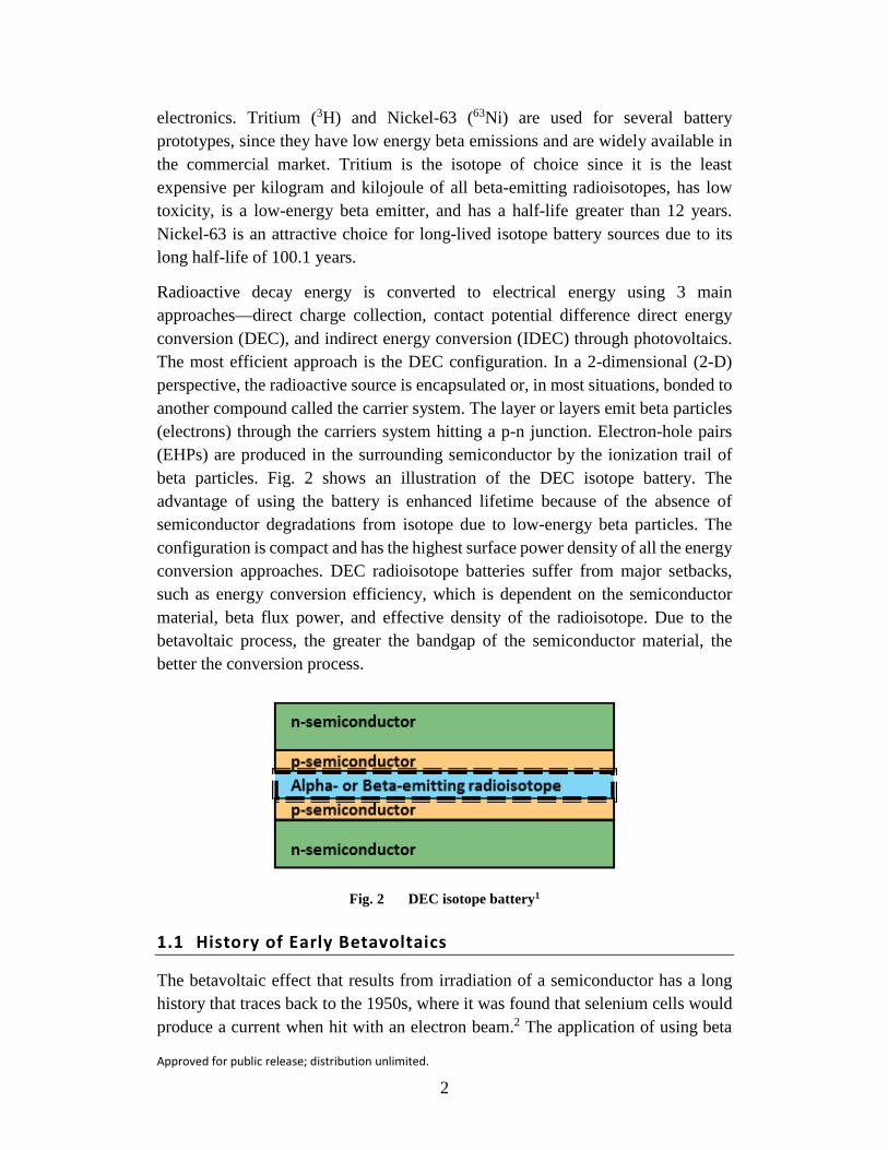
Radioactive decay energy is converted to electrical energy using 3 main approaches—direct charge collection, contact potential difference direct energy conversion (DEC), and indirect energy conversion (IDEC) through photovoltaics. The most efficient approach is the DEC configuration. In a 2-dimensional (2-D) perspective, the radioactive source is encapsulated or, in most situations, bonded to another compound called the carrier system. The layer or layers emit beta particles (electrons) through the carriers system hitting a p-n junction. Electron-hole pairs (EHPs) are produced in the surrounding semiconductor by the ionization trail of beta particles. Fig. 2 shows an illustration of the DEC isotope battery. The advantage of using the battery is enhanced lifetime because of the absence of semiconductor degradations from isotope due to low-energy beta particles. The configuration is compact and has the highest surface power density of all the energy conversion approaches. DEC radioisotope batteries suffer from major setbacks, such as energy conversion efficiency, which is dependent on the semiconductor material, beta flux power, and effective density of the radioisotope. Due to the betavoltaic process, the greater the bandgap of the semiconductor material, the better the conversion process.
Fig. 2 DEC isotope battery1
1.1 History of Early Betavoltaics
The betavoltaic effect that results from irradiation of a semiconductor has a long history that traces back to the 1950s, where it was found that selenium cells would produce a current when hit with an electron beam.2 The application of using beta

Approved for public release; distribution unlimited.
3
decay from radioactive isotopes such as strontium (Sr)90 was soon to follow that discovery.3 Selenium, germanium, and silicon (Si) solar cells were the first devices to be tested under the betavoltaic effect.2,4–8 Further research into Si cells was done to confirm the potential of betavoltaic cells.8–10 This resulted in the first commercially available betavoltaic battery, which was used to power pacemakers.11 However, due to the limits of Si in betavoltaic batteries, higher-energy isotopes were used. These high-energy isotopes would deteriorate Si cells. Using a semiconductor material with higher band-gap would give higher efficiency as well as being more radiation-hardy. The upper limit of betavoltaic conversion efficiency is completely dependent on the relationship of bandgap energy to the energy required to make an EHP within the device. Due to gallium nitride (GaN) and silicon carbide (SiC) having a large bandgap compared to other materials, the limit of their EHP generation efficiency is 34% and 33.8%, respectively. This efficiency is for ideal devices, and does not take into account the difference from intrinsic carrier concentration and density. This led to the research of SiC and GaN betavoltaic capability.
1.2 History of Silicon Carbide and Gallium Nitride Betavoltaics
Wide bandgap materials, such as SiC and GaN, were known to have a higher efficiency limit than Si and gallium phosphide (GaP) betavoltaics. An additional advantage of the wide bandgap of SiC and GaN is the increased power generation capability of the betavoltaic device, which is achieved through an increase of the open circuit voltage. The high on-state voltage matches with electrical circuit voltage requirements, leading to smaller DC-to-DC converter conversion ratios, thereby increasing conversion efficiency. The low on-state current also has a benefit of reducing the resistive losses that can occur. However, due to the lower current generation, losses due to shunt resistance are non-negligible. Device fabrication and packaging with strict quality requirements will improve the ability of the betavoltaic to produce energy above the shunt resistance. The fabrication of SiC and GaN semiconductors has been plagued by the presence of defects within the semiconductor material. The lack of high-quality semiconductor material prevented SiC and GaN in betavoltaic applications.
SiC betavoltaics were the first wide bandgap semiconductors to be commercially available as betavoltaic batteries12-13 because of the development of mass-production semiconductor processing methods of 4H-SiC. The ease of fabrication of thicker epitaxial layers make SiC a prime material for the use of betavoltaic cells. SiC is an attractive material due to its indirect bandgap, which can lead to better recombination time within the semiconductor. This can increase the diffusion collection of the semiconductor material. However, the research into the use of SiC

Approved for public release; distribution unlimited.
4
as a betavoltaic has yielded problems for increasing efficiency past 6% when used with beta isotopes such as 63Ni.14–16
GaN semiconductor devices offer the ability to increase the capability of betavoltaic direct energy converters due to GaN’s higher bandgap energy,16 radiation hardness,17 and intrinsic carrier concentration.15 Using Klein’s equation, the upper limit for GaN betavoltaic conversion at room temperature is 34%.18 GaN has a radiation threshold energy of 440 keV for electron irradiation, which is much higher than the spectrums of 63Ni and 3H.17 GaN lower intrinsic carrier concentration means there is less space-charge current within the device, allowing for a higher generation current when acting as a betavoltaic. GaN material fabrication processes are under research to improve the quality of GaN. GaN devices with high-quality material offer a direct improvement over SiC devices.
2. Software Tool Background
2.1 Silvaco ATLAS Background
Simulation of the semiconductor operation is done through Silvaco ATLAS, a physics-based technology computer-aided design (TCAD) device simulation software package. ATLAS simulates the electrical, optical, and thermal behavior of semiconductors through the use of finite element analysis.19 All device characteristics are derived from the basic equations. These equations are coupled partial differential equations, Poisson’s equation, the continuity equation, and the constitutive equation. Poisson’s equation connects the local charge densities and electrostatic potential together, while the continuity and constitutive equations describe the charge carrier densities, both electrons and holes, as charge carrier transport, generation, and recombination processes.
Silvaco ATLAS can simulate a device using various different types of physics models. These physics models add additional variables to the numerical calculations to derive the potential and current density. The lifetime in a semiconductor is composed of many different recombination parameters. The ability to add or remove different recombination models allows the investigation of how much that recombination model affects the performance of the device (e.g., removing or adding the radiative recombination model). This process is used throughout the report to see which physics processes optimized the performance of the device. An example of Silvaco ATLAS code is given in Appendix A.

Approved for public release; distribution unlimited.
5
2.2 MCNPX Background
MCNPX is a general-purpose Monte Carlo code that can be used to model neutron, photon, and electron (or coupled) transport.7,20 The transport code can track 32 types of particles. The extensive set of libraries contained within the code includes cross-sectional data and is able to simulate the transportation of these particles with energy from 1 keV to 100 MeV in materials. The MCNPX code-sets are used for design of spallation targets, design and development of radiography and imaging technologies, nuclear materials detection, accelerator shielding, and dose/energy deposition in materials for medical therapies.
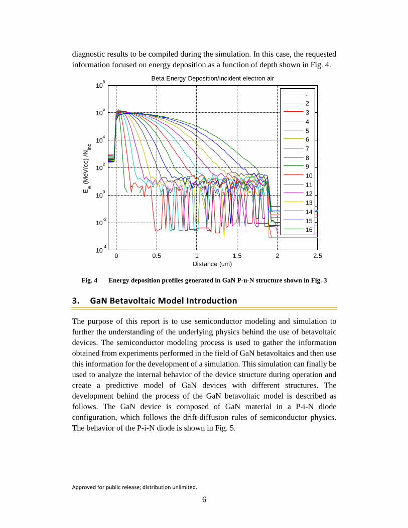
An electron beam with energies varied from 2 to 16 keV irradiated a GaN device shown in Fig. 3. The energy deposited in the device was calculated as a function of distance into the GaN device. The energy deposition profile calculated by MCNPX modeling is the basis for EHP profile deduced from the Klein equation.18 The EHP profiles are the basis for initial conditions in the Silvaco simulations described in this report. These energy deposition profiles in the GaN device for each of the applied electron beam energies are shown in Fig. 4. Each profile was fit to a polynomial as input to the electron-transport Silvaco simulations.
Fig. 3 A) Doping profile diagram and B) SEM image of GaN device evaluated composed of p-type (80 nm thick), undoped region (1 um thick), and n-type region (2 um thick)
The first sections of the MCNPX input deck (shown in Appendix B) describe the material elemental composition (GaN), density (6.15 g/cm3), and geometry. The middle sections describe the stimulus applied, which is a monenergistic 1 µm radius electron beam of 3 keV. The final section of the MCNPX input deck identifies
80nm pGan 4E17 cm-3
1um uGan 1E16 cm-3
2um nGan 3E18 cm-3
(A) (B)
Approved for public release; distribution unlimited.
6
diagnostic results to be compiled during the simulation. In this case, the requested information focused on energy deposition as a function of depth shown in Fig. 4.
Fig. 4 Energy deposition profiles generated in GaN P-u-N structure shown in Fig. 3
3. GaN Betavoltaic Model Introduction
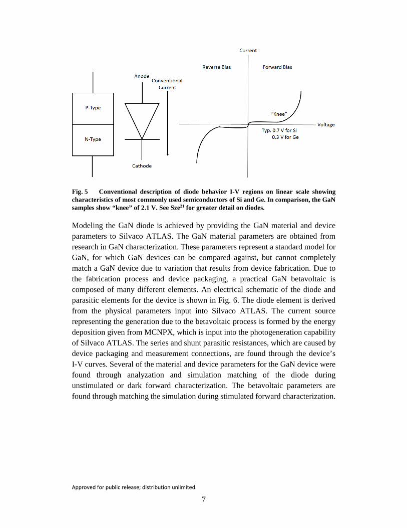
The purpose of this report is to use semiconductor modeling and simulation to further the understanding of the underlying physics behind the use of betavoltaic devices. The semiconductor modeling process is used to gather the information obtained from experiments performed in the field of GaN betavoltaics and then use this information for the development of a simulation. This simulation can finally be used to analyze the internal behavior of the device structure during operation and create a predictive model of GaN devices with different structures. The development behind the process of the GaN betavoltaic model is described as follows. The GaN device is composed of GaN material in a P-i-N diode configuration, which follows the drift-diffusion rules of semiconductor physics. The behavior of the P-i-N diode is shown in Fig. 5.
0 0.5 1 1.5 2 2.510
-4
10-2
100
102
104
106
108
Distance (um)
Ee (M
eV/c
c) /N
inc
Beta Energy Deposition/incident electron air
-2345678910111213141516
Approved for public release; distribution unlimited.
7
Fig. 5 Conventional description of diode behavior I-V regions on linear scale showing characteristics of most commonly used semiconductors of Si and Ge. In comparison, the GaN samples show “knee” of 2.1 V. See Sze21 for greater detail on diodes.
Modeling the GaN diode is achieved by providing the GaN material and device parameters to Silvaco ATLAS. The GaN material parameters are obtained from research in GaN characterization. These parameters represent a standard model for GaN, for which GaN devices can be compared against, but cannot completely match a GaN device due to variation that results from device fabrication. Due to the fabrication process and device packaging, a practical GaN betavoltaic is composed of many different elements. An electrical schematic of the diode and parasitic elements for the device is shown in Fig. 6. The diode element is derived from the physical parameters input into Silvaco ATLAS. The current source representing the generation due to the betavoltaic process is formed by the energy deposition given from MCNPX, which is input into the photogeneration capability of Silvaco ATLAS. The series and shunt parasitic resistances, which are caused by device packaging and measurement connections, are found through the device’s I-V curves. Several of the material and device parameters for the GaN device were found through analyzation and simulation matching of the diode during unstimulated or dark forward characterization. The betavoltaic parameters are found through matching the simulation during stimulated forward characterization.

Approved for public release; distribution unlimited.
8
Fig. 6 An equivalent circuit schematic of a practical p-n junction diode for betavoltaic operation. The diode element is controlled by the physical parameters of the GaN device, while the parasitic resistances were added by the device manufacturing and packaging processes. The current source describes the betavoltaic generation.
The diode model is dependent upon parameters that are specific to GaN material (e.g., mobility and intrinsic carrier concentration) and parameters that are specific to the device (e.g., doping concentrations and device dimensions). Silvaco ATLAS has default GaN material parameters that are included as default values for GaN. For example, the electron band structure of GaN from the default parameter list in Silvaco ATLAS is based upon prior research aggregated by Silvaco. The default parameter list covers properties of GaN material such as electron effective mass, hole effective mass, valence band reference, direct band gap at 300 K, spin-orbit split energy, crystal-field split energy, lattice constant, elastic constants, hydrostatic deformation potential, and shear deformation.22 These values are used for Fermi-Dirac statistics calculation to determine the effective conduction band and valence band density of states. However, the list of GaN parameters is not as extensive as Si, so missing parameters had to be found either through literature research or parametric sweeps. A list of the material and device properties of the GaN device can be found in Appendix C.
Even though GaN is not a completely understood material, the direct wide bandgap and electrical properties make it a good power semiconductor and betavoltaic converter. GaN has higher charge carrier mobility, breakdown field, and intrinsic carrier concentration than SiC. A comparison of semiconductor materials is shown in Table 1.

Approved for public release; distribution unlimited.
9
Table 1. Various semiconductors with their corresponding electrical and physical parameters. The parentheses values indicate Silvaco ATLAS default parameters for the material. The values in [] are from reference [23]. The remaining values are from reference [24].
Parameters Silicon (Si)
Gallium Arsenide (GaAs)
Silicon Carbide (4H-SiC)
Gallium Nitride (GaN)
Diamond (C)
Bandgap, Eg (Ev) 1.12(1.08) Indirect
1.43(1.42) Direct
3.26(3.23) Indirect
3.45(3.43) Direct
5.45 Indirect
Dielectric Constant, εr 11.9 (11.8)
13.1 (13.2)
10.1 (9.7)
9 (8.9)
5.5 [5.7]
Electric Breakdown Field, Ec (MV cm–1)
0.3 [0.23] 0.4 2.2
[2.2] 2
[3.3] 10
[5.6] Electron Mobility, μn (cm2 V–1s–1) 1,500 8,500 1,000 1,250 2,200
Hole Mobility, µp (cm2 V–1s–1) 600 400 115 850 850
Thermal Conductivity, Lambda (W cm–1 K–1) 1.5 0.46 4.9 1.3 22
Saturated Electron Velocity (x 107 cm–3 s–1)
1 (1.03)
1 (0.77)
2 (2.2)
2.2 (1.9)
2.7 (2)
Saturated Hole Velocity (1.03) (0.77) (1) (1) (0.1) Intrinsic Carrier Concentration (300 K)
[1.4e10] (1.45e10) (2.67e6) (1.73e-8) [1.9e-10]
(1.06e-10) [1e-22]
(1.58e-27) Electron Diffusion Coefficient25 36 200 22 25 57
Hole Diffusion Coefficient25 12 10 3 9 46
3.1 GaN Material Parameters
Carrier transport within the semiconductor is controlled by drift and diffusion. These equations are affected by the recombination that occurs within the device, mainly Shockley-Read-Hall (SRH) recombination. Recombination controls the carrier lifetime within the device. The carrier lifetime is a measure of how long a charge carrier lasts in the semiconductor before losing its charge and recombining. The minority carrier lifetime within the GaN device was found by using a parameter sweep described in Section 3.1.3. The Auger recombination for GaN has a negligible effect on current flow in the area where the GaN device was operating,26 and was not included into the simulation.
The physical parameters and carrier transport of semiconductor material are affected by radiation in numerous ways. The effects of ionizing radiation can cause EHPs to form within the device, as well as the creation of defects that change the doping level of the semiconductor material. Tunneling, recombination, and trapping can cause a reduction of generated current, which would happen in a practical device. Different effects that can be caused by radiation are shown in Fig. 7.27 The recombination and trapping effects are included into the model

Approved for public release; distribution unlimited.
10
through the effective carrier lifetime of the semiconductor device. The trap-assisted tunneling effect is also included into the model. The trap-assisted tunneling is where the trap acts as an intermediate state of the charge carrier as it moves into another band. It has been shown that it creates a significant contribution to current at the very low current density levels in LEDs.28 It is described further in Section 3.1.5. Shown in Fig. 8 is the betavoltaic process of EHP generation through a high-energy beta particle. The creation of phonons within the semiconductor is shown. This is covered by Klein’s equation (Section 4).
Fig. 7 Interactions of ionizing radiation with semiconductors, of which the generation of EHP is most significant effect in betavoltaics. Please see reference27 for greater detail.
Fig. 8 In this visualization of the creation of EHPs and phonons, a high-energy beta particle creates an EHP for every 10 eV in GaN. Se reference29 for greater detail.
3.1.1 Charge Carrier Mobility
Charge carrier mobility represents how quickly an electron can move through semiconductor material when an electric field is applied. This controls the drift velocity of the carriers within the material, which controls the on-state resistance of the material. Carrier mobility of a semiconductor is generally dependent on

Approved for public release; distribution unlimited.
11
temperature and doping concentration. Carrier mobility decreases as more dopants are introduced into the material, as the Coulombic forces introduced by these dopants can scatter the carriers moving through the material. Temperature can also introduce scattering due to lattice vibrations, called phonons, pushing carriers away. For the simulation model, the temperature was considered to be constant at 300 K, so the mobility model was only dependent on dopant concentration.
The charge carrier mobility within GaN is modeled using the Farahmand Modified Caughey Thomas (FMCT) model. This is a Monte Carlo fitting of the Caughey Thomas model to represent the electron mobility within the semiconductor and is based upon the work done by Farahmand30. The model parameters were found by doing a parameter sweep and using the parameters that best fit the experimental data. The FMCT model is an impurity concentration and temperature-dependent mobility model, and the concentration dependence of the electron mobility is shown in Fig. 9.
Fig. 9 Default electron mobility in GaN material with respect to total impurity doping concentration in Silvaco ATLAS using the FMCT model
3.1.2 GaN Deep-Level Traps
Semiconductor devices have defects within their material caused from various sources. These sources can occur from the fabrication process or from radiation-induced damage. Defects are imperfections within the crystalline structure. These imperfections can be characterized as point defects, which are missing atoms or extra atoms to the unit cell, or stacking and threading dislocations, which are where the layers of the crystalline structure do not have a perfect bond. These defects create additional energy states within the device called traps. Trap energy states are energy levels within the band-gap of the device. Deep level traps, which are traps
0
200
400
600
800
1,000
1,200
1,400
1,600
1.0E+13 1.0E+14 1.0E+15 1.0E+16 1.0E+17 1.0E+18 1.0E+19 1.0E+20
Mob
ility
(cm
2 V-1
s-1)
Material Total Dopant Concentration (cm-3)
Electron Mobility in GaN

Approved for public release; distribution unlimited.
12
of sufficient energy difference from the conduction or valence band that they do not thermally activate within the material, create a recombination mechanism of charge carriers within the device. This mechanism is called SRH recombination. SRH recombination is the primary method of recombination within indirect bandgap materials such as Si or SiC and is a dominant recombination mechanism within direct bandgap devices depending on the material quality and operation area. Due to the current technology for GaN device fabrication, GaN trap states are caused by various point defects and threading dislocations. The amount of defects is controlled by the type of substrate material, as well as by the device fabrication process. Current substrates used for GaN fabrication have a difference in lattice size and, therefore, can create more defects the larger the lattice mismatch. The GaN device used for the betavoltaic experiments was created using a sapphire (Al2O3) substrate. The trap levels used for simulation are generalized on traps from research on GaN trap levels.31–33 The trap levels used for the experiment are shown in Table 2.
Table 2 Commonly used traps for GaN, and their concentrations31–33
Trap Designation Trap Type
Energy from Valence band
(eV)
Density of States Concentration
(cm–3)
Capture Cross Section (cm2)
H2 Donor 0.55 2.4 × 10¹⁴ 2.7 × 10⁻¹² H3 Donor 0.65 2.1 × 10¹⁴ 1.7 × 10⁻¹⁴ H4 Donor 0.85 3.4 × 10¹⁴ 1.8 × 10⁻¹³ H5 Donor 1.20 2.9 × 10¹⁵ 4.7 × 10⁻¹⁴ E1 Acceptor 0.17 1.0 × 10¹⁴ 2.3 × 10⁻¹⁷ E2 Acceptor 0.52 9.0 × 10¹⁴ 3.3 × 10⁻¹⁶ E3 Acceptor 0.53 5.8 × 10¹⁴ 3.3 × 10⁻¹⁷ E4 Acceptor 0.94 5.8 × 10¹⁵ 1.0 × 10⁻¹⁶
The density of these traps describes how much they occur throughout the device. A parameter sweep to show the effect of trap density upon on the device is shown in Fig. 10. This parameter sweep is done using a stimulated I-V curve to show how the performance of the betavoltaic degrades. The parameter sweep shows that the traps can act as dopants in the material, as after the trap level overcomes the intrinsic region doping, the p-n junction switches to between the intrinsic and N+ region. This is out of the electron beam range for 3 keV, so that no carriers are collected. This results in a regular p-n junction that follows Shockley’s diode equation, which can be seen in the I-V curves.

Approved for public release; distribution unlimited.
13
Fig. 10 I-V curve comparison using the traps from Table 2 with a parameter sweep of the density of the traps. The traps were swept from 1013 to 1018 cm–3. Below 1015 cm–3, the different densities had minimal change on the stimulated I-V curve. Occurring at 1015 cm–3and above, the trap density of states overcame the background doping concentration of the unintentionally doped layer, which changed the p-n junction to the interface between the N+ and unintentionally doped regions.
3.1.3 Minority Carrier Lifetime
Minority carrier lifetime is composed of 3 types of recombination: SRH, Auger, and Radiative.21 The relationship between minority carrier lifetime and each individual recombination is
1𝜏𝜏𝑏𝑏𝑏𝑏𝑏𝑏𝑏𝑏
=1
𝜏𝜏𝑆𝑆𝑆𝑆𝑆𝑆+
1𝜏𝜏𝐴𝐴𝑏𝑏𝐴𝐴𝐴𝐴𝐴𝐴
+1
𝜏𝜏𝑆𝑆𝑅𝑅𝑅𝑅𝑅𝑅𝑅𝑅𝑅𝑅𝑅𝑅𝑅𝑅𝐴𝐴, (1)
or rearranged is 1
1𝜏𝜏𝑆𝑆𝑆𝑆𝑆𝑆
+ 1𝜏𝜏𝐴𝐴𝑏𝑏𝐴𝐴𝐴𝐴𝐴𝐴
+ 1𝜏𝜏𝑆𝑆𝑅𝑅𝑅𝑅𝑅𝑅𝑅𝑅𝑅𝑅𝑅𝑅𝑅𝑅𝐴𝐴
= 𝜏𝜏𝑏𝑏𝑏𝑏𝑏𝑏𝑏𝑏, (2)
where the smallest time to recombine results in the dominating factor for the minority carrier lifetime. Under most circumstances with most indirect materials, this is generally SRH recombination. Auger recombination starts to have a noticeable effect at high-current densities and is not taken into account in the simulation due to the very low current densities of the device. Radiative recombination is also activated within the device due to the direct bandgap of GaN.
-5E-09
0E+00
5E-09
1E-08
2E-08
2E-08
0.0 0.1 0.2 0.3 0.4 0.5 0.6 0.7 0.8 0.9 1.0 1.1 1.2 1.3 1.4 1.5 1.6 1.7 1.8 1.9 2.0 2.1 2.2 2.3 2.4 2.5
Curr
ent (
A)
Voltage (V)
Trap Density Parameter Sweep3 keV Electron Beam Stimulated
Trap Density = 10^13 Trap Density = 10^14Trap Density = 10^15 Trap Density = 10^16Trap Density = 10^17 Trap Density = 10^18

Approved for public release; distribution unlimited.
14
3.1.3.1 Shockley-Read-Hall Lifetime Sweep
The device minority carrier lifetime is affected by various defects within the device, which reduces the “knee” point of the device. The lower the minority carrier lifetime value, the more the knee voltage of the device shifted to a lower voltage value. The minority carrier lifetime was swept logarithmically from 1 fs to 1 s to match the experimental results of the GaN device. The results of this parametric sweep are shown in Fig. 11. As shown in the graph, lifetime values greater than 10 ps result in knee voltages that are greater than thLe experimental results gathered and were eliminated as possibilities.
Shown in Fig. 11 are the results from the minority carrier sweep with respect to the measured results. The lifetimes that gave negligible results were removed. As can be seen from Fig. 11, the closest lifetime value to the measured results is 1 ps. However, the slope of the simulated result does not match the measured result. This is due to more missing parasitic elements, such as the equivalent series resistance of the device.
Fig. 11 Minority carrier lifetime variation from 10–15 to 1 s was performed to match to device data. Best fit found at 10–12 s.
3.1.3.2 Radiative Recombination Parameter Sweep
Radiative recombination is where an electron in the conduction band recombines with a hole in the valence band, and the excess energy is given off as a photon. In the case of GaN, this photon would be in the ultraviolet (UV) spectrum. Eq. 3 represents the calculation of radiative recombination within the simulation. Emission factor is the faction of energy that propagates in a specified direction of interest that is used with laser simulations, and was not used. The Optical Capture
0E+00
5E-07
1E-06
2E-06
2E-06
3E-06
2.20 2.22 2.24 2.26 2.28 2.30 2.32 2.34 2.36 2.38 2.40 2.42 2.44
Curr
ent (
A)
Voltage (V)
Minority Carrier Lifetime IV ComparisonMeasured vs Simulated
Measured Dark Current1 fs10 fs100 fs1 ps10 ps

Approved for public release; distribution unlimited.
15
Rate (COPT) controls the radiative recombination, which is a material parameter. The default value in Silvaco ATLAS was 1e–8 cm3 s–1, and was swept from 10–10 to 10–6 cm3 s–1. The result of this sweep is shown in Fig. 12.
𝐸𝐸𝐸𝐸𝐸𝐸𝐸𝐸𝐸𝐸𝐸𝐸𝐸𝐸𝑛𝑛𝐹𝐹𝑅𝑅𝐹𝐹𝑅𝑅𝐹𝐹𝐴𝐴 ∗ 𝐶𝐶𝐶𝐶𝐶𝐶𝐶𝐶 ∗ (𝑛𝑛 ∗ 𝑝𝑝 − 𝑛𝑛𝑅𝑅2) = 𝑅𝑅𝑅𝑅𝑅𝑅𝐸𝐸𝑅𝑅𝑅𝑅𝐸𝐸𝑅𝑅𝑅𝑅 𝑅𝑅𝑅𝑅𝑅𝑅𝐸𝐸𝐸𝐸𝑅𝑅𝐸𝐸𝑛𝑛𝑅𝑅𝑅𝑅𝐸𝐸𝐸𝐸𝑛𝑛. (3)
Fig. 12 Radiative recombination parameter variation shows insignificant change in generation current for 3-keV electron beam. The higher COPT resulted in a lower generation current.
As can be seen from Fig. 12, the change of radiative recombination over 4 orders of magnitude resulted in minimal effect. This follows that the GaN device was dominated by SRH recombination. The GaN simulation was kept at the default value of 1e–8 cm3 s–1 for COPT for the rest of the simulation.
3.1.4 Surface Recombination
Surface recombination is a mechanism that describes how well a betavoltaic or photovoltaic can collect diffusion current. At the surface of semiconductors, dangling bonds are left due to the end of the crystalline structure. These dangling bonds create active states that charge carriers can recombine with, which further reduces the carrier lifetime in a device. Surface recombination plays a major role in diffusion collection, depending on how likely a charge carrier is to recombine at the surface. Diffusion current is the random movement of EHPs in a semiconductor to restore equilibrium throughout the device. As charge carriers on the surface recombine, charge carriers in the bulk will diffuse towards the surface rather than
-3.5E-09
-3.0E-09
-2.5E-09
-2.0E-09
-1.5E-09
-1.0E-09
-5.0E-10
0.0E+00
5.0E-10
1.0E-09
0.0 0.2 0.4 0.6 0.8 1.0 1.2 1.4 1.6 1.8 2.0
Curr
ent (
A)
Voltage (V)
Radiative Recombination Sweep IV Curve3 keV Electron Beam Stimulated
Copt = 1e-6Copt = 1e-10

Approved for public release; distribution unlimited.
16
the depletion region. For normal solar cells, diffusion current plays a large role in collecting EHPs.
For the measured GaN device, the diffusion length of the device is insignificant due to the minority carrier lifetime. Shown in Eq. 4, the diffusion length within the device is 50 nm. This value was calculated from the minority carrier lifetime, 1 ps, and the GaN electron diffusion coefficient, 25 cm2 s–1.25 This means that diffusion collection is very small. This is corroborated with the activation of the surface recombination model in Silvaco ATLAS. The I-V curve comparison is shown in Fig. 13.
√𝜏𝜏 ∗ 𝐷𝐷 = 1 𝑝𝑝𝐸𝐸 ∗ 25
𝑅𝑅𝐸𝐸2
𝐸𝐸= 50 𝑛𝑛𝐸𝐸. (4)
Fig. 13 I-V curve comparison of surface recombination on electron beam stimulated I-V curves. The difference between the I-V curves is minimal, which shows that the effect of surface recombination on the collection of EHPs due to diffusion is minimal. This determined that EHP collection was dominated by the depletion region collection.
3.1.5 Trap-Assisted Tunneling
Trap-assisted tunneling is a phenomenon where a charge carrier can transfer through a potential barrier through the usage of a trap. This can lead to increased current at very low voltage levels. This generally occurs with heterojunction devices such as LEDs. The GaN betavoltaic device power level is operated at a range where trap-assisted tunneling can make a significant difference in the behavior of the device. A visual representation of an electron recombining with a hole in the valence band is shown in Fig. 14.
-3.5E-09
-3.0E-09
-2.5E-09
-2.0E-09
-1.5E-09
-1.0E-09
-5.0E-10
0.0E+00
0.00
0.10
0.20
0.30
0.40
0.50
0.60
0.70
0.80
0.90
1.00
1.10
1.20
1.30
1.40
1.50
1.60
1.70
1.80
1.90
2.00
2.10
Curr
ent (
A)
Voltage (V)
3 keV Electron Beam IV CurveSurface Recombination Effect
No Surface Recombination
Activated Surface Recombination

Approved for public release; distribution unlimited.
17
Fig. 14 Demonstration of trap-assisted tunneling mechanism. An electron can transfer into the valence band, or vice versa, through use of a trap, thereby “tunneling” through the potential barrier. This parameter was varied [0.05mo, 0.8 mo], well beyond the 0.25 level of Si.
A parametric sweep over different effective masses for tunneling was performed to characterize the effect of trap-assisted tunneling on the betavoltaic response. This sweep was performed from 0.05 times the mass of an electron at rest to 0.80 times the mass of an electron at rest. The sweep was performed while the device was stimulated. The resulting I-V curves are shown in Fig. 15 characterizing the change due to tunneling.

Approved for public release; distribution unlimited.
18
Fig. 15 I-V curves showing the effect of sweeping the effect mass of the tunnel state. This parameter was varied [0.05mo, 0.8 mo], well beyond the 0.25 level of Si. The smaller the effective mass, the more current would tunnel through the potential barrier, reducing the effective generation current. The GaN simulation was kept at 0.25mo.
3.2 GaN Device Parameters
3.2.1 GaN Device Doping Profile
The simulated GaN device structure was to represent the experimental device as closely as possible. The GaN DEC device was a P-u-N diode. The P-u-N device doping levels were 4e17 cm–3 for the P-region, 1e16 cm–3 for the unintentionally doped region, and 1e18 cm–3 for the N+ region. The N- region in GaN devices is also called the unintentionally doped region, due to the high background concentration of oxygen and carbon impurities within the growth process of MOCVD.34 The doping profile of the device was uniform for the N+ and intrinsic regions. The P-region used a Gaussian implantation for the doping of the region. The Gaussian distribution was chosen because it approximately matches the doping profile given by MOCVD.35 As-implanted and after-annealing GaN material doped with Mg+ dopants are shown to obtain a maximum at some depth in the device and fall off rapidly.35 This is compared to the doping profile used in the Silvaco ATLAS model in Fig. 16. The figure shows that at the p-n junction results in a “zero” net dopant concentration within Silvaco ATLAS.
-5E-09
-4E-09
-3E-09
-2E-09
-1E-09
0E+00
1E-09
2E-09
0.0 0.1 0.2 0.3 0.4 0.5 0.6 0.7 0.8 0.9 1.0 1.1 1.2 1.3 1.4 1.5 1.6 1.7 1.8 1.9 2.0 2.1
Curr
ent (
A)
Voltage (V)
Trap-Assisted Tunneling Mass Parameter Sweep3 keV Electron Beam Stimulated
Tunnel Mass - 0.05Tunnel Mass - 0.10Tunnel Mass - 0.20Tunnel Mass - 0.25Tunnel Mass - 0.30Tunnel Mass - 0.40Tunnel Mass - 0.60Tunnel Mass - 0.80

Approved for public release; distribution unlimited.
19
Fig. 16 Doping profile of GaN model used in Silvaco ATLAS based on typical results in devices described in literature
Using the device’s physical parameters, such as the doping profile and layer thickness, Silvaco ATLAS was used to calculate the built-in potential and zero-bias internal electric field. These images are shown in Fig. 17. Inputting the device doping profiles and thicknesses into Silvaco ATLAS allows the computation of the built-in potential of the device and the zero-bias electric field. The built-in potential shows how the energy bands of the semiconductor change with respect to the depth. This value cannot be measured in a real device. The internal electric field shows the depletion region within the device. This is an important parameter of betavoltaics, as the depletion region collects the EHPs within the device. The depletion region is approximately 500 nm in width, and is shown as the brightly colored areas centered around 80 nm.
1E+00
1E+02
1E+04
1E+06
1E+08
1E+10
1E+12
1E+14
1E+16
1E+18
0.00 0.03 0.05 0.08 0.15 0.27 0.40 0.52 0.65 0.77 0.90 1.02 1.09
Abso
lute
Dop
ing
(cm
-3)
Depth (Microns)
Doping Profile Of Modeled Device
Unintentionally doped region or intrinsic region
N+
N-
P+

Approved for public release; distribution unlimited.
20
Fig. 17 A) The built-in potential of the device. The variation of the potential in the semiconductor is due to band-bending due to the formation of junctions with different fermi levels. B) The zero-bias electric field of the device. The field variation is biggest at the p-n junction, with a small electric field built at the junction between the intrinsic and n+ regions.
3.2.2 Space Charge Generation Current
The matching process of simulation to the experimental device started with the dark I-V curve, which is the forward characteristic of the device when the device is not stimulated by an external beta source. The dark I-V curve is composed of different regions. These regions are each controlled by various physical parameters within the device. The space charge generation region is controlled by the diffusion of charge carriers within the device. This current, also called saturation current, can be calculated for an ideal diode using Equation 5.
𝐼𝐼𝑠𝑠 = 𝑞𝑞𝑞𝑞
𝐷𝐷𝑝𝑝𝜏𝜏𝑝𝑝
𝑛𝑛𝑅𝑅2
𝑁𝑁𝐷𝐷+
𝐷𝐷𝑛𝑛𝜏𝜏𝑛𝑛
𝑛𝑛𝑅𝑅2
𝑁𝑁𝐴𝐴. (5)
The parameters used in the equation are q for elementary charge; A for the cross-sectional area of the device; Dn and Dp for the diffusion constants in GaN of electrons and holes, respectively; τp and τn for the lifetime of the electrons and holes in GaN, respectively; ni for the intrinsic carrier concentration of GaN; ND for the donor doping concentration; and NA for the electron doping concentration. Thus, the space charge generation current is controlled by these physical parameters of the device. The space charge generation current was matched by using the proper dimensions and doping concentrations of the real device. However, due to the extremely low value of saturation current due to the intrinsic carrier concentration of GaN, the ideal saturation current is much lower than a practical device’s current at low voltages. This extra current is due to other physical parameters within the device, such as trap-assisted tunneling and shunt resistance.
(A)
(B)

Approved for public release; distribution unlimited.
21
3.2.3 Shunt Resistance Leakage Current
Leakage current dominated the low current density region of the device. Leakage current can occur due to factors, such as device threading or stacking defects, or conduction paths developed within the device package and device interface surfaces. The leakage current of the device is seen in the linear-scale I-V curve before the knee of the I-V curve. This region of the I-V curve was simulated using an equivalent shunt resistance added to the device. This shunt resistance value was found by taking the forward characteristics of the GaN device and performing a linear fit on the section of the curve before the knee of the I-V curve. The slope of this line was the equivalent conductance of the shunt resistance and is shown in Equation 6. The equivalent shunt resistance value was then calculated and input into the simulation in parallel with the simulated device. The shunt resistance value is shown in Equation 7. Shown in Fig. 18 is the dark I-V curve of the measured device and the linear fit obtained. At approximately 0.7–1.7 V, there is a linear dependence of the I-V curve that represents the equivalent shunt resistance.
𝐺𝐺 =1𝑅𝑅
=𝐼𝐼𝑉𝑉
= 3.65 × 10⁻¹⁰ , (6)
𝑅𝑅 =1𝐺𝐺
=𝑉𝑉𝐼𝐼
= 2.7 × 10⁹ Ω. (7)
3.2.4 Series Resistance
The series resistance of the simulation was set to the series resistance measured from a GaN device of the same wafer and device package as the measured device. The reference device was characterized to high current densities to reach the series region. Using a linear fit at the high-current densities of the I-V curve, the series resistance was found to be 3.72 Ω (ohm). The I-V curve and the linear fit of the series conductance is shown in Fig. 18. The series resistance region is shown in detail in Fig. 19. The series resistance was calculated using the same process in calculating the shunt resistance with Equations 6 and 7.

Approved for public release; distribution unlimited.
22
Fig. 18 Dark I-V curve for the measured device. The I-V curve shows the linear fit used to determine the equivalent dark current. This equivalent shunt resistance mainly effects the shaded area of the I-V curve. The equivalent shunt resistance was determined by taking the inverse slope of the linear fit.
Fig. 19 I-V curve for GaN device #17. The linear fit, represented by the dotted line, gives a series resistance of 3.72 Ω.
Typical diodes have series resistance in the mΩ range. The structure of this device was not necessarily meant to minimize series resistance. The resistance value includes all series elements from the diode to the parameter analyzer; the device metal contacts, the wire bonds, and the package leads, as well as the test leads to the device package, make up this value. This series resistance measurement has a
0.00E+00
1.00E-10
2.00E-10
3.00E-10
4.00E-10
5.00E-10
6.00E-10
7.00E-10
0 0.2 0.4 0.6 0.8 1 1.2 1.4 1.6
Curr
ent (
A)
Voltage (V)
GaN Measured Dark Current IV CurveShunt Resistance Linear Fit
GaN Dark CurrentLinear (GaN Dark Current)
0.20
0.21
0.22
0.23
0.24
0.25
0.26
0.27
0.28
0.29
0.30
4.86 4.90 4.93 4.95 4.99 5.01 5.05 5.07 5.09 5.12 5.14 5.17
Curr
ent (
A)
Voltage (V)
GaN Device #17 IV CurveSeries Measurement Derivation
Current (A) Linear (Current (A))

Approved for public release; distribution unlimited.
23
very small effect on the I-V curves of the simulation, due to the low current densities that the device operates in. The series resistance value is added to the model to make the model more accurate, allowing the slope of the knee region to be found by changing other parameters.
3.2.5 Measured and Simulated Dark Current I-V Curve Comparison
The various physics parameters controlling dark current described in the previous sections were used to create a simulated betavoltaic device. This device simulation is compared to the parameter analyzer results which is shown in Fig. 20. The comparison shows the simulation follows the trend of the actual device I-V curves.
The similarity between the simulation result and the real device I-V curve represents the similarity of the simulation parameters to the actual device. The doping profile can be assumed to be fairly close due to the on-state turn-on voltage of the device. The series resistance can be examined in the slope of the on-state I-V region. The space charge and shunt resistance match closely in the region before the knee voltage of the device. The disparity at the very low bias region shows that more physical parameters can be deduced.
Fig. 20 Dark Current I-V Comparison between the real device and the simulated device, with normalized root mean square error of 14.82%, from 0.5 to 2.4 V. This value was calculated using the data from the parameter analyzer without smoothing.
1.0E-18
1.0E-16
1.0E-14
1.0E-12
1.0E-10
1.0E-08
1.0E-06
1.0E-04
1.0E-02
1.0E+00
0.0 0.2 0.4 0.6 0.8 1.0 1.2 1.4 1.6 1.8 2.0 2.2 2.4
Curr
ent (
A)
Voltage (V)
Dark Current IV CurvesReal vs. Simulated
Real DeviceSimulated Device

Approved for public release; distribution unlimited.
24
4. Stimulated Forward Characteristics
4.1 Stimulated Modeling Introduction
The model of the GaN device needed to match the measured device when stimulated by an low-energy electron beam. This stimulation represents the betavoltaic current source in the equivalent schematic shown in Fig. 5. A betavoltaic operates in a circuit by the device collecting EHPs that are generated due to incoming radiation. Electrons that are collected are then passed through the circuit. The EHPs that are generated in a semiconductor were generated through 2 profiles, a linear approximation and results generated in MCNPX. These EHP profiles allow for the simulation of the electron beam-induced current (EBIC). The maximum power points (MPPs) are gathered from the stimulated I-V curves to show how the electron beam range affects the generation of the device and what factors control betavoltaic energy production.
4.2 Electron Beam Experiment Background
The measured GaN device was exposed to electron beams in a process similar to EBIC characterization. The device was hit by electron beams with different electron energies from 2–16 keV, and the resulting I-V characteristics were taken on a parameter analyzer. The current distribution of the electron beam was measured and a profile for the beam distribution with respect to various beam energies was made. The beam current profile of the device was found to have a Gaussian distribution for each beam energy, with an full-width half-maximum that decreased with increasing energy. The variation of the electron beam profile changes the beam current incident to the GaN device tested. More details on this experiment can be found in Litz36. The incident beam current and beta radiation energy from these experiments were used to generate the MCNPX EHP profiles within the device.
4.3 GaN Device Electron-Hole Pair Calculation and Simulation
The simulation of the stimulated response of the GaN device was accomplished through using EHP generation profiles within the semiconductor. The EHP profiles were approximated by a linearly decreasing energy deposition profile, and then were generated using MCNPX results. The energy deposition within the semiconductor directly represents the EHP generation within the device. The energy deposition is converted into EHP using the Klein relationship. Using Klein’s equation, the value required to generate an EHP in GaN was found to be 10 eV. This is shown in Equation 8.
Approved for public release; distribution unlimited.
25
𝜖𝜖 = 145𝐸𝐸𝐴𝐴 + 𝑟𝑟(ℎ𝜔𝜔𝑆𝑆) ≈ 10 𝑅𝑅𝑉𝑉. (8)
Part of our verification approach included a linear EHP profile as an initial condition. While understanding that this was not accurate, it allowed us to understand how important the MCNPX calculated energy deposition distribution is to resulting I-V curve solutions. The more accurate EHP profile with a greater number of EHP in the depletion region shows the value of the distribution of the energy deposition profiles in the charge carrier transport modelling of Silvaco ATLAS.
4.3.1 Linear and MCNPX Calculated Energy Deposition
Using Klein’s relationship, the 10 eV value means that a 5-keV electron would ideally generate 500 EHPs within the device. In the linearly decreasing profile, a 5-keV electron energy deposition beam would be scaled so that the total EHPs generated within the volume of the device would equal 500. Each discrete point was then divided by the representative volume of that point to obtain the EHPs generated per cubic centimeter. Finally, the curve was scaled by the beam current, which is the number of electrons the device was exposed to per second, obtained from the electron beam experiments on the measured device. The stimulated device I-V curves using a linear energy deposition profile allowed for the evaluation of default parameters for GaN defaults provided by Silvaco ATLAS that affect EHP generation. All I-V curve results shown for a stimulated I-V curve in this report used a MCNPX result, except for Fig. 22.
After verifying the capability of Silvaco ATLAS to model the betavoltaic experiment with a linear profile, the energy deposition profile for the various electron energies (2–16 keV) in the GaN material was modeled using MCNPX. Detail on the generation of these EHP profiles is described in Section 2.2. A comparison of the first-order guess of energy deposition (linear profile) compared to the Monte-Carlo calculated energy deposition from monenergistic electron beams is shown in Fig. 21. A comparison of how the shape of the EHP generation affects I-V curves is shown in Fig. 22. Fig. 22 shows the I-V curve results from each energy deposition profile (linear vs MCNPX) when the profiles are normalized to the same EHP generation within the total volume. This shows how, when the total EHP generation is contained within the depletion region, the device has greater short circuit current and generated power.

Approved for public release; distribution unlimited.
26
Fig. 21 Energy deposition profiles (linear and MCNPX) of 5-keV electron beam incident on GaN device. The EHP profiles represent the same amount of EHP generation throughout the GaN device and only differ in the shape of the EHP curve. This was used to verify that the EHP distribution within the semiconductor changes the resulting I-V curve.
Fig. 22 I-V curve comparison for a 5-keV electron beam incident on GaN device is shown for both linear and MCNPX numerically calculated energy deposition profile. The MCNPX profile results in a much greater generated current for the same total EHPs in the device. The ripples in the I-V curves are a result of early simulation input decks and have an absence of many parameters such as traps.
0.0E+00
2.0E+16
4.0E+16
6.0E+16
8.0E+16
1.0E+17
1.2E+17
1.4E+17
1.6E+17
00.
025
0.05
0.07
50.
10.
125
0.15
0.17
50.
20.
225
0.25
0.27
50.
30.
325
0.35
0.37
50.
40.
425
0.45
0.47
50.
5
EHPs
(cm
-3s-1
)
Depth (Microns)
EHP Profile Comparison5 keV Electron Beam Stimulus
Linear ProfileMCNPX Profile
0.0%
20.0%
40.0%
60.0%
80.0%
100.0%
0.02 0.22 0.42 0.62 0.82 1.02 1.22 1.42 1.62 1.82
Nor
mal
ized
Out
put C
urre
nt
Voltage (V)
Simulated IV Curves ComparisonLinear vs MCNPX Profile
MCNPX Profile
Linear Profile

Approved for public release; distribution unlimited.
27
4.3.2 Silvaco Electron-Hole Pair Calculation
The process for the betavoltaic interaction using Silvaco ATLAS is described in this section. Silvaco ATLAS is a numerical calculation of charge carrier densities and electrostatic potential, and is not a program that simulates the particle physics of high-energy beta particles striking GaN molecules. A beta particle that strikes an atom within the GaN device creates an EHP, which is very similar to how the photovoltaic operation of a solar cell works. Therefore, using the effects of the beta particle striking the device—e.g., the EHP generation due to the beta particle—we can create an EHP generation profile using the Silvaco ATLAS Luminous module, which is a description of how EHPs affect the basic equations. The EHP generation within the device was calculated from the energy deposition profiles detailed in Sections 2.2 and 4.3.
Silvaco ATLAS devices are created using meshes for finite element calculation. The correct implementation of EHP generation into the device requires knowledge of how Silvaco ATLAS compensates generation within the mesh. The mesh is a description of the areas within the device from which the basic equations are calculated. The mesh separates the device into many different triangles that are generated from the specified mesh points. Silvaco ATLAS EHP generation rate uses units of EHPs cm–3 s–1, which represents the EHPs generated within each triangle with respect to the particles per second hitting the device.
Using the mesh points within the device, the energy deposition curve for each keV was normalized into several different bins with respect to depth. Each mesh point in the y-axis, which is the depth of the device, is then represented by a bin. The summation of the bins in the y-axis must equal the ideal Klein ratio for an electron with a specified energy—e.g., for a 12-keV electron, there would be 1,200 EHPs generated in the 100- × 100-µm device. Due to the device simulation process the z-axis for the device is 1 µm, where Silvaco ATLAS then scales the results by 100 to represent the 100 × 100-µm device. Because of this scaling factor, the summation of the bins in the y-axis must equal the ideal Klein ration divided by 100—e.g., a 12-keV electron would generate 12 EHPs within the 3.08- × 100- × 1-µm volume. This slice represents the volume that ATLAS actually simulates for a 2-D simulation (Fig. 23). This gives the number of EHPs generated in the device due to 1 particle with respect to depth. To match the units given by Silvaco ATLAS, the mesh point values are scaled by 2 factors: the volume around each mesh point and the number of beta particles that can pass through a given triangle per second. The number of particles corresponds to the incident beam current hitting the device.

Approved for public release; distribution unlimited.
28
Fig. 23 Shown is the surface area of the top of the simulated device representing how Silvaco ATLAS simulates a device. A 1-µm “slice” in the Z-axis is simulated, which is then scaled by the Z-axis value to represent the total device.
The Luminous simulator within the Silvaco ATLAS software can have any arbitrary generation profile using a C programming language function. The function provides the position using the x, y, and z coordinates for each point in the mesh. Using this position, the function then retrieves an EHP generation rate, either from calculating the EHP generation at that depth using an EHP profile equation or by using a look-up table that contains a list of prior calculated EHPs for each mesh point. To ensure accuracy of the betavoltaic experiment within the simulation, the function needs to ensure that all points within the device are represented. Discontinuities can occur due to an absence of an EHP value or large mesh spacing. The EHP generation used polynomial equations in the betavoltaic simulations, which were approximations of the MCNPX results. The code to produce these simulations in Silvaco ATLAS is shown in Appendix D. A list of the polynomial equations and the C language function to calculate the EHP generation with respect to depth is shown in Appendix E.
A comparison of the Silvaco ATLAS generation profiles compared to the MCNPX generated result is shown in Fig. 24. The EHP generation profile was generated using a fourth-order polynomial equation, which provides a close match to the MCNPX result. The approximate zero-bias depletion region is shown in the figure to compare how the generation compares with the depletion region. The p-n junction is represented by a red line in the figure. The curves were normalized to make the comparison between the profiles.

Approved for public release; distribution unlimited.
29
Fig. 24 EHP Generation profiles for 12-keV electron beam stimulus from MCNPX result and Silvaco ATLAS simulation result. The simulation profile is a fourth-order approximation of the MCNPX result. The profiles show the maximum generation at 180 nm within GaN. This shows that the extra EHP generation past the depletion region is wasted. The P-N junction is indicated at the vertical red line.
The input beam currents for the stimulated experiments are shown in Table 3 and Fig. 25. Due to mismatch of the simulation to the model, the EHP generation profile was scaled to have the simulated device short circuit current match the measured device short circuit current. This scalar represents the input beam current exposed to the device. The resulting input currents are then compared against the calculated input beam currents. The simulation beam currents are much higher than the Gaussian calculated currents. This could be a result from differing EHP generation profiles, GaN material properties, or inaccurate device properties. This discrepancy is discussed in Section 5.
0
0.2
0.4
0.6
0.8
1
1.2
0 0.1 0.2 0.3 0.4 0.5 0.6 0.7 0.8 0.9 1
Nor
mal
ized
Uni
ts
Device Depth (Microns)
MCNPX Result vs Silvaco ATLAS EHP Profile
12 keV EHP Profile
Simulation EHP Profile
MCNPX EHP ProfileZero-Bias
Depletion Region

Approved for public release; distribution unlimited.
30
Table 3 Input beam currents for the various experimental runs are tabulated. The simulation result for current is larger than the Gaussian calculated beam currents in all cases, suggesting that the simulation EHP model does not include a complete physical description of the experiment.
Input electron energies
(keV)
Simulation input beam current
(A)
Gaussian beam calculated input
beam current (A)
3 4.80E-11 1.89E-13 5 1.32E-10 1.64E-12 7 1.36E-10 6.50E-12 10 2.03E-10 2.81E-11 12 2.37E-10 5.93E-11 13 2.49E-10 8.16E-11 16 3.12E-10 1.94E-10
Fig. 25 Input beam currents for the various experimental runs. The simulation is higher than the Gaussian calculated beam currents in all cases, suggesting that the simulation EHP generation is not exactly the same as the actual device experienced.
4.4 Results of Stimulated Forward Simulation
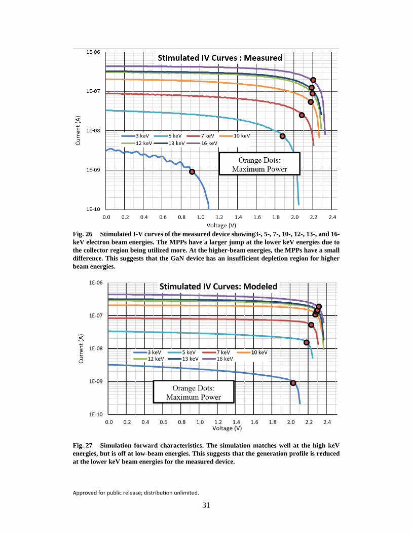
The results from the electron beam stimulated model are shown in Figs. 26 and 27. These can be compared to the I-V curves resulting from the measured device shown in Figs. 26 and 27. The maximum power points are denoted as orange circles in the figures. The difference between the maximum power points with increasing beam energy is shown to decrease.
1.00E-13
1.00E-12
1.00E-11
1.00E-10
1.00E-09
3 4 5 6 7 8 9 10 11 12 13 14 15 16
Curr
ent(
A)
Electron Beam Energy (keV)
Input Beam Currents: Measured vs Modeled
Simulation Input Beam Current (A)Guassian Beam Caluated Beam Currents (A)
Approved for public release; distribution unlimited.
31
Fig. 26 Stimulated I-V curves of the measured device showing3-, 5-, 7-, 10-, 12-, 13-, and 16-keV electron beam energies. The MPPs have a larger jump at the lower keV energies due to the collector region being utilized more. At the higher-beam energies, the MPPs have a small difference. This suggests that the GaN device has an insufficient depletion region for higher beam energies.
Fig. 27 Simulation forward characteristics. The simulation matches well at the high keV energies, but is off at low-beam energies. This suggests that the generation profile is reduced at the lower keV beam energies for the measured device.

Approved for public release; distribution unlimited.
32
Fig. 28 The stimulated forward I-V curve for the 5- and 16-keV experiment. The measured device and modeled device I-V curves are compared. At the lower energy range (5 keV) the metal contact (discussed in Section 6) has more impact on the resulting EHP profile, which serves as the initial condition for the simulation.
As shown in Figs. 26–28, the short circuit currents are the same magnitude; however, the slope of the knee voltage for the measured and simulated devices are different. This effect is due to the EHP generation profile within the device and the diffusion collection within the device. A conclusion is drawn from the fact that through the operation of a betavoltaic or photovoltaic, the electric field within the semiconductor device shrinks with increasing voltage. Due to the poor quality of the GaN material used in the device, the diffusion length was small as described in Section 3.1.4. This resulted in the collection of EHPs in the device being controlled by the depletion region. The depletion region will shrink to the junction between the P region and the intrinsic region. At some point, the internal depletion region will shrink, at which the point the device “turns” on (Fig. 29).
1E-09
1E-08
1E-07
1E-06
0.0 0.2 0.4 0.6 0.8 1.0 1.2 1.4 1.6 1.8 2.0 2.2 2.4
Inve
rted
Cur
rent
(A)
Voltage (V)
Stimulated IV Curve Comparison : Modeled vs. Measured
5 keV Measured
16 keV Measured
5 keV Simulated
16 keV Simulated

Approved for public release; distribution unlimited.
33
Fig. 29 Depletion region shrinking with voltage across the betavoltaic. As the depletion region shrinks, so does the effective collection region.
The resulting voltage slope is seen in the behavior of the diode. As the 3-keV I-V curve for the measured device has an open circuit voltage of 1.1 V, we can establish that at 1.1 V all the internal current mechanisms are equal and opposite, with minimal EHP collection occurring. This suggests that the 3-keV EHP generation profile does not reach into the device as deeply as the simulated model used, which means that the EHP generation for the actual device was shifted closer to the p-type region. There is less difference between the measured device and the model at the higher keV beams, which suggests that the EHP generation profile with respect to electron range between the measured and simulation are more similar. This suggests that something is attenuating the low-energy electrons, and slightly impedes the high-energy electrons, which is characteristic of metal. This may be from an absence of metal included within the device, and is discussed more in Section 5.
The maximum power point of the measured and modeled I-V curve results also show how the effective depletion region controls the power out of the device. The MPPs for the measured device and the model are shown in Fig. 30. For electron beam energies below approximately 6 keV, the MPPs increase with a high slope. This is due to the electron range of the incoming electrons being stopped before the end of the depletion region, resulting in all of the energy deposition being within the depletion region. As the electrons had increased energy, more energy was deposited in a greater depletion region volume. When the electron beam energy was increased past 6 keV, the electron range within the semiconductor range increased to where energy deposition occurred past the depletion region. This meant that at the higher keV electrons, the depletion region only had more energy deposition through the higher-energy electrons, and not through additional use of its volume. After the depletion region was filled, the MPP had diminishing returns with increasing electron beam energy. To optimize the performance of a GaN betavoltaic

Approved for public release; distribution unlimited.
34
converter, the depletion region volume must be matched to the volume of the energy deposition of the incoming beta radiation. Any electron that goes past the collection region is wasted energy, which lowers efficiency of the energy conversion.
Fig. 30 Maximum Power Point comparison between the modeled and measured data is calculated. The difference in MPP values is greater for low-energy electron beams because electron range is better matched to depletion.
5. Conclusions
The model and simulation of a GaN betavoltaic device was shown. The model was found by using parameters from prior research and literature resources. The model illuminated areas that need to be optimized for betavoltaic operation and areas that still require further research. The GaN material properties were found using a sweep over the values of the parameter. The minority carrier lifetime was found by matching the I-V curve results of the measured device with a value of 10–12 s, which shows that current GaN fabrication technology inhibits betavoltaic operation. The collection of EHPs due to diffusion was insignificant due to the poor minority carrier lifetime of the device, resulting in a diffusion length less than 100 nm. The poor minority carrier lifetime resulted from SRH recombination, due to the traps within the device. Thus, the collection of EHPs that contribute to current is dominated by the depletion region collection. This is corroborated from the stimulated I-V curve results, as the MPPs show that the increase of maximum power is not linear. The change in slope of the MPP matches with the electron beam range extending past the depletion region for the varying electron energies. As the fabrication of GaN with less traps is not yet possible, to optimize a GaN device for
1E-9
1E-8
1E-7
1E-6
3 4 5 6 7 8 9 10 11 12 13 14 15 16
Max
imum
Pow
er O
ut (W
)
Input Beam Energy (keV)
Maximum Power Points : Measured vs. Modeled
MPP - Simulated
MPP - Measured
Filling theDepletion Region
SaturatedDepletion Region

Approved for public release; distribution unlimited.
35
betavoltaic operation means matching the depletion region to the energy deposition resulting from radiation. Improving short circuit current can be achieved through extending the depletion region volume to the energy deposition profile. Improving the MPP can be achieved by having the p-n junction placed where the peak of the energy deposition profile occurs. The difference between the model and measured device I-V currents is suspected to be according to the metal contact of the device blocking the input electron beam. The impact of the metal contact reduces the effective EHP generation within the depletion region, especially at the lower keV electron energies. A more recent series of MCNPX calculations that include a 255-nm metal contact region on top of the GaN p-type has (at the time of this writing) produced a modified set of energy profiles that more accurately describe the resulting EHP generation profiles. A new set of Silvaco ATLAS simulations will be numerically calculated based on this new physical configuration. These new energy deposition profiles should more accurately match the measured device I-V curves. The new energy deposition given by MCNPX is shown in Fig. 31.
Fig. 31 The energy deposition profile, numerically calculated, is shown for a 255-nm contact layer on top of the GaN. The contact layer covers 25% of the experimental device. Electrons below 10 keV are stopped within the contact layer.
The first phase of our investigation of material parameters was through a direct comparison to the measured device dark current. It became clear that the depletion region formed by the internal electric field was found to be 500 nm in width. A variety of material parameters were investigated that affect the operation of a betavoltaic energy converter, providing insight into limitations in GaN growth techniques for future device fabrication. The minority carrier lifetime is the
-0.2 0 0.2 0.4 0.6 0.8 1 1.2 1.40
0.5
1
1.5
2
2.5x 10
6
Distance (um)
E (MeV
/cc)
/e- in
c
Beta Energy Deposition/incident electron air
-2345678910111213141516

Approved for public release; distribution unlimited.
36
parameter that affects operation the most, directly driving diffusion collection. SRH recombination is, thus, the most important parameter to find. Radiative and surface recombination were found to have negligible effect, and will continue to be negligible until the SRH recombination improves. The tunneling effective mass was shown to greatly change the electron beam stimulated current result; however, the default value of 0.25 mo provides the optimum fit to data. The shunt resistance for a device is a macroscopic parameter that includes both material properties and surface effects. The modeling parameter Rsh (2.7 GΩ) that best matched the measured result was identified during the dark current verification phase of this research and was used for all following simulations.
The best device efficiency was achieved when the electron range was matched to the depletion region. The model result defining the depletion region on the order of 500 nm, which corresponds to the 6-keV electron range, correlates well with the change in slope of the MPP. The matching of the I-V curves is the best comparison of simulation to experiment. The input electron beam current in the model differs from the measured device experiment, especially at the lower keV electron energies, as it is theorized that the metal contact layer on the p-type GaN preferentially absorbs the lower energy electrons. This produces a larger discrepancy between the model and measured input electron beam current below 10 keV. The next iteration will be to include the effect of the metal contact through changing the EHP generation profile, producing a new set of modeled I-V curves.
The modeling results compare well with measured data and serve to verify the material properties and operation of the GaN energy conversion process. This successful verification now permits the model to be GaN devices with different initial conditions. The simulations to date describe monenergistic electron beams directed towards the GaN device that directly compared to a first set of experimental measured results. The next application of this verified result will be to use a broad beta spectrum that will provide efficiency results (energy conversion) of this device when using the isotopes of 3H and 63Ni. Energy deposition as a function of depth within GaN will be numerically calculated from the beta spectra for 3H and 63Ni, and applied to calculate the performance and efficiency of the GaN device under isotope exposure. These beta spectra will allow investigation into the optimization of GaN betavoltaic device structure. Specifically, 3-D structures that increase the surface area on a wafer footprint will be investigated. Both etched mesa structures and 3D P-i-N pillared GaN structures on a wafer will be investigated for increasing efficiency on a wafer.

Approved for public release; distribution unlimited.
37
6. References
1. Litz M, Russo J, Katsis D. Tritium-powered radiation sensor network. Chemical, Biological, Radiological, Nuclear, and Explosives (CBRNE) Sensing XVII, 2016.
2. Ehrenberg W, Lang C, West R. The electron voltaic effect. Proc Phys Soc A 1951;64(4):424–424.
3. Rappaport P. The electron-voltaic effect in p − n junctions induced by beta-particle bombardment. Phys Rev. 1953;93(1):246–247.
4. Becker A, Kruppke E. Zur Kenntnis des Selenphotoelements. I. Zeitschrift fur Physik. 1937;107(7–8):474–484.
5. Ehrenberg W, Lang C. Probing of barrier layers with an electron beam. Physica. 1954;20(7–12):1137–1138.
6. Loferski J, Rappaport P. Electron-bombardment induced recombination centers in germanium. J Appl Phys. 1959;30(8):1318.
7. Billington E, Ehrengerg W. The electron voltaic effects in silicon and selenium elements. Proc Phys Soc. 1961;78(5):845–853.
8. Windle W. Pm147-silicon betavoltaic battery feasibility. Sandia Corp. TR: SC-RR-65-671, United States, 1966.
9. Olsen L. Betavoltaic energy conversion. Energy Conversion. 1973;13(4):117–127.
10. Olsen L, Seeman S, Griffin B. Betavoltaic nuclear electric power sources. Trans Amer Nucl Soc. 1969;12:481–482.
11. Matheson W. The betavoltaic pacemaker power source. Engineering in Medicine. 1975:401–424.
12. Thomas C, Portnoff S, Spencer M. High efficiency 4H-SiC betavoltaic power sources using tritium radioisotopes. Appl Phys Lett. 2016;108(1):013505.
13. Chandrashekhar M, Thomas C, Li H, Spencer M, Lal A. Demonstration of a 4H SiC betavoltaic cell. Materials Science Forum. 2006;527–529:1351–1354.
14. Da-Yong Q, Wei-Zheng Y, Peng G, Xian-Wang Y, Bo Z, Lin Z, Hui G, Hong-Jian Z. Demonstration of a 4H SiC betavoltaic nuclear battery based on Schottky barrier diode. Chinese Physics Letters. 2008;25(10):3798–3800.

Approved for public release; distribution unlimited.
38
15. Guo H, Shi Y, Zhang Y, Zhang Y, Han J. Fabrication of SiC p-i-n betavoltaic cell with 63Ni irradiation source. 2011 IEEE International Conference of Electron Devices and Solid-State Circuits, 2011.
16. Levinshteĭn M, Rumyantsev S, Shur M. Properties of advanced semiconductor materials. New York: Wiley, 2001, pp. 1–30.
17. Ionascut-Nedelcescu A, Carlone C, Houdayer A, von Bardeleben H, Contin J, Raymond S. Radiation hardness of gallium nitride. IEEE Trans Nucl Sci. 2002;49(6):2733–2738.
18. Klein C. Bandgap dependence and related features of radiation ionization energies in semiconductors. J Appl Phys. 1968;39(4):2029.
19. Concetta A. Device Simulation. Santa Clara: Silvaco, 2010.
20. Pelowitz D. MCNPX user’s manual, 2nd ed. Los Alamos: Los Alamos National Labortory, 2011.
21. Sze S. Physics of semiconductor devices, 2nd ed. New York: Wiley, 1981.
22. Piprek J. Semiconductor optoelectronic devices. Amsterdam (Netherlands): Academic Press; 2003.
23. Ozpineci B. Comparison of wide-bandgap semiconductors for power electronics applications. Washington, D.C.: United States. Dept. of Energy, 2004.
24. Kaminski N. State of the art and the future of wide band-gap devices. Power Electronics and Applications, 2009. EPE '09. 13th European Conference on, Barcelona, 2009, pp. 1–9.
25."NSM Archive - Physical Properties of Semiconductors. Ioffe.ru. [Online]. Available: http://www.ioffe.ru/SVA/NSM/Semicond/. [Accessed: 12- Jul- 2015].
26. Ozgur U, Liu Huiyong, Li Xing, Ni Xianfeng, Morkoc H. GaN-based light-emitting diodes: efficiency at high injection levels. Proceedings of the IEEE. 2010;98(7):1180–1196.
27. Wang X, Wang Z. High-efficiency solar cells. New York: Springer International Publishing, 2013.

Approved for public release; distribution unlimited.
39
28. Mandurrino M, Verzellesi G, Goano M, Vallone M, Bertazzi F, Ghione G, Meneghini M, Meneghesso G, Zanoni E. Physics-based modeling and experimental implications of trap-assisted tunneling in InGaN/GaN light-emitting diodes. Phys Status Solidi A. 2015;212(5):947–953.
29. Olsen L, Cabauy P, Elkind B. Betavoltaic power sources. Phys Today. 2012;65(12):35.
30. Farahmand M, Garetto C, Bellotti E, Brennan K, Gaono M, Ghillino E, Ghione G, Albrecht J, Ruden P. Monte Carlo simulation of electron transport in the III-nitride wurtzite phase materials system: binaries and ternaries. IEEE Trans. Electron Devices. 2001;48(3):535–542.
31. Wang J, Mulligan P, Cao L. Transient current analysis of a GaN radiation detector by TCAD. Nuclear Instruments and Methods in Physics Research Section A: Accelerators, Spectrometers, Detectors and Associated Equipment. 2014;761:7–12.
32. Polyakov A, Lee I, Smirnov N, Govorkov A, Kozhukhova E, Pearton S. Comparison of hole traps in n-GaN grown by hydride vapor phase epitaxy, metal organic chemical vapor deposition, and epitaxial lateral overgrowth. J Appl Phys. 2011;109(12):123701.
33. Py M, Zellweger C, Wagner V, Carlin J, Buehlmann H, Ilegems M. Characterization of deep levels in n-GaN by combined capacitance transient techniques. Phys Stat Aol. (A). 2005;202(4):572–577.
34. Wickenden A, Koleske D, Henry R, Twigg M, Fatemi M. Resistivity control in unintentionally doped GaN films grown by MOCVD. Journal of Crystal Growth. 2004;260(1–2):54–62.
35. Pearton S, Abernathy C, Ren F. Gallium nitride processing for electronics, sensors and spintronics. London: Springer, 2006.
36. Litz M, Ray W, Russo J, Kelley S, Smith J. Planar homojunction GaN P-u-N device evaluated for betavoltaic energy conversion: measurement and analysis. ARL, Adelphi.

Approved for public release; distribution unlimited.
40
INTENTIONALLY LEFT BLANK.
Approved for public release; distribution unlimited.
41
Appendix A. Silvaco GaN Dark Current Input Deck

Approved for public release; distribution unlimited.
42
The following input deck is the final version used for dark current generation shown in Fig. 20 described in Section 3.2.5. This input deck differs from that described in Appendix D only by emission of the initial conditions of EHP.
go atlas simflags="-160 -P 16" #The simflags are setup for 160 bit precision and using 16 processors. #The setting of the Z direction of the device - In this case for 100 micron by 100 micron. This value is a scalar multiplier mesh width=100 #mesh setup - The values are all in micron #x mesh values and spacing x.m l=0 s=1 x.m l=100 s=1 x.m l=100 s=1 x.m l=104 s=1 #y mesh values and spacing y.m l=0 s=0.001 y.m l=0.06 s=0.001 y.m l=0.075 s=0.001 y.m l=0.085 s=0.001 y.m l=0.1 s=0.005 y.m l=1.06 s=0.005 y.m l=1.075 s=0.001 y.m l=1.085 s=0.001 y.m l=1.1 s=0.5 y.m l=3.08 s=0.5 #Setting the regions of the device – GaN, Insulator, and Shunt Resistance #The GaN Material is set from 0 to 100 micron region num=1 mat=GaN #The insulator is set to 100 to 102 micron region num=2 x.min=100 x.max=102 insulato #The shunt resistance is set from 102 to 104 micron region num=3 material=Aluminum x.min=102 x.max=104 conductor #Electrodes – The connection to the device. The widths are set to match the active area of the device electr name=anode top x.min=12.5 x.max=87.5 electr name=cathode bot x.min=12.5 x.max=87.5 electr name=restop top x.min=102 x.max=104 electr name=resbot bot x.min=102 x.max=104 #Doping #Intrinsic Region doping n.type conc=1e16 x.min=0 x.max=100 y.min=0 y.max=1.08 uniform #P+ region doping p.type conc=4e17 x.min=0 x.max=100 gauss junction=0.08 #N+ region doping n.type conc=3e18 x.min=0 x.max=100 y.min=1.08 y.max=3.08 uniform #Material Parameters of the device #Retrieve the default set from Silvaco for GaN material num=1 kp.set1 #Set the SRH minority carrier lifetime for electrons and holes material num=1 taun0=1e-12 taup0=1e-12

Approved for public release; distribution unlimited.
43
#Set the conductor region to be highly resistive, to simulate a equivalent shunt resistance material material=Aluminum resistivity=1.763e13 #GaN material deep level traps trap mat=GaN donor e.level=0.55 density=2.4e14 sign=2.7e-12 sigp=2.7e-12 degen=1 trap mat=GaN donor e.level=0.65 density=2.1e14 sign=1.7e-14 sigp=1.7e-14 degen=1 trap mat=GaN donor e.level=0.85 density=3.4e14 sign=1.8e-13 sigp=1.8e-13 degen=1 trap mat=GaN donor e.level=1.20 density=2.9e15 sign=4.7e-14 sigp=4.7e-14 degen=1 trap mat=GaN acceptor e.level=3.26 density=1e14 sign=2.3e-17 sigp=2.3e-17 degen=1 trap mat=GaN acceptor e.level=2.91 density=9e14 sign=3.3e-16 sigp=3.3e-16 degen=1 trap mat=GaN acceptor e.level=2.90 density=5.8e14 sign=3.3e-17 sigp=3.3e-17 degen=1 trap mat=GaN acceptor e.level=2.49 density=5.8e15 sign=1e-16 sigp=1e-16 degen=1 #Simulation models used models material=GaN srh fermi fldmob print optr trap.tunnel mass.tunnel=0.25 #Mobility models for GaN, low field and high field mobility material=GaN fmct.n chen.n chen.p #Fermi calculation of intrinsic carriers models material=GaN ni.fermi method maxtrap=100 #Setup the series resistance connection contact name=anode resistance=3.72 ohms #Setup the parallel connection to the shunt resistance contact name=restop common=anode short contact name=resbot common=cathode short #Solve for Zero Bias solve init #Save the structure file #save outf=dark.str #Sweep the voltage of the device and record the data log outf=$"kev"_$"id"_$"trial_id"_$"trap".log csv=$"kev"_$"id"_$"trial_id"_$"trap".csv solve vanode=0 vstep=0.02 vfinal=2.5 name=anode cname=anode log off quit

Approved for public release; distribution unlimited.
44
INTENTIONALLY LEFT BLANK.

Approved for public release; distribution unlimited.
45
Appendix B. MCNPX Input Deck

Approved for public release; distribution unlimited.
46
The following input deck is an example of the numerical calculation described in Section 2.2, which calculates the energy deposition profiles from which the EHP profiles are developed.
Model of GaN-DEC 7keV electron beam c c +------------------------------------------------------+ c | Cell Cards | c +------------------------------------------------------+ c # mat density surface data 2 4 -6.15 -2 imp:e,p 1 u=1 $GaN backsplash 21 2 -.00129 -21 imp:e,p 1 u=1 $air 3 4 -6.15 -3 imp:e,p 1 u=1 $GaN p-layer 4 4 -6.15 -4 imp:e,p 1 u=1 $GaN i-layer 5 4 -6.15 -5 imp:e,p 1 u=1 $GaN n-1st layer 6 4 -6.15 -6 imp:e,p 1 u=1 $GaN n-2nd layer 7 4 -6.15 -7 imp:e,p 1 u=1 $GaN n-3rd layer 8 4 -6.15 -8 imp:e,p 1 u=1 $GaN n-4th layer 9 4 -6.15 -9 imp:e,p 1 u=1 $GaN 10 4 -6.15 -10 imp:e,p 1 u=1 $GaN 11 4 -6.15 -11 imp:e,p 1 u=1 $GaN 12 4 -6.15 -12 imp:e,p 1 u=1 $GaN 41 4 -6.15 -41 imp:e,p 1 u=1 $GaN p-layer 42 4 -6.15 -42 imp:e,p 1 u=1 $GaN p-layer 43 4 -6.15 -43 imp:e,p 1 u=1 $GaN p-layer 44 4 -6.15 -44 imp:e,p 1 u=1 $GaN p-layer 45 4 -6.15 -45 imp:e,p 1 u=1 $GaN p-layer 46 4 -6.15 -46 imp:e,p 1 u=1 $GaN p-layer 47 4 -6.15 -47 imp:e,p 1 u=1 $GaN p-layer 48 4 -6.15 -48 imp:e,p 1 u=1 $GaN p-layer 49 4 -6.15 -49 imp:e,p 1 u=1 $GaN p-layer c air encasing 33 2 -0.00129 -33 2 3 4 5 6 7 8 9 10 11 12 21 & 41 42 43 44 45 46 47 48 49 imp:e,p 1 u=1 34 0 33 imp:e,p 1 u=1 c room 35 2 -0.00129 -34 imp:e,p 1 fill=1 36 0 34 imp:e,p 0 $outside world c +------------------------------------------------------+ c | Surface Cards | c +------------------------------------------------------+ 2 rpp -0.005 0.005 -0.0001 -0.00006 -0.005 0.005 $GaN 21 rpp -0.005 0.005 -0.00006 0.0000 -0.005 0.005 $GaN 3 rpp -0.005 0.005 0.00000 0.00001 -0.005 0.005 $GaN 100x100um 2um 4 rpp -0.005 0.005 0.00001 0.00002 -0.005 0.005 $GaN 5 rpp -0.005 0.005 0.00002 0.00003 -0.005 0.005 $GaN 6 rpp -0.005 0.005 0.00003 0.00004 -0.005 0.005 $GaN 7 rpp -0.005 0.005 0.00004 0.00005 -0.005 0.005 $GaN 8 rpp -0.005 0.005 0.00005 0.00006 -0.005 0.005 $GaN 9 rpp -0.005 0.005 0.00006 0.00007 -0.005 0.005 $GaN 10 rpp -0.005 0.005 0.00007 0.00008 -0.005 0.005 $GaN 11 rpp -0.005 0.005 0.00008 0.00009 -0.005 0.005 $GaN 12 rpp -0.005 0.005 0.00009 0.00010 -0.005 0.005 $GaN 41 rpp -0.005 0.005 0.00010 0.00011 -0.005 0.005 $GaN

Approved for public release; distribution unlimited.
47
42 rpp -0.005 0.005 0.00011 0.00012 -0.005 0.005 $GaN 43 rpp -0.005 0.005 0.00012 0.00013 -0.005 0.005 $GaN 44 rpp -0.005 0.005 0.00013 0.00014 -0.005 0.005 $GaN 45 rpp -0.005 0.005 0.00014 0.00015 -0.005 0.005 $GaN 46 rpp -0.005 0.005 0.00015 0.00016 -0.005 0.005 $GaN 47 rpp -0.005 0.005 0.00016 0.00017 -0.005 0.005 $GaN 48 rpp -0.005 0.005 0.00017 0.00018 -0.005 0.005 $GaN 49 rpp -0.005 0.005 0.00018 0.00019 -0.005 0.005 $GaN c airto encase GaN 33 rpp -0.4 0.4 -0.4 0.4 -0.4 0.4 $encasing air c room dimensions 34 rpp -0.5 0.5 -0.5 0.5 -0.5 0.5 $room air c +------------------------------------------------------+ c | Material Cards | c +------------------------------------------------------+ c m# isotope percent &(newline) $comment m2 8016 .3 7014 .7 $air 0.00129 g/cc m4 31000 .5 7000 .5 $GaN 6.15 g/cc c +------------------------------------------------------+ c | Source Definition | c +------------------------------------------------------+ SDEF POS=0 -.00003 0 RAD=d1 PAR=e ERG=.007 AXS=0 1 0 vec=0 1 0 dir=1 SI1 0 .0001 $ radial sampling range: 0 to Rmax SP1 -21 1 $ radial sampling weighting: r^1 for disk source c +------------------------------------------------------+ c | Data Cards | c +------------------------------------------------------+ mode p e $ n h d t s a these not needed PHYS:P PHYS:E nps 1000000 $ .1Mh~.26min 90Mh~3hr ptrac nps=1,1000 type=e file=asc event=bnk,sur,col,ter,cap c +------------------------------------------------------+ c | Tallies | c +------------------------------------------------------+ fc14 flux averaged over the cell in particles/cm^2 f14:e 2 21 3 4 5 6 7 e14 0 38i .05 fc16 energy deposited averaged over cell MeV/g f16:p 2 21 3 4 5 6 7 e16 0 98i .05 fc26 energy deposited averaged over cell MeV/g f26:e 2 21 3 4 5 6 7 e26 0 38i .05 c +------------------------------------------------------+ c | Mesh | c +------------------------------------------------------+ tmesh rmesh21:e flux pedep cora21 -.005 158i .005 corb21 -.0001 198i .0001 corc21 -.005 .005 c rmesh31:e flux pedep cora31 -.1 158i .1 corb31 -.0004 298i .0004

Approved for public release; distribution unlimited.
48
corc31 -.1 .1 c rmesh41:e flux pedep dose cora41 -.4 158i .4 corb41 -.001 198i .001 corc41 -.4 .4 endmd

Approved for public release; distribution unlimited.
49
Appendix C. Silvaco Gallium Nitride Simulation Parameter List

Approved for public release; distribution unlimited.
50
Silvaco contains a set of default simulation parameters for gallium nitride (GaN). The following list of parameters has been modified from the default in order to provide a better match of measured data to simulation results. The modified parameters have been researched and are within presently understood ranges of material quality. The modifications and references are discussed in Section 3.
Material Parameter Abbreviation Units Value Boltzmann’s Constant k J*K–1 1.38066e-23 J/K Elementary charge q C 1.60219e-19 C Permittivity in vacuum ε0 F*cm–1 8.85419e-14 F/cm Temperature T K 300 K Thermal Voltage VT V 0.025852 V GaN Relative Permittivity
εR - 8.9
Band Gap Eg eV 3.43 Electron Affinity χ eV 3.35 Conduction Band Density of States
NC cm–3 2.24e18
Valence Band Density of States
NV cm–3 2.51e19
Intrinsic Carrier Concentration
ni cm–3 1.06e-10
SRH Electron Carrier Lifetime
τn s 1e-12
SRH Hole Carrier Lifetime
τp s 1e-12
Auger Recombination Coefficients
- - Ignored
Optical Capture Rate COPT cm3*s–1 1.1e-8 Electron rest mass m0 kg 9.109e-31 kg Effective Mass of Tunneling
meff m0 0.25
Electron Tunneling Effective Mass
met m0 0.20
Hole Tunneling Effective Mass
mpt m0 1
Electron Thermal Velocity
vn cm*s–1 2.61e+07
Hole Thermal Velocity vp
cm*s–1 1.17e+07
Electron Saturation Velocity
vsat.n cm*s–1 1.9e7
Hole Saturation Velocity
vsat.p cm*s–1 1.4e7
Shunt Resistance Rshunt Ω 2.76e9 Series Resistance Rseries Ω 3.72

Approved for public release; distribution unlimited.
51
Appendix D. Silvaco GaN Stimulated Input Deck

Approved for public release; distribution unlimited.
52
The Silvaco input deck that follows first describes the mesh structure, the material regions, the contact electrode points, doping concentrations, material properties (parameters), which physics modules to include, and series resistance. The I-V curve is then generated and saved in a file for this 3-keV applied beam example.
go atlas simflags="-160 -P 16" #The simflags are setup for 160 bit precision and using 16 processors. #The setting of the Z direction of the device - In this case for 100 micron by 100 micron. This value is a scalar multiplier mesh width=100 #mesh setup - The values are all in micron #x mesh values and spacing x.m l=0 s=1 x.m l=100 s=1 x.m l=100 s=1 x.m l=104 s=1 #y mesh values and spacing y.m l=0 s=0.001 y.m l=0.06 s=0.001 y.m l=0.075 s=0.001 y.m l=0.085 s=0.001 y.m l=0.1 s=0.005 y.m l=1.06 s=0.005 y.m l=1.075 s=0.001 y.m l=1.085 s=0.001 y.m l=1.1 s=0.5 y.m l=3.08 s=0.5 #Setting the regions of the device – GaN, Insulator, and Shunt Resistance #The GaN Material is set from 0 to 100 micron region num=1 mat=GaN #The insulator is set to 100 to 102 micron region num=2 x.min=100 x.max=102 insulato #The shunt resistance is set from 102 to 104 micron region num=3 material=Aluminum x.min=102 x.max=104 conductor #Electrodes – The connection to the device. The widths are set to match the active area of the device electr name=anode top x.min=12.5 x.max=87.5 electr name=cathode bot x.min=12.5 x.max=87.5 electr name=restop top x.min=102 x.max=104 electr name=resbot bot x.min=102 x.max=104 #Doping #Intrinsic Region doping n.type conc=1e16 x.min=0 x.max=100 y.min=0 y.max=1.08 uniform #P+ region doping p.type conc=4e17 x.min=0 x.max=100 gauss junction=0.08 #N+ region doping n.type conc=3e18 x.min=0 x.max=100 y.min=1.08 y.max=3.08 uniform #Material Parameters of the device #Retrieve the default set from Silvaco for GaN material num=1 kp.set1 #Set the SRH minority carrier lifetime for electrons and holes material num=1 taun0=1e-12 taup0=1e-12

Approved for public release; distribution unlimited.
53
#Set the conductor region to be highly resistive, to simulate a equivalent shunt resistance material material=Aluminum resistivity=1.763e13 #GaN material deep level traps trap mat=GaN donor e.level=0.55 density=2.4e14 sign=2.7e-12 sigp=2.7e-12 degen=1 trap mat=GaN donor e.level=0.65 density=2.1e14 sign=1.7e-14 sigp=1.7e-14 degen=1 trap mat=GaN donor e.level=0.85 density=3.4e14 sign=1.8e-13 sigp=1.8e-13 degen=1 trap mat=GaN donor e.level=1.20 density=2.9e15 sign=4.7e-14 sigp=4.7e-14 degen=1 trap mat=GaN acceptor e.level=3.26 density=1e14 sign=2.3e-17 sigp=2.3e-17 degen=1 trap mat=GaN acceptor e.level=2.91 density=9e14 sign=3.3e-16 sigp=3.3e-16 degen=1 trap mat=GaN acceptor e.level=2.90 density=5.8e14 sign=3.3e-17 sigp=3.3e-17 degen=1 trap mat=GaN acceptor e.level=2.49 density=5.8e15 sign=1e-16 sigp=1e-16 degen=1 #Simulation models used models material=GaN srh fermi fldmob print optr trap.tunnel mass.tunnel=0.25 #Setup the EHP generation using the C-interpreter beam num=1 f.radiate="../Library/newest/3k2.lib" #Mobility models for GaN, low field and high field mobility material=GaN fmct.n chen.n chen.p #Fermi calculation of intrinsic carriers models material=GaN ni.fermi method maxtrap=100 #Setup the series resistance connection contact name=anode resistance=3.72 ohms #Setup the parallel connection to the shunt resistance contact name=restop common=anode short contact name=resbot common=cathode short #Solve for Zero Bias solve init #Save the dark structure file #save outf=3kdark.str #Incrementally solve the EHP generation solve b1=0.000005 solve b1=0.00001 solve b1=0.00005 solve b1=0.0001 solve b1=0.0005 solve b1=0.001 solve b1=0.005 solve b1=0.01 solve b1=0.05 solve b1=0.1 solve b1=0.2 solve b1=0.3 solve b1=0.4 solve b1=0.5 solve b1=0.6 solve b1=0.7 solve b1=0.8 solve b1=0.9 solve b1=1

Approved for public release; distribution unlimited.
54
#Save the resulting EHP generated Zero Bias structure #save outf=3klight.str #Sweep the voltage of the device and record the data log outf=$"kev"_$"id"_$"trial_id"_$"trap".log csv=$"kev"_$"id"_$"trial_id"_$"trap".csv solve vanode=0 vstep=0.02 vfinal=2.5 name=anode cname=anode log off quit

Approved for public release; distribution unlimited.
55
Appendix E. Silvaco GaN Stimulated EHP Library File

Approved for public release; distribution unlimited.
56
This subroutine defines the appropriate EHP profile. This routine is then called by the input deck in Appendix D. The EHP profile is calculated from the numerically calculated energy deposition profile from MCNPX model described in Section 2.2. An EHP profile is created for each electron beam energy modeled in MCNPX. The polynomial fit for the EHP profile is shown in Table E-1.
#include <stdio.h> #include <stdlib.h> #include <math.h> #include <ctype.h> #include <malloc.h> #include <string.h> #include <template.h> /* * Generation rate as a function of position * Statement: BEAM * Parameter: F.RADIATE * Arguments: * x location x (microns) * y location y (microns) * z location z (microns) * t time (seconds ) * *rat generation rate per cc per sec. */ int radiate(double x,double y,double z,double t,double *rat) double result; if (x<=100) result=2*4.121e8*5*(-304001008413440.00*y*y*y*y+183780067386441.00*y*y*y-33851276701993.40*y*y+1307022366666.75*y+109053865855.30); if(result > 0) *rat=result; else *rat=0; else *rat=0; return(0); /* 0 - ok */ quit

Approved for public release; distribution unlimited.
57
Table E-1 Shown are the polynomial coefficients for several keV beam stimulus. The equations are normalized to create 100 EHPs within the volume, according to the device mesh points of the device.
Polynomial coefficients keV y^6 y^5 y^4 y^3 y^2 y C
3 -458573179311587000*y^6
+286710045899686000*y^5
-70433127905612800*y^4
+8365907246343810*y^3
-455502620849616*y^2
+6026791261804*y
+220572891679.18
5 X X -304001008413440.00*y^4
+183780067386441.00*y^3
-33851276701993.40*y^2
+1307022366666.75*y
+109053865855.3
7 -27241408510169.9*y^6
86473917112308.9*y^5
-105849514904224
+61853616283935.5*y^3
-16884135254336.8*y^2
+1551153280496.61*y
55422075747.59
10 X X -4637320985175.81*y^4
+7972259061172.25*y^3
-4495821808680.92*y^2
+759694191629.89*y
+44322999156.47
12 X X -995935552050.93*y^4
+2423458616521*y^3
-1908353757824.08*y^2
+436561512201.32*y
+41142132335.39
13 X X -683566560252.92*y^4
+1774987893346.08*y^3
-1516263210648.57*y^2
+386101980388.01*y
+37226813101.87
16 X X -369750609033.05*y^4
+995506634113.31*y^3
-946885175146.33*y^2
+298460996259.80*y
+27598060001.42

Approved for public release; distribution unlimited.
58
List of Symbols, Abbreviations, and Acronyms
3H Tritium 63Ni Nickel-63
2D 2-Dimensional
3D 3-Dimensional
4H-SiC 4 Hydrogen – Silicon Carbide
Al2O3 Sapphire
C Diamond
COPT Optical Capture Rate
DC Direct current
DEC Direct energy conversion
EBIC Electron beam-induced current
EHP Electron-hole pair
eV Electron volts
FMCT Farahmand Modified Caughey Thomas
GaAs Gallium Arsenide
GaN Gallium Nitride
GaP Gallium Phosphide
Ge Germanium
IDEC Indirect energy conversion
LED Light Emitting Diode
Mg Magnesium
MOCVD Metal-Organic Chemical Vapor Deposition
MPP Maximum Power Point
Si Silicon
SiC Silicon Carbide

Approved for public release; distribution unlimited.
58
Sr Strontium
SRH Shockley-Reed-Hall
TCAD Technology computer-aided design

Approved for public release; distribution unlimited.
59
1 DEFENSE TECH INFO CTR (PDF) DTIC OCA 2 US ARMY RSRCH LAB (PDF) IMAL HRA MAIL & RECORDS MGMT RDRL CIO LL TECHL LIB 1 GOVT PRNTG OFC (PDF) A MALHOTRA 3 US ARMY RSRCH LAB (PDF) RDRL SED E J RUSSO M LITZ W B RAY II

Approved for public release; distribution unlimited.
59
INTENTIONALLY LEFT BLANK.