modeling and development of a bridgeless pfc boost...
TRANSCRIPT

9
G. E. Mejía-Ruiz et al.; Revista Facultad de Ingeniería, No. 82, pp. 9-21 2017
Modeling and development of a bridgeless PFC Boost rectifier
ABSTRACT: This paper proposes a model of the bridgeless PFC (Power Factor Correction) boost rectifier for control purposes based on an averaged small-signal analysis. From circuital laws, four operation modes are defined and explained, ensuring a relationship of physical variables in the converter. Based on the proposed model, two-loop cascade control structures composed of Proportional-Integral (PI) lineal controllers are proposed. Design consideration for dimensioning reactive elements is included, providing minimum values for their inductance and capacitance. Implementation of a laboratory prototype of 900 W and experimental results are presented to validate and reaffirm the proposed model. Experimental results demonstrate that the use of the bridgeless PFC boost converter model allows the Power Factor (PF) to be elevated up to 0.99, to reduce the THDi (Total Harmonic Distortion of the Current) to 3.9% and to control the DC voltage level on output. Compliance of standards of power quality EN 61000-3-2 (IEC 1000-3-2) are experimentally verified.
RESUMEN: Este artículo propone un modelo para rectificadores elevadores PFC (Power Factor Correction por sus siglas en inglés) sin puente para propósitos de control y basado en el análisis del promedio de pequeña señal. A partir de las leyes circuitales, cuatro modos de operación son definidos y explicados, asegurando una relación entre las variables físicas del convertidor. Basados en el modelo propuesto, dos lazos cerrados de control compuestos por controladores lineales Proporcionales e Integrales (PI) son propuestos. Algunas consideraciones de diseño para dimensionar los elementos reactivos son incluidas, de tal forma que se obtienen valores mínimos para su inductancia y capacitancia. Se presenta la implementación de un prototipo de 900 W con resultados experimentales que permite validar y reafirmar el modelo propuesto. Los resultados experimentales demuestran que el uso del convertidor PFC permite elevar el factor de potencia FP a 0,99 o más y reducir el THDi (Total Harmonic Distortion of the Current por sus siglas en Inglés) a 3,9 %, además de controlar el bus DC en la salida. Se verifica experimentalmente que el convertidor PFC desarrollado está de acuerdo con los estándares de calidad de la potencia EN 61000-3-2 (IEC 1000-3-2).
* Corresponding author: Nicolás Muñoz Galeanoe-mail: [email protected] 0120-6230e-ISSN 2422-2844
ARTICLE INFOReceived May 05, 2016 Accepted January 26, 2017
KEYWORDSBridgeless power factor correction (PFC), single-phase rectifier bridgeless, mathematical model, PFC boost rectifier
Corrección de factor de potencia (PFC), rectificador sin puente monofásico, modelo matemático, rectificador elevador PFC
Revista Facultad de Ingeniería, Universidad de Antioquia, No. 82, pp. 9-21, 2017
DOI: 10.17533/udea.redin.n82a02
Modelamiento y desarrollo de un rectificador Boost PFC sin puenteGabriel Eduardo Mejía-Ruiz, Nicolás Muñoz-Galeano, Jesús María López-Lezama
Grupo de Manejo Eficiente de la Energía (GIMEL), Departamento de Ingeniería Eléctrica, Facultad de Ingeniería, Universidad de Antioquia. Calle 67 # 53-108. A. A. 1226. Medellín, Colombia.
1. IntroductionAC-DC power converters, also known as rectifiers, allow obtaining direct current from an AC power source. Rectifiers are widely used in applications such as consumer electronics products, switching power supplies, uninterrupted power supplies and charging systems for hybrid vehicles [1, 2]. Usually, conventional rectifiers are reliable and easy to design. These rectifiers are composed of a full bridge-diode and a capacitor. The capacitor charge leads to current peaks in the source; consequently, the use of conventional rectifiers in AC distribution systems is
responsible for increments in the THDi, reducing the Power Factor PF and efficiency of distribution networks [1, 2].
An increase of the THDi in distribution networks can lead to higher power losses in cables, transformers and generators. Besides, a high THDi can cause the magnification of resonant currents, failures in protection devices, and degradation of voltage waveform in large-impedance lines [2-4].
Compliance of power quality standards such as IEEE 519-20142 [5] and IEC 61000-3-2 suggests decreasing the THDi, improving the PF and reducing the Electromagnetic Interference (EMI) [6].
The reduction of the THDi and increase in PF at the source can be achieved by using passive filters or controlled rectifiers. Usually, passive filters are tuned LC filters [7]. Capacitors and inductors used in such filters exhibit high

10
G. E. Mejía-Ruiz et al.; Revista Facultad de Ingeniería, No. 82, pp. 9-21, 2017
cost, volume and weight [8]. Moreover, controlled rectifiers are more efficient than passive filters. These rectifiers operate based on power switches and have one or more closed-loop control systems [9]. Controlled rectifiers can regulate PF, reduce THDi and control DC voltage at the load [8,10,11].
Some AC-DC controlled converters with PFC reported by technical literature are: conventional boost rectifier composed of diodes bridge and boost converter [12-14], AC-DC interleaved boost converter [15, 16], and bridgeless boost PFC converter [17-19].
Conventional boost rectifier is the most common topology among the AC-DC converters [2, 16]. It offers a simple way to achieve high PF and regulated output voltage. Nevertheless, losses from the diode bridge rectifier are significant, particularly at lower input voltage and high output [3].
The bridgeless PFC boost converter has one semiconductor less in the line-current path from source to load, reducing power losses and improving efficiency, in comparison with conventional boost rectifier [20]. The bridgeless PFC boost converter can supply up to 3.5 kW of power to the load and can reduce the ripple voltage in load and the ripple current in source. Moreover, inductors are located on the AC side facilitating its design and EMI filtering [17-22].
A literature review of the bridgeless PFC boost converter and some experimental tests have been reported in [2]. A comparative evaluation of conventional boost rectifier, AC-DC interleaved PFC boost converter and bridgeless PFC boost converter has been presented in [1]. This work demonstrated experimentally that the bridgeless PFC boost converter is more efficient than conventional boost rectifiers. In [17, 18], an improved bridgeless PFC boost topology is proposed to reduce common mode noise. A novel technique for measuring the source current and implementation of the bridgeless PFC boost converter prototype has been introduced in [23]. A calculation of switching losses and an experimental development of the bridgeless PFC boost converter have been explained and analyzed in [21]. An analysis of the THDi and a laboratory prototype of the bridgeless PFC boost converter have been presented in [23]. A topology with soft switching, a control strategy and an experimental approach of bridgeless PFC boost have been proposed in [3].
Although a great variety of studies have been conducted regarding the design of bridgeless PFC boost converter, the reviewed technical literature does not report the phenomenological modeling of the bridgeless PFC boost converter that allows model-based controller design, sizing of components, and analysis of its dynamics, as well as losses and performance in extreme conditions.
This paper proposes an averaged small-signal model for the bridgeless PFC boost converter that allows knowing the dynamic performance of the converter prior to its experimental implementation and the systematic design of the control system. This modeling approach could easily be
generalized to other converter topologies [24]. In addition, this paper presents the principle of operation, control system design, design equations, implementation of a laboratory prototype of 900 W and experimental results that corroborate the theoretical approaches.
In this paper, the operating principle of the bridgeless PFC boost converter is studied in section II. The averaged large-signal and averaged small-signal model of the bridgeless PFC boost converter are proposed in section III and IV, respectively. The design of control systems is presented in section V. Design considerations and experimental results are given in section VI and VII, respectively. Finally, conclusions are presented in section VIII.
2. Operating PrincipleThis section presents the operating principle and mathematical model of the bridgeless boost PFC converter. This model represents the relationship of physical variables in the power converter. Power converters switches work in cut-off and saturation regions; consequently, the bridgeless PFC boost converter exhibits a nonlinear and time-varying dynamic behavior [24, 25].
The bridgeless PFC boost converter presented in this study works in Continuous Conduction Mode (CCM). Figure 1 shows the bridgeless PFC boost converter topology. This topology is composed of two power switches Q1 and Q2, two fast switching diodes D1 and D2, two conventional rectifier diodes D3 and D4, two inductors with same values L1 and L2, a capacitor C, and a load RL [17-19].
Figure 1 Bridgless PFC boost converter topology
The proposed bridgeless PFC boost converter model is obtained based on Kirchhoff’s and Ohm’s laws, and the commutation states of switches Q₁ and Q2. Then, the averaged large-signal model is achieved averaging the switched model on one switching period [26]. Subsequently, the model is linearized using small variations around an operating point, obtaining the small-signal model. Finally, the model is transformed into the state-space and S domain [25, 26].
+
-+
-+
-𝑣𝑣𝑠𝑠 𝐿𝐿 2
𝐿𝐿 1
𝐷𝐷 3 𝐷𝐷 4𝑄𝑄 1 𝑄𝑄 2
𝐶𝐶 𝑅𝑅 𝐿𝐿
𝐷𝐷 1 𝐷𝐷 2𝑛𝑛
𝒊𝒊 𝒔𝒔

11
G. E. Mejía-Ruiz et al.; Revista Facultad de Ingeniería, No. 82, pp. 9-21 2017
Enhancing the accuracy of the model adds complexity to it; increasing the time required for the simulation and the complexity of the control system design. Moreover, increasing the model complexity does not provide significant information about the dominant dynamic behavior of the converter [27-29]. Consequently, the model proposed in this paper is obtained based on the next simplifying assumptions: 1) switches are considered “ideal”, i.e. they have zero-value resistance during conduction and infinite-value resistance when the switch is turned off; 2) switching time is infinitely short; 3) sources are considered “ideal”, i.e. the voltage source provides infinite short circuit power;3) passive elements are considered linear, time-invariantand without parasitic series resistance; and 4) switchingfrequency is much higher than input voltage frequency, i.e.amplitude variations in the source are not significant in oneswitching period (TSW).
The bridgeless PFC boost converter has four operating modes. The controlled commutation of Q1 and Q2 during positive and negative half cycles of the AC input voltage allows output voltage regulation and input current tracking control. Figure 2 shows the four operating modes of the bridgeless PFC boost converter.
Next section describes the operating modes of the bridgeless PFC boost converter and the equations that compose the switched model.
2.1. Operating Mode 1
In operating mode 1, the input voltage (vs) is positive and Q1 is turned on; moreover, Q1 and D₄ are directly polarized. Input current (is) increases exponentially, storing energy in inductor L1. Simultaneously, C supplies power to the load (RL), reducing the output voltage (vc). The current of the capacitor (ic) is assumed positive when it charges the capacitor. The mathematical relationship of voltages and currents in the equivalent circuit for operating mode 1 is given by Eqs. (1) and (2):
(1)
(2)
+
-+
-+
-𝑣𝑣𝑠𝑠 + -𝐿𝐿 1
𝐷𝐷 4𝑄𝑄 1
𝐶𝐶 𝑅𝑅 𝐿𝐿
𝑛𝑛
𝒗𝒗 𝒔𝒔 > 𝟎𝟎 , 𝑸𝑸 𝟏𝟏 i s o n
+
-+
-+
-𝑣𝑣𝑠𝑠 + -𝐿𝐿 1
𝐷𝐷 4
𝐶𝐶 𝑅𝑅 𝐿𝐿
𝐷𝐷 1𝑛𝑛
Mode 2: 𝒗𝒗 𝒔𝒔 > 𝟎𝟎 , 𝑸𝑸 𝟏𝟏 a n d 𝑸𝑸 𝟐𝟐 o f f
+ +
-+
-𝑣𝑣𝑠𝑠
+ -𝐿𝐿 2
𝐷𝐷 3𝑄𝑄 2
𝐶𝐶 𝑅𝑅 𝐿𝐿
𝑛𝑛
𝒗𝒗 𝒔𝒔 < 𝟎𝟎 , 𝑸𝑸 𝟐𝟐 i s o n
+
-+
-+
-𝑣𝑣𝑠𝑠
+ -𝐿𝐿 2
𝐷𝐷 3
𝐶𝐶 𝑅𝑅 𝐿𝐿
𝐷𝐷 2
𝑛𝑛
Mode 4: 𝒗𝒗 𝒔𝒔 < 𝟎𝟎 , 𝑸𝑸 𝟏𝟏 a n d 𝑸𝑸 𝟐𝟐 o f f
𝒊𝒊 𝒔𝒔𝒊𝒊 𝑳𝑳
𝒊𝒊 𝒔𝒔𝒊𝒊 𝑳𝑳𝒊𝒊 𝑪𝑪
𝒊𝒊 𝒔𝒔 𝒊𝒊 𝑳𝑳 𝒊𝒊 𝒔𝒔 𝒊𝒊 𝑳𝑳𝒊𝒊 𝑪𝑪
+
-+
-+
-+
-
+
-+
-+
-+
-
+
-+
-
+
-+
-
+ - - +
+ - - +
Mode 1:
Mode 3:
Mode 2:
Mode 4:
Figure 2 Operating modes of the bridgeless PFC boost converter
12
G. E. Mejía-Ruiz et al.; Revista Facultad de Ingeniería, No. 82, pp. 9-21, 2017
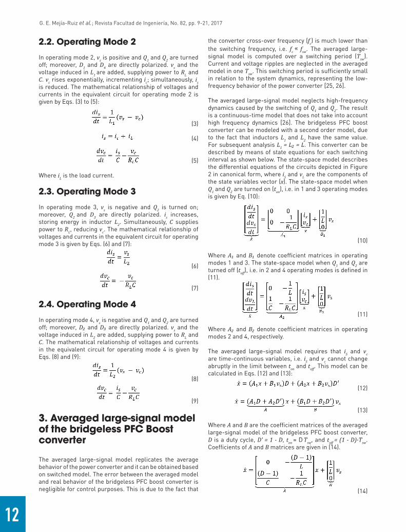
2.2. Operating Mode 2
In operating mode 2, vs is positive and Q1 and Q2 are turnedoff; moreover, D1 and D4 are directly polarized. vs and thevoltage induced in L1 are added, supplying power to RL andC. vc rises exponentially, incrementing ic; simultaneously, isis reduced. The mathematical relationship of voltages andcurrents in the equivalent circuit for operating mode 2 isgiven by Eqs. (3) to (5):
(3)
(4)
(5)
Where iL is the load current.
2.3. Operating Mode 3
In operating mode 3, vs is negative and Q2 is turned on; moreover, Q2 and D3 are directly polarized. is increases, storing energy in inductor L2. Simultaneously, C supplies power to RL, reducing vc. The mathematical relationship of voltages and currents in the equivalent circuit for operating mode 3 is given by Eqs. (6) and (7):
(6)
(7)
2.4. Operating Mode 4
In operating mode 4, vs is negative and Q1 and Q2 are turnedoff; moreover, D₂ and D₃ are directly polarized. vs and thevoltage induced in L2 are added, supplying power to RL andC. The mathematical relationship of voltages and currentsin the equivalent circuit for operating mode 4 is given byEqs. (8) and (9):
(8)
(9)
3. Averaged large-signal modelof the bridgeless PFC Boostconverter
The averaged large-signal model replicates the average behavior of the power converter and it can be obtained based on switched model. The error between the averaged model and real behavior of the bridgeless PFC boost converter is negligible for control purposes. This is due to the fact that
the converter cross-over frequency (fc) is much lower than the switching frequency, i.e. fc « fsw. The averaged large-signal model is computed over a switching period (Tsw). Current and voltage ripples are neglected in the averaged model in one Tsw. This switching period is sufficiently small in relation to the system dynamics, representing the low-frequency behavior of the power converter [25, 26].
The averaged large-signal model neglects high-frequency dynamics caused by the switching of Q1 and Q2. The result is a continuous-time model that does not take into account high frequency dynamics [26]. The bridgeless PFC boost converter can be modeled with a second order model, due to the fact that inductors L1 and L2 have the same value. For subsequent analysis L1 = L₂ = L. This converter can be described by means of state equations for each switching interval as shown below. The state-space model describes the differential equations of the circuits depicted in Figure 2 in canonical form, where iS and vL are the components of the state variables vector (x). The state-space model when Q1 and Q2 are turned on (ton), i.e. in 1 and 3 operating modes is given by Eq. (10):
(10)
Where A₁ and B₁ denote coefficient matrices in operating modes 1 and 3. The state-space model when Q1 and Q2 are turned off (toff), i.e. in 2 and 4 operating modes is defined in (11).
(11)
Where A₂ and B₂ denote coefficient matrices in operating modes 2 and 4, respectively.
The averaged large-signal model requires that iS and vc are time-continuous variables, i.e. iS and vc cannot change abruptly in the limit between ton and toff. This model can be calculated in Eqs. (12) and (13):
(12)
(13)
Where A and B are the coefficient matrices of the averaged large-signal model of the bridgeless PFC boost converter, D is a duty cycle, D' = 1 - D, ton = D.Tsw, and toff = (1 - D)∙Tsw. Coefficients of A and B matrices are given in (14).
(14)

13
G. E. Mejía-Ruiz et al.; Revista Facultad de Ingeniería, No. 82, pp. 9-21 2017
4. Averaged small-signal modelof the bridgeless PFC BoostconverterThe bridgeless PFC boost converter can be perturbed by small variations in vs, causing small variations in iS and vc with respect to their steady state values. The control system must modify D to control iS and vc state variables. These variations around the equilibrium point can be expressed by (15).
(15)
Where D, (Vs) and X denote values in the equilibrium point; and d, vs and x are small-signal variations around the equilibrium point.
The averaged model can be rewritten, replacing D, vs and x from (15) into (14) as shown in (16).
(16)Where
Eq. (16) represents a non-linear model of the bridgeless PFC boost converter, since it exhibits the product of time-dependent variables. The non-linear model can be linearized based on the following assumptions: Vs, ≫ vs, X ≫ x , D ≫ d, i.e., variations of signals around the equilibrium point are small in comparison with the signal magnitude. Consequently, the magnitudes of dvs and dx are negligible in comparison with the magnitudes of V s , X and D, i.e. dvs ≅ 0 and dx = 0. The non-linear model can be obtained from the previous assumptions and it is given by (17).
(17)
4.1. Operating PointThe operating point and the steady-state model is obtained by setting all the time derivatives given in (17) to zero, such as expressed by expressions (18) to (20). Note that, the matrix A must be invertible for appropriating solution of the equations:
(18)
(19)
(20)
4.2. Linearized state-space model of the bridgeless PFC Boost converter
Linear control laws can be obtained based on the linearization of the model around an operating point. The linearized state-space small-signal model of the bridgeless PFC boost converter can be calculated replacing, (13) and (16) in (15). The linearized model around the operating pointcan be expressed by (21) and (22):
(21)
(22)
4.3. S-domain model of the bridgeless PFC Boost converter
The bridgeless PFC boost converter transfer functions can be derived from the linearized state-space small-signal model. The relation between the state and output variables is given by the following assumptions, Eqs. (23) and (24):
(23)
(24)
Eqs. (25) to (29) show the bridgeless PFC boost converter transfer functions.
(25)
(26)

14
G. E. Mejía-Ruiz et al.; Revista Facultad de Ingeniería, No. 82, pp. 9-21, 2017
(27)
(28)
(29)
5. Design of control systemsThe bridgeless PFC boost converter presented in this study exhibits a two-loop cascade control structure composed of Proportional-Integral (PI) lineal controllers as shown in Figure 3. The two feedback loops are an inner current control loop and an outer voltage control loop; two-loop cascade control is proposed to eliminate the non-minimum phase behavior of the output voltage [9]. Simulation and design of the control loops were performed using Matlab.
The inner and fast current control-loop is designed to track the waveform of vs, allowing unity PF to be achieved. iS exhibits fast dynamics and its control system must ensure high bandwidth and fast time response; nevertheless, the current control system must reject the switching noise at fsw. The bandwidth of the current controller (BWi) must be small in comparison with fsw. This work uses BWi ≤ 10 ∙ fsw [9, 30, 31]. Outer and slow voltage control-loop is designed to regulate vL. The bandwidth of the voltage controller (BWv) must be small in comparison with BWi . This work uses BWv ≤ 10 ∙ BWi. In addition, the voltage control loop must reject the oscillations caused by the ripple voltage in input, i.e. BWv ≤ 120Hz. The voltage control system can also reduce the steady-state error, using an integral control action. The cascade control system must reject perturbations caused by small variations of input voltage and load current [9, 30, 31].
In the control system shown in Figure 3, vc is filtered whit low pass filter (Fv) to reduce the harmonics of 120 Hz. vc filtered signal is compared with the set point voltage (Vref), producing the voltage error signal (ev). ev is processed with the PI voltage controller (Cv). The voltage control output signal (Iref) is multiplied by |sin (ωt)|, providing the reference signal to the current control (iref). iref exhibits the Iref amplitude and |vs| waveform. The measuring signal of is is compared
Figure 3 Control system of the bridgeless PFC boost converter

15
G. E. Mejía-Ruiz et al.; Revista Facultad de Ingeniería, No. 82, pp. 9-21 2017
with iref, obtaining the current error signal (ei). ei is processed by the PI current controller (Ci). The current control output signal (d) is compared with a triangular signal in the Modulator to generate the Pulse-Width Modulation (PWM) signal for switching Q1 and Q2. The switching frequency depends on the triangular signal frequency. FFT provides the fundamental harmonic waveform of vs, such waveform is the reference waveform for is, avoiding the bridgeless PFC boost converter to inject new harmonic currents to the distribution network [32].
Figure 4 shows the blocks diagram of the control system. Gi is the transfer function of is with respect to d and Gv is the transfer function of vc with respect to is .
Figure 4 Blocks diagram of the bridgeless PFC boost converter control system
6. Design considerations
6.1. Calculating equations for the reactive elements of the bridgeless PFC Boost converter
Inductors L1 and L2 are used as boost inductors and as a filter to minimize the input current ripple, whereas the output capacitor C is used to minimize the output voltage ripple. The inductors and capacitor values can be determined using the equations that model the dynamic behavior of the converter in operating modes 1 and 3. L1 and L₂ values are calculated with (1) and the following assumptions: 1) is is linear with respect to time, i.e. dt ≜ ∆t and di ≜ ∆is ; 2) the bridgeless PFC boost converter operates in CCM; 3) fSW ≫ fLINE, where fLINE is line frequency of 60 Hz; and 4) vs changes are small in TON, i.e. vs ≜ V� in TON. Besides, L₁ and L2 values must be designed to work in the most extreme conditions and they can have the same value (L). Eq. (1) can be modified based on previous assumptions as shown in (30).
(30)
Where D can be determined from (20) as shown in (31).
(31)
L value in extreme working conditions can be calculated based on (30) and (31) and it is given by expression (32):
(32)
The maximum current trough L₁ and L2 (Is(max)) is presented when Pout is maximum and Vin is minimum. Is(max) determines the wire gauge of the inductors. Is(max)can be calculated by (33):
(33)
Where ɳ is the expected efficiency of the bridgeless PFC boost converter.
C value must be designed to work in the most extreme conditions. C value can be calculated replacing the current and voltage in (2) and it is given by (34):
(34)
Where vc is linear with respect to time, i.e. dt ≜ ∆t and dvc ≜ ∆vc.
6.2. Functional specifications and values of components of the bridgeless PFC Boost converter.Table 1 shows the functional specifications of the bridgeless PFC boost converter implemented for laboratory testing.
Table 2 shows values and references of elements of the bridgeless PFC boost converter implemented for laboratory testing. These elements are selected based on (32), (33) and (34).
6.3. Modulator transfer function
The PWM signal is generated by comparison between d and a signal of triangular waveform. The triangular signal is selected to have unitary amplitude and fSW frequency. Eq. (35) shows the transfer function of modulator block.
(35)
Where is the amplitude of the triangular signal.
6.4. Design of low-pass Filter Fv
The low-pass filter Fv is composed of an integrator as shown in (36). The integration time (Ti) is set to reach the desired cross-over frequency to 31Hz.
(36)

16
G. E. Mejía-Ruiz et al.; Revista Facultad de Ingeniería, No. 82, pp. 9-21, 2017
Figure 5 shows the Fv (s) Bode diagram. In low frequencies, the magnitude of Bode diagram is zero proving unitary gain.
Figure 5 Bode diagram of Fv(s) low-pass filter
6.5. Design of current control system
Linear controllers are designed to work around an operating point, however, the bridgeless PFC boost converter can operate with variations in load and amplitude of the input supply. The PI controllers are set to work in the middle of the load line. The operating point selected is Vin = 169,7 Vp,VL=200VDC, and Pout = 450W. The transfer function of current system is shown in (37). This transfer function is defined based on: Eq. (27), data values shown in Tables 1 and 2, and the defined operating point, see Eq. (35).
(37)
Eq. (38) shows the conjugate and complex roots of Gi. The real components of these roots are negative; in consequence, the current system of the bridgeless PFC boost converter is inherently stable in open loop.
(38)
Control systems can be tuned using the root-locus method and the Bode-diagrams. The root-locus method allows analyzing the effect of the gain variations over the poles allocation and absolute stability of the system. Bode-diagrams permit determining bandwidth of current and voltage systems in open and close loop. This tuning permits selecting the appropriate parameters of PI controller to achieve desired system behavior in closed loop [32]. The transfer function of current controller is given by (39):
(39)
Where Kpi and Kii are the proportional and integral gains of the PI controller, respectively. Transfer function of the current system in close loop is shown in (40).
(40)
The bandwidth of the current control system is set to reject the switching noise, i.e. the current control in closed-loop should reject noise at 40kHz and it must track to iref.
Table 1 Functional Specifications of the bridgeless PFC boost converter
Table 2 Value of bridgeless PFC boost converter components
-90
-45
-30
-20
-10
0
100 101 102 103
0
Frequency (Hz)
Phase(deg)
Magnitude
(dB)
-3dB31Hz

17
G. E. Mejía-Ruiz et al.; Revista Facultad de Ingeniería, No. 82, pp. 9-21 2017
Eq. (41) shows the transfer function of the current controller. Kpi and Kii are selected to reach the expected performance of the current system in close loop (BWi ≤ 10 ∙ fsw, BWv ≤ 10 ∙BWi).
(41)
Figures 6 and 7 show the pole-zero plot and Bode plot, respectively. These plots allow comparison between open loop and close loop behavior of the current system. Figure 6 shows that the close-loop eigenvalues are in the left half-plane of pole-zero plot; therefore, the closed-loop system has absolute stability. Figure 7 shows that the feedback loop reduces the resonance peak and the closed-loop exhibits unity gain for frequencies below 1kHz. This current control system allows filtering noise at switching frequency, working as a low-pass filter.
Figure 6 Pole-zero plot of dominants poles of Gi(s) current system
Figure 7 Bode diagram of Gi(s) current system
6.6. Design of voltage control system
Rectification in the bridgeless PFC boost converter causes a low frequency ripple in the DC-link voltage at 120Hz. This ripple may induce undesired current amplitude variations. The voltage controller must reject such ripple.
Gv transfer function is shown in equation Eq. (42) and it is defined based on Eqs. (25-29) and Tables 1 and 2.
(42)
Eq. (43) shows the root of the voltage system. The real component of this root is negative. In consequence, the voltage system of the bridgeless PFC boost converter is inherently stable in open loop.
(43)
Table 3 shows the expected performance specifications of voltage system in close loop
Table 3 Expected performance specification of voltage system
The voltage control system must regulate the output voltage in the bridgeless PFC boost converter, reducing or removing the steady-state error. Integral control action is required in this case. Eq. (44) shows the transfer function of the voltage controller.
(44)
Where Kpv is the proportional gain and Kiv is the integration gain in the voltage controller. Kpv and Kiv are selected to reach the expected time performance of the voltage system in close loop shown in Table 3. Transfer function of voltage control system in closed-loop is given in the Eq. (45):
(45)
Figures 8 and 9 show pole-zero plot and Bode plot, respectively. These plots allow comparison between open and close loop behavior of the voltage system. Figure 8 shows that the close-loop eigenvalues are in the left half-plane of pole-zero plot; therefore, the closed-loop system has absolute stability. Figure 9 shows that the voltage system exhibits unity gain for frequencies below 22Hz. This voltage control system helps Fv filter to reject the 120Hz ripple, working as a low-pass filter. Furthermore, the bandwidth of the voltage system in closed-loop is 45 times smaller than the current system in closed-loop; consequently, the extern control-loop is slow in comparison with the inner control-loop.
-350 -300 -250 -200 -150 -100 -50 0 50
400
300
200
100
0
-100
-200
-300
-400
0.64
0.8
0.94
0.94
0.8
0.64
0.5 0.38 0.28 0.17 0.08
0.5 0.38 0.28 0.17 0.08
10
2030
50
10
2030
50
Open-loop pole positionClose-loop pole position
Real axis (s )-1
Imaginaryaxis(s
)-1
0.1 1 10 100 1000 10000-135
0.01
-90
-45
0
45
90
0
50
100
Frequency (Hz)
Phase(deg)
Magnitude
(dB)
Open-loop pole positionClose-loop pole position
-3dB1kHz

18
G. E. Mejía-Ruiz et al.; Revista Facultad de Ingeniería, No. 82, pp. 9-21, 2017
LEM LV25-P and LEM LAH50-P were used for sensing voltage and current, respectively. The control system was implemented in the digital platform Single-Board Rio of National Instruments. The control algorithms were programed in LabVIEW Software. The experimental setup is shown in Figure 10.
Figure 10 Bridgeless PFC boost converter prototype implementation
PF, THDi and efficiency calculations were performed offline with relation to the output power level. The performance of the prototype was tested from 200W to 900W. Tests were performed at 111Vca, 120Vca and 129Vca in the source.
The PF in the source of the bridgeless PFC boost converter with relation to output power levels is shown in Figure 11. The PF in the source is 0.58 when the control system is turned off. The PF is higher than 0.993 when the control system is turned on. Tests results show that current controller allows significantly the PF in the source to be improved.
Figure 11 PF on the source of the bridgeless PFC boost converter with relation to output
power levels
The efficiency of the bridgeless PFC boost converter with relation to output power levels is shown in Figure 12. Efficiency trend of the bridgeless PFC boost converter is decreasing in the evaluated output power range. Experimental tests show that efficiency decreases from 99.2% to 88.55% in the range from 200W to 900W. This efficiency reduction is caused by the increase in
7. Experimental resultsA 900 W bridge PFC boost prototype was built in order to validate the proposed approach. The converter topology and control scheme are shown in Figure 3. Values of components and functional specifications of the bridgeless PFC boost converter are given in Tables 1 and 2. Power switches formed by Q1 and Q2 operate at 40kHz. The input voltage is almost sinusoidal, so that the PFC boost converter operates for low values of THDv less than 2%.
0.1 1 10 100 1000 10000
-135
0.01
-90
-45
0-150
0
50
-100
-180
-50
Open-loop pole positionClose-loop pole position
Frequency (Hz)
Phase(deg)
Magnitude
(dB)
-3dB22Hz
-300 -200 -100 0-150
-100
-50
0
50
100
150
0.99
0.96
0.99
0.96
0.91 0.83 0.74 0.6 0.42 0.2
0.91 0.83 0.74 0.6 0.42 0.2
50 40 30 20 10
Open-loop pole positionClose-loop pole position
Real axis (s )-1
Imaginaryaxis(s
)-1
Figure 8 Pole-zero plot of dominants poles of Gv(s) current system
Figure 9 Bode diagram of Gv(s) voltage system200 300 400 500 600 700 800 900
0.993
0.994
0.995
0.996
0.997
0.998
0.9936
0.9968
0.99740.9972
0.99710.9968
0.9965
0.9958
Output power (W)
Power
Factor
(PF)
Vin=120V

19
G. E. Mejía-Ruiz et al.; Revista Facultad de Ingeniería, No. 82, pp. 9-21 2017
source, consequently the system efficiency is increased. Experimental waveforms of is, vs and vc are given in Figure 15. The input current is in phase with the input voltage. This current has a sinusoidal shape. The current control system modifies shape and phase of the input current. Moreover, the voltage control system permits regulating output voltage and to reduce 120Hz ripple. The output voltage value is greater than the input voltage value, due to the fact that the induced voltage in L₁ and L2 allows raising the output voltage.
Figure 15 is, vs and vL measured on of the bridgeless PFC boost converter at P = 908.5W,
PF=0.9962, THDi = 4.3% and ɳ=91.91%
Experimental waveforms of is, vs and vc with load variations are given in Figure 16. This test was obtained by varing the reference current. The load current was changed from 3.7A to 1.55A, this caused a variation in the output power from 523W to 219W, respectively. The dotted orange line represents the reference output voltage value (200Vdc). The cascade control system regulates the output voltage and tracks the reference current with sinusoidal waveform. The response time of the output voltage value was 922ms. The output current variation in this test corresponds to 50% of maximun current. Selected parameters for linear control system allow apropiate dynamic response in the complete operating range.
switching and conduction losses when the output power is incremented.
The THDi of the bridgeless PFC boost converter with relation to output power levels is shown in Figure 13. Experimental tests were performed at 111Vca, 120Vca and 129Vca in the source. The THDi is 137.4% when the control system is turned off, and is reduced until it reaches a value of 3.9% when the control system is turned on. Tests results show that the current control system in close loop reduces significantly the THDi. Moreover, tests results in Figure 13 show that the THDi increase is related with the increment of the input voltage amplitude.
Figure 13 THDi of the bridgeless PFC boost converter with relation to output power levels at
111Vca, 120Vca and 129Vca in the source
Harmonic orders in the input current with relation to EN 61000-3-2 class A and IEC 1000-3-3 class A standards are shown in Figure 14. Experimental tests were performed at 800W; using 111Vca, 120Vca and 129Vca. Experimental tests show that THDi reduction allows complying 61000-3-2 class A and IEC 1000-3-3 class A standards in the complete operating range, assuring good power quality in the source. Therefore, the control design must comply with robustness requirements that ensure acceptable performance over the entire operating range.
The bridgeless PFC boost converter operates at 800W; and 111Vca, 120Vca and 129Vca. Figures 11, 12 and 13 show that the reduction of the THDi improves PF in the
200 300 400 500 600 700 800 90088
92
90
94
96
98
100
99.16 98.38 97.55
97.1595.77
96.56
93.87
88.47
Output power (W)
Efficiency(%
)
Vin=129V
Figure 12 Efficiency of the bridgeless PFC boost converter with relation to output power levels
3 75 9 11 13 15 17 19 21 23 25 27 29 31 33 35 37 390
0.5
1.5
2.5
1
2
Harmonic order
Inpu
tcurrent
(A)
Vin=129V
En-61000-3-3 CLASS A IEC 1000-3-2 CLASS A
Vin=120V
Vin=111V
Figure 14 Harmonics order in the input current whit relation to EN 61000-3-2 class A and IEC
1000-3-3 class A standards
𝑣𝑣𝑐𝑐 : 100𝑉𝑉/𝑑𝑑𝑑𝑑𝑣𝑣 𝑑𝑑𝑠𝑠: 5𝐴𝐴/𝑑𝑑𝑑𝑑𝑣𝑣 𝑣𝑣𝑠𝑠: 100𝑉𝑉/𝑑𝑑𝑑𝑑𝑣𝑣 𝑡𝑡: 5𝑚𝑚𝑠𝑠/𝑑𝑑𝑑𝑑𝑣𝑣
𝑑𝑑𝑠𝑠𝑣𝑣𝑠𝑠𝑣𝑣𝑐𝑐

20
G. E. Mejía-Ruiz et al.; Revista Facultad de Ingeniería, No. 82, pp. 9-21, 2017
10. References1. F. Musavi, M. Edington, W. Eberle, and W. G. Dunford,
“Evaluation and Efficiency Comparison of Front End AC-DC Plug-in Hybrid Charger Topologies,” IEEE Trans. Smart Grid, vol. 3, no. 1, pp. 413-421, 2012.
2. M. M. Jovanovic and Y. Jang, “State-of-the-art, single-phase, active power-factor-correction techniques for high-power applications - an overview,” IEEE Trans. Ind. Electron., vol. 52, no. 3, pp. 701-708, 2005.
3. K. Muhammad and D. Lu, “ZCS Bridgeless Boost PFC Rectifier Using Only Two Active Switches,” IEEE Trans. Ind. Electron., vol. 62, no. 5, pp. 2795-2806, 2015.
4. N. Muñoz, J. C. Alfonso, S. Orts, S. Seguí, and F. J. Gimeno, “Instantaneous approach to IEEE Std. 1459 power terms and quality indices,” Electr. Power Syst. Res., vol. 125, pp. 228-234, 2015.
5. Institute of Electrical and Electronics Engineers (IEEE), IEEE Recommended Practice and Requirements for Harmonic Control in Electric Power Systems, IEEE Standard 519, 2014.
6. Institute of Electrical and Electronics Engineers (IEEE), IEEE Recommended Practice--Adoption of IEC 61000-4-15:2010, Electromagnetic compatibility (EMC)--Testing and measurement techniques--Flickermeter--Functional and design specifications, IEEE Standard 1453, 2011.
7. G. E. Mejía, N. Muñoz, and J. B. Cano, “Modeling, analysis and design procedure of LCL filter for grid connected converters,” in IEEE Workshop on Power Electronics and Power Quality Applications (PEPQA), Bogotá, Colombia, 2015, pp. 1-6.
8. B. Singh et al., “A review of single-phase improved power quality AC-DC converters,” IEEE Trans. Ind. Electron., vol. 50, no. 5, pp. 962-981, 2003.
9. A. Karaarslan and I. Iskender, “Analysis and comparison of current control methods on bridgeless converter to improve power quality,” Int. J. Electr. Power Energy Syst., vol. 51, pp. 1-13, 2013.
10. B. Liu, J. J. Wu, J. Li, and J. Y. Dai, “A novel PFC controller and selective harmonics suppression,” Int. J. Electr. Power Energy Syst., vol. 44, no. 1, pp. 680-687, 2013.
11. V. Bist and B. Singh, “A reduced sensor PFC BL-Zeta converter based VSI fed BLDC motor drive,” Electr. Power Syst. Res., vol. 98, pp. 11-18, 2013.
12. Q. Ji, X. Ruan, L. Xie, and Z. Ye, “Conducted EMI Spectra of Average-Current-Controlled Boost PFC Converters Operating in Both CCM and DCM,” IEEE Trans. Ind. Electron., vol. 62, no. 4, pp. 2184-2194, 2015.
13. W. Cheng and C. Chen, “Optimal Lowest-Voltage-Switching for Boundary Mode Power Factor Correction Converters,” IEEE Trans. Power Electron., vol. 30, no. 2, pp. 1042-1049, 2015.
14. W. Lu, S. Lang, L. Zhou, H. Iu, and T. Fernando, “Improvement of Stability and Power Factor in PCM Controlled Boost PFC Converter With Hybrid Dynamic Compensation,” IEEE Trans. Circuits Syst. I Regul. Pap., vol. 62, no. 1, pp. 320-328, 2015.
15. S. Moon, G. Koo, and G. Moon, “A New Control Method of Interleaved Single-Stage Flyback AC-DC Converter for Outdoor LED Lighting Systems,” IEEE Trans. Power Electron., vol. 28, no. 8, pp. 4051-4062, 2013.
8. ConclusionsDetailed analysis of the bridgelees PFC boost converter topology in terms of modelling, control and experimental validation has been presented. Experimental results demonstrate that the bridgeless PFC boost converter allows elevating the PF up to 0.99, to reduce the THDi to 3.9% and to control the DC voltage level on output. Compliance of standards of power quality EN 61000-3-2 (IEC 1000-3-2) is experimentally verified in a laboratory prototype of 900 W.
The averaged small-signal model proposed in this paper allows analyzing the dynamic performance of the converter prior to its experimental implementation. This model also allows the systematic design of the control system. This model replicates the average behavior of the power converter around the operational point. The error between averaged model and real behavior of the bridgeless PFC boost converter is negligible for control design purposes. The theoretical approaches have been verified experimentally and the expected performance has been achieved.
Experimental tests allow determining that the proposed model, use for control purposes, significantly reduces the harmonic distortion in input current; consequently, the power factor and efficiency are incremented. Moreover, the voltage control reduces the ripple voltage in load despite the variations of input line.
9. AcknowledgmentThe authors gratefully acknowledge the Universidad de Antioquia (UdeA) (Sostenibilidad 2016-2017) and the support of "Convocatoria Programática 2016, código 2015-7747".
Figure 16 is, vs and vc measured on the bridgeless PFC boost converter. Initial conditions:
vcref = 200Vdc, P = 448W, is=3.7ARMS, Final conditions vcref = 200Vdc,P = 180W, is=1.55ARMS,
response time = 922ms
𝑣𝑣𝑐𝑐 : 100𝑉𝑉/𝑑𝑑𝑑𝑑𝑣𝑣 𝑑𝑑𝑠𝑠: 2𝐴𝐴/𝑑𝑑𝑑𝑑𝑣𝑣 𝑣𝑣𝑠𝑠: 100𝑉𝑉/𝑑𝑑𝑑𝑑𝑣𝑣 𝑡𝑡: 100𝑚𝑚𝑠𝑠/𝑑𝑑𝑑𝑑𝑣𝑣𝑑𝑑𝑠𝑠 𝑣𝑣𝑠𝑠
𝑣𝑣𝑐𝑐922𝑚𝑚𝑠𝑠

21
G. E. Mejía-Ruiz et al.; Revista Facultad de Ingeniería, No. 82, pp. 9-21 2017
signal analysis of controlled on-time boost power-factor-correction circuit,” IEEE Trans. Ind. Electron., vol. 48, no. 1, pp. 136-142, 2001.
26. H. Y. Kanaan, G. Sauriol, and K. Al-Haddad, “Small-signal modelling and linear control of a high efficiency dual boost single-phase power factor correction circuit,” IET Power Electron., vol. 2, no. 6, pp. 665-674, 2009.
27. M. Rasheduzzaman, J. A. Mueller, and J. W. Kimball, “Reduced-Order Small-Signal Model of Microgrid Systems,” IEEE Trans. Sustain. Energy, vol. 6, no. 4, pp. 1292-1305, 2015.
28. M. Chen and J. Sun, “Reduced-order averaged modeling of active-clamp converters,” IEEE Trans. Power Electron., vol. 21, no. 2, pp. 487-494, 2006.
29. F. H. Dupont, C. Rech, R. Gules, and J. R. Pinheiro, “Reduced-Order Model and Control Approach for the Boost Converter With a Voltage Multiplier Cell,” IEEE Trans. Power Electron., vol. 28, no. 7, pp. 3395-3404, 2013.
30. C. D. Townsend et al., “Optimization of Switching Losses and Capacitor Voltage Ripple Using Model Predictive Control of a Cascaded H-Bridge Multilevel StatCom,” IEEE Trans. Power Electron., vol. 28, no. 7, pp. 3077-3087, 2013.
31. K. P. Louganski and J. Lai, “Current Phase Lead Compensation in Single-Phase PFC Boost Converters With a Reduced Switching Frequency to Line Frequency Ratio,” IEEE Trans. Power Electron., vol. 22, no. 1, pp. 113-119, 2007.
32. F. Segura, J. M. Andujar, and E. Duran, “Analog Current Control Techniques for Power Control in PEM Fuel-Cell Hybrid Systems: A Critical Review and a Practical Application,” IEEE Trans. Ind. Electron., vol. 58, no. 4, pp. 1171-1184, 2011.
16. Y. Roh, Y. Moon, J. Park, and C. Yoo, “A Two-Phase Interleaved Power Factor Correction Boost Converter With a Variation-Tolerant Phase Shifting Technique,” IEEE Trans. Power Electron., vol. 29, no. 2, pp. 1032-1040, 2014.
17. Y. Jang and M. M. Jovanovic, “A Bridgeless PFC Boost Rectifier With Optimized Magnetic Utilization,” IEEE Trans. Power Electron., vol. 24, no. 1, pp. 85-93, 2009.
18. P. Kong, S. Wang, and F. C. Lee, “Common Mode EMI Noise Suppression for Bridgeless PFC Converters,” IEEE Trans. Power Electron., vol. 23, no. 1, pp. 291-297, 2008.
19. Y. Cho and J. Lai, “Digital Plug-In Repetitive Controller for Single-Phase Bridgeless PFC Converters,” IEEE Trans. Power Electron., vol. 28, no. 1, pp. 165-175, 2013.
20. Y. Kim, W. Sung, and B. Lee, “Comparative Performance Analysis of High Density and Efficiency PFC Topologies,” IEEE Trans. Power Electron., vol. 29, no. 6, pp. 2666-2679, 2014.
21. L. Huber, Y. Jang, and M. M. Jovanovic, “Performance Evaluation of Bridgeless PFC Boost Rectifiers,” IEEE Trans. Power Electron., vol. 23, no. 3, pp. 1381-1390, 2008.
22. K. I. Hwu, C. F. Chuang, and W. C. Tu, “High Voltage-Boosting Converters Based on Bootstrap Capacitors and Boost Inductors,” IEEE Trans. Ind. Electron., vol. 60, no. 6, pp. 2178-2193, 2013.
23. T. Qi, L. Xing, and J. Sun, “Dual-Boost Single-Phase PFC Input Current Control Based on Output Current Sensing,” IEEE Trans. Power Electron., vol. 24, no. 11, pp. 2523-2530, 2009.
24. G. W. Wester and R. D. Middlebrook, “Low-Frequency Characterization of Switched dc-dc Converters,” IEEE Trans. Aerosp. Electron. Syst., vol. AES-9, no. 3, pp. 376-385, 1973.
25. B. Choi, S. Hong, and H. Park, “Modeling and small-