model no.: g070y3-t01 - distarltd.commodel no.:g070y3-t01 approval 2. absolute maximum ratings 2.1...
TRANSCRIPT
Issued Date: Feb. 15, 2008
Model No.:G070Y3-T01
Approval
TFT LCD Approval Specification
MODEL NO.: G070Y3-T01
Customer:
Approved by:
Note:
記錄 工作 審核 角色 投票
2008-03-10 16:44:39 CST
PMMD Director
cs_lee(李志聖/17564/44926)
Director Accept
1 / 27
Version 2.0

Issued Date: Feb. 15, 2008
Model No.:G070Y3-T01
Approval
- CONTENTS - REVISION HISTORY ------------------------------------------------------- 3 1. GENERAL DESCRIPTION ------------------------------------------------------- 4 1.1 OVERVIEW 1.2 FEATURES 1.3 APPLICATION 1.4 GENERAL SPECIFICATIONS 1.5 MECHANICAL SPECIFICATIONS 2. ABSOLUTE MAXIMUM RATINGS ------------------------------------------------------- 6 2.1 ABSOLUTE RATINGS OF ENVIRONMENT 2.2 ELECTRICAL ABSOLUTE RATINGS 2.2.1 TFT LCD MODULE 2.2.2 BACKLIGHT UNIT 3. ELECTRICAL CHARACTERISTICS ------------------------------------------------------- 8
3.1 RECOMMENDED OPERATIN CONDITION 3.2 CURRENT CONSUMPTION 3.3 BACKLIGHT UNIT
4. BLOCK DIAGRAM ------------------------------------------------------- 10
4.1 TFT LCD MODULE 4.2 BACKLIGHT UNIT
5. INPUT TERMINAL PIN ASSIGNMENT ------------------------------------------------------- 11
5.1 FPC I/O PIN ASSIGNMENT 5.2 BACKLIGHT FPC PIN ASSIGNMENT
5.3 SCANNING DIRECTION 5.4 COLOR DATA INPUT ASSIGNMENT 6. INTERFACE TIMING ------------------------------------------------------- 15 6.1 AC ELECTRICAL CHARACTERISTICS 6.2 POWER ON/OFF SEQUENCE 7. OPTICAL CHARACTERISTICS ------------------------------------------------------- 18 7.1 TEST CONDITIONS 7.2 OPTICAL SPECIFICATIONS 8. PACKAGING ------------------------------------------------------- 21 9. DEFINTION OF LABELS ------------------------------------------------------- 23 10. PRECATIONS -------------------------------------------------------- 24 11. APPLICATION NOTES ------------------------------------------------------- 25 11.1 GAMMA CIRCUIT 12. MECHANICAL CHARACTERISTICS ------------------------------------------------------- 26
2 / 27
Version 2.0
Issued Date: Feb. 15, 2008
Model No.:G070Y3-T01
Approval
REVISION HISTORY
Version Date Section Description
Ver 2.0
Feb. 15, ‘08
All
G070Y3-T01 Approval specification was first issued.
3 / 27
Version 2.0
Issued Date: Feb. 15, 2008
Model No.:G070Y3-T01
Approval
1. GENERAL DESCRIPTION 1.1 OVERVIEW
G070Y3-T01 is a 6.95inch TFT Liquid Crystal Display module with a LED backlight unit and
a-50-pin-and-1ch-TTL interface. This module supports 800 (R.G.B )x 480 WVGA mode which main
application is the automotive Monitor and industrial field.
1.2 FEATURES - Wide viewing angle.
- Fast response time
- WVGA ( 800 x 480 pixels) resolution
- Wide operating temperature
- Reversible - scan function
- Digital interface
- LED light bar replaceable
1.3 APPLICATION - Automotive Monitor
- Industry Application
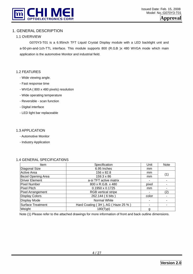
1.4 GENERAL SPECIFICATI0NS Item Specification Unit Note
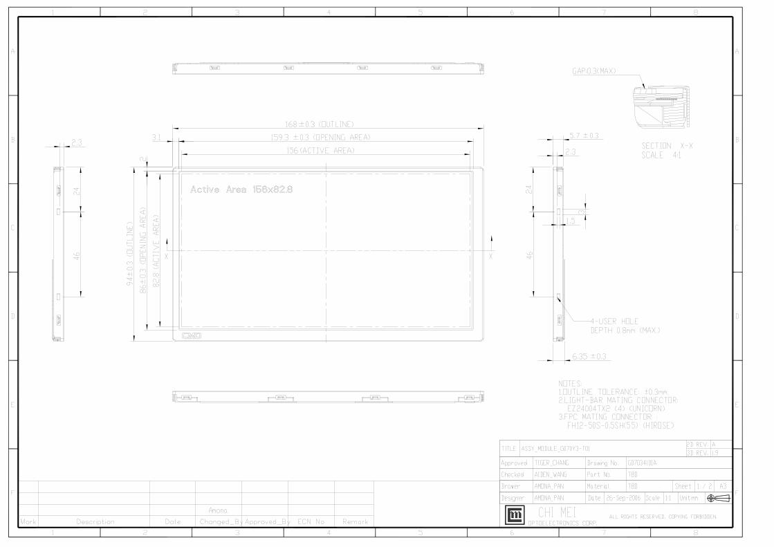
Diagonal Size 6.95 Inches mm Active Area 156 x 82.8 mm Bezel Opening Area 159.3 x 86 mm (1)
Driver Element a-si TFT active matrix - - Pixel Number 800 x R.G.B. x 480 pixel - Pixel Pitch 0.1950 x 0.1725 mm - Pixel Arrangement RGB vertical stripe - (2) Display Colors 262.144 ( 6 bits ) color - Display Mode Normal White - - Surface Treatment Hard Coating ( 3H ), AG ( Haze 25 % ) - - Weight 180(Typ) g
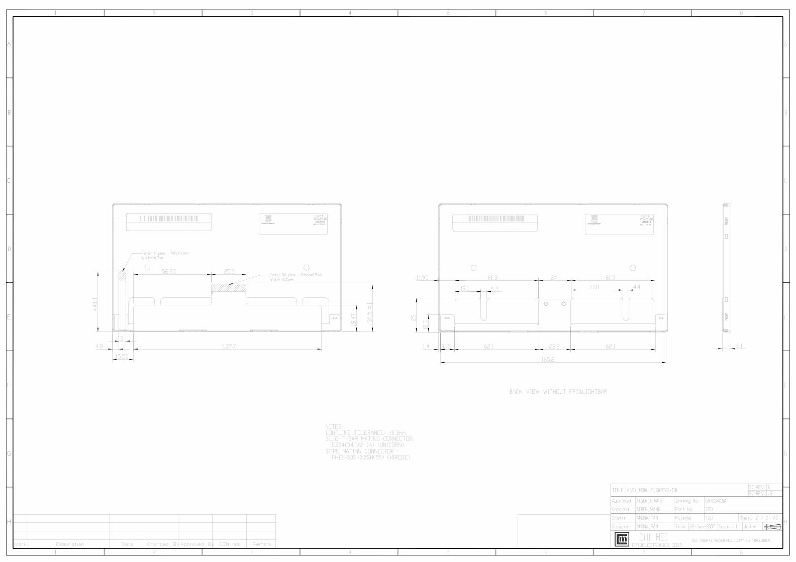
Note (1) Please refer to the attached drawings for more information of front and back outline dimensions.
4 / 27
Version 2.0
Issued Date: Feb. 15, 2008
Model No.:G070Y3-T01
Approval
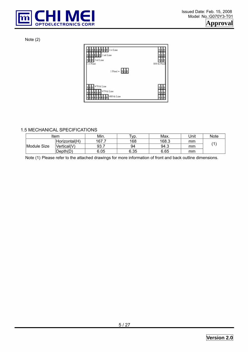
Note (2)
1.5 MECHANICAL SPECIFICATIONS Item Min. Typ. Max. Unit Note
Horizontal(H) 167.7 168 168.3 mm Vertical(V) 93.7 94 94.3 mm Module Size Depth(D) 6.05 6.35 6.65 mm
(1)
Note (1) Please refer to the attached drawings for more information of front and back outline dimensions.
5 / 27
Version 2.0

Issued Date: Feb. 15, 2008
Model No.:G070Y3-T01
Approval
2. ABSOLUTE MAXIMUM RATINGS 2.1 ABSOLUTE RATINGS OF ENVIRONMENT
No. Test Item Test Condition Note
1 High Temperature Storage 90, 240 hours
2 Low Temperature Storage -40, 240 hours
3 Thermal Shock Storage (-40, 0.5 hour) (85, 0.5 hour), 100 cycles
4 High Temperature Operating 85, 240 hours
5 Low Temperature Operating -30, 240 hours
6 High Temperature & High Humidity Operating 60, 90% RH, 240hours
(1) (2)
7 Shock (Non-Operating) 100G, 6ms, +/-XYZ 3 times (3)(5)
8 Vibration (Non-Operating) 3G, 10 to 200 Hz, sine wave (4)(5)
Note (1) There should be no condensation on the surface of panel during test.
Note (2) The temperature of panel display surface area should be 90 Max.
Note (3) 6ms, half sine wave, 3 times for +/-X, +/-Y, +/-Z.
Note (4) 3 directions: X, Y and Z axes, 60min per each direction; 6 cycles; sweep time = 5 minutes; peak
acceleration = 3G; frequency = 10 to 200 Hz; sine wave.
Note (5) At testing Vibration and Shock, the fixture in holding the module has to be hard and rigid enough
so that the module would not be twisted or bent by the fixture.
Note (6) In the standard conditions, there is no function failure issue occurred. All the cosmetic specification
is judged before the reliability test.
6 / 27
Version 2.0

Issued Date: Feb. 15, 2008
Model No.:G070Y3-T01
Approval
2.2 ELECTRICAL ABSOLUTE RATINGS 2.2.1 TFT LCD MODULE Ta = 25 ± 2 ºC
Value Parameter Symbol Min. Typ. Max. Unit Note
VCC -0.3 - 5 V - AVDD -0.3 - 13.5 V - VGH -0.3 - 42 V
Power Supply Voltage
VGL VGH-42 - 0.3 V - Digital Input Voltage VI -0.5 - Vcc+0.5 V (1)
V1~V5 0.4AVDD - AVDD+0.3 V - Gamma Supply Voltage
V6~V10 -0.3 - 0.6AVDD V -
Note (1) VI means all input logic signal.
2.2.2 BACKLIGHT UNIT Ta = 25 ± 2 ºC Value Item Symbol Min. Typ. Max. Unit Note
LED Light Bar Power Supply Voltage VL -45 - 31.5 V (1)
LED Light Bar Power Supply Current IL - - 90 mA (1)
Note (1) Permanent damage to the device may occur if maximum or minimum values are exceeded.
Function operation should be restricted to the conditions described under Normal Operating
Conditions.
7 / 27
Version 2.0
Issued Date: Feb. 15, 2008
Model No.:G070Y3-T01
Approval
3. ELECTRICAL CHARACTERISTICS 3.1 RECOMMENDED OPERATION CONDITION (GND = AVSS = 0V) Ta = 25 ± 2 ºC
Value Parameter Symbol Min. Typ. Max. Unit Note
VCC 3.0 3.3 3.6 V AVDD 10.29 10.5 10.71 V VGH 17.5 18 18.5 V
Power Supply Voltage
VGL -7.5 -7 -6.5 V V1~V5 0.4AVDD - AVDD+0.3 V (1) V6~V10 -0.3 - 0.6AVDD V (1) Input Signal Voltage VCOM - 4.035 - V
High Level VIH 0.7VCC - VCC V Digital Input Voltage
Low Level VIL 0 - 0.3VCC V
Note (1) Please refer to 11.1 application notes.
3.2 CURRENT CONSUMPTION (GND = AVSS =0V) Value Parameter Symbol Min. Typ. Max. Unit Note
Supply Current for Source/Gate Driver (Digital) ICC - 2.86 3.5 mA (1)
Supply Current for Source Driver (Analog) IDD - 21 25 mA (1)
Supply Current for Gate Driver (High Level) IGG - 0.13 0.2 mA (1)
Supply Current for Gate Driver (Low Level) IEE - 0.13 0.2 mA (1)
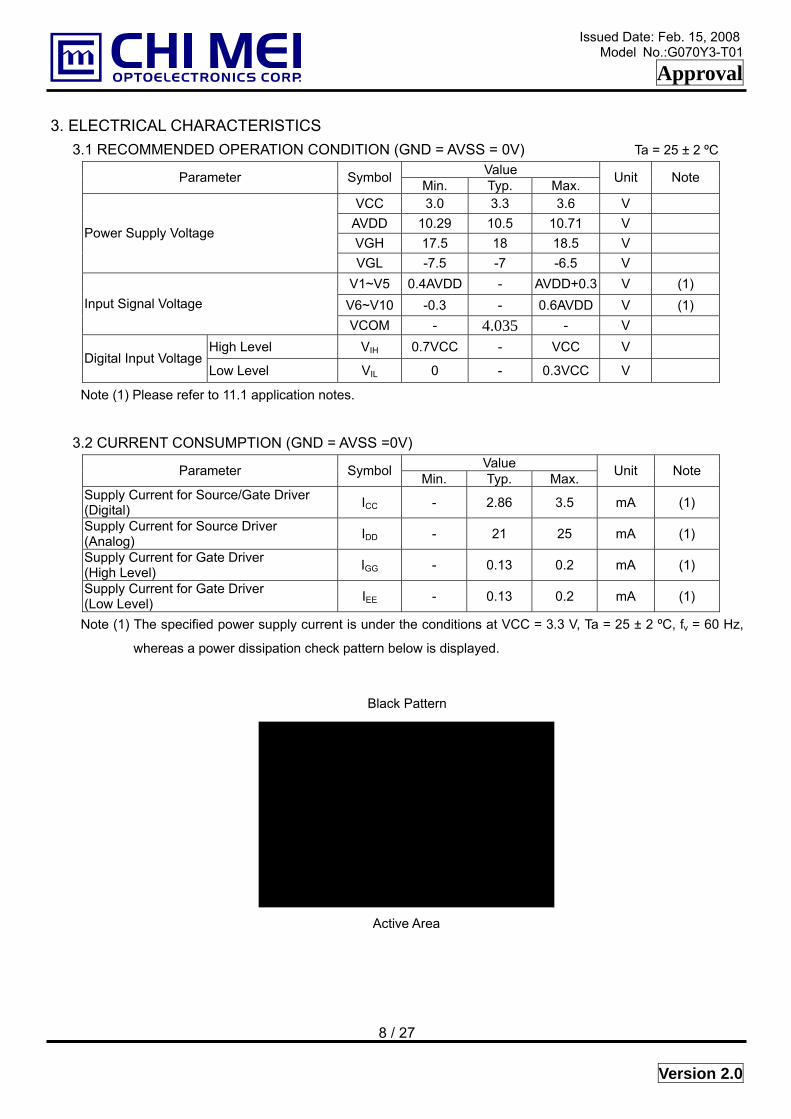
Note (1) The specified power supply current is under the conditions at VCC = 3.3 V, Ta = 25 ± 2 ºC, fv = 60 Hz,
whereas a power dissipation check pattern below is displayed.
Black Pattern
Active Area
8 / 27
Version 2.0
Issued Date: Feb. 15, 2008
Model No.:G070Y3-T01
Approval
3.3 BACKLIGHT UNIT Ta = 25 ± 2 ºC Value
Parameter Symbol Min. Typ. Max. Unit Note
LED Quantity 27 PCs (1)
LED Light Bar Power Supply Voltage VL 26.1 27.9 29.7 V
LED Light Bar Power Supply Current IL - 60 - mA (1),(2)
(Duty 100%)
Power Consumption PL - 1.674 - W (3), (Duty 100%)
LED Life Time LBL 10000 - - Hrs (4)
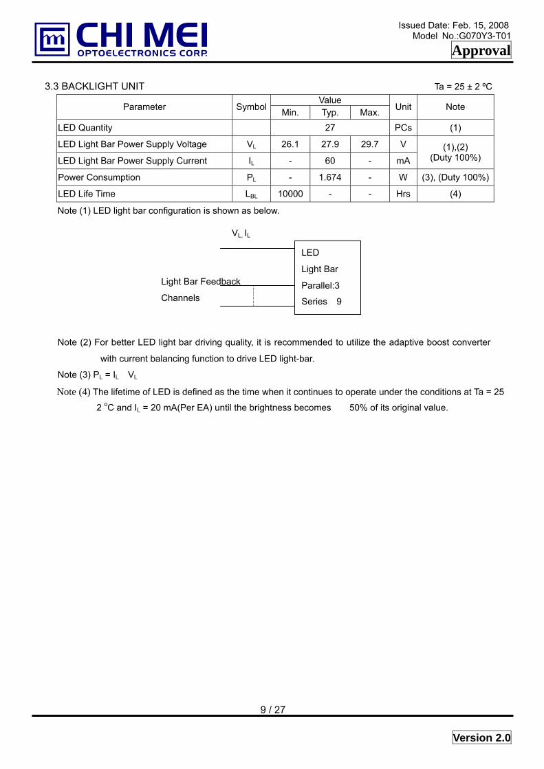
Note (1) LED light bar configuration is shown as below.
VL, IL
Light Bar Feedback
Channels
LED
Light Bar
Parallel:3
Series:9
Note (2) For better LED light bar driving quality, it is recommended to utilize the adaptive boost converter
with current balancing function to drive LED light-bar.
Note (3) PL = IL ×VL
Note (4) The lifetime of LED is defined as the time when it continues to operate under the conditions at Ta = 25
±2 oC and IL = 20 mA(Per EA) until the brightness becomes ≦ 50% of its original value.
9 / 27
Version 2.0
Issued Date: Feb. 15, 2008
Model No.:G070Y3-T01
Approval
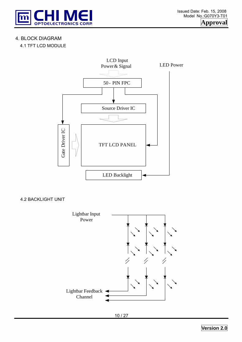
4. BLOCK DIAGRAM 4.1 TFT LCD MODULE
TFT LCD PANEL
Source Driver IC
50 - PIN FPC
LED Backlight
LED PowerG
ate
Driv
erIC
LCD Input Power & Signal
4.2 BACKLIGHT UNIT
Lightbar Input Power
Lightbar Feedback Channel
10 / 27
Version 2.0
Issued Date: Feb. 15, 2008
Model No.:G070Y3-T01
Approval
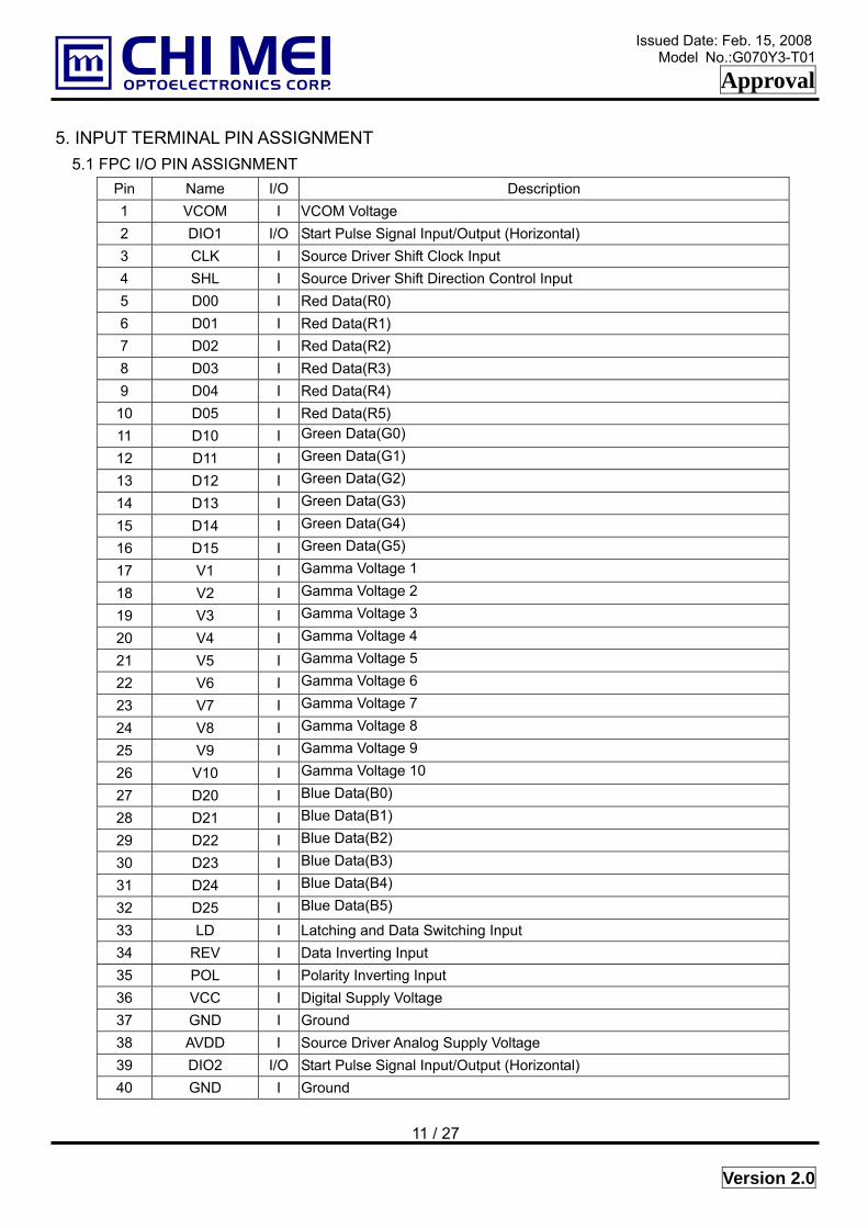
5. INPUT TERMINAL PIN ASSIGNMENT 5.1 FPC I/O PIN ASSIGNMENT
Pin Name I/O Description 1 VCOM I VCOM Voltage 2 DIO1 I/O Start Pulse Signal Input/Output (Horizontal) 3 CLK I Source Driver Shift Clock Input 4 SHL I Source Driver Shift Direction Control Input 5 D00 I Red Data(R0) 6 D01 I Red Data(R1) 7 D02 I Red Data(R2) 8 D03 I Red Data(R3) 9 D04 I Red Data(R4) 10 D05 I Red Data(R5) 11 D10 I Green Data(G0) 12 D11 I Green Data(G1) 13 D12 I Green Data(G2) 14 D13 I Green Data(G3) 15 D14 I Green Data(G4) 16 D15 I Green Data(G5) 17 V1 I Gamma Voltage 1 18 V2 I Gamma Voltage 2 19 V3 I Gamma Voltage 3 20 V4 I Gamma Voltage 4 21 V5 I Gamma Voltage 5 22 V6 I Gamma Voltage 6 23 V7 I Gamma Voltage 7 24 V8 I Gamma Voltage 8 25 V9 I Gamma Voltage 9 26 V10 I Gamma Voltage 10 27 D20 I Blue Data(B0) 28 D21 I Blue Data(B1) 29 D22 I Blue Data(B2) 30 D23 I Blue Data(B3) 31 D24 I Blue Data(B4) 32 D25 I Blue Data(B5) 33 LD I Latching and Data Switching Input 34 REV I Data Inverting Input 35 POL I Polarity Inverting Input 36 VCC I Digital Supply Voltage 37 GND I Ground 38 AVDD I Source Driver Analog Supply Voltage 39 DIO2 I/O Start Pulse Signal Input/Output (Horizontal) 40 GND I Ground
11 / 27
Version 2.0

Issued Date: Feb. 15, 2008
Model No.:G070Y3-T01
Approval
41 XAO I Output All-on Control 42 OE I Gate Driver Output Enable Control 43 UD_RL I Up/Down Scan Selection 44 CKV I Gate Driver Shift Clock input 45 STVU I/O Start Pulse Signal Input/Output (Vertical) 46 STVD I/O Start Pulse Signal Input/Output (Vertical) 47 VCC I Digital Supply Voltage 48 VGL I TFT Low Voltage 49 VGH I TFT High Voltage 50 GND I Ground
Note (1) User’s connector Part No: 089H50-000000-G2-C (Starconn) or equivalent
5.2 BACKLIGHT FPC PIN ASSIGNMENT
Pin Name I/O Description 1 VL I LED Light-bar Input Power 2 CH1 O Light-bar Feedback Channel 3 CH2 O Light-bar Feedback Channel 4 CH3 O Light-bar Feedback Channel
Note (1) User’s connector Part No: EZ24004G213 (UNE) or equivalent
12 / 27
Version 2.0
Issued Date: Feb. 15, 2008
Model No.:G070Y3-T01
Approval
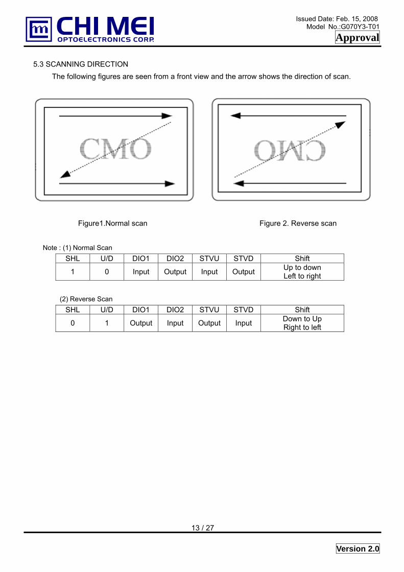
5.3 SCANNING DIRECTION The following figures are seen from a front view and the arrow shows the direction of scan.
Figure1.Normal scan Figure 2. Reverse scan
Note : (1) Normal Scan SHL U/D DIO1 DIO2 STVU STVD Shift
1 0 Input Output Input Output Up to down Left to right
(2) Reverse Scan SHL U/D DIO1 DIO2 STVU STVD Shift
0 1 Output Input Output Input Down to Up Right to left
13 / 27
Version 2.0
Issued Date: Feb. 15, 2008
Model No.:G070Y3-T01
Approval
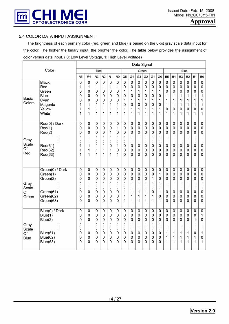
5.4 COLOR DATA INPUT ASSIGNMENT The brightness of each primary color (red, green and blue) is based on the 6-bit gray scale data input for
the color. The higher the binary input, the brighter the color. The table below provides the assignment of
color versus data input. ( 0: Low Level Voltage, 1: High Level Voltage)
Data Signal Red Green Blue Color
R5 R4 R3 R2 R1 R0 G5 G4 G3 G2 G1 G0 B5 B4 B3 B2 B1 B0
Basic Colors
Black Red Green Blue Cyan Magenta Yellow White
0 1 0 0 0 1 1 1
0 1 0 0 0 1 1 1
01000111
01000111
01000111
01000111
00101011
00101011
00101011
00101011
00101011
00101011
0 0 0 1 1 1 0 1
0 0 0 1 1 1 0 1
0 0 0 1 1 1 0 1
0 0 0 1 1 1 0 1
00011101
00011101
Gray Scale Of Red
Red(0) / Dark Red(1) Red(2)
: :
Red(61) Red(62) Red(63)
0 0 0 : : 1 1 1
0 0 0 : : 1 1 1
000::111
000::111
001::011
010::101
000::000
000::000
000::000
000::000
000::000
000::000
0 0 0 : : 0 0 0
0 0 0 : : 0 0 0
0 0 0 : : 0 0 0
0 0 0 : : 0 0 0
000::000
000::000
Gray Scale Of Green
Green(0) / Dark Green(1) Green(2)
: :
Green(61) Green(62) Green(63)
0 0 0 : : 0 0 0
0 0 0 : : 0 0 0
000::000
000::000
000::000
000::000
000::111
000::111
000::111
000::111
001::011
010::101
0 0 0 : : 0 0 0
0 0 0 : : 0 0 0
0 0 0 : : 0 0 0
0 0 0 : : 0 0 0
000::000
000::000
Gray Scale Of Blue
Blue(0) / Dark Blue(1) Blue(2)
: :
Blue(61) Blue(62) Blue(63)
0 0 0 : : 0 0 0
0 0 0 : : 0 0 0
000::000
000::000
000::000
000::000
000::000
000::000
000::000
000::000
000::000
000::000
0 0 0 : : 1 1 1
0 0 0 : : 1 1 1
0 0 0 : : 1 1 1
0 0 0 : : 1 1 1
001::011
010::101
14 / 27
Version 2.0

Issued Date: Feb. 15, 2008
Model No.:G070Y3-T01
Approval
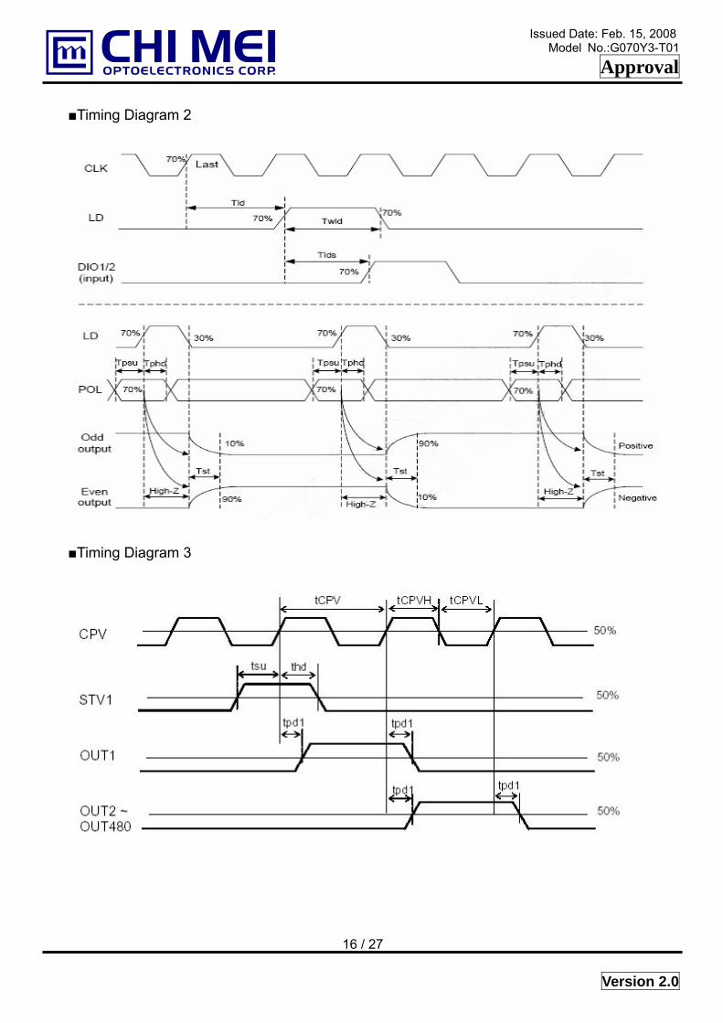
6. INTERFACE TIMING 6.1 AC ELECTRICAL CHARACTERISTICS (VCC = 3.3V, AVDD = 8.4V, AVSS = GND = 0V, Ta = 25)
Value Parameter Symbol Min. Typ. Max. Unit Condition
CLK frequency Fclk - 40 45 MHz - CLK Pulse width Tcw 40% - 60% TCLK - Data setup time Tsu 4 - - ns D00~D25, REV and DIO1/2 to CLKData hold time Thd 2 - - ns D00~D25, REV and DIO1/2 to CLKPropagation delay of DIO2/1 Tphl 6 10 15 ns CL = 25pF (Output) Time that the last data to LD Tld 1 - - TCLK - Pulse width of LD Twld 2 - - TCLK - Time that LD to DIO1/2 Tlds 5 - - TCLK - POL setup time Tpsu 6 - - ns POL to LD POL hold time Tphd 6 - - ns POL to LD
Output stable time Tst - - 12 us 10% or 90% target voltage, CL = 60pF, R = 2KΩ
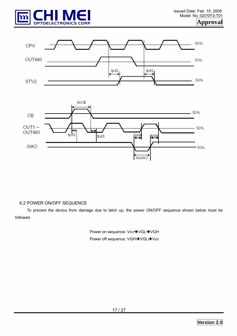
CKV period tCPV 5 - - us - CKV pulse width tCPVH,tCPVL 2.5 - - us 50% duty cycle OE pulse width tWOE 1 - - us - XAO pulse width tWXAO 10 - - us Data setup time tsu 700 - - ns - Data hold time thd 700 - - ns - Output delay time (1) tPd1 - - 1000 ns CL = 300pF Output delay time (2) tPd2 - - 800 ns CL = 30pF Output delay time (3) tPd3 - - 800 ns CL = 300pF Output delay time (4) tPd4 - - 10000 ns CL = 300pF
Timing Diagram 1
15 / 27
Version 2.0
Issued Date: Feb. 15, 2008
Model No.:G070Y3-T01
Approval
Timing Diagram 2
Timing Diagram 3
16 / 27
Version 2.0
Issued Date: Feb. 15, 2008
Model No.:G070Y3-T01
Approval
6.2 POWER ON/OFF SEQUENCE To prevent the device from damage due to latch up, the power ON/OFF sequence shown below must be
followed.
Power on sequence: Vcc VGL VGH
Power off sequence: VGH VGL Vcc
17 / 27
Version 2.0
Issued Date: Feb. 15, 2008
Model No.:G070Y3-T01
Approval
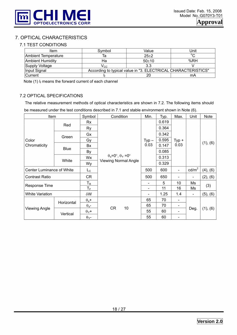
7. OPTICAL CHARACTERISTICS 7.1 TEST CONDITIONS
Item Symbol Value Unit Ambient Temperature Ta 25±2 oC Ambient Humidity Ha 50±10 %RH Supply Voltage VCC 3.3 V Input Signal According to typical value in "3. ELECTRICAL CHARACTERISTICS" Current If 20 mA
Note (1) If means the forward current of each channel
7.2 OPTICAL SPECIFICATIONS
The relative measurement methods of optical characteristics are shown in 7.2. The following items should
be measured under the test conditions described in 7.1 and stable environment shown in Note (6). Item Symbol Condition Min. Typ. Max. Unit Note
Rx 0.619 Red
Ry 0.364 Gx 0.342
Green Gy 0.595 Bx 0.147
Blue By 0.085 Wx 0.313
Color Chromaticity
White Wy
Typ – 0.03
0.329
Typ + 0.03 (1), (6)
Center Luminance of White LC 500 600 - cd/m2 (4), (6)
Contrast Ratio CR 500 650 - - (2), (6)TR - 5 10 Ms Response Time TF - 11 16 Ms
(3)
White Variation δW
θx=0°, θY =0° Viewing Normal Angle
- 1.25 1.4 - (5), (6)θx+ 65 70 - Horizontal θx- 65 70 - θY+ 55 60 -
Viewing Angle Vertical
θY-
CR ≧ 10
55 60 -
Deg. (1), (6)
18 / 27
Version 2.0
Issued Date: Feb. 15, 2008
Model No.:G070Y3-T01
Approval
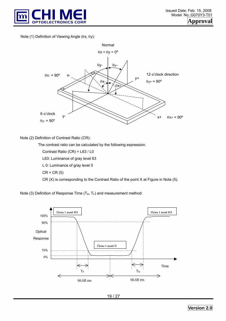
Note (1) Definition of Viewing Angle (θx, θy):
θX- = 90º
θX+ = 90º
Normal
θx = θy = 0º
x+ y-
y+x-
θy+ θy-
θx+ θx−
6 o’clock
θy- = 90º
12 o’clock direction
θy+ = 90º
Note (2) Definition of Contrast Ratio (CR):
The contrast ratio can be calculated by the following expression.
Contrast Ratio (CR) = L63 / L0
L63: Luminance of gray level 63
L 0: Luminance of gray level 0
CR = CR (5)
CR (X) is corresponding to the Contrast Ratio of the point X at Figure in Note (5).
Note (3) Definition of Response Time (TR, TF) and measurement method:
ss
TF TR
Time
Gray Level 63
Gray Level 0
Gray Level 63100%
90%
10%
0%
Optical
Response
66.68 m19 / 27
66.68 m
Version 2.0
Issued Date: Feb. 15, 2008
Model No.:G070Y3-T01
Approval
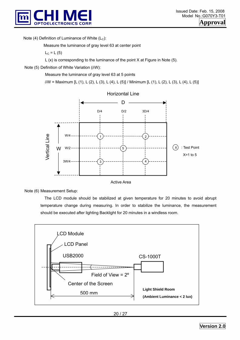
Note (4) Definition of Luminance of White (LC):
Measure the luminance of gray level 63 at center point LC = L (5)
L (x) is corresponding to the luminance of the point X at Figure in Note (5).
Note (5) Definition of White Variation (δW):
Measure the luminance of gray level 63 at 5 points
δW = Maximum [L (1), L (2), L (3), L (4), L (5)] / Minimum [L (1), L (2), L (3), L (4), L (5)]
Horizontal Line
X
3W/4
W/2
W/4
3D/4D/2D/4
43
21
5 : Test Point
X=1 to 5 W
D
Verti
cal L
ine
Active Area
Note (6) Measurement Setup:
The LCD module should be stabilized at given temperature for 20 minutes to avoid abrupt
temperature change during measuring. In order to stabilize the luminance, the measurement
should be executed after lighting Backlight for 20 minutes in a windless room.
USB2000
Light Shield Room
(Ambient Luminance < 2 lux)
Center of the Screen
LCD Panel
LCD Module
500 mm
Field of View = 2º
CS-1000T
20 / 27
Version 2.0

Issued Date: Feb. 15, 2008
Model No.:G070Y3-T01
Approval
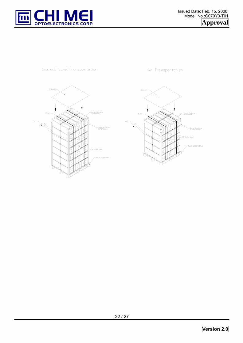
8. PACKAGING
21 / 27
Version 2.0
Issued Date: Feb. 15, 2008
Model No.:G070Y3-T01
Approval
22 / 27
Version 2.0
Issued Date: Feb. 15, 2008
Model No.:G070Y3-T01
Approval
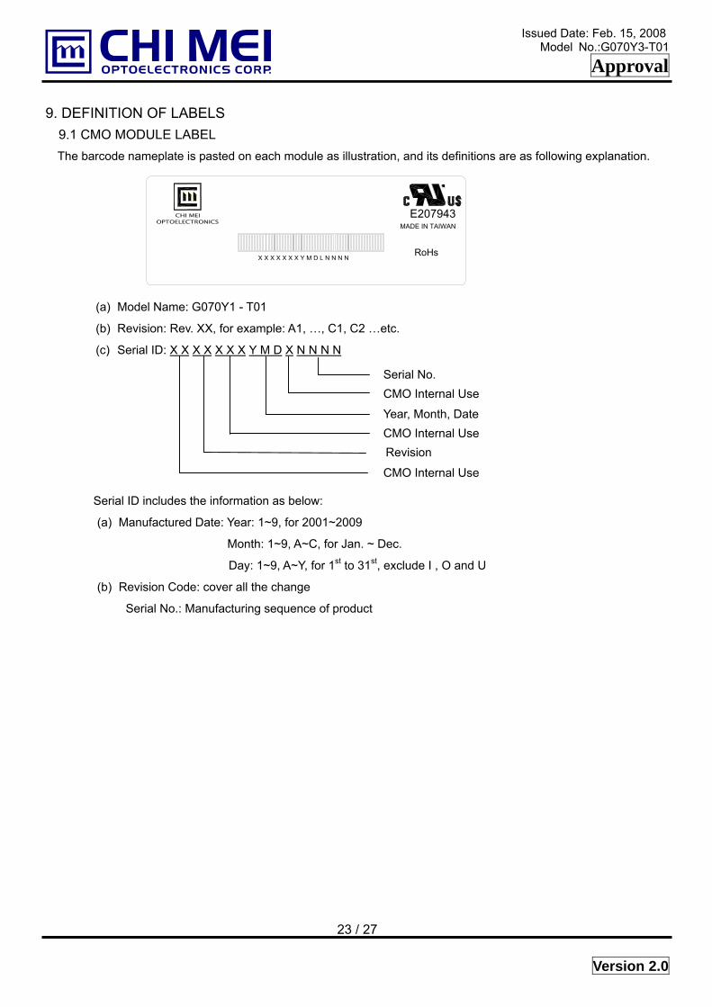
9. DEFINITION OF LABELS 9.1 CMO MODULE LABEL The barcode nameplate is pasted on each module as illustration, and its definitions are as following explanation.
MADE IN TAIWAN943
X X X X X X Y M D L N N N N
P 1 3 5 4 4 8 - 0 1
A
N141X5 - L03 Rev.XX
C
01 s
(a) Model Name: G070Y1 - T01
(b) Revision: Rev. XX, for examp
(c) Serial ID: X X X X X X X Y M
Serial ID includes the information
(a) Manufactured Date: Year: 1~
Month:
Day: 1~
(b) Revision Code: cover all the
Serial No.: Manufacturing s
X
E207G070Y3 -T01 Rev. XX
le: A1, …, C1, C2 …etc.
D X N N N N
SeriaCMO
Year,CMORev
CMO
as below:
9, for 2001~2009
1~9, A~C, for Jan. ~ Dec.
9, A~Y, for 1st to 31st, exclu
change
equence of product
23 / 27
RoH
l No. Internal Use Month, Date Internal Use
ision
Internal Use
de I , O and U
Version 2.0
Issued Date: Feb. 15, 2008
Model No.:G070Y3-T01
Approval
10. PRECAUTIONS 10.1 ASSEMBLY AND HANDLING PRECAUTIONS
(1) Do not apply rough force such as bending or twisting to the module during assembly.
(2) To assemble or install module into user’s system can be only in clean working areas. The dust and oil
may cause electrical short or worsen the polarizer.
(3) It’s not permitted to have pressure or impulse on the module because the LCD panel and Backlight will
be damaged.
(4) Always follow the correct power sequence when LCD module is connecting and operating. This can
prevent damage to the CMOS LSI chips during latch-up.
(5) Do not pull the I/F connector in or out while the module is operating.
(6) Do not disassemble the module.
(7) Use a soft dry cloth without chemicals for cleaning, because the surface of polarizer is very soft and
easily scratched.
(8) It is dangerous that moisture come into or contacted the LCD module, because moisture may damage
LCD module when it is operating.
(9) High temperature or humidity may reduce the performance of module. Please store LCD module within
the specified storage conditions.
(10) When ambient temperature is lower than 10ºC may reduce the display quality. For example, the
response time will become slowly, and the starting voltage of CCFL will be higher than room
temperature.
10.2 SAFETY PRECAUTIONS (1) The startup voltage of Backlight is approximately 1000 Volts. It may cause electrical shock while
assembling with inverter. Do not disassemble the module or insert anything into the Backlight unit.
(2) If the liquid crystal material leaks from the panel, it should be kept away from the eyes or mouth. In
case of contact with hands, skin or clothes, it has to be washed away thoroughly with soap.
(3) After the module’s end of life, it is not harmful in case of normal operation and storage.
24 / 27
Version 2.0
Issued Date: Feb. 15, 2008
Model No.:G070Y3-T01
Approval
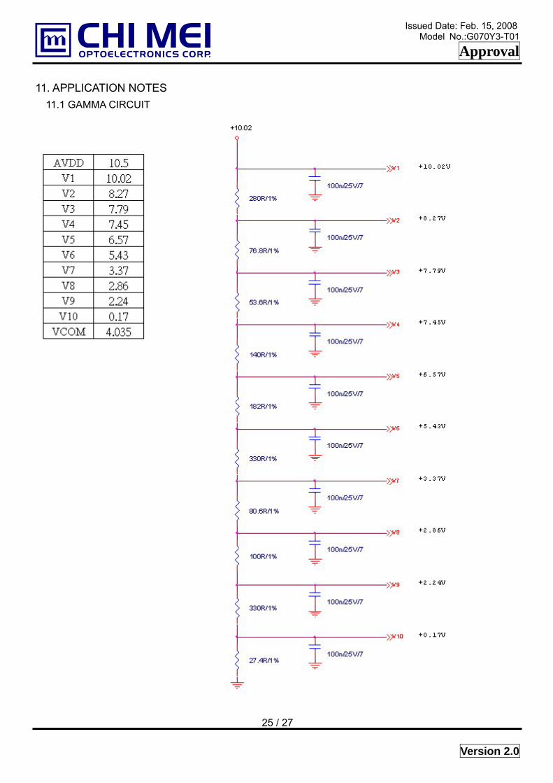
11. APPLICATION NOTES 11.1 GAMMA CIRCUIT
25 / 27
Version 2.0