mmc-based vsc-hvdc link
TRANSCRIPT

energies
Article
Interaction Assessment and Stability Analysis of theMMC-Based VSC-HVDC Link
Saman Dadjo Tavakoli * , Eduardo Prieto-Araujo , Enric Sánchez-Sánchezand Oriol Gomis-Bellmunt
CITCEA-UPC, Department of Electrical Engineering, Universitat Politècnica de Catalunya, Av. Diagonal 647,08028 Barcelona, Spain; [email protected] (E.P.-A.); [email protected] (E.S.-S.);[email protected] (O.G.-B.)* Correspondence: [email protected]
Received: 28 February 2020; Accepted: 17 April 2020; Published: 21 April 2020
Abstract: This paper investigates the dynamic behavior of a modular multi-level converter(MMC)-based HVDC link. An overall state-space model is developed to identify the system criticalmodes, considering the dynamics of the master MMC and slave MMC, their control systems, and theHVDC cable. Complementary to the state-space model, an impedance-based model is also derivedto obtain the minimum phase margin (PM) of the system. In addition, a relative gain array (RGA)analysis is conducted to quantify the level of interactions among the control systems of master andslave MMCs and their impacts on stability. Finally, with the help of the results obtained from thesystem analysis (eigenvalue, phase margin, sensitivity, and RGA), the system dynamic performanceis improved.
Keywords: HVDC; MMC; mutual interactions; small-signal analysis; state-space model
1. Introduction
Modular multi-level converter (MMC) has emerged as the preferred choice for voltage sourceconverter (VSC)-based HVDC systems mainly due to low losses, low harmonic distortion, scalability,and redundancy [1,2]. However, the control design for an MMC is more challenging as compared toa conventional two-level VSC, which is due to the extra control actions required for the regulation ofthe internal energy balances. The different control schemes proposed in the literature can be classifiedas follows. First, the non-energy-based control method (also known as uncompensated modulation)in which the internal energy of the MMC is not explicitly regulated [3–7]. This control approach isasymptotically stable but the transient response of MMC depends on the converter impedance ratherthan being dictated by the control actions, which leads to slow and undesirable dynamics [8]. Moreover,it imposes parasitic circulating current components that require additional current control loops toattenuate them [3]. An alternative approach is to implement an energy-based method, also known ascompensated modulation or closed-loop modulation [8–11]. This control method does not generateparasitic voltage components, but energy controllers are required to ensure an asymptotically stablesystem [12].
Considering the energy-based method, several control loops are required to achieve certainobjectives. Commonly, these control loops are structured to form a cascade control in which the outercontrol loops generate references for the inner loops. The outer control loops involve the energycontrol, DC voltage control (in case of master MMC), and active power control (in case of slaveMMC), which provide references for the grid current control and the additive current (also known ascirculating current) control [8]. The design and tuning of these control loops are challenging since thereis a strong coupling among them [13,14]. For instance, a change in the energy reference of the slave
Energies 2020, 13, 2075; doi:10.3390/en13082075 www.mdpi.com/journal/energies
Energies 2020, 13, 2075 2 of 19
MMC would cause a transient in the DC voltage of the master MMC, and vice versa. These interactionscan reduce the stability margin of the system and even lead to instability [15].
Hence, in a system with strong coupling among control variables, the design and tuning ofa control loop needs to be conducted such that the overall stability margin of the entire system ismaintained and an elevated level of interactions among control loops is avoided [16]. In fact, if the levelof interactions among control loops is not considered during the design of a control loop, the attemptsto obtain a locally optimal control loop with fast response and suppressed over/undershoot may forcethe entire system to operate in a high interaction conditions with reduced stability margin.
In order to evaluate the system stability and the level of the interactions among control loops,a linear model of the MMC-based HVDC system is needed, which can be derived using one of thefollowing modeling approaches:
• State-space modeling based on dq transformation [8,11,14,17]: in this modelling approach,the electrical circuit equations of an MMC are commonly transformed to dq-frame and expressedin state-space equations. These equations are interconnected to the state-space equations ofthe control loops based on the similar input/output signals in order to formulate an overalllinear model of an MMC. Although this modeling approach offers a high level of modularity,the inclusion of the circulating current harmonics in the modeling is challenging [11].
• State-space modeling based on the dynamic phasor [18–22]: this modeling approach is also basedon the state-space modeling techniques, but the system is in abc-frame. It is a suitable modelingmethod for studying the impact of harmonics on the system stability [18].
• Impedance-based modeling [23–25]: in this modeling approach, the impedance of the MMC atthe AC and DC sides are analytically computed. A major advantage of this method is the abilityto judge the system stability margin [23].
Once the linear model of an MMC is derived using one of the above-mentioned methods,the model should be extended to include the dynamics of other system components, such as theHVDC cable, to formulate the overall linear model of the system suitable for stability assessment andinteraction analysis. Several studies have only focused on the linear model of a single MMC and,to some extent, ignored the dynamics of either DC or AC networks. In [26], a simplified model ofan MMC is developed aiming for adopting a sliding mode control in abc-frame, which simplifies thecomplexity of the dq-frame transformation related to the MMC circulating current. The linear modelof an MMC is derived for the system stability assessment in [6], and the control system is designedbased on the linear model [27]. However, the linear model does not include the dynamics of the slaveMMC. In [14], a linear state-space model of an HVDC system is derived to analyze the system transientresponse, suggesting alternative controllers to improve the converter dynamic behavior. However,it does not provide information on the system phase margin (PM) and the interactions among thecontrol loops are neither addressed.
In this paper, a procedure is suggested to include two key global aspects of an MMC-based HVDClink in the control system design: (1) the overall PM of the system, and (2) the level of interactionsamong the control loops. Two linear models that accurately capture the dynamics of the master andslave MMCs, their control systems, and the HVDC cable are developed to identify the control loopwith the most adversary impact on the system overall dynamics, and design this control loop withthe consideration of the overall performance of the system, rather than only focusing on the localperformance requirements such as the maximum over/undershoot.
The rest of the paper is organized as follows. In Section 2, the configuration of the HVDC link andthe control system of MMC are described. In Section 3, the state-space equations of the complete systemare derived and linearized, which are later used in Section 4 to build an overall state-space model of thesystem. In Section 5, complementary to the overall state-space model, an impedance-based model isderived to provide additional insight into the dynamic behavior of the HVDC link. Once the two linearmodels are derived, the system stability is studied and the critical modes are identified through

Energies 2020, 13, 2075 3 of 19
an eigenvalue and participation factors analysis in Section 6. Moreover, the system minimum PM iscalculated through an impedance-based analysis using the Nyquist plot, and the level of interactionsamong control loops is studied using a frequency-dependent relative gain array (RGA) analysis. Finally,in Section 7, based on the results achieved from the system analyses, the stability of the system isimproved by tuning the DC voltage control loop.
2. System Description
A typical HVDC link between two AC networks is shown in Figure 1. In such configuration,the master MMC regulates DC voltage while the slave MMC controls active power exchange [27].Either AC voltage or reactive power can be regulated at both ends.
AC network 1
HVDC cable
AC network 2Master Slave
Vdc control P control
Figure 1. Multi-level converter (MMC)-based HVDC link.
The average-value model of the MMC structure connected to an AC network is presented inFigure 2. Compared to the detailed model, the IGBTs of submodules are not explicitly modeled and theMMC dynamics are represented by controlled voltage and current sources [2,28,29]. In [30], it has beenshown that the average-value model accurately replicates the dynamic performance of the detailedmodel, and it is significantly more efficient for simulation time steps.
Arm
nvgb
vga
vgcc0
Vudc
Phasereactor
AC networkequivalent
Rg Lg sR Ls
Rg Lg sR Ls
sR Ls
+ub
ua
ucc
isa
SMu1a
SMu2a
SMuma
iua
vua
Ra
La
ila
SM
SM
SM
iub
v ub
Ra
La
u1b
u2b
umb
vub
SM
SM
SM
iuc
Ra
La
vuc
u1c
u2c
umc
ilcil
b
SMl1a
SMl2a
SMlma
vla
SM
SM
SM
l1b
l2b
lmb
vlb
SM
SM
SM
vlc
l1c
l2c
lmc
Rg Lg
isb
isc
Ra
La
Ra
La
Ra
La
+
+
Vldc
Leg
Armreactor
+
Submodule
CSM
+-
Ceqvla
Arm Averaged Model(AAM)
+
Cv uaC v u
cC
v lbCv l
aC v l
cC
v laC
i laC
Figure 2. Average-value model (AVM) of MMC connected to an AC network.

Energies 2020, 13, 2075 4 of 19
Referring to Figure 2, the MMC consists of six arms, each of them contains Narm half-bridgesubmodules with a capacitance CSM and an arm reactor connected in series. The three legs,corresponding to three phases, can be divided into upper and lower arms. The six arms synthesizethe required AC and DC voltages to achieve the desired power exchange between the AC and DCsides. The control system of both MMCs is based on the energy-controlled approach and presentedin Figure 3. The grid side current controller tracks the current references sent by the outer control loop.In the case of the master MMC, the DC voltage outer control loop provides the q-axis current reference,whereas, in the slave MMC, it is provided by the active power control loop. In both cases, the d-axiscurrent reference is given by the reactive power control loop. In addition, the energy balancing andtotal energy control send the circulating current reference for the inner current controller. Furthermore,a Phase Locked Loop (PLL) tracks the AC voltage in the point of connection with the AC network.The outputs of both the current control systems (grid side and circulating) are used to generate thesix-arm voltages. Finally, the modulation and cell-balancing algorithm are responsible for generatingthe required voltage through communication with the submodule switches.
Qac*
vdiffβ
vdiff0
vdiffα
vsumβ
vsum0
vsumα
*Pa b
Pa c*
Pt*
+
vla
vlb
vlc
vuc
vua
vub
isumβ isum
0isumα
va vb vCuc
Wa b
Wa c
Wt
Armenergy
calculation
isumαdc*
isumβdc*
isum0dc*
Vu
-
Grid sidecurrentcontrol
Additivecurrentcontrol
Energycontrol
*Wa bWa c*Wt
*
va vb vc
referenceReactive poweris
d*
isq*
Armsvoltage
calculation
uqd isqd
uabcuqd
θ
Active power control Pac*
DC voltage control
Additivecurrent
reference
+Vl
Phaselockedloop
Inner loop
Outer loop
Reference calculation
Vtdc*
Wu l
Wu l
Wu la
b
c
P
P
P
u l
u l
u la
b
c
*
*
*
*Wu l
a *Wu l
b *Wu l
c
isumβdc isum
0dcisumαdc
isumα*
isumβ*
isum0*
Pac*Vt
dc*
CuCu
ClClCl
andmodulation
vabcCu
vabcCl
dc dc
Figure 3. MMC energy-based control system.
3. System Modeling
In this section, a non-linear model of an MMC-based HVDC link is derived. This non-linearmodel is then linearized to obtain an overall linear model of the system. More details and explanationsare provided in [8].
3.1. Modular Multilevel Converter (MMC)
Figure 2 shows the MMC average model electrical circuit. The equations per phase are
Vdcu − vj
u − vjg − vn =
Raiju + La
diju
dt+ (Rs + Rg)i
js + (Ls + Lg)
dijs
dt(1)
−Vdcl + vj
l − vjg − vn =
− Raijl − La
dijl
dt+ (Rs + Rg)i
js + (Ls + Lg)
dijs
dt, (2)

Energies 2020, 13, 2075 5 of 19
where, Ra and La are arm resistance and inductance, Rs and Ls are AC grid filter resistance andinductance, Vdc
u and Vdcl are upper and lower voltages of the HVDC link. The AC grid current and
Thévenin voltage are, respectively, ijs and vj
g, while the voltages applied by the upper and lower arms
are vju and vj
l . The currents flowing through the upper and lower arms are indicated by iju and ij
l ,respectively.
The following variable change is common in MMC modeling [8]
vjdiff ,
12(− vj
u + vjl)
vjsum , vj
u + vjl
ijsum ,
12(iju + ij
l)
R , Rs + Rg +Ra
2L , Ls + Lg +
La
2
vju = −vj
diff +12
vjsum
vjl = vj
diff +12
vjsum
iju =
12
ijs + ij
sum
ijl = −
12
ijs + ij
sum
, (3)
where vjdiff is the differential voltage, approximately equal to the AC voltage at the point of connection
and ijsum is the additive current circulating from the upper to the lower arm of the leg j (j = a, b, c).
The additive voltage is indicated by vjsum and it is approximately equal to the sum of the DC poles
voltages. Then, adding and subtracting (1) and (2) and using the variable change given by (3) wouldlead to
12(Vdc
u −Vdcl)+ vj
diff − vjg − vn = Rij
s + Ldij
sdt
(4)
vjsum −
(Vdc
u + Vdcl)= −2Raij
sum − 2Ladij
sum
dt. (5)
Equations (4) and (5) are decoupled and only contain a single derivative term (ijs and ij
sum).Hence, they are suitable for state-space representation. The current ij
sum contains AC and DC termswhich impact the performance of the control system in various aspects. The DC term of ij
sum can betransformed into (αβ0) frame. The zero component is used for the control of the power flow into theDC grid, while the (αβ) components regulate the internal power exchange between legs. The AC termof ij
sum contains (+− 0) sequences. The zero sequence is controlled to zero, avoiding AC distortion inthe DC grid, whereas (+−) sequences can be used to regulate the internal power exchange betweenupper and lower arms of each leg. A comprehensive discussion can be found in [8].
Since ijsum contains AC terms with various frequencies, the transformation into (qd) frame becomes
complicated. However, these components are relevant for the DC pole imbalances studies [31].Considering only the DC term of ij
sum, the system becomes suitable for linearization. Using thefollowing definitions
Vdcoff ,
12(Vdc
u −Vdcl), Vdc
t , Vdcu + Vdc
l (6)
combined with (4) and (5), yields
vabcdiff − vabc
g +(Vdc
OFF − vn)(1 1 1)T = RI3iabc
s + LI3diabc
sdt
(7)
vαβ0dcsum −Vdc
t (0 0 1)T = −2RaI3iαβ0dcsum − 2LaI3
diαβ0dcsum
dt, (8)
where In is an identity matrix of order n. Combining (7) and (8) and considering only the DC term ofijsum, three linear state-space equations can be derived. The three state variables are ∆iq
s , ∆ids , and ∆i0dc
sum.

Energies 2020, 13, 2075 6 of 19
3.2. MMC Control
The detailed control system of master/slave MMC is presented in Figure 3. The control systemhas two main parts detailed above; the grid control and the energy control parts. This control systemis used in the nonlinear model of MMCs. However, for the small-signal analysis, it is assumed that theinternal energy balance is properly performed; so only a total energy control is required to regulate thezero component of ij
sum [32]. Based on this assumption, the linear model derivation can be simplifiedwhile maintaining a high level of accuracy. More details and information regarding the linearizationof the PLL and active power equation are provided in [33]. The control system with total energycontrol is presented in Figure 4. The master MMC has two main closed-loop cascaded control systems,which are DC voltage control Vdc
t and total energy control Wt1 (which generates the reference for theinner additive current (i0dc∗
sum ) control loop). In the case of slave MMC, it has an active power controlloop P2 and again a total energy control. For the sake of clarity, the master and slave MMCs areindicated as MMC 1 and MMC 2, respectively.
+
-
-+
+
-
+
uq
ud
DC voltage loop
++-
vdiffqd
*
*
+
Wt*
Wt
-
++
isum0dc*
-
isumdc
Pcalcisqd
uqd
isqd
isd
isq
isq
isd
ωLc
ωLc
Pt*
Energy loopAdditive current loop
Grid current loop
0
-+
Vtdc
+
2U
√
PI is PI Vdc
PI WtPI isum
PI is*Q
Vtdc*
VtdcVt
dc*
N
-
+
+
+
ac
vsum0dc
I dc*
+1
3Vtdc*
+
2U
√
N3√
3√
Figure 4. The control system of the master MMC in linear model.
3.3. HVDC Cable
The HVDC cable is modeled using a lumped parameters vector fitting method introduced in [34].In the present case, as it is shown in Figure 5, a five-section model is considered to account for thehyperbolic correction factors, which makes the model more accurate, in particular for long cables.
C
R1 1-2,1 L1
R2 L2
R3 L3
G22
Vt1
CG22
dc
CG
i
1-2,2 i
1-2,3 i
i1 i2v1,2+
Vt2dc
AC Network 1 AC Network 2
Sec.1 Sec.5Vt1dc
i1
Vt2dc
i2
Figure 5. HVDC cable model based on lumped parameters vector fitting method.

Energies 2020, 13, 2075 7 of 19
4. System Overall State-Space Model
The purpose of this section is to formulate a linear state-space model with the desiredinput/output pairs, which is suitable for the eigenvalue analysis and the control interactions studies.To obtain this model, the individual state-space models of the master and slave MMCs (MMC 1 andMMC 2), their corresponding control systems, and the HVDC cable are interconnected together basedon the similar input/output signal names. The overall state-space model of the HVDC link is given by
∆x = A∆x + B∆z, ∆y = C∆x + D∆z, (9)
where ∆x is a state vector including 43 states of the entire HVDC link, ∆z is a vector of the system inputs,and ∆y is a vector of desired outputs. The overall model has 43 state variables and the input/outputvectors are selected as follows
∆z =(∆Vdc∗
t , ∆P∗2 , ∆W∗t1, ∆W∗t2, ∆vqdg1, ∆vqd
g2, ∆Q∗1 , ∆Q∗2)
∆y =(∆Vdc
t , ∆P2, ∆Wt1, ∆Wt2). (10)
The overall linear model of the HVDC link based on the state-space equations is presented inFigure 6. As mentioned earlier, in the linear model, only the total energy control loop of MMCs isconsidered, assuming that the energy balance between the legs and upper and lower arms is performedin an adequate manner.
The validation of the linear model is performed through a time domain simulation (see Figure 3),in which a detailed energy-based nonlinear model of the MMC with the complete control systemis used [8]. First, the active power (P2) is increased by 20%, then reduced again by similar value.The responses related to various variables in MMC 1 are shown in Figure 7, which confirms theaccuracy of the linear model. The parameters of the system can be found in Tables A1 and A2 ofthe Appendix A.
Δuqdc
Δeθ
Tcqd
ΔiqdcsTc
qd Δvqdc Tcqd-1
Δvqd
ΔisΔuqd
ΔeθΔeθΔiqds
MMC 1
ΔV1
Δiqds
PLL
Δuqd
Δisum0dc
diff diff
AC sidecurrent
loop
Circ.current
loop
ΔW
ΔVtdc*
Δvsum0dc
Energyloop
Δud
Δisum0dc*
q*
ΔvqdgΔWt*
Δid*s
Δuqdc
Δeθ
Tcqd
ΔiqdcsTcqd Δvqdc
Tcqd-1
Δvqd
ΔisΔuqdΔeθΔeθ
Δiqds
MMC 2
ΔP
ΔV2
Δiqds
PLL
Δuqd
Δisum0dc
diff diffAC sidecurrent
loop
Circ.current
loop
Δ
*
Δvsum0dc
Δud
Δisum0dc*
q*
ΔvqdgΔWt*
Δid*s
ΔV1
ΔV2
ΔV1
ΔV1
DC voltage loop
HVDC Cable,
Active power loop
ΔV2
Δiqdcs Δuqdc,
Δi2
Δi1
Δi1 Δi2,
Energyloop
t
Wt
ΔWt
ΔWt
ΔQ*( )
ΔQ*( )
Master
Slave
Figure 6. Linear model of the HVDC link with cascaded total energy control loop.

Energies 2020, 13, 2075 8 of 19
0.4 0.45 0.5 0.55 0.6 0.65 0.7 0.75
Time [s]
480
500
520
540
560
580
0.4 0.45 0.5 0.55 0.6 0.65 0.7 0.75
Time [s]
620
640
660
0.4 0.45 0.5 0.55 0.6 0.65 0.7 0.75
Time [s]
1250
1300
1350
1400
1450
0.4 0.45 0.5 0.55 0.6 0.65 0.7 0.75
Time [s]
24.54
24.56
24.58
24.60
non-linear model
linear modelP1 [
MW
]V
t [k
V]
i s
[A]
Wt [
MJ]
dc
q
Figure 7. Comparison between the transient responses of the linear and non-linear models.
The multi-input multi-output (MIMO) model presented in Figure 8 is built from the linear model.The complete state-space model is transformed into the Laplace domain and the system transferfunction matrix, Tsys(s), relating different input-output variables, is derived.
K=1 K=0.7
K=0.5 K=0.1
K=0.01
Unstable
nonlinear model linear model
0.38 0.42 0.46 0.5 0.54
500
520
540
P1
[MW
]
Time [s]0.38 0.42 0.46 0.5 0.54
640
650
660
V
t [k
V]
dc
Time [s]
0.38 0.42 0.46 0.5 0.54
1250
1300
1350
Time [s]
i s [A
]
0.38 0.42 0.46 0.5 0.54
24.57
24.58
24.59
24.60
W
t [M
J]
Time [s]nonlinear model linear model
Tsys (s)
ΔVt 123
456789
10
1234
dc*
ΔP2*
ΔWt1*
ΔWt2*
Δvg1q
Δvg1d
Δvg2q
Δvg2d
ΔQ1*
ΔQ2*
Δvtdc
Δp2
Δwt1
Δwt2
ΔVtdc* ΔP2* ΔWt1
* ΔWt2* Δvg1q
Δvg1d Δvg2
q Δvg2
d ΔQ1* ΔQ2*
Tsys (s)inputs
outputs
1
ΔVtdc ΔP2 ΔWt1 ΔWt2
2 3 4 5 6 7 8 9 10
1 2 3 4
q
Figure 8. Multi-input multi-output (MIMO) presentation of the linear model of the HVDC link.
5. System Overall Impedance Model
The stability of the system can be assessed using the state-space model (eigenvalues of matrix A).In addition, to get a better insight into the system stability, the impedance model of the system can beused for the Nyquist analysis, giving an overall estimation of the system stability margins. Comparedwith the eigenvalue analysis, the impedance-based analysis of the system allows design specificationsto be readily derived for an arbitrary stability criterion (for example, the controllers can be designedsuch that the system would have an overall phase margin of 45 degrees) [35].
There are several stability criteria that can be used with the impedance-based analysis, includingMiddlebrook criterion, opposing component criterion, gain margin (GM) and phase margin (PM)criterion, ESAC, and several of their derivatives. A comprehensive review is provided in [35].

Energies 2020, 13, 2075 9 of 19
The main difference among various criteria is how conservative they are in the evaluation of thesystem stability margin. In this study, the phase margin approach (PM) is implemented in which thestability margins are defined by two line segments at an angle of ±PM from the negative real axis.The system stability can be studied either from the eigenvalues of the system, or from the Nyquistplot of the system (the number of unstable poles of the system is equal to the number of encirclementsof −1 by Nyquist contour). However, we are more interested in the system PM as an index for thesystem overall stability margin. In summary, the system stability is assessed by eigenvalue analysis,while the system stability margin is indicated by system PM.
The HVDC link can be modelled via two Thévenin equivalent source and load models as indicatedin Figure 9. Note that, unlike the traditional impedance modeling approach (see [35]), there is no needto find mathematical expressions for the load and source impedances (Zs and Zl). The impedancescan be directly obtained using the overall state-space model by defining appropriate input/outputsignals. For instance, referring to Figure 6, the source admittance is obtained by defining a SISO systemwith the input of ∆V1(s) and the output of ∆i1(s) while only the state-space models of MMC 1 areconsidered. Then, Zs is the inverse of the source admittance. Using the same approach, Zl is calculated.Note that the cable impedance is integrated into the Zl . Once the impedances are calculated, they canbe written as
Zs(s) =Ns(s)Ds(s)
and Zl(s) =Nl(s)Dl(s)
. (11)
K=1 K=0.7
K=0.5 K=0.1
K=0.01
Unstable
nonlinear model linear model
0.38 0.42 0.46 0.5 0.54
500
520
540
P1
[MW
]
Time [s]0.38 0.42 0.46 0.5 0.54
640
650
660
V
t [k
V]
dc
Time [s]
0.38 0.42 0.46 0.5 0.54
1250
1300
1350
Time [s]
i q [
A]
0.38 0.42 0.46 0.5 0.54
24.57
24.58
24.59
24.60
W
t [M
J]
Time [s]nonlinear model linear model
vs+-
Zs Zl
+-vl
-
+v
MMC 1 MMC 2
DC
AC
AC
DC
Zs Zl
Figure 9. Thevenin equivalent source and load converter model.
From Figure 9, it is clear that
v(s) =Zl(s)
Zs(s) + Zl(s)vs(s) +
Zs(s)Zs(s) + Zl(s)
vl(s). (12)
Substitution of (11) into (12) and manipulating yields
v(s) =Nl(s) Ds(s) vs(s) + Ns(s) Dl(s) vl(s)
Nl(s) Ds(s)(1 + Zs(s) Yl(s)). (13)
Assuming that the load and the source are stable systems if they operate individually (beforeinterconnection), Nl and Ds would have no zeros in the right half-plane. The interconnection of theload and the source (complete HVDC link) is stable provided that
(1+Zs(s)Yl(s)
)does not have any
zeros in the right half-plane.
6. System Analysis
Once the system overall state-space model given by (9) and the impedance model presented by(13) are derived, the system stability and the interactions among control systems can be studied.
6.1. System Stability Analysis
The eigenvalue analysis is conducted on the overall state-space model of the HVDC link.The system has 43 state variables and therefore 43 eigenvalues, of which 11 states belong to MMC 1,11 states MMC 2, and 21 states are related to cable model. Assuming the cable length is 100 km,

Energies 2020, 13, 2075 10 of 19
the eigenvalues of the system are shown in Figure 10. In order to find critical modes, the dampingratio (D) is defined for every eigenvalue (λi) as
D = − Re(λi)/abs(λi). (14)0.38 0.42 0.46 0.5 0.54
500
520
540
P1 [
MW
]
Time [s]0.38 0.42 0.46 0.5 0.54
640
650
660
V
t [k
V]
dc
Time [s]
0.38 0.42 0.46 0.5 0.54
1250
1300
1350
Time [s]
i q [
A]
0.38 0.42 0.46 0.5 0.54
24.57
24.58
24.59
24.60
W
t [M
J]
nonlinear model linear model
-400 -350 -300 -250 -200 -150 -100 -50 0
-5
0
5 104
50
100
150
200
250
-70 -60 -50 -40 -30 -20 -10 0
-20
-10
0
10
20
50
100
150
200
250
5
5
Imag
inar
y P
art
Real Part
Imag
inar
y P
art
104 C
able
Len
gth
[km
]C
able
Len
gth
[km
]
0.4 0.45 0.50 0.55 0.60 0.65 0.70 0.75
550
600
650
700
0.40 0.45 0.50 0.55 0.60 0.65 0.70 0.75
24.4
24.6
24.8
Wt1
[M
J]V
t [k
V]
dc
Time [s]
Time [s](b)
(a)
25 km100 km
200 km
25 km100 km
200 km
-100 -80 -60 -40 -20 0 20
-400
-200
0
200
400
0.4
0.6
0.8
1
Imag
inar
y P
art
Real Part
dc v
oltage
contr
oller gain
0.4 0.45 0.50 0.55 0.60 0.65 0.70 0.75 0.80
600
650
700
G=1.0
G=0.8
G=0.6
Vt
[kV
]d
c
Time [s](a)
0.40 0.45 0.50 0.55 0.60 0.65 0.70 0.75 0.8024.4
24.5
24.6
24.7
24.8
Time [s](b)
G=1.0
G=0.8
G=0.6
Wt1
[M
J]
0 0.01 0.02 0.03 0.04 0.05
-1
-0.5
0
0.5
1
1.5
2
Time [s]
Wt1*
Wt2*
vg1q
vg2q
0 0.02 0.04 0.06 0.08 0.1 0.12
-4
-2
0
2(a)
Time [s](b)
Wt2*
vg1q
vg2q
Vt [V
]d
c
Wt1
[J]
vs+-
Zs Zl
+-
vl
-
+v
MMC 1 MMC 2
DC
AC
AC
DC
Zs Zl
Figure 10. Eigenvalues of the HVDC link.
Among 43 system eigenvalues, 10 of them have a very low damping ratio (lower than 5%).Hence, these 10 eigenvalues are considered to be the critical modes of the system. It is also noted thatthese critical modes have a high frequency with the order of 104 rad/s. In order to find the parametersof the system which contribute to the 10 critical modes, a normalized participation factor (nPF) analysisis conducted. As it is presented in Figure 11, the HVDC cable parameters (capacitor voltages andinductor currents related to the cable model) contribute to the eigenvalues 1 to 10 (critical modes withdamping ratio lower than 5%). The DC voltage PI controller of MMC 1 contributes to two eigenvalueswith a damping ratio of about 22% and frequency near 400 rad/s. Furthermore, four eigenvalues withthe damping ratios of about 70% are related to the PLLs of the MMCs. The rest of the eigenvalues areproperly damped.
0.38 0.42 0.46 0.5 0.54
500
520
540
P 1 [
MW
]
Time [s]0.38 0.42 0.46 0.5 0.54
640
650
660
V
t [k
V]
dc
Time [s]
0.38 0.42 0.46 0.5 0.54
1250
1300
1350
Time [s]
i q [
A]
0.38 0.42 0.46 0.5 0.54
24.57
24.58
24.59
24.60
W
t [M
J]
nonlinear model linear model
vs+-
Zs Zl
+-vl-
+v
MMC 1 MMC 2
DC
AC
AC
DC
Zs Zl
5 10 15 20 25 30 35 40Eigenvalue Index
0
20
40
60
80
100
Dam
ping
Rat
io [%
]
1 43
A
B
C D
Cable parametersA DC voltage PI controller of MMC 1
PLL of MMC 1
B
C PLL of MMC 2D
Figure 11. Damping ratios of the eigenvalues for the HVDC link with a cable length of 100 km.The parameters contributing to the eigenvalues with a damping ratio lower than 70% are marked as A,B, C, and D.
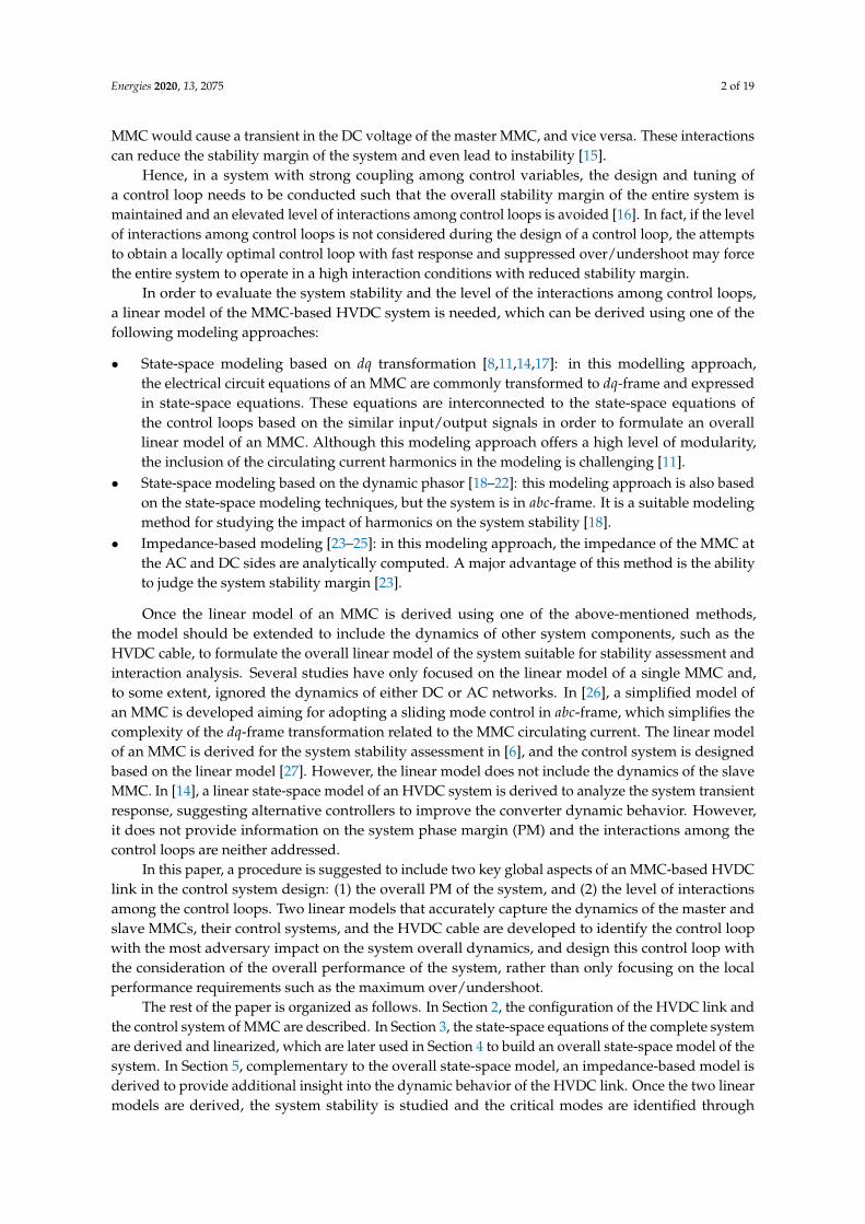
While the eigenvalue analysis and nPF are helpful for detecting not only the critical modes but alsothe main system components contributing to these critical modes, a Nyquist analysis can reveal howfar the system is from instability. In fact, the Nyquist analysis and the associated phase/gain marginsprovide a single index that evaluates the system minimum stability margin. Referring to the impedancemodel of the HVDC link, the Nyquist plot of
(Zs(s)Yl(s)
)is shown in Figure 12, which shows that
the interconnection of the source and the load would be stable (for the cable length of 100 km) and
Energies 2020, 13, 2075 11 of 19
the system stability would have the minimum margins of PM = −22.6 (at frequency 395 rad/s) andGM = −16.1 dB.
0.38 0.42 0.46 0.5 0.54
500
520
540
P1 [
MW
]
Time [s]0.38 0.42 0.46 0.5 0.54
640
650
660
V
t [k
V]
dc
Time [s]
0.38 0.42 0.46 0.5 0.54
1250
1300
1350
Time [s]
i q [
A]
0.38 0.42 0.46 0.5 0.54
24.57
24.58
24.59
24.60
W
t [M
J]
nonlinear model linear model
-400 -350 -300 -250 -200 -150 -100 -50 0
-5
0
5 104
50
100
150
200
250
-70 -60 -50 -40 -30 -20 -10 0
-20
-10
0
10
20
50
100
150
200
250
5
5
Imag
inar
y P
art
Real Part
Imag
inar
y P
art
104 C
able
Len
gth
[km
]C
able
Len
gth
[km
]
0.4 0.45 0.50 0.55 0.60 0.65 0.70 0.75
550
600
650
700
0.40 0.45 0.50 0.55 0.60 0.65 0.70 0.75
24.4
24.6
24.8
Wt1
[M
J]V
t [k
V]
dc
Time [s]
Time [s](b)
(a)
25 km100 km
200 km
25 km100 km
200 km
-100 -80 -60 -40 -20 0 20
-400
-200
0
200
400
0.4
0.6
0.8
1
Imag
inar
y P
art
Real Part
dc v
oltage
contr
oller gain
0.4 0.45 0.50 0.55 0.60 0.65 0.70 0.75 0.80
600
650
700
G=1.0
G=0.8
G=0.6
Vt
[kV
]d
c
Time [s](a)
0.40 0.45 0.50 0.55 0.60 0.65 0.70 0.75 0.8024.4
24.5
24.6
24.7
24.8
Time [s](b)
G=1.0
G=0.8
G=0.6
Wt1
[M
J]
0 0.01 0.02 0.03 0.04 0.05
-1
-0.5
0
0.5
1
1.5
2
Time [s]
Wt1*
Wt2*
vg1q
vg2q
0 0.02 0.04 0.06 0.08 0.1 0.12
-4
-2
0
2(a)
Time [s](b)
Wt2*
vg1q
vg2q
Vt [V
]d
c
Wt1
[J]
vs+-
Zs Zl
+-
vl
-
+v
MMC 1 MMC 2
DC
AC
AC
DC
Zs Zl
5 10 15 20 25 30 35 40
Eigenvalue Index
0
20
40
60
80
100
Dam
pin
g R
atio
[%]
1 43
A
B
C D
Cable parametersA DC voltage PI controller of MMC 1
PLL of MMC 1
B
C PLL of MMC 2D
-10 -8 -6 -4 -2 0 2-1
-0.5
0
0.5
1
Imag
inar
y P
art
Real Part
PM= -22.6°
GM= -16.1 [dB]
-80 -60 -40 -20 0 20 40 60 80Real Part
-1000
0
1000
Im
ag
ina
ry P
art
50
100
150
200
250
15 Cab
le L
eng
th [
km
]
10 25 40 55 70 85 100 115 130 145 160 175 190 200
Cable Length [Km]
-30
-20
-10
0
10
Phase
Marg
in [
deg
ree]
25
0
5
10
15
(b)
(a)
ΔVtdc* ΔP2
* ΔWt1* ΔWt2
*
Trga (s)inputs
outputs
1
ΔVtdc
ΔP2 ΔWt1 ΔWt2
2 3 4
1 2 3 4
100
101
102 10 3-200
-100
0
-40
-20
0
-200
-100
0
-200
-100
0
Frequency [rad/s]
[dB
]
(a)
RG
A V
t dc
[dB
]R
GA
P2
100
101
102 10 3
Frequency [rad/s](b)
[dB
]R
GA
Wt1
100
101
102 10 3
Frequency [rad/s](c)
[dB
]R
GA
Wt2
100
101
102 10 3
Frequency [rad/s](d)
Vt dc P2
*
* * * *
Wc=395 rad/s
Figure 12. The Nyquist plot of(Zs(s)Yl(s)
)of the HVDC link with a cable length of 100 km.
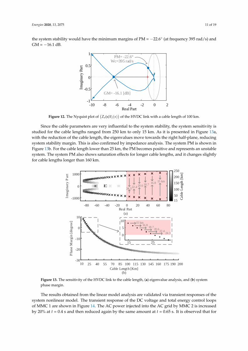
Since the cable parameters are very influential to the system stability, the system sensitivity isstudied for the cable lengths ranged from 250 km to only 15 km. As it is presented in Figure 13a,with the reduction of the cable length, the eigenvalues move towards the right half-plane, reducingsystem stability margin. This is also confirmed by impedance analysis. The system PM is shown inFigure 13b. For the cable length lower than 25 km, the PM becomes positive and represents an unstablesystem. The system PM also shows saturation effects for longer cable lengths, and it changes slightlyfor cable lengths longer than 160 km.0.38 0.42 0.46 0.5 0.54
500
520
540
P1 [
MW
]
Time [s]0.38 0.42 0.46 0.5 0.54
640
650
660
V
t [k
V]
dc
Time [s]
0.38 0.42 0.46 0.5 0.54
1250
1300
1350
Time [s]
i q [
A]
0.38 0.42 0.46 0.5 0.54
24.57
24.58
24.59
24.60
W
t [M
J]
nonlinear model linear model
-400 -350 -300 -250 -200 -150 -100 -50 0
-5
0
5 104
50
100
150
200
250
-70 -60 -50 -40 -30 -20 -10 0
-20
-10
0
10
20
50
100
150
200
250
5
5
Imag
inar
y P
art
Real Part
Imag
inar
y P
art
104 C
ab
le L
eng
th [
km
]C
ab
le L
eng
th [
km
]
0.4 0.45 0.50 0.55 0.60 0.65 0.70 0.75
550
600
650
700
0.40 0.45 0.50 0.55 0.60 0.65 0.70 0.75
24.4
24.6
24.8
Wt1
[M
J]V
t [k
V]
dc
Time [s]
Time [s](b)
(a)
25 km100 km
200 km
25 km100 km
200 km
-100 -80 -60 -40 -20 0 20
-400
-200
0
200
400
0.4
0.6
0.8
1
Imag
inar
y P
art
Real Part
dc v
olt
ag
e co
ntr
oll
er
gain
0.4 0.45 0.50 0.55 0.60 0.65 0.70 0.75 0.80
600
650
700
G=1.0
G=0.8
G=0.6
Vt
[kV
]d
c
Time [s](a)
0.40 0.45 0.50 0.55 0.60 0.65 0.70 0.75 0.8024.4
24.5
24.6
24.7
24.8
Time [s](b)
G=1.0
G=0.8
G=0.6
Wt1
[M
J]
0 0.01 0.02 0.03 0.04 0.05
-1
-0.5
0
0.5
1
1.5
2
Time [s]
Wt1*
Wt2*
vg1q
vg2q
0 0.02 0.04 0.06 0.08 0.1 0.12
-4
-2
0
2(a)
Time [s](b)
Wt2*
vg1q
vg2q
Vt
[V]
dc
Wt1
[J]
vs+-
Zs Zl
+-
vl
-
+v
MMC 1 MMC 2
DC
AC
AC
DC
Zs Zl
5 10 15 20 25 30 35 40
Eigenvalue Index
0
20
40
60
80
100
Dam
pin
g R
atio
[%]
1 43
A
B
C D
Cable parametersA DC voltage PI controller of MMC 1
PLL of MMC 1
B
C PLL of MMC 2D
-10 -8 -6 -4 -2 0 2-1
-0.5
0
0.5
1
Imag
inar
y Pa
rt
Real Part
PM= -22.6°
GM= -16.1 [dB]
-80 -60 -40 -20 0 20 40 60 80Real Part
-1000
0
1000
Im
ag
ina
ry P
art
50
100
150
200
250
15 Cab
le L
eng
th [
km
]
10 25 40 55 70 85 100 115 130 145 160 175 190 200
Cable Length [Km]
-30
-20
-10
0
10
Phase
Marg
in [
deg
ree]
25
0
5
10
15
(b)
(a)
ΔVtdc* ΔP2
* ΔWt1* ΔWt2
*
Trga (s)inputs
outputs
1
ΔVtdc
ΔP2 ΔWt1 ΔWt2
2 3 4
1 2 3 4 100
101
102 10 3-200
-100
0
-40
-20
0
-200
-100
0
-200
-100
0
Frequency [rad/s]
[dB
]
(a)
RG
A V
t dc
[dB
]R
GA
P2
100
101
102 10 3
Frequency [rad/s](b)
[dB
]R
GA
Wt1
100
101
102 10 3
Frequency [rad/s](c)
[dB
]R
GA
Wt2
100
101
102 10 3
Frequency [rad/s](d)
Vt dc P2 * * *
Wc=395 rad/s
0.5
1
1.5
5
10
0.1
DC
Vo
ltag
e P
I G
ain
(k
g)
0.5 1 1.5-25
-22
-19
Largest PM
Largest PM
(a)
(b)
High interactions among
control loops
0
1
2
100
101
102 10 3
[ab
s]R
GA
Vt d
c
Frequency [rad/s](a)
0
0.5
1
1.5
100
101
102 10 3
Frequency [rad/s](b)
[ab
s]R
GA
P2
0
1
2
100
101
102 10 3
[ab
s]R
GA
Wt1
Frequency [rad/s](c)
0
1
2
[ab
s]R
GA
Wt2
100
101
102 10 3
Frequency [rad/s](d)
Vt dc P2 * * * *
[abs]
RG
A V
t dc
*
Vt dc*
P2 *
*
Frequency [rad/s]
[abs]
RG
A V
t dc
Vt dc*
Vt dc*
Vt dc*
(Stable system)
(Unstable system)
(Largest PM)
(a)
Frequency [rad/s](b)
G=0.55 (ic=12) optimum performance
DC Voltage PI Gain (kg)
Color of unstable poles
15 km
16.818.720.622.4
24.3
15 km16.818.720.622.424.315 km
16.818.7
20.622.4
24.3
Vt dc P2 * * * *
kg=0.2
[ab
s]R
GA
Vt d
c
Frequency [rad/s](a)
[ab
s]R
GA
Vt d
c
Frequency [rad/s](b)
kg=0.55
Frequency [rad/s](c)
[ab
s]R
GA
Vt d
c
kg=2.5
103
Frequency [rad/s](d)
101
kg=5
[ab
s]R
GA
Vt d
c
Vt
[kV
]d
c
Time [s]
kg = 0.55kg = 2.5kg = 5kg = 0.2
Figure 13. The sensitivity of the HVDC link to the cable length, (a) eigenvalue analysis, and (b) systemphase margin.
The results obtained from the linear model analysis are validated via transient responses of thesystem nonlinear model. The transient response of the DC voltage and total energy control loopsof MMC 1 are shown in Figure 14. The AC power injected into the AC grid by MMC 2 is increasedby 20% at t = 0.4 s and then reduced again by the same amount at t = 0.65 s. It is observed that for

Energies 2020, 13, 2075 12 of 19
the shorter cable length, the system exhibits higher oscillations (lower damping and smaller PM),which is consistent with the linear analysis.
-400 -350 -300 -250 -200 -150 -100 -50 0
-5
0
5 104
50
100
150
200
250
-70 -60 -50 -40 -30 -20 -10 0
-20
-10
0
10
20
50
100
150
200
250
5
5
Imag
inar
y P
art
Real Part
Imag
inar
y P
art
104 C
able
Len
gth
[km
]C
able
Len
gth
[km
]
0.4 0.45 0.50 0.55 0.60 0.65 0.70 0.75550
600
650
700
0.40 0.45 0.50 0.55 0.60 0.65 0.70 0.75
24.4
24.6
24.8
Wt1
[M
J]V
t [kV
]dc
Time [s]
Time [s](b)
(a)
25 km100 km200 km
25 km100 km200 km
Figure 14. The transient response of (a) DC voltage and (b) the total energy control loops of MMC 1 forthree different cable lengths.
6.2. System Interactions
Referring to Figure 4, there are four major cascaded control loops (two control loops per MMC)in the HVDC link: Vdc
t , P2, Wt1, and Wt2. The control loops of MMC 1 interact with those of MMC 2through the HVDC cable. For instance, a step change in the total energy of MMC 2 (step changein the reference W∗t2) would have impact on the DC voltage Vdc
t of MMC 1. In order to quantifythese interactions, a frequency-dependant RGA analysis is conducted on the MIMO model shown inFigure 15, which includes the control loop references as the inputs, and the controlled variables asthe outputs.
0.38 0.42 0.46 0.5 0.54
500
520
540
P1 [
MW
]
Time [s]0.38 0.42 0.46 0.5 0.54
640
650
660
V
t [k
V]
dc
Time [s]
0.38 0.42 0.46 0.5 0.54
1250
1300
1350
Time [s]
i q [
A]
0.38 0.42 0.46 0.5 0.54
24.57
24.58
24.59
24.60
W
t [M
J]
nonlinear model linear model
-400 -350 -300 -250 -200 -150 -100 -50 0
-5
0
5 104
50
100
150
200
250
-70 -60 -50 -40 -30 -20 -10 0
-20
-10
0
10
20
50
100
150
200
250
5
5
Imag
inar
y P
art
Real Part
Imag
inar
y P
art
104 C
able
Len
gth
[km
]C
able
Len
gth
[km
]
0.4 0.45 0.50 0.55 0.60 0.65 0.70 0.75
550
600
650
700
0.40 0.45 0.50 0.55 0.60 0.65 0.70 0.75
24.4
24.6
24.8
Wt1
[M
J]V
t [k
V]
dc
Time [s]
Time [s](b)
(a)
25 km100 km
200 km
25 km100 km
200 km
-100 -80 -60 -40 -20 0 20
-400
-200
0
200
400
0.4
0.6
0.8
1
Imag
inar
y P
art
Real Part
dc v
oltage
contr
oller gain
0.4 0.45 0.50 0.55 0.60 0.65 0.70 0.75 0.80
600
650
700
G=1.0
G=0.8
G=0.6
Vt
[kV
]d
c
Time [s](a)
0.40 0.45 0.50 0.55 0.60 0.65 0.70 0.75 0.8024.4
24.5
24.6
24.7
24.8
Time [s](b)
G=1.0
G=0.8
G=0.6
Wt1
[M
J]
0 0.01 0.02 0.03 0.04 0.05
-1
-0.5
0
0.5
1
1.5
2
Time [s]
Wt1*
Wt2*
vg1q
vg2q
0 0.02 0.04 0.06 0.08 0.1 0.12
-4
-2
0
2(a)
Time [s](b)
Wt2*
vg1q
vg2q
Vt [V
]d
c
Wt1
[J]
vs+-
Zs Zl
+-
vl
-
+v
MMC 1 MMC 2
DC
AC
AC
DC
Zs Zl
5 10 15 20 25 30 35 40
Eigenvalue Index
0
20
40
60
80
100
Dam
pin
g R
atio
[%]
1 43
A
B
C D
Cable parametersA DC voltage PI controller of MMC 1
PLL of MMC 1
B
C PLL of MMC 2D
-10 -8 -6 -4 -2 0 2-1
-0.5
0
0.5
1
Imag
inar
y P
art
Real Part
PM= -22.6°
GM= -16.1 [dB]
-80 -60 -40 -20 0 20 40 60 80Real Part
-1000
0
1000
Im
ag
ina
ry P
art
50
100
150
200
250
15 Cable
Len
gth
[km
]
10 25 40 55 70 85 100 115 130 145 160 175 190 200
Cable Length [Km]
-30
-20
-10
0
10
Phase
Marg
in [
deg
ree]
25
0
5
10
15
(b)
(a)
ΔVtdc* ΔP2
* ΔWt1* ΔWt2
*
Trga (s)
inputs
outputs
1
ΔVtdc
ΔP2 ΔWt1 ΔWt2
2 3 4
1 2 3 4
Figure 15. The MIMO model of the system used for relative gain array (RGA) analysis.
The results of the RGA analysis are presented in Figure 16. It can be observed that
• At low frequencies, all four control loops are strongly coupled with their own references,i.e., the RGA values between the controlled variables (such as Vdc
t ) and the loop references(such as Vdc∗
t ) are the largest as compared with the RGA values related to other control loopreferences. Hence, the four control loops are well-designed for DC or low frequencies.
• The active power control loop P2 does not interact with other three control loops (Vdct , Wt1,
and Wt2), and it is only coupled with its own reference.

Energies 2020, 13, 2075 13 of 19
• At higher frequencies, the control loops begin to interact. As it can be seen from Figure 16,at the frequencies near 400 rad/s, the RGA values increase, meaning that a controlled variable isimportantly affected by the references of other control loops.
• Reference values should be changed with a limited bandwidth lower than 400 rad/s to avoidinteractions between loops.
The RGA analysis identifies the frequency range in which the control loop interactions becomesignificant. The control loops in the HVDC link highly interact with each other near frequency400 rad/s (for the cable length of 100 km). Interestingly, the system minimum PM (see Figure 12)happens near this frequency as well. It can be concluded that the interactions among control loopsmay have an influence on the system minimum PM.
0.38 0.42 0.46 0.5 0.54
500
520
540
P1 [
MW
]
Time [s]0.38 0.42 0.46 0.5 0.54
640
650
660
V
t [k
V]
dc
Time [s]
0.38 0.42 0.46 0.5 0.54
1250
1300
1350
Time [s]
i q [
A]
0.38 0.42 0.46 0.5 0.54
24.57
24.58
24.59
24.60
W
t [M
J]
nonlinear model linear model
-400 -350 -300 -250 -200 -150 -100 -50 0
-5
0
5 104
50
100
150
200
250
-70 -60 -50 -40 -30 -20 -10 0
-20
-10
0
10
20
50
100
150
200
250
5
5
Imag
inar
y P
art
Real Part
Imag
inar
y P
art
104 C
ab
le L
eng
th [
km
]C
ab
le L
eng
th [
km
]
0.4 0.45 0.50 0.55 0.60 0.65 0.70 0.75
550
600
650
700
0.40 0.45 0.50 0.55 0.60 0.65 0.70 0.75
24.4
24.6
24.8
Wt1
[M
J]V
t [k
V]
dc
Time [s]
Time [s](b)
(a)
25 km100 km
200 km
25 km100 km
200 km
-100 -80 -60 -40 -20 0 20
-400
-200
0
200
400
0.4
0.6
0.8
1
Imag
inar
y P
art
Real Part
dc v
olt
ag
e co
ntr
oll
er
gain
0.4 0.45 0.50 0.55 0.60 0.65 0.70 0.75 0.80
600
650
700
G=1.0
G=0.8
G=0.6
Vt
[kV
]d
c
Time [s](a)
0.40 0.45 0.50 0.55 0.60 0.65 0.70 0.75 0.8024.4
24.5
24.6
24.7
24.8
Time [s](b)
G=1.0
G=0.8
G=0.6
Wt1
[M
J]
0 0.01 0.02 0.03 0.04 0.05
-1
-0.5
0
0.5
1
1.5
2
Time [s]
Wt1*
Wt2*
vg1q
vg2q
0 0.02 0.04 0.06 0.08 0.1 0.12
-4
-2
0
2(a)
Time [s](b)
Wt2*
vg1q
vg2q
Vt
[V]
dc
Wt1
[J]
vs+-
Zs Zl
+-
vl
-
+v
MMC 1 MMC 2
DC
AC
AC
DC
Zs Zl
5 10 15 20 25 30 35 40
Eigenvalue Index
0
20
40
60
80
100
Dam
pin
g R
atio
[%]
1 43
A
B
C D
Cable parametersA DC voltage PI controller of MMC 1
PLL of MMC 1
B
C PLL of MMC 2D
-10 -8 -6 -4 -2 0 2-1
-0.5
0
0.5
1
Imag
inar
y Pa
rt
Real Part
PM= -22.6°
GM= -16.1 [dB]
-80 -60 -40 -20 0 20 40 60 80Real Part
-1000
0
1000
Im
ag
ina
ry P
art
50
100
150
200
250
15 Cab
le L
eng
th [
km
]
10 25 40 55 70 85 100 115 130 145 160 175 190 200
Cable Length [Km]
-30
-20
-10
0
10
Phase
Marg
in [
deg
ree]
25
0
5
10
15
(b)
(a)
ΔVtdc* ΔP2
* ΔWt1* ΔWt2
*
Trga (s)inputs
outputs
1
ΔVtdc
ΔP2 ΔWt1 ΔWt2
2 3 4
1 2 3 4 100
101
102 10 3-200
-100
0
-40
-20
0
-200
-100
0
-200
-100
0
Frequency [rad/s]
[dB
]
(a)
RG
A V
t dc
[dB
]R
GA
P2
100
101
102 10 3
Frequency [rad/s](b)
[dB
]R
GA
Wt1
100
101
102 10 3
Frequency [rad/s](c)
[dB
]R
GA
Wt2
100
101
102 10 3
Frequency [rad/s](d)
Vt dc P2 * * *
Wc=395 rad/s
0.5
1
1.5
5
10
0.1 DC
Vo
ltag
e P
I G
ain
(G
)
0.5 1 1.5-25
-22
-19
Largest PM
Largest PM
(a)
(b)
High interactions among
control loops
0
1
2
100
101
102 10 3
[ab
s]R
GA
Vt d
c
Frequency [rad/s](a)
0
0.5
1
1.5
100
101
102 10 3
Frequency [rad/s](b)
[ab
s]R
GA
P2
0
1
2
100
101
102 10 3
[ab
s]R
GA
Wt1
Frequency [rad/s](c)
0
1
2
[ab
s]R
GA
Wt2
100
101
102 10 3
Frequency [rad/s](d)
Vt dc P2 * * * *
[abs]
RG
A V
t dc
*
Vt dc*
P2 *
*
Frequency [rad/s]
[abs]
RG
A V
t dc
Vt dc*
Vt dc*
Vt dc*
(Stable system)
(Unstable system)
(Largest PM)
(a)
Frequency [rad/s](b)
G=0.55 (ic=12) optimum performance
DC Voltage PI Gain (G)
Figure 16. The RGA of four main control loops.
7. DC Voltage Control Loop Design
The results obtained in the previous section can be used to improve the system performance.The following conclusions have been extracted from the HVDC 100 km link case study:

Energies 2020, 13, 2075 14 of 19
• The HVDC link has 10 eigenvalues (critical modes) with a damping ratio lower than 5%,which are related to the cable parameters. The frequency of these modes are in order of104 rad/s (see Figure 11).
• There are two (conjugate) eigenvalues with a low damping ratio (about 22%) that belong to the PIcontroller of the DC voltage control loop. Their frequency is near 400 rad/s (see Figure 11).
• The minimum PM of the HVDC link is −22.6 and occurs at the frequency near 400 rad/s(see Figure 12).
• The interactions among the control loops of the HVDC link begin to intensify at the frequenciesnear 400 rad/s (see Figure 16).
• The PI controller of the DC voltage controller should be adequately designed to improve thesystem dynamics since it is the loop that is mainly contributing to the system modes allocatedclose to the problematic frequency 400 rad/s.
Then, assuming the cable length is already fixed at 100 km, the dynamics of Vdct control loop
can be simply improved by finding the right gains that improve the control loop performance.Initially, the proportional and integral gains of the PI controller are set to 0.002 and 0.708, respectively.These values are determined to make the outer control loop (Vdc
t ) 15 times slower than the inner controlloop. Then, both the proportional and integral gains of the PI controller are multiplied by a constant kg
to find the case which is stable and has the largest PM. To do this, kg is varied from 0.1 to 10.The system dominant eigenvalues for the range of kg are shown in Figure 17a. The system is
unstable for kg smaller than 0.2 and bigger than 5. For all other values of kg between 0.2 to 5 thesystem is stable. The largest system PM occurs at kg equal to 0.55 as it is presented in Figure 17b.Thus, kg equal to 0.55 can be selected as an adequate design candidate.
0.38 0.42 0.46 0.5 0.54
500
520
540
P1 [
MW
]
Time [s]0.38 0.42 0.46 0.5 0.54
640
650
660
V
t [k
V]
dc
Time [s]
0.38 0.42 0.46 0.5 0.54
1250
1300
1350
Time [s]
i q [
A]
0.38 0.42 0.46 0.5 0.54
24.57
24.58
24.59
24.60
W
t [M
J]
nonlinear model linear model
-400 -350 -300 -250 -200 -150 -100 -50 0
-5
0
5 104
50
100
150
200
250
-70 -60 -50 -40 -30 -20 -10 0
-20
-10
0
10
20
50
100
150
200
250
5
5
Imag
inar
y P
art
Real Part
Imag
inar
y P
art
104 C
able
Len
gth
[km
]C
able
Len
gth
[km
]
0.4 0.45 0.50 0.55 0.60 0.65 0.70 0.75
550
600
650
700
0.40 0.45 0.50 0.55 0.60 0.65 0.70 0.75
24.4
24.6
24.8
Wt1
[M
J]V
t [k
V]
dc
Time [s]
Time [s](b)
(a)
25 km100 km
200 km
25 km100 km
200 km
-100 -80 -60 -40 -20 0 20
-400
-200
0
200
400
0.4
0.6
0.8
1
Imag
inar
y P
art
Real Part
dc v
oltage
contr
oller gain
0.4 0.45 0.50 0.55 0.60 0.65 0.70 0.75 0.80
600
650
700
G=1.0
G=0.8
G=0.6
Vt
[kV
]d
c
Time [s](a)
0.40 0.45 0.50 0.55 0.60 0.65 0.70 0.75 0.8024.4
24.5
24.6
24.7
24.8
Time [s](b)
G=1.0
G=0.8
G=0.6
Wt1
[M
J]
0 0.01 0.02 0.03 0.04 0.05
-1
-0.5
0
0.5
1
1.5
2
Time [s]
Wt1*
Wt2*
vg1q
vg2q
0 0.02 0.04 0.06 0.08 0.1 0.12
-4
-2
0
2(a)
Time [s](b)
Wt2*
vg1q
vg2q
Vt
[V]
dc
Wt1
[J]
vs+-
Zs Zl
+-
vl
-
+v
MMC 1 MMC 2
DC
AC
AC
DC
Zs Zl
5 10 15 20 25 30 35 40
Eigenvalue Index
0
20
40
60
80
100
Dam
pin
g R
atio
[%]
1 43
A
B
C D
Cable parametersA DC voltage PI controller of MMC 1
PLL of MMC 1
B
C PLL of MMC 2D
-10 -8 -6 -4 -2 0 2-1
-0.5
0
0.5
1
Imag
inar
y Pa
rt
Real Part
PM= -22.6°
GM= -16.1 [dB]
-80 -60 -40 -20 0 20 40 60 80Real Part
-1000
0
1000
Im
ag
ina
ry P
art
50
100
150
200
250
15 Cable
Len
gth
[km
]
10 25 40 55 70 85 100 115 130 145 160 175 190 200
Cable Length [Km]
-30
-20
-10
0
10
Phase
Marg
in [
deg
ree]
25
0
5
10
15
(b)
(a)
ΔVtdc* ΔP2
* ΔWt1* ΔWt2
*
Trga (s)inputs
outputs
1
ΔVtdc
ΔP2 ΔWt1 ΔWt2
2 3 4
1 2 3 4 100
101
102 10 3-200
-100
0
-40
-20
0
-200
-100
0
-200
-100
0
Frequency [rad/s]
[dB
]
(a)
RG
A V
t dc
[dB
]R
GA
P2
100
101
102 10 3
Frequency [rad/s](b)
[dB
]R
GA
Wt1
100
101
102 10 3
Frequency [rad/s](c)
[dB
]R
GA
Wt2
100
101
102 10 3
Frequency [rad/s](d)
Vt dc P2 * * *
Wc=395 rad/s
0.5
1
1.5
5
10
0.1
DC
Voltage
PI
Gain
(k
g)
0.5 1 1.5-25
-22
-19
Largest PM
Largest PM
(a)
(b)
High interactions among
control loops
0
1
2
100
101
102 10 3
[ab
s]R
GA
Vt d
c
Frequency [rad/s](a)
0
0.5
1
1.5
100
101
102 10 3
Frequency [rad/s](b)
[abs]
RG
A P
2
0
1
2
100
101
102 10 3
[abs]
RG
A W
t1
Frequency [rad/s](c)
0
1
2
[abs]
RG
A W
t2
100
101
102 10 3
Frequency [rad/s](d)
Vt dc P2 * * * *
[abs]
RG
A V
t dc
*
Vt dc*
P2 *
*
Frequency [rad/s]
[abs]
RG
A V
t dc
Vt dc*
Vt dc*
Vt dc*
(Stable system)
(Unstable system)
(Largest PM)
(a)
Frequency [rad/s](b)
G=0.55 (ic=12) optimum performance
DC Voltage PI Gain (kg)
Color of unstable polesFigure 17. The impact of DC voltage PI gain (kg) on the system dynamics, (a) the system dominanteigenvalues, (b) the system phase margin.
The next step is to carry out RGA analysis in order to observe the level of control loop interactionsfor various values of kg. The RGA values of Vdc
t for the entire range of kg (from 0.1 to 10) are presentedin Figure 18. Within two frequency bands, the RGA values exhibit large peaks, which indicate highlevel of interactions among control loops. The RGA values related to the design candidate (kg = 0.55)

Energies 2020, 13, 2075 15 of 19
should not have large peaks within the system frequency range which is confirmed from Figure 19.For the sake of clarity, the RGA analysis is conducted for fewer kg values (0.2, 0.55, 2.5, 5) within thedefined stable range. Clearly, the RGA values for kg = 0.55 does not present large peaks, confirmingthe adequacy of the design candidate.
0.38 0.42 0.46 0.5 0.54
500
520
540
P1 [
MW
]
Time [s]0.38 0.42 0.46 0.5 0.54
640
650
660
V
t [k
V]
dc
Time [s]
0.38 0.42 0.46 0.5 0.54
1250
1300
1350
Time [s]
i q [
A]
0.38 0.42 0.46 0.5 0.54
24.57
24.58
24.59
24.60
W
t [M
J]
nonlinear model linear model
-400 -350 -300 -250 -200 -150 -100 -50 0
-5
0
5 104
50
100
150
200
250
-70 -60 -50 -40 -30 -20 -10 0
-20
-10
0
10
20
50
100
150
200
250
5
5
Imag
inar
y P
art
Real Part
Imag
inar
y P
art
104 C
able
Len
gth
[km
]C
able
Len
gth
[km
]
0.4 0.45 0.50 0.55 0.60 0.65 0.70 0.75
550
600
650
700
0.40 0.45 0.50 0.55 0.60 0.65 0.70 0.75
24.4
24.6
24.8
Wt1
[M
J]V
t [k
V]
dc
Time [s]
Time [s](b)
(a)
25 km100 km
200 km
25 km100 km
200 km
-100 -80 -60 -40 -20 0 20
-400
-200
0
200
400
0.4
0.6
0.8
1
Imag
inar
y P
art
Real Part
dc v
oltage
contr
oller gain
0.4 0.45 0.50 0.55 0.60 0.65 0.70 0.75 0.80
600
650
700
G=1.0
G=0.8
G=0.6
Vt
[kV
]d
c
Time [s](a)
0.40 0.45 0.50 0.55 0.60 0.65 0.70 0.75 0.8024.4
24.5
24.6
24.7
24.8
Time [s](b)
G=1.0
G=0.8
G=0.6
Wt1
[M
J]
0 0.01 0.02 0.03 0.04 0.05
-1
-0.5
0
0.5
1
1.5
2
Time [s]
Wt1*
Wt2*
vg1q
vg2q
0 0.02 0.04 0.06 0.08 0.1 0.12
-4
-2
0
2(a)
Time [s](b)
Wt2*
vg1q
vg2q
Vt
[V]
dc
Wt1
[J]
vs+-
Zs Zl
+-
vl
-
+v
MMC 1 MMC 2
DC
AC
AC
DC
Zs Zl
5 10 15 20 25 30 35 40
Eigenvalue Index
0
20
40
60
80
100
Dam
pin
g R
atio
[%]
1 43
A
B
C D
Cable parametersA DC voltage PI controller of MMC 1
PLL of MMC 1
B
C PLL of MMC 2D
-10 -8 -6 -4 -2 0 2-1
-0.5
0
0.5
1
Imag
inar
y Pa
rt
Real Part
PM= -22.6°
GM= -16.1 [dB]
-80 -60 -40 -20 0 20 40 60 80Real Part
-1000
0
1000
Im
ag
ina
ry P
art
50
100
150
200
250
15 Cable
Len
gth
[km
]
10 25 40 55 70 85 100 115 130 145 160 175 190 200
Cable Length [Km]
-30
-20
-10
0
10
Phase
Marg
in [
deg
ree]
25
0
5
10
15
(b)
(a)
ΔVtdc* ΔP2
* ΔWt1* ΔWt2
*
Trga (s)inputs
outputs
1
ΔVtdc
ΔP2 ΔWt1 ΔWt2
2 3 4
1 2 3 4 100
101
102 10 3-200
-100
0
-40
-20
0
-200
-100
0
-200
-100
0
Frequency [rad/s]
[dB
]
(a)
RG
A V
t dc
[dB
]R
GA
P2
100
101
102 10 3
Frequency [rad/s](b)
[dB
]R
GA
Wt1
100
101
102 10 3
Frequency [rad/s](c)
[dB
]R
GA
Wt2
100
101
102 10 3
Frequency [rad/s](d)
Vt dc P2 * * *
Wc=395 rad/s
0.5
1
1.5
5
10
0.1
DC
Voltage
PI
Gain
(k
g)
0.5 1 1.5-25
-22
-19
Largest PM
Largest PM
(a)
(b)
High interactions among
control loops
0
1
2
100
101
102 10 3
[ab
s]R
GA
Vt d
c
Frequency [rad/s](a)
0
0.5
1
1.5
100
101
102 10 3
Frequency [rad/s](b)
[abs]
RG
A P
2
0
1
2
100
101
102 10 3
[abs]
RG
A W
t1
Frequency [rad/s](c)
0
1
2
[abs]
RG
A W
t2
100
101
102 10 3
Frequency [rad/s](d)
Vt dc P2 * * * *
[abs]
RG
A V
t dc
*
Vt dc*
P2 *
*
Frequency [rad/s]
[abs]
RG
A V
t dc
Vt dc*
Vt dc*
Vt dc*
(Stable system)
(Unstable system)
(Largest PM)
(a)
Frequency [rad/s](b)
G=0.55 (ic=12) optimum performance
DC Voltage PI Gain (kg)
Color of unstable poles
15 km
16.818.720.622.4
24.3
15 km16.818.720.622.424.315 km
16.818.7
20.622.4
24.3
Vt dc P2 * * * *
kg=0.2
[abs]
RG
A V
t dc
Frequency [rad/s](a)
[abs]
RG
A V
t dc
Frequency [rad/s](b)
kg=0.55
Frequency [rad/s](c)
[ab
s]R
GA
Vt d
c
kg=2.5
103
Frequency [rad/s](d)
101
kg=5
[abs]
RG
A V
t dc
Figure 18. The RGA values of the DC voltage control loop for various PI controller gains (kg).
0.38 0.42 0.46 0.5 0.54
500
520
540
P1 [
MW
]
Time [s]0.38 0.42 0.46 0.5 0.54
640
650
660
V
t [k
V]
dc
Time [s]
0.38 0.42 0.46 0.5 0.54
1250
1300
1350
Time [s]
i q [
A]
0.38 0.42 0.46 0.5 0.54
24.57
24.58
24.59
24.60
W
t [M
J]
nonlinear model linear model
-400 -350 -300 -250 -200 -150 -100 -50 0
-5
0
5 104
50
100
150
200
250
-70 -60 -50 -40 -30 -20 -10 0
-20
-10
0
10
20
50
100
150
200
250
5
5
Imag
inar
y P
art
Real Part
Imag
inar
y P
art
104 C
able
Len
gth
[km
]C
able
Len
gth
[km
]
0.4 0.45 0.50 0.55 0.60 0.65 0.70 0.75
550
600
650
700
0.40 0.45 0.50 0.55 0.60 0.65 0.70 0.75
24.4
24.6
24.8
Wt1
[M
J]V
t [k
V]
dc
Time [s]
Time [s](b)
(a)
25 km100 km
200 km
25 km100 km
200 km
-100 -80 -60 -40 -20 0 20
-400
-200
0
200
400
0.4
0.6
0.8
1
Imag
inar
y P
art
Real Part
dc v
oltage
contr
oller gain
0.4 0.45 0.50 0.55 0.60 0.65 0.70 0.75 0.80
600
650
700
G=1.0
G=0.8
G=0.6
Vt
[kV
]d
c
Time [s](a)
0.40 0.45 0.50 0.55 0.60 0.65 0.70 0.75 0.8024.4
24.5
24.6
24.7
24.8
Time [s](b)
G=1.0
G=0.8
G=0.6
Wt1
[M
J]
0 0.01 0.02 0.03 0.04 0.05
-1
-0.5
0
0.5
1
1.5
2
Time [s]
Wt1*
Wt2*
vg1q
vg2q
0 0.02 0.04 0.06 0.08 0.1 0.12
-4
-2
0
2(a)
Time [s](b)
Wt2*
vg1q
vg2q
Vt
[V]
dc
Wt1
[J]
vs+-
Zs Zl
+-
vl
-
+v
MMC 1 MMC 2
DC
AC
AC
DC
Zs Zl
5 10 15 20 25 30 35 40
Eigenvalue Index
0
20
40
60
80
100
Dam
pin
g R
atio
[%]
1 43
A
B
C D
Cable parametersA DC voltage PI controller of MMC 1
PLL of MMC 1
B
C PLL of MMC 2D
-10 -8 -6 -4 -2 0 2-1
-0.5
0
0.5
1
Imag
inar
y Pa
rt
Real Part
PM= -22.6°
GM= -16.1 [dB]
-80 -60 -40 -20 0 20 40 60 80Real Part
-1000
0
1000
Im
ag
ina
ry P
art
50
100
150
200
250
15 Cable
Len
gth
[km
]
10 25 40 55 70 85 100 115 130 145 160 175 190 200
Cable Length [Km]
-30
-20
-10
0
10
Phase
Marg
in [
deg
ree]
25
0
5
10
15
(b)
(a)
ΔVtdc* ΔP2
* ΔWt1* ΔWt2
*
Trga (s)inputs
outputs
1
ΔVtdc
ΔP2 ΔWt1 ΔWt2
2 3 4
1 2 3 4 100
101
102 10 3-200
-100
0
-40
-20
0
-200
-100
0
-200
-100
0
Frequency [rad/s]
[dB
]
(a)
RG
A V
t dc
[dB
]R
GA
P2
100
101
102 10 3
Frequency [rad/s](b)
[dB
]R
GA
Wt1
10
010
1102 10 3
Frequency [rad/s](c)
[dB
]R
GA
Wt2
100
101
102 10 3
Frequency [rad/s](d)
Vt dc P2 * * *
Wc=395 rad/s
0.5
1
1.5
5
10
0.1
DC
Voltage
PI
Gain
(k
g)
0.5 1 1.5-25
-22
-19
Largest PM
Largest PM
(a)
(b)
High interactions among
control loops
0
1
2
100
101
102 10 3
[ab
s]R
GA
Vt d
c
Frequency [rad/s](a)
0
0.5
1
1.5
100
101
102 10 3
Frequency [rad/s](b)
[abs]
RG
A P
2
0
1
2
100
101
102 10 3
[abs]
RG
A W
t1
Frequency [rad/s](c)
0
1
2
[abs]
RG
A W
t2
100
101
102 10 3
Frequency [rad/s](d)
Vt dc P2 * * * *
[abs]
RG
A V
t dc
*
Vt dc*
P2 *
*
Frequency [rad/s]
[abs]
RG
A V
t dc
Vt dc*
Vt dc*
Vt dc*
(Stable system)
(Unstable system)
(Largest PM)
(a)
Frequency [rad/s](b)
G=0.55 (ic=12) optimum performance
DC Voltage PI Gain (kg)
Color of unstable poles
15 km
16.818.720.622.4
24.3
15 km16.818.720.622.424.315 km
16.818.7
20.622.4
24.3
Vt dc P2 * * * *
kg=0.2
[abs]
RG
A V
t dc
Frequency [rad/s](a)
[abs]
RG
A V
t dc
Frequency [rad/s](b)
kg=0.55
Frequency [rad/s](c)
[ab
s]R
GA
Vt d
c
kg=2.5
103
Frequency [rad/s](d)
101
kg=5
[ab
s]R
GA
Vt d
c
Figure 19. The RGA values of the DC voltage control loop for four values of kg: (a) kg = 0.2, (b) kg = 0.55,(c) kg = 2.5, and (d) kg = 5.
In order to verify the results obtained from the frequency-based design, a time-domain simulationis conducted on the HVDC link for the four values of kg. The dynamic response of DC voltagefor a 20% increase in the injected power (P2) is shown in Figure 20. The DC voltage is poorlydamped for kg = 0.2, 2.5, 5, confirming that the system has low PM for these values. With regard tokg = 0.55 (design candidate), the DC voltage is less oscillatory, although showing a moderate overshoot.Note that the tuning of the DC voltage control loop is carried out considering the PM of the entiresystem, not only focusing on the DC voltage control loop. Thus, even though the DC voltage overshootfor the design case might be a bit higher compared to other kg values, it is able to maximize PM whilereducing the interactions.

Energies 2020, 13, 2075 16 of 19
0.38 0.42 0.46 0.5 0.54
500
520
540
P1 [
MW
]
Time [s]0.38 0.42 0.46 0.5 0.54
640
650
660
V
t [k
V]
dc
Time [s]
0.38 0.42 0.46 0.5 0.54
1250
1300
1350
Time [s]
i q [
A]
0.38 0.42 0.46 0.5 0.54
24.57
24.58
24.59
24.60
W
t [M
J]
nonlinear model linear model
-400 -350 -300 -250 -200 -150 -100 -50 0
-5
0
5 104
50
100
150
200
250
-70 -60 -50 -40 -30 -20 -10 0
-20
-10
0
10
20
50
100
150
200
250
5
5
Imag
inar
y P
art
Real Part
Imag
inar
y P
art
104 C
ab
le L
eng
th [
km
]C
ab
le L
eng
th [
km
]
0.4 0.45 0.50 0.55 0.60 0.65 0.70 0.75
550
600
650
700
0.40 0.45 0.50 0.55 0.60 0.65 0.70 0.75
24.4
24.6
24.8
Wt1
[M
J]V
t [k
V]
dc
Time [s]
Time [s](b)
(a)
25 km100 km
200 km
25 km100 km
200 km
-100 -80 -60 -40 -20 0 20
-400
-200
0
200
400
0.4
0.6
0.8
1
Imag
inar
y P
art
Real Part
dc v
olt
ag
e co
ntr
oll
er
gain
0.4 0.45 0.50 0.55 0.60 0.65 0.70 0.75 0.80
600
650
700
G=1.0
G=0.8
G=0.6
Vt
[kV
]d
c
Time [s](a)
0.40 0.45 0.50 0.55 0.60 0.65 0.70 0.75 0.8024.4
24.5
24.6
24.7
24.8
Time [s](b)
G=1.0
G=0.8
G=0.6
Wt1
[M
J]
0 0.01 0.02 0.03 0.04 0.05
-1
-0.5
0
0.5
1
1.5
2
Time [s]
Wt1*
Wt2*
vg1q
vg2q
0 0.02 0.04 0.06 0.08 0.1 0.12
-4
-2
0
2(a)
Time [s](b)
Wt2*
vg1q
vg2q
Vt
[V]
dc
Wt1
[J]
vs+-
Zs Zl
+-
vl
-
+v
MMC 1 MMC 2
DC
AC
AC
DC
Zs Zl
5 10 15 20 25 30 35 40
Eigenvalue Index
0
20
40
60
80
100
Dam
pin
g R
atio
[%]
1 43
A
B
C D
Cable parametersA DC voltage PI controller of MMC 1
PLL of MMC 1
B
C PLL of MMC 2D
-10 -8 -6 -4 -2 0 2-1
-0.5
0
0.5
1
Imag
inar
y Pa
rt
Real Part
PM= -22.6°
GM= -16.1 [dB]
-80 -60 -40 -20 0 20 40 60 80Real Part
-1000
0
1000
Im
ag
ina
ry P
art
50
100
150
200
250
15 Cab
le L
eng
th [
km
]
10 25 40 55 70 85 100 115 130 145 160 175 190 200
Cable Length [Km]
-30
-20
-10
0
10
Phase
Marg
in [
deg
ree]
25
0
5
10
15
(b)
(a)
ΔVtdc* ΔP2
* ΔWt1* ΔWt2
*
Trga (s)inputs
outputs
1
ΔVtdc
ΔP2 ΔWt1 ΔWt2
2 3 4
1 2 3 4 100
101
102 10 3-200
-100
0
-40
-20
0
-200
-100
0
-200
-100
0
Frequency [rad/s]
[dB
]
(a)
RG
A V
t dc
[dB
]R
GA
P2
100
101
102 10 3
Frequency [rad/s](b)
[dB
]R
GA
Wt1
100
101
102 10 3
Frequency [rad/s](c)
[dB
]R
GA
Wt2
100
101
102 10 3
Frequency [rad/s](d)
Vt dc P2 * * *
Wc=395 rad/s
0.5
1
1.5
5
10
0.1
DC
Vo
ltag
e P
I G
ain
(k
g)
0.5 1 1.5-25
-22
-19
Largest PM
Largest PM
(a)
(b)
High interactions among
control loops
0
1
2
100
101
102 10 3
[ab
s]R
GA
Vt d
c
Frequency [rad/s](a)
0
0.5
1
1.5
100
101
102 10 3
Frequency [rad/s](b)
[ab
s]R
GA
P2
0
1
2
100
101
102 10 3
[ab
s]R
GA
Wt1
Frequency [rad/s](c)
0
1
2
[ab
s]R
GA
Wt2
100
101
102 10 3
Frequency [rad/s](d)
Vt dc P2 * * * *
[abs]
RG
A V
t dc
*
Vt dc*
P2 *
*
Frequency [rad/s]
[abs]
RG
A V
t dc
Vt dc*
Vt dc*
Vt dc*
(Stable system)
(Unstable system)
(Largest PM)
(a)
Frequency [rad/s](b)
G=0.55 (ic=12) optimum performance
DC Voltage PI Gain (kg)
Color of unstable poles
15 km
16.818.720.622.4
24.3
15 km16.818.720.622.424.315 km
16.818.7
20.622.4
24.3
Vt dc P2 * * * *
kg=0.2
[ab
s]R
GA
Vt d
c
Frequency [rad/s](a)
[ab
s]R
GA
Vt d
c
Frequency [rad/s](b)
kg=0.55
Frequency [rad/s](c)
[ab
s]R
GA
Vt d
c
kg=2.5
103
Frequency [rad/s](d)
101
kg=5
[ab
s]R
GA
Vt d
c
Vt
[kV
]d
c
Time [s]
kg = 0.55kg = 2.5kg = 5kg = 0.2
Figure 20. DC voltage dynamics for kg = 0.2, 0.55, 2.5, 5.
8. Conclusions
In this paper, various small-signal analyses were conducted on an MMC-based HVDC link.Among several control loops in master and slave MMCs, the DC voltage control loop had the mostadversary impact on the overall dynamics of the system. Using eigenvalue analysis and participationfactors, it was revealed that two critical modes of the system were related to the PI controller of theDC voltage controller. Hence, this control loop was re-designed considering (1) the overall phasemargin of the HVDC link, and (2) the level of interactions among the control loops of the master andslave MMCs. The PI gain of the DC voltage control loop was designed in such a way that the largestphase margin of the HVDC link was obtained. The phase margin was calculated from the Nyquistanalysis conducted on the system impedance-based model. Moreover, using frequency-dependentRGA analysis, the level of interaction among control loops was minimized by the PI controller gain.
The RGA analysis, along with the participation factor, revealed that there exists a strong couplingamong the control loops of master and slave MMCs. Therefore, for future studies, it is suggestedto adopt a MIMO design approach in which all control loops are designed simultaneously and thesystem stability margin and the level of interactions can be mathematically formulated to a tractableoptimization problem.
Author Contributions: conceptualization, O.G.-B., E.P.-A., S.D.T.; methodology, S.D.T., E.S.-S.; software, S.D.T.,E.S.-S.; validation, S.D.T., E.P.-A., E.S.-S.; formal analysis, S.D.T., E.S.-S.; investigation, S.D.T.; resources, E.P.-A.,E.S.-S.; data curation, E.P.-A., E.S.-S.; writing—original draft preparation, S.D.T.; writing—review and editing,E.P.-A., E.S.-S., O.G.-B.; visualization, S.D.T.; supervision, O.G.-B., E.P.-A.; project administration, O.G.-B.; fundingacquisition, O.G.-B., E.P.-A. All authors have read and agreed to the published version of the manuscript.
Funding: This project has received funding from the European Union’s Horizon 2020 research and innovationprogramme under the Marie Sklodowska-Curie grant agreement no. 765585. This document reflects only theauthor’s views; the European Commission is not responsible for any use that may be made of the information itcontains. This project has also received funding from FEDER/Ministerio de Ciencia, Innovación y Universidades -Agencia Estatal de Investigación, Project RTI2018-095429-B-I00.
Acknowledgments: Eduardo Prieto-Araujo is a Serra Húnter Lecturer and Oriol Gomis-Bellmunt is an ICREAAcademia researcher.
Conflicts of Interest: The authors declare no conflict of interest.

Energies 2020, 13, 2075 17 of 19
Appendix A
The following Clarke (A1) and Park (A2) transformations have been used. Note that regardingPark transformation, the electrical machinery notation (qd0) is used
Θαβ0 ,13
2 −1 −10 −
√3√
31 1 1
Θabc (A1)
Θqd0 ,23
cos(θ) cos
(θ − 2π
3
)cos
(θ+ 2π
3
)sin(θ) sin
(θ − 2π
3
)sin(
θ+ 2π3
)12
12
12
Θabc (A2)
MMCs and AC grids parameters are given in Table A1, while the HVDC cable parameters areprovided in Table A2.
Table A1. MMC and AC grid parameters.
Parameter Symbol Value Units
Rated (base) active power PN 500 MWRated (base) AC-side voltage UN 320 kVRated (base) DC-side voltage Vdc
N ±320 kVGrid short-circuit ratio SCR 10 -Coupling impedance Rs+jLs 0.01+j0.2 puArm reactor impedance Ra+jLa 0.01+j0.2 puConverter submodules per arm Narm 400 -Average submodule voltage VSM 1.6 kVSubmodule capacitance CSM 8 mF
Table A2. Cable parameters
Symbol Value Units Symbol Value Units
r1 0.1265 Ω/km l1 0.2644 mH/kmr2 0.1504 Ω/km l2 7.2865 mH/kmr3 0.0178 Ω/km l3 3.6198 mH/kmc 0.1616 µF/km g 0.1015 µS/km
References
1. Khazaei, J.; Beza, M.; Bongiorno, M. Impedance Analysis of Modular Multi-Level Converters Connected toWeak AC Grids. IEEE Trans. Power Syst. 2018, 33, 4015–4025. doi:10.1109/TPWRS.2017.2779403. [CrossRef]
2. Vidal-Albalate, R.; Forner, J. Modeling and Enhanced Control of Hybrid Full Bridge–Half Bridge MMCs forHVDC Grid Studies. Energies 2020, 13, 180. doi:10.3390/en13010180. [CrossRef]
3. Tu, Q.; Xu, Z.; Xu, L. Reduced Switching-Frequency Modulation and Circulating CurrentSuppression for Modular Multilevel Converters. IEEE Trans. Power Deliv. 2011, 26, 2009–2017.doi:10.1109/TPWRD.2011.2115258. [CrossRef]
4. Harnefors, L.; Antonopoulos, A.; Norrga, S.; Angquist, L.; Nee, H. Dynamic Analysis of Modular MultilevelConverters. IEEE Trans. Ind. Electron. 2013, 60, 2526–2537. doi:10.1109/TIE.2012.2194974. [CrossRef]
5. Angquist, L.; Antonopoulos, A.; Siemaszko, D.; Ilves, K.; Vasiladiotis, M.; Nee, H. Open-Loop Control ofModular Multilevel Converters Using Estimation of Stored Energy. IEEE Trans. Ind. Appl. 2011, 47, 2516–2524.doi:10.1109/TIA.2011.2168593. [CrossRef]
6. Jamshidifar, A.; Jovcic, D. Small-Signal Dynamic DQ Model of Modular Multilevel Converter forSystem Studies. IEEE Trans. Power Deliv. 2016, 31, 191–199. doi:10.1109/TPWRD.2015.2478489. [CrossRef]

Energies 2020, 13, 2075 18 of 19
7. Bergna, G.; Suul, J.A.; D’Arco, S. State-space modelling of modular multilevel converters for constantvariables in steady-state. In Proceedings of the 2016 IEEE 17th Workshop on Control and Modeling for PowerElectronics (COMPEL), Trondheim, Norway, 27–30 June 2016; pp. 1–9.doi:10.1109/COMPEL.2016.7556695.[CrossRef]
8. Prieto-Araujo, E.; Junyent-Ferré, A.; Collados-Rodríguez, C.; Clariana-Colet, G.; Gomis-Bellmunt, O. Controldesign of Modular Multilevel Converters in normal and AC fault conditions for HVDC grids. Electr. PowerSyst. Res. 2017, 152, 424–437. doi:10.1016/j.epsr.2017.06.020. [CrossRef]
9. Antonopoulos, A.; Angquist, L.; Nee, H. On dynamics and voltage control of the Modular MultilevelConverter. In Proceedings of the 2009 13th European Conference on Power Electronics and Applications,Barcelona, Spain, 8–10 September 2009; pp. 1–10.
10. Freytes, J.; Akkari, S.; Dai, J.; Gruson, F.; Rault, P.; Guillaud, X. Small-signal state-space modeling of anHVDC link with modular multilevel converters. In Proceedings of the 2016 IEEE 17th Workshop onControl and Modeling for Power Electronics (COMPEL), Trondheim, Norway, 27–30 June 2016; pp. 1–8.doi:10.1109/COMPEL.2016.7556693. [CrossRef]
11. Bergna-Diaz, G.; Suul, J.A.; D’Arco, S. Energy-Based State-Space Representation of Modular MultilevelConverters with a Constant Equilibrium Point in Steady-State Operation. IEEE Trans. Power Electron. 2018,33, 4832–4851. doi:10.1109/TPEL.2017.2727496. [CrossRef]
12. Sharifabadi, K.; Harnefors, L.; Nee, H.; Norrga, S.; Teodorescu, R. Modulation and Submodule EnergyBalancing. In Design, Control, and Application of Modular Multilevel Converters for HVDC Transmission Systems;IEEE: Piscataway, NJ, USA, 2016; pp. 232–271.doi:10.1002/9781118851555.ch5. [CrossRef]
13. Freytes, J.; Akkari, S.; Rault, P.; Belhaouane, M.M.; Gruson, F.; Colas, F.; Guillaud, X. Dynamic Analysis ofMMC-Based MTDC Grids: Use of MMC Energy to Improve Voltage Behavior. IEEE Trans. Power Deliv. 2019,34, 137–148. doi:10.1109/TPWRD.2018.2868878. [CrossRef]
14. Sánchez-Sánchez, E.; Prieto-Araujo, E.; Junyent-Ferré, A.; Gomis-Bellmunt, O. Analysis of MMCEnergy-Based Control Structures for VSC-HVDC Links. IEEE J. Emerg. Sel. Top. Power Electron. 2018,6, 1065–1076. doi:10.1109/JESTPE.2018.2803136. [CrossRef]
15. Agbemuko, A.J.; Domínguez-García, J.L.; Prieto-Araujo, E.; Gomis-Bellmunt, O. Dynamic modelling andinteraction analysis of multi-terminal VSC-HVDC grids through an impedance-based approach. Int. J. Electr.Power Energy Syst. 2019, 113, 874–887. doi:10.1016/j.ijepes.2019.06.029. [CrossRef]
16. Bayo-Salas, A.; Beerten, J.; Rimez, J.; Van Hertem, D. Analysis of control interactions in multi-infeedVSC HVDC connections. IET Gener. Transm. Distrib. 2016, 10, 1336–1344. doi:10.1049/iet-gtd.2015.0876.[CrossRef]
17. Bergna-Diaz, G.; Freytes, J.; Guillaud, X.; D’Arco, S.; Suul, J.A. Generalized Voltage-Based State-SpaceModeling of Modular Multilevel Converters With Constant Equilibrium in Steady State. IEEE J. Emerg. Sel.Top. Power Electron. 2018, 6, 707–725. doi:10.1109/JESTPE.2018.2793159. [CrossRef]
18. Sakinci, O.C.; Beerten, J. Generalized Dynamic Phasor Modeling of the MMC for Small-Signal StabilityAnalysis. IEEE Trans. Power Deliv. 2019, 34, 991–1000. doi:10.1109/TPWRD.2019.2898468. [CrossRef]
19. Deore, S.R.; Darji, P.B.; Kulkarni, A.M. Dynamic phasor modeling of Modular Multi-level Converters.In Proceedings of the 2012 IEEE 7th International Conference on Industrial and Information Systems (ICIIS),Chennai, India, 6–9 August 2012; pp. 1–6.doi:10.1109/ICIInfS.2012.6304792. [CrossRef]
20. Li, T.; Gole, A.; Zhao, C. Stablity of a modular multilevel converter based HVDC system considering DCside connection. In Proceedings of the 12th IET International Conference on AC and DC Power Transmission(ACDC 2016), Beijing, China, 28–29 May 2016; pp. 1–6. doi:10.1049/cp.2016.0401. [CrossRef]
21. Chen, H.; Hu, P.; Yu, Y.; Zhu, X. An advanced small-signal model of multi-terminal MMC-HVDC for powersystems stability analysis based on dynamic phasors. In Proceedings of the 2017 IEEE Power Energy SocietyGeneral Meeting, Chicago, IL, USA, 16–20 July 2017; pp. 1–5. doi:10.1109/PESGM.2017.8273844. [CrossRef]
22. Guo, C.; Yang, J.; Zhao, C. Investigation of Small-Signal Dynamics of Modular Multilevel Converter UnderUnbalanced Grid Conditions. IEEE Trans. Ind. Electron. 2019, 66, 2269–2279. doi:10.1109/TIE.2018.2831193.[CrossRef]
23. Lyu, J.; Cai, X.; Molinas, M. Impedance modeling of modular multilevel converters. In Proceedings of theIECON 2015—41st Annual Conference of the IEEE Industrial Electronics Society, Yokohama, Japan, 9–12November 2015; pp. 000180–000185. doi:10.1109/IECON.2015.7392096. [CrossRef]
Energies 2020, 13, 2075 19 of 19
24. Wu, H.; Wang, X.; Kocewiak, L.; Harnefors, L. AC Impedance Modeling of Modular Multilevel Convertersand Two-Level Voltage-Source Converters: Similarities and Differences. In Proceedings of the 2018 IEEE19th Workshop on Control and Modeling for Power Electronics (COMPEL), Padova, Italy, 25–28 June 2018;pp. 1–8. doi:10.1109/COMPEL.2018.8459952. [CrossRef]
25. Shi, X.; Wang, Z.; Liu, B.; Li, Y.; Tolbert, L.M.; Wang, F. DC impedance modelling of a MMC-HVDC systemfor DC voltage ripple prediction under a single-line-to-ground fault. In Proceedings of the 2014 IEEE EnergyConversion Congress and Exposition (ECCE), Pittsburgh, PA, USA, 14–18 September 2014, pp. 5339–5346.doi:10.1109/ECCE.2014.6954133. [CrossRef]
26. Uddin, W.; Zeb, K.; Adil Khan, M.; Ishfaq, M.; Khan, I.; Islam, S.U.; Kim, H.J.; Park, G.S.; Lee, C. Control ofOutput and Circulating Current of Modular Multilevel Converter Using a Sliding Mode Approach. Energies2019, 12, 4084. doi:10.3390/en12214084. [CrossRef]
27. Sánchez-Sánchez, E.; Prieto-Araujo, E.; Gomis-Bellmunt, O. Multi-terminal HVDC voltage droop controldesign considering DC grid, AC grid and MMC dynamics. In Proceedings of the 13th IET InternationalConference on AC and DC Power Transmission (ACDC 2017), Manchester, UK, 14–16 February 2017; pp. 1–6.doi:10.1049/cp.2017.0052. [CrossRef]
28. Gnanarathna, U.N.; Gole, A.M.; Jayasinghe, R.P. Efficient Modeling of Modular Multilevel HVDC Converters(MMC) on Electromagnetic Transient Simulation Programs. IEEE Trans. Power Deliv. 2011, 26, 316–324.[CrossRef]
29. Yang, H.; Dong, Y.; Li, W.; He, X. Average-Value Model of Modular Multilevel Converters ConsideringCapacitor Voltage Ripple. IEEE Trans. Power Deliv. 2017, 32, 723–732. [CrossRef]
30. Peralta, J.; Saad, H.; Dennetiere, S.; Mahseredjian, J.; Nguefeu, S. Detailed and Averaged Models fora 401-Level MMC–HVDC System. IEEE Trans. Power Deliv. 2012, 27, 1501–1508. [CrossRef]
31. Junyent-Ferré, A.; Clemow, P.; Merlin, M.M.C.; Green, T.C. Operation of HVDC Modular MultilevelConverters under DC pole imbalances. In Proceedings of the 2014 16th European Conferenceon Power Electronics and Applications, Piscataway, NJ, USA, 26–28 August 2014; pp. 1–10.doi:10.1109/EPE.2014.6911011. [CrossRef]
32. Bergna, G.; Suul, J.A.; D’Arco, S. Impact on small-signal dynamics of using circulating currents insteadof AC-currents to control the DC voltage in MMC HVDC terminals. In Proceedings of the 2016 IEEEEnergy Conversion Congress and Exposition (ECCE), Milwaukee, IL, USA, 18–22 September 2016; pp. 1–8.doi:10.1109/ECCE.2016.7855182. [CrossRef]
33. Liu, W.; Liang, J.; de Morais Dias Campos, N.; Bhardwaj, V.; Beerten, J.; Van Hertem, D.; Ergun, H.;Tavakoli, S.; Prieto-Araujo, E.; Gomis-Bellmunt, O.; et al. Dynamic Converter Interactions and the Feasibilityof Different Software Routines to Represent the Problems; InnoDC Deliverable 3.2. 2019. pp. 1–66. Availableonline: https://innodc.org/wp-content/uploads/sites/11/2019/03/Dynamic-converter-interactions-and-different-software-Feb-2019.pdf (accessed on 1 March 2020).
34. Beerten, J.; D’Arco, S.; Suul, J.A. Frequency-dependent cable modelling for small-signal stability analysisof VSC-HVDC systems. IET Gener. Transm. Distrib. 2016, 10, 1370–1381. doi:10.1049/iet-gtd.2015.0868.[CrossRef]
35. Sudhoff, S.D.; Glover, S.F.; Lamm, P.T.; Schmucker, D.H.; Delisle, D.E. Admittance space stability analysisof power electronic systems. IEEE Trans. Aerosp. Electron. Syst. 2000, 36, 965–973. doi:10.1109/7.869516.[CrossRef]
c© 2020 by the authors. Licensee MDPI, Basel, Switzerland. This article is an open accessarticle distributed under the terms and conditions of the Creative Commons Attribution(CC BY) license (http://creativecommons.org/licenses/by/4.0/).