ml610q431/q432データシート第5版 - mouser ... · xxx: rom code number ... p04 pa5 pa4 pa3...
TRANSCRIPT

FEDL610Q439-3Issue Date: Jun 7, 2011
ML610Q438/ML610Q439 8-bit Microcontroller with a Built-in LCD driver
1/36
GENERAL DESCRIPTION This LSI is a high-performance 8-bit CMOS microcontroller into which rich peripheral circuits, such as synchronous serial port, UART, I2C bus interface (master), melody driver, battery level detect circuit, RC oscillation type A/D converter, and LCD driver, are incorporated around 8-bit CPU nX-U8/100. The CPU nX-U8/100 is capable of efficient instruction execution in 1-instruction 1-clock mode by 3-stage pipe line architecture parallel procesing. The Flash ROM that is installed as program memory achieves low-voltage low-power consumption operation (read operation) equivalent to mask ROM and is most suitable for battery-driven applications. The on-chip debug function that is installed enables program debugging and programming. FEATURES CPU
8-bit RISC CPU (CPU name: nX-U8/100) Instruction system: 16-bit instructions Instruction set: Transfer, arithmetic operations, comparison, logic operations, multiplication/division,
bit manipulations, bit logic operations, jump, conditional jump, call return stack manipulations, arithmetic shift, and so on
On-Chip debug function Minimum instruction execution time
30.5 s (@32.768 kHz system clock) 0.24 4s (@4.096 MHz system clock)
Internal memory
Internal 128KByte Flash ROM (64K16 bits) (including unusable 1KByte TEST area) Internal 6KByte Data RAM (61448 bits), 1KByte Display Allocation RAM (1024 x 8bit) Internal 192-byte RAM for display
Interrupt controller
2 non-maskable interrupt sources (Internal source: 1, External source: 1) 27 maskable interrupt sources (Internal sources: 19, External sources: 8)
Time base counter
Low-speed time base counter 1 channel Frequency compensation (Compensation range: Approx. 488ppm to +488ppm. Compensation accuracy: Approx. 0.48ppm)
High-speed time base counter 1 channel Watchdog timer
Non-maskable interrupt and reset Free running Overflow period: 4 types selectable (125ms, 500ms, 2s, and 8s)
Timers
8 bits 4 channels (16-bit configuration available) 1 kHz timer
10 Hz/1 Hz interrupt function

FEDL610Q439-3
LAPIS Semiconductor ML610Q438/ML610Q439
2/36
Capture
Time base capture 2 channels (4096 Hz to 32 Hz) PWM
Resolution 16 bits 3 channel Synchronous serial port
Master/slave selectable LSB first/MSB first selectable 8-bit length/16-bit length selectable Timer interrupt is used as a serial clock and selection is possible
UART
TXD/RXD 1 channel Bit length, parity/no parity, odd parity/even parity, 1 stop bit/2 stop bits Positive logic/negative logic selectable Built-in baud rate generator
I2C bus interface
Master function only Fast mode (400 kbps@4MHz), standard mode (100 kbps@1MHz, 50kbps@500kHz)
Melody driver
Scale: 29 types (Melody sound frequency: 508 Hz to 32.768 kHz) Tone length: 63 types Tempo: 15 types Buzzer output mode (4 output modes, 8 frequencies, 16 duty levels)
RC oscillation type A/D converter
24-bit counter Time division 2 channels
Successive approximation type A/D converter
12-bit A/D converter Input 2 channels
General-purpose ports
Non-maskable interrupt input port 1 channel Input-only port 10 channels (including secondary functions) Output-only port 3 channels (including secondary functions) Input/output port
20 channels (including secondary functions) LCD driver
Dot matrix can be supported. ML610Q438: 1344 dots max. (56 seg 24 com) ML610Q439: 1024 dots max. (64 seg 16 com)
1/1 to 1/24 duty 1/3 or 1/4 bias (built-in bias generation circuit) Frame frequency selecable (approx. 64 Hz, 73 Hz, 85 Hz, and 102 Hz) Bias voltage multiplying clock selectable (8 types) Contrast adjustment (1/3 bias: 32 steps, 1/4 bias: 20 steps) LCD drive stop mode, LCD display mode, all LCDs on mode, and all LCDs off mode selectable Programmable display allocation function (available only when 1/1~1/8 duty is selected) The metal option of only ML610Q439
Type B : 16com x 64seg (seg63 to seg0: segment port) Type C : 16com x 56seg (seg63 to seg56: output port、seg55 to seg0: segment port) Type D : 16com x 48seg (seg63 to seg48: output port、seg47 to seg0: segment port)

FEDL610Q439-3
LAPIS Semiconductor ML610Q438/ML610Q439
3/36
Type E : 16com x 40seg (seg63 to seg40: output port、seg39 to seg0: segment port) Type F : 16com x 32seg (seg63 to seg32: output port、seg31 to seg0: segment port)
Reset
Reset through the RESET_N pin Power-on reset generation when powered on Reset when oscillation stop of the low-speed clock is detected Reset by the watchdog timer (WDT) overflow
Power supply voltage detect function
Judgment voltages: One of 16 levels Judgment accuracy: 2% (Typ.)
Clock
Low-speed clock: (This LSI can not guarantee the operation withoug low-speed clock) Crystal oscillation (32.768 kHz)
High-speed clock: Built-in RC oscillation (2M/500kHz) Built-in PLL oscillation (8.192 MHz 2.5%), crystal/ceramic oscillation (4.096 MHz), external clock
Selection of high-speed clock mode by software: Built-in RC oscillation, built-in PLL oscillation, crystal/ceramic oscillation, external clock
Power management
HALT mode: Instruction execution by CPU is suspended (peripheral circuits are in operating states). STOP mode: Stop of low-speed oscillation and high-speed oscillation (Operations of CPU and peripheral circuits are
stopped.) Clock gear: The frequency of high-speed system clock can be changed by software (1/1, 1/2, 1/4, or 1/8 of the oscillation
clock) Block Control Function: Power down (reset registers and stop clock supply) the circuits of unused peripherals.
Shipment
Chip (Die) ML610Q438-xxxWA (Blank product: ML610Q438-NNNWA) ML610Q438P-xxxWA (Blank product: ML610Q438P-NNNWA) ML610Q439-xxxWA (Blank product: ML610Q439-NNNWA) ML610Q439P-xxxWA (Blank product: ML610Q439P-NNNWA)
144-pin plastic LQFP ML610Q438-xxxTCZ03A (Blank product: ML610Q438-NNNTCZ03A) ML610Q438P-xxxTCZ03A (Blank product: ML610Q438P-NNNTCZ03A) ML610Q439-xxxTCZ03A (Blank product: ML610Q439-NNNTCZ03A) ML610Q439P-xxxTCZ03A (Blank product: ML610Q439P-NNNTCZ03A) xxx: ROM code number
Guaranteed operating range
Operating temperature: 20C to 70C (P version : 40C to 85C) Operating voltage: VDD = 1.1V to 3.6V, AVDD = 2.2V to 3.6V

FEDL610Q439-3
LAPIS Semiconductor ML610Q438/ML610Q439
4/36
BLOCK DIAGRAM ML610Q438 Block Diagram
Figure 1 show the block diagram of the ML610Q438. "*" indicates the secondary function of each port.
Figure 1 ML610Q438 Block Diagram
ProgramMemory (Flash)
128Kbyte
SSIO SCK0* SIN0* SOUT0*
UART RXD0* TXD0*
I2C SDA* SCL*
INT1
RAM 6144byte
CPU (nX-U8/100)
Timing Controller
EA
SP
On-Chip ICE
Instruction Decoder
BUS ControllerInstruction
Register
INT1
INT1
INT3
PWM ×3
GPIO
P00 to P03 P10 to P11
P20 to P22
INT5
NMI
P30 to P35 P40 to P47
Data-bus
PWM0* to PWM2*
Melody
INT1
MD0*
TEST
RESET_N
OSC
XT0XT1
OSC0*OSC1*
LSCLK*OUTCLK*
BLD
Power
VDDL
LCD Driver
COM0 to COM23
SEG0 to SEG55
LCD BIAS
VL1, VL2, VL3, VL4
C1, C2, C3, C4
RC-ADC ×2
CS0*IN0*
RS0*RT0*
CRT0*RCM*
CS1*IN1*
RS1*RT1*
RESET & TEST
ALU
EPSW1~3
PSW
ELR1~3
LR
ECSR1~3
DSR/CSR
PC
GREG 0~15
VPP
VDD
VSS
VDDX
INT 1
Display RAM192Byte
Display Allocation RAM 1KByte
Interrupt Controller
TBC
INT 4
INT 1
WDT
INT 4 8bit Timer
×4
Capture ×2
1kHzTC
INT 1
AVDD
AVSS
12bit-ADC AIN0, AIN1
VREF
INT 1

FEDL610Q439-3
LAPIS Semiconductor ML610Q438/ML610Q439
5/36
ML610Q439 Block Diagram
Figure 2 show the block diagram of the ML610Q439. "*" indicates the secondary function of each port.
Figure 2 ML610Q439 Block Diagram
Program Memory (Flash)
128Kbyte
SSIO SCK0* SIN0* SOUT0*
UART RXD0* TXD0*
I2C SDA* SCL*
INT1
RAM 6144byte
CPU (nX-U8/100)
Timing Controller
EA
SP
On-Chip ICE
Instruction Decoder
BUS ControllerInstruction
Register
INT1
INT1
INT3
PWM ×3
GPIO
P00 to P03P10 to P11
P20 to P22
INT5
NMI
P30 to P35P40 to P47
Data-bus
PWM0* to PWM2*
Melody
INT1
MD0*
TEST
RESET_N
OSC
XT0XT1
OSC0*OSC1*
LSCLK*OUTCLK*
BLD
Power
VDDL
LCD Driver
COM0 to COM15
SEG0 to SEG63
LCD BIAS
VL1, VL2, VL3, VL4
C1, C2, C3, C4
RC-ADC ×2
CS0*IN0*
RS0*RT0*
CRT0*RCM*
CS1*IN1*
RS1*RT1*
RESET &TEST
ALU
EPSW1~3
PSW
ELR1~3
LR
ECSR1~3
DSR/CSR
PC
GREG 0~15
VPP
VDD
VSS
VDDX
INT 1
Display RAM192Byte
Display Allocation RAM 1KByte
Interrupt Controller
TBC
INT4
INT1
WDT
INT4 8bit Timer
×4
Capture ×2
1kHzTC
INT1
AVDD
AVSS
12bit-ADCAIN0, AIN1
VREF
INT 1

FEDL610Q439-3
LAPIS Semiconductor ML610Q438/ML610Q439
6/36
PIN CONFIGURATION ML610Q438 LQFP144 Pin Layout
(NC): No Connection
Figure 3 ML610Q438 LQFP144 Pin Configuration
P06
P
05
P04
P
A5
PA
4 P
A3
PA
2 P
A1
PA
0 C
OM
8 C
OM
9 C
OM
10
CO
M11
C
OM
12
CO
M13
C
OM
14
CO
M15
C
OM
16
CO
M17
C
OM
18
CO
M19
C
OM
20C
OM
21
CO
M22
C
OM
23
SE
G55
S
EG
54
SE
G53
S
EG
52
SE
G51
AV
DD
(NC
) A
IN1
AIN
0 V
SS
P07
SEG50SEG49SEG48SEG47SEG46SEG45SEG44SEG43SEG42SEG41SEG40SEG39SEG38SEG37SEG36SEG35SEG34SEG33SEG32SEG31SEG30SEG29SEG28SEG27SEG26SEG25SEG24SEG23SEG22SEG21SEG20SEG19SEG18SEG17(NC) SEG16
VREF
AVSS
VSS P20 P21 P22 P40 P41 VPP
RESET_N P44 P45 P46 P47 P30 P31 P34 P32 P33 P35
TEST VDD
VDDL VSS
VDDX XT0 (NC) XT1 P42 P43 VL1 VL2 VL3
VL4 C1 C2
C3
C4 1pin
144pin
72pin
73pin
36pin
37pin
108pin
109pin
1 2 3 4 5 6 7 8 9 10
11
12
13
14
15
16
17
18
19
20
21
22
23
24
25
26
27
28
29
30
31
32
33
34
35
36
37 38 39 40 41 42 43 44 45 46 47 48 49 50 51 52 53 54 55 56 57 58 59 60 61 62 63 64 65 66 67 68 69 70 71 72
89
88
87
86
85
84
83
82
81
80
79
78
77
76
75
74
73
99
98
97
96
95
94
93
92
91
90
108
107
106
105
104
103
102
101
100
109 110 111 112 113 114 115 116 117 118 119 120 121 122 123 124 125 126 127 128 129 130 131 132 133 134 135 136 137 138 139 140 141 142
144 143
L610Q438
P00
/EX
I0
P01
/EX
I1
P02
/EX
I2
P03
/EX
I3
NM
I V
SS
P10
(N
C)
P11
VD
DC
OM
0C
OM
1C
OM
2 C
OM
3 C
OM
4C
OM
5C
OM
6 C
OM
7 S
EG
0 S
EG
1 S
EG
2S
EG
3 S
EG
4 S
EG
5 S
EG
6 S
EG
7 S
EG
8 S
EG
9 S
EG
10
SE
G11
S
EG
12S
EG
13S
EG
14
SE
G15

FEDL610Q439-3
LAPIS Semiconductor ML610Q438/ML610Q439
7/36
ML610Q439 LQFP144 Pin Layout
(NC): No Connection
Figure 4 ML610Q439 LQFP144 Pin Configuration
P06
P
05
P04
P
A5
PA
4 P
A3
PA
2 P
A1
PA
0 C
OM
8 C
OM
9 C
OM
10
CO
M11
C
OM
12
CO
M13
C
OM
14
CO
M15
S
EG
63
SE
G62
S
EG
61
SE
G60
S
EG
59
SE
G58
S
EG
57
SE
G56
S
EG
55
SE
G54
S
EG
53
SE
G52
S
EG
51
AV
DD
(NC
) A
IN1
AIN
0 V
SS
P07
SEG50 SEG49 SEG48 SEG47 SEG46 SEG45 SEG44 SEG43
SEG42 SEG41 SEG40 SEG39 SEG38 SEG37 SEG36 SEG35 SEG34 SEG33 SEG32 SEG31 SEG30 SEG29 SEG28 SEG27 SEG26 SEG25 SEG24 SEG23 SEG22 SEG21 SEG20 SEG19 SEG18 SEG17 (NC) SEG16
VREF
AVSS
VSS P20 P21 P22 P40 P41 VPP
RESET_NP44 P45 P46 P47 P30 P31 P34 P32 P33 P35
TEST VDD
VDDL VSS
VDDX XT0 (NC) XT1 P42 P43 VL1 VL2 VL3
VL4 C1 C2
C3
C4 1pin
144pin
72pin
73pin
36pin
37pin
108pin
109pin
1 2 3 4 5 6 7 8 9 10
11
12
13
14
15
16
17
18
19
20
21
22
23
24
25
26
27
28
29
30
31
32
33
34
35
36
37 38 39 40 41 42 43 44 45 46 47 48 49 50 51 52 53 54 55 56 57 58 59 60 61 62 63 64 65 66 67 68 69 70 71 72
89
88
87
86
85
84
83
82
81
80
79
78
77
76
75
74
73
99
98
97
96
95
94
93
92
91
90
108
107
106
105
104
103
102
101
100
109 110 111112 113 114 115 116 117 118 119 120 121 122 123 124 125 126 127 128 129 130 131 132 133 134 135 136 137 138 139 140 141 142
144 143
L610Q439
P00
/EX
I0
P01
/EX
I1
P02
/EX
I2
P03
/EX
I3
NM
IV
SS
P10
(NC
)P
11
VD
D
CO
M0
CO
M1
CO
M2
CO
M3
CO
M4
CO
M5
CO
M6
CO
M7
SE
G0
SE
G1
SE
G2
SE
G3
SE
G4
SE
G5
SE
G6
SE
G7
SE
G8
SE
G9
SE
G10
SE
G11
S
EG
12
SE
G13
S
EG
14
SE
G15

FEDL610Q439-3
LAPIS Semiconductor ML610Q438/ML610Q439
8/36
ML610Q438 Chip Pin Layout & Dimension
AV
DD
AIN
1A
IN0
VSS
P07
P06
P05
P04
PA
5P
A4
PA
3P
A2
PA
1P
A0
CO
M8
CO
M9
CO
M10
CO
M11
CO
M12
CO
M13
CO
M14
CO
M15
CO
M16
CO
M17
CO
M18
CO
M19
CO
M20
CO
M21
CO
M22
CO
M23
SEG
55
SEG
54
SEG
53
SEG
52
SEG
51
105
104
103
102
101
100
99
98
97
96
95
94
93
92
91
90
89
88
87
86
85
84
83
82
81
80
79
78
77
76
75
74
73
72
71
□ □ □ □ □ □ □ □ □ □ □ □ □ □ □ □ □ □ □ □ □ □ □ □ □ □ □ □ □ □ □ □ □ □ □
VREF 106 □ □ 70 SEG50AVSS 107 □ □ 69 SEG49
VSS 108 □ □ 68 SEG48P20 109 □ □ 67 SEG47P21 110 □ □ 66 SEG46P22 111 □ □ 65 SEG45P40 112 □ □ 64 SEG44P41 113 □ □ 63 SEG43VPP 114 □ □ 62 SEG42
RESET_N 115 □ □ 61 SEG41P44 116 □ □ 60 SEG40P45 117 □ □ 59 SEG39P46 118 □ □ 58 SEG38P47 119 □ □ 57 SEG37P30 120 □ □ 56 SEG36P31 121 □ □ 55 SEG35P34 122 □ □ 54 SEG34P32 123 □ □ 53 SEG33P33 124 □ □ 52 SEG32P35 125 □ □ 51 SEG31
TEST 126 □ □ 50 SEG30VDD 127 □ □ 49 SEG29
VDDL 128 □ □ 48 SEG28VSS 129 □ □ 47 SEG27
VDDX 130 □ □ 46 SEG26XT0 131 □ □ 45 SEG25XT1 132 □ □ 44 SEG24P42 133 □ □ 43 SEG23P43 134 □ □ 42 SEG22VL1 135 □ □ 41 SEG21VL2 136 □ □ 40 SEG20VL3 137 □ □ 39 SEG19VL4 138 □ □ 38 SEG18C1 139 □ □ 37 SEG17C2 140 □ □ 36 SEG16
□ □ □ □ □ □ □ □ □ □ □ □ □ □ □ □ □ □ □ □ □ □ □ □ □ □ □ □ □ □ □ □ □ □ □
1 2 3 4 5 6 7 8 9 10
11
12
13
14
15
16
17
18
19
20
21
22
23
24
25
26
27
28
29
30
31
32
33
34
35
C3
C4
P00/EXI
P01/EXI
P02/EXI
P03/EXI
NM
IV
SS
P10
P11
VD
D
CO
M0
CO
M1
CO
M2
CO
M3
CO
M4
CO
M5
CO
M6
CO
M7
SEG
0SEG
1SEG
2SEG
3SEG
4SEG
5SEG
6SEG
7SEG
8SEG
9SEG
10
SEG
11
SEG
12
SEG
13
SEG
14
SEG
15
3.51mm
3.46m
Chip size: 3.51 mm 3.46 mm PAD count: 140 pins Minimum PAD pitch: 80 m PAD aperture: 80 m 80 m Chip thickness: 350 m Voltage of the rear side of chip: VSS level
Figure 5 ML610Q438 Chip Layout & Dimension

FEDL610Q439-3
LAPIS Semiconductor ML610Q438/ML610Q439
9/36
ML610Q439 Chip Pin Layout & Dimension
AV
DD
AIN
1A
IN0
VSS
P07
P06
P05
P04
PA
5P
A4
PA
3P
A2
PA
1P
A0
CO
M8
CO
M9
CO
M10
CO
M11
CO
M12
CO
M13
CO
M14
CO
M15
SEG
63
SEG
62
SEG
61
SEG
60
SEG
59
SEG
58
SEG
57
SEG
56
SEG
55
SEG
54
SEG
53
SEG
52
SEG
51
105
104
103
102
101
100
99
98
97
96
95
94
93
92
91
90
89
88
87
86
85
84
83
82
81
80
79
78
77
76
75
74
73
72
71
□ □ □ □ □ □ □ □ □ □ □ □ □ □ □ □ □ □ □ □ □ □ □ □ □ □ □ □ □ □ □ □ □ □ □
VREF 106 □ □ 70 SEG50AVSS 107 □ □ 69 SEG49
VSS 108 □ □ 68 SEG48P20 109 □ □ 67 SEG47P21 110 □ □ 66 SEG46P22 111 □ □ 65 SEG45P40 112 □ □ 64 SEG44P41 113 □ □ 63 SEG43VPP 114 □ □ 62 SEG42
RESET_N 115 □ □ 61 SEG41P44 116 □ □ 60 SEG40P45 117 □ □ 59 SEG39P46 118 □ □ 58 SEG38P47 119 □ □ 57 SEG37P30 120 □ □ 56 SEG36P31 121 □ □ 55 SEG35P34 122 □ □ 54 SEG34P32 123 □ □ 53 SEG33P33 124 □ □ 52 SEG32P35 125 □ □ 51 SEG31
TEST 126 □ □ 50 SEG30VDD 127 □ □ 49 SEG29
VDDL 128 □ □ 48 SEG28VSS 129 □ □ 47 SEG27
VDDX 130 □ □ 46 SEG26XT0 131 □ □ 45 SEG25XT1 132 □ □ 44 SEG24P42 133 □ □ 43 SEG23P43 134 □ □ 42 SEG22VL1 135 □ □ 41 SEG21VL2 136 □ □ 40 SEG20VL3 137 □ □ 39 SEG19VL4 138 □ □ 38 SEG18C1 139 □ □ 37 SEG17C2 140 □ □ 36 SEG16
□ □ □ □ □ □ □ □ □ □ □ □ □ □ □ □ □ □ □ □ □ □ □ □ □ □ □ □ □ □ □ □ □ □ □
1 2 3 4 5 6 7 8 9 10
11
12
13
14
15
16
17
18
19
20
21
22
23
24
25
26
27
28
29
30
31
32
33
34
35
C3
C4
P00/EXI
P01/EXI
P02/EXI
P03/EXI
NM
IV
SS
P10
P11
VD
D
CO
M0
CO
M1
CO
M2
CO
M3
CO
M4
CO
M5
CO
M6
CO
M7
SEG
0SEG
1SEG
2SEG
3SEG
4SEG
5SEG
6SEG
7SEG
8SEG
9SEG
10
SEG
11
SEG
12
SEG
13
SEG
14
SEG
15
3.51mm
3.46mm
Chip size: 3.51 mm 3.46 mm PAD count: 140 pins Minimum PAD pitch: 80 m PAD aperture: 80 m 80 m Chip thickness: 350 m Voltage of the rear side of chip: VSS level
Figure 6 ML610Q439 Chip Layout & Dimension

FEDL610Q439-3
LAPIS Semiconductor ML610Q438/ML610Q439
10/36
ML610Q438 Pad Coordinates
Table 1 ML610Q438 Pad Coordinates Chip Center: X=0,Y=0
PAD No.
Pad Name
X (μm)
Y (μm)
PAD No.
Pad Name
X (μm)
Y (μm)
PADNo.
Pad Name
X (μm)
Y (μm)
1 C3 -1485 -1624 48 SEG28 1649 -400 95 PA3 -525 1624
2 C4 -1405 -1624 49 SEG29 1649 -320 96 PA4 -605 1624
3 P00/EXI0 -1315 -1624 50 SEG30 1649 -240 97 PA5 -685 1624
4 P01/EXI1 -1235 -1624 51 SEG31 1649 -160 98 P04 -765 1624
5 P02/EXI2 /RXD0/P2
CK -1155 -1624 52 SEG32 1649 -80 99 P05 -845 1624
6 P03/EXI3 -1075 -1624 53 SEG33 1649 0 100 P06 -925 1624
7 NMI -995 -1624 54 SEG34 1649 80 101 P07 -1005 1624
8 VSS -865 -1624 55 SEG35 1649 160 102 VSS -1106 1624
9 P10 -785 -1624 56 SEG36 1649 240 103 AIN0 -1186 1624
10 P11 -625 -1624 57 SEG37 1649 320 104 AIN1 -1366 1624
11 VDD -545 -1624 58 SEG38 1649 400 105 AVDD -1446 1624
12 COM0 -445 -1624 59 SEG39 1649 480 106 VREF -1649 1430
13 COM1 -365 -1624 60 SEG40 1649 560 107 AVSS -1649 1270
14 COM2 -285 -1624 61 SEG41 1649 640 108 VSS -1649 1190
15 COM3 -205 -1624 62 SEG42 1649 720 109 P20 -1649 1095
16 COM4 -125 -1624 63 SEG43 1649 800 110 P21 -1649 1015
17 COM5 -45 -1624 64 SEG44 1649 880 111 P22 -1649 935
18 COM6 35 -1624 65 SEG45 1649 960 112 P40 -1649 855
19 COM7 115 -1624 66 SEG46 1649 1040 113 P41 -1649 775
20 SEG0 235 -1624 67 SEG47 1649 1120 114 VPP -1649 695
21 SEG1 315 -1624 68 SEG48 1649 1200 115 RESET_N -1649 615
22 SEG2 395 -1624 69 SEG49 1649 1280 116 P44 -1649 535
23 SEG3 475 -1624 70 SEG50 1649 1360 117 P45 -1649 455
24 SEG4 555 -1624 71 SEG51 1515 1624 118 P46 -1649 375
25 SEG5 635 -1624 72 SEG52 1435 1624 119 P47 -1649 295
26 SEG6 715 -1624 73 SEG53 1355 1624 120 P30 -1649 215
27 SEG7 795 -1624 74 SEG54 1275 1624 121 P31 -1649 135
28 SEG8 875 -1624 75 SEG55 1195 1624 122 P34 -1649 55
29 SEG9 955 -1624 76 COM23 1095 1624 123 P32 -1649 -25
30 SEG10 1035 -1624 77 COM22 1015 1624 124 P33 -1649 -105
31 SEG11 1115 -1624 78 COM21 935 1624 125 P35 -1649 -185
32 SEG12 1195 -1624 79 COM20 855 1624 126 TEST -1649 -265
33 SEG13 1275 -1624 80 COM19 775 1624 127 VDD -1649 -345
34 SEG14 1355 -1624 81 COM18 695 1624 128 VDDL -1649 -425
35 SEG15 1435 -1624 82 COM17 615 1624 129 VSS -1649 -505
36 SEG16 1649 -1360 83 COM16 535 1624 130 VDDX -1649 -585
37 SEG17 1649 -1280 84 COM15 375 1624 131 XT0 -1649 -665
38 SEG18 1649 -1200 85 COM14 295 1624 132 XT1 -1649 -825
39 SEG19 1649 -1120 86 COM13 215 1624 133 P42 -1649 -905
40 SEG20 1649 -1040 87 COM12 135 1624 134 P43 -1649 -985
41 SEG21 1649 -960 88 COM11 55 1624 135 VL1 -1649 -1080
42 SEG22 1649 -880 89 COM10 -25 1624 136 VL2 -1649 -1160
43 SEG23 1649 -800 90 COM9 -105 1624 137 VL3 -1649 -1240
44 SEG24 1649 -720 91 COM8 -185 1624 138 VL4 -1649 -1320
45 SEG25 1649 -640 92 PA0 -285 1624 139 C1 -1649 -1400
46 SEG26 1649 -560 93 PA1 -365 1624 140 C2 -1649 -1480
47 SEG27 1649 -480 94 PA2 -445 1624

FEDL610Q439-3
LAPIS Semiconductor ML610Q438/ML610Q439
11/36
ML610Q439 Pad Coordinates
Table 2 ML610Q439 Pad Coordinates Chip Center: X=0,Y=0
PAD No.
Pad Name
X (μm)
Y (μm)
PAD No.
Pad Name
X (μm)
Y (μm)
PADNo.
Pad Name
X (μm)
Y (μm)
1 C3 -1485 -1624 48 SEG28 1649 -400 95 PA3 -525 1624
2 C4 -1405 -1624 49 SEG29 1649 -320 96 PA4 -605 1624
3 P00/EXI0 -1315 -1624 50 SEG30 1649 -240 97 PA5 -685 1624
4 P01/EXI1 -1235 -1624 51 SEG31 1649 -160 98 P04 -765 1624
5 P02/EXI2 /RXD0/P2
CK -1155 -1624 52 SEG32 1649 -80 99 P05 -845 1624
6 P03/EXI3 -1075 -1624 53 SEG33 1649 0 100 P06 -925 1624
7 NMI -995 -1624 54 SEG34 1649 80 101 P07 -1005 1624
8 VSS -865 -1624 55 SEG35 1649 160 102 VSS -1106 1624
9 P10 -785 -1624 56 SEG36 1649 240 103 AIN0 -1186 1624
10 P11 -625 -1624 57 SEG37 1649 320 104 AIN1 -1366 1624
11 VDD -545 -1624 58 SEG38 1649 400 105 AVDD -1446 1624
12 COM0 -445 -1624 59 SEG39 1649 480 106 VREF -1649 1430
13 COM1 -365 -1624 60 SEG40 1649 560 107 AVSS -1649 1270
14 COM2 -285 -1624 61 SEG41 1649 640 108 VSS -1649 1190
15 COM3 -205 -1624 62 SEG42 1649 720 109 P20 -1649 1095
16 COM4 -125 -1624 63 SEG43 1649 800 110 P21 -1649 1015
17 COM5 -45 -1624 64 SEG44 1649 880 111 P22 -1649 935
18 COM6 35 -1624 65 SEG45 1649 960 112 P40 -1649 855
19 COM7 115 -1624 66 SEG46 1649 1040 113 P41 -1649 775
20 SEG0 235 -1624 67 SEG47 1649 1120 114 VPP -1649 695
21 SEG1 315 -1624 68 SEG48 1649 1200 115 RESET_N -1649 615
22 SEG2 395 -1624 69 SEG49 1649 1280 116 P44 -1649 535
23 SEG3 475 -1624 70 SEG50 1649 1360 117 P45 -1649 455
24 SEG4 555 -1624 71 SEG51 1515 1624 118 P46 -1649 375
25 SEG5 635 -1624 72 SEG52 1435 1624 119 P47 -1649 295
26 SEG6 715 -1624 73 SEG53 1355 1624 120 P30 -1649 215
27 SEG7 795 -1624 74 SEG54 1275 1624 121 P31 -1649 135
28 SEG8 875 -1624 75 SEG55 1195 1624 122 P34 -1649 55
29 SEG9 955 -1624 76 SEG56 1095 1624 123 P32 -1649 -25
30 SEG10 1035 -1624 77 SEG57 1015 1624 124 P33 -1649 -105
31 SEG11 1115 -1624 78 SEG58 935 1624 125 P35 -1649 -185
32 SEG12 1195 -1624 79 SEG59 855 1624 126 TEST -1649 -265
33 SEG13 1275 -1624 80 SEG60 775 1624 127 VDD -1649 -345
34 SEG14 1355 -1624 81 SEG61 695 1624 128 VDDL -1649 -425
35 SEG15 1435 -1624 82 SEG62 615 1624 129 VSS -1649 -505
36 SEG16 1649 -1360 83 SEG63 535 1624 130 VDDX -1649 -585
37 SEG17 1649 -1280 84 COM15 375 1624 131 XT0 -1649 -665
38 SEG18 1649 -1200 85 COM14 295 1624 132 XT1 -1649 -825
39 SEG19 1649 -1120 86 COM13 215 1624 133 P42 -1649 -905
40 SEG20 1649 -1040 87 COM12 135 1624 134 P43 -1649 -985
41 SEG21 1649 -960 88 COM11 55 1624 135 VL1 -1649 -1080
42 SEG22 1649 -880 89 COM10 -25 1624 136 VL2 -1649 -1160
43 SEG23 1649 -800 90 COM9 -105 1624 137 VL3 -1649 -1240
44 SEG24 1649 -720 91 COM8 -185 1624 138 VL4 -1649 -1320
45 SEG25 1649 -640 92 PA0 -285 1624 139 C1 -1649 -1400
46 SEG26 1649 -560 93 PA1 -365 1624 140 C2 -1649 -1480
47 SEG27 1649 -480 94 PA2 -445 1624

FEDL610Q439-3
LAPIS Semiconductor ML610Q438/ML610Q439
12/36
PIN LIST PAD No. Primary function Secondary function Tertiary function
Q439 Q438 Pin name I/O Function Pin name I/O Function Pin name I/O Function
8,102,
108,129
8,102,
108,12
9
Vss Negative power supply pin
11,127 11,127 VDD Positive power supply pin
128 128 VDDL Power supply pin for internal logic (internally generated)
130 130 VDDX Power supply pin for low-speed oscillation (internally generated)
114 114 VPP Power supply pin for Flash ROM
107 107 AVSS
Negative power supply pin for successive approximation type ADC
105 105 AVDD
Positive power supply pin for successive approximation type ADC
135 135 VL1 Power supply pin for LCD bias (internally generated)
136 136 VL2 Power supply pin for LCD bias (internally generated)
137 137 VL3 Power supply pin for LCD bias (internally generated)
138 138 VL4 Power supply pin for LCD bias (internally generated)
139 139 C1 Capacitor connection pin for LCD bias generation
140 140 C2 Capacitor connection pin for LCD bias generation
1 1 C3 Capacitor connection pin for LCD bias generation
2 2 C4 Capacitor connection pin for LCD bias generation
126 126 TEST I/O Input/output pin for testing
115 115 RESET_
N I Reset input pin
131 131 XT0 I Low-speed clock oscillation pin
132 132 XT1 O Low-speed clock oscillation pin
106 106 VREF
Reference power supply pin for successive approximation type ADC
103 103 AIN0 I Successive approximation type ADC input

FEDL610Q439-3
LAPIS Semiconductor ML610Q438/ML610Q439
13/36
PAD No. Primary function Secondary function Tertiary function
Q439 Q438 Pin name I/O Function Pin name I/O Function Pin name I/O Function
104 104 AIN1 I Successive
approximation type ADC input
7 7 NMI I Non-maskable interrupt
pin
3 3 P00/EXI0/C
AP0 I
Input port, External interrupt 0 input, Capture 0 input
4 4 P01/EXI1/C
AP1 I
Input port, External interrupt 1 input, Capture 1 input
5 5
P02/EXI2
/RXD0
/P2CK
I
Input port, External interrupt 2, UART0
receive, PWM2 external clock input
6 6 P03/EXI3 I Input port, External
interrupt 3
98 98 P04/EXI4 I/O Input port, External
interrupt 4
99 99 P05/EXI5 I/O Input port, External
interrupt 5
100 100 P06/EXI6 I/O Input port, External
interrupt 6
101 101 P07/EXI7 I/O Input port, External
interrupt 7
9 9 P10 I Input port OSC0 I High-speed oscillation
10 10 P11 I Input port OSC1 O High-speed oscillation
109 109 P20/LED0 O Output port LSCLK O Low-speed clock output PWM2 O PWM2 output
110 110 P21/LED1 O Output port OUTCLK O High-speed clock output
111 111 P22/LED2 O Output port MD0 O Melody output
120 120 P30 I/O Input/output port IN0 IRC type ADC0
oscillation input pin PWM2 O PWM2 output
121 121 P31 I/O Input/output port CS0 ORC type ADC0
reference capacitor connection pin
123 123 P32 I/O Input/output port RS0 ORC type ADC0
reference resistor connection pin
124 124 P33 I/O Input/output port RT0 ORC type ADC0 resistor sensor connection pin
122 122 P34 I/O Input/output port RCT0 ORC type ADC0
resistor/capacitor sensor connection pin
PWM0 O PWM0 output
125 125 P35 I/O Input/output port RCM ORC type ADC oscillation
monitor PWM1 O PWM1 output
112 112 P40 I/O Input/output port SDA I/O I2C data input/output SIN0 I SSIO data input
113 113 P41 I/O Input/output port SCL I/O I2C clock input/output SCK0 I/O SSIO synchronous clock
133 133 P42 I/O Input/output port RXD0 I UART data input SOUT0 O SSIO data output
134 134 P43 I/O Input/output port TXD0 O UART data output PWM0 O PWM0 output
116 116 P44/T02P0
CK I/O
Input/output port, Timer 0/Timer 2/PWM0
external clock input IN1 I
RC type ADC1 oscillation input pin
SIN0 I SSIO0 data input
117 117 P45/T13P1
CK I/O
Input/output port, Timer 1/Timer 3/PWM1
external clock input CS1 O
RC type ADC1 reference capacitor
connection pin SCK0 I/O
SSIO0 synchronous clock
118 118 P46/T46P2
CK I/O
Input/output port, PWM2 external clock
input RS1 O
RC type ADC1 reference resistor
connection pin SOUT0 O SSIO0 data output

FEDL610Q439-3
LAPIS Semiconductor ML610Q438/ML610Q439
14/36
PAD No. Primary function Secondary function Tertiary function
Q439 Q438 Pin name I/O Function Pin name I/O Function Pin name I/O Function
119 119 P47 I/O Input/output port RT1 O
RC type ADC1
resistor sensor
connection pin
PWM1 O PWM1 output
92 92 PA0 I/O Input/output port
93 93 PA1 I/O Input/output port
94 94 PA2 I/O Input/output port
95 95 PA3 I/O Input/output port
96 96 PA4 I/O Input/output port
97 97 PA5 I/O Input/output port
12 12 COM0 O LCD common pin
13 13 COM1 O LCD common pin
14 14 COM2 O LCD common pin
15 15 COM3 O LCD common pin
16 16 COM4 O LCD common pin
17 17 COM5 O LCD common pin
18 18 COM6 O LCD common pin
19 19 COM7 O LCD common pin
91 91 COM8 O LCD common pin
90 90 COM9 O LCD common pin
89 89 COM10 O LCD common pin
88 88 COM11 O LCD common pin
87 87 COM12 O LCD common pin
86 86 COM13 O LCD common pin
85 85 COM14 O LCD common pin
84 84 COM15 O LCD common pin
83 COM16 O LCD common pin
82 COM17 O LCD common pin
81 COM18 O LCD common pin
80 COM19 O LCD common pin
79 COM20 O LCD common pin
78 COM21 O LCD common pin
77 COM22 O LCD common pin
76 COM23 O LCD common pin
20 20 SEG0 O LCD segment pin
21 21 SEG1 O LCD segment pin
22 22 SEG2 O LCD segment pin
23 23 SEG3 O LCD segment pin
24 24 SEG4 O LCD segment pin
25 25 SEG5 O LCD segment pin
26 26 SEG6 O LCD segment pin
27 27 SEG7 O LCD segment pin
28 28 SEG8 O LCD segment pin
29 29 SEG9 O LCD segment pin
30 30 SEG10 O LCD segment pin
31 31 SEG11 O LCD segment pin
32 32 SEG12 O LCD segment pin
33 33 SEG13 O LCD segment pin
34 34 SEG14 O LCD segment pin
35 35 SEG15 O LCD segment pin
36 36 SEG16 O LCD segment pin

FEDL610Q439-3
LAPIS Semiconductor ML610Q438/ML610Q439
15/36
PAD No. Primary function Secondary function Tertiary function
Q439 Q438 Pin name I/O Function Pin name I/O Function Pin name I/O Function
37 37 SEG17 O LCD segment pin
38 38 SEG18 O LCD segment pin
39 39 SEG19 O LCD segment pin
40 40 SEG20 O LCD segment pin
41 41 SEG21 O LCD segment pin
42 42 SEG22 O LCD segment pin
43 43 SEG23 O LCD segment pin
44 44 SEG24 O LCD segment pin
45 45 SEG25 O LCD segment pin
46 46 SEG26 O LCD segment pin
47 47 SEG27 O LCD segment pin
48 48 SEG28 O LCD segment pin
49 49 SEG29 O LCD segment pin
50 50 SEG30 O LCD segment pin
51 51 SEG31 O LCD segment pin
52 52 SEG32 O LCD segment pin
53 53 SEG33 O LCD segment pin
54 54 SEG34 O LCD segment pin
55 55 SEG35 O LCD segment pin
56 56 SEG36 O LCD segment pin
57 57 SEG37 O LCD segment pin
58 58 SEG38 O LCD segment pin
59 59 SEG39 O LCD segment pin
60 60 SEG40 O LCD segment pin
61 61 SEG41 O LCD segment pin
62 62 SEG42 O LCD segment pin
63 63 SEG43 O LCD segment pin
64 64 SEG44 O LCD segment pin
65 65 SEG45 O LCD segment pin
66 66 SEG46 O LCD segment pin
67 67 SEG47 O LCD segment pin
68 68 SEG48 O LCD segment pin
69 69 SEG49 O LCD segment pin
70 70 SEG50 O LCD segment pin
71 71 SEG51 O LCD segment pin
72 72 SEG52 O LCD segment pin
73 73 SEG53 O LCD segment pin
74 74 SEG54 O LCD segment pin
75 75 SEG55 O LCD segment pin
76 SEG56 O LCD segment pin
77 SEG57 O LCD segment pin
78 SEG58 O LCD segment pin
79 SEG59 O LCD segment pin
80 SEG60 O LCD segment pin
81 SEG61 O LCD segment pin
82 SEG62 O LCD segment pin
83 SEG63 O LCD segment pin

FEDL610Q439-3
LAPIS Semiconductor ML610Q438/ML610Q439
16/36
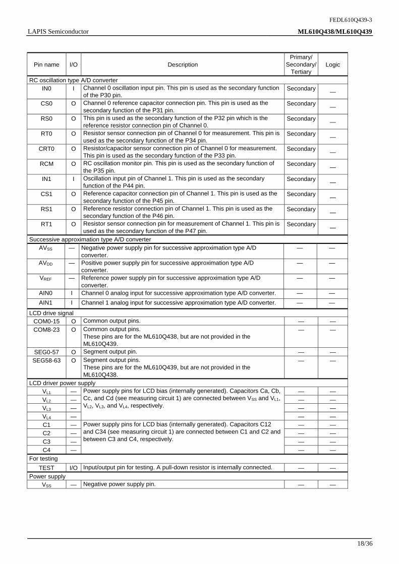
PIN DESCRIPTION
Pin name I/O Description Primary/
Secondary/ Tertiary
Logic
System
RESET_N I Reset input pin. When this pin is set to a “L” level, system reset mode is set and the internal section is initialized. When this pin is set to a “H” level subsequently, program execution starts. A pull-up resistor is internally connected.
— Negative
XT0 I — — XT1 O
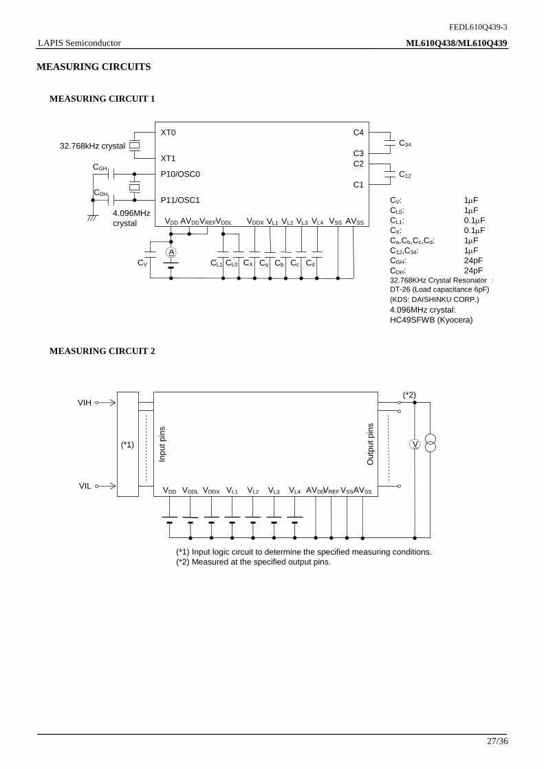
Crystal connection pin for low-speed clock. A 32.768 kHz crystal oscillator (see measuring circuit 1) is connected to this pin. Capacitors CDL and CGL are connected across this pin and VSS as required.
— —
OSC0 I Secondary —
OSC1 O
Crystal/ceramic connection pin for high-speed clock. A crystal or ceramic is connected to this pin (4.1 MHz max.). Capacitors CDH and CGH (see measuring circuit 1) are connected across this pin and VSS. This pin is used as the secondary function of the P10 pin(OSC0) and P11 pin(OSC1).
Secondary —
LSCLK O Low-speed clock output pin. This pin is used as the secondary function of the P20 pin.
Secondary —
OUTCLK O High-speed clock output pin. This pin is used as the secondary function of the P21 pin.
Secondary —
General-purpose input port
P00-P07
I General-purpose input port. Since these pins have secondary functions, the pins cannot be used as a port when the secondary functions are used.
Primary Positive
P10-P11 I General-purpose input port. Since these pins have secondary functions, the pins cannot be used as a port when the secondary functions are used.
Primary Positive
General-purpose output port P20-P22 O General-purpose output port.
Since these pins have secondary functions, the pins cannot be used as a port when the secondary functions are used.
Primary Positive
General-purpose input/output port P30-P35 I/O General-purpose input/output port.
Since these pins have secondary functions, the pins cannot be used as a port when the secondary functions are used.
Primary Positive
P40-P47 I/O General-purpose input/output port. Since these pins have secondary functions, the pins cannot be used as a port when the secondary functions are used.
Primary Positive
PA0-PA5 I/O General-purpose input/output port.
Primary Positive
UART TXD0 O UART data output pin. This pin is used as the secondary function of the
P43 pin. Secondary Positive
RXD0 I UART data input pin. This pin is used as the secondary function of the P42 or the primary function of the P02 pin.
Primary/Secondary
Positive

FEDL610Q439-3
LAPIS Semiconductor ML610Q438/ML610Q439
17/36
Pin name I/O Description Primary/
Secondary/ Tertiary
Logic
I2C bus interface SDA I/O I2C data input/output pin. This pin is used as the secondary function of the
P40 pin. This pin has an NMOS open drain output. When using this pin as a function of the I2C, externally connect a pull-up resistor.
Secondary Positive
SCL O I2C clock output pin. This pin is used as the secondary function of the P41 pin. This pin has an NMOS open drain output. When using this pin as a function of the I2C, externally connect a pull-up resistor.
Secondary Positive
Synchronous serial (SSIO)
SCK0 I/O Synchronous serial clock input/output pin. This pin is used as the tertiary function of the P41 or P45 pin.
Tertiary —
SIN0 I Synchronous serial data input pin. This pin is used as the tertiary function of the P40 or P44 pin.
Tertiary Positive
SOUT0 O Synchronous serial data output pin. This pin is used as the tertiary function of the P42 or P46 pin.
Tertiary Positive
PWM PWM0 O PWM0 output pin. This pin is used as the tertiary function of the P43 or
P34 pin. Tertiary Positive
T0P0CK I PWM0 external clock input pin. This pin is used as the primary function of the P44 pin.
Primary —
PWM1 O PWM1 output pin. This pin is used as the tertiary function of the P47 or P35 pin.
Tertiary Positive
T1P1CK I PWM1 external clock input pin. This pin is used as the primary function of the P45 pin.
Primary —
PWM2 O PWM2 output pin. This pin is used as the tertiary function of the P20 or P30 pin.
Tertiary Positive
P2CK I PWM2 external clock input pin. This pin is used as the primary function of the P02 pin.
Primary —
External interrupt NMI I External non-maskable interrupt input pin. An interrupt is generated on
both edges. Primary Positive/
negativeEXI0-7 I External maskable interrupt input pins. Interrupt enable and edge
selection can be performed for each bit by software. These pins are used as the primary functions of the P00-P07 pins.
Primary Positive/negative
Capture
CAP0 I Primary Positive/negative
CAP1 I
Capture trigger input pins. The value of the time base counter is captured in the register synchronously with the interrupt edge selected by software.These pins are used as the primary functions of the P00 pin(CAP0) and P01 pin(CAP1).
Primary Positive/negative
Timer
T0P0CK I External clock input pin used for Timer 0. This pin is used as the primary function of the P44 pin.
Primary —
T1P1CK I External clock input pin used for Timer 1. This pin is used as the primary function of the P45 pin.
Primary —
Melody MD0 O Melody/buzzer signal output pin. This pin is used as the secondary
function of the P22 pin. Secondary Positive/
negative
LED drive LED0-2 O Nch open drain output pins to drive LED. Primary Positive/
negative
FEDL610Q439-3
LAPIS Semiconductor ML610Q438/ML610Q439
18/36
Pin name I/O Description Primary/
Secondary/ Tertiary
Logic
RC oscillation type A/D converter IN0 I Channel 0 oscillation input pin. This pin is used as the secondary function
of the P30 pin. Secondary
—
CS0 O Channel 0 reference capacitor connection pin. This pin is used as the secondary function of the P31 pin.
Secondary —
RS0 O This pin is used as the secondary function of the P32 pin which is the reference resistor connection pin of Channel 0.
Secondary —
RT0 O Resistor sensor connection pin of Channel 0 for measurement. This pin is used as the secondary function of the P34 pin.
Secondary —
CRT0 O Resistor/capacitor sensor connection pin of Channel 0 for measurement. This pin is used as the secondary function of the P33 pin.
Secondary —
RCM O RC oscillation monitor pin. This pin is used as the secondary function of the P35 pin.
Secondary —
IN1 I Oscillation input pin of Channel 1. This pin is used as the secondary function of the P44 pin.
Secondary —
CS1 O Reference capacitor connection pin of Channel 1. This pin is used as the secondary function of the P45 pin.
Secondary —
RS1 O Reference resistor connection pin of Channel 1. This pin is used as the secondary function of the P46 pin.
Secondary —
RT1 O Resistor sensor connection pin for measurement of Channel 1. This pin is used as the secondary function of the P47 pin.
Secondary —
Successive approximation type A/D converter AVSS — Negative power supply pin for successive approximation type A/D
converter. — —
AVDD — Positive power supply pin for successive approximation type A/D converter.
— —
VREF — Reference power supply pin for successive approximation type A/D converter.
— —
AIN0 I Channel 0 analog input for successive approximation type A/D converter. — —
AIN1 I Channel 1 analog input for successive approximation type A/D converter. — —
LCD drive signal COM0-15 O Common output pins. — — COM8-23 O Common output pins.
These pins are for the ML610Q438, but are not provided in the ML610Q439.
— —
SEG0-57 O Segment output pin. — — SEG58-63 O Segment output pins.
These pins are for the ML610Q439, but are not provided in the ML610Q438.
— —
LCD driver power supply VL1 — — — VL2 — — — VL3 — — — VL4 —
Power supply pins for LCD bias (internally generated). Capacitors Ca, Cb, Cc, and Cd (see measuring circuit 1) are connected between VSS and VL1, VL2, VL3, and VL4, respectively.
— — C1 — — — C2 — — —
C3 — — — C4 —
Power supply pins for LCD bias (internally generated). Capacitors C12 and C34 (see measuring circuit 1) are connected between C1 and C2 and between C3 and C4, respectively.
— —
For testing
TEST I/O Input/output pin for testing. A pull-down resistor is internally connected. — —
Power supply VSS — Negative power supply pin. — —

FEDL610Q439-3
LAPIS Semiconductor ML610Q438/ML610Q439
19/36
VDD — Positive power supply pin. — — VDDL — Positive power supply pin (internally generated) for internal logic.
Capacitors CL0 and CL1 (see measuring circuit 1) are connected between this pin and VSS.
— —
VDDX — Plus-side power supply pin (internally generated) for low-speed oscillation. Capacitor Cx (see measuring circuit 1) is connected between this pin and VSS.
— —
VPP — Power supply pin for programming Flash ROM. A pull-up resistor is internally connected.
— —

FEDL610Q439-3
LAPIS Semiconductor ML610Q438/ML610Q439
20/36
TERMINATION OF UNUSED PINS Table 3 shows methods of terminating the unused pins.
Table 3 Termination of Unused Pins
Pin Recommended pin termination
VPP Open
AVDD VSS
AVSS VSS
VREF VSS
AIN0, AIN1 Open
VL1, VL2, VL3, VL4 Open
C1, C2, C3, C4 Open
RESET_N Open
TEST Open
NMI Open
P00 to P07 VDD or VSS
P10 to P11 VDD
P20 to P22 Open
P30 to P35 Open
P40 to P47 Open
PA0 to PA5 Open
COM0 to 23 Open
SEG0 to 63 Open Note: It is recommended to set the unused input ports and input/output ports to the inputs with pull-down resistors/pull-up resistors or the output mode since the supply current may become excessively large if the pins are left open in the high impedance input setting. The main difference points of ML610Q438 and ML610Q439
Table 4 The main difference points of ML610Q438 and ML610Q439.
Function ML610Q438 ML610Q439
LCD COM COM23 to COM0 COM15 to COM0 LCD SEG SEG55 to SEG0 SEG63 to SEG0

FEDL610Q439-3
LAPIS Semiconductor ML610Q438/ML610Q439
21/36
ELECTRICAL CHARACTERISTICS ABSOLUTE MAXIMUM RATINGS
(VSS = AVSS = 0V)
Parameter Symbol Condition Rating Unit
Power supply voltage 1 VDD Ta = 25C 0.3 to +4.6 V
Power supply voltage 2 AVDD Ta = 25C 0.3 to +4.6 V
Power supply voltage 3 VPP Ta = 25C 0.3 to +9.5 V
Power supply voltage 4 VDDL Ta = 25C 0.3 to +3.6 V
Power supply voltage 5 VDDX Ta = 25C 0.3 to +3.6 V
Power supply voltage 6 VL1 Ta = 25C 0.3 to +1.75 V
Power supply voltage 7 VL2 Ta = 25C 0.3 to +3.5 V
Power supply voltage 8 VL3 Ta = 25C 0.3 to +5.25 V
Power supply voltage 9 VL4 Ta = 25C 0.3 to +7.0 V
Input voltage VIN Ta = 25C 0.3 to VDD+0.3 V
Output voltage VOUT Ta = 25C 0.3 to VDD+0.3 V
Output current 1 IOUT1 Port3–A, Ta = 25C 12 to +11 mA
Output current 2 IOUT2 Port2, Ta = 25C 12 to +20 mA
Power dissipation PD Ta = 25C 122 mW
Storage temperature TSTG 55 to +150 C
RECOMMENDED OPERATING CONDITIONS
(VSS = AVSS = 0V)
Parameter Symbol Condition Range Unit
ML610Q438/Q439 20 to +70 C Operating temperature TOP
ML610Q438P/Q439P
VDD 1.1 to 3.6 V Operating voltage
AVDD 2.2 to 3.6 AVDD
VDD = 1.1 to 3.6V 30k to 36k VDD = 1.3 to 3.6V 30k to 650k Operating frequency (CPU) fOP
VDD = 1.8 to 3.6V 30k to 4.2M
Hz
Low-speed crystal oscillation frequency
fXTL 32.768k Hz
CDL 0 to 12 Low-speed crystal oscillation external capacitor CGL 0 to 12
pF
High-speed crystal/ceramic oscillation frequency
fXTH 4.0M / 4.096M Hz
CDH 24 High-speed crystal oscillation external capacitor CGH 24
pF
CL0 1.030% Capacitor externally connected to VDDL pin CL1 0.130%
F
Capacitor externally connected to VDDX pin
CX 0.130% F
Capacitors externally connected to VL1, 2, 3, 4 pins
Ca, b, c, d 1.030% F
Capacitors externally connected across C1 and C2 pins and across C3 and C4 pins
C12, C34 1.030% F

FEDL610Q439-3
LAPIS Semiconductor ML610Q438/ML610Q439
22/36
OPERATING CONDITIONS OF FLASH ROM
(VSS = AVSS = 0V)
Parameter Symbol Condition Range Unit
Operating temperature TOP At write/erase 0 to +40 C VDD At write/erase*1 2.75 to 3.6
VDDL At write/erase*1 2.5 to 2.75 Operating voltage
VPP At write/erase*1 7.7 to 8.3
V
Write cycles CEP 80 cycles Data retention YDR 10 years
*1: In addition the power supply to VDD pin and VPP pin, within the range 2.5V to 2.75V has to be supplied to VDDL pin when programming and eraseing Flash ROM. DC CHARACTERISTICS (1/5)
(VDD = 1.1 to 3.6V, AVDD = 2.2 to 3.6V, VSS = AVSS = 0V, Ta = 20 to +70C, Ta = 40 to +85C for P version,unless otherwise specified ) (1/5)
Rating Parameter Symbol Condition
Min. Typ. Max. Unit
Measuring circuit
Ta = 25C Typ. 10%
500 Typ. 10%
kHz 500kHz RC oscillation frequency fRC
VDD = 1.3 to 3.6V Ta = 20 to
+70C Typ. 25%
500 Typ. 25%
kHz
PLL oscillation frequency*4 fPLL LSCLK = 32.768kHz
VDD = 1.8 to 3.6V -2.5% 8.192 +2.5% MHz
Low-speed crystal oscillation start time*2
TXTL 0.3 2 s
500kHz RC oscillation start time TRC 50 500 s High-speed crystal oscillation start time*3
TXTH VDD = 1.8 to 3.6V ― 2 20
PLL oscillation start time TPLL VDD = 1.8 to 3.6V ― 1 10 Low-speed oscillation stop detect time*1
TSTOP 0.2 3 20
ms
Reset pulse width PRST 200 Reset noise elimination pulse width
PNRST 0.3 s
Power-on reset activation power rise time
TPOR 10 ms
1
*1: When low-speed crystal oscillation stops for a duration more than the low-speed oscillation stop detect time, the system is reset to shift to system reset mode.
*2 : Use 32.768KHz Crystal Resonator DT-26 (Load capacitance 6pF) (KDS: DAISHINKU CORP.) *3 : Use 4.096MHz Crystal Oscillator CHC49SFWB (Kyocera). *4 : 1024 clock average.
RESET
RESET_N
RESET_N pin reset
VDD
0.9xVDD
0.1xVDD
TPOR
Power on reset
PRST
VIL1 VIL1

FEDL610Q439-3
LAPIS Semiconductor ML610Q438/ML610Q439
23/36
DC CHARACTERISTICS (2/5)
(VDD = 1.1 to 3.6V, AVDD = 2.2 to 3.6V, VSS = AVSS = 0V, Ta = 20 to +70C, Ta = 40 to +85C for P version, unless otherwise specified) (2/5)
Rating Parameter Symbol Condition
Min. Typ. Max. Unit
Measuring circuit
CN4–0 = 00H 0.89 0.94 0.99
CN4–0 = 01H 0.91 0.96 1.01
CN4–0 = 02H 0.93 0.98 1.03
CN4–0 = 03H 0.95 1.00 1.05
CN4–0 = 04H 0.97 1.02 1.07
CN4–0 = 05H 0.99 1.04 1.09
CN4–0 = 06H 1.01 1.06 1.11
CN4–0 = 07H 1.03 1.08 1.13
CN4–0 = 08H 1.05 1.10 1.15
CN4–0 = 09H 1.07 1.12 1.17
CN4–0 = 0AH 1.09 1.14 1.19
CN4–0 = 0BH 1.11 1.16 1.21
CN4–0 = 0CH 1.13 1.18 1.23
CN4–0 = 0DH 1.15 1.20 1.25
CN4–0 = 0EH 1.17 1.22 1.27
CN4–0 = 0FH 1.19 1.24 1.29
CN4–0 = 10H 1.21 1.26 1.31
CN4–0 = 11H 1.23 1.28 1.33
CN4–0 = 12H 1.25 1.30 1.35
CN4–0 = 13H 1.27 1.32 1.37
CN4–0 = 14H *1 1.29 1.34 1.39
CN4–0 = 15H *1 1.31 1.36 1.41
CN4–0 = 16H *1 1.33 1.38 1.43
CN4–0 = 17H *1 1.35 1.40 1.45
CN4–0 = 18H *1 1.37 1.42 1.47
CN4–0 = 19H *1 1.39 1.44 1.49
CN4–0 = 1AH *1 1.41 1.46 1.51
CN4–0 = 1BH *1 1.43 1.48 1.53
CN4–0 = 1CH *1 1.45 1.50 1.55
CN4–0 = 1DH *1 1.47 1.52 1.57
CN4–0 = 1EH *1 1.49 1.54 1.59
VL1 voltage VL1 VDD = 3.0V, Tj = 25C
CN4–0 = 1FH *1 1.51 1.56 1.61
V
VL1 temperature deviation VL1 VDD = 3.0V mV/C
VL1 voltage dependency
VL1 VDD = 1.3 to 3.6V 5 20 mV/V
VL2 voltage VL2 VDD = 3.0V, Tj = 25C 300k load (VL4VSS)
Typ. %
VL12Typ. +4%
1/3 bias VL12VL3 voltage VL3
1/4 bias
Typ. 10% VL13
Typ. +4%
1/3 bias VL13VL4 voltage VL4
VDD = 3.0V, Tj = 25C
300k load (VL4VSS) 1/4 bias
Typ. 10% VL14
Typ. +5%
V
LCD bias voltage generation time
TBIAS 600 ms
1
*1: When using 1/4 bias, the VL1 voltage is set to typ. 1.32 V (same voltage as in CN4–0 = 13H).

FEDL610Q439-3
LAPIS Semiconductor ML610Q438/ML610Q439
24/36
DC CHARACTERISTICS (3/5)
(VDD = 1.1 to 3.6V, AVDD = 2.2 to 3.6V, VSS = AVSS = 0V, Ta = 20 to +70C, Ta = 40 to +85C for P version,unless otherwise specified) (3/5)
Rating Parameter Symbol Condition
Min. Typ. Max. Unit
Measuringcircuit
LD2–0 = 0H 1.35
LD2–0 = 1H 1.4
LD2–0 = 2H 1.45
LD2–0 = 3H 1.5
LD2–0 = 4H 1.6
LD2–0 = 5H 1.7
LD2–0 = 6H 1.8
LD2–0 = 7H 1.9
LD2–0 = 8H 2.0
LD2–0 = 9H 2.1
LD2–0 = 0AH 2.2
LD2–0 = 0BH 2.3
LD2–0 = 0CH 2.4
LD2–0 = 0DH 2.5
LD2–0 = 0EH 2.7
BLD threshold voltage
VBLD VDD = 1.35 to 3.6V
LD2–0 = 0FH
Typ. 2%
2.9
Typ. +2%
V
BLD threshold voltage temperature deviation
VBLD VDD = 1.35 to 3.6V 0 %/C
Ta = 25C
0.15 0.50 Supply current 1
IDD1 CPU: In STOP state. Low-speed/high-speed oscillation: stopped. Ta = -20
to +70C 2.50
A
Ta = 25C
0.5 1.3 Supply current 2
IDD2
CPU: In HALT state (LTBC, RTC: Operating*3*5). High-speed oscillation: Stopped. LCD/BIAS circuits: Stopped.
Ta = -20 to +70C
3.5 A
Ta = 25C
5 7 Supply current 3
IDD3 CPU: In 32.768kHz operating state.*1*3
High-speed oscillation: Stopped. LCD/BIAS circuits: Operating.*2 Ta = -20
to +70C 12
A
Ta = 25C
70 85 Supply current 4
IDD4 CPU: In 500kHz CR operating state. LCD/BIAS circuits: Operating.*2*3 Ta = -20
to +70C 100 A
1
Ta = 25C
0.8 1.0 Supply current 5
IDD5
CPU: In 4.096MHz operating state. PLL: In oscillating state. LCD/BIAS circuits: Operating. *2*3 VDD = 1.8 to 3.6V
Ta = -20 to +70C
1.2
mA
*1 : CPU operating rate is 100% (No HALT state). *2 : All SEGs: off waveform, No LCD panel load, 1/3 bias, 1/3 duty, Frame frequency: Approx. 64 Hz, Bias voltage multiplying clock: 1/128 LSCLK (256Hz) *3 : Use 32.768KHz Crystal Resonator DT-26 (Load capacitance 6pF) (KDS: DAISHINKU CORP.) *4 : Use 4.096MHz Crystal Oscillator CHC49SFWB (Kyocera). *5 : Significant bits of BLKCON0~BLKCON4 registers are all “1”.

FEDL610Q439-3
LAPIS Semiconductor ML610Q438/ML610Q439
25/36
DC CHARACTERISTICS (4/5)
(VDD = 1.1 to 3.6V, AVDD = 2.2 to 3.6V, VSS = AVSS = 0V, Ta = 20 to +70C, Ta = 40 to +85C for P version,unless otherwise specified) (4/5)
Rating Parameter Symbol Condition
Min. Typ. Max. Unit
Measuring circuit
IOH1 = 0.5mA, VDD = 1.8 to 3.6V VDD
0.5
IOH1 = -0.1mA, VDD = 1.3 to 3.6V VDD
0.3 VOH1
IOH1 = -0.03mA, VDD = 1.1 to 3.6V VDD
0.3
IOL1 = +0.5mA, VDD = 1.8 to 3.6V 0.5
IOL1 = +0.1mA, VDD = 1.3 to 3.6V 0.5
Output voltage 1 (P20–P22/2nd function is selected) (P30–P36) (P40–P47) (PA0–PA5) VOL1
IOL1 = +0.03mA, VDD = 1.1 to 3.6V 0.3
IOH1 = 0.5mA, VDD = 1.8 to 3.6V VDD
0.5
IOH1 = -0.1mA, VDD = 1.3 to 3.6V VDD
0.3 VOH2
IOH1 = -0.03mA, VDD = 1.1 to 3.6V VDD
0.3
Output voltage 2 (P20–P22/2nd function is Not selected)
VOL2 IOL2 = +5mA, VDD = 1.8 to 3.6V 0.5
Output voltage 3 (P40–P41)
VOL3 IOL3 = +3mA, VDD = 2.0 to 3.6V
(when I2C mode is selected) 0.4
VOH4 IOH4 = 0.2mA, VL1=1.2V VL4
0.2
VOMH4 IOMH4 = +0.2mA, VL1=1.2V VL3
+0.2
VOMH4S IOMH4S = 0.2mA, VL1=1.2V VL3
0.2
VOM4 IOM4 = +0.2mA, VL1=1.2V VL2
+0.2
VOM4S IOM4S = 0.2mA, VL1=1.2V VL2
0.2
VOML4 IOML4 = +0.2mA, VL1=1.2V VL1
+0.2
VOML4S IOML4S = 0.2mA, VL1=1.2V VL1
0.2
Output voltage 4 (COM0–23) (SEG0–63)
VOL4 IOL4 = +0.2mA, VL1=1.2V 0.2
V 2
IOOH VOH = VDD (in high-impedance state) 1 Output leakage (P20–P22) (P30–P35) (P40–P47) (PA0–PA5)
IOOL VOL = VSS (in high-impedance state) 1
A 3
IIH1 VIH1 = VDD 0 1
VDD = 1.8 to 3.6V 600 300 20
VDD = 1.3 to 3.6V 600 300 -10
Input current 1 (RESET_N) IIL1 VIL1 = VSS
VDD = 1.1 to 3.6V 600 300 -2
VDD = 1.8 to 3.6V 20 300 600
VDD = 1.3 to 3.6V 10 300 600 IIH1 VIH1 = VDD
VDD = 1.1 to 3.6V 2 300 600
Input current 1 (TEST)
IIL1 VIL1 = Vss -1
VDD = 1.8 to 3.6V 2 30 200
VDD = 1.3 to 3.6V 0.2 30 200 IIH2 VIH2 = VDD
(when pulled-down)VDD = 1.1 to 3.6V 0.01 30 200
Input current 2 (NMI) (P00–P03) (P04–P07)
IIL2 VIL2 = VSS VDD = 1.8 to 3.6V 200 30 2
A 4

FEDL610Q439-3
LAPIS Semiconductor ML610Q438/ML610Q439
26/36
VDD = 1.3 to 3.6V 200 30 -0.2 (when pulled-up)
VDD = 1.1 to 3.6V 200 30 -0.01
IIH2Z VIH2 = VDD (in high-impedance state) 1
(P10–P11) (P30–P35) (P40–P47) (PA0–PA5)
IIL2Z VIL2 = VSS (in high-impedance state) 1
DC CHARACTERISTICS (5/5)
(VDD = 1.1 to 3.6V, AVDD = 2.2 to 3.6V, VSS = AVSS = 0V, Ta = 20 to +70C, Ta = 40 to +85C for P version,unless otherwise specified) (5/5)
Rating Parameter Symbol Condition
Min. Typ. Max. Unit
Measuring circuit
VDD = 1.3 to 3.6V0.7 VDD
VDD
VIH1
VDD = 1.1 to 3.6V0.7 VDD
VDD
VDD = 1.3 to 3.6V 0 0.3 VDD
Input voltage 1 (RESET_N) (TEST) (NMI) (P00–P03) (P04–P07) (P10–P11) (P31–P35) (P40–P43) (P45–P47) (PA0–PA5)
VIL1
VDD = 1.1 to 3.6V 0 0.2 VDD
VDD = 2.0 to 3.6V 0.05 VDD
0.18 VDD
0.4 VDD
Hysteresis width (RESET_N) (TEST) (NMI) (P00–P03) (P04–P07) (P10–P11) (P31–P35) (P40–P43) (P45–P47) (PA0–PA5)
VT
VDD = 1.1 to 3.6V 0.02 VDD
0.18 VDD
0.4 VDD
VIH2 0.7 VDD
VDD Input voltage 2 (P30, P44)
VIL2 0 0.3 VDD
V 5
Input pin capacitance (NMI) (P00–P03) (P04–P07) (P10–P11) (P30–P35) (P40–P47) (PA0–PA5)
CIN f = 10kHz
Vrms = 50mV Ta = 25C
5 pF
HYSTERESIS WIDTH
VT Input signal
Internal signal
VDD
VSS
VSS
VDDL
FEDL610Q439-3
LAPIS Semiconductor ML610Q438/ML610Q439
27/36
MEASURING CIRCUITS
MEASURING CIRCUIT 1
MEASURING CIRCUIT 2
XT0
XT1
P10/OSC0
P11/OSC1
32.768kHz crystal
4.096MHz crystal
CGH
CDH
A
VDD AVDD VREF VDDL VDDX
CL1 CL0 CX
VL1
Ca
VL2
Cb
VL3
Cc
VL4
Cd
VSS AVSS
C4
C3C2
C1C12
C34
CV: 1F CL0: 1F CL1: 0.1F CX: 0.1F Ca,Cb,Cc,Cd: 1F C12,C34: 1F CGH: 24pF CDH: 24pF 32.768KHz Crystal Resonator : DT-26 (Load capacitance 6pF) (KDS: DAISHINKU CORP.) 4.096MHz crystal: HC49SFWB (Kyocera)
CV
Inp
ut p
ins
V
VDD AVDDVREFVDDL VDDX VL1 VL2 VL3 VL4 VSSAVSS
VIH
VIL
Ou
tpu
t pi
ns
(*1) Input logic circuit to determine the specified measuring conditions. (*2) Measured at the specified output pins.
(*2)
(*1)

FEDL610Q439-3
LAPIS Semiconductor ML610Q438/ML610Q439
28/36
MEASURING CIRCUIT 3
MEASURING CIRCUIT 4
MEASURING CIRCUIT 5
Inp
ut p
ins
A
VDD AVDDVREFVDDL VDDX VL1 VL2 VL3 VL4 VSSAVSS
VIH
VIL
Ou
tpu
t pi
ns
*1: Input logic circuit to determine the specified measuring conditions. *2: Measured at the specified output pins.
(*2)
RS1 In
pu
t pin
s
A
VDD AVDDVREFVDDL VDDX VL1 VL2 VL3 VL4 VSSAVSS
Ou
tpu
t pi
ns
*3: Measured at the specified output pins.
(*3)
Inp
ut p
ins
VDD AVDDVREFVDDL VDDX VL1 VL2 VL3 VL4 VSSAVSS
VIH
VIL
Ou
tpu
t pi
ns
*1: Input logic circuit to determine the specified measuring conditions.
(*1)
Wa
vefo
rm m
onito
ring

FEDL610Q439-3
LAPIS Semiconductor ML610Q438/ML610Q439
29/36
AC CHARACTERISTICS (External Interrupt) (VDD = 1.1 to 3.6V, AVDD = 2.2 to 3.6V, VSS = AVSS = 0V, Ta = 20 to +70C, Ta = 40 to +85C for P version,
unless otherwise specified)
Rating Parameter Symbol Condition
Min. Typ. Max.Unit
External interrupt disable period TNUL Interrupt: Enabled (MIE = 1),
CPU: NOP operation
System clock: 32.768kHz 76.8 106.8 s
AC CHARACTERISTICS (UART)
(VDD = 1.1 to 3.6V, AVDD = 2.2 to 3.6V, VSS = AVSS = 0V, Ta = 20 to +70C, Ta = 40 to +85C for P version, unless otherwise specified)
Rating Parameter Symbol Condition
Min. Typ. Max. Unit
Transmit baud rate tTBRT BRT*1 s
Receive baud rate tRBRT BRT*1 3%
BRT*1 BRT*1 +3%
s
*1: Baud rate period (including the error of the clock frequency selected) set with the UART baud rate register (UA0BRTL,H) and the UART mode register 0 (UA0MOD0).
tRBRT
TXD0*
RXD0*
*: Indicates the secondary function of the port.
tTBRT
tNUL
P00–P07
(Rising-edge interrupt)
P00–P07
(Falling-edge interrupt)
NMI, P00–P07
(Both-edge interrupt) tNUL
tNUL

FEDL610Q439-3
LAPIS Semiconductor ML610Q438/ML610Q439
30/36
AC CHARACTERISTICS (Synchronous Serial Port)
(VDD = 1.1 to 3.6V, AVDD = 2.2 to 3.6V, VSS = AVSS = 0V, Ta = 20 to +70C, Ta = 40 to +85C for P version,unless otherwise specified)
Rating Parameter Symbol Condition
Min. Typ. Max. Unit
When high-speed oscillation is not active
10 s SCLK input cycle (slave mode)
tSCYC When high-speed oscillation is
active (VDD = 1.8 to 3.6V) 1 s
SCLK output cycle (master mode)
tSCYC SCLK*1 s
When high-speed oscillation is not active
4 s SCLK input pulse width (slave mode)
tSW When high-speed oscillation is
active (VDD = 1.8 to 3.6V) 0.4 s
SCLK output pulse width (master mode)
tSW SCLK*1
0.4 SCLK*1 0.5
SCLK*1
0.6 s
SOUT output delay time (slave mode)
tSD 180 ns
SOUT output delay time (master mode)
tSD 80 ns
SIN input setup time (slave mode)
tSS 80 ns
SIN input setup time (master mode)
tSS 180 ns
SIN input hold time
tSH 80 ns
*1: Clock period selected with S0CK3–0 of the serial port 0 mode register (SIO0MOD1)
tSD
SCLK0*
SIN0*
SOUT0*
*: Indicates the secondary function of the port.
tSD
tSS tSH
tSW tSW
tSCYC
FEDL610Q439-3
LAPIS Semiconductor ML610Q438/ML610Q439
31/36
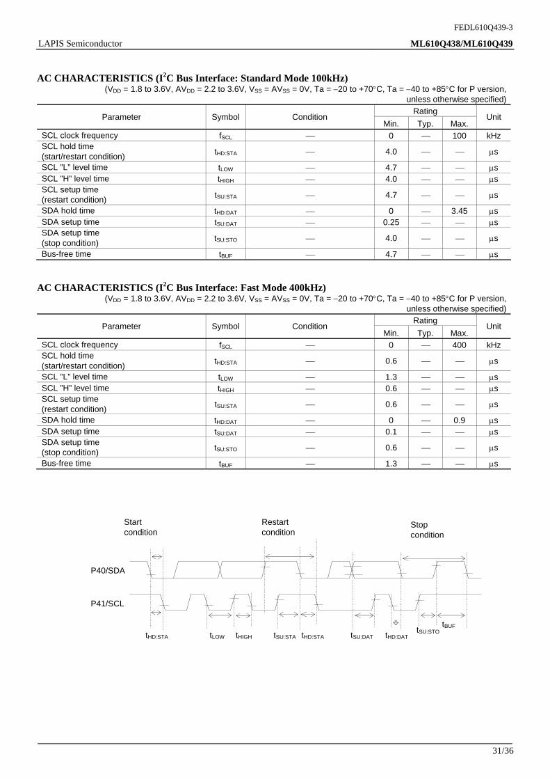
AC CHARACTERISTICS (I2C Bus Interface: Standard Mode 100kHz)
(VDD = 1.8 to 3.6V, AVDD = 2.2 to 3.6V, VSS = AVSS = 0V, Ta = 20 to +70C, Ta = 40 to +85C for P version,unless otherwise specified)
Rating Parameter Symbol Condition
Min. Typ. Max.Unit
SCL clock frequency fSCL 0 100 kHz SCL hold time (start/restart condition)
tHD:STA 4.0 s
SCL ”L” level time tLOW 4.7 s SCL ”H” level time tHIGH 4.0 s SCL setup time (restart condition)
tSU:STA 4.7 s
SDA hold time tHD:DAT 0 3.45 s SDA setup time tSU:DAT 0.25 s SDA setup time (stop condition)
tSU:STO 4.0 s
Bus-free time tBUF 4.7 s
AC CHARACTERISTICS (I2C Bus Interface: Fast Mode 400kHz)
(VDD = 1.8 to 3.6V, AVDD = 2.2 to 3.6V, VSS = AVSS = 0V, Ta = 20 to +70C, Ta = 40 to +85C for P version,unless otherwise specified)
Rating Parameter Symbol Condition
Min. Typ. Max.Unit
SCL clock frequency fSCL 0 400 kHz SCL hold time (start/restart condition)
tHD:STA 0.6 s
SCL ”L” level time tLOW 1.3 s SCL ”H” level time tHIGH 0.6 s SCL setup time (restart condition)
tSU:STA 0.6 s
SDA hold time tHD:DAT 0 0.9 s SDA setup time tSU:DAT 0.1 s SDA setup time (stop condition)
tSU:STO 0.6 s
Bus-free time tBUF 1.3 s
P41/SCL
P40/SDA
Start condition
Restart condition
Stop condition
tBUF tHD:STA tLOW tHIGH tSU:STA tHD:STA tSU:DAT tHD:DAT
tSU:STO

FEDL610Q439-3
LAPIS Semiconductor ML610Q438/ML610Q439
32/36
AC CHARACTERISTICS (RC Oscillation A/D Converter) (VDD = 1.3 to 3.6V, AVDD = 2.2 to 3.6V, VSS = AVSS = 0V, Ta = 20 to +70C, Ta = 40 to +85C for P version,
unless otherwise specified)
Rating Parameter Symbol Condition
Min. Typ. Max. Unit
Resistors for oscillation RS0, RS1,
RT0, RT0-1,RT1
CS0, CT0, CS1 740pF 1 k
fOSC1 Resistor for oscillation = 1k 209.4 330.6 435.1 kHz fOSC2 Resistor for oscillation = 10k 41.29 55.27 64.16 kHz
Oscillation frequency VDD = 1.5V
fOSC3 Resistor for oscillation = 100k 4.71 5.97 7.06 kHz Kf1 RT0, RT0-1, RT1 = 1kHz 5.567 5.982 6.225 Kf2 RT0, RT0-1, RT1 = 10 kHz 0.99 1 1.01
RS to RT oscillation frequency ratio *1
VDD = 1.5V Kf3 RT0, RT0-1, RT1 = 100 kHz 0.104 0.108 0.118 fOSC1 Resistor for oscillation = 1k 407.3 486.7 594.6 kHzfOSC2 Resistor for oscillation = 10k 49.76 59.28 72.76 kHz
Oscillation frequency VDD = 3.0V
fOSC3 Resistor for oscillation = 100k 5.04 5.993 7.04 kHzKf1 RT0, RT0-1, RT1 = 1kHz 8.006 8.210 8.416 Kf2 RT0, RT0-1, RT1 = 10 kHz 0.99 1 1.01
RS to RT oscillation frequency ratio *1
VDD = 3.0V Kf3 RT0, RT0-1, RT1 = 100 kHz 0.100 0.108 0.115 *1: Kfx is the ratio of the oscillation frequency by the sensor resistor to the oscillation frequency by the reference resistor on the same
conditions.
fOSCX(RT0CS0 oscillation) fOSCX(RT0-1CS0 oscillation) fOSCX(RT1CS1 oscillation)
Kfx = fOSCX(RS0CS0 oscillation) , fOSCX(RS0CS0 oscillation) , fOSCX(RS1CS1 oscillation)
(x = 1, 2, 3) Note:
- Please have the shortest layout for the common node (wiring patterns which are connected to the external capacitors, resistors and IN0/IN1 pin), including CVR0/CVR1. Especially, do not have long wire between IN0/IN1 and RS0/RS1. The coupling capacitance on the wires may occur incorrect A/D conversion. Also, please do not have signals which may be a source of noise around the node.
- When RT0/RT1 (Thermistor and etc.) requires long wiring due to the restricted placement, please have VSS(GND) trace next to the signal.
- Please make wiring to components (capacitor, resisteor and etc.) necessory for objective measurement. Wiring to reserved components may affect to the A/D conversion operation by noise the components itself may have.
VDD VDDL VDDX
CL1 CL0 CX
VSS
CV
RT0, RT0-1, RT1: 1k /10k/100k RS0, RS1: 10k CS0, CT0, CS1: 560pF CVR0, CVR1: 820pF
RCM Frequency measurement (fOSCX)
Inp
ut p
ins
VIH
VIL
*1: Input logic circuit to determine the specified measuring conditions.
(*1)
CS0 RT0 IN1 CS1 RS1 RT1
CS
0
RS0
RS
0
RCT0
RI0
-1
CT
0
RT
0
CS
1
RS
1
RT
1
IN0
CVR0 CVR1

FEDL610Q439-3
LAPIS Semiconductor ML610Q438/ML610Q439
33/36
Electrical Characteristics of Successive Approximation Type A/D Converter (VDD = 1.8 to 3.6V, AVDD = 2.2 to 3.6V, VSS = AVSS = 0V, Ta = 20 to +70C, Ta = 40 to +85C for P version,
unless otherwise specified)
Rating Parameter Symbol Condition
Min. Typ. Max.Unit
Resolution n 12 bit 2.7V VREF 3.6V 4 +4
Integral non-linearity error IDL 2.2V VREF 2.7V 6 +6 2.7V VREF 3.6V 3 +3
Differential non-linearity error DNL 2.2V VREF 2.7V 5 +5
Zero-scale error VOFF 6 +6 Full-scale error FSE 6 +6
LSB
Reference voltage VREF 2.2 AVDD V SACK = 0
(HSCLK = 375kHz to 625kHz) 25
Conversion time tCONV SACK = 1
(HSCLK = 1.5MHz to 4.2MHz) 112
/CH
: Period of high-speed clock (HSCLK)
A
VDD AVDD
VREF
VDDL
VDDX
VSS
AVSSAnalog input
1F
RI5k 0.1F
0.1F
AIN0,AIN1
10F
0.1F
+
1F
Reference voltage

FEDL610Q439-3
LAPIS Semiconductor ML610Q438/ML610Q439
34/36
Package Dimensions
(Unit: mm)
Notes for Mounting the Surface Mount Type Package The surface mount type packages are very susceptible to heat in reflow mounting and humidity absorbed in storage. Therefore, before you perform reflow mounting, contact our responsible sales person for the product name, package name, pin number, package code and desired mounting conditions (reflow method, temperature and times).

FEDL610Q439-3
LAPIS Semiconductor ML610Q438/ML610Q439
35/36
Revision History
Page Document No. Date Previous
Edition CurrentEdition
Description
FEDL610Q439-01 Aug. 24,2010 – – Formally edition 1.0 FEDL610Q439-02 Feb. 2,2011 34 34 Change of a Package Dimensions FEDL610Q439-03 Jun. 7,2011 3 3 Add the P persion

FEDL610Q439-3
LAPIS Semiconductor ML610Q438/ML610Q439
36/36
NOTICE
No copying or reproduction of this document, in part or in whole, is permitted without the consent of LAPIS Semiconductor Co., Ltd.
The content specified herein is subject to change for improvement without notice.
The content specified herein is for the purpose of introducing LAPIS Semiconductor's products (hereinafter "Products"). If you wish to use any such Product, please be sure to refer to the specifications, which can be obtained from LAPIS Semiconductor upon request.
Examples of application circuits, circuit constants and any other information contained herein illustrate the standard usage and operations of the Products. The peripheral conditions must be taken into account when designing circuits for mass production.
Great care was taken in ensuring the accuracy of the information specified in this document. However, should you incur any damage arising from any inaccuracy or misprint of such information, LAPIS Semiconductor shall bear no responsibility for such damage.
The technical information specified herein is intended only to show the typical functions of and examples of application circuits for the Products. LAPIS Semiconductor does not grant you, explicitly or implicitly, any license to use or exercise intellectual property or other rights held by LAPIS Semiconductor and other parties. LAPIS Semiconductor shall bear no responsibility whatsoever for any dispute arising from the use of such technical information.
The Products specified in this document are intended to be used with general-use electronic equipment or devices (such as audio visual equipment, office-automation equipment, communication devices, electronic appliances and amusement devices).
The Products specified in this document are not designed to be radiation tolerant.
While LAPIS Semiconductor always makes efforts to enhance the quality and reliability of its Products, a Product may fail or malfunction for a variety of reasons.
Please be sure to implement in your equipment using the Products safety measures to guard against the possibility of physical injury, fire or any other damage caused in the event of the failure of any Product, such as derating, redundancy, fire control and fail-safe designs. LAPIS Semiconductor shall bear no responsibility whatsoever for your use of any Product outside of the prescribed scope or not in accordance with the instruction manual.
The Products are not designed or manufactured to be used with any equipment, device or system which requires an extremely high level of reliability the failure or malfunction of which may result in a direct threat to human life or create a risk of human injury (such as a medical instrument, transportation equipment, aerospace machinery, nuclear-reactor controller, fuel-controller or other safety device). LAPIS Semiconductor shall bear no responsibility in any way for use of any of the Products for the above special purposes. If a Product is intended to be used for any such special purpose, please contact a ROHM sales representative before purchasing.
If you intend to export or ship overseas any Product or technology specified herein that may be controlled under the Foreign Exchange and the Foreign Trade Law, you will be required to obtain a license or permit under the Law.
Copyright 2010 - 2011 LAPIS Semiconductor Co., Ltd.

Mouser Electronics
Authorized Distributor
Click to View Pricing, Inventory, Delivery & Lifecycle Information: ROHM Semiconductor:
ML610Q438P-NNNTC0AGL ML610Q439P-NNNTC0AGL ML610Q438P-NNNTC0AAL