mixerless transmitters for wireless communications
TRANSCRIPT

University of Calgary
PRISM: University of Calgary's Digital Repository
Graduate Studies The Vault: Electronic Theses and Dissertations
2014-09-30
Mixerless Transmitters for Wireless Communications
Illath Veetil, Suhas
Illath Veetil, S. (2014). Mixerless Transmitters for Wireless Communications (Unpublished
master's thesis). University of Calgary, Calgary, AB. doi:10.11575/PRISM/26926
http://hdl.handle.net/11023/1887
master thesis
University of Calgary graduate students retain copyright ownership and moral rights for their
thesis. You may use this material in any way that is permitted by the Copyright Act or through
licensing that has been assigned to the document. For uses that are not allowable under
copyright legislation or licensing, you are required to seek permission.
Downloaded from PRISM: https://prism.ucalgary.ca

UNIVERSITY OF CALGARY
Mixerless Transmitters for Wireless Communications
by
Suhas Illath Veetil
A THESIS
SUBMITTED TO THE FACULTY OF GRADUATE STUDIES
IN PARTIAL FULFILMENT OF THE REQUIREMENTS FOR THE
DEGREE OF MASTER OF SCIENCE
GRADUATE PROGRAM IN ELECTRICAL AND COMPUTER ENGINEERING
CALGARY, ALBERTA
SEPTEMBER, 2014
© Suhas Illath Veetil 2014

Abstract
There is immense research in developing digital transmitters that are multi-standard and
reconfigurable. A promising technique is RF Digital to Analog Converter (RFDAC), where the
input digital baseband signal is directly converted to an analog RF signal. The existing RFDAC
based transmitters use mixers and adopt filtering to avoid mixer spurs. Polar transmitters too use
mixers and need filtering. The use of RF filtering in these transmitter topologies limits the
bandwidth and therefore the multi-standard reconfigurability of such transmitters.
This thesis aims to develop mixerless transmitter architectures that are reconfigurable. A
mixerless polar modulator-based transmitter and a mixerless three-way amplitude modulation
based transmitter are proposed for OFDM signals. The proposed architectures translate the
baseband signal to RF without using mixers. The topologies do not have any emissions over a
wide frequency band. The large RF bandwidth and the absence of filters make the designs more
reconfigurable and suitable for integration.
ii

Acknowledgements
I take this opportunity to place on record my deep sense of gratitude to my supervisor, Dr.
Mohamed Helaoui for his guidance, care, patience and illuminating discussions throughout my
work. Without his supervision and constant help through constructive comments, this thesis
would not have been possible.
I am grateful to my professor Dr. Fadhel M. Ghannouchi for providing me an excellent
opportunity to do this work in his research group and providing the best facilities and atmosphere
for the development of this thesis.
I thank my committee members Dr. Reda Alhajj and Dr. Kartikeya Murari for their valuable
comments and advice on the thesis work.
Special thanks to Andrew Kwan and Mohammadhassan Akbarpour, PhD candidates and Dr.
Mehdi Vejdani Amiri, Post-Doctoral Fellow for helping me with their advice regarding
experiments in the lab. I would like to thank Ivana D’Adamo, administrative support staff and
Chris Simon, technical support staff for their help and support. I thank each and every member of
the iRadio Labs for their support and friendship throughout my work.
I remember with gratitude, the cooperation and help given to me by my friends and also for
finding time for the long Badminton games.
I thank my parents, sisters and brothers-in-law for their constant support and motivation
throughout my life.
iii

Dedication
To my friends
iv

Table of Contents
Abstract ........................................................................................................................................... ii
Acknowledgements ........................................................................................................................ iii
Dedication ...................................................................................................................................... iv
Table of Contents ............................................................................................................................ v
List of Tables ................................................................................................................................. ix
List of Figures and Illustrations ...................................................................................................... x
List of Symbols, Abbreviations and Nomenclature ..................................................................... xiii
Introduction .......................................................................................................... 1 Chapter One:
1.1 Radio transmitter fundamentals ........................................................................................ 4
1.2 Transmitter key parameters ............................................................................................... 5
1.2.1 Linearity ..................................................................................................................... 5
1.2.2 Error vector magnitude .............................................................................................. 6
1.2.3 Adjacent channel power ratio .................................................................................... 7
1.3 Digital radio transmitters .................................................................................................. 8
1.3.1 RFDAC fundamentals ................................................................................................ 9
1.3.2 Suppression of RFDAC emissions .......................................................................... 11
1.4 Polar transmitters ............................................................................................................ 15
1.4.1 Envelope and phase signal recombination ............................................................... 16
1.5 Vector modulators ........................................................................................................... 21
1.6 Summary of transmitter architectures ............................................................................. 23
v

1.7 Goals and objectives ....................................................................................................... 24
1.8 Thesis outline .................................................................................................................. 26
1.9 Conclusion ...................................................................................................................... 28
Amplitude Modulation using Variable Gain Amplifier (VGA) ........................ 29 Chapter Two:
2.1 Introduction ..................................................................................................................... 29
2.2 VGA fundamentals ......................................................................................................... 29
2.3 VGA as amplitude modulator ......................................................................................... 31
2.4 VGA imperfections ......................................................................................................... 33
2.5 VGA calibration .............................................................................................................. 34
2.5.1 Memory polynomial calibration .............................................................................. 34
2.5.2 Least squares technique ........................................................................................... 36
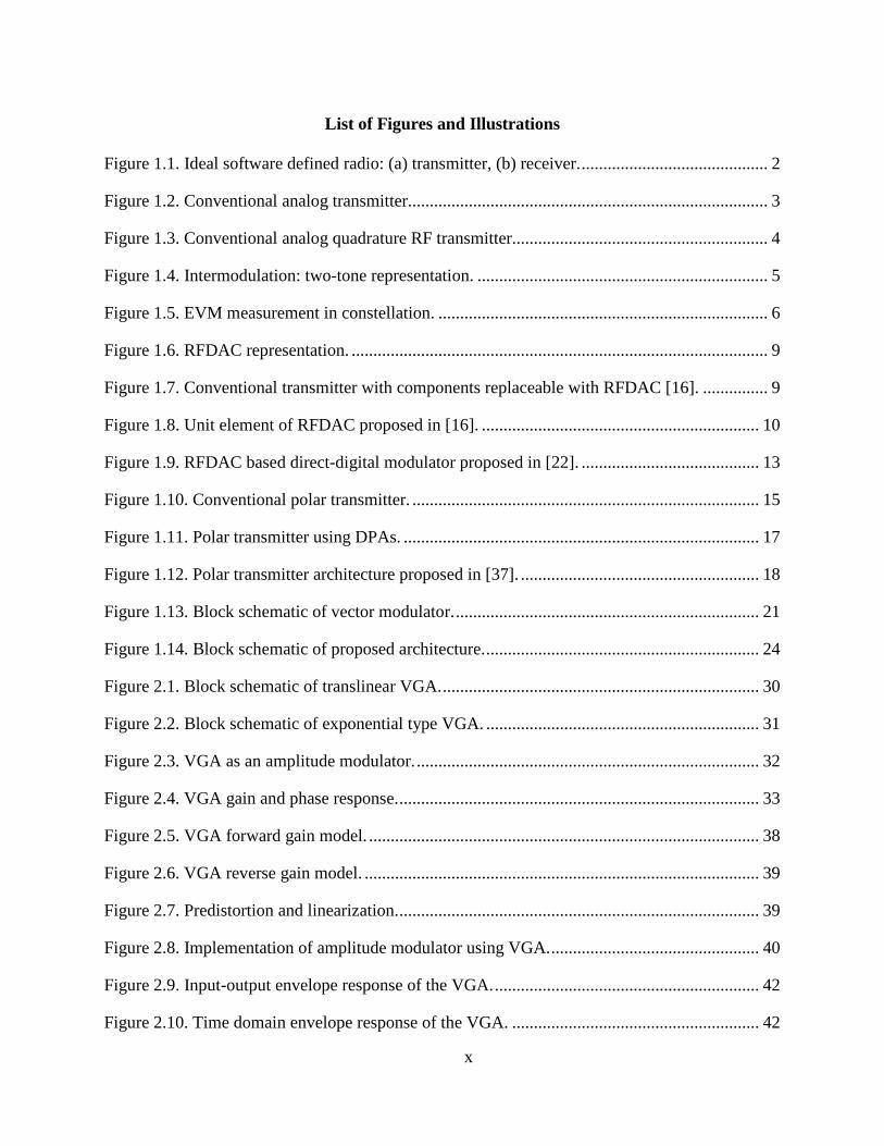
2.5.3 Digital predistortion technique ................................................................................ 38
2.6 Implementation ............................................................................................................... 40
2.7 Measurement results ....................................................................................................... 41
2.8 Conclusion ...................................................................................................................... 44
Phase Modulation using Analog Phase Shifter ................................................ 45 Chapter Three:
3.1 Introduction ..................................................................................................................... 45
3.2 Phase shifter fundamentals.............................................................................................. 46
3.3 Phase shifter as phase modulator .................................................................................... 48
3.4 Phase mapping ................................................................................................................ 50
3.5 Phase conditioning .......................................................................................................... 51
3.5.1 Phase conditioning techniques ................................................................................. 54
3.6 Phase shifter imperfections ............................................................................................. 56
vi

3.7 Phase shifter calibration .................................................................................................. 57
3.7.1 Memory polynomial calibration .............................................................................. 58
3.7.2 Digital predistortion of phase signal ........................................................................ 58
3.8 Phase modulator implementation .................................................................................... 59
3.9 Measurement results ....................................................................................................... 60
3.10 Conclusion .................................................................................................................... 64
Mixerless Polar Modulator-Based Transmitter Architecture ............................ 65 Chapter Four:
4.1 Introduction ..................................................................................................................... 65
4.2 Mixerless polar modulator-based transmitter ................................................................. 65
4.3 VGA gain and phase response ........................................................................................ 66
4.4 Phase shifter gain and phase response ............................................................................ 68
4.5 Calibration of the proposed transmitter architecture ...................................................... 69
4.5.1 Modified memory polynomial calibration ............................................................... 70
4.5.2 Digital predistortion technique ................................................................................ 72
4.6 Transmitter implementation ............................................................................................ 73
4.7 Measurement results ....................................................................................................... 74
4.8 Constellation shift compensation .................................................................................... 81
4.9 Conclusion ...................................................................................................................... 85
Three-way Amplitude Modulation-Based Transmitter Architecture ................. 86 Chapter Five:
5.1 Introduction ..................................................................................................................... 86
5.2 Three-coordinate decomposition..................................................................................... 87
5.3 Three-way amplitude modulation-based transmitter architecture .................................. 89
5.4 VGA phase response ....................................................................................................... 90
vii

5.5 Signal decomposition with phase error ........................................................................... 91
5.6 VGA calibration .............................................................................................................. 92
5.6.1 Memory polynomial calibration .............................................................................. 93
5.6.2 Digital predistortion technique ................................................................................ 95
5.7 DSP block ....................................................................................................................... 96
5.8 Implementation of transmitter architecture ..................................................................... 99
5.9 Measurement results ..................................................................................................... 100
5.10 Conclusion .................................................................................................................. 105
Conclusion and Future Work ............................................................................. 106 Chapter Six:
6.1 Summary of contributions ............................................................................................. 108
6.2 Future work ................................................................................................................... 109
References ............................................................................................................................... 111
viii

List of Tables
Table 1.1 Summary of architectures ............................................................................................. 23
Table 1.2 Summary of phase modulation architectures ................................................................ 23
Table 2.1 Specifications of VGA ADL5330................................................................................. 33
Table 2.2 Summary of performance of the VGA for LTE signal ................................................. 41
Table 3.1 Specifications of phase shifter HMC928LP5E ............................................................. 49
Table 3.2 Summary of performance evaluation of phase shifter for LTE signal ......................... 60
Table 4.1 Summary of performance evaluation of proposed transmitter for LTE signal ............. 74
Table 4.2 Measured ACLR values of the proposed transmitter for LTE signal ........................... 75
Table 4.3 Transmit EVM* specifications for wide area BS [85] .................................................. 75
Table 4.4 ACLR requirements of E-UTRA (LTE) [85] ............................................................... 75
Table 4.5 EVM measurements for LTE signal with 64 QAM constellations ............................... 77
Table 4.6 Performance evaluation using LTE signals of 5 and 10 MHz bandwidth .................... 78
Table 4.7 Summary of performance evaluation of multi-branch topology .................................. 83
Table 5.1 Summary of performance evaluation of proposed transmitter for LTE signal ........... 101
Table 5.2 Summary of performance of direct conversion transmitters ...................................... 101
Table 5.3 Performance evaluation of signal generator for LTE signal ....................................... 102
ix
List of Figures and Illustrations
Figure 1.1. Ideal software defined radio: (a) transmitter, (b) receiver. ........................................... 2
Figure 1.2. Conventional analog transmitter................................................................................... 3
Figure 1.3. Conventional analog quadrature RF transmitter........................................................... 4
Figure 1.4. Intermodulation: two-tone representation. ................................................................... 5
Figure 1.5. EVM measurement in constellation. ............................................................................ 6
Figure 1.6. RFDAC representation. ................................................................................................ 9
Figure 1.7. Conventional transmitter with components replaceable with RFDAC [16]. ............... 9
Figure 1.8. Unit element of RFDAC proposed in [16]. ................................................................ 10
Figure 1.9. RFDAC based direct-digital modulator proposed in [22]. ......................................... 13
Figure 1.10. Conventional polar transmitter. ................................................................................ 15
Figure 1.11. Polar transmitter using DPAs. .................................................................................. 17
Figure 1.12. Polar transmitter architecture proposed in [37]. ....................................................... 18
Figure 1.13. Block schematic of vector modulator. ...................................................................... 21
Figure 1.14. Block schematic of proposed architecture. ............................................................... 24
Figure 2.1. Block schematic of translinear VGA. ......................................................................... 30
Figure 2.2. Block schematic of exponential type VGA. ............................................................... 31
Figure 2.3. VGA as an amplitude modulator. ............................................................................... 32
Figure 2.4. VGA gain and phase response. ................................................................................... 33
Figure 2.5. VGA forward gain model. .......................................................................................... 38
Figure 2.6. VGA reverse gain model. ........................................................................................... 39
Figure 2.7. Predistortion and linearization. ................................................................................... 39
Figure 2.8. Implementation of amplitude modulator using VGA. ................................................ 40
Figure 2.9. Input-output envelope response of the VGA. ............................................................. 42
Figure 2.10. Time domain envelope response of the VGA. ......................................................... 42
x

Figure 2.11. VGA spectral response. ............................................................................................ 43
Figure 3.1. DC equivalent circuit of analog phase shifter. ........................................................... 47
Figure 3.2. Phase modulator using phase shifter. ......................................................................... 48
Figure 3.3. Phase component of LTE signal. ................................................................................ 50
Figure 3.4. LTE complex signal trajectory. .................................................................................. 51
Figure 3.5. DAC ringing effects on the phase voltage. ................................................................. 53
Figure 3.6. LTE complex signal trajectory after constellation shift. ............................................ 55
Figure 3.7. Phase component of LTE signal after constellation shift. .......................................... 56
Figure 3.8. Phase shifter dc gain and phase response. .................................................................. 57
Figure 3.9. Phase modulator using phase shifter implementation. ............................................... 59
Figure 3.10. Phase signal (Φ) at input and output of the phase shifter. ........................................ 61
Figure 3.11. LTE signal spectrum at output of the phase shifter. ................................................. 62
Figure 3.12. Phase shifter input-output phase response. ............................................................... 63
Figure 4.1. Block diagram of the mixerless polar modulator-based transmitter architecture. ...... 65
Figure 4.2. VGA AM-AM response. ............................................................................................ 66
Figure 4.3. VGA AM-PM response. ............................................................................................. 67
Figure 4.4. Phase shifter PM-PM response. .................................................................................. 68
Figure 4.5. Phase shifter PM-AM response. ................................................................................. 69
Figure 4.6. Block schematic of the proposed mixerless polar-modulator-based transmitter. ....... 72
Figure 4.7. Proposed transmitter architecture implementation. .................................................... 73
Figure 4.8. LTE signal spectrum at the output of the polar transmitter. ....................................... 76
Figure 4.9. Transmitter AM-AM response. .................................................................................. 77
Figure 4.10. Transmitter AM-PM response. ................................................................................. 78
Figure 4.11. Spectrum of LTE signal of 5 MHz bandwidth. ........................................................ 79
Figure 4.12. Spectrum of LTE signal of 10 MHz bandwidth. ...................................................... 79
xi

Figure 4.13. Wide band spectral response of the proposed transmitter. ....................................... 80
Figure 4.14. Multi-branch polar modulator-based transmitter for dc compensation. ................... 82
Figure 4.15. LTE signal spectrum at the output of multi-branch topology. ................................. 83
Figure 4.16. Spectrum of LTE signal with 5 MHZ bandwidth. .................................................... 84
Figure 5.1. Three-coordinate signal decomposition. .................................................................... 87
Figure 5.2. Law of sines representation. ....................................................................................... 88
Figure 5.3. Three-way amplitude modulation-based transmitter architecture. ............................. 89
Figure 5.4. Phase response of VGA. ............................................................................................. 91
Figure 5.5. Signal decomposition based on new axes. ................................................................. 91
Figure 5.6. Predistortion and linearization. ................................................................................... 95
Figure 5.7. Block schematic of the DSP. ...................................................................................... 96
Figure 5.8. Components obtained after signal decomposition. ..................................................... 97
Figure 5.9. Xcomponent after filtering and compensation. .......................................................... 97
Figure 5.10. Flow chart of DSP operation. ................................................................................... 98
Figure 5.11. Implementation of single path of transmitter. .......................................................... 99
Figure 5.12. LTE signal spectrum at the output of transmitter. .................................................. 103
Figure 5.13. Input-output envelope response of the proposed transmitter. ................................ 104
Figure 5.14. Input-output phase response of the proposed transmitter. ...................................... 104
xii

List of Symbols, Abbreviations and Nomenclature
Symbol Definition
3G
3GPP
4G
ACLR
ACPR
ADC
ADS
AGC
AM-AM
AM-PM
BB
BER
BPF
BW
CMOS
DAC
DC
DPD
DSP
EER
ESG
Third Generation
3rd Generation Partnership Project
Fourth Generation
Adjacent Channel-power Leakage Ratio
Adjacent Channel Power Ratio
Analog to Digital Converter
Advanced Design System
Automatic Gain Control
Amplitude Modulation to Amplitude Modulation
Amplitude Modulation to Phase Modulation
Baseband
Bit Error Rate
Band Pass Filter
Bandwidth
Complementary Metal Oxide Semiconductor
Digital to Analog Converter
Direct Current
Digital Predistortion
Digital Signal Processing
Envelope Elimination Restoration
Electronic Signal Generator
xiii

EVM
FIR
GSM
I
IC
I/Q
LO
LUT
LTE
MXG
OFDM
PA
PAPR
PLL
PM-AM
PM-PM
PWM
Q
QAM
RF
RFDAC
SDR
Tx
Error vector Magnitude
Finite Impulse Response
Global System for Mobile
Inphase
Integrated Circuit
Inphase/Quadrature
Local Oscillator
Look Up Table
Long Term Evolution
Mixed signal generator
Orthogonal Frequency Division Multiplexing
Power Amplifier
Peak to Average Power
Phase Lock Loop
Phase Modulation to Amplitude Modulation
Phase Modulation to Phase Modulation
Pulse Width Modulation
Quadrature
Quadrature Amplitude Modulation
Radio Frequency
Radio Frequency Digital-to-Analog Converters
Software Defined Radio
Transmitter
xiv

VSA
VGA
WCDMA
WLAN
Vector Signal Analyzer
Variable Gain Amplifier
Wireless Code Division Multiple Access
Wireless Local Area Network
xv

Introduction Chapter One:
Wireless communication has become an inevitable part of our day to day lives. More than being
a tool for conversation, it finds application in the field of engineering, medicine and military [1].
This tool which facilitates exchange of information plays a key role in the social and economic
development of a country. The development in the integrated circuit industry has resulted in
smart phones with better data and signal processing power. The reduced cost of production in
semiconductor industry has also boosted the development of better communication devices.
Smartphones that match the processing power of laptops and desktop machines have been
developed in the recent years. To make use of the signal processing power of these phones,
signal modulation schemes with higher data rate and efficiency are needed [2]. The demand for
high speed communication systems has witnessed the development of different communication
standards and protocols.
Different communication standards like Wireless Code Division Multiple Access (WCDMA)
and Wireless Local Area Network (WLAN) should be supported by the devices. The
communication industry has witnessed the evolution of 3GPP communication signals with
higher data rate and complex modulation schemes [3]. Signal standards like Long Term
Evolution (LTE), based on Orthogonal Frequency Division Multiplexing (OFDM) operates in
different bandwidths and modulation schemes, and thus requires high performance transceiver
systems [4]. Over the years, these communication standards have evolved to incorporate higher
data rate, efficiency and better network security. LTE Advanced (LTE-A), evolved from LTE
allows the operators to deploy bandwidths up to 100 MHz through carrier aggregation [5].
As these standards evolved, the development of radio hardware became inevitable. The evolution
of different signals forces the upgrade or replacement of the existing radio hardware. 1

Micro-processor
DA
Micro-processorD
A
(a) (b)
Figure 1.1. Ideal software defined radio: (a) transmitter, (b) receiver.
The new hardware should also have backward compatibility to support the devices which still
work on older communication schemes.
The research community has always been trying to develop generic transceivers, which can cater
to the needs of different standards. Thus, the evolution of modern communication signals has
ignited the quest for multi-standard transceivers. There is immense research in developing
transceivers which cater to the needs of these signals with complex modulation schemes. The
aim has always been to move the digital domain of hardware as close as possible to the antenna
to realize an ideal Software Defined Radio (SDR) [6].
An ideal SDR supports any kind of waveform by modifying the software or firmware, but
keeping the hardware unchanged. In this definition, the term waveform refers to a signal which
has a specific value for parameters like carrier frequency, modulation scheme etc. The ideal SDR
as defined in [7] is shown in Fig. 1.1. The microprocessor performs the mapping of the user data
to the desired waveform. The Digital to Analog Converter (DAC) directly converts the digital
samples to RF signal, which will be transmitted by the antenna. In the receiver side, the signal
captured by the antenna is sent to the Analog to Digital Converter (ADC). The digital samples
obtained at the output of ADC will be processed by the microprocessor to get back the user data.
2

DSPD
A
RF Poweramplifier
Anti-aliasing filter
Variable gain
amplifierMixer
Bandpass filter
LO
Figure 1.2. Conventional analog transmitter.
The progress towards such an ideal and elegant software radio has just started and there are
several challenges in this journey. This thesis focusses on the transmitter side of the
communication systems. In the progress towards an ideal transmitter, the parameters to be
considered are integration, re-configurability and cost efficiency.
An ideal transmitter should not limit the bandwidth or the carrier frequency of the signal. Fig. 1.2
shows an implementation of a conventional analog transmitter. There are many off-chip
components like power amplifiers and filters, which are band-limited. The DACs have to operate
at very high sampling rates to have direct baseband to RF conversion architectures. Broadband
power amplifiers are needed to meet a wide frequency range. There is multiple filtering involved
to meet the spectrum masks and this limits the RF bandwidth of the transmitter chain. Rather
than using multiple parallel chains of radios for different signals, radios that are multi-standard
and reconfigurable are needed.
3

1.1 Radio transmitter fundamentals
The transmitter and receiver are the key blocks of every radio. The transmitter performs the
functions of digital modulation, frequency up-conversion and amplification of the signal before it
is transmitted through the antenna.
Q
I
DSP
DA
DA
LO 090
PA
VGA
VGA
Figure 1.3. Conventional analog quadrature RF transmitter.
The commonly used transmitter architecture is the direct conversion transmitter topology [8] as
shown in Fig. 1.3. The digital I and Q signals are given to the corresponding DACs. The DACs
satisfy the Nyquist criterion, so as to move the DAC replicas away from the required band. These
replicas are then removed by the reconstruction filters after the DAC. The gain of I and Q paths
are adjusted using the VGAs and given to analog quadrature modulator. The Local Oscillator
(LO) frequency is equal to the required RF frequency. This quadrature up-converter has two
mixers which accept the LO with 0 and 90 degree phase shifts, and then multiplies them with I
and Q signals respectively. Thus, the modulator translates the baseband IQ signal to RF. This
signal is amplified by the RF power amplifier (PA) to the required power level, and then
transmitted through the antenna. The filters are used to suppress the out-of-band emissions.
4

1.2 Transmitter key parameters
1.2.1 Linearity
An important requirement of a transmitter is linearity. A transmitter is said to be highly linear if
its output is directly proportional to the input signal. The transmitter should be highly linear to
produce a signal of high quality and keep intermodulation distortion to a very low value. A
signal applied to a nonlinear system results in harmonics, which is measured using a two tone
test [9]. When a signal of two tones is fed into a nonlinear system, intermodulation products are
obtained at different frequencies. The second order harmonics lie away from the required signal
band and can be filtered out. The third order products are of critical importance as they fall close
to the required fundamental tones as shown in Fig. 1.4.
f1 f2 f1 f22f1-f2 2f2-f1
System
P1 P2
Figure 1.4. Intermodulation: two-tone representation.
A high linearity of the transmitter results in intermodulation products of very low value as
compared to the power of the fundamental tone and results in minimum in-band distortion to the
signal. The out-of-band distortion results in spectrum regrowth and prevents the transmitters
from adhering to the spectrum mask of the communication standard. The in-band distortion is
quantified using a figure of merit called Error Vector Magnitude (EVM), while the out-of-band
distortion is quantified using a figure of merit called Adjacent Channel Power Ratio (ACPR).
5

1.2.2 Error vector magnitude
Error vector magnitude (EVM) is a measure of quality of modulation and the error performance
in complex wireless systems. The performance of transmitters can be evaluated in terms of
EVM. EVM measurements are also used as an alternative measurement for Bit-Error Rate (BER)
measurements. Multi-symbol modulation schemes like Phase-Shift Keying (M-PSK) and Multi-
level Quadrature Amplitude Modulation (M-QAM) use EVM as a performance metric. These
modulation schemes are used in combination with Orthogonal Frequency Division Multiplexing
(OFDM) modulation scheme in modern communication signals like Wireless Local Area
Networks (WLANs) and Long-Term Evolution (LTE).
EVM is calculated as the vector difference at a given time between the ideal (transmitted) signal
and the measured (received) signal. These measurements help in identifying the sources of signal
degradation like IQ imbalance and nonlinearity.
Ideal
Measured
Error vector
I
Q
Figure 1.5. EVM measurement in constellation.
EVM measurement is used to verify if the transmitter conforms to the 3GPP radio transmission
standards. This standard has predefined EVM values for different modulation schemes and
different signals like LTE and WLAN. Usually, it is stated as a percentage.
6

The EVMrms value, which is the RMS value of several error vectors averaged over the given time
interval, is used in the performance evaluation of the transmitters for broadband modulated
signals. As given in [10], EVMrms can be mathematically expressed as,
1N
RMS 1N
2NS Smeas,rideal,rr 1
EVM 1002NSideal,rr 1
−∑=
= ×
∑=
(1.1)
where, Smeas,r is the normalized rth symbol in a stream of measured symbols, Sideal,r is the ideal
normalized constellation point for the rth symbol, and N is the number of unique symbols in the
constellation.
1.2.3 Adjacent channel power ratio
Adjacent channel power ratio (ACPR) is used to characterize spectral regrowth in nonlinear
systems. In wireless communication, it is a measure that gives an idea about the signal distortion
at the output of the power amplifier, the last stage of the transmitter. The nonlinearity in the
device causes this spectral regrowth, which may cause interference in the adjacent channels.
ACPR can be defined as the ratio between the out-of-band power spectral density at the specified
offset channel and the in-band power spectral density.
ACPR (dBc) = Poffset (dBm) - Pinband (dBm) (1.2) The offset frequencies and measurement bandwidths are defined for the standard that is used. For
LTE signal waveform format, the term Adjacent Channel Leakage-power Ratio (ACLR) is used.
In the case of LTE signal with a bandwidth of 1.4 MHz, the minimum ACLR requirement is 45
dBc [11]. LTE signal with a bandwidth of 1.4 MHz has a maximum occupied bandwidth of 1.08
MHz [12]. For ACLR measurements, an offset of 1.4 MHz is taken from the carrier and the
7

power is measured over a transmission bandwidth of 1.08 MHz around this offset. This power is
compared with the channel power around the main carrier, measured over the same transmission
bandwidth.
1.3 Digital radio transmitters
Radio transmitters have evolved over a period of time to support broadband modulated signals.
In this modern and highly competitive telecommunication market, these transmitter architectures
should be cost effective along with optimum performance delivery. As mentioned in the
introduction, the development in the CMOS industry has played a key role in reducing the
production costs. However, to take advantage of this chip revolution, transmitters that are more
integrable are to be developed. By avoiding bulky components, the cost and the size of these
architectures can be reduced. As indicated in [13], CMOS process is suited for digital circuits as
analog circuits cannot be scaled down continuously when a particular level of performance is
targeted. The replacement of bulky analog components with their digital counterparts helps in
reducing the power consumption and the chip area. This basic requirement has pushed the
demand for more digital transmitter topologies.
There has also been a drastic demand for high speed DACs in transmitter circuits. The target was
to increase the output frequency of these DACs so as to limit the number of mixing stages and
analog blocks before the antenna [14]. However, these high speed conventional DACs have
issues of sampling jitter and nonlinearity [15].
Several transmitter topologies have been proposed in literature to make the transmitters more
digital and reconfigurable. A promising and a recently developed technique of making
transmitters closer to the ideal SDR topology uses Radio Frequency Digital-to-Analog
8

Converters (RFDACs), which take the digital baseband signal as input and directly convert it to
an analog RF signal at the output.
1.3.1 RFDAC fundamentals
D/A Conversion+
Up-conversion
Digital baseband signal
Analog RF signal
RFDAC
Figure 1.6. RFDAC representation.
In RFDACs, digital-to-analog conversion and frequency up-conversion mixing are combined
into a single block. Hence, analog baseband processing can be avoided as the digital baseband
signal is directly converted to analog RF. The baseband filters and the VGAs, as shown in Fig.
1.7 can be avoided by employing RFDACs [16].
I DA
VGA
cosωLOt
Q DA
sinωLOt
Replace with RFDAC
PA
Band pass filter
VGA
Figure 1.7. Conventional transmitter with components replaceable with RFDAC [16].
9

fLO
Iout+ Iout-
Driver
data
Figure 1.8. Unit element of RFDAC proposed in [16].
The idea of RFDACs was put forward by Luschas et. al [16] and the team of Zhou and Yuan
[17]. In these works, a modified topology of current-steering DACs was utilized to realize the
architecture. The unit element of RFDAC proposed in [16] is shown in Fig. 1.8. A sine wave at
the frequency of LO modulates the tail current source. The DAC output signal is converted to the
frequency of LO signal through mixing operation. The unit elements of these RFDAC
architectures had Gilbert cell [18] based mixer topology and the transistors were used as high
speed switches.
RFDACs combine the mixer and DAC in a single current-steering stage. In the case of
conventional direct conversion topologies, a trans-impedance stage converts the current output of
current-steering DACs to a voltage for analog processing which includes filtering. After this
analog processing, this voltage is converted back to current using a trans-conductance stage in
front of the up-conversion mixer [13]. Conventional transmitter topologies which have several
intermediate frequency stages, multiple voltage to current conversions happen, which affect the
linearity of the system. In the case of RFDAC based architecture, the linearity of the output RF
signal is affected only by the degradation in the Gilbert cell based mixers [17].
10

As the digital baseband signal is converted directly to analog RF, the DC offset in analog
baseband signal is absent. Hence, carrier leakage due to this DC offset is avoided and the only
leakage is due to the coupling of the LO signal to the output. As the trans-conductance stages are
absent, the transistor mismatches are reduced, resulting in lower I and Q signal imbalances [19].
In normal IQ transmitters, reconstruction filters after the DACs are used to suppress the sampling
replicas. The output of these filters is given as input to the mixers. However, in the case of
RFDACs, as the DAC and mixer are combined together, this reconstruction filter after the DAC
is absent. If these images are not suppressed, they get translated to RF and interfere with the
required signal. In most of the previous works having RFDAC architecture based on mixer
topology, different techniques are used to suppress these emissions. The challenges faced in
combining the DAC and the mixer together into a single block are described in [13].
1.3.2 Suppression of RFDAC emissions
Direct-digital modulators based on RFDACs employ different techniques to reduce the DAC
emissions and distortion from the mixers. In [17] a direct-digital RF amplitude modulator, using
a 10-bit linear interpolation current-steering DAC and a Gilbert cell based mixer was proposed to
generate an amplitude modulated RF signal directly. Linear L-fold interpolation was employed
in this architecture to suppress the DAC image components. The DACs generate linear and
differential baseband current signals and they are sent to the mixer directly. As no low-pass
filters are used, the trans-conductance stage used in conventional Gilbert cell based mixers is
eliminated.
11

In [20], RFDAC based modulator was realized using delta-sigma modulator and a semi-digital
FIR filter topology to suppress the noise and spurs. In this architecture, the digital IF signal is
noise shaped using a band-pass sigma-delta modulator. This is followed by FIR filters,
constructed using digital tapped delay lines and current sources. Inside the RFDAC there is an
embedded current-mode mixer. The LO signals switch the current sources in mixer and up-
convert the digital IF to analog RF. The up-converted currents are summed together to produce
an analog RF output. According to the authors, the sources of non-idealities in this architecture
are the filter coefficient errors, impedance matching and clock jitter. This architecture also needs
FIR filters of higher length to reduce the out-of-band quantization noise for using this topology
in wireless standards having stringent spectrum mask requirements.
A LC band-pass filter is used in [21] to suppress the images generated from the RFDAC
architecture. Digital to RF modulator based on delta-sigma modulator is followed by a passive
LC filter in this topology.
Fig. 1.9 shows a direct-digital modulator based on RFDACs proposed in [22]. Here, a 10-bit
digital-to-RF converter is employed in both I and Q paths. In this architecture, the baseband
signals are oversampled to move the replicas away from the signal band and are subjected to
digital filtering to reduce the emissions and meet the spectrum mask. A LC tank circuit is used in
this topology for proper output matching.
A more efficient direct-digital modulator based on RFDACs is proposed in [13]. In this
architecture, baseband signals are oversampled and a delta-sigma modulator is used for noise
shaping. The current outputs of weighted unit cells are summed together at the RF output. A LC
tank circuit is employed to filter out the quantization noise and a Balun is used to ensure proper
output matching.
12

I
0
90LO
RFDACn
Q n RFDAC
PA
Figure 1.9. RFDAC based direct-digital modulator proposed in [22].
In a recent work [23], all-digital IQ RFDAC prototype was experimentally demonstrated.
Orthogonal summing of I and Q signals was employed for the realization of this promising
architecture. This architecture uses a pair of digital to RF up-converters which comprise mixers
and switch array banks. Differential I and Q clock signals are generated at the carrier frequency
and then multiplied with the baseband I/Q signals through mixers and fed to transistor switch
arrays. These outputs are then combined together using a power combiner. Transformer based
power combiner is used here for RF signal addition as well as for impedance matching. As per
the authors, the Balun power combining network and speed of the digital circuitry are the only
two factors which limit the bandwidth of this architecture. Interpolation and FIR filtering is
employed in this architecture to move the spectral images from the signal band and to suppress
the emissions.
13

The architectures described in [13, 17, 20-23] are the popular direct-digital transmitter topologies
based on RFDACs in literature. They help in avoiding the analog processing blocks as compared
to traditional IQ modulators and increase the integration capability. These RFDAC architectures
use a combination of current-steering DACs, mixer cells [13, 17, 22] and modified Gilbert cell
topologies [23] for baseband signal up-conversion. These architectures use mixer topologies and
face challenges with the nonlinearity and distortion from mixers. These high speed switching
architectures based on IQ topology have challenges of intermodulation distortion and spurious
emissions.
These transmitter architectures use different filtering techniques to reduce these emissions. The
use of bulky RF filters reduces their ability of integration and reduces the RF bandwidth of these
transmitter topologies.
These architectures also face challenges with power combining at the RF output, which limits
the RF bandwidth of the architecture. The use of filters and power combiners also restrict the re-
configurability of these transmitter topologies.
14

1.4 Polar transmitters
IФ
090
LO
QФ
A
Q
I
DSP PA
Figure 1.10. Conventional polar transmitter.
During the same tenure there was huge development in transmitter architectures based on polar
topology. These, inspired from the popular EER technique [24], have also been referred to as
RFDAC architectures and have evolved as promising candidates for direct-digital transmitters
[25]. In polar modulators, baseband signal is modulated in the amplitude and phase domain
rather than in the inphase and quadrature (IQ domain). The baseband IQ signal is decomposed
into polar amplitude A (t) and a phase signal Φ (t) according to,
2 2A(t) I(t) Q(t)= + (1.3)
1 Q(t)tanI(t)
(t) − =
φ (1.4)
where, I and Q are the inphase and quadrature components of the complex IQ signal. The phase signal Φ (t) is converted to RF domain and then recombined with the envelope signal
to get the complex RF signal. The phase modulated RF signal has a constant envelope. Hence,
switch mode power amplifiers [26]; having higher efficiency can be used in these architectures.
This in turn reduces the DC power consumption of transmitters [25].
15

Polar architectures offer better carrier suppression as compared to traditional IQ architectures.
Polar transmitters have inherent challenges like bandwidth expansion due to nonlinear polar
decomposition. The envelope and the phase signals have higher bandwidths as compared to the
IQ signal. Polar architectures also demand accurate delay adjustment between the amplitude and
phase paths. The envelope and phase signals should be recombined after proper delay adjustment
to avoid any spectral emissions and to adhere to the spectrum mask of the wireless
communication standard [27].
1.4.1 Envelope and phase signal recombination
Polar transmitters use different techniques for envelope and phase path recombination. The most
popular architecture is drain modulation or supply modulation [28, 29] as shown in Fig. 1.10.
The phase modulated RF signal, with a constant envelope is fed to the input of a RF power
amplifier (PA). The PA inserts the amplitude information by varying its supply voltage. This is
achieved using DC-DC converter or switching regulator with good efficiency. As the input to the
PA is a constant envelope signal, Switch mode PAs can be used in saturation and offer very high
efficiency. The switch mode PAs are nonlinear and introduce distortion to the signal. Thus, these
architectures require filtering and predistortion techniques [25]. These architectures require
careful designing of supply modulators and have challenges of efficiency-bandwidth trade off. A
detailed analysis of the distortion in supply modulation based polar architectures and modelling
techniques used to compensate them are given in [30]. The issue of feed-through capacitance in
these architectures has been addressed using envelope conditioning methods [31, 32].
16

Decoder
Decomposition
Phase Modulation
Q
I
Digital amplitude
Phase
RF PhasePA n
PA 2
PA 1
RF complex signal
Figure 1.11. Polar transmitter using DPAs.
In [33-36] envelope and phase signal recombination was done using Digital Power Amplifiers
(DPA). These architectures offer an alternative way of recombining envelope and phase
components without using supply modulators. In these works, the phase modulated RF signal
with constant envelope is given to a number of unit amplifiers which are switched according to
the digital amplitude bits as shown in Fig. 1.11. The outputs of these unit amplifiers are then
combined to get the complex RF signal. In these architectures, oversampling and linear
interpolation are employed to reduce the spectral images. These architectures face challenges of
power combining [33] and nonlinearity, and adopt digital predistortion techniques to compensate
them [35].
Polar transmitter architecture using pulse width modulation has been proposed in [37]. A
multiphase technique using four parallel class C amplifiers driven by multiphase pulse-width
modulated signals is used, instead of drain modulation. In this architecture, the use of
multiphase technique increases the effective sampling frequency and helps in reducing out-of
band emissions and relaxes the filtering requirements. In this work, the phase modulator was
implemented using vector modulator. This work also analyses the challenges with power
combining and its effect on the total efficiency of the transmitter.
17

A similar technique using interleaved pulse width modulation was used in [38]. The use of
interleaving PWM technique helps in reducing the spurs and ease filtering requirements. This
architecture uses high efficiency switch mode amplifiers for amplification. A commercially
available SAW filter is used for band-pass filtering after the PA to restore the complex
modulated signal.
Multiphase PWM
RF Phase
PA
PA
PA
Envelope
RF complex signal
Figure 1.12. Polar transmitter architecture proposed in [37].
Signal recombination has also been incorporated in polar architectures using variable gain
amplifiers [39, 40]. The envelope component (AM) signal is generated digitally at the baseband
and then fed into the gain control input of the VGA. The phase modulated RF signal with
constant envelope is fed into the RF input of the VGA. The VGA will recreate the amplitude
modulation by varying the gain according to the control signal. These architectures face
challenges with the dynamic range and the update rate of the VGAs. VGA based architectures
were used for standards like GSM/EDGE signals, but never used for OFDM signals like
WCDMA and LTE.
18

Polar transmitter architecture using Class D-1 PA array and transformer based power combining
has been implemented in [41]. The baseband processing has been incorporated in FPGA. The
output of individual PAs are given to the primary windings and the secondary windings are
connected in series for power combining. Look up table (LUT) based predistortion is used here
to compensate for the nonlinearity and oversampling is employed to reduce the out-of-band
noise. The phase modulator section in this work is implemented using an external DAC and a
modulator.
In one of the most recent works [42], a polar transmitter with an integrated phase path based on
modified Gilbert cells was proposed. The amplitude path consists of unit amplifiers which are
current-mode class D-1 PAs. Transformer based power combining is employed and impedance is
varied to achieve higher efficiency. The phase modulator is incorporated using an IQ phase
interpolator. Inside the interpolator, differential-current DACs generate weighted IQ phases and
LO signals, which are then summed like in quadrature mixers. FIR interpolation filters and high
sampling rate is employed to suppress the spurs and noise generated. LUT based predistortion
techniques have been used in this architecture to reduce the distortion.
19

The phase modulator section of all these architectures has been implemented using quadrature
up-converters [28, 29, 41], external signal generators [36], vector modulators [37, 38] and Phase
Lock Loop (PLL) circuits [39, 40].
The phase modulators based on quadrature up-converters have issues that are common to mixer
based circuits. For the up-conversion of baseband phase component to RF domain, the use of
mixers and quadrature up-converters could not be avoided. Hence, these architectures as well
suffer from mixer spurs and distortion and require careful filtering design, which increases their
foot-print and reduces their ability for integration.
PLL is an excellent phase modulation technique where phase modulation is directly applied to
the synthesized RF carrier signal [25, 43]. It eliminates IQ up-converters and its associated
spurious problems. The bandwidth constraints of PLL circuits have been solved using digital
PLLs [43]. The phase signal obtained from IQ decomposition is differentiated to obtain the
frequency deviations. This is fed to Digitally Controlled Oscillator (DCO) based modulator to
generate phase modulated carrier signal. The tuning range of Voltage Controlled Oscillators
(VCOs) and DCOs are critical in these techniques. PLL based architectures have challenges of
phase noise, bandwidth and require pre-compensation techniques like digital filtering.
20

1.5 Vector modulators
RF Vector Modulator enables independent control of amplitude and phase of narrowband RF
signals [44].
0˚ /180˚ modulator
0˚/180˚ modulator Attenuator
AttenuatorRF
input
Quadrature divider
Inphase combiner
RFOutputI
Q
Figure 1.13. Block schematic of vector modulator.
The function of a vector modulator is to simultaneously control the phase and amplitude
characteristics in the processing of a microwave signal [45]. The input signal is divided into two
equal signals 90° apart using a 3 dB hybrid coupler as shown in Fig. 1.13. There are two variable
attenuators capable of a 180° phase shift. The attenuation and the sign of each path are controlled
by I and Q signals. The outputs of these two attenuators are combined using a Wilkinson power
combiner. Each attenuator controls the magnitude with 180° phase shift resulting in four-
quadrant operation. PIN diodes or GaAs MESFETs are used as attenuators that have an
electrically controlled resistive component. PIN diode is operated as an attenuator by varying its
junction resistance (Rj) with bias current.
The initial vector modulators used a combination of attenuator and phase shifters [46]. Latter
modulators, which consist of a phase-splitting power-divider that creates either two or four
channels, were proposed [47]. The individual channels are amplitude modulated and then power-
combined in-phase. A quadrature 3 dB power divider is used to create the two orthogonal
21

channels. An individual bi-phase amplitude modulator is assigned to each channel. The output
signals from these amplitude modulators are then combined using an inphase 3 dB power
combiner. Vector modulators have been used for complex modulation schemes like QPSK and
QAM [48].
Realization of analog vector modulator faces challenges of imbalances in I and Q signal paths,
analog multiplier imperfections and isolation issues in input power splitting/output power
combining networks. These frequency and signal dependent imperfections contribute to errors in
the amplitude and phase of the signal in the modulation process. Feed-forward based calibration
and predistortion techniques are used to compensate them [49]. The vector modulator also faces
challenges with the phase error of the variable attenuators. This affects the phases of the signals
at the output of the attenuators and causes distortion. The insertion losses from the attenuators
and phase controllers affect the amplitude linearity of these modulators.
22

1.6 Summary of transmitter architectures
The transmitter architectures described in sections 1.3 and 1.4 are summarized in Table 1.1. The
different techniques used for phase up-conversion in polar transmitters and their issues are
summarized in Table 1.2.
Table 1.1 Summary of architectures
RFDAC-BASED MIXER TOPOLOGY
DRAIN MODULATION DPA VGA
supports large bandwidth
spectrum growth- limited bandwidth
spectrum growth- limited bandwidth
spectrum growth- limited bandwidth
missing reconstruction filter
delay mismatch of amplitude & phase path
delay mismatch of amplitude & phase path
delay mismatch of amplitude & phase path
switching non linearity & losses linearity issues linearity issues linearity issues
clock speed issues & jitter
supply modulator bandwidth power combining update rate of
VGA
Table 1.2 Summary of phase modulation architectures
QUADRATURE UP-CONVERTER PLL GILBERT CELLS
noise & emissions noise noise and emissions
wide bandwidth low bandwidth wide bandwidth
filtering requirements filtering requirements filtering requirements
23

1.7 Goals and objectives
The goal of this thesis work is the proposal and implementation of new transmitter architecture
that is suitable for integration, and for multi-standard and multi-band reconfigurability.
More precisely, the objective is to avoid using mixers/quadrature modulators for frequency up-
conversion. As the mixers are avoided, the harmonic distortion and spurious emissions
associated with them are nullified. This would result in eliminating the use of band limiting and
bulky RF filters in the architecture, making the transmitter suitable for integration and
reconfigurability.
The transmitter should be able to handle high data rate OFDM signals of current wireless
communication standards such as LTE.
DSP
Amplitude Modulator
Phase Modulator
LO
RF O/P
Phase voltage
Envelope voltage
I
Q
Figure 1.14. Block schematic of proposed architecture.
24

Fig. 1.14 shows a high level block diagram of the targeted architecture. This new architecture
consists of an amplitude modulator and a phase modulator. The baseband amplitude and phase
signals are mapped to voltages. These voltages drive the two modulators to produce a complex
RF signal at the output. In this thesis work, the amplitude and phase modulators are implemented
using a RF variable gain amplifier and an analog phase shifter respectively. While these
components are not perfectly linear, reverse modeling will be sought and implemented in the
digital signal processing block in order to compensate for any imperfection in the transmitter,
resulting in acceptable signal quality along with the reconfigurability and suitability for
integration assets.
25

1.8 Thesis outline
This thesis is outlined as follows:
The fundamentals of radio transmitters for wireless communication is presented in chapter one.
The key parameters and the performance metrics of a radio transmitter are discussed. The
concept of direct-digital transmitters based on RFDACs and the different RFDAC architectures
in literature are introduced. The advantages of RFDACs, the issue of RFDAC emissions and the
techniques used to address them in literature are presented. This chapter also introduces the goal
of this thesis work.
In chapter two, the fundamentals of a Variable Gain Amplifier (VGA) as amplitude modulator is
presented. The modelling and linearization of gain response of VGA is discussed in detail. The
implementation of VGA as an amplitude modulator is presented and the measurement results are
discussed.
In chapter three, a new topology using an analog phase shifter as a phase modulator is presented.
The challenges of using the phase shifter for phase up-conversion and the methods used to
address them are presented here. The modelling and linearization of phase response of the phase
shifter is discussed. Finally, the chapter is concluded with the implementation details and the
measurement results.
In chapter four, the proposed architecture of the full transmitter is discussed. The transmitter
translates the baseband signal to RF domain without using mixers. The responses of the key
components, VGA and the phase shifter are evaluated. These responses have to be modelled for
producing a high quality signal at the output of the transmitter. A new calibration technique is
proposed to model the transmitter response. In this technique, a new reverse model is proposed
to be used as a digital predistortion model. Finally, the implementation of the proposed
26

transmitter architecture is discussed. The chapter is concluded with the measurement results and
the performance evaluation of the architecture.
In chapter five, another new RF transmitter architecture using only envelope modulators is
proposed. The baseband complex signal is decomposed into components using three-coordinate
system. These individual components are translated to RF using three VGA paths and then
combined together to get back the complex signal at RF domain. A calibration technique is
proposed to model the responses of the individual VGAs. Digital predistortion technique is
employed to linearize the gain and phase response of the VGAs. The chapter is concluded with
the implementation details and measurement results.
Finally, the thesis is concluded in chapter 6, with a brief summary of the major contributions
achieved in this work. A proposal for future work direction is also presented.
27

1.9 Conclusion
This chapter gives an overview of the current scenario in wireless communication industry. The
need for communication schemes with better efficiency and higher data rate was established.
Furthermore, the ramification of the development of modern communication schemes on the
radio hardware was discussed. The need for multi-standard and reconfigurable transmitters,
which can cater to the demands of the 3GPP signals, was discussed. The need of a mixerless
frequency up-converter that is more suitable for integration and reconfigurability is justified.
Techniques highlighting state-of-the-art attempts to propose solutions for these needs, using
RFDAC based architectures and polar architectures are reviewed. A comparison of these
different solutions, their advantages and drawbacks are highlighted in this chapter. It was
concluded that most of these architectures use mixers and quadrature up-converters for phase up-
conversion and require filtering to suppress the emissions and to meet the spectrum mask.
This work proposes a new transmitter architecture using a VGA as an envelope modulator and a
phase shifter as a phase modulator in order to perform a mixerless frequency up-conversion. This
architecture rules out any filtering requirements. The goal and the outline of the thesis are also
highlighted in this chapter.
28

Amplitude Modulation using Variable Gain Amplifier (VGA) Chapter Two:
2.1 Introduction
In chapter one, the concerns with the existing mixer-based IQ transmitter architecture and the
polar RFDAC transmitter architecture was discussed. A new transmitter architecture was
proposed using an amplitude modulator and a phase modulator. The amplitude modulator
translates the baseband envelope information to RF domain. In this thesis work, amplitude
modulator is realised using a RF variable gain amplifier (VGA). By varying the gain of the VGA
according to the envelope signal, the envelope signal can be restored at the RF output of the
VGA. Amplitude modulation using VGA has not been implemented in literature, for OFDM
signals with complex modulation schemes and high Peak to Average Power Ratios (PAPR).
2.2 VGA fundamentals
Variable gain amplifiers (VGAs) are amplifiers whose gain can be set to the required level using
an external control voltage setting [50, 51]. Based on the method of application of control
voltage, they are classified into analog and digital VGAs. The frequency range of operation of
VGAs extends from dc to gigahertz frequencies. Analog VGAs have their gain (in dB) as a linear
function of the gain control voltage and can be represented as
( ) ( )Gain dB slope vctrl intercept= × − (2.1) where, slope is given as dB/volt, vctrl is the gain control voltage and intercept is the gain of the
VGA when vctrl is 0V.
29

In the case of digital VGAs, a binary code or digital word applied to a digital port controls the
gain. The word can be serial or parallel, and operates like a register. The binary steps will be
weighted in dB.
The internal architecture of VGAs can be classified mainly into two design approaches. In
translinear approach, bipolar devices which operate on the principle of diode equation are used.
They operate on the principle of exponential relationship between base voltage and junction
current in bipolar devices [52]. The simplified block schematic of translinear VGA is shown in
Fig. 2.1. VGAs based on this architecture have issues with noise and distortion and are used
when reduced cost is the deciding factor [50].
Voltage to current
Voltage to current
Transistor junctions
and summing of
currents
Output Stage
Gain And
inverse log
Vin
VgainVout=
A(Vin x Vgain)
When currents are applied to transistor junctions, collector current, Ice is exponential function of voltage.
Figure 2.1. Block schematic of translinear VGA.
In exponential type VGAs [53], a RxR ladder attenuator and an interpolator followed by a fixed
gain amplifier is used as shown in Fig. 2.2. The attenuation of the variable attenuator is varied
under the control of a voltage.
30

R:nR attenuator
Vout
Vin
-
+Amplifier
InterpolatorVgain
Figure 2.2. Block schematic of exponential type VGA.
The fixed gain amplifier has a negative feedback and has reduced distortion. The ac and transient
responses are fixed as the gain is constant [54]. The attenuator consists of a R-2R ladder network
(taps). The input of the amplifier can be connected to any of these taps, or interpolated between
them to control the gain.
VGAs find their application in radio communication, to control the signals which exhibit wide
dynamic range. This is done using Automatic Gain Control (AGC) circuits in the receiver chain.
VGAs are also used to match an input signal level to the full scale input of the next device. They
are also used to scale the voltage to compensate for the losses.
2.3 VGA as amplitude modulator
VGA can be used as an amplitude modulator where the gain control signal acts as the modulating
signal. A continuous wave (CW) signal is given to the RF input port of the VGA. The
modulating signal is mapped to a voltage, based on the slope and intercept of the VGA. The gain
of the VGA is then varied according to this voltage and modulating signal is obtained at the
31

output of VGA, at RF domain. VGA as an amplitude modulator is shown in Fig. 2.3 and can be
mathematically represented as,
( ) ( ) j2πftin inV t Re v t e = (2.2)
( ) ( ){ } j2πft
out inV t Re m v t e = × (2.3)
( )cm v t sensitivity of VGA= × (2.4)
Vin (t) and Vout (t) are the complex RF signals at the input and output of the VGA respectively,
vc(t) is the gain control signal.
Gain control
VGA
Amplitude modulated RF signal
Local oscillator
Figure 2.3. VGA as an amplitude modulator.
The envelope information is extracted from the complex IQ signal as
2 2env I Q= + (2.5)
In this thesis work, amplitude modulation is evaluated using VGA evaluation board from Analog
Devices (ADL5330). The specifications of ADL5330 are given in Table 2.1. This VGA has a
gain in dB response. Hence, a mapping is used to obtain the gain control voltage from the actual
envelope signal and can be represented as
( )vctrl 20×alog env b10= + (2.6)
where, vctrl is the gain control voltage, env is the envelope signal obtained using (2.5) and the
values of constants a and b are obtained from the DC gain response of the VGA.
32

Table 2.1 Specifications of VGA ADL5330
SPECIFICATION VALUE
Gain range 60 dB
Control voltage range 0-1.4 V
Linear-in-dB gain control function 20 mv/dB
Operating frequency 10 MHz to 3 GHz
Bandwidth on the gain control pin 3 MHz
2.4 VGA imperfections
In the case of an ideal VGA, the gain of the amplifier changes linearly with the control voltage.
The phase of the RF signal, as it propagates through the VGA should remain constant. However,
due to device error there can be nonlinearity in the gain and phase response.
Figure 2.4. VGA gain and phase response.
33

The measured gain and phase response of the VGA using a DC voltage is shown in Fig. 2.4.
The DC response shows that the VGA has both Amplitude Modulation to Amplitude Modulation
(AM-AM) and Amplitude Modulation to Phase Modulation (AM-PM) responses. VGA also
exhibits memory effects like that of a RF power amplifier (PA) [55, 56]. The memory effect
causes the output of the VGA to depend on the current input as well as the previous inputs. This
nonlinearity and memory effects will affect the quality of amplitude modulated signal produced
by the VGA. Thus, the VGA has to be calibrated and modelled to mitigate these imperfections.
2.5 VGA calibration
The nonlinear gain response and the memory effects exhibited by the VGA are similar to that of
a RF power amplifier. These effects can be modelled using a memory polynomial [57] and
digital predistortion technique [58, 59] can be utilized to linearize the gain response of the VGA.
The phase response of the VGA has to be corrected in an alternate chain where the phase can be
controlled. The following section describes the modelling and linearization of the gain response
of the VGA using memory polynomial.
2.5.1 Memory polynomial calibration
A conventional memory polynomial with positive real coefficients is used to model the gain
response of the VGA and can be represented as,
( ) ( )KM k 1
mkm 0 k 1
y n a x n m −
= == −∑∑ (2.7)
where, amk is the real predetermined calibration constant from a training signal. M is the memory
depth and K is the nonlinearity order of the memory polynomial. x(n) and y(n) represent the
34

input and output envelope signals respectively. The memory polynomial models the nonlinearity
and memory effects of the VGA in a single step.
A training sequence of 10,000 samples is given to the model and the coefficients are extracted
using Least Squares (LS) technique [60]. The length of the training sequence is selected such that
it is able to model the response of the VGA completely. Once the required training length is
obtained, use of additional samples in the training sequence doesn’t affect the modelling
performance. Now, using the whole input sequence and using the coefficients extracted, the
output is estimated. During modelling the values of nonlinearity order (K) and memory depth
(M) are swept and for each combination of M and K, the Normalized Mean Square Error
(NMSE) between the measured and estimated outputs is calculated to evaluate the accuracy of
the model. The values of M and K corresponding to the lowest NMSE value are selected.
Normalised Mean Square Error
The Normalised Mean Square Error is an estimator of the overall deviations between predicted
and measured values. In other words, it gives a measure of difference between the value that is
predicted by a model and the value that is actually measured.
The NMSE is defined as [61]:
( ) ( ) ( )( )
2N
meas mod2
n 1 meas
10Y n Y n1
N Y nNMSE dB 10log
=
−
= ∑ (2.8)
where, Ymeas(n) and Ymod(n) are the output waveforms measured and estimated from the
model, respectively. N is the number of samples in the waveforms. The following section briefly
describes the Least Square algorithm used to estimate the calibration coefficients from a training
signal.
35

2.5.2 Least squares technique
Consider ( ) ( )k 1
kB n m x n m −− = − (2.9)
The memory polynomial mentioned in (2.7) can be written in matrix format as,
( ) ( ) ( ) ( )( ) ( ) ( ) ( )
( ) ( ) ( ) ( )
( )
( )
K 1 K
1 K 1 K
K 1 K
1
1
10
20
K0
1M
KM
B n B n B n M ..B n M y n
B n 1 ..B n 1 B n 1 M ..B n 1 M y(n 1)
y n p 1B n p 1 ..B n p 1 B n p 1 M ..B n p 1 M
aaaa
a
− −
+ + + − + − +
+ −+ − + − + − − − −
=
+
..
(2.10)
Here x (n) refers to the input and y (n) refers to the output samples and p is the number of
samples of the signal portion used for the model identification.
Then, the following matrix equation holds
B a=Y⋅ (2.11)
where, B is a [p × (K × M+1)]matrix and Y is (p × 1) matrix
We have to find a [(K × M+1) × 1] to minimize the residual error.
The residue or error (r) in estimation of Y is defined as,
^
r=Y-B.a (2.12)
The Least Squares approach seeks to find ^a which minimizes the residue or error, ║r║2.
^a is referred to as the Least Squares (approximate) solution of B. a = Y.
Assuming B is a full rank matrix, minimizing the norm of the residual squared gives;
( ) ( )T2 Tr r r Y Ba Y Ba= = − − (2.13)
36

2 T T T T Tr Y Y 2a B Y a B Ba= − + (2.14)
Differentiating with respect to a and equating to zero gives;
2 T Tar 2B Ba 2B Y 0∇ = − = (2.15)
This yields the normal equation,
T TB Ba B Y= (2.16)
Assuming BTB is invertible,
( )^ 1T Ta B B B Y
−= (2.17)
( ) 1† T TB B B B−
= is called the pseudo-inverse of B.
This technique can be applied to the problem statement in (2.11) to obtain the vector of
coefficients, a and can be represented as,
a a a a a 10 20 KTa [ 0 1M K ]M…= … (2.18)
From (2.17), a can be obtained as
†a B Y = (2.19)
where, (B)† is the pseudo-inverse of B.
From the input signal and the coefficients extracted, the output of the VGA can be estimated as
estY Ba = (2.20)
The error between measured and estimated data can be defined as meas estE Y Y= − (2.21) The Least Squares estimate is constructed in such a way that ‖E‖2 is minimized.
37
2.5.3 Digital predistortion technique
Using the Least Squares technique, the positive real calibration coefficients are obtained, which
can be used to model the response of the VGA. Here, the input to the model is the actual
envelope signal and output is the envelope of the complex signal captured at the output of VGA.
The forward gain model of the VGA is shown in Fig. 2.5. In this figure, the blue line represents
the measured output and the red line indicates the estimated output from Least Squares
technique.
Now, using the same technique and swapping the input and output envelopes with each other, the
reverse model of the VGA is obtained. Fig. 2.6 shows the reverse gain model of the VGA. Using
the reverse model, the input is estimated from the output. This reverse modelling technique is
used to extract the digital predistortion (DPD) coefficients as mentioned in [58].
Figure 2.5. VGA forward gain model.
38

Figure 2.6. VGA reverse gain model.
These coefficients are multiplied with the actual envelope signal to obtain the predistorted input
signal. The predistorted signal when send through the actual VGA, linear response is obtained at
the output of the VGA. Thus, the predistorter in cascade with the forward model of the VGA
provides a linear system as shown in Fig. 2.7.
PredistorterInput
VGA
Output
G
Pin
G
Pin Pin
Linear VGA
G
Input Output
Figure 2.7. Predistortion and linearization.
39

2.6 Implementation
The amplitude modulator architecture is realised using the VGA evaluation board (ADL5330) as
depicted in Fig. 2.8. The baseband IQ signal is generated using Agilent ADS software. From the
complex IQ signal, the envelope information is extracted using (2.5) and mapped to voltage in
MATLAB, using (2.6). The voltage thus obtained, is sent into the MXG/DAC (N5182A from
Agilent Technologies). The Local Oscillator (LO) signal is generated using a signal generator
(E4438C ESG from Agilent Technologies). The LO signal and baseband voltage generators are
trigged in synchronization. The baseband output of the MXG gives the analog control voltage
which is given to the gain control pin of the VGA. The LO signal is given to RF input port of the
VGA. The RF signal at the output of VGA is captured using an oscilloscope (MSO9404 from
Agilent Technologies) and digitized using VSA software (89600 series from Agilent
Technologies).
ESG4438C
N5182A
MSO9404A
ADL5330
DSP
Figure 2.8. Implementation of amplitude modulator using VGA.
The time alignment and further processing is carried out using MATLAB to retrieve the
envelope information in the captured signal. The original envelope (Ain) and the captured
40

envelope (Aout) are multiplied with the phase component of the original complex signal (ϕin) to
obtain the input complex signal (Ainejϕin) and output complex signal (Aoutejϕin), respectively. The
NMSE of the output IQ signal as compared to the original IQ signal is used to evaluate the
performance of the VGA. Hence, in this evaluation we have assumed that the phase error of the
VGA is zero and that the phase components of the input and output complex signals are
identical.
2.7 Measurement results
To validate the proposed calibration technique and to evaluate the performance of the VGA, a
LTE signal is generated using ADS software and sent to the setup as described above. The LTE
signal is oversampled by 16 and baseband signal has 100,000 samples, sampled at a rate of 30.72
Msamples/s. The LO signal is at 2.2 GHz and has power level of -10 dBm. The results are
summarized in Table 2.2.
Table 2.2 Summary of performance of the VGA for LTE signal
SPECIFICATION VALUE
Signal bandwidth (MHz) 1.4
NMSE before DPD (dB) -24.51
NMSE after DPD (dB) -50.04
Nonlinearity order, Memory depth K = 5; M = 2
ACLR before DPD (dBc) 33.97
ACLR after DPD (dBc) 57.62
41

Figure 2.9. Input-output envelope response of the VGA.
Figure 2.10. Time domain envelope response of the VGA.
42

The NMSE value, calculated using the amplitude of the signal only while ignoring the phase
distortion, has improved by more than 25 dB after using digital predistortion technique. Fig. 2.9
shows the input-output envelope response of the VGA before and after adopting digital
predistortion. The linearization technique works well and the VGA accurately reproduces the
input envelope at its RF output port.
Figure 2.11. VGA spectral response.
Fig. 2.10 shows the time domain representation of the envelope at the output of the VGA and the
spectral responses are shown in Fig. 2.11. From the spectral response, it is evident that the signal
distortion introduced by the nonlinearity of VGA has been reduced to a great extent using digital
predistortion technique. The ACLR has improved by 24 dB after adopting digital predistortion
technique.
43
2.8 Conclusion
In this chapter, the implementation of an amplitude modulator using a VGA was discussed. The
theory and equations describing the VGA operation as an envelope modulator were outlined. The
limitation of the VGA in terms of its nonlinear gain and phase response was discussed.
Consequently, a calibration technique to mitigate the nonlinear gain response was presented and
validated through measurement. A memory polynomial was used to model the VGA gain
response. The performance of the VGA was evaluated using a LTE signal of 1.4 MHz
bandwidth. The NMSE on the complex LTE signal at the output of variable gain amplifier
(VGA) was improved from -24 dB to -50 dB after adopting digital predistortion technique. The
results obtained, proved that the VGA can be used to implement a very linear amplitude
modulator of the proposed transmitter architecture.
44

Phase Modulation using Analog Phase Shifter Chapter Three:
3.1 Introduction
This chapter deals with the implementation of the phase modulator architecture using an analog
phase shifter. The phase modulator translates the baseband phase signal to RF domain without
using a mixer or PLL circuit. The control voltage of the phase shifter is varied according to the
baseband phase signal and a phase modulated RF signal is obtained at the output. Phase shifters
have been used in literature to control the discrete phases and for phase error compensation [62,
63]. However, the implementation of phase modulator section of a RF transmitter using phase
shifters is not mentioned in literature. The implementation of modulator using phase shifters
faces different challenges, mainly the phase discontinuity, which results in distortion and ringing.
The transition nature of the phase signal prevents the use of phase shifters for phase up-
conversion and forces the use of traditional quadrature modulators. Once this issue is resolved,
mixerless topologies would become possible. Different techniques to cope with these challenges
have been proposed and will be validated in this chapter.
45
3.2 Phase shifter fundamentals
Phase shifters are devices capable of shifting the phase of an electromagnetic wave at a given
frequency while propagating through a transmission line [64]. The major parameters which need
to be considered for a RF phase shifter are:
Switching speed Frequency range Bandwidth Phase range Insertion loss
Commercially available phase shifters operate over a wide frequency range from few megahertz
to gigahertz frequencies. Phase shifters are used in phase discriminators [65], linearization of
power amplifiers [66] and phase array antennas [67]. They can be classified as
1. Microwave phase shifters
Microwave phase shifters give a predefined phase shift to a high frequency signal. They are
realised using combination of transmission lines and switch circuits.
2. Switched-line phase shifters
In this type of phase shifter, a time delay difference between two direct paths is used to provide
desired phase shift [68]. The switching elements in digital phase shifters are: mechanical
switches (or relays), PIN diodes, Field Effect Transistors (FET), or micro-electromechanical
systems (MEMS). PIN diodes are commonly used in these phase shifters due their high speed
switching and low loss [69]. Switched-line phase shifters generally, are used for 180° and 90°
phase shifts.
3. Digital multi-bit phase shifters
These phase shifters provide discrete set of phase states that are controlled by “phase bits”. They
offer a phase shift range up to 360°. A number of binary weighted phase shifting “bits” are
46

cascaded to realize the desired phase shift range. A number of fixed time delays are combined to
produce successive increments of delay in response to binary control signals.
4. Analog phase shifters
Analog phase shifters produce a continuous phase shift, varying with the control input. The most
commonly used control element in analog phase shifters is Varactor diode. Fig. 3.1 shows the dc
equivalent circuit of a diode-based analog phase shifter. Varactor diodes operate in reverse-
biased condition and provide a junction capacitance that can be varied with applied voltage.
Thus, they can be used as an electrically variable capacitor in a tuned circuit [70]. Varactor diode
based phase shifters offer large phase shift and high speed. However, they have low input power
levels and relatively narrow bandwidth. Analog phase shifters also use Schottky diodes as
variable elements, but have limited power handling capability.
Figure 3.1. DC equivalent circuit of analog phase shifter.
In this thesis work for evaluation purposes, a high speed phase shifter with a large phase shift
range is required. For phase modulator circuit, a phase shifter which responds to a continuously
varying phase signal is needed. Hence, an analog phase shifter which offers high speed, large
phase shift range and continuous phase control option is selected.
47

3.3 Phase shifter as phase modulator
Phase shifter can be used as a phase modulator where the external control signal acts as the
modulating baseband signal. The baseband phase signal can be mapped to a voltage, based on
the DC voltage response of the phase shifter. This voltage is given to the phase control input and
a RF carrier signal is given to RF input port of the phase shifter. At the output of the phase
shifter, a phase modulated RF signal is obtained. Thus, the phase shifter translates the baseband
phase information to RF domain. Phase shifter as a phase modulator is shown in Fig. 3.2 and can
be mathematically represented as,
( ) ( ) j2πftV t Re v t ein in =
(3.1)
( ) ( ) j2πftV t Re v t e out in+ φ =
(3.2)
( )V t sensitivity of shiftercφ = × (3.3)
( ) ( )outin ,V t V t are the complex RF signals at input and output of the phase shifter, respectively.
( )cV t is the control signal and ϕ is the phase shift produced.
Phase shifter
Phase control
Local oscillator Phase
modulated RF signal
Op-amp
Figure 3.2. Phase modulator using phase shifter.
48

In this work, the phase modulator architecture is evaluated using an analog phase shifter
evaluation board (HMC928LP5E) from Hittite Microwave Corporation. The specifications of
HMC928LP5E are given in Table 3.1.
Table 3.1 Specifications of phase shifter HMC928LP5E
SPECIFICATION VALUE
Phase shift range 450 degrees
Insertion loss 3.5 dB
Control voltage range 0 -13 V
Phase voltage sensitivity 35 degree/V
Modulation bandwidth 20 MHz
Operating frequency 2 GHz to 4 GHz
49

3.4 Phase mapping
The phase signal information is extracted from the complex IQ signal as
Q1phase tanI
−=
(3.4)
where, Q is the quadrature component and I is the inphase component of the complex IQ signal.
This phase signal is mapped to a voltage using a polynomial equation, based on the DC response
of the phase shifter. The voltage obtained after phase mapping is in the range 0-13V. However,
the baseband output of the signal generator (MXG N5182A) used falls in the range 0-1V. Hence,
an operational amplifier is used at the output of the DAC to scale the voltage to the required
range of the phase shifter. An op-amp board is designed for a gain of 24 dB using a current
feedback amplifier IC (THS3001CD) from Texas Instruments.
Figure 3.3. Phase component of LTE signal.
50

3.5 Phase conditioning
The polar decomposition of IQ signal to amplitude and phase components results in bandwidth
expansion [71]. This forces the amplitude and phase modulators in polar transmitters to have
high bandwidth requirements [72, 73].
The phase component extracted from LTE IQ signal using (3.4) is shown in Fig. 3.3. The phase
signal is wrapped between –pi to pi radians. Due to the wrapped nature of the phase signal, there
are sudden phase jumps between pi and –pi radians. The complex signal trajectory of LTE signal
is shown in Fig. 3.4. There are absolute phase jumps of pi radians between adjacent samples,
when the complex signal trajectory moves from second to third or fourth to first quadrant of the
complex signal trajectory.
Figure 3.4. LTE complex signal trajectory.
51

The instantaneous frequency deviation can be related to phase change in polar modulators [74] as
f fs θ / 2π∆ = ×∆ (3.5)
where, Δf is the instantaneous frequency change, Δθ is the phase change between two adjacent
samples and fs is the sampling frequency.
The phase jump between pi and –pi radians between two adjacent samples results in large
instantaneous phase change. This large phase change results in large frequency variation, Δf and
causes the phase signal to have a very high bandwidth.
Also, the movement of the signal trajectory close to the origin results in wide variation of the
phases of the adjacent samples. There are phase jumps less than pi radians when the signal
trajectory moves closer to origin. This phase change (∆θ) due to trajectory movement is
maximum (pi radians), when the complex signal trajectory passes through the origin. Hence, zero
crossings of the trajectory as well results in large frequency variation and causes the phase signal
to have high bandwidth [74]. Hence, this bandwidth expansion in polar topology requires the
phase modulators to support very high bandwidth than the actual bandwidth of the IQ signal.
In [71], it was shown that reducing the zero crossings of IQ signal controls the bandwidth
expansion in polar technique. In [74-76], this bandwidth expansion issue was addressed using
hole punching technique, by moving the signal trajectory away from the origin. In these works, a
trajectory hole is created using different techniques to avoid the transitions close to origin. This
reduces the rate of change of phase signal, resulting in reduced bandwidth requirements. Thus,
this technique facilitates polar transmitters to support signals with large bandwidth.
52
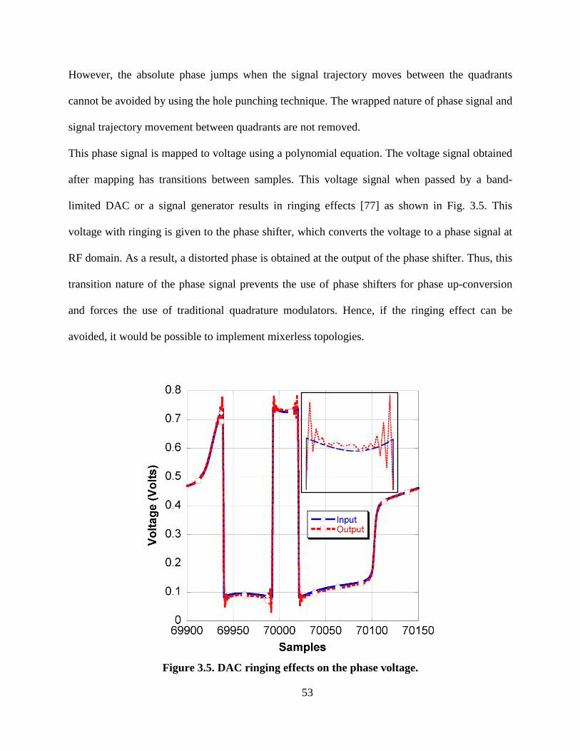
However, the absolute phase jumps when the signal trajectory moves between the quadrants
cannot be avoided by using the hole punching technique. The wrapped nature of phase signal and
signal trajectory movement between quadrants are not removed.
This phase signal is mapped to voltage using a polynomial equation. The voltage signal obtained
after mapping has transitions between samples. This voltage signal when passed by a band-
limited DAC or a signal generator results in ringing effects [77] as shown in Fig. 3.5. This
voltage with ringing is given to the phase shifter, which converts the voltage to a phase signal at
RF domain. As a result, a distorted phase is obtained at the output of the phase shifter. Thus, this
transition nature of the phase signal prevents the use of phase shifters for phase up-conversion
and forces the use of traditional quadrature modulators. Hence, if the ringing effect can be
avoided, it would be possible to implement mixerless topologies.
Figure 3.5. DAC ringing effects on the phase voltage.
53

3.5.1 Phase conditioning techniques
The issue of ringing and wrapped nature of the phase component were addressed in literature
using the following techniques.
Phase unwrapping
The phase signal extracted is wrapped between –pi and pi radians as mentioned above. This
phase signal was subjected to unwrapping to avoid these phase jumps [78, 79]. The phase
unwrapping removes the phase jumps and generates a continuous phase component signal.
However, the unwrapped phase signal had a huge range of values, which phase shifters won’t be
able to support.
Oversampling
The use of oversampling technique by interpolating the complex signal was expected to reduce
the ringing [80]. However, no significant change was observed in the ringing effect when large
oversampling ratio was applied to the complex signal.
Linear interpolation of phase component
DACs and signal generators use different pre-emphasis techniques to reduce the ringing effect in
square waves [81, 82]. A similar technique using linear interpolation of the phase was used to
reduce the ringing. However, this method could not be used as interpolation introduced phase
points, which caused huge distortion in the complex signal.
Filtering and Windowing techniques
Filtering and windowing techniques were used to shape the phase signal to avoid sharp
transitions and therefore reduce the ringing [83, 84]. However, these methods similar to the
interpolation techniques, introduced significant distortion to the complex signal.
54

Constellation shift
In this thesis, a different technique using constellation shift is proposed to nullify the effect of
ringing. The complex signal constellation is shifted, so that the signal trajectory is restricted
between the first and second quadrants as shown in Fig. 3.6. The phase component no longer has
transitions between –pi and pi radians as shown in Fig. 3.7 and is restricted between 0 and pi
radians. This constellation shift can be compensated in the receiver during demodulation. The
phase signal is extracted from the complex IQ after constellation shift. This phase signal is
mapped to voltage and this voltage is fed to the phase shifter. The LTE signal (^ ^I jQ+ ) after
applying constellation shift can be represented as
^ ^I jQ I j{Q (min(Q)}+ = + + (3.6)
where, I and Q are the inphase and quadrature components of the original LTE signal.
Figure 3.6. LTE complex signal trajectory after constellation shift.
55

Figure 3.7. Phase component of LTE signal after constellation shift.
3.6 Phase shifter imperfections
In practice, phase shifters do not have a linear phase response; the phase of the RF signal does
not vary linearly with the control voltage. This nonlinear dependence creates a phase-to-phase
(PM-PM) distortion in the complex signal.
Moreover, the amplitude of the signal at the output of the phase shifter, which should remain
constant as it propagates through the phase shifter, varies due to the device insertion loss
variation versus control voltage. Such variation creates a phase-to-amplitude (PM-AM) nonlinear
effect. Fig. 3.8 shows the phase and magnitude response of the phase shifter for a DC control
voltage. This PM-PM and PM-AM nonlinearity created by the phase shifter affects the quality of
the modulated signal produced at the output of the transmitter. Thus, the phase shifter too has to
be calibrated and modelled similarly to the VGA, to mitigate these imperfections.
56

In addition, the phase shifter exhibits phase noise errors, which limits the quality of the signal.
Figure 3.8. Phase shifter dc gain and phase response.
3.7 Phase shifter calibration
The phase response of the phase shifter and the memory effects can be modelled using a memory
polynomial and digital predistortion technique can be utilized to linearize the response. The
magnitude response of the phase shifter has to be corrected in an alternate chain where the
amplitude can be controlled. The following section describes the modelling and linearization of
the phase shifter nonlinearity using memory polynomial model.
57

3.7.1 Memory polynomial calibration
A memory polynomial model with positive real coefficients is used in this section in order to
model the nonlinear phase response of the phase shifter. The memory polynomial can be
represented as follows:
( ) ( )KM k 1
mkm 0 k 1
y n a x n m −
= == −∑∑ (3.7)
where, amk is the real valued predetermined calibration constant from a training signal. M is the
memory depth and K is the nonlinearity order of the memory polynomial. x(n) and y(n) represent
the input and output of the model, respectively. The memory polynomial models the nonlinear
phase and memory effects of the phase shifter in a single step. The input to the model is the
phase control voltage obtained from mapping and the output is the phase of the complex signal at
the output of the phase shifter. The generation of the real valued model coefficients and the
predistortion technique is done, similar to the method described in the case of VGA in chapter
two.
3.7.2 Digital predistortion of phase signal
The reverse model of the phase shifter is used to obtain the predistortion coefficients. For reverse
modelling, the phase of the complex signal at output of the phase shifter acts as input to the
model and the control voltage of the phase shifter acts as the output. Once the predistortion
coefficients are extracted, the original phase of the input signal is multiplied with these
coefficients and predistorted voltage is obtained. This predistorted voltage acts as the new
control signal of the phase shifter. This voltage is sent to the device and the output is observed.
Thus, predistortion model accounts for the linearization of the phase response of the phase
shifter, and also the mapping of the original phase signal to the phase control voltage.
58

3.8 Phase modulator implementation
The phase modulator architecture is implemented using the evaluation board (HMC928LP5E) as
depicted in Fig. 3.9. The phase information is extracted using (3.4) and mapped to voltage in
MATLAB.
ESG4438C
N5182A
MSO9404A
HMC928LP5E
THS3001CD
DSPDSP
Figure 3.9. Phase modulator using phase shifter implementation.
The phase control voltage is downloaded into the MXG/DAC (N5182A from Agilent
Technologies). The Local Oscillator (LO) signal is generated using a signal generator (E4438C
ESG from Agilent Technologies) and given to RF port of the phase shifter (HMC928LP5E). The
output of the DAC is given to an operational amplifier (THS 3001CD from Ti). The output of the
op-amp is connected to the phase control input of the phase shifter. The RF signal at output of
the phase shifter is captured using an oscilloscope (MSO9404 from Agilent Technologies) and
digitized using VSA software (89600 series VSA from Agilent Technologies). The time
alignment and further processing is carried out using MATLAB to retrieve the phase information
in the captured signal.
59

After alignment, the phases of the input signal (ϕin) and output signal (ϕout) are extracted and
multiplied with the original envelope signal (Ain) to obtain the input complex signal (Ainejϕin) and
output complex signal (Ainejϕout), respectively, and these two signals are compared using the
NMSE metric to evaluate the performance of the phase shifter. Hence, in this evaluation we have
assumed that the amplitude error of the phase shifter is zero and that the amplitude components
of the input and output complex signals are identical.
The NMSE is calculated as,
( ) ( ) ( )( )
2N
in out2
n 1 in
10S n S n1
N S nNMSE dB 10log
=
−
= ∑ (3.8)
where, Sin (Aejϕin) and Sout (Aejϕout) are the input and output complex signals, respectively.
3.9 Measurement results
To validate the calibration technique and to evaluate the performance of the phase shifter, a LTE
signal is generated in ADS software and sent into the setup as described above. The LTE signal
is oversampled by 16 and baseband signal has 100,000 samples, sampled at a rate of 30.72
Msamples/s. The LO signal is at 2.2 GHz and has a power level of -10 dBm. The measurement
results are summarized in Table 3.2.
Table 3.2 Summary of performance evaluation of phase shifter for LTE signal
SPECIFICATION VALUE
Signal bandwidth (MHz) 1.4
NMSE before constellation shift and linearization (dB) -22.41
NMSE after constellation shift and linearization (dB) -34.16
Nonlinearity order, Memory depth K = 4; M = 1
60

Figure 3.10. Phase signal (Φ) at input and output of the phase shifter.
The time domain representation of the phase at the output of the phase shifter after applying
constellation shift and linearization is shown in Fig. 3.10. The phase shifter accurately
reproduces the phase information at its RF output. In the absence of constellation shift, the phase
at the output of the phase shifter has distortion introduced from ringing and the measured NMSE
value is poor.
61

Figure 3.11. LTE signal spectrum at output of the phase shifter.
The modelling gives poor results and cannot compensate for the distortion. The NMSE value is
improved by more than 10 dB after adopting constellation shift and linearization. The spectrum
of the LTE signal at the output of the phase shifter is shown in Fig. 3.11. The amplitude
component of the input and output complex signals is identical. Hence, the only distortion in the
complex signal comes from the phase component. The signal distortion from ringing brings the
noise floor to a high value and limits the dynamic range of the signal.
62

Figure 3.12. Phase shifter input-output phase response.
Fig. 3.12 shows the input-output phase response of the phase shifter. This shows that the phase
response of the phase shifter is linearized after adopting predistortion technique using memory
polynomial model.
63

3.10 Conclusion
In this chapter, the implementation of a phase modulator using an analog phase shifter was
discussed. The working of phase shifter as a phase modulator was outlined. A new technique of
signal conditioning which involves constellation shift for OFDM signals was proposed to avoid
phase discontinuities.
The constellation shift avoids the ringing phenomenon that appears in the DACs, hence allowing
for the implementation of mixerless phase modulators. The limitation of the phase shifter in
terms of its nonlinear phase response was discussed. Consequently, the calibration technique
utilized to mitigate these limitations was discussed. A memory polynomial was used to model
the nonlinear phase response of the phase shifter. The performance of the phase shifter using the
proposed technique for a LTE signal of 1.4 MHz bandwidth improved the signal quality in terms
of NMSE from -22 dB before constellation shift to -34 dB after constellation shift and
linearization.
64

Mixerless Polar Modulator-Based Transmitter Architecture Chapter Four:
4.1 Introduction
The performance of the VGA as an amplitude modulator and the phase shifter as a phase
modulator was evaluated in chapter two and chapter three, respectively. In this chapter, a new
transmitter architecture based on a mixerless polar modulator topology, which uses a VGA for
amplitude modulation and a phase shifter for phase modulation, is proposed. This architecture is
realised without using a mixer or quadrature up-converter as compared to RFDAC-based
transmitters mentioned in literature. The VGA and the phase shifter have imperfections, which
affect the quality of the RF signal at the output of the transmitter. A new calibration technique is
proposed in this work to mitigate these imperfections simultaneously. The implementation of the
new architecture is discussed and the performance is evaluated using an LTE signal.
4.2 Mixerless polar modulator-based transmitter
DSP
VGA
Phase Shifter
LO
RF O/P
Phase voltage
Envelope voltage
I
Q
Figure 4.1. Block diagram of the mixerless polar modulator-based transmitter architecture.
65

The block schematic of the proposed transmitter architecture is shown in Fig. 4.1. The IQ signal
is decomposed into amplitude and phase components. The amplitude and phase components are
mapped to gain and phase control voltages, which drive the VGA and the phase shifter,
respectively. A RF continuous wave (CW) signal is given to the RF input of the phase shifter.
The output of the phase shifter has a phase modulated RF signal with a constant envelope. This
RF output signal is fed into the RF input of the VGA. The VGA inserts the amplitude
information to this phase-modulated RF signal to generate a complex RF signal at the output of
the VGA. Mixer circuits or quadrature modulators are not used for translating the baseband
phase or amplitude signal to RF domain. This nullifies the spurious emissions and distortion
associated with the mixers. Consequently, the need for filtering the mixer spurs is avoided.
4.3 VGA gain and phase response
Figure 4.2. VGA AM-AM response.
66

The VGA has a nonlinear amplitude and phase response as described in chapter 2. The amplitude
driven amplitude (AM-AM) response and the amplitude driven phase (AM-PM) response of the
VGA are shown in Fig. 4.2 and Fig. 4.3. The amplitude nonlinearity and the memory effects of
the VGA were mitigated using memory polynomial modelling technique in chapter 2. However,
the phase response of the VGA cannot be corrected in the same path and has to be compensated
in another path, where the phase of the signal can be controlled.
Figure 4.3. VGA AM-PM response.
67
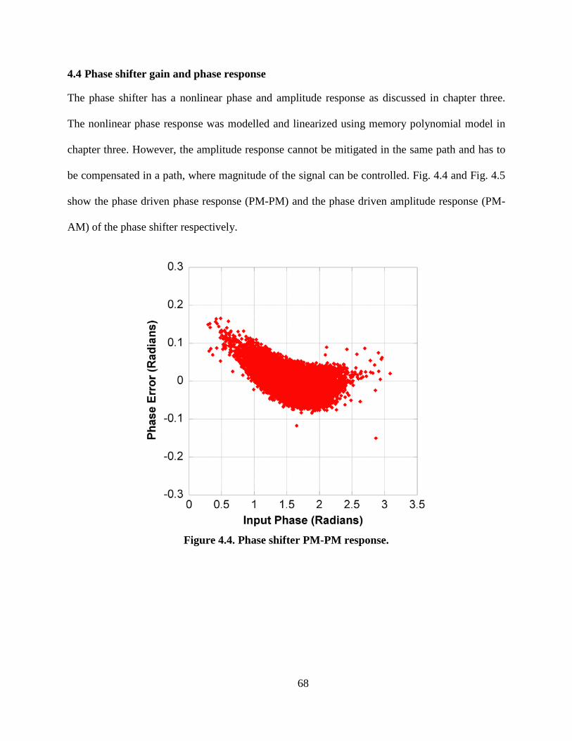
4.4 Phase shifter gain and phase response
The phase shifter has a nonlinear phase and amplitude response as discussed in chapter three.
The nonlinear phase response was modelled and linearized using memory polynomial model in
chapter three. However, the amplitude response cannot be mitigated in the same path and has to
be compensated in a path, where magnitude of the signal can be controlled. Fig. 4.4 and Fig. 4.5
show the phase driven phase response (PM-PM) and the phase driven amplitude response (PM-
AM) of the phase shifter respectively.
Figure 4.4. Phase shifter PM-PM response.
68

Figure 4.5. Phase shifter PM-AM response.
4.5 Calibration of the proposed transmitter architecture
The proposed transmitter architecture using the VGA and the phase shifter will exhibit all the
four responses mentioned above: AM-AM, AM-PM, PM-PM and PM-AM. This will deteriorate
the quality of the RF signal produced at the output of the transmitter and will introduce
significant amount of distortion. A possible technique is to use individual predistortion models
for the VGA and the phase shifter to linearize their responses. Also, the phase response of the
VGA should be corrected in the phase shifter and magnitude response of the phase shifter should
be compensated in the VGA. However, this technique cannot be implemented as the responses
are interdependent. Hence, use of individual predistortion models for the amplitude and phase
paths is not an optimum solution. A new calibration technique is proposed in this work to model
the architecture as a single block.
69

This calibration technique considers the transmitter as one block and the original input complex
signal and the complex signal at the output of transmitter are used for modelling.
4.5.1 Modified memory polynomial calibration
A modified memory polynomial is proposed to model the mixerless polar-modulator-based
transmitter architecture. The proposed model can be represented as
( ) ( ) ( )M K k
m 0 k 0 j 0
k jjy n a x n m x n mmkj= = =
−= − × −∑∑∑ (4.1)
where, amkj is the complex predetermined model coefficient from a training signal. M is the
memory depth and K is the nonlinearity order of the modified memory polynomial for the nth
sample. x(n) and y(n) represent the input and output complex signals respectively. Since this
modified memory polynomial model includes terms having the complex envelope to the power
of j, this model is capable of modeling PM-PM and PM-AM effects to certain extent. The
complex gain (transfer function) of the proposed modified memory polynomial is a function of
the amplitude as well as phase of the input signal. Therefore, this proposed model is expected to
be able to improve the linearity performance compared to a conventional memory polynomial,
whose transfer function is dependent only on the amplitude of the input and hence, is able to
compensate only for the AM-AM and AM-PM nonlinear effects. A training sequence of 20,000
samples is used to extract the model coefficients. The coefficients are extracted using Least
Squares technique as described in chapter two. Using the extracted coefficients and the original
input signal, the output complex signal is estimated. This estimated output signal is compared
with the measured output signal of the transmitter using the NMSE metric to evaluate the
performance of the model. The following section briefly describes the steps involved in this
calibration technique.
70

Consider ( ) ( ) ( )j k jk n mB x n m x n m −− = − × −∣ ∣ (4.2)
The calibration matrix, B generated for the above proposed model can be represented as,
( ) ( ) ( ) ( )( ) ( ) ( ) ( )
( ) ( ) ( ) ( )
K 1 K
1 K 1 K
1
1 K 1 K
B n B n B n M ..B n M
B n 1 ..B n 1 B n 1 M ..B n 1 M
B n p 1 ..B n p 1 B n p 1 M ..B n p 1 M
B
− −
+ + + − + −
+ − + − + − − + − −
=
..
(4.3)
Here x(n) refers to the input and y(n) refers to the output samples and p is the number of samples
of the signal portion used for the model identification.
The output matrix Y can be represented as,
( )( )
( )
y ny n 1
Y .
y n p l
+ = …
+ −
(4.4)
The coefficient vector a can be represented as,
a a a a a000 010 jK0 001 jKMT
a ... = (4.5)
Using the Least Squares technique, following equation holds,
Ba Y= (4.6)
The coefficient vector a is obtained as,
†a B Y= (4.7)
where, †B is the pseudo-inverse of B.
This is obtained in MATLAB using the pseudo-inverse function (pinv).
( )a pinv B Y= × (4.8)
The coefficients thus obtained, is multiplied with the complete input signal to get an estimate of
the output, Yest
71

est
Y Ba= (4.9)
Yest is compared with the actual output Y to evaluate the model performance.
4.5.2 Digital predistortion technique
The complete transmitter architecture is modelled as a single block as described above. For
forward modelling, the input IQ signal acts as the input to the model and the captured output of
the transmitter acts as the output.
Using similar technique and swapping the input and output signals, the reverse model of the
transmitter is obtained. The reverse model coefficients are multiplied with the original complex
IQ signal to generate the predistorted IQ signal. The predistorted IQ signal is subjected to
decomposition into amplitude and phase components and further processing, to generate the new
control voltages. The complete transmitter architecture along with the signal processing block is
shown in Fig. 4.6.
Signal
VGAMapping
VGA phase
compensation
Delay
Phase shifter
Operational amplifier
Local oscillator
RF output
Digital Analog
Envelope
Phase
Predistortion &
decomposition
Mapping
Figure 4.6. Block schematic of the proposed mixerless polar-modulator-based transmitter.
72
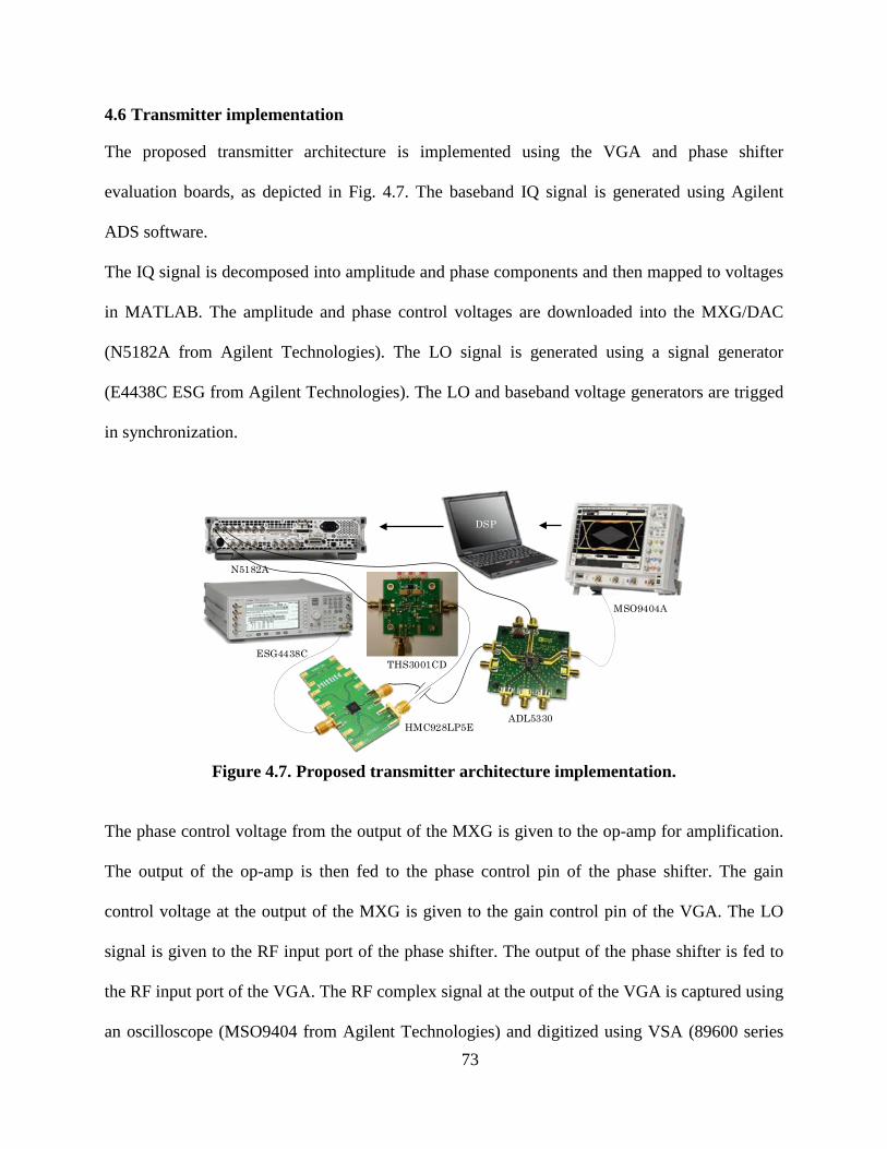
4.6 Transmitter implementation
The proposed transmitter architecture is implemented using the VGA and phase shifter
evaluation boards, as depicted in Fig. 4.7. The baseband IQ signal is generated using Agilent
ADS software.
The IQ signal is decomposed into amplitude and phase components and then mapped to voltages
in MATLAB. The amplitude and phase control voltages are downloaded into the MXG/DAC
(N5182A from Agilent Technologies). The LO signal is generated using a signal generator
(E4438C ESG from Agilent Technologies). The LO and baseband voltage generators are trigged
in synchronization.
DSP
ESG4438C
N5182A
MSO9404A
ADL5330HMC928LP5E
THS3001CD
DSPDSP
Figure 4.7. Proposed transmitter architecture implementation.
The phase control voltage from the output of the MXG is given to the op-amp for amplification.
The output of the op-amp is then fed to the phase control pin of the phase shifter. The gain
control voltage at the output of the MXG is given to the gain control pin of the VGA. The LO
signal is given to the RF input port of the phase shifter. The output of the phase shifter is fed to
the RF input port of the VGA. The RF complex signal at the output of the VGA is captured using
an oscilloscope (MSO9404 from Agilent Technologies) and digitized using VSA (89600 series 73

VSA from Agilent Technologies). The time alignment and further processing is carried out using
MATLAB to retrieve the IQ information in the captured signal.
4.7 Measurement results
The performance of the proposed transmitter architecture is validated using the same LTE signal
used for the performance evaluation of the VGA and the phase shifter. A LTE signal of 1.4 MHz
bandwidth is generated using Agilent ADS software and sent to the set-up as described above.
The performance is measured over a sample length of 200,000 samples at a sampling rate of
30.72 Msamples/s. The Local Oscillator (LO) signal is at a frequency of 2.2 GHz and has a
power level of -10 dBm. The captured IQ signal after time alignment is loaded into the VSA
software. The VSA software demodulates the IQ signal, removes the OFDM carriers and gives
back the signal constellation. The constellation thus obtained, is compared with the standard LTE
constellation defined in VSA and the EVM is calculated. The summary of results of the
performance evaluation of the proposed architecture for LTE signal with QPSK constellation is
given in Table 4.1 and Table 4.2.
Table 4.1 Summary of performance evaluation of proposed transmitter for LTE signal
SPECIFICATION VALUE
Signal bandwidth (MHz) 1.4
EVM before digital predistortion (%) 10.48
EVM after using normal memory polynomial model (%) 1.47
EVM after using proposed modified memory polynomial model (%) 0.59
Nonlinearity order and Memory depth K = 4; M = 1
74

Table 4.2 Measured ACLR values of the proposed transmitter for LTE signal
SPECIFICATION VALUE
ACLR before digital predistortion (dBc) 43.16
ACLR after using normal memory polynomial model (dBc) 49.08
ACLR after using proposed model (dBc) 56.72
Table 4.3 Transmit EVM* specifications for wide area BS [85]
MODULATION SCHEME
REQUIRED EVM [%]
QPSK 17.5
16 QAM 12.5
64 QAM 8 NOTE*: The minimum EVM requirements listed in [77] represent the combined EVM of the entire transmitter chain that includes the base band modulator, the digital-to-analog converter (DAC), the RF transmitter and the RF power amplifier.
Table 4.4 ACLR requirements of E-UTRA (LTE) [85]
E-UTRA TRANSMITTED SIGNAL CHANNEL BANDWIDTH BWCHANNEL [MHZ]
BS ADJACENT CHANNEL CENTRE FREQUENCY OFFSET BELOW THE FIRST OR ABOVE THE LAST CARRIER CENTRE FREQUENCY TRANSMITTED
ASSUMED ADJACENT CHANNEL CARRIER
FILTER ON THE ADJACENT CHANNEL FREQUENCY AND CORRESPONDING FILTER BW
ACLR LIMIT
1.4, 3.0, 5, 10, 15, 20
BWChannel E-UTRA of same BW Square (BWConfig) 45 dB
2 x BWChannel E-UTRA of same BW Square (BWConfig) 45 dB
BWChannel /2 + 2.5 MHz 3.84 Mcps UTRA RRC (3.84 Mcps) 45 dB
BWChannel /2 + 7.5 MHz 3.84 Mcps UTRA RRC (3.84 Mcps) 45 dB
NOTE 1: BWChannel and BWConfig are the channel bandwidth and transmission bandwidth configuration of the EUTRA transmitted signal on the assigned channel frequency. NOTE 2: The RRC filter shall be equivalent to the transmit pulse shape filter defined in TS 25.104, with a chip rate as defined in this table.
75

The EVM has improved by more than 10 % after adopting digital predistortion using the
proposed model. The linearization technique reduces the signal distortion to a great extent. The
new model gives better performance as compared to the normal memory polynomial model. The
EVM value obtained also meets the EVM requirements of the LTE standard as shown in Table
4.3. The improvement in EVM validates the performance of the proposed black-box modelling
technique. The ACLR has also improved by 13 dB and the value obtained conforms to the 3GPP
LTE standard requirements, summarized in Table 4.4. The spectrum of the signal at the output of
the transmitter is shown in Fig. 4.8. This shows the mitigation of the signal distortion by
adopting predistortion using the proposed calibration technique.
Figure 4.8. LTE signal spectrum at the output of the polar transmitter.
76

The performance of the proposed transmitter for LTE signal of 1.4 MHz bandwidth, with 64
QAM signal constellation is summarized in Table 4.5.
Table 4.5 EVM measurements for LTE signal with 64 QAM constellations
SPECIFICATION VALUE
EVM before digital predistortion (%) 9.97
EVM after using proposed modified memory polynomial model (%) 1.72
The AM-AM and AM-PM responses of the proposed transmitter architecture are shown in Fig.
4.9 and Fig. 4.10, respectively. The gain and phase responses of the transmitter are linearized to
a great extent using the proposed model. Thus, the new model is able to linearize the nonlinear
amplitude and phase response of the devices in a single step.
Figure 4.9. Transmitter AM-AM response.
77

Figure 4.10. Transmitter AM-PM response.
The performance of the proposed transmitter is also evaluated for higher bandwidth LTE signals
with 64 QAM constellations and is summarized in Table 4.6.
Table 4.6 Performance evaluation using LTE signals of 5 and 10 MHz bandwidth
SPECIFICATION 5 MHZ 10 MHZ
EVM before digital predistortion (%) 10.77 12.70
EVM after using proposed model (%) 1.38 2.92
ACLR before DPD (dBc) 36.58 33.68
ACLR after DPD (dBc) 48.75 44.12
Fig. 4.11 and Fig. 4.12 show the spectral response of the proposed transmitter for LTE signals of
5 MHz and 10 MHz bandwidth, respectively.
78

Figure 4.11. Spectrum of LTE signal of 5 MHz bandwidth.
Figure 4.12. Spectrum of LTE signal of 10 MHz bandwidth.
79

The wideband spectral response of the proposed transmitter architecture is shown in Fig. 4.13.
This response is compared with that of a commercially available IQ modulator from Signal Core.
The LO frequency used was 2.2 GHz. The proposed topology does not have any spurious
emissions over a wide frequency range. The second harmonic of the LO (4.4 GHz) has a very
low power as compared to the IQ modulator. Thus, the proposed architecture does not require
any filtering at the output. This also negates the use of band-specific filters at the output of the
proposed transmitter architecture.
Figure 4.13. Wide band spectral response of the proposed transmitter.
80

4.8 Constellation shift compensation
As described in chapter three, the LTE baseband signal is subjected to a constellation shift to
avoid the phase discontinuities. The LTE baseband signal after applying constellation shift is
represented as,
^ ^I jQ I j{Q (min(Q)}+ = + + (4.10)
where, I and Q are the inphase and quadrature components of the original LTE signal.
The addition of a dc value to the quadrature component (Q), results in the multiplication of the
carrier or CW signals with the DC term during frequency up-conversion. Thus, the up-converted
signal has the RF carrier component, centered around the particular LO frequency. This RF
signal after the modulator passes through the RF PA and gets amplified. Thus, the PA amplifies
the signal as well as the unwanted RF carrier signal. The power of the signal after addition of DC
component using (4.10) increases by almost 9 dB. This is due to the DC component which gets
translated to RF as the carrier. Thus the generated signal contains a non-useful carrier signal in
addition to the useful information. This carrier signal gets amplified by the PA, which will
consume additional unwanted DC power. This unwanted DC power affects the efficiency of the
PA. To avoid this unwanted carrier from being amplified, the addition of DC component through
constellation shift has to be compensated before the PA. The constellation shift can be
compensated by using a multi-branch architecture for the proposed polar modulator-based
transmitter as shown in in Fig. 4.14.
81

DSP
VGA
Phase Shifter
LORF O/P
Phase voltage
Envelope voltage
Envelope voltage
DSP
Phase Shifter
VGA
Phase voltage
I+jQ-dc
180
I+jQ+dc
Figure 4.14. Multi-branch polar modulator-based transmitter for dc compensation.
A constellation shift is applied to the LTE signal and can be represented as,
^ ^I jQ I j{Q (min(Q)}+ = + + (4.11)
" "I jQ I j{Q (min(Q)}+ = + − (4.12)
where, I and Q are the inphase and quadrature components of the original LTE signal.
The first complex signal (^ ^I jQ+ ) is sent through the first branch of the modulator. The second
complex signal (" "I jQ+ ) is sent through the lower branch. The RF complex LTE signals at the
output of the two branches are summed together before the PA.
The carrier components cancel out, as they are 180 degrees out-of-phase. The performance of the
proposed multi-branch topology was tested for LTE signals of 1.4 MHz and 5 MHz bandwidths
and the measurement results are summarized in Table 4.7.
82

Table 4.7 Summary of performance evaluation of multi-branch topology
SPECIFICATION 1.4 MHZ 5 MHZ
EVM before digital predistortion (%) 9.82 10.49
EVM after digital predistortion (%) 0.43 0.59
ACLR before DPD (dBc) 50.15 42.83
ACLR after DPD (dBc) 59.05 51.43
The results show that the multi-branch topology has better performance in terms of EVM as
compared to the single branch topology. The ACLR values have improved by 3 dB as compared
to that of the single branch architecture mentioned in Table 4.1 and Table 4.6.
Figure 4.15. LTE signal spectrum at the output of multi-branch topology.
83

Fig. 4.15 and Fig. 4.16 show the spectral responses of the LTE signals of 1.4 MHz and 5 MHz
bandwidths at the output of the multi-branch polar modulator-based transmitter architecture,
respectively.
Figure 4.16. Spectrum of LTE signal with 5 MHZ bandwidth.
84

4.9 Conclusion
In this chapter, a new transmitter architecture using a RF VGA and a phase shifter to build a
mixerless polar modulator was proposed. The amplitude and phase responses of the devices were
evaluated. The nonlinear gain and phase responses of the devices introduced significant
distortion to the signal at the output of the proposed transmitter. A new calibration technique was
proposed to mitigate the imperfections in the VGA and the phase shifter. A modified memory
polynomial was proposed to model the transmitter as a single black-box model. The
implementation of the proposed architecture using evaluation boards for the VGA and the phase
shifter was discussed. The proposed architecture and the proposed calibration technique were
tested using a LTE signal. The performance of the transmitter was measured and evaluated using
EVM metric. The EVM of the LTE signal was improved from 10% to 0.4% and the ACLR was
improved to 59 dBc using the proposed digital predistortion model. The proposed calibration
technique mitigated the nonlinear amplitude and phase responses of both the VGA and the phase
shifter together. The constellation shift applied to avoid phase discontinuities is compensated by
using a multi-branch topology for the proposed architecture. The multi-branch architecture offers
better signal quality in terms of EVM and ACLR and avoids any requirement for DC
compensation circuits at the receiver.
The new transmitter architecture translates the baseband IQ signal to RF without using a mixer
or a quadrature up-converter. The transmitter does not have any spurious emissions over a wide
frequency band as compared to that of a conventional IQ modulator. Thus, the proposed
architecture does not require any filtering at the output. Hence, the use of band-specific filters at
the output of transmitter is not required as compared to transmitter architectures based on
RFDACs in literature.
85

Three-way Amplitude Modulation-Based Transmitter Architecture Chapter Five:
5.1 Introduction
The performance of the proposed mixerless polar transmitter architecture was evaluated in
chapter four. The complete transmitter architecture was modelled using modified memory
polynomial. The transmitter topology exhibited good performance for LTE signals of different
bandwidths. The RF signal at the output of the VGA has a good dynamic range and the VGA has
very low emissions at its output. The phase shifter reproduces the baseband phase information at
its RF output. The phase shifter has issues with noise and affects the quality of RF signal
produced at its output. The phase shifter when driven with a constant control voltage exhibited
phase variations at the output over a period of time. These phase variations could not be
modelled and compensated for by the proposed impairment compensation technique. This
behaviour is uncorrelated with the signal, which makes them appear as phase noise at the output
of the transmitter. This distortion introduced by the phase shifter affects the overall quality of the
RF signal at the output of the proposed transmitter architecture.
A constellation shifting technique, as described in chapter three is used to avoid the phase
discontinuity and ringing effects from the DAC. The addition of DC in this constellation shift is
compensated through a multi-branch architecture for the polar modulator-based transmitter as
shown in chapter four.
The implementation and performance evaluation of this architecture using the VGA and the
phase shifter gave a way to another transmitter architecture. The idea was to implement a method
to take the baseband IQ signal to RF domain without using mixers, frequency up-converters and
phase modulator circuits such as a phase shifter or a PLL.
86

A new transmitter topology, called the three-way amplitude modulation-based transmitter, which
uses only envelope modulators, is proposed in this chapter. The concept of this architecture is
based on decomposing the complex envelope of the signal into three envelope components using
a three-coordinate decomposition algorithm. Three variable gain amplifiers act as envelope
modulators for these three components in order to translate the baseband signal to a carrier
frequency. This architecture does not have any phase modulator circuit and avoids any issues
with the transitional nature of the phase component.
5.2 Three-coordinate decomposition
The original complex IQ signal can be represented in polar format as (r, θ) where, r is the
magnitude and θ is the angle.
2 2r I Q= + (5.1)
1 Qθ tanI
− =
(5.2)
where, I and Q are the inphase and quadrature components.
X
Y
Z
xcomponent
ycomponentθ
r
I+jQ
Figure 5.1. Three-coordinate signal decomposition.
87

Based on geometric equations described below, a point I+jQ of magnitude r and angle θ can be
decomposed into three positive real components; x, y and z, which are 120 degrees apart as
shown in Fig. 5.1.
θ a
c b
A
B
C
Figure 5.2. Law of sines representation.
Consider ΔABC with a, b and c as the length of the sides and ϕ, θ, Ψ as the angles as shown in
Fig. 5.2. According to the law of sines [86], we have a relation,
b c a sin θ sin sin Ψ
= =φ
(5.3)
The value of a can be obtained as,
csin Ψasin
=φ
(5.4)
Using the above relation, x, y and z components in Fig. 5.1 can be obtained as
( )r sin 120 θx
sin60−
= (5.5)
rsinθysin60
= (5.6)
Similarly, the value of the z component can be calculated when the angle θ is greater than 120
degrees.
88

Thus, any complex point with a magnitude r and an angle θ can be decomposed into x, y and z
components. The x, y and z components, when out-phased by 0, 120 and 240 degrees, three
vectors are obtained which when added result in a vector that represents the complex envelope of
the signal. The three-coordinate decomposition ensures that the components x, y and z are non-
negative.
The x, y and z components are mapped to voltages as,
( )10vctrl 20×alog component b= + (5.7) where, a and b are the constants obtained from DC voltage gain response of the VGA. Thus,
using the above relation the gain control voltages vx, vy and vz are obtained.
5.3 Three-way amplitude modulation-based transmitter architecture
120˚
240˚
0˚
Local oscillator
DSP
VxVyVz
I
Q
RF output
VGAx
VGAy
VGAz
Figure 5.3. Three-way amplitude modulation-based transmitter architecture.
89

The proposed transmitter architecture is shown in Fig. 5.3. It consists of three envelope
modulators, VGAx, VGAy and VGAz whose gains are controlled by the voltages vx, vy and vz,
respectively. The working of VGA as an envelope modulator has been described in chapter two.
A Local Oscillator signal (LO) is given to a three-way power divider. Each of these LOs at the
output of the power divider is given a phase shift of 0, 120 and 240 degrees using passive
components and then given to RF input port of VGAx, VGAy and VGAz, respectively.
The gain control voltages act as modulating signals and amplitude modulated signals are
obtained at the RF output of the VGAs. Thus, at the output of the three VGAs we have the x, y
and z components translated to RF and with the required phase shifts. The RF outputs of the
three VGAs are summed together using a three-way power combiner to obtain the complex RF
signal. The power combiner/divider and the phase rotation components can be designed using
microstrip transmission lines. These are passive components and can be designed for broadband
applications. The VGAs operate over a wide RF bandwidth and do not have any spurious
emissions and hence, the transmitter is devoid of any filtering requirements. Thus, this proposed
architecture facilitates the translation of baseband IQ signal to RF without using mixers, up-
converters and phase modulator circuits.
5.4 VGA phase response
The VGA has a phase response as discussed in chapter two. The phase of the LO signal varies as
it propagates through the VGA. The variation of phase at the output of the VGA as a function of
gain control voltage is shown in Fig. 5.4.
90
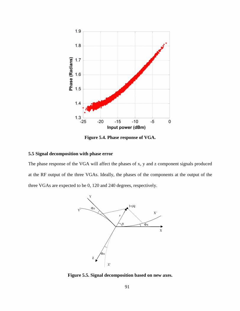
Figure 5.4. Phase response of VGA.
5.5 Signal decomposition with phase error
The phase response of the VGA will affect the phases of x, y and z component signals produced
at the RF output of the three VGAs. Ideally, the phases of the components at the output of the
three VGAs are expected to be 0, 120 and 240 degrees, respectively.
X
Y
Z
θ
r
I+jQ
X^Y^
Z^
Фx
Фz
Фy
Figure 5.5. Signal decomposition based on new axes.
91

However, from Fig. 5.4, we see that the phase of the RF signal at the output of the VGA varies
with the gain control voltage. For a given sample n, the phase of the components x, y and z at the
output of VGAs; VGAx, VGAy and VGAz can be represented as 0°+Φx(n), 120°+Φy(n) and
240°+Φz(n), respectively. Here Φx(n), Φy(n) and Φz(n) are the phase errors in degrees introduced
by the VGAs; VGAx, VGAy and VGAz, respectively for the nth sample.
To compensate this phase error, the complex point I+jQ is decomposed into components along,
0°+Φx(n), 120°+Φy(n) and 240°+Φz(n) axes as shown in Fig. 5.5. The new axes are represented as
X^, Y^ and Z^. Based on the new axes and using the law of sines, the complex point I+jQ of
magnitude r and angle θ can be decomposed into new components; x^, y^ and z^ as
^r sin 120 y
xsin 60 x y
− θ+ φ = + φ −φ
(5.8)
( )^
r sin xysin 60 x y
θ−φ=
+ φ −φ
(5.9)
Similarly, the z^ component is obtained when θ is greater than 120°+Φy(n) degrees. These new
components are mapped to voltages using (5.7) and the new voltages vx, vy and vz are obtained.
5.6 VGA calibration
The nonlinear gain response and the memory effects exhibited by the VGA can be modelled
using memory polynomial as described in chapter two. In this chapter, the calibration matrix is
modified to model the phase response of the VGA as well. The following section describes the
modelling and linearization of the gain and phase response of the VGA using memory
polynomial.
92

5.6.1 Memory polynomial calibration
A conventional memory polynomial model can be represented as,
( ) ( ) ( )M N
k 1mk
m 0 k 1y n a x n m x n m −
= == − × −∑∑ ∣ ∣ (5.10)
where, amk is the complex model coefficient that can be predetermined from a training signal. M
is the memory depth and K is the nonlinearity order of the memory polynomial model. x(n) and
y(n) represent the input and the output signals of the VGA, respectively. The memory
polynomial models the static nonlinearity and nonlinear memory effects of the VGA in a single
step. A training sequence of 10,000 samples is used to extract the model coefficients. The
coefficients are extracted using the Least Squares technique as described in chapter two. Using
the extracted coefficients and the original input signal, the output complex signal is estimated.
This estimated output signal is compared with the measured output signal of VGA using the
NMSE metric to evaluate the performance of the model. The following section briefly describes
the steps involved in calibration technique, adopted for modelling the gain as well as the phase
response of the VGA.
Consider ( ) ( ) ( ) k 1k n mB x n m x n m −− = − × −∣ ∣ (5.11)
The memory polynomial mentioned in (5.10) can be written in matrix format as,
( ) ( ) ( ) ( )( ) ( ) ( ) ( )
( ) ( ) ( ) ( )
( )
( )
K 1 K
1 K 1 K
K 1 K
1
1
10
20
K0
1M
KM
B n B n B n M ..B n M y n
B n 1 ..B n 1 B n 1 M ..B n 1 M y(n 1)
y n p 1B n p 1 ..B n p 1 B n p 1 M ..B n p 1 M
aaaa
a
− −
+ + + − + − +
+ −+ − + − + − − − −
=
+
..
(5.12)
93

Here x(n) refers to the input and y(n) refers to the output samples and p is the number of samples
of the signal portion used for the model identification.
The output matrix Y can be represented as,
( )( )
( )
y ny n 1
Y .
y n p l
+ = …
+ −
(5.13)
The coefficient vector a can be represented as,
a a a a aKM00 10 K0 0T
..1a .= (5.14)
Here, the calibration matrix is modified as compared to the method described in chapter two, to
add DC terms in the matrix. The modified matrix can be written as,
( ) ( ) ( ) ( )( ) ( ) ( ) ( )
( ) ( ) ( ) ( )
( )
( )
K 1 K
1 K 1 K
K 1 K
1
1
10
20
K0
1M
KM
1 B n B n B n M ..B n M y n
1 B n 1 ..B n 1 B n 1 M ..B n 1 M y(n 1)
y n p 11 B n p 1 ..B n p 1 B n p 1 M ..B n p 1 M
1
aaaa
a
− −
=+ + + − + − +
+ −+ − + − + − − + − −
..
(5.15)
Using the Least Squares technique, the coefficient vector, a is obtained as
†a B Y= (5.16)
where, B† is the pseudo-inverse of B.
The coefficients thus obtained, is multiplied with the complete input signal to get an estimate of
the output, Yest
est
Y B a= ⋅ (5.17)
Yest is compared with the actual output Y to evaluate the model performance.
94

5.6.2 Digital predistortion technique
The x component signal generated using (5.8) is mapped to a control voltage, vx using (5.7).
This voltage when sent to the VGAx, a complex signal is obtained at the output. For forward
modelling, the x component acts as the input and the measured complex signal acts as the output
of the model. The input and output signals are swapped to obtain the reverse model of the VGA.
Thus, for the reverse model, the input is complex and has both the magnitude and phase
information, while the output is real and has only the magnitude component.
Forward model
VGA
xInput
x
Reverse model
xestx′ ejΦx
x′ ejΦxOutput
Predistorterx″ xejΦx
VGA
Output
x′ ejΦxest
Figure 5.6. Predistortion and linearization.
To generate a complex input for the predistorter, xcomponent signal is multiplied with the
measured phase error from VGAx. This generated complex signal, is multiplied with the reverse
model coefficients as shown in Fig. 5.6. At the output of the predistorter, we obtain a quasi-real
predistorted x component signal with negligible phase information (the phase is very close to
zero and can be neglected to obtain a real signal without having a significant effect on the signal
95

quality). The residual phase of the predistorted signal is approximated to zero as the modulating
signal can have only real values. The predistorted signal is mapped to voltage and sent to the
VGA.
5.7 DSP block
The signal processing block as mentioned in Fig. 5.3 can be represented along with the
predistorter as shown below.
Decomposition 0˚,120˚,240˚
I
QPhase
mapping Φx,Φy,Φz
VGAx DPD
VGAy DPD
VGAz DPD
DACx
vz
vy
vx
Update Φx, Φy, Φz
xejΦx
yejΦy
zejΦz
x′′
y′′
z′′
Voltagemapping DACy
DACz
DSPDPD model coefficients
Decomposition 0˚+Φx
120˚+Φy 240˚+Φz
Filtering and compensation
Figure 5.7. Block schematic of the DSP.
The complex IQ signal is decomposed into x, y and z components along 0°, 120° and 240° axes
using (5.5) and (5.6). The components generated are mapped to corresponding phase errors, Φx,
Φy and Φz using the DC phase response of the VGA. The complex signal is subjected to a new
decomposition along, 0°+Φx(n), 120°+Φy(n) and 240°+Φz(n) axes using (5.8) and (5.9).
An offset value is added to the components to ensure non zero values. Then, the components are
subjected to digital filtering to avoid the discontinuities.
96

Figure 5.8. Components obtained after signal decomposition.
Figure 5.9. Xcomponent after filtering and compensation.
97

The variation in the component values after filtering and offset addition is also compensated. Fig.
5.8 shows the time domain plots of the x, y and z components obtained from complex signal
decomposition along new axes. The xcomponent after filtering and offset compensation is shown
is Fig. 5.9. The x, y and z components are then multiplied with the corresponding phase errors to
generate complex inputs. These complex signals are multiplied with their respective DPD
coefficients. The phase errors Φx, Φy and Φz and the DPD coefficients are updated after each
iteration.
Baseband signal
Decomposition along 0, 120, 240 axes
Decomposition along 0+Φx, 120+Φy, 240+Φz axes
Filtering and compensation
Φx, Φy, Φz
Generate complex signals for DPD
Predistorter and voltage mapping
Capture baseband signal
Signal generator
VGAs
x, y, z
x^, y^, z^
x~, y~, z~
x~ejΦx, y~ejΦy, z~ejΦz
vx, vy, vz
Gain control voltage
Analysis & iteration
Figure 5.10. Flow chart of DSP operation.
98

The output of the DPD models are approximated to real values and then subjected to voltage
mapping to obtain the control voltages vx, vy and vz, which are downloaded to the signal
generator. The different DSP operations can be summarized in a flow chart as given in Fig. 5.10.
5.8 Implementation of transmitter architecture
The implementation of the complete transmitter architecture involves the design and
implementation of three-way power divider and combiner and the phase rotation elements. To
generate the three analog control voltages, a three-output signal generator is required or multiple
generators have to operate in synchronization.
ESG4438C
N5182A
MSO9404AADL5330
DSP
Figure 5.11. Implementation of single path of transmitter.
For the proof of concept, in this thesis work the three VGAs are operated separately. The three
control voltages are generated and fed to the VGAs one after the other. The RF output of each
VGA is captured separately using a spectrum analyser and digitized using VSA software. The
power combining and the phase rotation operations are performed in digital domain after
obtaining the baseband signal from the VSA software.
99

Fig. 5.11 shows the implementation of the envelope modulator. The VGA evaluation board
(ADL5330), used in the previous architecture is used here. The control voltage, vx is sent into
the MXG/DAC (N5182A from Agilent Technologies). The Local Oscillator (LO) signal is
generated using a signal generator (E4438C ESG from Agilent Technologies). The LO signal
and baseband voltage generators are triggered in synchronization. The baseband output of the
MXG provides the analog control voltage, which is introduced to the gain control pin of VGAx.
The LO signal is fed to RF input port of VGAx.
The RF signal at the output of VGAx is captured using spectrum analyser (E4440 PSA from
Agilent Technologies) and digitized using VSA software (89600 series from Agilent
Technologies). The baseband outputs of the three VGAs are captured individually. The time
alignment and further processing is carried out using MATLAB. The output of VGAy and VGAz
are subjected to a phase rotation of 120 and 240 degrees, respectively. After the phase rotation
operation, the outputs of VGAx, VGAy and VGAz are summed together to obtain the complex
output signal. This signal is compared with the actual input complex signal and the NMSE value
is calculated.
5.9 Measurement results
To validate the proposed calibration technique and to evaluate the performance of the proposed
transmitter architecture, a LTE signal with QPSK constellation is generated using ADS software.
The LTE signal is oversampled by 16 and the baseband signal has 100,000 samples, sampled at a
rate of 30.72 Msamples/s. The complex signal is subjected to decomposition and processing. The
components thus obtained are mapped to voltages and sent to the setup as described above. The
LO signal is at 2.2 GHz and has a power level of -5 dBm. The measurement results are
summarized in Table 5.1.
100
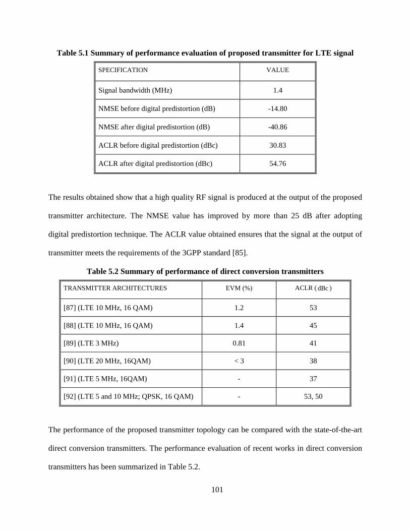
Table 5.1 Summary of performance evaluation of proposed transmitter for LTE signal
SPECIFICATION VALUE
Signal bandwidth (MHz) 1.4
NMSE before digital predistortion (dB) -14.80
NMSE after digital predistortion (dB) -40.86
ACLR before digital predistortion (dBc) 30.83
ACLR after digital predistortion (dBc) 54.76
The results obtained show that a high quality RF signal is produced at the output of the proposed
transmitter architecture. The NMSE value has improved by more than 25 dB after adopting
digital predistortion technique. The ACLR value obtained ensures that the signal at the output of
transmitter meets the requirements of the 3GPP standard [85].
Table 5.2 Summary of performance of direct conversion transmitters
TRANSMITTER ARCHITECTURES EVM (%) ACLR ( dBc )
[87] (LTE 10 MHz, 16 QAM) 1.2 53
[88] (LTE 10 MHz, 16 QAM) 1.4 45
[89] (LTE 3 MHz) 0.81 41
[90] (LTE 20 MHz, 16QAM) < 3 38
[91] (LTE 5 MHz, 16QAM) - 37
[92] (LTE 5 and 10 MHz; QPSK, 16 QAM) - 53, 50
The performance of the proposed transmitter topology can be compared with the state-of-the-art
direct conversion transmitters. The performance evaluation of recent works in direct conversion
transmitters has been summarized in Table 5.2.
101

The performance of these topologies can vary with the design specifications and the field of
application. These measurement results are for different signal bandwidths and for different
modulation schemes of the LTE signal. Some of these architectures were designed for higher
output power and have driver amplifiers integrated. Few of them target higher bandwidth and
few architectures target integration capability.
Hence, in this thesis work for comparison purposes a calibrated, high performance signal
generator (ESG 4438C from Agilent Technologies), which offers optimum performance is used.
The same LTE signal used for the evaluation of transmitter is downloaded into the generator and
the RF signal output is captured using spectrum analyzer. The baseband signal from VSA
software is compared to the original complex signal. The measurement results are summarized in
Table 5.3.
Table 5.3 Performance evaluation of signal generator for LTE signal
SPECIFICATION VALUE
Signal bandwidth (MHz) 1.4
NMSE from signal generator (dB) -43.56
ACLR (dBc) 66.62
The reduction in the NMSE value of the signal at the output of proposed transmitter as compared
to that of signal generator can be attributed to the following impairments. The signal
decomposition introduces distortion due to filtering and offset addition. The addition of DC
offset results in variation of power levels of the components with respect to the complex signal
power and affects NMSE values. The predistorted signals at the output of DPD models have
residual phases, which are approximated to zero. These approximations will reduce the NMSE
value of the signal obtained after power combining. Also, the VGAs introduce noise into the RF
102

signal and increase the noise floor of the system. This distortion reduces the dynamic range of
the architecture and the ACLR values as compared to the signal generator performance.
Figure 5.12. LTE signal spectrum at the output of transmitter.
The spectral response of the LTE signal obtained after recombination is shown in Fig. 5.12. The
distortion in the signal is reduced through predistortion. The proposed transmitter has no
emissions over a wide frequency range and does not require any filtering at the output. The
VGAs operate over a wide frequency range and thus the proposed transmitter offers large RF
bandwidth and reconfigurability. The input-output envelope and phase responses of the
transmitter architecture are shown in Fig. 5.13 and Fig. 5.14, respectively. The envelope and
phase responses are linearized after adopting digital predistortion technique using memory
polynomial modelling.
103

Figure 5.13. Input-output envelope response of the proposed transmitter.
Figure 5.14. Input-output phase response of the proposed transmitter.
104
5.10 Conclusion
In this chapter, a new transmitter architecture, the three-way amplitude modulation-based
transmitter, using only envelope modulators was proposed. Three VGAs acting as envelope
modulators were utilized to realise this architecture. A three-coordinate signal decomposition
algorithm, which incorporates the phase error from the VGAs, was used. The nonlinear phase
and amplitude response of the VGAs introduced significant distortion to the signal obtained after
recombination. A new calibration technique was used to mitigate the gain and phase
imperfections in the VGA in each of the three paths. A memory polynomial was used to model
the response of each of the VGAs. The proposed architecture and the proposed calibration
technique were tested using a LTE signal. The NMSE of the LTE signal obtained after
recombination as compared to the original complex signal was improved from -15 dB to -41 dB
using digital predistortion technique. The ACLR was improved to 55 dBc and ensured that the
signal at the output of transmitter met the standard ACLR requirements.
The new transmitter architecture translates the baseband IQ signal to RF without using a mixer,
up-converter circuits and phase modulators. As a result, the proposed transmitter does not have
any spurious emissions and does not require any filtering at the output. The large RF bandwidth
of the VGAs and the absence of filters make the design more reconfigurable than conventional
topologies.
105

Conclusion and Future Work Chapter Six:
The importance of multi-standard and reconfigurable transmitters has been established in this
thesis work. To meet the demands of modern wireless communications signals with complex
modulation schemes, multi-standard and reconfigurable transmitters are needed. RFDACs are
promising candidates for direct-digital transmitter topologies with better reconfigurability.
RFDACs enable the direct conversion of digital baseband signal to analog RF signal by
combining the DAC and the mixer. RFDAC based transmitters help in reducing the chip area by
eliminating analog blocks; reconstruction filters and VGAs. Several architectures based on
RFDACs have been proposed and different techniques are adopted in them to reduce the DAC
emissions. The emissions from mixers and DACs and the filtering techniques used to reduce
them, prevent these transmitter topologies from realising their full scale advantages. The use of
band-limited filters limits the reconfigurability and increases the footprint of these topologies.
Also, the usage of multiple filters prevents the transmitter design from being integrable.
In this thesis work, transmitter architectures, which avoid mixers/quadrature up-converters and
phase modulator circuits have been proposed and investigated. These transmitter topologies are
realised using envelope and phase modulators.
The polar decomposition of complex IQ signal results in amplitude and phase components with
higher bandwidths. The huge bandwidth and discontinuities in the phase component force the use
of IQ modulators for frequency up-conversion.
New polar transmitter architecture has been proposed using a VGA as an envelope modulator,
and a phase shifter as phase modulator. This architecture avoided the use of traditional up-
converters for frequency up-conversion. VGAs are good candidates for envelope modulators
with the bandwidth of the gain control port as the limiting factor. 106
Phase shifters offer an alternative way of phase signal up-conversion with reduced complexity
and help avoiding PLL circuits and IQ modulators for phase signal up-conversion. Signal
conditioning has been applied to avoid phase discontinuities and to reduce the bandwidth of
phase signals. This conditioning, involved adding a dc shift to the complex signal constellation.
This addition of dc component is compensated at the output of the modulator by using a multi-
branch topology. The nonlinearity and memory effects exhibited by the devices cause amplitude
and phase distortions and deteriorate the output signal quality. This nonlinearity in the devices
requires pre-compensation. Digital predistortion technique has been used to mitigate the
imperfections. New calibration technique was proposed and validated in this work. This new
technique offered better modelling results as compared to conventional memory polynomial
predistortion. The EVM measurements performed ensure the adherence of output signal quality
to the requirements of the LTE communication standard. However, the phase noise from the
phase shifter limited the quality of the transmitter output signal.
Another transmitter topology, the three-way amplitude modulation-based transmitter, was
proposed to avoid the phase modulator circuits. The absence of phase component nullified the
issues of bandwidth expansion and phase discontinuity in phase modulated signals. This
architecture was realised using envelope modulators based on the principle of three-coordinate
decomposition of signals. Digital predistortion technique was used to mitigate the imperfections
in the VGAs. The measurements performed using LTE signals and the low values of error
obtained, ensured the high quality performance of the architecture and the calibration technique.
The spectral quality of the RF signals at the output of the two proposed transmitter architectures
were evaluated using ACLR measurements. The ACLR of LTE signals at the output of the
transmitters conformed to the requirements of the LTE signal standard.
107

The wideband spectral response of the proposed architectures shows that they have very low
spurious emissions and do not require any filtering at the RF output. Also, the wide frequency
range of operation of the devices offers large RF bandwidth for the proposed architectures. The
absence of band limiting filters has made these transmitter designs a step closer to reconfigurable
radios.
6.1 Summary of contributions
The contributions of this thesis work are
I. A phase modulation architecture using an analog phase shifter was proposed in this work.
The phase shifter up-converts the baseband phase component to RF domain. A signal
conditioning method was proposed to reduce phase discontinuities during this
implementation. The proposed conditioning method and the measurement results have
been summarized and submitted in a conference proceeding.
S.Illath and M. Helaoui, “Signal conditioning for mixerless all-digital OFDM
wireless transmitters”, IEEE DCAS, 2014, accepted.
II. Mixerless polar modulator-based transmitter architecture was proposed using a
combination of a VGA as an envelope modulator, and a phase shifter as a phase
modulator. A new calibration technique was proposed in this work to model the
imperfections and digital predistortion technique was used to linearize the response. The
theory of operation, implementation and performance evaluation of this transmitter
architecture have been summarized and submitted in a peer reviewed journal.
S.Illath and M. Helaoui, “New polar modulator-based mixerless wireless
transmitter suitable for high integration and reconfigurability”, IEEE Trans.
Circuits and Systems, 2014, submitted. 108

III. A new transmitter architecture using three-way amplitude modulation has been proposed
in this thesis work. Three variable gain amplifiers act as envelope modulators and
translate the baseband IQ complex signal to RF without using mixers and phase
modulator circuits. The research findings have been summarized and submitted in a peer
reviewed journal.
S.Illath and M. Helaoui, “Highly linear and highly reconfigurable three-way
amplitude modulation-based mixerless wireless transmitter”, IEEE Trans.
Microwave. Theory Tech., 2014, submitted.
6.2 Future work
Research activities that can be carried out as an extension to this thesis include;
I. The polar transmitter architecture implemented using VGA and phase shifter has issues
with phase noise and introduces significant distortion to the output signal as described in
chapter four. The phase noise from the shifter cannot be modelled and compensated. New
phase shifters with better phase noise profile can be explored and tested. The
discontinuities in the phase component were avoided using the proposed signal
conditioning method. The addition of DC was compensated using multi-branch topology.
Exploring and analyzing new methods to reduce the bandwidth expansion and to reduce
the phase discontinuities can be included as extension to this thesis work. PLL circuits
with wide bandwidth and reduced signal processing complexity can be explored for phase
modulator circuit implementation.
II. Complete hardware implementation of the proposed transmitter topology using three
envelope modulators. This includes design and implementation of the three-way power
109

combiner/divider and the phase rotation elements using microstrip transmission lines.
The Scattering parameters of these passive components will be measured and
characterized. The reduction in NMSE value of signal at the output of proposed
transmitter as compared to that of signal generator and the impairments causing this
reduction, were discussed in chapter five. Better signal decomposition techniques can be
explored which will avoid the filtering and offset requirements. Also, the designed
passive components will have a frequency response which needs to be characterized. The
designed passive components will exhibit phase offsets which may result in signal
distortion at the transmitter output. These impairments should be compensated to ensure a
high quality signal at the output. Efforts can be made to develop new calibration
techniques to compensate these impairments from the passive components and the
envelope modulators together. New modelling techniques can be used to linearize the
phase response of VGAs and to avoid phase approximations. Once the passive
components and modulators are put together, each component path will have different
time delays and these need to be adjusted for accurate recombination of the three
components.
110

References
[1] Motorola, “Wireless network healthcare solutions,” white paper-Motorola, 2010.
[2] Rysavy Research, “Mobile broadband explosion,” white paper-Rysavy Research, 2012.
[3] G. Punz, “Evolution of 3G networks,” Springer Wien, pp. 21, 2010.
[4] Ericsson, “Long term evolution (LTE): An introduction,” white paper-Ericsson, 2011.
[5] NSN, “The advanced LTE toolbox for more efficient delivery of better user experience,” White paper-Nokia Siemens Networks, 2011.
[6] J. Mitola, “The software radio architecture,” IEEE Communications Magazine, vol. 33, pp. 26-38, 1995.
[7] E. Grayver, “Implementing software defined radio,” Springer, 2013.
[8] Quezen. Gu, “RF system design of transceivers for wireless communications,” Springer, pp. 311, 2005.
[9] J. G. Freed, “Equations provide accurate third-order IMD analysis,” Microwaves & RF, pp. 75-84, August 1992.
[10] M. D. McKinley, K. A. Remley, M. Myslinski, J. S. Kenney, D. Schreurs and B. Nauwelaers, “EVM calculation for broadband modulated signals,” in proc. of 64th ARFTG Conf., pp. 45-52, 2004.
[11] Agilent Technologies, “Measuring ACLR performance in LTE transmitters,” Application note-Agilent Technologies, 2010.
[12] Anritsu, “LTE resource guide,” Application Note Anritsu, 2009.
[13] N. Zimmermann, “Design and implementation of a broadband RF-DAC transmitter for wireless communications,” Thesis RWTH Aachen University, 2011.
[14] M. R. Sadeghifar and J. Wikner, “A survey of RF DAC architectures,” in proc. of Swedish System on Chip Conference, 2010.
[15] Current RF, “The RFDAC (radio frequency digital to analog converter) breakthrough and advantages,” White Paper-Current RF, 2004.
[16] S. Luschas, R. Schreier and H.S Lee, “Radio frequency digital-to-analog converter,” IEEE J. Solid-State Circuits, vol. 39, pp. 1462-1467, 2004.
111

[17] Y. Zhou and J. Yuan, “A 10-bit wide-band CMOS direct digital RF amplitude modulator, ”IEEE J. Solid-State Circuits, vol. 38, pp. 1182-1188, 2003.
[18] Barrie Gilbert, “A precise four-quadrant multiplier with sub-nanosecond response,” IEEE J. Solid-State Circuits, vol. 3, pp. 365-373, 1968.
[19] P. Eloranta, P. Seppinen and A. Parssinen, “Direct-digital RF-modulator: a multi-function architecture for a system-independent radio transmitter,” IEEE Comm. Magazine, vol. 46, pp. 144-151, 2008.
[20] S.M.Taleie, T.Copani, B. Bakkaloglu and S. Kiaei, “A linear ΣΔ digital IF to RFDAC transmitter with embedded mixer,” IEEE Trans. Microwave Theory and Tech., vol. 56, pp. 1059-1068, 2008.
[21] A.Jerng, “Delta-sigma digital-RF modulation for high data rate transmitters,” Thesis Massachusetts Institute of Technology, 2007.
[22] P. Eloranta, P. Seppinen, S. Kallioinen, T. Saarela and A. Parssinen, “A multimode transmitter in 0.13 μm CMOS using direct-digital RF modulator,” IEEE J. Solid-State Circuits, vol. 42, pp. 2774-2784, 2007.
[23] M. S. Alavi, R. B. Staszewski, L. C. N. de Vreede, A. Visweswaran and J. R. Long, “All-digital RF modulator,” IEEE Trans. Microwave Theory and Tech., vol. 60, pp. 3513-3526, 2012.
[24] L. R. Kahn, “Single-sideband transmission by envelope elimination and restoration,” in proc. of IRE, vol. 40, pp. 803-806, 1952.
[25] J. Groe, “Polar transmitters for wireless communications,” IEEE Comm. Magazine, vol. 45, pp. 58-63, 2007.
[26] Grebennikov, Andrei Sokal, Nathan O. Franco and Marc J, “Switch-mode RF and microwave power amplifiers,” Academic Press, 2012.
[27] D. Rudolph, “Out-of-band emissions of digital transmissions using Kahn EER technique,” IEEE Trans. Microwave Theory and Tech., vol. 50, pp. 1979-1983, 2002.
[28] J. Lopez, Y. Li, J. D. Popp, D. Y. Lie, C. C. Chuang, K. Chen, S. Wu, T. Yin Yang and G. K. Ma, “Design of highly efficient wideband RF polar transmitters using the envelope-tracking technique,” IEEE J. Solid-State Circuits, vol. 44, pp. 2276-2294, 2009.
[29] Y. Li, J. Lopez, D. Y. Lie, K. Chen, S. Wu, T. Yi Yang and G. K. Ma, “Circuits and system design of RF polar transmitters using envelope-tracking and SiGe power amplifiers for mobile WiMAX,” IEEE Trans. Circuits and Systems I: Regular Papers, vol. 58, pp. 893-901, 2011.
[30] N. B. de Carvalho and J. C. Pedro, “A comprehensive explanation of distortion sideband asymmetries,” IEEE Trans. Microwave Theory and Tech, vol. 50, pp. 2090-2101, 2002.
112

[31] J. Choi, D. Kim, D. Kang and B. Kim, “A polar transmitter with CMOS programmable hysteretic-controlled hybrid switching supply modulator for multi-standard applications,” IEEE Trans. Microwave Theory and Tech., vol. 57, pp. 1675-1686, 2009.
[32] J. Jeong, D. F. Kimball, M. Kwak, P. Draxler and P. M. Asbeck, “Envelope tracking power amplifiers with reduced peak-to-average power ratio RF input signals,” in proc. of IEEE Radio and Wireless Symposium, pp. 112-115, 2010.
[33] A. Kavousian, D.K. Su, M. Hekmat, A. Shirvani and B. Wooley, “A digitally modulated polar CMOS power amplifier with a 20-MHz channel bandwidth,” IEEE J. Solid-State Circuits, vol. 43, pp.2251-2258, 2008.
[34] Min Park, M. H. Perrott and R. B. Staszewski, “A time-domain resolution improvement of an RF-DAC,” IEEE Trans. Circuits and Systems II: Express Briefs, vol. 57, pp. 517-521, 2010.
[35] C. D. Presti, F. Carrara, A. Scuderi, P. M. Asbeck and G. Palmisano, “A 25 dBm digitally modulated CMOS power amplifier for WCDMA/EDGE/OFDM with adaptive digital predistortion and efficient power control,” IEEE J. Solid-State Circuits, vol. 44, pp. 1883-1896, 2009.
[36] T. M. van Zeijl Paul and M. Collados, “A multi-standard digital envelope modulator for polar transmitters in 90nm CMOS,” in proc. of IEEE Radio Frequency Integrated Circuits Symposium, pp. 373-376, 2007.
[37] J. H. Chen, H. S. Yang, H. C. Lin and Y.E. Chen, “A polar transmitter architecture using multiphase pulsewidth modulation,” IEEE Trans. Circuits and Systems I: Regular Papers, vol. 58, pp. 244-252, 2011.
[38] H. S. Yang and Y. E. Chen, “A polar transmitter using interleaving pulse modulation for multimode handsets,” IEEE Trans. Microwave Theory and Tech., vol. 59, pp. 2083-2090, 2011.
[39] M. R. Elliott, T. Montalvo, B. P. Jeffries, F. Murden, J. Strange, A. Hill, S. Nandipaku and J. Harrebek, “A polar modulator transmitter for GSM/EDGE,” IEEE J. Solid-State Circuits, vol. 39, pp. 2190-2199, 2004.
[40] M. Ito, T. Yamawaki, M. Kasahara and S. Williams, “Variable gain amplifier in polar loop modulation transmitter for EDGE,” in proc. of European solid-state circuits conference, pp. 511-514, 2005.
[41] A.M. Niknejad, D. Chowdhury and J. Chen, “Design of CMOS power amplifiers,” IEEE Trans. Microwave Theory and Tech., vol. 60, pp. 1784-1796, 2012.
[42] L. Ye, J. Chen, L. Kong, E. Alon and A. M. Niknejad, “Design considerations for a direct digitally modulated WLAN transmitter with integrated phase path and dynamic impedance modulation,” IEEE J. Solid-State Circuits, vol. 48, pp. 3160-3177, 2013.
113

[43] R. B. Staszewski, J. L. Wallberg, S. Rezeq, C. M. Hung, O. E. Eliezer, S. K. Vemulapalli, C. Fernando, K. Maggio, R. Staszewski, N. Barton, M. C. Lee, P. Cruise, M. Entezari, K. Muhammad and D. Leipold, “All-digital PLL and transmitter for mobile phones, ” IEEE J. Solid-State Circuits, vol. 40, pp. 2469-2482, 2005.
[44] Y. C. Jeong, “Design of a novel vector modulator,” Microwave Journal, vol. 44, pp.156-162, 2011.
[45] GT Microwave, “Phase shifters, vector modulators, delay-lines and frequency translators,” Application Note.
[46] M. Goldfarb, J. B. Cole and A. Platzker, “A novel MMIC bi-phase modulator with variable gain using enhancement-mode FETS suitable for 3 V wireless applications,” in proc. of IEEE Microwave and Millimeter-Wave Monolithic Circuits Symposium, pp. 99-102, 1994.
[47] G. B. Norris, D. C. Boire, G. St.Onge, C. Wutke, C. Barratt, W. Coughlin and J. Chickanosky, “A fully monolithic 4-18 GHz digital vector modulator,” IEEE MTT symposium, pp. 789-792 vol.2, 1990.
[48] R. Pyndiah, P. Jean, R. Leblanc and J. Meunier, “GaAs monolithic direct linear (1-2.8) GHz Q.P.S.K. modulator,” in proc. of EuMC, pp. 597-602, 1989.
[49] P. Tosovsky and D. Valunch, “Improvement of RF vector modulator performance by feed-forward based calibration,” Radio Eng., vol. 19, 2010.
[50] D. Tuite, “Design variable gain amplifier FAQs,” Application Note, Analog Devices.
[51] A. K. Das and M. Frechette, “An RF variable gain amplifier with linear-in-dB gain steps and automatic power consumption optimization,” IEEE Dallas Workshop on CAS, pp. 1-4, 2009.
[52] B. Gilbert, “Translinear circuits: a proposed classification,” IEEE Electronics Letters, vol. 11, pp. 14-16, 1975.
[53] Analog Devices, “High speed variable gain amplifiers (VGAs),” Application Note-Analog Devices Inc., 2009.
[54] H. Zumbahlen, “Basic linear design,” Application Note-Analog Devices Inc., 2007.
[55] N. Boulejfen, A. Harguem, O. Hammi, F. M. Ghannouchi and A. Gharsallah, “Analytical prediction of spectral regrowth and correlated and uncorrelated distortion in multicarrier wireless transmitters exhibiting memory effects,” IET Microwaves, Antennas & Propagation, vol. 4, pp. 685-696, 2010.
[56] D. Schreurs, M. O. Droma, A. A. Goacher and M. Gadringer, “RF Power Amplifier Behavioral Modeling,” Artech House, 2009.
114

[57] H. Ku and J. S. Kenney, “Behavioral modeling of nonlinear RF power amplifiers considering memory effects,” IEEE Trans. Microwave Theory and Tech., vol. 51, pp. 2495-2504, 2003.
[58] L. Ding, G. T. Zhou, D. R. Morgan, Zhengxiang Ma, J. S. Kenney, Jaehyeong Kim and C. R. Giardina, “A robust digital baseband predistorter constructed using memory polynomials, ” IEEE Trans. Communications, vol. 52, pp. 159-165, 2004.
[59] F.M. Ghannouchi and O. Hammi, “Behavioral modeling and predistortion,” IEEE Microwave Magazine, vol.10, pp.52-64, 2009.
[60] E. Arabi and S. Ali, “Behavioral modeling of RF frond end devices in Simulink,” Thesis, 2008.
[61] S. Ghadrdan, M. Ahmadian, S. Salari and M. Heydarzadeh, “An improved blind channel estimation algorithm for OFDM systems,” in proc. of in international symposium in Telecommunications (IST), pp. 421-425, 2010.
[62] L. Tee, E. Sacchi, R. Bocock, N. Wongkomet and P. R. Gray, “A cartesian-feedback linearized CMOS RF transmitter for EDGE modulation,” in proc. of Symposium on in VLSI Circuits, pp. 232-233, 2006.
[63] T. Sowlati, Y. Greshishchev, C. A. T. Salama, G. Rabjohn and J. Sitch, “Linear transmitter design using high efficiency class E power amplifier,” in proc. of IEEE symposium PIMRC, pp. 1233,1995.
[64] F. Ellinger, “Radio Frequency Integrated Circuits and Technologies,” Springer, 2007.
[65] R. N. Alcock, “Phase control of pulsed broadband microwave amplifiers,” in proc. of IEEE Comm. Radar and Signal Processing, vol. 129, pp. 447-451, 1982.
[66] H. M. Park, D. H. Baek, K. Jeon, J. W. Moon and S. Hong, “A new predistortion linearizer using envelope-feedback technique for PCS high power amplifier application,” in proc. of IEEE Radio and Wireless Conference, pp. 223-226, 1999.
[67] S. S. Singh, “Design and realization of S-band GaAs MMIC two bit phase shifter for phase array radar antenna applications,” in proc. of Recent Advances in Microwave Theory and Applications, pp. 574-577, 2008.
[68] L. G. Maloratsky, “Electrically tunable switched-line diode phase shifters,” High Frequency Electronics, 2010.
[69] Alpha, “Design with PIN diodes,” Alpha-Application Note.
[70] Skyworks Solutions, “A varactor controlled phase shifter for PCS base station applications,” Application note-Skyworks Solutions Inc, 2009.
115
[71] D. Rudolph, “Out-of-band emissions of digital transmissions using Kahn EER technique,” IEEE Trans. Microwave Theory and Tech., vol. 50, pp. 1979-1983, 2002.
[72] W. Loke, M. Y. Chia and P. Chee, “Design considerations for multi-band OFDM polar transmitter of UWB system,” IEEE Electronics Letters, vol. 43, 2007.
[73] M. Talonen and S. Lindfors, “System requirements for OFDM polar transmitter,” in proc. of IEEE European Conference on Circuit Theory and Design, pp. III/69-III/72 vol. 3,2005.
[74] J. Zhuang, K. Waheed and R. B. Staszewski, “A technique to reduce phase/frequency modulation bandwidth in a polar RF transmitter,” IEEE Trans. Circuits and Systems I: Regular Papers, vol. 57, pp. 2196-2207, 2010.
[75] J. Wang, A. Zhu, X. Zhu and T. J. Brazil, “Vector hole punching technique for OFDM signals using circle-tangent shift and unused tones,” IEEE Trans. Microwave Theory and Tech., vol. 57, pp. 2682-2691, 2009.
[76] A. K. Mustafa and M. Faulkner, “Theoretical analysis of hole punch signal conditioning for high efficiency EER power amplifiers,” EURASIP J. Wireless Communications and Networking, 2010.
[77] H. Zhu, M. Ding and Y. Li, “Gibbs phenomenon for fractional Fourier series,” in proc. of IET Signal Processing, vol. 5, pp. 728-738, 2011.
[78] S. C. Thompson, A. Ahmed, J. G. Proakis, J. R. Zeidler and M. J. Geile, “Constant envelope OFDM,” IEEE Trans. Comm., vol. 56, pp. 1300-1312, 2008.
[79] M. Gdeisat and F. Lilley, “One-dimensional phase unwrapping problem,” Application note, 2012.
[80] Actel, “Improving ADC results,” Application note-Actel, 2007.
[81] Agilent Technologies, “De-emphasized signal generation with the Agilent 81250A ParBERT,” Application Note-Agilent Technologies, USA, 2009.
[82] Anritsu, “Ideal pre-emphasis constant setting,” Application Note-Anritsu, Japan, 2011.
[83] Cheh. Pan, “Gibbs phenomenon removal and digital filtering directly through the fast Fourier transform,” IEEE Trans. Signal Processing, vol. 49, pp. 444-448, 2001.
[84] J. L. Arrowood and M. J. T. Smith, “Gibbs phenomenon suppression using fir time-varying filter banks, ” in proc. of Digital Signal Processing Workshop, pp. 2.1.1-2.1.2, 1992.
[85] 3GPP TS 36.104-LTE; evolved universal terrestrial radio access (E-UTRA); base station (BS) radio transmission and reception technical standard, 3rd Generation Partnership Project, (2012-11).
116

[86] Robert Blitzer, “Precalculus Essentials.” Prentice-Hall, Inc., pp. 639-643, 2007.
[87] M. Collados, H. Zhang, B. Tenbroek and H. Chang, “A low-current digitally predistorted direct-conversion transmitter with 25% duty-cycle passive mixer,” IEEE Trans. Microwave Theory and Tech., vol. 62, pp. 726-731, 2014.
[88] P. Rossi, N. Codega, D. Gerna, A. Liscidini, D. Ottini, Yong He, A. Pirola, E. Sacchi, G. Uehara, C. Yang and R. Castello, “An LTE transmitter using a class-A/B power mixer,” in proc. of digest of technical Papers ISSCC, pp. 340-341, 2013..
[89] O. Oliaei, M. Kirschenmann, D. Newman, K. Hausmann, Haolu Xie, P. Rakers, M. Rahman, M. Gomez, Chuanzhao Yu, B. Gilsdorf and K. Sakamoto, “A multiband multimode transmitter without driver amplifier, ” in proc. of digest of technical Papers ISSCC, pp. 164-166, 2012.
[90] S. Fukuda, S. Miya, M. Io, K. Hamashita and B. Nauta, “Direct-digital modulation (DIDIMO) transmitter with −156dBc/hz rx-band noise using FIR structure,” in proc. of ESSCIRC, pp. 53-56, 2012.
[91] S. Shim, H. Y. Lee, J. H. Choi, H. K. Yu and S. Hong, “Digital-RF transmitter for wireless communication in 90nm CMOS, ” in proc. of IMWS-IRFPT, pp. 1-2, 2011.
[92] M. Collados, H. Zhang, B. Tenbroek and H. Chang, “A low-current digitally predistorted 3G-4G transmitter in 40nm CMOS,” in proc. of IEEE RFIC symposium, pp. 141-144, 2013.
117