mips32® 1074k™ cpu family software user’s manual
TRANSCRIPT

Document Number: MD00749Revision 01.03June 03, 2011
MIPS32® 1074K™ CPU Family SoftwareUser’s Manual

Unpublished rights (if any) reserved under the copyright laws of the United States of America and other countries. This document contains information that is proprietary to MIPS Tech, LLC, a Wave Computing company (“MIPS”) and MIPS’ affiliates as applicable. Any copying, reproducing, modifying or use of this information (in whole or in part) that is not expressly permitted in writing by MIPS or MIPS’ affiliates as applicable or an authorized third party is strictly prohibited. At a minimum, this information is protected under unfair competition and copyright laws. Violations thereof may result in criminal penalties and fines. Any document provided in source format (i.e., in a modifiable form such as in FrameMaker or Microsoft Word format) is subject to use and distribution restrictions that are independent of and supplemental to any and all confidentiality restrictions. UNDER NO CIRCUMSTANCES MAY A DOCUMENT PROVIDED IN SOURCE FORMAT BE DISTRIBUTED TO A THIRD PARTY IN SOURCE FORMAT WITHOUT THE EXPRESS WRITTEN PERMISSION OF MIPS (AND MIPS’ AFFILIATES AS APPLICABLE) reserve the right to change the information contained in this document to improve function, design or otherwise. MIPS and MIPS’ affiliates do not assume any liability arising out of the application or use of this information, or of any error or omission in such information. Any warranties, whether express, statutory, implied or otherwise, including but not limited to the implied warranties of merchantability or fitness for a particular purpose, are excluded. Except as expressly provided in any written license agreement from MIPS or an authorized third party, the furnishing of this document does not give recipient any license to any intellectual property rights, including any patent rights, that cover the information in this document. The information contained in this document shall not be exported, reexported, transferred, or released, directly or indirectly, in violation of the law of any country or international law, regulation, treaty, Executive Order, statute, amendments or supplements thereto. Should a conflict arise regarding the export, reexport, transfer, or release of the information contained in this document, the laws of the United States of America shall be the governing law. The information contained in this document constitutes one or more of the following: commercial computer software, commercial computer software documentation or other commercial items. If the user of this information, or any related documentation of any kind, including related technical data or manuals, is an agency, department, or other entity of the United States government ("Government"), the use, duplication, reproduction, release, modification, disclosure, or transfer of this information, or any related documentation of any kind, is restricted in accordance with Federal Acquisition Regulation 12.212 for civilian agencies and Defense Federal Acquisition Regulation Supplement 227.7202 for military agencies. The use of this information by the Government is further restricted in accordance with the terms of the license agreement(s) and/or applicable contract terms and conditions covering this information from MIPS Technologies or an authorized third party. MIPS, MIPS I, MIPS II, MIPS III, MIPS IV, MIPS V, MIPSr3, MIPS32, MIPS64, microMIPS32, microMIPS64, MIPS-3D, MIPS16, MIPS16e, MIPS-Based, MIPSsim, MIPSpro, MIPS-VERIFIED, Aptiv logo, microAptiv logo, interAptiv logo, microMIPS logo, MIPS Technologies logo, MIPS-VERIFIED logo, proAptiv logo, 4K, 4Kc, 4Km, 4Kp, 4KE, 4KEc, 4KEm, 4KEp, 4KS, 4KSc, 4KSd, M4K, M14K, 5K, 5Kc, 5Kf, 24K, 24Kc, 24Kf, 24KE, 24KEc, 24KEf, 34K, 34Kc, 34Kf, 74K, 74Kc, 74Kf, 1004K, 1004Kc, 1004Kf, 1074K, 1074Kc, 1074Kf, R3000, R4000, R5000, Aptiv, ASMACRO, Atlas, "At the core of the user experience.", BusBridge, Bus Navigator, CLAM, CorExtend, CoreFPGA, CoreLV, EC, FPGA View, FS2, FS2 FIRST SILICON SOLUTIONS logo, FS2 NAVIGATOR, HyperDebug, HyperJTAG, IASim, iFlowtrace, interAptiv, JALGO, Logic Navigator, Malta, MDMX, MED, MGB, microAptiv, microMIPS, Navigator, OCI, PDtrace, the Pipeline, proAptiv, Pro Series, SEAD-3, SmartMIPS, SOC-it, and YAMON are trademarks or registered trademarks of MIPS and MIPS’ affiliates as applicable in the United States and other countries. All other trademarks referred to herein are the property of their respective owners.
aLt{онϯ млтпYϰ /t¦ CŀƳƛƭȅ {ƻŦǘǿŀNJŜ ¦ǎŜNJΩǎ aŀƴdzŀƭΣ wŜǾƛǎƛƻƴ лмΦло

MIPS32® 1074K™ CPU Family Software User’s Manual, Revision 01.03 3

4 MIPS32® 1074K™ CPU Family Software User’s Manual, Revision 01.03
Table of Contents
Chapter 1: Introduction to the MIPS32® 1074K™ CPU Family......................................................... 251.1: 1074K™ CPU Features............................................................................................................................. 26
1.1.1: Pipeline ............................................................................................................................................ 261.1.2: Instruction Set .................................................................................................................................. 271.1.3: Memory Management, Caches, and Scratchpad Memory............................................................... 281.1.4: Interfaces ......................................................................................................................................... 291.1.5: Power Control .................................................................................................................................. 291.1.6: Debug............................................................................................................................................... 301.1.7: Other ................................................................................................................................................ 30
1.2: 1074K™ CPU Block Diagram.................................................................................................................... 301.2.1: Instruction Fetch Unit (IFU) .............................................................................................................. 321.2.2: Instruction Cache ............................................................................................................................. 331.2.3: Instruction Decode/Dispatch Unit (IDU) ........................................................................................... 331.2.4: Instruction Execution Unit (IEU) ....................................................................................................... 341.2.5: Multiply Divide Unit (MDU) ............................................................................................................... 341.2.6: CorExtend® User Defined Instructions (UDIs)................................................................................. 341.2.7: Load Store Unit (LSU)...................................................................................................................... 351.2.8: System Control Coprocessor (CP0)................................................................................................. 351.2.9: Memory Management Unit (MMU)................................................................................................... 351.2.10: Data Cache .................................................................................................................................... 361.2.11: Scratchpad RAM............................................................................................................................ 361.2.12: Graduation Unit (GRU)................................................................................................................... 361.2.13: Bus Interface Unit (BIU) ................................................................................................................. 371.2.14: Coprocessor Interface Unit (CIU)................................................................................................... 371.2.15: Power Management ....................................................................................................................... 371.2.16: EJTAG Debug................................................................................................................................ 37
Chapter 2: Pipeline of the 1074K™ CPU............................................................................................. 392.1: Integer Pipeline Description....................................................................................................................... 39
2.1.1: IFU Pipeline...................................................................................................................................... 402.1.1.1: IT - Instruction Cache Tag Access ......................................................................................... 402.1.1.2: ID - Instruction Cache Data Access........................................................................................ 412.1.1.3: IS - Instruction Select ............................................................................................................. 412.1.1.4: IR - Instruction Recode........................................................................................................... 412.1.1.5: IK - Instruction ........................................................................................................................ 412.1.1.6: IX - Instruction Macro Expansion............................................................................................ 412.1.1.7: IB - Instruction Buffer .............................................................................................................. 42
2.1.2: Instruction Decode Unit Pipeline ...................................................................................................... 422.1.2.1: DD - Dispatch Decode............................................................................................................ 422.1.2.2: DR - Dispatch Rename........................................................................................................... 422.1.2.3: DS - Dispatch Select .............................................................................................................. 422.1.2.4: DM - DDQ Mux ....................................................................................................................... 43
2.1.3: ALU Pipeline .................................................................................................................................... 432.1.3.1: AF - ALU Pipe Register File Read.......................................................................................... 432.1.3.2: AM - ALU Pipe Operand Bypass Select Mux, This stage has the final operand bypass muxesfor the ALU pipe. The functionality corresponding to this stage resides entirely in the IEU. ............... 432.1.3.3: AC - ALU Compute................................................................................................................. 43

MIPS32® 1074K™ CPU Family Software User’s Manual, Revision 01.03 5
2.1.3.4: AB - ALU Bypass.................................................................................................................... 432.1.4: MDU Pipeline ................................................................................................................................... 44
2.1.4.1: MB - Multiplier Booth Recode. ................................................................................................ 442.1.4.2: M1- M3 Multiplier Array .......................................................................................................... 442.1.4.3: M4 - Multiply Add.................................................................................................................... 44
2.1.5: AGEN Pipeline ................................................................................................................................. 442.1.5.1: EM - Execute Operand Bypass Select Mux ........................................................................... 442.1.5.2: EA - Execute and Address Generate ..................................................................................... 442.1.5.3: EC - Execute and Cache Access ........................................................................................... 452.1.5.4: ES - Execute and Cache Second ........................................................................................... 452.1.5.5: EB - Execute and Cache Data Bypass................................................................................... 45
2.1.6: GRU Pipeline ................................................................................................................................... 462.1.6.1: WB - Writeback....................................................................................................................... 462.1.6.2: GC - Graduation Commit ........................................................................................................ 46
2.2: Programming the 1074K CPU ................................................................................................................... 462.3: Hazards ..................................................................................................................................................... 46
2.3.1: Types of Hazards ............................................................................................................................. 472.3.1.1: Execution Hazards, Execution hazards are those created by the execution of one instruction,and seen by the execution of another instruction. Table 2.2 lists possible execution hazards andwhether they can be resolved via setting of the IHB bit in the CP0 Config7 register.. ....................... 482.3.1.2: Instruction Hazards, Instruction hazards are those created by the execution of one instruction,and seen by the instruction fetch of another instruction. Table 2.3 lists instruction hazards. Because thefetch unit is decoupled from the execution unit, these hazards are rather large. The use of a hazardbarrier instruction is required for reliable clearing of instruction hazards. ........................................... 49
2.3.2: Instruction Listing ............................................................................................................................. 492.3.2.1: Instruction Encoding ............................................................................................................... 50
2.3.3: Eliminating Hazards ......................................................................................................................... 50
Chapter 3: Floating-Point Unit of the 1074Kf™ CPU ......................................................................... 513.1: Features Overview .................................................................................................................................... 51
3.1.1: IEEE Standard 754 .......................................................................................................................... 523.2: Enabling the Floating-Point Coprocessor .................................................................................................. 523.3: Data Formats............................................................................................................................................. 53
3.3.1: Floating-Point Formats..................................................................................................................... 533.3.1.1: Normalized and Denormalized Numbers................................................................................ 553.3.1.2: Reserved Operand Values—Infinity and NaN ........................................................................ 553.3.1.3: Infinity and Beyond ................................................................................................................. 553.3.1.4: Signalling Non-Number (SNaN) ............................................................................................. 553.3.1.5: Quiet Non-Number (QNaN) .................................................................................................... 55
3.3.2: Fixed-Point Formats......................................................................................................................... 563.4: Floating-Point General Registers .............................................................................................................. 57
3.4.1: FPRs and Formatted Operand Layout ............................................................................................. 573.4.2: Formats of Values Used in FP Registers ......................................................................................... 573.4.3: Binary Data Transfers (32-Bit and 64-Bit) ........................................................................................ 59
3.5: Floating-Point Control Registers................................................................................................................ 603.5.1: Floating-Point Implementation Register (FIR, CP1 Control Register 0)........................................... 613.5.2: Floating-Point Condition Codes Register (FCCR, CP1 Control Register 25)................................... 623.5.3: Floating-Point Exceptions Register (FEXR, CP1 Control Register 26) ............................................ 623.5.4: Floating-Point Enables Register (FENR, CP1 Control Register 28) ................................................ 633.5.5: Floating-Point Control and Status Register (FCSR, CP1 Control Register 31)................................ 643.5.6: Operation of the FS/FO/FN Bits ....................................................................................................... 66
3.5.6.1: Flush To Zero Bit .................................................................................................................... 673.5.6.2: Flush Override Bit ................................................................................................................... 67
6 MIPS32® 1074K™ CPU Family Software User’s Manual, Revision 01.03
3.5.6.3: Flush to Nearest ..................................................................................................................... 683.5.6.4: Recommended FS/FO/FN Settings........................................................................................ 69
3.5.7: FCSR Cause Bit Update Flow.......................................................................................................... 693.5.7.1: Exceptions Triggered by CTC1 .............................................................................................. 693.5.7.2: Generic Flow .......................................................................................................................... 693.5.7.3: Multiply-Add Flow ................................................................................................................... 693.5.7.4: Cause Update Flow for Input Operands ................................................................................. 703.5.7.5: Cause Update Flow for Unimplemented Operations .............................................................. 70
3.6: Instruction Overview .................................................................................................................................. 703.6.1: Data Transfer Instructions................................................................................................................ 70
3.6.1.1: Data Alignment in Loads, Stores, and Moves ........................................................................ 713.6.1.2: Addressing Used in Data Transfer Instructions ...................................................................... 71
3.6.2: Arithmetic Instructions...................................................................................................................... 723.6.3: Conversion Instructions.................................................................................................................... 733.6.4: Formatted Operand-Value Move Instructions .................................................................................. 733.6.5: Conditional Branch Instructions ....................................................................................................... 743.6.6: Miscellaneous Instructions ............................................................................................................... 75
3.7: Exceptions ................................................................................................................................................. 753.7.1: Precise Exception Mode .................................................................................................................. 753.7.2: Exception Conditions ....................................................................................................................... 76
3.7.2.1: Invalid Operation Exception.................................................................................................... 773.7.2.2: Division By Zero Exception..................................................................................................... 773.7.2.3: Underflow Exception............................................................................................................... 783.7.2.4: Overflow Exception................................................................................................................. 783.7.2.5: Inexact Exception ................................................................................................................... 783.7.2.6: Unimplemented Operation Exception..................................................................................... 78
3.8: Pipeline and Performance ......................................................................................................................... 793.8.1: Pipeline Overview ............................................................................................................................ 79
3.8.1.1: DR Stage - Dispatch Rename ................................................................................................ 793.8.1.2: C1 - Coprocessor Interface Unit Stage 1................................................................................ 793.8.1.3: CR Stage - Coprocessor Interface Unit Queue Read............................................................. 803.8.1.4: CI Stage - Coprocessor 1 Interface ........................................................................................ 803.8.1.5: FR Stage - Decode, Register Read, and Unpack................................................................... 803.8.1.6: M1 Stage - Multiply Tree ........................................................................................................ 803.8.1.7: M2 Stage - Multiply Complete ................................................................................................ 803.8.1.8: A1 Stage - Addition First Step ................................................................................................ 803.8.1.9: A2 Stage - Addition Second and Final Step ........................................................................... 803.8.1.10: FP Stage - Result Pack ........................................................................................................ 813.8.1.11: FW Stage - Register Write.................................................................................................... 81
3.8.2: Bypassing......................................................................................................................................... 813.8.3: Repeat Rate and Latency ................................................................................................................ 81
Chapter 4: The MIPS® DSP Application-Specific Extension to the MIPS32® Instruction Set....... 834.1: Additional Register State for the DSP ASE ............................................................................................... 83
4.1.1: HI-LO Registers ............................................................................................................................... 834.1.2: DSP Control Register....................................................................................................................... 83
4.2: Software Detection of the DSP ASE Revision 2........................................................................................ 85
Chapter 5: Memory Management of the 1074K™ CPU...................................................................... 875.1: Introduction................................................................................................................................................ 875.2: Modes of Operation ................................................................................................................................... 89
5.2.1: Virtual Memory Segments................................................................................................................ 895.2.1.1: Unmapped Segments............................................................................................................. 90

MIPS32® 1074K™ CPU Family Software User’s Manual, Revision 01.03 7
5.2.1.2: Mapped Segments ................................................................................................................. 915.2.2: User Mode........................................................................................................................................ 915.2.3: Supervisor Mode.............................................................................................................................. 925.2.4: Kernel Mode..................................................................................................................................... 94
5.2.4.1: Kernel Mode, User Space (kuseg) ......................................................................................... 965.2.4.2: Kernel Mode, Kernel Space 0 (kseg0).................................................................................... 965.2.4.3: Kernel Mode, Kernel Space 1 (kseg1).................................................................................... 965.2.4.4: Kernel Mode, Kernel/Supervisor Space 2 (ksseg/kseg2) ....................................................... 975.2.4.5: Kernel Mode, Kernel Space 3 (kseg3).................................................................................... 97
5.2.5: Debug Mode..................................................................................................................................... 975.2.5.1: Debug Mode, Register (drseg) ............................................................................................... 985.2.5.2: Debug Mode, Memory (dmseg).............................................................................................. 98
5.3: Translation Lookaside Buffer..................................................................................................................... 995.3.1: Joint TLB.......................................................................................................................................... 995.3.2: Instruction TLB............................................................................................................................... 101
5.4: Virtual-to-Physical Address Translation................................................................................................... 1025.4.1: Hits, Misses, and Multiple Matches................................................................................................ 1035.4.2: Memory Space............................................................................................................................... 104
5.4.2.1: Page Sizes ........................................................................................................................... 1045.4.2.2: Replacement Algorithm ........................................................................................................ 104
5.4.3: TLB Instructions ............................................................................................................................. 1055.5: Fixed Mapping MMU ............................................................................................................................... 106
Chapter 6: Exceptions and Interrupts in the 1074K™ CPU ............................................................ 1096.1: Exception Conditions............................................................................................................................... 1096.2: Exception Priority..................................................................................................................................... 1106.3: Interrupts ................................................................................................................................................. 111
6.3.1: Interrupt Modes .............................................................................................................................. 1126.3.1.1: Interrupt Compatibility Mode................................................................................................. 1126.3.1.2: Vectored Interrupt Mode....................................................................................................... 1146.3.1.3: External Interrupt Controller Mode ....................................................................................... 117
6.3.2: Generation of Exception Vector Offsets for Vectored Interrupts .................................................... 1196.3.3: Global Interrupt Controller.............................................................................................................. 120
6.4: GPR Shadow Registers........................................................................................................................... 1206.5: Exception Vector Locations ..................................................................................................................... 1226.6: General Exception Processing ................................................................................................................ 1246.7: Debug Exception Processing .................................................................................................................. 1276.8: Exception Descriptions ............................................................................................................................ 129
6.8.1: Reset Exception ............................................................................................................................. 1296.8.2: Debug Single Step Exception ........................................................................................................ 1306.8.3: Debug Interrupt Exception ............................................................................................................. 1306.8.4: Non-Maskable Interrupt (NMI) Exception....................................................................................... 1316.8.5: Machine Check Exception.............................................................................................................. 1316.8.6: Interrupt Exception ......................................................................................................................... 1326.8.7: Debug Instruction Break Exception................................................................................................ 1326.8.8: Watch Exception — Instruction Fetch or Data Access................................................................... 1336.8.9: Address Error Exception — Instruction Fetch/Data Access........................................................... 1336.8.10: TLB Refill Exception — Instruction Fetch or Data Access ........................................................... 1346.8.11: TLB Invalid Exception — Instruction Fetch or Data Access......................................................... 1346.8.12: Cache Error Exception ................................................................................................................. 1356.8.13: Bus Error Exception — Instruction Fetch or Data Access............................................................ 1366.8.14: Debug Software Breakpoint Exception ........................................................................................ 1366.8.15: Execution Exception — System Call............................................................................................ 136

8 MIPS32® 1074K™ CPU Family Software User’s Manual, Revision 01.03
6.8.16: Execution Exception — Breakpoint.............................................................................................. 1376.8.17: Execution Exception — Reserved Instruction .............................................................................. 1376.8.18: Execution Exception — Coprocessor Unusable .......................................................................... 1376.8.19: Execution Exception — CorExtend block Unusable .................................................................... 1386.8.20: Execution Exception — DSP ASE State Disabled ....................................................................... 1386.8.21: Execution Exception — Floating Point Exception ........................................................................ 1386.8.22: Execution Exception — Integer Overflow..................................................................................... 1396.8.23: Execution Exception — Trap........................................................................................................ 1396.8.24: Debug Data Break Exception....................................................................................................... 1396.8.25: TLB Modified Exception — Data Access ..................................................................................... 140
6.9: Exception Handling and Servicing Flowcharts ........................................................................................ 140
Chapter 7: CP0 Registers of the 1074K™ CPU ................................................................................ 1477.1: CP0 Register Summary........................................................................................................................... 1477.2: CP0 Register Descriptions ...................................................................................................................... 152
7.2.1: Index (CP0 Register 0, Select 0): Index into TLB array ................................................................. 1537.2.2: Random (CP0 Register 1, Select 0): Randomly Generated Index into the TLB Array................... 1547.2.3: EntryLo0-1 (CP0 Registers 2 and 3, Select 0): Output (physical) side of TLB entry...................... 1547.2.4: Context (CP0 Register 4, Select 0): Mixture of Pre-programmed and BadVAddr Bits which can act asan OS Page Table Pointer. ...................................................................................................................... 1567.2.5: ContextConfig Register (CP0 Register 4, Select 1) ....................................................................... 1577.2.6: UserLocal (CP0 Register 4, Select 2): Address Causing the Last TLB-related Exception ............ 1587.2.7: PageMask (CP0 Register 5, Select 0): Control for Variable Page Size in TLB Entries ................. 1597.2.8: Wired (CP0 Register 6, Select 0): Controls Number of Fixed ("wired") TLB Entries...................... 1607.2.9: HWREna (CP0 Register 7, Select 0): Bitmask Limiting User-mode Access to rdhwr Registers.... 1607.2.10: BadVAddr (CP0 Register 8, Select 0): Address Causing the Last TLB-related Exception .......... 1627.2.11: Count (CP0 Register 9, Select 0): Free-running Counter at Half the Pipeline Speed.................. 1627.2.12: EntryHi (CP0 Register10, Select 0): High-order Portion of TLB Entry ......................................... 1637.2.13: Compare (CP0 Register 11, Select 0): Timer Interrupt Control ................................................... 1647.2.14: Status (CP0 Register 12, Select 0): Processor Status and Control ............................................. 164
7.2.14.1: Interruptibility ...................................................................................................................... 1647.2.14.2: Operating Modes ................................................................................................................ 1657.2.14.3: Coprocessor Accessibility................................................................................................... 165
7.2.15: IntCtl (CP0 Register 12, Select 1): Setup for Interrupt Vector and Interrupt Priority Features..... 1707.2.16: SRSCtl (CP0 Register12, Select 2): Shadow Register Set Selectors.......................................... 1717.2.17: SRSMap (CP0 Register 12, Select 3): Shadow Set Choice for Each Interrupt Level in VI Mode 1737.2.18: Cause (CP0 Register 13, Select 0): Cause of Last General Exception ....................................... 1747.2.19: EPC (CP0 Register 14, Select 0): Restart Address from Exception ............................................ 1787.2.20: PRId (CP0 Register 15, Select 0): Processor Identification and Revision ................................... 1797.2.21: EBase (CP0 Register 15, Select 1): Exception entry point base address and CPU/VPE ID ....... 1807.2.22: CDMMBase Register (CP0 Register 15, Select 2)....................................................................... 1817.2.23: CMGCR Base Register (CP0 Register 15, Select 3) ................................................................... 1827.2.24: Config (CP0 Register 16, Select 0): Legacy Configuration Register............................................ 1827.2.25: Config1-2 (CP0 Register 16, Select 1-2): MIPS32/64 Configuration Registers ........................... 184
7.2.25.1: Config1 ............................................................................................................................... 1847.2.25.2: Config2 ............................................................................................................................... 185
7.2.26: Config3 (CP0 Register 16, Select 3): Configuration register showing ASEs ............................... 1867.2.27: Config6 (CP0 Register 16, Select 6) ............................................................................................ 1877.2.28: Config7 (CP0 Register 16, Select 7): CPU-specific Configuration............................................... 1907.2.29: WatchLo0-3 (CP0 Register 18, Select 0-3): Watchpoint Address and Qualifiers ........................ 1937.2.30: WatchHi0-3 (CP0 Register 19, Select 0-3): Watchpoint Control/Status....................................... 1937.2.31: Debug (CP0 Register 23, Select 0): EJTAG Debug Status/ControlRegister.................................................................................................................................................... 194

MIPS32® 1074K™ CPU Family Software User’s Manual, Revision 01.03 9
7.2.32: Trace Control Register (CP0 Register 23, Select 1) .................................................................... 1987.2.33: Trace Control2 Register (CP0 Register 23, Select 2) .................................................................. 2007.2.34: User Trace Data1 Register (CP0 Register 23, Select 3) and User Trace Data2 Register (CP0Register 24, Select 3)............................................................................................................................... 2027.2.35: TraceIBPC Register (CP0 Register 23, Select 4) ........................................................................ 2037.2.36: TraceDBPC Register (CP0 Register 23, Select 5)....................................................................... 2047.2.37: DEPC (CP0 Register 24, Select 0): Restart Address from Last EJTAG Debug Exception.......... 2057.2.38: Trace Control3 Register (CP0 Register 24, Select 2) .................................................................. 2067.2.39: PerfCtl0-3 (CP0 Register 25, Select 0, 2, 4, 6): Performance Counter Control ........................... 2077.2.40: PerfCnt0-3 (CP0 Register 25, Select 1, 3, 5, 7): Performance Counters..................................... 2127.2.41: ErrCtl (CP0 Register 26, Select 0): Software Parity Control and Test Modes for Cache RAM Arrays2127.2.42: CacheErr (CP0 Register 27, Select 0): Cache Parity Exception Status....................................... 2137.2.43: ITagLo (CP0 Register 28, Select 0): Read/write Interface for Load/Store Tag Cacheops........... 215
7.2.43.1: ITagLo (ErrCtlWST = 0, ErrCtlSPR = 0) ............................................................................. 2157.2.43.2: ITagLo-WST (ErrCtlWST = 1, ErrCtlSPR = 0) .................................................................... 2167.2.43.3: ITagLo-WST (ErrCtlWST = 0, ErrCtlSPR = 1) .................................................................... 216
7.2.44: IDataLo (CP0 Register 28, Select 1): Read/write Interface for I-cache Special Cacheops.......... 2177.2.45: DTagLo (CP0 Register 28, Select 2): Read/Write Interface for Load/Store Tag Cacheops ........ 217
7.2.45.1: DTagLo (ErrCtlWST = 0, ErrCtlDYT = 0, ErrCtlSPR = 0) ................................................... 2187.2.45.2: DTagLo-WST(ErrCtlWST = 1, ErrCtlDYT = 0, ErrCtlSPR = 0)........................................... 2197.2.45.3: DTagLo-DYT (ErrCtlWST = 0, ErrCtlDYT = 1, ErrCtlSPR = 0)........................................... 2207.2.45.4: DTagLo-DDTag (ErrCtlWST = 1, ErrCtlDYT = 0, ErrCtlSPR = 1) ...................................... 2217.2.45.5: DTagLo-DDYT (ErrCtlWST = 1, ErrCtlDYT = 1, ErrCtlSPR= 1) ......................................... 222
7.2.46: DDataLo (CP0 Register 28, Select 3): Low-order Data Read/Write Interface for D-cache.......... 2237.2.47: L23TagLo (CP0 Register 28, Select 4): L2 and L3 Cacheop Tag Use ........................................ 2237.2.48: L23DataLo (CP0 Register 28, Select 5): Low-order Data Read/Write Interface for L2 or L3 cache ..2237.2.49: ITagHi (CP0 Register 29, Select 0): I-cache Predecode Bits....................................................... 2247.2.50: IDataHi (CP0 Register 29, Select 1): High-order Data Read/write Interface for I-cache SpecialCacheops................................................................................................................................................. 2247.2.51: DTagHi (CP0 Register 29, Select 2): D-cache Virtual Index (including ASID)............................. 2247.2.52: L23DataHi (CP0 Register 29, Select 5): High-order Data Read/Write Interface for L2 or L3 cache..2257.2.53: ErrorEPC (CP0 Register 30, Select 0): Restart Location from Reset or Cache Error Exception. 2257.2.54: DESAVE (CP0 Register 31, Select 0): Scratch Read/Write Register for EJTAG Debug ExceptionHandler..................................................................................................................................................... 226
Chapter 8: Hardware and Software Initialization of the 1074K™ CPU........................................... 2278.1: Hardware-Initialized Processor State ...................................................................................................... 227
8.1.1: Coprocessor 0 State ...................................................................................................................... 2278.1.2: TLB Initialization............................................................................................................................. 2288.1.3: Bus State Machines ....................................................................................................................... 2288.1.4: Static Configuration Inputs ............................................................................................................. 2288.1.5: Fetch Address ................................................................................................................................ 228
8.2: Software-Initialized Processor State........................................................................................................ 2288.2.1: Register File ................................................................................................................................... 2288.2.2: TLB................................................................................................................................................. 2298.2.3: Caches........................................................................................................................................... 2298.2.4: Coprocessor 0 State ...................................................................................................................... 2298.2.5: Multi-CPU Initialization ................................................................................................................... 229
Chapter 9: Caches of the 1074K™ CPU............................................................................................ 231

10 MIPS32® 1074K™ CPU Family Software User’s Manual, Revision 01.03
9.1: Cache Configurations .............................................................................................................................. 2319.2: Instruction Cache..................................................................................................................................... 231
9.2.1: Virtual Aliasing ............................................................................................................................... 2329.2.2: Precode bits ................................................................................................................................... 2329.2.3: Parity .............................................................................................................................................. 233
9.3: Data Cache.............................................................................................................................................. 2339.3.1: Virtual Aliasing ............................................................................................................................... 2349.3.2: Parity .............................................................................................................................................. 234
9.4: Write Back Buffer..................................................................................................................................... 2349.4.1: Uncached Accelerated Stores........................................................................................................ 235
9.5: Cache Protocols ...................................................................................................................................... 2369.5.1: Cache Organization ....................................................................................................................... 2369.5.2: Cacheability Attributes ................................................................................................................... 2369.5.3: Replacement Policy ....................................................................................................................... 2379.5.4: Line Locking ................................................................................................................................... 238
9.6: CACHE Instruction .................................................................................................................................. 2389.7: Software Cache Testing .......................................................................................................................... 239
9.7.1: I-cache and Primary D-cache Tag Arrays ...................................................................................... 2399.7.2: Duplicate D-cache Tag Array ......................................................................................................... 2399.7.3: I-cache Data Array ......................................................................................................................... 2409.7.4: I-cache WS Array ........................................................................................................................... 2409.7.5: D-cache Data Array........................................................................................................................ 2409.7.6: D-cache WS Array ......................................................................................................................... 2409.7.7: D-cache DirtyArray......................................................................................................................... 240
9.8: Memory Coherence Issues...................................................................................................................... 240
Chapter 10: Power Management in the 1074K™ CPU..................................................................... 24310.1: Register-Controlled Power Management .............................................................................................. 24310.2: Instruction-Controlled Power Management ........................................................................................... 244
Chapter 11: EJTAG Debug Support in the 1074K™ CPU................................................................ 24511.1: Debug Control Register ......................................................................................................................... 24611.2: Hardware Breakpoints ........................................................................................................................... 250
11.2.1: Features of Instruction Breakpoint ............................................................................................... 25011.2.2: Features of Data Breakpoint ........................................................................................................ 25111.2.3: Instruction Breakpoint Registers Overview .................................................................................. 25111.2.4: Data Breakpoint Registers Overview ........................................................................................... 25111.2.5: Conditions for Matching Breakpoints ........................................................................................... 252
11.2.5.1: Conditions for Matching Instruction Breakpoints ................................................................ 25211.2.5.2: Conditions for Matching Data Breakpoints ......................................................................... 252
11.2.6: Debug Exceptions from Breakpoints............................................................................................ 25411.2.6.1: Debug Exception by Instruction Breakpoint........................................................................ 25411.2.6.2: Debug Exception by Data Breakpoint................................................................................. 254
11.2.7: Breakpoint used as TriggerPoint.................................................................................................. 25611.2.8: Instruction Breakpoint Registers .................................................................................................. 256
11.2.8.1: Instruction Breakpoint Status (IBS) Register ...................................................................... 25611.2.8.2: Instruction Breakpoint Address n (IBAn) Register .............................................................. 25711.2.8.3: Instruction Breakpoint Address Mask n (IBMn) Register .................................................... 25711.2.8.4: Instruction Breakpoint ASID n (IBASIDn) Register ............................................................. 25811.2.8.5: Instruction Breakpoint Control n (IBCn) Register ............................................................... 258
11.2.9: Data Breakpoint Registers ........................................................................................................... 26011.2.9.1: Data Breakpoint Status (DBS) Register ............................................................................. 26011.2.9.2: Data Breakpoint Address n (DBAn) Register ..................................................................... 261

MIPS32® 1074K™ CPU Family Software User’s Manual, Revision 01.03 11
11.2.9.3: Data Breakpoint Address Mask n (DBMn) Register ........................................................... 26111.2.9.4: Data Breakpoint ASID n (DBASIDn) Register .................................................................... 26211.2.9.5: Data Breakpoint Control n (DBCn) Register ....................................................................... 26211.2.9.6: Data Breakpoint Value n (DBVn) Register ......................................................................... 26411.2.9.7: Data Breakpoint Value High n (DBVHn) Register .............................................................. 264
11.3: Test Access Port (TAP) ......................................................................................................................... 26511.3.1: EJTAG Internal and External Interfaces....................................................................................... 26511.3.2: Test Access Port Operation ......................................................................................................... 266
11.3.2.1: Test-Logic-Reset State....................................................................................................... 26711.3.2.2: Run-Test/Idle State............................................................................................................. 26711.3.2.3: Select_DR_Scan State....................................................................................................... 26711.3.2.4: Select_IR_Scan State ........................................................................................................ 26711.3.2.5: Capture_DR State .............................................................................................................. 26811.3.2.6: Shift_DR State.................................................................................................................... 26811.3.2.7: Exit1_DR State ................................................................................................................... 26811.3.2.8: Pause_DR State................................................................................................................. 26811.3.2.9: Exit2_DR State ................................................................................................................... 26811.3.2.10: Update_DR State ............................................................................................................. 26811.3.2.11: Capture_IR State.............................................................................................................. 26811.3.2.12: Shift_IR State ................................................................................................................... 26911.3.2.13: Exit1_IR State................................................................................................................... 26911.3.2.14: Pause_IR State ................................................................................................................ 26911.3.2.15: Exit2_IR State................................................................................................................... 26911.3.2.16: Update_IR State ............................................................................................................... 269
11.3.3: Test Access Port (TAP) Instructions ............................................................................................ 26911.3.3.1: BYPASS Instruction............................................................................................................ 27011.3.3.2: IDCODE Instruction ............................................................................................................ 27011.3.3.3: IMPCODE Instruction ......................................................................................................... 27011.3.3.4: ADDRESS Instruction......................................................................................................... 27011.3.3.5: DATA Instruction ................................................................................................................ 27011.3.3.6: CONTROL Instruction ........................................................................................................ 27111.3.3.7: ALL Instruction.................................................................................................................... 27111.3.3.8: EJTAGBOOT Instruction .................................................................................................... 27111.3.3.9: NORMALBOOT Instruction ................................................................................................ 27111.3.3.10: FASTDATA Instruction ..................................................................................................... 27111.3.3.11: TCBCONTROLA Instruction............................................................................................. 27211.3.3.12: TCBCONTROLB Instruction............................................................................................. 27211.3.3.13: TCBCONTROLC Instruction............................................................................................. 27211.3.3.14: TCBCONTROLE Instruction............................................................................................. 27211.3.3.15: TCBDATA Instruction ....................................................................................................... 27211.3.3.16: PCSAMPLE Instruction .................................................................................................... 27211.3.3.17: FDC Instruction................................................................................................................. 272
11.4: EJTAG TAP Registers........................................................................................................................... 27211.4.1: Instruction Register ...................................................................................................................... 27211.4.2: Data Registers Overview ............................................................................................................. 273
11.4.2.1: Bypass Register ................................................................................................................. 27311.4.2.2: Device Identification (ID) Register ...................................................................................... 27311.4.2.3: Implementation Register..................................................................................................... 27411.4.2.4: EJTAG Control Register ..................................................................................................... 275
11.4.3: Processor Access Address Register............................................................................................ 28111.4.3.1: Processor Access Data Register ........................................................................................ 281
11.4.4: Fastdata Register (TAP Instruction FASTDATA) ......................................................................... 28211.5: TAP Processor Accesses ...................................................................................................................... 283

12 MIPS32® 1074K™ CPU Family Software User’s Manual, Revision 01.03
11.5.1: Fetch/Load and Store From/To the EJTAG Probe Through dmseg............................................. 28411.6: PC Sampling.......................................................................................................................................... 285
11.6.1: PC Sampling in Wait State........................................................................................................... 28611.7: Fast Debug Channel.............................................................................................................................. 286
11.7.1: Common Device Memory Map..................................................................................................... 28611.7.2: Fast Debug Channel Interrupt...................................................................................................... 28611.7.3: 1074K™CPU FDC Buffers........................................................................................................... 28711.7.4: Sleep mode.................................................................................................................................. 28911.7.5: FDC TAP Register ....................................................................................................................... 28911.7.6: Fast Debug Channel Registers .................................................................................................... 290
11.7.6.1: FDC Access Control and Status (FDACSR) Register (Offset 0x0)..................................... 29011.7.6.2: FDC Configuration (FDCFG) Register (Offset 0x8) ............................................................ 29111.7.6.3: FDC Status (FDSTAT) Register (Offset 0x10) ................................................................... 29211.7.6.4: FDC Receive (FDRX) Register (Offset 0x18) ..................................................................... 29311.7.6.5: FDC Transmit n (FDTXn) Registers (Offset 0x20 + 0x8*n) ................................................ 293
11.8: MIPS® Trace ......................................................................................................................................... 29411.8.1: Processor Modes ......................................................................................................................... 29511.8.2: Software Versus Hardware Control.............................................................................................. 29511.8.3: Trace Information ......................................................................................................................... 29511.8.4: Load/Store Address and Data Trace Information......................................................................... 29611.8.5: Programmable Processor Trace Mode Options........................................................................... 29711.8.6: Programmable Trace Information Options ................................................................................... 297
11.8.6.1: User Data Trace ................................................................................................................. 29711.8.7: Enable Trace to Probe On-chip Memory...................................................................................... 29811.8.8: TCB Trigger.................................................................................................................................. 29811.8.9: Cycle-by-Cycle Information .......................................................................................................... 29811.8.10: Instruction and Data Cache Miss Tracing .................................................................................. 29811.8.11: Coherence Manager Trace Correlation...................................................................................... 299
11.8.11.1: T8 - New Trace Format for CM Trace Correlation............................................................ 29911.8.11.2: Synchronizing CPU and Coherent Interconnect Trace Message ..................................... 30011.8.11.3: Four new CM trace formats .............................................................................................. 301
11.8.12: Performance Counter Tracing.................................................................................................... 30111.8.13: Filtered Data Trace Mode .......................................................................................................... 30211.8.14: PC Tracing Off ........................................................................................................................... 30311.8.15: TMOAS Handling ....................................................................................................................... 30311.8.16: Controlling Trace in a Multi-CPU CPS ....................................................................................... 30611.8.17: Memory-mapped Access to On-Chip Trace RAM...................................................................... 30811.8.18: CPU-Specific Event Inefficiency Tracing.................................................................................... 30911.8.19: Trace Message Format .............................................................................................................. 31011.8.20: Trace Word Format .................................................................................................................... 310
11.9: PDtrace™ Registers (Software Control)................................................................................................ 31011.10: Trace Control Block (TCB) Registers (Hardware Control)................................................................... 311
11.10.1: TCBCONTROLA Register.......................................................................................................... 31211.10.2: TCBCONTROLB Register.......................................................................................................... 31411.10.3: TCBDATA Register .................................................................................................................... 31911.10.4: TCBCONTROLC Register ......................................................................................................... 32011.10.5: TCBCONTROLD Register ......................................................................................................... 32111.10.6: TCBCONTROLE Register.......................................................................................................... 32211.10.7: TCBCONFIG Register (Reg 0)................................................................................................... 32311.10.8: TCBTW Register (Reg 4) ........................................................................................................... 32411.10.9: TCBRDP Register (Reg 5) ......................................................................................................... 32511.10.10: TCBWRP Register (Reg 6) ...................................................................................................... 32511.10.11: TCBSTP Register (Reg 7)........................................................................................................ 326

MIPS32® 1074K™ CPU Family Software User’s Manual, Revision 01.03 13
11.10.12: TCBTRIGx Register (Reg 16-23) ............................................................................................. 32611.10.13: Register Reset State ................................................................................................................ 329
11.11: Enabling MIPS Trace........................................................................................................................... 32911.11.1: Trace Trigger from EJTAG Hardware Instruction/Data Breakpoints .......................................... 32911.11.2: Turning On PDtrace™ Trace ..................................................................................................... 33011.11.3: Turning Off PDtrace™ Trace .................................................................................................... 33111.11.4: TCB Trace Enabling................................................................................................................... 33211.11.5: Tracing a Reset Exception ......................................................................................................... 332
11.12: TCB Trigger Logic ............................................................................................................................... 33211.12.1: Trigger Units Overview............................................................................................................... 33211.12.2: Trigger Source Unit .................................................................................................................... 33311.12.3: Trigger Control Units .................................................................................................................. 33411.12.4: Trigger Action Unit ..................................................................................................................... 33411.12.5: Simultaneous Triggers ............................................................................................................... 334
11.12.5.1: Prioritized Trigger Actions ................................................................................................ 33411.12.5.2: OR’ed Trigger Actions ...................................................................................................... 335
11.13: MIPS Trace Cycle-by-Cycle Behavior ................................................................................................. 33511.13.1: FIFO Logic in PDtrace and TCB Modules.................................................................................. 33511.13.2: Handling of FIFO Overflow in the PDtrace Module .................................................................... 33511.13.3: Handling of FIFO Overflow in the TCB....................................................................................... 336
11.13.3.1: Probe Width and Clock-ratio Settings............................................................................... 33611.13.4: Adding Cycle Accurate Information to the Trace........................................................................ 337
11.14: TCB On-Chip Trace Memory............................................................................................................... 33711.14.1: On-Chip Trace Memory Size...................................................................................................... 33711.14.2: Trace-From Mode ...................................................................................................................... 33711.14.3: Trace-To Mode........................................................................................................................... 338
Chapter 12: Instruction Set Overview............................................................................................... 33912.1: CPU Instruction Formats ....................................................................................................................... 33912.2: Load and Store Instructions................................................................................................................... 340
12.2.1: Scheduling a Load Delay Slot ...................................................................................................... 34012.2.2: Defining Access Types................................................................................................................. 340
12.3: Computational Instructions .................................................................................................................... 34112.3.1: Cycle Timing for Multiply and Divide Instructions......................................................................... 342
12.4: Jump and Branch Instructions ............................................................................................................... 34212.4.1: Overview of Jump Instructions ..................................................................................................... 34212.4.2: Overview of Branch Instructions .................................................................................................. 343
12.5: Control Instructions................................................................................................................................ 34312.6: Coprocessor Instructions....................................................................................................................... 343
Chapter 13: 1074K™ CPU Instructions............................................................................................ 34513.1: Understanding the Instruction Descriptions........................................................................................... 34513.2: 1074K™ Opcode Map ........................................................................................................................... 34513.3: Floating Point Unit Instruction Format Encodings ................................................................................. 35013.4: MIPS32™ Instruction Set for the 1074K™ CPU ................................................................................... 351
CACHE........................................................................................................................................................ 359LL ................................................................................................................................................................ 367PREF........................................................................................................................................................... 369SC ............................................................................................................................................................... 373SYNC .......................................................................................................................................................... 375TLBR ........................................................................................................................................................... 379TLBWI ......................................................................................................................................................... 381WAIT ........................................................................................................................................................... 383

14 MIPS32® 1074K™ CPU Family Software User’s Manual, Revision 01.03
TLBWR........................................................................................................................................................ 385
Chapter 14: MIPS16e™ Application-Specific Extension to the MIPS32® Instruction Set ........... 38714.1: Instruction Bit Encoding......................................................................................................................... 38714.2: Instruction Listing................................................................................................................................... 389
Appendix A: References .................................................................................................................... 393
Appendix B: Revision History ........................................................................................................... 395
MIPS32® 1074K™ CPU Family Software User’s Manual, Revision 01.03 15
List of Figures
Figure 1.1: 1074K™ CPU Block Diagram ............................................................................................................. 32Figure 1.2: Address Translation During a Cache Access ...................................................................................... 36Figure 2.1: 1074K™ CPU Pipeline ........................................................................................................................ 40Figure 3.1: FPU Block Diagram ............................................................................................................................. 52Figure 3.2: Single-Precision Floating-Point Format (S) .......................................................................................... 54Figure 3.3: Double-Precision Floating-Point Format (D) ........................................................................................ 54Figure 3.4: Word Fixed-Point Format (W) ............................................................................................................... 56Figure 3.5: Longword Fixed-Point Format (L) ......................................................................................................... 56Figure 3.6: Single Floating-Point or Word Fixed-Point Operand in an FPR ........................................................... 57Figure 3.7: Double Floating-Point or Longword Fixed-Point Operand in an FPR .................................................. 57Figure 3.8: Effect of FPU Operations on the Format of Values Held in FPRs ....................................................... 58Figure 3.9: FPU Word Load and Move-to Operations ............................................................................................ 59Figure 3.10: FPU Doubleword Load and Move-to Operations ............................................................................... 59Figure 3.11: FIR Format ........................................................................................................................................ 61Figure 3.12: FCCR Format .................................................................................................................................... 62Figure 3.13: FEXR Format .................................................................................................................................... 63Figure 3.14: FENR Format .................................................................................................................................... 63Figure 3.15: FCSR Format .................................................................................................................................... 64Figure 3.16: FS/FO/FN Bits Influence on Multiply and Addition Results ................................................................ 67Figure 3.17: Flushing to Nearest when Rounding Mode is Round to Nearest ....................................................... 68Figure 3.18: FPU Pipeline ...................................................................................................................................... 79Figure 3.19: Arithmetic Pipeline Bypass Paths ...................................................................................................... 81Figure 4.1: MIPS32® DSP ASE Control Register (DSPControl) Format ................................................................ 83Figure 5.1: Address Translation For Cache Access with TLB MMU ...................................................................... 88Figure 5.2: Address Translation For Cache Access with FM MMU ....................................................................... 88Figure 5.3: 1074K™ CPU Virtual Memory Map ..................................................................................................... 90Figure 5.4: User Mode Virtual Address Space ....................................................................................................... 91Figure 5.5: Supervisor Mode Virtual Address Space ............................................................................................. 93Figure 5.6: Kernel Mode Virtual Address Space .................................................................................................... 95Figure 5.7: Debug Mode Virtual Address Space .................................................................................................... 97Figure 5.8: JTLB Entry (Tag and Data) .................................................................................................................. 99Figure 5.9: Overview of Virtual-to-Physical Address Translation ......................................................................... 102Figure 5.10: 32-bit Virtual Address Translation .................................................................................................... 103Figure 5.11: TLB Address Translation Flow in the 1074K™ CPU ....................................................................... 105Figure 5.12: FM Memory Map (ERL=0) in the 1074K™ CPU .............................................................................. 107Figure 5.13: FM Memory Map (ERL=1) in the 1074K™ CPU .............................................................................. 108Figure 6.1: Interrupt Generation for Vectored Interrupt Mode .............................................................................. 116Figure 6.2: Interrupt Generation for External Interrupt Controller Interrupt Mode ................................................ 118Figure 6.3: DebugVectorAddr Register Format .................................................................................................... 128Figure 6.4: General Exception Handler (HW) ...................................................................................................... 141Figure 6.5: General Exception Servicing Guidelines (SW) .................................................................................. 142Figure 6.6: TLB Miss Exception Handler (HW) .................................................................................................... 143Figure 6.7: TLB Exception Servicing Guidelines (SW) ......................................................................................... 144Figure 6.8: Reset and NMI Exception Handling and Servicing Guidelines .......................................................... 145Figure 7.1: Register Format Color Coding of Access Field Types ........................................................................ 153Figure 7.2: Index Register Format ....................................................................................................................... 153Figure 7.3: Random Register Format.................................................................................................................... 154

16 MIPS32® 1074K™ CPU Family Software User’s Manual, Revision 01.03
Figure 7.4: EntryLo0, EntryLo1 Register Format ................................................................................................. 155Figure 7-5: Context Register Format..................................................................................................................... 156Figure 7.6: ContextConfig Register Format ......................................................................................................... 157Figure 7.7: IUserLocal Register Format ................................................................................................................ 158Figure 7.8: PageMask Register Format ................................................................................................................ 159Figure 7.9: Wired Register Format ....................................................................................................................... 160Figure 7.10: HWREna Register Format ................................................................................................................ 161Figure 7.11: BadVAddr Register Format............................................................................................................... 162Figure 7.12: Count Register Format...................................................................................................................... 163Figure 7.13: EntryHi Register Format .................................................................................................................. 163Figure 7.14: Compare Register Format ................................................................................................................ 164Figure 7.15: Status Register Format ..................................................................................................................... 166Figure 7.16: IntCtl Register Format....................................................................................................................... 170Figure 7.17: SRSCtl Register Format ................................................................................................................... 172Figure 7.18: SRSMap Register Format................................................................................................................. 174Figure 7.19: Cause Register Format .................................................................................................................... 174Figure 7.20: EPC Register Format ....................................................................................................................... 179Figure 7.21: PRId Register Format ...................................................................................................................... 179Figure 7.22: EBase Register Format..................................................................................................................... 180Figure 7.23: CDMMBase Register ........................................................................................................................ 181Figure 7.24: CMGCRBase Register...................................................................................................................... 182Figure 7.25: Config Register Format..................................................................................................................... 182Figure 7.26: Config1 Register Format................................................................................................................... 184Figure 7.27: Config2 Register Format................................................................................................................... 185Figure 7.28: Config3 Register Format................................................................................................................... 186Figure 7.29: Config6 Register Format................................................................................................................... 187Figure 7.30: Config7 Register Format................................................................................................................... 190Figure 7.31: WatchLo Register Format ................................................................................................................. 193Figure 7.32: WatchHi Register Format.................................................................................................................. 194Figure 7.33: Debug Register Format..................................................................................................................... 195Figure 7.34: TraceControl Register Format ......................................................................................................... 198Figure 7.35: TraceControl2 Register Format ....................................................................................................... 200Figure 7.36: User Trace Data1 / User Trace Data2 Register Format .................................................................. 203Figure 7.37: TraceIBPC Register Format ............................................................................................................. 203Figure 7.38: TraceDBPC Register Format ........................................................................................................... 204Figure 7.39: DEPC Register Format ..................................................................................................................... 205Figure 7.40: TraceControl3 Register Format ....................................................................................................... 206Figure 7.41: PerfCtl0-3 Register Format ............................................................................................................... 207Figure 7.42: Performance Counter Count Register............................................................................................... 212Figure 7.43: CacheErr Register Format ................................................................................................................ 213Figure 7.44: ITagLo Register Format (ErrCtlWST = 0, ErrCtlSPR = 0)................................................................. 215Figure 7.45: ITagLo Register Format (ErrCtlWST = 1, ErrCtlSPR = 0)................................................................. 216Figure 7.46: ITagLo Register Format (ErrCtlWST = 0, ErrCtlSPR = 1)................................................................. 216Figure 7.47: IDataLo Register Format................................................................................................................... 217Figure 7.48: DTagLo Register Format (ErrCtlWST = 0, ErrCtlDYT = 0, ErrCtlSPR = 0) ...................................... 218Figure 7.49: DTagLo Register Format (ErrCtlWST = 1, ErrCtlDYT = 0, ErrCtlSPR = 0) ...................................... 219Figure 7.50: Field Descriptions for DTagLo-DYT Register.................................................................................... 220Figure 7.51: DTagLo-SPT (ErrCtlWST = 0, ErrCtlDYT = 0, ErrCtlSPR = 1) ......................................................... 220Figure 7.52: DTagLo Register Format (ErrCtlWST = 0, ErrCtlDYT = 0, ErrCtlSPR = 1) ...................................... 221Figure 7.53: DTagLo Register Format (ErrCtlWST = 1, ErrCtlDYT = 0, ErrCtlSPR = 1) ...................................... 221Figure 7.54: Field Descriptions for DTagLo-DDYT Register ................................................................................. 222Figure 7.55: DDataLo Register Format ................................................................................................................. 223Figure 7.56: L23TagLo Register Format ............................................................................................................... 223

MIPS32® 1074K™ CPU Family Software User’s Manual, Revision 01.03 17
Figure 7.57: L23DataLo Register Format.............................................................................................................. 223Figure 7.58: ITagHi Register Format..................................................................................................................... 224Figure 7.59: IDataHi Register Format ................................................................................................................... 224Figure 7.60: DTagHi Register Format ................................................................................................................... 225Figure 7.61: L23DataHi Register Format .............................................................................................................. 225Figure 7.62: ErrorEPC Register Format................................................................................................................ 225Figure 7.63: DeSave Register Format .................................................................................................................. 226Figure 9.1: Instruction Cache Organization .......................................................................................................... 232Figure 9.2: Data Cache Organization ................................................................................................................... 234Figure 11.1: Debug Control Register Format ........................................................................................................ 246Figure 11.2: IBS Register Format ......................................................................................................................... 256Figure 11.3: IBAn Register Format ....................................................................................................................... 257Figure 11.4: IBMn Register Format....................................................................................................................... 258Figure 11.5: IBASIDn Register Format ................................................................................................................. 258Figure 11.6: IBCn Register Format ....................................................................................................................... 259Figure 11.7: DBS Register Format ....................................................................................................................... 260Figure 11.8: DBAn Register Format ..................................................................................................................... 261Figure 11.9: DBMn Register Format .................................................................................................................... 261Figure 11.10: DBASIDn Register Format ............................................................................................................. 262Figure 11.11: DBCn Register Format ................................................................................................................... 262Figure 11.12: DBVn Register Format ................................................................................................................... 264Figure 11.13: DBVHn Register Format ................................................................................................................ 264Figure 11.14: TAP Controller State Diagram ........................................................................................................ 267Figure 11.15: Concatenation of the EJTAG Address, Data and Control Registers............................................... 271Figure 11.16: TDI to TDO Path When in Shift-DR State and FASTDATA Instruction is Selected ........................ 271Figure 11.17: Device Identification Register Format ............................................................................................ 273Figure 11.18: Implementation Register Format .................................................................................................... 274Figure 11.19: EJTAG Control Register Format .................................................................................................... 276Figure 11.20: Endian Formats for PAD Register................................................................................................... 282Figure 11.21: Fastdata Register Format .............................................................................................................. 282Figure 11.22: TAP Register PCsample Format..................................................................................................... 285Figure 11.23: Fast Debug Channel Buffer Organization....................................................................................... 288Figure 11.24: FDC TAP Register Format.............................................................................................................. 289Figure 11.25: FDC Access Control and Status Register Format .......................................................................... 290Figure 11.26: FDC Configuration Register Format ............................................................................................... 291Figure 11.27: FDC Status Register Format........................................................................................................... 292Figure 11.28: FDC Receive Register Format........................................................................................................ 293Figure 11.29: FDC Transmit Register Format....................................................................................................... 293Figure 11.30: MIPS® Trace Functional Blocks in the 1074K™ CPU ................................................................... 295Figure 11.31: TF8 (Trace Format 8) ..................................................................................................................... 300Figure 11-32: COSId - Creation, Correlation and Updates ................................................................................... 301Figure 11.33: A TMOAS Trace Record................................................................................................................. 304Figure 11.34: PDTrace Architecture...................................................................................................................... 307Figure 11.35: TCBCONTROLA Register Format ................................................................................................. 312Figure 11.36: TCBCONTROLB Register Format ................................................................................................. 315Figure 11.37: TCBDATA Register Format ........................................................................................................... 319Figure 11.38: TCBCONTROLC Register Format ................................................................................................. 320Figure 11.39: TCBCONTROLD Register Format ................................................................................................. 321Figure 11.40: TCBCONTROLE Register Format ................................................................................................. 322Figure 11.41: TCBCONFIG Register Format ....................................................................................................... 323Figure 11.42: TCBTW Register Format ............................................................................................................... 325Figure 11.43: TCBRDP Register Format ............................................................................................................. 325Figure 11.44: TCBWRP Register Format ............................................................................................................. 326

18 MIPS32® 1074K™ CPU Family Software User’s Manual, Revision 01.03
Figure 11.45: TCBSTP Register Format .............................................................................................................. 326Figure 11.46: TCBTRIGx Register Format ........................................................................................................... 327Figure 11.47: TCB Trigger Processing Overview.................................................................................................. 333Figure 12.1: Instruction Formats .......................................................................................................................... 340Figure 13.1: Usage of Address Fields to Select Index and Way........................................................................... 359

MIPS32® 1074K™ CPU Family Software User’s Manual, Revision 01.03 19
List of Tables
Table 2.1: 1074K™ CPU Pipeline Stages Descriptions.......................................................................................... 40Table 2.2: Execution Hazards................................................................................................................................. 48Table 2.3: Instruction Hazards ................................................................................................................................ 49Table 2.4: Hazard Instruction Listing ...................................................................................................................... 49Table 3.1: Parameters of Floating-Point Data Types.............................................................................................. 53Table 3.2: Value of Single or Double Floating-Point Data Type Encoding.............................................................. 54Table 3.3: Value Supplied When a New Quiet NaN is Created .............................................................................. 56Table 3.4: Coprocessor 1 Register Summary......................................................................................................... 60Table 3.5: Read/Write Properties............................................................................................................................ 60Table 3.6: FIR Bit Field Descriptions....................................................................................................................... 61Table 3.7: FCCR Bit Field Descriptions .................................................................................................................. 62Table 3.8: FEXR Bit Field Descriptions................................................................................................................... 63Table 3.9: FENR Bit Field Descriptions................................................................................................................... 63Table 3.10: FCSR Bit Field Descriptions................................................................................................................. 64Table 3.11: Cause, Enables, and Flags Definitions ................................................................................................ 65Table 3.12: Rounding Mode Definitions.................................................................................................................. 66Table 3.13: Handling Denormalized Floating-point Numbers ................................................................................. 66Table 3.14: Zero Flushing for Tiny Results ............................................................................................................. 67Table 3.15: Handling of Denormalized Operand Values and Tiny Results Based on FS Bit Setting...................... 67Table 3.16: Handling of Tiny Intermediate Result Based on the FO and FS Bit Settings ....................................... 67Table 3.17: Handling of Tiny Final Result Based on FN and FS Bit Settings ......................................................... 68Table 3.18: Recommended FS/FO/FN Settings ..................................................................................................... 69Table 3.19: FPU Data Transfer Instructions............................................................................................................ 71Table 3.20: FPU Loads and Stores Using Register+Offset Address Mode ............................................................ 71Table 3.21: FPU Loads and Stores Using Register+Register Address Mode ........................................................ 71Table 3.22: FPU Move To and From Instructions ................................................................................................... 71Table 3.23: FPU IEEE Arithmetic Operations ......................................................................................................... 72Table 3.24: FPU-Approximate Arithmetic Operations............................................................................................. 72Table 3.25: FPU Multiply-Accumulate Arithmetic Operations ................................................................................. 73Table 3.26: FPU Conversion Operations Using the FCSR Rounding Mode........................................................... 73Table 3.27: FPU Conversion Operations Using a Directed Rounding Mode .......................................................... 73Table 3.28: FPU Formatted Operand Move Instruction .......................................................................................... 74Table 3.29: FPU Conditional Move on True/False Instructions............................................................................... 74Table 3.30: FPU Conditional Move on Zero/Non-Zero Instructions ........................................................................ 74Table 3.31: FPU Conditional Branch Instructions ................................................................................................... 75Table 3.32: Deprecated FPU Conditional Branch Likely Instructions ..................................................................... 75Table 3.33: CPU Conditional Move on FPU True/False Instructions ...................................................................... 75Table 3.34: Result for Exceptions Not Trapped ...................................................................................................... 76Table 3.35: 1074Kf Core FPU Latency and Repeat Rate....................................................................................... 81Table 4.1: MIPS® DSP ASE Control Register (DSPControl) Field Descriptions .................................................... 84Table 4.2: DSPControl ouflag Bits ......................................................................................................................... 85Table 5.1: User Mode Segments ............................................................................................................................ 92Table 5.2: Supervisor Mode Segments................................................................................................................... 94Table 5.3: Kernel Mode Segments ......................................................................................................................... 96Table 5.4: Physical Address and Cache Attributes for dseg, dmseg, and drseg .................................................... 98Table 5.5: CPU Access to drseg............................................................................................................................. 98Table 5.6: CPU Access to dmseg ........................................................................................................................... 98
20 MIPS32® 1074K™ CPU Family Software User’s Manual, Revision 01.03
Table 5.7: TLB Tag Entry Fields ........................................................................................................................... 100Table 5.8: TLB Data Entry Fields.......................................................................................................................... 100Table 5.9: Machine Check Exception ................................................................................................................... 104Table 5.10: TLB Instructions ................................................................................................................................. 105Table 5.11: Cache Coherency Attributes .............................................................................................................. 106Table 5.12: Cacheability of Segments with Fixed Mapping Translation................................................................ 106Table 6.1: Priority of Exceptions ........................................................................................................................... 110Table 6.2: Interrupt Modes.................................................................................................................................... 112Table 6.3: Relative Interrupt Priority for Vectored Interrupt Mode......................................................................... 115Table 6.4: Exception Vector Offsets for Vectored Interrupts................................................................................. 120Table 6.5: Exception Vector Base Addresses, SI_UseExceptionBase = 0........................................................... 122Table 6.6: Exception Vector Base Addresses, SI_UseExceptionBase = 1........................................................... 123Table 6.7: Exception Vector Offsets ..................................................................................................................... 123Table 6.8: Exception Vectors ................................................................................................................................ 124Table 6.9: Value Stored in EPC, ErrorEPC, or DEPC on Exception..................................................................... 125Table 6.10: Debug Exception Vector Addresses .................................................................................................. 128Table 6.11: DebugVectorAddr Register Field Descriptions................................................................................... 128Table 6.12: Register States an Interrupt Exception .............................................................................................. 132Table 6.13: Register States on Watch Exception.................................................................................................. 133Table 6.14: CP0 Register States on Address Exception Error.............................................................................. 134Table 6.15: CP0 Register States on TLB Refill Exception .................................................................................... 134Table 6.16: CP0 Register States on TLB Invalid Exception.................................................................................. 135Table 6.17: CP0 Register States on Cache Error Exception ................................................................................ 135Table 6.18: Register States on Coprocessor Unusable Exception ....................................................................... 138Table 6.19: Register States on Floating Point Exception...................................................................................... 139Table 6.20: Register States on TLB Modified Exception....................................................................................... 140Table 7.1: CP0 Registers in Alphabetical Order ................................................................................................... 147Table 7.2: CP0 Registers in Numerical Order....................................................................................................... 148Table 7.3: CP0 Registers Grouped by Function ................................................................................................... 151Table 7.4: CP0 Register Field R/W Access Types................................................................................................ 152Table 7.6: Field Descriptions for Random Register .............................................................................................. 154Table 7.5: Field Descriptions for Index Register ................................................................................................... 154Table 7.7: Field Descriptions for EntryLo0-1 Register .......................................................................................... 155Table 7.8: Cache Coherency Attributes encoding of C field of EntryLo0-1 and K0 field of Config Register ......... 155Table 7.9: Context Register Field Descriptions.................................................................................................... 156Table 7.11: Recommended ContextConfig Values............................................................................................... 158Table 7.12: UserLocal Register Field Description................................................................................................. 158Table 7.10: ContextConfig Register Field Descriptions ....................................................................................... 158Table 7.13: Field Descriptions for PageMask Register ......................................................................................... 159Table 7.14: Field Descriptions for Wired Register................................................................................................. 160Table 7.15: Field Descriptions for HWREna Register ........................................................................................... 161Table 7.16: BadVAddr Register Field Description................................................................................................. 162Table 7.17: Count Register Field Description ....................................................................................................... 163Table 7.18: Field Descriptions for EntryHi Register .............................................................................................. 163Table 7.19: Compare Register Field Description .................................................................................................. 164Table 7.20: Field Descriptions for Status Register................................................................................................ 166Table 7.21: Field Descriptions for IntCtl Register.................................................................................................. 170Table 7.22: Field Descriptions for SRSCtl Register .............................................................................................. 172Table 7.23: Sources for SRSCtlCSS on an Exception or Interrupt......................................................................... 173Table 7.24: Field Descriptions for SRSMap Register............................................................................................ 174Table 7.25: Field Descriptions for Cause Register................................................................................................ 175Table 7.26: Exception Code values in ExcCode Field of Cause Register ............................................................ 177Table 7.27: EPC Register Field Description.......................................................................................................... 179

MIPS32® 1074K™ CPU Family Software User’s Manual, Revision 01.03 21
Table 7.28: Field Descriptions for PRId Register .................................................................................................. 179Table 7.29: Field Descriptions for EBase Register ............................................................................................... 180Table 7.30: CDMMBase Register Field Descriptions............................................................................................ 181Table 7.31: CMGCRBase Register Field Descriptions ......................................................................................... 182Table 7.32: Field Descriptions for Config Register................................................................................................ 182Table 7.33: Field Descriptions for Config1 Register.............................................................................................. 184Table 7.34: Field Descriptions for Config2 Register.............................................................................................. 186Table 7.35: Field Descriptions for Config3 Register.............................................................................................. 187Table 7.36: Field Descriptions for Config6 Register.............................................................................................. 188Table 7.37: Field Descriptions for Config7 Register.............................................................................................. 190Table 7.38: Field Descriptions for WatchLo0-3 Register....................................................................................... 193Table 7.39: Field Descriptions for WatchHi0-3 Register ....................................................................................... 194Table 7.40: Field Descriptions for Debug Register ............................................................................................... 195Table 7.41: TraceControl Register Field Descriptions .......................................................................................... 198Table 7.42: TraceControl2 Register Field Descriptions ........................................................................................ 201Table 7.43: UserTraceData1 / UserTraceData2 Register Field Descriptions ....................................................... 203Table 7.44: TraceIBPC Register Field Descriptions.............................................................................................. 203Table 7.45: TraceDBPC Register Field Descriptions ............................................................................................ 204Table 7.46: BreakPoint Control Modes: IBPC and DBPC..................................................................................... 205Table 7.47: DEPC Register Formats..................................................................................................................... 205Table 7.48: TraceControl3 Register Field Descriptions ........................................................................................ 206Table 7.49: Field Descriptions for PerfCtl0-3 Register.......................................................................................... 207Table 7.50: Performance Counter Events and Codes .......................................................................................... 207Table 7.51: Performance Counter Count Register Field Descriptions .................................................................. 212Table 7.52: Field Descriptions for ErrCtl Register................................................................................................. 212Table 7.53: Field Descriptions for CacheErr Register........................................................................................... 213Table 7.54: Field Descriptions for ITagLo Register............................................................................................... 215Table 7.55: Field Descriptions for ITagLo-WST Register...................................................................................... 216Table 7.56: Field Descriptions for ITagLo-SPR Register ...................................................................................... 216Table 7.57: IDataLo Register Field Description .................................................................................................... 217Table 7.58: Summary of D-cache RAM accesses for Index Loads and Stores .................................................... 218Table 7.59: Field Descriptions for DTagLo Register ............................................................................................. 218Table 7.61: Field Descriptions for DTagLo-DYT Register..................................................................................... 220Table 7.60: Field Descriptions for DTagLo-WST Register .................................................................................... 220Table 7.62: Field Descriptions for DTagLo-SPT Register ..................................................................................... 221Table 7.63: Field Descriptions for DTagLo-DDTag Register................................................................................. 221Table 7.64: Field Descriptions for DTagLo-DDYT Register .................................................................................. 222Table 7.65: DDataLo Register Field Description................................................................................................... 223Table 7.66: L23DataLo Register Field Description ............................................................................................... 223Table 7.67: Field Descriptions for ITagHi Register ............................................................................................... 224Table 7.68: IDataHi Register Field Description..................................................................................................... 224Table 7.69: Field Descriptions for DTagHi Register.............................................................................................. 225Table 7.70: L23DataHi Register Field Description................................................................................................ 225Table 7.72: DeSave Register Field Description .................................................................................................... 226Table 7.71: ErrorEPC Register Field Description.................................................................................................. 226Table 9.1: Instruction Cache Attributes................................................................................................................. 231Table 9.2: Data Cache Attributes.......................................................................................................................... 233Table 9.3: Way Selection Encoding, 4 Ways ........................................................................................................ 239Table 11.1: Debug Control Register Field Descriptions ........................................................................................ 246Table 11.2: Overview of Status Register for Instruction Breakpoints.................................................................... 251Table 11.3: Overview of Registers for Each Instruction Breakpoint...................................................................... 251Table 11.4: Overview of Status Register for Data Breakpoints............................................................................. 251Table 11.5: Overview of Registers for Each Data Breakpoint............................................................................... 252

22 MIPS32® 1074K™ CPU Family Software User’s Manual, Revision 01.03
Table 11.6: Rules for Update of BS Bits on Data Breakpoint Exceptions............................................................. 255Table 11.7: Addresses for Instruction Breakpoint Registers ................................................................................. 256Table 11.8: IBS Register Field Descriptions ......................................................................................................... 257Table 11.9: IBAn Register Field Descriptions ....................................................................................................... 257Table 11.10: IBMn Register Field Descriptions..................................................................................................... 258Table 11.11: IBASIDn Register Field Descriptions ............................................................................................... 258Table 11.12: BCn Register Field Descriptions ...................................................................................................... 259Table 11.13: Addresses for Data Breakpoint Registers ........................................................................................ 260Table 11.14: DBS Register Field Descriptions...................................................................................................... 260Table 11.15: DBAn Register Field Descriptions.................................................................................................... 261Table 11.16: DBMn Register Field Descriptions ................................................................................................... 261Table 11.17: DBASIDn Register Field Descriptions.............................................................................................. 262Table 11.18: DBCn Register Field Descriptions.................................................................................................... 262Table 11.19: DBVn Register Field Descriptions.................................................................................................... 264Table 11.21: EJTAG Interface Pins ...................................................................................................................... 265Table 11.20: DBVHn Register Field Descriptions ................................................................................................. 265Table 11.22: Implemented EJTAG Instructions .................................................................................................... 269Table 11.24: Implementation Register Descriptions ............................................................................................. 274Table 11.23: Device Identification Register Field Descriptions ............................................................................. 274Table 11.25: EJTAG Control Register Descriptions.............................................................................................. 276Table 11.26: Fastdata Register Field Description................................................................................................. 282Table 11.27: Operation of the FASTDATA Access............................................................................................... 283Table 11.28: FDC TAP Register Field Descriptions.............................................................................................. 289Table 11.29: FDC Register Mapping..................................................................................................................... 290Table 11.30: FDC Access Control and Status Register Field Descriptions .......................................................... 290Table 11.31: FDC Configuration Register Field Descriptions ............................................................................... 291Table 11.32: FDC Status Register Field Descriptions........................................................................................... 292Table 11.33: FDC Receive Register Field Descriptions........................................................................................ 293Table 11.35: FDTXn Address Decode .................................................................................................................. 294Table 11.34: FDC Transmit Register Field Descriptions....................................................................................... 294Table 11.36: TMOAS Trace Record Field Descriptions ....................................................................................... 304Table 11.37: Mapping TCB Registers in drseg .................................................................................................... 308Table 11.38: A List of Coprocessor 0 Trace Registers ......................................................................................... 310Table 11.39: TCB EJTAG Registers ..................................................................................................................... 311Table 11.40: Registers Selected by TCBCONTROLB.......................................................................................... 311Table 11.41: TCBCONTROLA Register Field Descriptions .................................................................................. 312Table 11.42: TCBCONTROLB Register Field Descriptions .................................................................................. 315Table 11.43: Clock Ratio encoding of the CR field ............................................................................................... 319Table 11.45: TCBCONTROLC Register Field Descriptions.................................................................................. 320Table 11.44: TCBDATA Register Field Descriptions ............................................................................................ 320Table 11.46: TCBCONTROLD Register Field Descriptions.................................................................................. 321Table 11.47: Port Control Values.......................................................................................................................... 322Table 11.48: TCBCONTROLE Register Field Descriptions .................................................................................. 322Table 11.49: TCBCONFIG Register Field Descriptions ........................................................................................ 323Table 11.50: TCBTW Register Field Descriptions ................................................................................................ 325Table 11.51: TCBRDP Register Field Descriptions .............................................................................................. 325Table 11.52: TCBWRP Register Field Descriptions.............................................................................................. 326Table 11.53: TCBSTP Register Field Descriptions ............................................................................................... 326Table 11.54: TCBTRIGx Register Field Descriptions............................................................................................ 327Table 12.1: Byte Access Within a Doubleword ..................................................................................................... 341Table 13.1: Symbols Used in the Instruction Encoding Tables............................................................................. 345Table 13.2: MIPS32 Encoding of the Opcode Field .............................................................................................. 346Table 13.3: MIPS32 SPECIAL Opcode Encoding of Function Field ..................................................................... 346

MIPS32® 1074K™ CPU Family Software User’s Manual, Revision 01.03 23
Table 13.4: MIPS32 REGIMM Encoding of rt Field............................................................................................... 346Table 13.5: MIPS32 SPECIAL2 Encoding of Function Field................................................................................. 347Table 13.6: MIPS32 Special3 Encoding of Function Field for Release 2 of the Architecture ............................... 347Table 13.7: MIPS32 MOVCI Encoding of tf Bit ..................................................................................................... 347Table 13.8: MIPS32 SRL Encoding of Shift/Rotate .............................................................................................. 347Table 13.9: MIPS32 SRLV Encoding of Shift/Rotate ............................................................................................ 347Table 13.10: MIPS32 BSHFLEncoding of sa Field ............................................................................................... 348Table 13.11: MIPS32 COP0 Encoding of rs Field................................................................................................. 348Table 13.12: MIPS32COP0 Encoding of Function Field When rs=CO ................................................................. 348Table 13.13: MIPS32 COP1 Encoding of rs Field................................................................................................. 348Table 13.14: MIPS32 COP1 Encoding of Function Field When rs=S ................................................................... 349Table 13.15: MIPS32 COP1 Encoding of Function Field When rs=D................................................................... 349Table 13.16: MIPS32 COP1 Encoding of Function Field When rs=W or L........................................................... 349Table 13.17: MIPS32 COP1 Encoding of tf Bit When rs=S or D, Function=MOVCF............................................ 349Table 13.18: COP1X Encoding of Function Field ................................................................................................. 350Table 13.19: MIPS32 COP2 Encoding of rs Field................................................................................................. 350Table 13.20: Floating Point Unit Instruction Format Encodings............................................................................ 350Table 13.21: 1074K™ CPU Instruction Set .......................................................................................................... 351Table 13.22: Usage of Effective Address.............................................................................................................. 359Table 13.23: Encoding of Bits[17:16] of CACHE Instruction................................................................................. 360Table 13.24: Encoding of Bits [20:18] of the CACHE Instruction, ErrCtl[WST, DYT, SPR] Cleared..................... 360Table 13.25: Encoding of Bits [20:18] of the CACHE Instruction, ErrCtl[WST] Set, ErrCtl[DYT, SPR] Cleared ... 363Table 13.26: Encoding of Bits [20:18] of the CACHE Instruction, ErrCtl[SPR] Set, ErrCtl[DYT, WST] Cleared ... 364Table 13.27: Encoding of Bits [20:18] of the CACHE Instruction, ErrCtl[DYT] Set, ErrCtl[SPR, WST] Cleared ... 364Table 13.28: Values of hint Field for PREF Instruction ......................................................................................... 369Table 13.29: Encodings of the Bits[10:6] of the SYNC instruction; the SType Field............................................. 377Table 14.1: Symbols Used in the Instruction Encoding Tables............................................................................. 387Table 14.2: MIPS16e Encoding of the Opcode Field ............................................................................................ 388Table 14.3: MIPS16e JAL(X) Encoding of the x Field........................................................................................... 388Table 14.4: MIPS16e SHIFT Encoding of the f Field ............................................................................................ 388Table 14.5: MIPS16e RRI-A Encoding of the f Field............................................................................................. 388Table 14.6: MIPS16e I8 Encoding of the funct Field............................................................................................. 388Table 14.7: MIPS16e RRR Encoding of the f Field............................................................................................... 389Table 14.8: MIPS16e RR Encoding of the Funct Field ......................................................................................... 389Table 14.9: MIPS16e I8 Encoding of the s Field when funct=SVRS .................................................................... 389Table 14.10: MIPS16e RR Encoding of the ry Field when funct=J(AL)R(C)......................................................... 389Table 14.11: MIPS16e RR Encoding of the ry Field when funct=CNVT ............................................................... 389Table 14.12: MIPS16e Load and Store Instructions ............................................................................................. 390Table 14.13: MIPS16e Save and Restore Instructions ......................................................................................... 390Table 14.14: MIPS16e ALU Immediate Instructions ............................................................................................. 390Table 14.15: MIPS16e Arithmetic Two or Three Operand Register Instructions .................................................. 390Table 14.16: MIPS16e Special Instructions .......................................................................................................... 391Table 14.17: MIPS16e Multiply and Divide Instructions........................................................................................ 391Table 14.18: MIPS16e Jump and Branch Instructions.......................................................................................... 391Table 14.19: MIPS16e Shift Instructions............................................................................................................... 392

24 MIPS32® 1074K™ CPU Family Software User’s Manual, Revision 01.03

Chapter 1
MIPS32® 1074K™ CPU Family Software User’s Manual, Revision 01.03 25
Introduction to the MIPS32® 1074K™ CPU Family
The 1074K™ CPU from MIPS Technologies is a high-performance, low-power, 32-bit MIPS® RISC CPU familyintended for use in custom system-on-silicon applications. The CPU is designed for semiconductor manufacturingcompanies, ASIC developers, and system OEMs who want to rapidly integrate their own custom logic and peripher-als with a high-performance RISC processor. A 1074K CPU is fully synthesizable to allow maximum flexibility; it ishighly portable across processes and can easily be integrated into full system-on-silicon designs. This allows develop-ers to focus their attention on end-user specific characteristics of their product.
The 1074K CPU is ideally positioned to support new products for emerging segments of the digital consumer, net-work, systems, and information management markets, enabling new tailored solutions for embedded applications.
The 1074K family has two members: the MIPS32® 1074Kc™ CPU and the MIPS32® 1074Kf™CPU:
• The 1074Kc 32-bit RISC CPU is optimized for high-performance applications.
• The 1074Kf CPU adds an IEEE-754 compliant floating point unit.
The CPU implements the MIPS32 Release 2 Instruction Set Architecture (ISA). It also implements the followingApplication-Specific Extensions (ASEs):
• The MIPS® DSP Application-Specific Extension (ASE) is optimized for signal-processing applications.
• The MIPS16e™ Application-Specific Extension (ASE) is optimized for code compression.
The 1074K CPU achieves its high performance through the implementation of advanced superscalar and out-of-orderdispatch techniques in a deeply pipelined implementation of the MIPS32® architecture. The superscalar dispatchallows the CPU to dispatch two instructions per cycle to two pipelines: a 15-stage AGEN pipeline that executes allload/store and control transfer instructions, and a 14-stage ALU pipeline that executes all the rest of the instructions(arithmetic, logic, and general computations). The out-of-order approach allows each pipeline to operate indepen-dently and select from a pool of instructions for dispatch; and to ensure the availability of two instructions for dis-patch, twice that number of instructions are fetched every cycle from an instruction cache. The 1074K CPU alsoimplements sophisticated branch prediction techniques that minimize the cost of a mispredicted branch in such adeeply pipelined CPU.
On the 1074K CPU, instruction caches are configurable as 0, 16, 32, or 64 KB, and data caches are configurable as16, 32, or 64 KB in size. Each cache is organized as a 4-way set-associative data structure. The 1074K CPU supportsprefetching of sequential cache lines on instruction cache misses. The extent of prefetching can be configured viasoftware to prefetch between 0 and 2 additional lines. The data cache features non-blocking load misses and can han-dle up to 9 outstanding load misses in up to 7 unique cache lines. On a cache miss, the processor can continue execut-ing instructions while the load data is being fetched until a dependent instruction is reached. Both caches are virtuallyindexed and physically tagged. The data cache utilizes a standard MESI protocol for support of memory coherence ina multi-CPU 1074K Coherent Processing System (CPS).
The MMU of the 1074K CPU may contain a 4-entry instruction TLB (ITLB) and a dual-entry joint TLB (JTLB), withvariable page sizes. The JTLB can be configured to have 16, 32, 48, or 64 dual entries. Optionally, the TLB can be
Introduction to the MIPS32® 1074K™ CPU Family
26 MIPS32® 1074K™ CPU Family Software User’s Manual, Revision 01.03
replaced with a simplified fixed mapping (FM) translation mechanism for applications that do not require the fullcapabilities of a TLB.
The Multiply Divide Unit (MDU) is fully pipelined and supports a maximum issue rate of one 32x32 multiply (MUL/MULT/MULTU), multiply-add (MADD/MADDU), or multiply-subtract (MSUB/MSUBU) operation per clock.
The basic Enhanced JTAG (EJTAG) features provide CPU run control with stop, single-stepping, and re-start, as wellas software breakpoints using the SDBBP instruction. Support for connection to an external EJTAG probe through theTest Access Port (TAP) and the Fast Debug Channel mechanism for efficient data transfer are also included. Instruc-tion and data virtual address hardware breakpoints can be optionally included. In addition, optional PDtrace™ hard-ware provides the ability to trace program flow, load/store addresses, and load/store data. Several run-time optionsexist for the level of information which is traced, including tracing only when in specific processor modes (e.g., UserMode or Kernel Mode).
The bus interface implements the Open Core Protocol (OCP) using 64-bit read and write data buses, and includes anadditional intervention port for implementing cache coherency in a multi-CPU 1074K Coherent Processing System.The bus interface may operate at the same rate or at a lower clock rate than the CPU itself.
1.1 1074K™ CPU Features
1.1.1 Pipeline
• Superscalar, dual-issue CPU supports two integer execution pipes
• 15-stage AGEN pipe: supports load/store, control transfer. and conditional move instructions
• 14-stage ALU pipe: supports all other arithmetic, logic, and computation instructions
• Out-of-order integer instruction dispatch
• Selects one of eight instructions in each pipe
• Multiply Divide Unit
• Offshoot of the ALU Pipe
• Maximum issue rate of one 32x32 multiply per clock
• Early-in divide control. Minimum 11, maximum 50-cycle clock latency on divide
• Dual- Issue Floating Point Unit supports two pipes (1074Kf only)
• Arithmetic pipe
• To/From or Data transfer pipe
• Floating point instruction dispatch is maintained in-order
• Dynamic branch/return prediction
• Majority predictor featuring three tables of 256 entries, each with global history

1.1 1074K™ CPU Features
MIPS32® 1074K™ CPU Family Software User’s Manual, Revision 01.03 27
• 8-entry return prediction stack
1.1.2 Instruction Set
• MIPS32 Compatible Instruction Set
• Multiply-add and multiply-subtract instructions (MADD, MADDU, MSUB, MSUBU)
• Targeted multiply instruction (MUL)
• Zero and one detect instructions (CLZ, CLO)
• Wait instruction (WAIT)
• Conditional move instructions (MOVZ, MOVN)
• Prefetch instruction (PREF)
• MIPS32® Enhanced Architecture (Release 2) Features
• Standardized Instruction Set Architecture
• Vectored interrupts and support for an external interrupt controller
• Programmable exception vector base
• Atomic interrupt enable/disable
• GPR shadow sets: 1 to 4 sets are supported
• Bit field manipulation instructions
• MIPS DSP ASE Rev 2
• Fractional data types (Q15, Q31)
• Saturating arithmetic
• SIMD instructions operated on 2x16b or 4x8b simultaneously
• 3 additional pairs of accumulator registers
• MIPS16e™ Application-Specific Extension
• 16-bit encodings of 32-bit instructions to improve code density
• Special PC-relative instructions for efficient loading of addresses and constants
• Data type conversion instructions (ZEB, SEB, ZEH, SEH)
• Compact jumps (JRC, JALRC)
• Stack frame set-up and tear-down macro instructions (SAVE and RESTORE)

Introduction to the MIPS32® 1074K™ CPU Family
28 MIPS32® 1074K™ CPU Family Software User’s Manual, Revision 01.03
• Floating Point Instruction support (1074Kf)
• IEEE-754 compliant floating point unit
• Compliant with MIPS 64-bit FPU standards
• Supports single and double precision datatypes
• CorExtend® User-Defined Instruction capability
• Support for the CorExtend feature allows users to define and add instructions to the CPU
• 3, 5, or multi-cycle latencies supported
• Source operands from register, immediate field, or local state
• Destination to a register or local state
• Interface to multiply-divide unit, allowing sharing of accumulator registers
1.1.3 Memory Management, Caches, and Scratchpad Memory
• Standard Memory Management Unit
• 16, 32, 48, or 64 dual-entry MIPS32-style JTLB with variable page sizes
• 4-entry instruction TLB
• Optional Memory Management Unit
• Simple Fixed Mapping Translation (FM)
• Address spaces mapped using register bits
• Caches
• Individually configurable instruction and data caches
• Instruction cache sizes of 0, 16, 32, or 64 KB
• Data cache sizes of 16, 32, or 64 KB
• Data cache access widths can be configured to be 64b or 128b
• 4-way set associative
• 256-bit (32-byte) cache line size
• Configurable instruction cache line prefetch, to fetch between 0 to 2 additional cache lines on a miss
• Non-blocking data cache
• Up to 7 data cache line misses or 9 unique load misses

1.1 1074K™ CPU Features
MIPS32® 1074K™ CPU Family Software User’s Manual, Revision 01.03 29
• Data cache supports coherent and non-coherent write-back with write-allocation
• Virtually indexed, physically tagged
• Cache line locking support
• Configurable support for parity
• Support for front-side external L2 cache
• Configurable support for elimination of aliases in 32 and 64KB data caches
• Duplicate tag array in D-cache allows coherence requests to access the cache in parallel with normal load/store traffic
• Independent Instruction and Data Scratch Pad RAMs
• Address range of 4K - 1MB supported
• 64-bit OCP interfaces for external access
1.1.4 Interfaces
• OCP Interface
• 32b address and 64b data
• CPU/bus ratios of 1, 1.5, 2, 2.5, 3, 3.5, 4, 5, and 10 are supported
• Supports bursts of 4x64b
• 8-entry write buffer that handles eviction data, intervention response, uncached, and uncached acceleratedstore data
• Simple Byte Enable mode allows easy bridging to other bus standards
• Extensions for management of front-side L2 cache
• Intervention port supports memory coherency for use in a 1074K Coherent Processing System
• Critical data first and sub-block ordering support
• IEEE standard JTAG interface
1.1.5 Power Control
• No minimum frequency
• Power-down mode (triggered by WAIT instruction)
• Support for software-controlled clock divider

Introduction to the MIPS32® 1074K™ CPU Family
30 MIPS32® 1074K™ CPU Family Software User’s Manual, Revision 01.03
• Support for extensive use of fine-grain clock gating
1.1.6 Debug
• EJTAG Debug Support via JTAG interface
• CPU control with start, stop, and single stepping
• Software breakpoints via the SDBBP instruction
• Optional hardware breakpoints on virtual addresses: 4 instruction and 2 data breakpoints
• Test Access Port (TAP) facilitates high-speed download of application code
• Fast Debug Channel with configurable FIFO depth for efficient data transfer to and from probe
• Optional MIPS PDtrace™ hardware to enable real-time tracing of executed code
1.1.7 Other
• R4000 Style Privileged Resource Architecture
• Count/Compare registers for real-time timer interrupts
• Instruction and data watch registers for software breakpoints
• Relocatable Bootstrap Exception Vector support
• Support for hardware selectable exception base in a multi-CPU environment
1.2 1074K™ CPU Block Diagram
The 1074K CPU contains a number of blocks, shown in Figure 1.1. The major blocks are:
• Instruction Fetch Unit (IFU)
• Instruction Cache (I-cache)
• Instruction Decode and Dispatch Unit (IDU)
• Instruction Execution Unit (IEU)
• Multiply/Divide Unit (MDU)
• CorExtend® User Defined Instructions (UDI)
• System Control Coprocessor (CP0)
• Memory Management Unit (MMU)
• Load Store Unit (LSU)

1.2 1074K™ CPU Block Diagram
MIPS32® 1074K™ CPU Family Software User’s Manual, Revision 01.03 31
• Data Cache (D-cache)
• Graduation unit (GRU)
• Bus Interface Unit (BIU)
• Coprocessor Interface unit (CIU) (only in 1074Kf)
• Floating Point Unit (FPU) (only in 1074Kf)
• Power Management
• Enhanced JTAG (EJTAG) Controller

Introduction to the MIPS32® 1074K™ CPU Family
32 MIPS32® 1074K™ CPU Family Software User’s Manual, Revision 01.03
Figure 1.1 1074K™ CPU Block Diagram
The functional blocks shown in Figure 1.1 are described in the following subsections.
1.2.1 Instruction Fetch Unit (IFU)
The Instruction Fetch Unit (IFU) is responsible for fetching instructions from the instruction cache/memory and pro-viding them to the IDU. The IFU can fetch up to 4 instructions at a time from an aligned fetch address. The IFU has a4-entry microTLB which is used to translate the virtual fetch address into the physical fetch address. This translatedphysical address is used to compare against tags in the instruction cache to determine a hit.
Bus Interface Unit (BIU)
Instruction Fetch Unit(IFU)
InstructionDecode/Dispatch
Unit (IDU)
Memory ManagementUnit (MMU)
16-64 entry JTLB or FMT
4-way set associative
I-cache
4-way set associative
ALU PIPE
Integer Execution Unit(IEU)
Multiply/Divide Unit(MDU)
CorExtend
AGEN PIPE
Load/Store Unit (LSU)Non-blocking
Data ScratchpadRAM (DSPRAM)
4 KB - 1 MB
CoprocessorInterface Unit (CIU)
Coprocessor 1 (CP1/FPU)
Graduation Unit (GRU) System Coprocessor
Power Management
EJTAG
0-64 KB
On-Chip Bus(es)
Off-chipDebug I/F
CorExtend I/F
DSPRAMDMA OCP I/F
OCP Interface
TraceTAP
Off/On-chipTrace I/F
InstructionScratchpad
RAM (ISPRAM)ISPRAM
DMA OCP I/F4 KB - 1 MB
Fixed/Required Optional
8-entry write buffer, 11 out-standing reads
7 outstanding misses
D-cache 16-64 KB

1.2 1074K™ CPU Block Diagram
MIPS32® 1074K™ CPU Family Software User’s Manual, Revision 01.03 33
The IFU uses majority branch prediction based on gshare predictors. There are three, 256-entry Branch HistoryTables that are indexed by different combinations of the instruction PC and Global History. The majority of thesethree predictions are used to determine the predicted direction of a conditional branch. The IFU also has an 8-entryReturn Prediction Stack to predict subroutine return addresses.
There is a 12-entry Instruction Buffer to decouple the instruction fetch from execution. Up to 4 instructions at a timecan be written into this buffer, but a maximum of 2 instructions at a time can be read from this buffer by the IDU.
The 1074K CPU includes supports for the MIPS16e ASE. This ASE improves code density through the use of 16-bitencoding of many MIPS32 instructions plus some MIPS16e-specific instructions. The IFU contains the logic for thehandling of MIPS16e instructions.
1.2.2 Instruction Cache
The instruction cache is an on-chip memory block of 0/16/32/64 KB, with 4-way associativity. The instruction cacheis virtually indexed and physically tagged, allowing the virtual-to-physical address translation to occur in parallelwith the cache access, rather than having to wait for the physical address translation.
A tag entry holds 21 bits of physical address, a valid bit, a lock bit, and an optional parity bit. There are 7 precode bitsper instruction pair, making a total of 28 bits per tag entry. The data array line consists of 256 bits (8 MIPS32 instruc-tions) of data. Each instruction doubleword (64 bits) has 8 bits of byte parity. The IFU interface consists of 128 bits (4MIPS32 instructions) with 16 bits of parity. The LRU replacement bits (6 bits) are shared among the 4 ways of thedata and tag array and are stored in a separate array.
The CPU supports instruction cache locking. Cache locking allows critical code to be locked into the cache on a “per-line” basis, enabling the system designer to maximize the efficiency of the system cache. Cache locking is alwaysavailable on all instruction cache entries.
The instruction cache also supports cache line prefetching on miss. This feature can be configured by software toprefetch anywhere between 0 and 2 lines. The control for this prefetch resides in the Coprocessor Register fieldConfig7PREF. Refer to Appendix 7, “Config7 (CP0 Register 16, Select 7): CPU-specific Configuration” on page 190for details on programming this feature. The default setting will fetch one additional cache line. This can be modifiedby the user of the CPU. Increasing the number of cache lines prefetched to 2 will typically provide increased perfor-mance for applications with a high I-cache miss rate. Decreasing the number of cache lines prefetched to 0 may beappropriate for applications with very low I-cache miss rates, or when there is a desire to reduce memory bandwidthfor power or other reasons.
1.2.3 Instruction Decode/Dispatch Unit (IDU)
This unit is responsible for receiving instructions from the IFU and dispatching them out-of-order to the executionunits when their operands and required resources are available. Up to two instructions per cycle can be received in-order from the IFU. As the IDU dispatches instructions speculatively and out-of-order, results from these instructionsare stored in temporary storage buffers referred to as completion buffers. The IDU assigns the completion buffer ID,as well as a separate instruction ID for each instruction. The instruction is also renamed by looking up in a RenameMap, and the source registers are replaced (if necessary) by completion buffer IDs of producer instructions, so thatoperands may be bypassed as soon as possible.
Renamed instructions are assigned to one of two pipes (ALU or AGEN) and written into the Decode and DispatchQueue (DDQ) for that pipe. The oldest instruction that has all the operands ready and meets all resource requirementsis dispatched independently to the corresponding pipe. Instructions may be dispatched out-of-order relative to pro-gram order. Dispatched instructions do not stall in the pipe and write the results into the completion buffer.

Introduction to the MIPS32® 1074K™ CPU Family
34 MIPS32® 1074K™ CPU Family Software User’s Manual, Revision 01.03
The IDU also keeps track of the progress of the instruction through the pipe, updating the availability of operands inthe Rename Map and in all dependent instructions in the DDQ.
The IDU also writes the instruction ID, completion buffer ID, and related information into structures in the Gradua-tion Unit (GRU). The GRU reads instructions and corresponding results from the completion buffer, graduates theinstructions, and updates the architectural state of the machine.
1.2.4 Instruction Execution Unit (IEU)
The Instruction Execution Unit implements the entire ALU pipe and parts of the AGEN pipe (parts of the AGEN pipealso reside in the LSU). The IEU provides data inputs to the multiply/divide unit (MDU) and CorExtend units andreceives outputs from them. The LSU, MDU, and CorExtend Unit are described in subsequent sections.
The architecturally-defined General Purpose Registers (GPRs) reside in the IEU. In addition to these, the IEU alsocontains the completion buffers (CBs) used to store computed results. There is a dedicated completion buffer perpipeline. Each pipe of the IEU has input bypass muxes to select data from the GPRs, CBs, or from the pipeline whendata forwarding is required. The IEU also contains the output muxes that generate final output data. In addition, theIEU has certain pipe-specific execution units described below.
ALU Pipe
The ALU pipe contains the ALU for performing arithmetic and logical operations, the Shifter, and the Leading Zero/One detector. The ALU pipe implements a subset of the DSP ASE instructions.
AGEN Pipe
The AGEN pipe contains the adder required for address computation in case of load/store and control transfer instruc-tions. It also contains all the branch resolution logic.
The IEU also provides data inputs to the multiply/divide unit (MDU) and CorExtend units and receives outputs fromthem.
1.2.5 Multiply Divide Unit (MDU)
The multiply/divide unit implements the multiply and divide operations. This unit also executes multiply classinstructions in the DSP ASE.
The MDU consists of a pipelined 32ξ32 multiplier, result/accumulation registers (HI and LO), a divide statemachine, and the necessary multiplexors and control logic. The MDU supports execution of one multiply or multiply-accumulate operation every clock cycle. Divide operations are implemented with a simple 1 bit per clock radix 2 iter-ative SRT algorithm.
1.2.6 CorExtend® User Defined Instructions (UDIs)
This module contains support for CorExtend user-defined instructions. These instructions are defined at build-timefor the 1074K CPU. This feature makes 15 instructions in the opcode map available for user-defined customer use,and the latency of each instruction can be selected to be 3, 5, or >5 cycles. A CorExtend instruction can operate onany one or two general purpose registers or immediate data contained within the instruction, and can write the resultof each instruction back to a general purpose register or a local register. Further details regarding CorExtend can befound in the CorExtend® Instruction Integrator’s Guide for MIPS32 1074K™ CPUs [10].
Refer to Table 13.5 for a specification of the opcode map available for user-defined instructions.
1.2 1074K™ CPU Block Diagram
MIPS32® 1074K™ CPU Family Software User’s Manual, Revision 01.03 35
1.2.7 Load Store Unit (LSU)
The Load Store Unit, as the name implies, is primarily responsible for the implementation of Load/Store instructions.In addition to the Load/Store instructions, it also implements the Prefetch, CACHE, and some other special instruc-tions. The LSU contains all the control logic for the data cache. In addition it contains several holding structures foraddress and data information. These are primarily a 7-cache-line Fill Store Buffer (FSB) to service cache line misses,a 9-entry Load Data Queue (LDQ) to support 9 load misses, a 14-entry Load Store Queue (LSQ), and a 10-entry LoadStore Graduation Buffer (LSGB) to hold information for Loads and Store instructions in flight.
1.2.8 System Control Coprocessor (CP0)
In the MIPS architecture, CP0 is responsible for virtual-to-physical address translation, cache protocols, the exceptioncontrol system, the processor’s diagnostics capability, operating mode selection (kernel vs. user mode), power man-agement, and the enabling/disabling of interrupts. Configuration information such as cache size, set associativity, andthe presence of build-time options are available by accessing the CP0 registers. Refer to Chapter 7, “CP0 Registers ofthe 1074K™ CPU” for more information on the CP0 registers. Refer to Chapter 11, “EJTAG Debug Support in the1074K™ CPU” for more information on EJTAG debug registers.
1.2.9 Memory Management Unit (MMU)
The 1074K CPU contains an MMU that interfaces between the execution unit and the cache controllers. Although the1074K CPU implements a 32-bit architecture, the Memory Management Unit (MMU) is modeled after the MMUfound in the 64-bit R4000 family, as defined by the MIPS32 architecture.
By default, the 1074K CPU implements its MMU based on a Translation Lookaside Buffer (TLB). The TLB consistsof two translation buffers: a configurable 16/32/48/64 dual-ported, dual-entry fully associative Joint TLB (JTLB) anda 4-entry fully associative Instruction TLB (ITLB).
The ITLB (Instruction micro TLB), which contains a subset of the JTLB, is managed by the hardware and is not visi-ble to software. When translating an instruction fetch address, the ITLB is accessed first. If there is no matching entry,the JTLB is used to translate the address and refill the ITLB. If the entry is not found in the JTLB, then an exceptionis taken.
In order to translate an address for a data access, the MMU looks in the JTLB directly, as there is no Data micro TLBpresent in the 1074K CPU. The JTLB is dual-ported so as to avoid contention between instruction and data accesses.
The CPU optionally implements an FMT-based MMU instead of a TLB-based MMU. The FMT replaces the ITLBand JTLB blocks in Figure 1.2. The FMT performs a simple translation to obtain the physical address from the virtualaddress. Refer to Chapter 5, “Memory Management of the 1074K™ CPU” for more information on the FMT.
Introduction to the MIPS32® 1074K™ CPU Family
36 MIPS32® 1074K™ CPU Family Software User’s Manual, Revision 01.03
Figure 1.2 shows how the address translation mechanism interacts with cache accesses.
Figure 1.2 Address Translation During a Cache Access
1.2.10 Data Cache
The data cache is an on-chip memory array of 16/32/64 KBytes. The cache is virtually indexed and physically tagged,allowing the virtual-to-physical address translation to occur in parallel with the cache access. The tag holds 20 bits ofthe physical address, a valid bit, a lock bit, and optionally a parity bit. For each entry there is also a corresponding 20-bit virtual tag. The virtual tag is used to determine the way selected on a cache access. As a result of this, data selec-tion does not have to wait for the JTLB translation to complete.
The data entry is configurable to hold 64 or 128 bits of data per way, with optional parity per byte. The 128-bit optionallows faster refill and evictions of the data cache and is recommended where data cache bandwidth is critical. In the64-bit configuration, there are 4 data entries per tag entry, and in the 128-bit configuration there are 2 data entries foreach tag entry. The tag and data entries exist for each way of the cache. A separate array holds the dirty and LRU bits(6b), dirty bits (4b), and optional dirty parity bits (4b) for all 4 ways. A duplicate tag array contains the same informa-tion as the primary tag array and is used to filter intervention traffic so that only those interventions that hit in thecache are processed by the main execution pipeline.
A data cache locking mechanism is available that is similar to the mechanism in the instruction cache.
The physical data cache memory must be byte-writable to support sub-word store operations. The LRU/dirty bit arraymust be bit-writable.
1.2.11 Scratchpad RAM
The 1074K CPU allows blocks of scratchpad RAM to be attached to the load/store and instruction units. These allowlow-latency access to a fixed block of memory.
1.2.12 Graduation Unit (GRU)
The Graduation Unit is responsible for graduating instructions in-order, even though they might have been dispatchedand have completed their result computation out-of-order. It does so by reading data and associated control informa-tion from the completion buffers in program order and committing them into architectural state in that same programorder. It then releases any completion buffers and resources used by these instructions. The GRU is also responsiblefor evaluating the exception conditions reported by execution units and taking the appropriate exception.
InstructionHit/Miss
ITLB
JTLB
InstructionAddress
Calculator
DataAddress
Calculator
InstructionCache
Tag RAM
Comparator
Comparator
DataCache
Tag RAM
DataHit/Miss
Virtual Address
Virtual Address
Entry
EntryDVA
IVA

1.2 1074K™ CPU Block Diagram
MIPS32® 1074K™ CPU Family Software User’s Manual, Revision 01.03 37
1.2.13 Bus Interface Unit (BIU)
The Bus Interface Unit controls the external interface signals. Additionally, it contains the implementation of a col-lapsing write buffer. This buffer is used to stage intervention-response data and to gather multiple writes from dirtyline evictions and uncached accelerated stores. The write buffer consists of 8, 32-byte entries.
1.2.14 Coprocessor Interface Unit (CIU)
The coprocessor interface unit is responsible for maintaining an in-order interface between the integer CPU and theFloating Point Unit (FPU). The FPU is described in further detail in Chapter 3, “Floating-Point Unit of the 1074Kf™CPU”.
1.2.15 Power Management
The CPU offers a number of power-management features, including low-power design, active power management,and power-down modes of operation. The CPU is a static design that supports a WAIT instruction designed to signalthe rest of the device that execution and clocking should be halted, hence reducing system power consumption duringidle periods. In a 1074K Coherent Processing System, the Cluster Power Controller (CPC) can take advantage of thiscapability to shut down the clocks to an idle CPU. Additionally, if supported in the implementation, the CPC can alsogate off the power to a CPU for further power savings.
The CPU provides two mechanisms for system-level, low-power support:
• Register-controlled power management
• Instruction-controlled power management
In register-controlled power management mode, the CPU provides three bits in the CP0 Status register for softwarecontrol of the power-management function, and allows interrupts to be serviced even when the CPU is in power-downmode. .
Refer to Chapter 10, “Power Management in the 1074K™ CPU” for more information on power management.
1.2.16 EJTAG Debug
All cores provide basic EJTAG support with debug mode, run control, single-step, and software breakpoint instruc-tion (SDBBP) as part of the CPU. These features allow basic software debugging of user and kernel code. A TAPcontroller is also included, enabling communication between an EJTAG probe and the CPU through a dedicated port.This provides the capability of debugging without debug code in the application, and for download of applicationcode to the system.
An optional EJTAG feature is hardware breakpoints. A 1074K CPU may have four instruction breakpoints and twodata breakpoints, or no breakpoints. The hardware instruction breakpoints can be configured to generate a debugexception when an instruction is executed anywhere in the virtual address space. Bit mask and Address Space Identi-fier (ASID) values may apply in the address compare. These breakpoints are not limited to code in RAM, like thesoftware instruction breakpoint (SDBBP). The data breakpoints can be configured to generate a debug exception on adata transaction. The data transaction may be qualified with both virtual address, data value, size, and load/storetransaction type. Bit mask and ASID values may apply in the address compare, and byte mask may apply in the valuecompare.
An optional MIPS Trace feature has been added to aid software debugging. The trace logic implements PDtrace ver-sion 6, which allows tracing of the PC, load/store address, load/store data, and performance counter data, and also
Introduction to the MIPS32® 1074K™ CPU Family
38 MIPS32® 1074K™ CPU Family Software User’s Manual, Revision 01.03
provides information about processor pipeline inefficiencies. The trace information can be stored to either an on-chiptrace memory or an off-chip trace probe. The optional on-chip trace memory can be configured in various sizes. In a1074K Coherent Processing System, trace information is sent from the CPU and is interleaved with trace data fromthe Coherence Manager and other CPUs. These trace features provide a powerful software debugging mechanism.Refer to Chapter 11, “EJTAG Debug Support in the 1074K™ CPU” for more information on the EJTAG and tracingfeatures.

Chapter 2
MIPS32® 1074K™ CPU Family Software User’s Manual, Revision 01.03 39
Pipeline of the 1074K™ CPU
The 1074K CPU is a superscalar processor capable of issuing two integer instructions every clock cycle. The integerdual issue is achieved through two pipelines referred to as the ALU and AGEN pipelines. The 15-stage AGEN pipe-line implements the memory transfer and control transfer class of instructions, and the 14-stage ALU pipeline imple-ments all the rest of the instructions involving arithmetic, logic, and computation. The pipelines allows the processorto achieve high frequency while minimizing device complexity, reducing both cost and power consumption.
This chapter contains the following sections:
• Section 2.1 “Integer Pipeline Description”
• Section 2.2 “Programming the 1074K CPU”
• Section 2.3 “Hazards”
2.1 Integer Pipeline Description
The two primarily integer pipelines, the AGEN and ALU pipelines, are supported by a common front and back end.The common front end comprises of instruction fetch, decode, and dispatch, and represents the first eight stages ofthe pipeline, except in MIPS16e mode, where three more stages are present. The common back end comprises ofinstruction graduation and consumes the last two stages. The intermediate stages represent the instruction executionspecific portions of the ALU and AGEN pipelines.
The two major pipelines are further made up of multiple mini-pipelines. The front end stages form the IFU and IDUpipelines. The backend forms the GRU pipeline.The functionality representing the IFU, IDU, and GRU pipelinesreside in the units with the same name. The instruction execution specific functionality of the ALU and AGEN pipe-line resides in the IEU and the LSU.
In addition to the above mentioned pipelines, there are a few other pipelines that exist in the 1074K CPU. The Multi-ply Divide Unit (MDU) attaches to the ALU pipeline and is an offshoot of the ALU pipeline. The Floating Point Unit(FPU) attaches to the common front end and has a separate pipeline that is described later. There is also a separatepost-graduation memory pipeline that comes into existence only for load/store instructions. This pipeline residesentirely in the Load Store Unit.
Figure 2.1 shows the stages of the 1074K CPU pipeline. The pipeline stages shown in the figure are described inTable 2.1 and in the following subsections.

Pipeline of the 1074K™ CPU
40 MIPS32® 1074K™ CPU Family Software User’s Manual, Revision 01.03
Figure 2.1 1074K™ CPU Pipeline
2.1.1 IFU Pipeline
2.1.1.1 IT - Instruction Cache Tag Access
The Instruction Fetch Unit (IFU) determines the address to be accessed in the cycle prior to IT. The I-cache tags, thebranch history table (BHT), and the Return Prediction Stack (RPS) are accessed in this stage. The tag data contains someprecode bits for each instruction pair indicating instruction type, etc. The I-cache is virtually indexed and the initial
Table 2.1 1074K™ CPU Pipeline Stages Descriptions
Stage Description Stage Description
IT I-cache Tag read; ITLB Lookup; BHT Lookup AF ALU register File read
ID I-cache Data read; Tag Compare AM ALU operand Mux select
IS Way Select; Target Calculation Start AC ALU Compute
IB Write Fetch Buffer; Target Calculation Done AB ALU Results Bypass
IR MIPS16 Recode (MB,M[1-4]) Booth recode, multiply stages 1-4
IK MIPS16 Branch Decode and validate EM Execute operands Mux select
IX MIPS16 macro expansion EA Address Generation; JTLB Access Start; Branch operandselect
DD Instruction Decode and Register Rename (readRMap)
EC D-cache Read; JTLB access continue; Branch Compare
DR Write RMap; Write DDQs; Issue to CP1/CP2 ES PTag Compare start; Vhint selects Data; Branch Redirect
DS Select 1 instruction from DDQ0 and 1 from DDQ1 EB Load Align; Load data bypass; Ptag validate data selectBranch/Jump link data pipe forward.
DM Finish instruction selection and update DDQentries.
WB Completion buffer write; Exceptions determined
C1 Adjust InOrder instruction queue write pointer GC Graduation Complete
CR Read instruction from InOrder instruction queue
CI InOrder instruction dispatch to Coprocessor1
CR
IT ID IS IB DD DR DS DM
MB M1 M2 M3 M4
AF AM
WB GC
AC AB
EM EA EC ES EBIR IK IX
MDU
ALU
AGEN
GRU
ALU
AGEN
IFU IDU
IFU
Added Stagesfor MIPS 16eTM
mode
FR M1 M2 A1 A2 FP FW
FPUCIU
C1 CI

2.1 Integer Pipeline Description
MIPS32® 1074K™ CPU Family Software User’s Manual, Revision 01.03 41
lookup proceeds without any physical address bits. In parallel, the ITLB is accessed in this cycle in order to obtain thevirtual to physical address translation.
In addition to this Instruction fetch, related Watch exception conditions and EJTAG breakpoint matches are alsodetermined.
The functionality corresponding to this stage resides entirely in the IFU.
2.1.1.2 ID - Instruction Cache Data Access
In this stage, the I-cache arrays are accessed and 128 bits of instruction are read out for each cache way. While the I-cache data is being fetched, the tag outputs are compared against the physical address obtained from the ITLB lookupand the Refill Buffer tags, and one of the 4 associative ways or Refill Buffer entries is determined. The Refill Buffersrepresent the I-cache misses currently being serviced.
ITag parity error detection is also performed in this stage.
The functionality corresponding to this stage resides entirely in the IFU.
2.1.1.3 IS - Instruction Select
In this cycle, data from the I-cache or Refill Buffer is selected based on results of the tag compare in the previous cycle.
In case the instruction fetched from the I-cache is a Branch type instruction that is predicted taken, the computation ofthe target address is also started in this cycle.
The functionality corresponding to this stage resides entirely in the IFU.
2.1.1.4 IR - Instruction Recode
This stage comes into existence in the main pipeline only for MIPS16e instructions. MIPS16 instructions are recoded inthis stage into MIPS32 equivalent instructions.
The functionality corresponding to this stage resides entirely in the IFU.
2.1.1.5 IK - Instruction
This stage also comes into existence in the main pipeline only for MIPS16e instructions. In this stage the instructionsare decoded for control transfer instruction information and validated. The candidate branch/jump instruction isdetermined out of the 4 possible instructions in this stage.
The functionality corresponding to this stage resides entirely in the IFU.
2.1.1.6 IX - Instruction Macro Expansion
This stage also comes into existence in the main pipeline only for MIPS16e instructions. If a MIPS16e macro instructionis detected, it is expanded into multiple MIPS32 instructions in this stage. This stage is bypassed if there are no macroinstructions.
The functionality corresponding to this stage resides entirely in the IFU.

Pipeline of the 1074K™ CPU
42 MIPS32® 1074K™ CPU Family Software User’s Manual, Revision 01.03
2.1.1.7 IB - Instruction Buffer
The MIPS16e and MIPS32 pipelines converge at this stage. Up to 4 instructions from either the IS or IX stagesare written into the Fetch Buffers. A maximum of 2 instructions can be read from any Fetch Buffer. The write ofthe Fetch Buffer can be bypassed in the same cycle.
The functionality corresponding to this stage resides entirely in the IFU.
2.1.2 Instruction Decode Unit Pipeline
2.1.2.1 DD - Dispatch Decode
In this stage the IDU receives up to 2 instructions and decodes them. In parallel with the decode operation theRename Map is looked up to determine whether the source operands are in the Register File, Completion Buffer/pipeline, or Unavailable (pending long latency operation).
Lookups are done in this stage only if there are enough Completion Buffer resources available. Each instructionthat crosses this stage receives a Completion Buffer ID (CBID) and Instruction ID. The CBID determines thelocation in AGCB or ALCB where the execution unit can write the results. The Instruction ID is a sequential IDthat uniquely determines the age of the instruction in the pipe between the DD stage and Graduation.
A branch and its delay slot are always presented together by the IFU into the IDU.
This stage is also the synchronization point for several hazard preventing serializing operations such as EHB,branch mispredict redirect resolution, etc.
The functionality corresponding to this stage resides entirely in the IDU.
2.1.2.2 DR - Dispatch Rename
The instructions from the DD stage will arrive in the DR stage and any dependencies on older instructions andintra-dependencies among the two incoming instructions are resolved. The RenameMap is updated with the newdestination CBID (if applicable) for both instructions.
Theinstructions are written into one of the two out-of-order dispatch queues, DDQ0 and DDQ1. The two queuesare 6 entries deep. Each queue is associated with an execution pipe. The queues are divided as follows:
• DDQ1 (AGEN Pipe): Supports Memory Transfer (Load/Store), Control Transfer, and Conditional MoveInstructions.
• DDQ0 (ALU Pipe): Supports all other instructions.
Coprocessor 1 instructions are handed off to the Coprocessor Interface Unit (CIU) in this stage. If necessary, someinstructions (such as Coprocessor 1 loads and Coprocessor 1 branches, etc.) are written into DDQ1 as well theCIU.
The functionality corresponding to this stage resides entirely in the IDU.
2.1.2.3 DS - Dispatch Select
In this stage the IDU selects 1 instruction out of each DDQ to send down the corresponding execution pipe. It readsa counter associated with each source register to determine the availability for dispatch. Each register (CBID) hasits own count down counters that is triggered by its producer that has been dispatched earlier. These counters areused only if the register value is to be bypassed from within the pipeline/Completion Buffer. Older available

2.1 Integer Pipeline Description
MIPS32® 1074K™ CPU Family Software User’s Manual, Revision 01.03 43
instructions are given higher priority for selection. An instruction issues out-of-order only when preceding instructionsare held up by source register or resource dependencies.
The functionality corresponding to this stage resides entirely in the IDU.
2.1.2.4 DM - DDQ Mux
The result vector from the selection in the previous stage is used to completely read out the selected DDQ entry. Thedestination CBID of the selected instruction is broadcast to the DDQ and to the RenameMap so that they can start theircount down timers. The initial value of the timers is determined in DD stage based on the instruction/execution pipeproperties.
In addition for instructions destined for the AGEN Pipe, the access of the Register File and Completion Buffers is startedin this stage.
The functionality corresponding to this stage resides largely in the IDU and to a small extent in the IEU.
2.1.3 ALU Pipeline
2.1.3.1 AF - ALU Pipe Register File Read
In this stage the Register File or Completion Buffer read is performed for the source operands of the instructions selectedin the DM stage. This functionality requires 2 read ports on the Register File and Completion Buffer, corresponding totwo sources for the instruction in ALU pipe. Only 1 instruction can be in the AF stage in the ALU pipe at any time.
The functionality corresponding to this stage resides entirely in the IEU.
2.1.3.2 AM - ALU Pipe Operand Bypass Select Mux, This stage has the final operand bypass muxesfor the ALU pipe. The functionality corresponding to this stage resides entirely in the IEU.
2.1.3.3 AC - ALU Compute
The 1074K CPU’s ALU is pipelined. Some ALU instructions complete the operation and bypass the results in this cycle.These instructions are referred to as single-cycle ops and they include all logical instructions (AND, ANDI, OR, ORI,XOR, XORI, LUI), some shift instructions (SLL sa<=8, SRL 31<=sa<=25), and some arithmetic instructions (ADDrt=0, ADDU rt=0, SLT, SLTI, SLTU, SLTIU, SEH, SEB, ZEH, ZEB). In addition, add instructions (ADD, ADDU,ADDI, ADDIU) complete the operation and bypass results to the ALU pipe in this cycle. Add instructions cannot bypassresults to the AGEN pipe in this cycle, but will bypass to the AGEN pipe in the subsequent cycle. All other ALUinstructions take 2 cycles to execute and bypass the results to both pipes.This stage corresponds to the first stage ofexecution for those instructions. The Multiply and Divide class of instructions start their execution in a separate MDUpipe, and the first stage of that pipe is aligned with this stage.
The functionality corresponding to this stage resides entirely in the IEU.
2.1.3.4 AB - ALU Bypass
This is the second stage of the ALU pipeline. Instructions whose latency exceeds a single cycle perform their secondcycle of computation in this cycle.
All ALU operations can bypass their results from this stage to the muxes in AM, EM, and EA stages. All exceptioninformation is gathered in this stage to be written into the completion buffer.
The functionality corresponding to this stage resides entirely in the IEU.

Pipeline of the 1074K™ CPU
44 MIPS32® 1074K™ CPU Family Software User’s Manual, Revision 01.03
2.1.4 MDU Pipeline
2.1.4.1 MB - Multiplier Booth Recode.
The MDU performs Booth recoding on the input operand in this stage.
2.1.4.2 M1- M3 Multiplier Array
These stages represent the actual core of the multiplier array.
2.1.4.3 M4 - Multiply Add
This stage is used to perform the add or subtract operation in the case of complex multiply-add or multiply-subtracttype of instructions.
2.1.5 AGEN Pipeline
2.1.5.1 EM - Execute Operand Bypass Select Mux
In the presence of shadow set registers, this stage accommodates the final selectors of register data from the differentGPRs. In addition, this stage accommodates the bypass muxes for the Load/Store class instructions in the AGEN Pipe.
The functionality corresponding to this stage resides entirely in the IEU
2.1.5.2 EA - Execute and Address Generate
Load/Store Instructions
The effective address calculation for Load/Store class instructions is computed in this cycle. The JTLB access is alsostarted in this cycle for Load/Store type instructions. The JTLB is accessed in parallel using source operands and afast compare algorithm. This enables the JTLB access to start one cycle earlier than would otherwise be possible. Italso makes it possible for the 1074K CPU to access the JTLB inline and avoid a DTLB.
The functionality corresponding to this adder resides entirely in the IEU. The JTLB resides in the MMU.
Control Transfer Instructions
In the case of Control Transfer instructions, the effective redirect address computation is started in this cycle. Thebypass muxes for source register operands for this class of instructions are also present in this stage. It is to be notedthat there are two sets of bypass muxes in the AGEN Pipe. The first set is in the EM stage and is used for Load/Storeinstructions. The second set in the EA stage is used for Control Transfer instructions. While it would have been possi-ble for Control transfer instructions to use the bypass muxes from EM and execute the branch in EA, performancesimulation has shown that it would significantly reduces overall performance, as it increases the producer/consumerlatency between most integer instructions and branches.
The functionality corresponding to Control Transfer Instructions for this stage resides entirely in the IEU.

2.1 Integer Pipeline Description
MIPS32® 1074K™ CPU Family Software User’s Manual, Revision 01.03 45
2.1.5.3 EC - Execute and Cache Access
Load/Store Instructions
The Data Cache is accessed using the effective address calculated in the preceding EA stage. The local buffers in theLoad Store Unit (LSU) are also compared against this effective address. The JTLB access is continued in this cycle.The Data cache tags are also accessed in this cycle. The Dtag entry will contain a physical tag and virtual tag.
The functionality corresponding to D-cache and Dtag resides entirely in the LSU. The JTLB resides in the MMU.
Control Transfer Instructions
Conditional Branch and jump instructions are resolved in this cycle. The branch comparison is done and comparedagainst the predicted path. The branch instructions compute the alternate address and redirect the IFU if needed.Since branch instructions can be issued out-of-order the branch execution unit keeps track of the age of the last redi-rected branch. If the new resolution results in a mispredict the age of the new branch instruction is compared againstthe age of the last redirected branch that has not yet graduated. Only if the new branch is older than the previousbranch the IFU will be redirected again. Register indirect jumps which have been predicted with the Return Stack arealso compared against the real register value in this cycle. If there is a mispredict the correct target is sent to the IFU.
The functionality corresponding to Control Transfer Instructions for this stage resides entirely in the IEU.
2.1.5.4 ES - Execute and Cache Second
Load/Store Instructions
The JTLB access is completed in this cycle. The virtual tag is compared against the effective address in this cycle.The tag compare for the various internal LSU buffers is also completed in this cycle. Alignment of the D-cache datafrom all four ways is also done in parallel in this cycle. If a store to load bypass situation is detected by virtue of aload effective address matching one of the local buffers in the LSU (LSQ or FSB), those buffers are read in this stage.
The functionality corresponding to D-cache, DTag, LSQ and other buffers resides entirely in the LSU. The JTLBresides in the MMU.
Control Transfer Instructions
The result of all the branch decisions is prioritized and communicated to the IFU in this cycle. In addition to thebranch unit redirects, there can be redirects from the graduating instructions. These redirects are prioritized over thebranch redirects, and the final redirect is sent over to the IFU in this cycle. This redirect causes the IFU to kill its cur-rent fetch stream and all instructions in the IFU. A new fetch will be started with the newly received target address.
The functionality corresponding to Control Transfer Instructions for this stage resides entirely in the IEU.
2.1.5.5 EB - Execute and Cache Data Bypass
Load/Store Instructions
The D-cache data is selected based on the virtual tag comparison. The final Hit/Miss determination is done by the endof this cycle based on the physical tag comparison with the JTLB output. Alignment of data in case of data returnfrom LSU buffers is done in this cycle. In case of a hit, the selection of data from the appropriate source is also com-pleted in this cycle. The data return to the ALU bypass muxes in EM and EA is done in this cycle.
The functionality corresponding to the D-cache, DTag, LSQ, and other buffers resides entirely in the LSU. The JTLBresides in the MMU.

Pipeline of the 1074K™ CPU
46 MIPS32® 1074K™ CPU Family Software User’s Manual, Revision 01.03
All exception detection and prioritization within the LSU is completed in this cycle for the AGEN Pipe.
Control Transfer Instructions
In the case of branch and link or jump and link instructions, the link register update information is carried forward inthe pipe to be written into the completion buffer. This data is eventually written into the Register File when thebranch/jump instruction graduates. This data is written into the AGEN completion buffer and it uses the same writeport as Load/Store instructions.
The functionality corresponding to this stage for Control Transfer Instructions resides entirely in the IEU.
2.1.6 GRU Pipeline
2.1.6.1 WB - Writeback
The AGEN Pipe writes the AGEN completion buffer (AGCB) in this stage. The ALU pipe and the MDU pipe write intothe ALU completion buffer (ALCB) in this stage. All units will also have written their exception information at thisstage. The highest priority pipeline exception status will be available for each instruction at this point in the completionbuffer structure. In addition, the oldest 2 entries that have completed execution are identified as candidates for graduationin the subsequent stage.
The buffers and their controls reside across multiple units (LSU, IEU, GRU), depending on the functionality.
2.1.6.2 GC - Graduation Commit
This stage is the final stage of the graduation pipeline. In this stage, the two oldest ready instructions that have beenidentified in the previous stage are graduated. This implies that the result data corresponding to these two instructions iscommitted to the architecturally visible GPR if no flush and redirect due to exceptions or other special cases is required.If a redirect is required, the graduation/exception logic in the GRU will send the appropriate redirect information to theIFU in this stage.
A select class of privileged instructions such as MTC0, TLB operations, and CACHE instructions are actually executedat graduation. These instructions are sent to the different units for execution in this stage.
The functionality corresponding to this stage resides entirely in the GRU.
2.2 Programming the 1074K CPU
For guidelines on programming the 1074K CPU and a better understanding of the impact of the pipeline on the soft-ware programmer, refer to the document titled Programming the MIPS32® 1074K™ Coherent Processing SystemFamily (MD00750).
2.3 Hazards
In general, the 1074K CPU ensures that instructions are executed following a fully sequential program model. Eachinstruction in the program sees the results of the previous instruction. There are some deviations to this model. Thesedeviations are referred to as hazards.
Prior to Release 2 of the MIPS™ Architecture, hazards (primarily CP0 hazards) were relegated to implementation-dependent cycle-based solutions, primarily based on the SSNOP instruction. The 1074K CPU implements an out-of-order dispatch technique that is incompatible with this concept of allocating cycles through fixed instruction spacing.

2.3 Hazards
MIPS32® 1074K™ CPU Family Software User’s Manual, Revision 01.03 47
Release 2 defines new instructions which act as explicit barriers that eliminate hazards The new instructions havebeen added in such a way that they are backward-compatible with existing MIPS processors.
The 1074K CPU family requires that the programmer implement the hazard barrier instructions as defined in Release2 of the architecture. This does not typically impact an application programmer and is relevant primarily to privilegedsoftware. The following sections describe the types of hazards that are addressed. The hazard descriptions in the sub-sequent sections are here to help the user in identifying hazards in his code.
2.3.1 Types of Hazards
With one exception, all hazards were eliminated in Release 1 of the Architecture for unprivileged software. Theexception occurs when unprivileged software writes a new instruction sequence and then wishes to jump to it. Suchan operation remained a hazard, and is addressed by the capabilities of Release 2.
In privileged software, there are two different types of hazards: execution hazards and instruction hazards. Both aredefined below.

Pipeline of the 1074K™ CPU
48 MIPS32® 1074K™ CPU Family Software User’s Manual, Revision 01.03
2.3.1.1 Execution Hazards, Execution hazards are those created by the execution of one instruction,and seen by the execution of another instruction. Table 2.2 lists possible execution hazards andwhether they can be resolved via setting of the IHB bit in the CP0 Config7 register..
Table 2.2 Execution Hazards
Producer → Consumer Hazard OnDoes Config7.IHB=1resolve this Hazard?
TLBWR, TLBWI → Load/store using new TLB entry TLB entry No
MTC0 → Load/store affected by new state WatchHiWatchLo
No
MTC0 → MFC0 Any CP0 register No
MTC0 → EI/DI Status Yes
MTC0 → RDHWR $3 Count No
MTC0 → Coprocessor instruction execution depends onthe new value of StatusCU
StatusCU No
MTC0 → ERET EPCDEPC
ErrorEPC
Yes
MTC0 → ERET Status Yes
EI, DI → Interrupted instruction StatusIE No
MTC0 → Interrupted instruction Status No
MTC0 → User-defined instruction StatusERLStatusEXL
No
MTC0 → Interrupted Instruction StatusIM(CauseIP)
No
TLBR → MFC0 EntryHi,EntryLo0,EntryLo1,PageMask
Yes
TLBP → MFC0 Index Yes
MTC0 → TLBR Index (notEntryHi)
No
MTC0 → TLBWITLBWR
EntryHi No
MTC0 → TLBPLoad/store affected by new state
EntryHiASID No
MTC0 → TLBWI Index No
MTC0 → TLBWR Random (notIndex)
No
MTC0ContextConfig
→ MFC0 ContextContextConfig
Yes
MTC0 → RDPGPRWRPGPR
SRSCtlPSS No

2.3 Hazards
MIPS32® 1074K™ CPU Family Software User’s Manual, Revision 01.03 49
2.3.1.2 Instruction Hazards, Instruction hazards are those created by the execution of one instruc-tion, and seen by the instruction fetch of another instruction. Table 2.3 lists instruction hazards.Because the fetch unit is decoupled from the execution unit, these hazards are rather large. The useof a hazard barrier instruction is required for reliable clearing of instruction hazards.
2.3.2 Instruction Listing
Table 2.4 lists the instructions designed to eliminate hazards. See the document titled MIPS32® Architecture Refer-ence Manual Volume II: The MIPS32® Instruction Set (MD00084) for a more detailed description of these instruc-tions.
MTC0 → Instruction not seeing a Timer Interrupt Compare updatethat clears Timer
Interrupt
No
MTC0 → Instruction affected by change Any other CP0register
No
CACHE → MFC0 TagHi, TagLo,DataHi, DataLo
Yes
Table 2.3 Instruction Hazards
Producer → Consumer Hazard On
TLBWR, TLBWI → Instruction fetch using new TLB entry TLB entry
MTC0 → Instruction fetch seeing the new value including:• change to ERL followed by an instruction
fetch from the useg segment and• change to ERL or EXL followed by a Watch
exception
Status
MTC0 → Instruction fetch seeing the new value EntryHiASID
MTC0 → Instruction fetch seeing the new value WatchHiWatchLo
MTC0 (write toConfig7)
→ JR, JALR seeing the new value of IHB ofConfig7
IHB bit ofConfig7
Instruction streamwrite via CACHE
→ Instruction fetch seeing the new instructionstream
Cache entries
Instruction streamwrite via store
→ Instruction fetch seeing the new instructionstream
Cache entries
Table 2.4 Hazard Instruction Listing
Mnemonic Function
EHB Clear execution hazard
ERET Clears both execution and instruction hazards
JALR.HB Clears both execution and instruction hazards
JR.HB Clears both execution and instruction hazards
Table 2.2 Execution Hazards (Continued)
Producer → Consumer Hazard OnDoes Config7.IHB=1resolve this Hazard?
Pipeline of the 1074K™ CPU
50 MIPS32® 1074K™ CPU Family Software User’s Manual, Revision 01.03
2.3.2.1 Instruction Encoding
The EHB instruction is encoded using a variant of the NOP/SSNOP encoding. This encoding was chosen for compat-ibility with the Release 1 SSNOP instruction, such that existing software may be modified to be compatible with bothRelease 1 and Release 2 implementations. See the EHB instruction description for additional information.
The JALR.HB and JR.HB instructions are encoding using bit 10 of the hint field of the JALR and JR instructions.These encodings were chosen for compatibility with existing MIPS implementations, including many which pre-datethe MIPS architecture. Because a pipeline flush clears hazards on most early implementations, the JALR.HB orJR.HB instructions can be included in existing software for backward and forward compatibility. See the JALR.HBand JR.HB instructions for additional information.
The SYNCI instruction is encoded using a new encoding of the REGIMM opcode. This encoding was chosen becauseit causes a Reserved Instruction exception on all Release 1 implementations. As such, kernel software running on pro-cessors that don’t implement Release 2 can emulate the function using the CACHE instruction.
2.3.3 Eliminating Hazards
In order to eliminate hazards, use one of the instructions listed in Table 2.4 between the producer and consumer of thehazard. Execution hazards can be removed by using the EHB, JALR.HB, or JR.HB instructions. Instruction hazardscan be removed by using the JALR.HB or JR.HB instructions, in conjunction with the SYNCI instruction.
SYNCI Synchronize caches after instruction stream write
Table 2.4 Hazard Instruction Listing (Continued)
Mnemonic Function

Chapter 3
MIPS32® 1074K™ CPU Family Software User’s Manual, Revision 01.03 51
Floating-Point Unit of the 1074Kf™ CPU
This chapter describes the MIPS64® Floating-Point Unit (FPU) included in the 1074Kf core. This chapter containsthe following sections:
• Section 3.1 “Features Overview”
• Section 3.2 “Enabling the Floating-Point Coprocessor”
• Section 3.3 “Data Formats”
• Section 3.4 “Floating-Point General Registers”
• Section 3.5 “Floating-Point Control Registers”
• Section 3.6 “Instruction Overview”
• Section 3.7 “Exceptions”
• Section 3.8 “Pipeline and Performance”
3.1 Features Overview
The FPU is provided via Coprocessor 1. Together with its dedicated system software, the FPU fully complies with theANSI/IEEE Standard 754-1985, IEEE Standard for Binary Floating-Point Arithmetic. The MIPS architecture sup-ports the recommendations of IEEE Standard 754, and the coprocessor implements a precise exception model. Thekey features of the FPU are listed below.
• Full 64-bit operation is implemented in both the register file and functional units.
• A 32-bit Floating-Point Control Register controls the operation of the FPU, and monitors condition codes andexception conditions.
• Like the main processor core, Coprocessor 1 is programmed and operated using a Load/Store instruction set. Theprocessor core communicates with Coprocessor 1 using a dedicated coprocessor interface. The FPU functions asan autonomous unit. The hardware is completely interlocked such that, when writing software, the programmerdoes not have to worry about inserting delay slots after loads and between dependent instructions.
• Additional arithmetic operations not specified by IEEE Standard 754 (for example, reciprocal and reciprocalsquare root) are specified by the MIPS architecture and are implemented by the FPU. In order to achieve lowlatency counts, these instructions satisfy more relaxed precision requirements.
• The MIPS architecture further specifies compound multiply-add instructions. These instructions meet the IEEEaccuracy specification, where the result is numerically identical to an equivalent computation using multiply,add, subtract, or negate instructions.

Floating-Point Unit of the 1074Kf™ CPU
52 MIPS32® 1074K™ CPU Family Software User’s Manual, Revision 01.03
Figure 3.1 depicts a block diagram of the FPU.
Figure 3.1 FPU Block Diagram
The MIPS architecture is designed such that a combination of hardware and software can be used to implement thearchitecture. The 1074K core FPU can operate on numbers within a specific range (in general, the IEEE normalizednumbers), but it relies on a software handler to operate on numbers not handled by the FPU hardware (in general, theIEEE denormalized numbers). Supported number ranges for different instructions are described later in this chapter.A fast Flush To Zero mode is provided to optimize performance for cases where IEEE denormalized operands andresults are not supported by hardware. The fast Flush to Zero mode is enabled through the CP1 FCSR register; use ofthis mode is recommended for best performance.
3.1.1 IEEE Standard 754
The IEEE Standard 754-1985, IEEE Standard for Binary Floating-Point Arithmetic, is referred to in this chapter as“IEEE Standard 754”. IEEE Standard 754 defines the following:
• Floating-point data types
• The basic arithmetic, comparison, and conversion operations
• A computational model
IEEE Standard 754 does not define specific processing resources nor does it define an instruction set.
For more information about this standard, see the IEEE web page at http://stdsbbs.ieee.org/.
3.2 Enabling the Floating-Point Coprocessor
Coprocessor 1 is enabled through the CU1 bit in the CP0 Status register. When Coprocessor 1 is not enabled, anyattempt to execute a floating-point instruction causes a Coprocessor Unusable exception.
ProcessorCore
CoprocessorInterface
Control
Register File
Bypass
Add
Div/Sqrt MulLoad/Store

3.3 Data Formats
MIPS32® 1074K™ CPU Family Software User’s Manual, Revision 01.03 53
3.3 Data Formats
The FPU provides both floating-point and fixed-point data types, which are described below:
• The single- and double-precision floating-point data types are those specified by IEEE Standard 754.
• The fixed-point types are signed integers provided by the CPU architecture.
3.3.1 Floating-Point Formats
The FPU provides the following two floating-point formats:
• a 32-bit single-precision floating point (type S, shown in Figure 3.2)
• a 64-bit double-precision floating point (type D, shown in Figure 3.3)
The floating-point data types represent numeric values as well as the following special entities:
• Two infinities, +∞ and −∞
• Signaling non-numbers (SNaNs)
• Quiet non-numbers (QNaNs)
• Numbers of the form: (-1)s 2E b0.b1 b2..bp-1, where:
– s = 0 or 1
– E = any integer between E_min and E_max, inclusive
– bi = 0 or 1 (the high bit, b0, is to the left of the binary point)
– p is the signed-magnitude precision
The single and double floating-point data types are composed of three fields—sign, exponent, fraction—whose sizesare listed in Table 3.1.
Table 3.1 Parameters of Floating-Point Data Types
Parameter Single Double
Bits of mantissa precision, p 24 53
Maximum exponent, E_max +127 +1023
Minimum exponent, E_min -126 -1022
Exponent bias +127 +1023
Bits in exponent field, e 8 11
Representation of b0 integer bit hidden hidden
Bits in fraction field, f 23 52
Total format width in bits 32 64
Magnitude of largest representable number 3.4028234664e+38 1.7976931349e+308

Floating-Point Unit of the 1074Kf™ CPU
54 MIPS32® 1074K™ CPU Family Software User’s Manual, Revision 01.03
Layouts of these three fields are shown in Figures 3.2 and 3.3 below. The fields are:
• 1-bit sign, s
• Biased exponent, e = E + bias
• Binary fraction, f=.b1 b2..bp-1 (the b0 bit is hidden; it is not recorded)
Figure 3.2 Single-Precision Floating-Point Format (S)
Figure 3.3 Double-Precision Floating-Point Format (D)
Values are encoded in the specified format using the unbiased exponent, fraction, and sign values listed in Table 3.2.The high-order bit of the Fraction field, identified as b1, is also important for NaNs.
Magnitude of smallest normalized representable number 1.1754943508e-38 2.2250738585e-308
31 30 23 22 0
S Exponent Fraction
1 8 23
63 62 52 51 0
S Exponent Fraction
1 11 52
Table 3.2 Value of Single or Double Floating-Point Data Type Encoding
UnbiasedE f s b1 Value V Type of Value
Typical Single
Bit Pattern1Typical Double
Bit Pattern1
E_max + 1 ≠ 0 1 SNaN Signaling NaN 0x7fffffff 0x7fffffff ffffffff
0 QNaN Quiet NaN 0x7fbfffff 0x7ff7ffff ffffffff
E_max +1 0 1 − ∞ Minus infinity 0xff800000 0xfff00000 00000000
0 + ∞ Plus infinity 0x7f800000 0x7ff00000 00000000
E_max to
E_min
1 - (2E)(1.f) Negative normalized num-ber
0x80800000 through0xff7fffff
0x80100000 00000000 through0xffefffff ffffffff
0 + (2E)(1.f) Positive normalized number 0x00800000 through0x7f7fffff
0x00100000 00000000 through0x7fefffff ffffffff
E_min -1 ≠ 0 1 - (2E_min)(0.f) Negative denormalizednumber
0x807fffff 0x800fffff ffffffff
0 + (2E_min)(0.f) Positive denormalized num-ber
0x007fffff 0x00ffffff ffffffff
E_min -1 0 1 - 0 Negative zero 0x80000000 0x80000000 00000000
0 + 0 positive zero 0x00000000 0x00000000 00000000
Table 3.1 Parameters of Floating-Point Data Types (Continued)
Parameter Single Double

3.3 Data Formats
MIPS32® 1074K™ CPU Family Software User’s Manual, Revision 01.03 55
3.3.1.1 Normalized and Denormalized Numbers
For single and double data types, each representable nonzero numerical value has just one encoding; numbers arekept in normalized form. The high-order bit of the p-bit mantissa, which lies to the left of the binary point, is “hid-den,” and not recorded in the Fraction field. The encoding rules permit the value of this bit to be determined by look-ing at the value of the exponent. When the unbiased exponent is in the range E_min to E_max, inclusive, the numberis normalized and the hidden bit must be 1. If the numeric value cannot be normalized because the exponent would beless than E_min, then the representation is denormalized, the encoded number has an exponent of E_min – 1, and thehidden bit has the value 0. Plus and minus zero are special cases that are not regarded as denormalized values.
3.3.1.2 Reserved Operand Values—Infinity and NaN
A floating-point operation can signal IEEE exception conditions, such as those caused by uninitialized variables, vio-lations of mathematical rules, or results that cannot be represented. If a program does not trap IEEE exception condi-tions, a computation that encounters any of these conditions proceeds without trapping but generates a resultindicating that an exceptional condition arose during the computation. To permit this case, each floating-point formatdefines representations (listed in Table 3.2) for plus infinity (+∞), minus infinity (−∞), quiet non-numbers (QNaN),and signaling non-numbers (SNaN).
3.3.1.3 Infinity and Beyond
Infinity represents a number with magnitude too large to be represented in the given format; it represents a magnitudeoverflow during a computation. A correctly signed ∞ is generated as the default result in division by zero operationsand some cases of overflow as described in Section 3.7.2 “Exception Conditions”.
Once created as a default result, ∞ can become an operand in a subsequent operation. The infinities are interpretedsuch that -∞ < (every finite number) < +∞. Arithmetic with ∞ is the limiting case of real arithmetic with operands ofarbitrarily large magnitude, when such limits exist. In these cases, arithmetic on ∞ is regarded as exact, and exceptionconditions do not arise. The out-of-range indication represented by ∞ is propagated through subsequent computations.For some cases, there is no meaningful limiting case in real arithmetic for operands of ∞. These cases raise the InvalidOperation exception condition as described in Section 3.7.2.1 “Invalid Operation Exception”.
3.3.1.4 Signalling Non-Number (SNaN)
SNaN operands cause an Invalid Operation exception for arithmetic operations. SNaNs are useful values to put inuninitialized variables. An SNaN is never produced as a result value.
IEEE Standard 754 states that “Whether copying a signaling NaN without a change of format signals the InvalidOperation exception is the implementor’s option.” The MIPS architecture makes the formatted operand move instruc-tions (MOVfmt, MOVT.fmt, MOVF.fmt, MOVN fmt, MOVZ.fmt) non-arithmetic; they do not signal IEEE 754exceptions.
3.3.1.5 Quiet Non-Number (QNaN)
QNaNs provide retrospective diagnostic information inherited from invalid or unavailable data and results. Propaga-tion of the diagnostic information requires information contained in a QNaN to be preserved through arithmetic oper-ations and floating-point format conversions.
1. The “Typical” nature of the bit patterns for the NaN and denormalized values reflects the fact that the sign might haveeither value (NaN) and that the fraction field might have any non-zero value (both). As such, the bit patterns shown are onevalue in a class of potential values that represent these special values.

Floating-Point Unit of the 1074Kf™ CPU
56 MIPS32® 1074K™ CPU Family Software User’s Manual, Revision 01.03
QNaN operands do not cause arithmetic operations to signal an exception. When a floating-point result is to be deliv-ered, a QNaN operand causes an arithmetic operation to supply a QNaN result. When possible, this QNaN result is
one1 of the operand QNaN values. QNaNs do have effects similar to SNaNs on operations that do not deliver a float-ing-point result—specifically, comparisons. (For more information, see the detailed description of the floating-pointcompare instruction, C.cond.fmt.).
When certain invalid operations not involving QNaN operands are performed but do not trap (because the trap is notenabled), a new QNaN value is created. Table 3.3 shows the QNaN value generated when no input operand QNaNvalue can be copied. The values listed for the fixed-point formats are the values supplied to satisfy IEEE Standard 754when a QNaN or infinite floating-point value is converted to fixed point. There is no other feature of the architecturethat detects or makes use of these “integer QNaN” values.
3.3.2 Fixed-Point Formats
The FPU provides two fixed-point data types:
• a 32-bit Word fixed point (type W), shown in Figure 3.4
• a 64-bit Longword fixed point (type L), shown in Figure 3.5
The fixed-point values are held in 2’s complement format, which is used for signed integers in the CPU. Unsignedfixed-point data types are not provided by the architecture; application software can synthesize computations forunsigned integers from the existing instructions and data types.
Figure 3.4 Word Fixed-Point Format (W)
Figure 3.5 Longword Fixed-Point Format (L)
1. In case of one or more QNaN operands, a QNaN is propagated from one of the operands according to the following priority:1: fs, 2: ft, 3: fr.
Table 3.3 Value Supplied When a New Quiet NaN is Created
Format New QNaN value
Single floating point 0x7fbf ffff
Double floating point 0x7ff7 ffff ffff ffff
Word fixed point 0x7fff ffff
Longword fixed point 0x7fff ffff ffff ffff
31 0
Integer
32
63 0
Integer
64
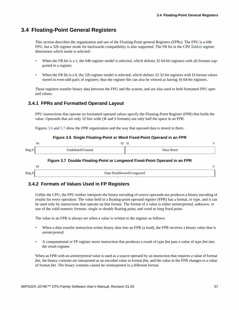
3.4 Floating-Point General Registers
MIPS32® 1074K™ CPU Family Software User’s Manual, Revision 01.03 57
3.4 Floating-Point General Registers
This section describes the organization and use of the Floating-Point general Registers (FPRs). The FPU is a 64bFPU, but a 32b register mode for backwards compatibility is also supported. The FR bit in the CP0 Status registerdetermines which mode is selected:
• When the FR bit is a 1, the 64b register model is selected, which defines 32 64-bit registers with all formats sup-ported in a register.
• When the FR bit is a 0, the 32b register model is selected, which defines 32 32-bit registers with D-format valuesstored in even-odd pairs of registers; thus the register file can also be viewed as having 16 64-bit registers.
These registers transfer binary data between the FPU and the system, and are also used to hold formatted FPU oper-and values.
3.4.1 FPRs and Formatted Operand Layout
FPU instructions that operate on formatted operand values specify the Floating-Point Register (FPR) that holds thevalue. Operands that are only 32 bits wide (W and S formats) use only half the space in an FPR.
Figures 3.6 and 3.7 show the FPR organization and the way that operand data is stored in them.
Figure 3.6 Single Floating-Point or Word Fixed-Point Operand in an FPR
Figure 3.7 Double Floating-Point or Longword Fixed-Point Operand in an FPR
3.4.2 Formats of Values Used in FP Registers
Unlike the CPU, the FPU neither interprets the binary encoding of source operands nor produces a binary encoding ofresults for every operation. The value held in a floating-point operand register (FPR) has a format, or type, and it canbe used only by instructions that operate on that format. The format of a value is either uninterpreted, unknown, orone of the valid numeric formats: single or double floating point, and word or long fixed point.
The value in an FPR is always set when a value is written to the register as follows:
• When a data transfer instruction writes binary data into an FPR (a load), the FPR receives a binary value that isuninterpreted.
• A computational or FP register move instruction that produces a result of type fmt puts a value of type fmt intothe result register.
When an FPR with an uninterpreted value is used as a source operand by an instruction that requires a value of formatfmt, the binary contents are interpreted as an encoded value in format fmt, and the value in the FPR changes to a valueof format fmt. The binary contents cannot be reinterpreted in a different format.
63 32 31 0
Reg 0 Undefined/Unused Data Word
63 0
Reg 0 Data Doubleword/Longword

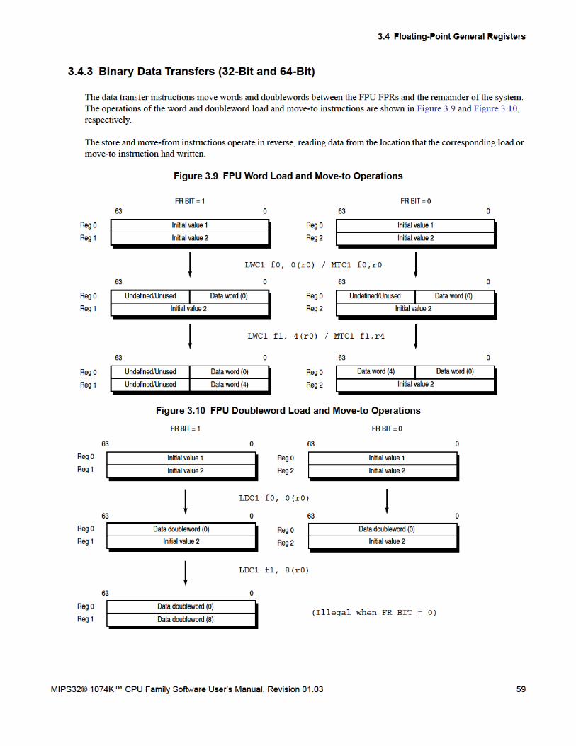

Floating-Point Unit of the 1074Kf™ CPU
60 MIPS32® 1074K™ CPU Family Software User’s Manual, Revision 01.03
3.5 Floating-Point Control Registers
The FPU Control Registers (FCRs) identify and control the FPU. The five FPU control registers are 32 bits wide:FIR, FCCR, FEXR, FENR, FCSR. Three of these registers, FCCR, FEXR, and FENR, select subsets of the float-ing-point Control/Status register, the FCSR. These registers are also denoted Coprocessor 1 (CP1) control registers.
CP1 control registers are summarized in Table 3.4 and are described individually in the following subsections of thischapter. Each register’s description includes the read/write properties and the reset state of each field.
Table 3.5 defines the notation used for the read/write properties of the register bit fields.
Table 3.4 Coprocessor 1 Register Summary
Register Number Register Name Function
0 FIR Floating-Point Implementation register. Contains information that identifiesthe FPU.
25 FCCR Floating-Point Condition Codes register.
26 FEXR Floating-Point Exceptions register.
28 FENR Floating-Point Enables register.
31 FCSR Floating-Point Control and Status register.
Table 3.5 Read/Write Properties
Read/WriteNotation Hardware Interpretation Software Interpretation
R/W All bits in this field are readable and writable by software and potentially by hardware.Hardware updates of this field are visible by software reads. Software updates of this field are visible by hardwarereads.If the reset state of this field is “Undefined,” either software or hardware must initialize the value before the first readreturns a predictable value. This definition should not be confused with the formal definition of UNDEFINED behav-ior.
R This field is either static or is updated only by hardware.If the Reset State of this field is either “0” or “Preset”,hardware initializes this field to zero or to the appropriatestate, respectively, on powerup.If the Reset State of this field is “Undefined”, hardwareupdates this field only under those conditions specified inthe description of the field.
A field to which the value written by software is ignoredby hardware. Software may write any value to this fieldwithout affecting hardware behavior. Software reads ofthis field return the last value updated by hardware.If the Reset State of this field is “Undefined,” softwarereads of this field result in an UNPREDICTABLE valueexcept after a hardware update done under the conditionsspecified in the description of the field.
0 Hardware does not update this field. Hardware can assumea zero value.
The value software writes to this field must be zero. Soft-ware writes of non-zero values to this field might result inUNDEFINED behavior of the hardware. Software reads ofthis field return zero as long as all previous software writesare zero.If the Reset State of this field is “Undefined,” softwaremust write this field with zero before it is guaranteed toread as zero.

3.5 Floating-Point Control Registers
MIPS32® 1074K™ CPU Family Software User’s Manual, Revision 01.03 61
3.5.1 Floating-Point Implementation Register (FIR, CP1 Control Register 0)
The Floating-Point Implementation Register (FIR) is a 32-bit read-only register that contains information identifyingthe capabilities of the FPU, the Floating-Point processor identification, and the revision level of the FPU. Figure 3.11shows the format of the FIR; Table 3.6 describes the FIR bit fields.
Figure 3.11 FIR Format31 25 24 23 22 21 20 19 18 17 16 15 8 7 0
0 FC 0 F64 L W 3D PS D S ProcessorID Revision
Table 3.6 FIR Bit Field Descriptions
Fields
DescriptionRead /Write Reset StateName Bits
FC 24 Indicates that full convert ranges are implemented:• 0: Full convert ranges not implemented• 1: Full convert ranges implementedThis bit is always 1 to indicate that full convert ranges areimplemented. This means that all numbers can be converted toanother type by the FPU (If FS bit in FCSR is not set Unimple-mented Operation exception can still happen on denormal oper-ands though).
R 1
F64 22 Indicates that this is a 64-bit FPU:• 0: Not a 64-bit FPU• 1: A 64-bit FPU.This bit is always 1 to indicate that this is a 64-bit FPU.
R 1
L 21 Indicates that the long fixed point (L) data type and instructionsare implemented:• 0: Long type not implemented• 1: Long implementedThis bit is always 1 to indicate that long fixed point data typesare implemented.
R 1
W 20 Indicates that the word fixed point (W) data type and instruc-tions are implemented:• 0: Word type not implemented• 1: Word implementedThis bit is always 1 to indicate that word fixed point data typesare implemented.
R 1
3D 19 Indicates that the MIPS-3D ASE is implemented:• 0: MIPS-3D not implemented• 1: MIPS-3D implementedThis bit is always 0 to indicate that MIPS-3D is not imple-mented.
R 0
PS 18 Indicates that the paired-single (PS) floating-point data typeand instructions are implemented:• 0: PS floating-point not implemented• 1: PS floating-point implementedThis bit is always 0 to indicate that paired-single floating-pointdata types are not implemented.
R 0

Floating-Point Unit of the 1074Kf™ CPU
62 MIPS32® 1074K™ CPU Family Software User’s Manual, Revision 01.03
3.5.2 Floating-Point Condition Codes Register (FCCR, CP1 Control Register 25)
The Floating-Point Condition Codes Register (FCCR) is an alternative way to read and write the floating-point condi-tion code values that also appear in the FCSR. Unlike the FCSR, all eight FCC bits are contiguous in the FCCR.Figure 3.12 shows the format of the FCCR; Table 3.7 describes the FCCR bit fields.
Figure 3.12 FCCR Format
3.5.3 Floating-Point Exceptions Register (FEXR, CP1 Control Register 26)
The Floating-Point Exceptions Register (FEXR) is an alternative way to read and write the Cause and Flags fields thatalso appear in the FCSR. Figure 3.13 shows the format of the FEXR; Table 3.8 describes the FEXR bit fields.
D 17 Indicates that the double-precision (D) floating-point data typeand instructions are implemented:• 0: D floating-point not implemented• 1: D floating-point implementedThis bit is always 1 to indicate that double-precision floating-point data types are implemented.
R 1
S 16 Indicates that the single-precision (S) floating-point data typeand instructions are implemented:• 0: S floating-point not implemented• 1: S floating-point implementedThis bit is always 1 to indicate that single-precision floating-point data types are implemented.
R 1
Processor ID 15:8 Identifies the floating-point processor. This value matches thecorresponding field of the CP0 PRId register.
R
0x9a
Revision 7:0 Specifies the revision number of the FPU. This field allowssoftware to distinguish between different revisions of the samefloating-point processor type. This value matches the corre-sponding field of the CP0 PRId register.
R Hardwired
0 31:25, 23 These bits must be written as zeros; they return zeros on reads. 0 0
31 8 7 0
0 FCC
Table 3.7 FCCR Bit Field Descriptions
Fields
DescriptionRead /Write Reset StateName Bits
FCC 7:0 Floating-point condition code. Refer to the description of thisfield in Section 3.5.5 “Floating-Point Control and StatusRegister (FCSR, CP1 Control Register 31)”.
R/W Undefined
0 31:8 These bits must be written as zeros; they return zeros on reads. 0 0
Table 3.6 FIR Bit Field Descriptions (Continued)
Fields
DescriptionRead /Write Reset StateName Bits

3.5 Floating-Point Control Registers
MIPS32® 1074K™ CPU Family Software User’s Manual, Revision 01.03 63
Figure 3.13 FEXR Format
3.5.4 Floating-Point Enables Register (FENR, CP1 Control Register 28)
The Floating-Point Enables Register (FENR) is an alternative way to read and write the Enables, FS, and RM fieldsthat also appear in the FCSR. Figure 3.14 shows the format of the FENR; Table 3.9 describes the FENR bit fields.
Figure 3.14 FENR Format
31 30 29 28 27 26 25 24 23 22 21 20 19 18 17 16 15 14 13 12 11 10 9 8 7 6 5 4 3 2 1 0
0 Cause 0 Flags 0
E V Z O U I V Z O U I
Table 3.8 FEXR Bit Field Descriptions
Fields
DescriptionRead /Write Reset StateName Bits
Cause 17:12 Cause bits. Refer to the description of this field in3.5.5 “Floating-Point Control and Status Register (FCSR,CP1 Control Register 31)”.
R/W Undefined
Flags 6:2 Flag bits. Refer to the description of this field in3.5.5 “Floating-Point Control and Status Register (FCSR,CP1 Control Register 31)”.
R/W Undefined
0 31:18, 11:7,1:0
These bits must be written as zeros; they return zeros onreads.
0 0
31 30 29 28 27 26 25 24 23 22 21 20 19 18 17 16 15 14 13 12 11 10 9 8 7 6 5 4 3 2 1 0
0 Enables 0FS
RM
V Z O U I
Table 3.9 FENR Bit Field Descriptions
Fields
DescriptionRead /Write Reset StateName Bits
Enables 11:7 Enable bits. Refer to the description of this field in3.5.5 “Floating-Point Control and Status Register (FCSR,CP1 Control Register 31)”.
R/W Undefined
FS 2 Flush to Zero bit. Refer to the description of this field in3.5.5 “Floating-Point Control and Status Register (FCSR,CP1 Control Register 31)”.
R/W Undefined
RM 1:0 Rounding mode. Refer to the description of this field in3.5.5 “Floating-Point Control and Status Register (FCSR,CP1 Control Register 31)”.
R/W Undefined
0 31:12, 6:3 These bits must be written as zeros; they return zeros onreads.
0 0

Floating-Point Unit of the 1074Kf™ CPU
64 MIPS32® 1074K™ CPU Family Software User’s Manual, Revision 01.03
3.5.5 Floating-Point Control and Status Register (FCSR, CP1 Control Register 31)
The 32-bit Floating-Point Control and Status Register (FCSR) controls the operation of the FPU and shows the fol-lowing status information:
• selects the default rounding mode for FPU arithmetic operations
• selectively enables traps of FPU exception conditions
• controls some denormalized number handling options
• reports any IEEE exceptions that arose during the most recently executed instruction
• reports any IEEE exceptions that cumulatively arose in completed instructions
• indicates the condition code result of FP compare instructions
Access to the FCSR is not privileged; it can be read or written by any program that has access to the FPU (via thecoprocessor enables in the Status register). Figure 3.15 shows the format of the FCSR; Table 3.10 describes theFCSR bit fields.
Figure 3.15 FCSR Format31 30 29 28 27 26 25 24 23 22 21 20 19 18 17 16 15 14 13 12 11 10 9 8 7 6 5 4 3 2 1 0
FCCFS
FCC
FO
FN
0 Cause Enables Flags RM
7 6 5 4 3 2 1 0 E V Z O U I V Z O U I V Z O U I
Table 3.10 FCSR Bit Field Descriptions
Fields
DescriptionRead /Write Reset StateName Bit
FCC 31:25, 23 Floating-point condition codes. These bits record theresult of floating-point compares and are tested for float-ing-point conditional branches and conditional moves.The FCC bit to use is specified in the compare, branch, orconditional move instruction. For backward compatibilitywith previous MIPS ISAs, the FCC bits are separated intotwo non-contiguous fields.
R/W Undefined
FS 24 Flush to Zero (FS). Refer to 3.5.6 “Operation of the FS/FO/FN Bits” for more details on this bit.
R/W Undefined
FO 22 Flush Override (FO). Refer to Section 3.5.6, "Operation ofthe FS/FO/FN Bits" for more details on this bit.
R/W Undefined
FN 21 Flush to Nearest (FN). Refer to Section 3.5.6, "Operationof the FS/FO/FN Bits" for more details on this bit.
R/W Undefined

3.5 Floating-Point Control Registers
MIPS32® 1074K™ CPU Family Software User’s Manual, Revision 01.03 65
Cause 17:12 Cause bits. These bits indicate the exception conditionsthat arise during execution of an FPU arithmetic instruc-tion. A bit is set to 1 when the corresponding exceptioncondition arises during the execution of an instruction;otherwise, it is cleared to 0. By reading the registers, theexception condition caused by the preceding FPU arith-metic instruction can be determined.Refer to Table 3.11 for the meaning of each cause bit.
R/W Undefined
Enables 11:7 Enable bits. These bits control whether or not a trap istaken when an IEEE exception condition occurs for any ofthe five conditions. The trap occurs when both an enablebit and its corresponding cause bit are set either during anFPU arithmetic operation or by moving a value to theFCSR or one of its alternative representations. Note thatCause bit E (CauseE) has no corresponding enable bit; theMIPS architecture defines non-IEEE UnimplementedOperation exceptions as always enabled.Refer to Table 3.11 for the meaning of each enable bit.
R/W Undefined
Flags 6:2 Flag bits. This field shows any exception conditions thathave occurred for completed instructions since the flagwas last reset by software.When an FPU arithmetic operation raises an IEEE excep-tion condition that does not result in a Floating-PointException (the enable bit was off), the correspondingbit(s) in the Flags field are set, while the others remainunchanged. Arithmetic operations that result in a Floating-Point Exception (the enable bit was on) do not update theFlags field.Hardware never resets this field; software must explicitlyreset this field.Refer to Table 3.11 for the meaning of each flag bit.
R/W Undefined
RM 1:0 Rounding mode. This field indicates the rounding modeused for most floating-point operations (some operationsuse a specific rounding mode).Refer to Table 3.12 for the encoding of this field.
R/W Undefined
0 20:18 These bits must be written as zeros; they return zeros onreads.
0 0
Table 3.11 Cause, Enables, and Flags Definitions
Bit Name Bit Meaning
E Unimplemented Operation (this bit exists only in the Cause field).
V Invalid Operations
Z Divide by Zero
O Overflow
U Underflow
Table 3.10 FCSR Bit Field Descriptions (Continued)
Fields
DescriptionRead /Write Reset StateName Bit

Floating-Point Unit of the 1074Kf™ CPU
66 MIPS32® 1074K™ CPU Family Software User’s Manual, Revision 01.03
3.5.6 Operation of the FS/FO/FN Bits
The FS, FO, and FN bits in the CP1 FCSR register control handling of denormalized operands and tiny results (i.e.
nonzero result between ±2E_min), whereby the FPU can handle these cases right away instead of relying on the muchslower software handler. The trade-off is a loss of IEEE compliance and accuracy (except for use of the FO bit),because a minimal normalized or zero result is provided by the FPU instead of the more accurate denormalized resultthat a software handler would give. The benefit is a significantly improved performance and precision.
Use of the FS, FO, and FN bits affects handling of denormalized floating-point numbers and tiny results for theinstructions listed below:
Instructions not listed above do not cause Unimplemented Operation exceptions on denormalized numbers in oper-ands or results.
Figure 3.16 depicts how the FS, FO, and FN bits control handling of denormalized numbers. For instructions that arenot multiply or add types (such as DIV), only the FS and FN bits apply.
I Inexact
Table 3.12 Rounding Mode Definitions
RM Field Encoding Meaning
0 RN - Round to NearestRounds the result to the nearest representable value. When two representablevalues are equally near, the result is rounded to the value whose least-signifi-cant bit is zero (even).
1 RZ - Round Toward ZeroRounds the result to the value closest to but not greater in magnitude than theresult.
2 RP - Round Towards Plus InfinityRounds the result to the value closest to but not less than the result.
3 RM - Round Towards Minus InfinityRounds the result to the value closest to but not greater than the result.
Table 3.13 Handling Denormalized Floating-point Numbers
FS and FN bit: ADD, CEIL, CVT, DIV, FLOOR, MADD, MSUB, MUL, NMADD, NMSUB, RECIP, ROUND,
RSQRT, SQRT, TRUNC, SUB, ABS, C.cond, and NEG1
1. For ABS, C.cond, and NEG, denormal input operands or tiny results doe not result in Unimplemented exceptionswhen FS = 0. Flushing to zero nonetheless is implemented when FS = 1 such that these operations return the sameresult as an equivalent sequence of arithmetic FPU operations.
FO bit: MADD, MSUB, NMADD, and NMSUB
Table 3.11 Cause, Enables, and Flags Definitions (Continued)
Bit Name Bit Meaning

3.5 Floating-Point Control Registers
MIPS32® 1074K™ CPU Family Software User’s Manual, Revision 01.03 67
Figure 3.16 FS/FO/FN Bits Influence on Multiply and Addition Results
3.5.6.1 Flush To Zero Bit
When the Flush To Zero (FS) bit is set, denormal input operands are flushed to zero. Tiny results are flushed to eitherzero or the applied format’s smallest normalized number (MinNorm) depending on the rounding mode settings. Table3.14 lists the flushing behavior for tiny results..
The flushing of results is based on an intermediate result computed by rounding the mantissa using an unboundedexponent range; that is, tiny numbers are not normalized into the supported exponent range by shifting in leadingzeros prior to rounding.
Handling of denormalized operand values and tiny results depends on the FS bit setting as shown in Table 3.15.
3.5.6.2 Flush Override Bit
When the Flush Override (FO) bit is set, a tiny intermediate result of any multiply-add type instruction is not flushedaccording to the FS bit. The intermediate result is maintained in an internal normalized format to improve accuracy.FO only applies to the intermediate result of a multiply-add type instruction.
Handling of tiny intermediate results depends on the FO and FS bits as shown in Table 3.16.
Table 3.14 Zero Flushing for Tiny Results
Rounding Mode Negative Tiny Result Positive Tiny Result
RN (RM=0) -0 +0
RZ(RM=1) -0 +0
RP (RM=2) -0 +MinNorm
RM (RM=3) -MinNorm +0
Table 3.15 Handling of Denormalized Operand Values and Tiny Results Based on FS Bit Setting
FS Bit Handling of Denormalized Operand Values
0 An Unimplemented Operation exception is taken.
1 Instead of causing an Unimplemented Operation exception, operands are flushed to zero, and tinyresults are forced to zero or MinNorm.
Table 3.16 Handling of Tiny Intermediate Result Based on the FO and FS Bit Settings
FO Bit FS Bit Handling of Tiny Result Values
0 0 An Unimplemented Operation exception is taken.
Operand valuesFS applies
AdditionMultiply
Intermediate Multiply-Add resultFS/FO applies
Final resultFS/FN applies

Floating-Point Unit of the 1074Kf™ CPU
68 MIPS32® 1074K™ CPU Family Software User’s Manual, Revision 01.03
3.5.6.3 Flush to Nearest
When the Flush to Nearest (FN) bit is set and the rounding mode is Round to Nearest (RN), a tiny final result isflushed to zero or MinNorm. If a tiny number is strictly below MinNorm/2, the result is flushed to zero; otherwise, itis flushed to MinNorm (see Figure 3.17). The flushed result has the same sign as the result prior to flushing. Note thatthe FN bit takes precedence over the FS bit.
Figure 3.17 Flushing to Nearest when Rounding Mode is Round to Nearest
For all rounding modes other than Round to Nearest (RN), setting the FN bit causes final results to be flushed to zeroor MinNorm as if the FS bit was set.
Handling of tiny final results depends on the FN and FS bits as shown in Table 3.17.
0 1 The intermediate result is forced to the value that would have been delivered for anuntrapped underflow (see Table 3.34) instead of causing an Unimplemented Opera-tion exception.
1 Don’t care The intermediate result is kept in an internal format, which can be perceived as hav-ing the usual mantissa precision but with unlimited exponent precision and withoutforcing to a specific value or taking an exception.
Table 3.17 Handling of Tiny Final Result Based on FN and FS Bit Settings
FN Bit FS Bit Handling of Tiny Result Values
0 0 An Unimplemented Operation exception is taken.
0 1 Final result is forced to the value that would have been delivered for an untrappedunderflow (see Table 3.34) rather than causing an Unimplemented Operationexception.
1 Don’t care Final result is rounded to either zero or 2E_min (MinNorm), whichever is closestwhen in Round to Nearest (RN) rounding mode. For other rounding modes, a finalresult is given as if FS was set to 1.
Table 3.16 Handling of Tiny Intermediate Result Based on the FO and FS Bit Settings (Continued)
FO Bit FS Bit Handling of Tiny Result Values
MinNorm/2-MinNorm/2
-MinNorm MinNorm0

3.5 Floating-Point Control Registers
MIPS32® 1074K™ CPU Family Software User’s Manual, Revision 01.03 69
3.5.6.4 Recommended FS/FO/FN Settings
Table 3.18 summarizes the recommended FS/FO/FN settings.
3.5.7 FCSR Cause Bit Update Flow
3.5.7.1 Exceptions Triggered by CTC1
Regardless of the targeted control register, the CTC1 instruction causes the Enables and Cause fields of the FCSR tobe inspected in order to determine if an exception is to be thrown.
3.5.7.2 Generic Flow
Computations are performed in two steps:
1. Compute rounded mantissa with unbound exponent range.
2. Flush to default result if the result from Step #1 above is overflow or tiny (no flushing happens on denorms forinstructions supporting denorm results, such as MOV).
The Cause field is updated after each of these two steps. Any enabled exceptions detected in these two steps cause atrap, and no further updates to the Cause field are done by subsequent steps.
Step #1 can set cause bits I, U, O, Z, V, and E. E has priority over V; V has priority over Z; and Z has priority over Uand O. Thus when E, V, or Z is set in Step #1, no other cause bits can be set. However, note that I and V both can beset if a denormal operand was flushed (FS = 1). I, U, and O can be set alone or in pairs (IU or IO). U and O never canbe set simultaneously in Step #1. U and O are set if the computed unbounded exponent is outside the exponent rangesupported by the normalized IEEE format.
Step #2 can set I if a default result is generated.
3.5.7.3 Multiply-Add Flow
For multiply-add type instructions, the computation is extended with two more steps:
1. Compute rounded mantissa with unbound exponent range for the multiply.
2. Flush to default result if the result from Step #1 is overflow or tiny (no flushing happens on tiny results ifFO = 1).
3. Compute rounded mantissa with unbounded exponent range for the add.
Table 3.18 Recommended FS/FO/FN Settings
FS Bit FO Bit FN Bit Remarks
0 0 0 IEEE-compliant mode. Low performance on denormal operands and tinyresults.
1 0 0 Regular embedded applications. High performance on denormal operandsand tiny results.
1 1 1 Highest accuracy and performance configuration.1
1. Note that in this mode, MADD might return a different result other than the equivalent MUL and ADD opera-tion sequence.
Floating-Point Unit of the 1074Kf™ CPU
70 MIPS32® 1074K™ CPU Family Software User’s Manual, Revision 01.03
4. Flush to default result if the result from Step #3 is overflow or tiny.
The Cause field is updated after each of these four steps. Any enabled exceptions detected in these four steps cause atrap, and no further updates to the Cause field are done by subsequent steps.
Step #1 and Step #3 can set a cause bit as described for Step #1 in 3.5.7.2 “Generic Flow”.
Step #2 and Step #4 can set I if a default result is generated.
Although U and O can never both be set in Step #1 or Step #3, both U and O might be set after the multiply-add hasexecuted in Step #3 because U might be set in Step #1 and O might be set in Step #3.
3.5.7.4 Cause Update Flow for Input Operands
Denormal input operands to Step #1 or Step #3 always set Cause bit I when FS = 1. For example, SNaN+DeNorm setI (and V) provided that Step #3 was reached (in case of a multiply-add type instruction).
Conditions directly related to the input operand (for example, I/E set due to DeNorm, V set due to SNaN and QNaNpropagation) are detected in the step where the operand is logically used. For example, for multiply-add type instruc-tions, exceptional conditions caused by the input operand fr are detected in Step #3.
3.5.7.5 Cause Update Flow for Unimplemented Operations
Note that Cause bit E is special; it clears any Cause updates done in previous steps. For example, if Step #3 caused Eto be set, any I, U, or O Cause update done in Step #1 or Step #2 is cleared. Only E is set in the Cause field when anUnimplemented Operation trap is taken.
3.6 Instruction Overview
The functional groups into which the FPU instructions are divided are described in the following subsections:
• Section 3.6.1 “Data Transfer Instructions”
• Section 3.6.2 “Arithmetic Instructions”
• Section 3.6.3 “Conversion Instructions”
• Section 3.6.4 “Formatted Operand-Value Move Instructions”
• Section 3.6.5 “Conditional Branch Instructions”
• Section 3.6.6 “Miscellaneous Instructions”
The instructions are described in detail in Chapter 13, “1074K™ CPU Instructions”, including descriptions of sup-ported formats (fmt).
3.6.1 Data Transfer Instructions
The FPU has two separate register sets: coprocessor general registers (FPRs) and coprocessor control registers(FCRs). The FPU has a load/store architecture; all computations are done on data held in coprocessor general regis-ters. The control registers are used to control FPU operation. Data is transferred between registers and the rest of the

3.6 Instruction Overview
MIPS32® 1074K™ CPU Family Software User’s Manual, Revision 01.03 71
system with dedicated load, store, and move instructions. The transferred data is treated as unformatted binary data;no format conversions are performed, and therefore no IEEE floating-point exceptions can occur.
Table 3.19 lists the supported transfer operations.
3.6.1.1 Data Alignment in Loads, Stores, and Moves
All coprocessor loads and stores operate on naturally aligned data items. An attempt to load or store to an address thatis not naturally aligned for the data item causes an Address Error exception. Regardless of byte ordering (the endian-ness), the address of a word or doubleword is the smallest byte address in the object. For a big-endian machine, this isthe most-significant byte; for a little-endian machine, this is the least-significant byte.
3.6.1.2 Addressing Used in Data Transfer Instructions
The FPU has loads and stores using the same register+offset addressing as that used by the CPU. Moreover, for theFPU only, there are load and store instructions using register+register addressing.
Tables 3.20 through 3.22 list the FPU data transfer instructions.
Table 3.19 FPU Data Transfer Instructions
Transfer Direction Data Transferred
FPU general register ↔ Memory Word/doubleword load/store
FPU general register ↔ CPU general register Word move
FPU control register ↔ CPU general register Word move
Table 3.20 FPU Loads and Stores Using Register+Offset Address Mode
Mnemonic Instruction
LDC1 Load Doubleword to Floating Point
LWC1 Load Word to Floating Point
SDC1 Store Doubleword to Floating Point
SWC1 Store Word to Floating Point
Table 3.21 FPU Loads and Stores Using Register+Register Address Mode
Mnemonic Instruction
LDXC1 Load Doubleword Indexed to Floating Point
LUXC1 Load Doubleword Indexed Unaligned to Floating Point
LWXC1 Load Word Indexed to Floating Point
SDXC1 Store Doubleword Indexed to Floating Point
SUXC1 Store Doubleword Indexed Unaligned to Floating Point
SWXC1 Store Word Indexed to Floating Point
Table 3.22 FPU Move To and From Instructions
Mnemonic Instruction
CFC1 Move Control Word From Floating Point
CTC1 Move Control Word To Floating Point

Floating-Point Unit of the 1074Kf™ CPU
72 MIPS32® 1074K™ CPU Family Software User’s Manual, Revision 01.03
3.6.2 Arithmetic Instructions
Arithmetic instructions operate on formatted data values. The results of most floating-point arithmetic operationsmeet IEEE Standard 754 for accuracy—a result is identical to an infinite-precision result that has been rounded to thespecified format using the current rounding mode. The rounded result differs from the exact result by less than oneUnit in the Least-significant Place (ULP).
In general, the arithmetic instructions take an Umimplemented Operation exception for denormalized numbers,except for the ABS, C, and NEG instructions, which can handle denormalized numbers. The FS, FO, and FN bits inthe CP1 FCSR register can override this behavior as described in Section 3.5.6, "Operation of the FS/FO/FN Bits".
Table 3.23 lists the FPU IEEE compliant arithmetic operations.
The two low latency operations, Reciprocal Approximation (RECIP) and Reciprocal Square Root Approximation(RSQRT), might be less accurate than the IEEE specification:
• The result of RECIP differs from the exact reciprocal by no more than one ULP.
• The result of RSQRT differs from the exact reciprocal square root by no more than two ULPs.
Table 3.24 lists the FPU-approximate arithmetic operations.
Four compound-operation instructions perform variations of multiply-accumulate operations; that is, multiply twooperands, accumulate the result to a third operand, and produce a result. These instructions are listed in Table 3.25.The product is rounded according to the current rounding mode prior to the accumulation. This model meets the IEEE
MFC1 Move Word From Floating Point
MTC1 Move Word To Floating Point
Table 3.23 FPU IEEE Arithmetic Operations
Mnemonic Instruction
ABS.fmt Floating-Point Absolute Value
ADD.fmt Floating-Point Add
C.cond.fmt Floating-Point Compare
DIVfmt Floating-Point Divide
MUL fmt Floating-Point Multiply
NEG fmt Floating-Point Negate
SQRT fmt Floating-Point Square Root
SUB.fmt Floating-Point Subtract
Table 3.24 FPU-Approximate Arithmetic Operations
Mnemonic Instruction
RECIP fmt Floating-Point Reciprocal Approximation
RSQRT fmt Floating-Point Reciprocal Square Root Approximation
Table 3.22 FPU Move To and From Instructions (Continued)
Mnemonic Instruction
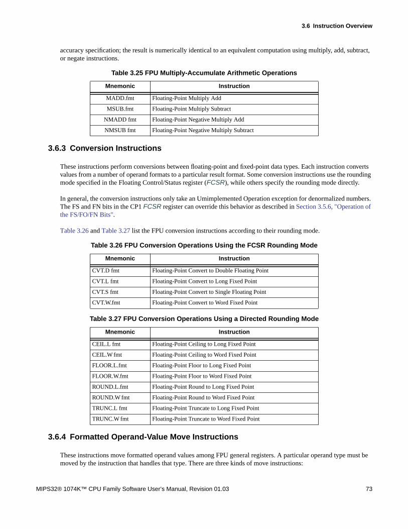
3.6 Instruction Overview
MIPS32® 1074K™ CPU Family Software User’s Manual, Revision 01.03 73
accuracy specification; the result is numerically identical to an equivalent computation using multiply, add, subtract,or negate instructions.
3.6.3 Conversion Instructions
These instructions perform conversions between floating-point and fixed-point data types. Each instruction convertsvalues from a number of operand formats to a particular result format. Some conversion instructions use the roundingmode specified in the Floating Control/Status register (FCSR), while others specify the rounding mode directly.
In general, the conversion instructions only take an Umimplemented Operation exception for denormalized numbers.The FS and FN bits in the CP1 FCSR register can override this behavior as described in Section 3.5.6, "Operation ofthe FS/FO/FN Bits".
Table 3.26 and Table 3.27 list the FPU conversion instructions according to their rounding mode.
3.6.4 Formatted Operand-Value Move Instructions
These instructions move formatted operand values among FPU general registers. A particular operand type must bemoved by the instruction that handles that type. There are three kinds of move instructions:
Table 3.25 FPU Multiply-Accumulate Arithmetic Operations
Mnemonic Instruction
MADD.fmt Floating-Point Multiply Add
MSUB.fmt Floating-Point Multiply Subtract
NMADD fmt Floating-Point Negative Multiply Add
NMSUB fmt Floating-Point Negative Multiply Subtract
Table 3.26 FPU Conversion Operations Using the FCSR Rounding Mode
Mnemonic Instruction
CVT.D fmt Floating-Point Convert to Double Floating Point
CVT.L fmt Floating-Point Convert to Long Fixed Point
CVT.S fmt Floating-Point Convert to Single Floating Point
CVT.W.fmt Floating-Point Convert to Word Fixed Point
Table 3.27 FPU Conversion Operations Using a Directed Rounding Mode
Mnemonic Instruction
CEIL.L fmt Floating-Point Ceiling to Long Fixed Point
CEIL.W fmt Floating-Point Ceiling to Word Fixed Point
FLOOR.L.fmt Floating-Point Floor to Long Fixed Point
FLOOR.W.fmt Floating-Point Floor to Word Fixed Point
ROUND.L.fmt Floating-Point Round to Long Fixed Point
ROUND.W fmt Floating-Point Round to Word Fixed Point
TRUNC.L fmt Floating-Point Truncate to Long Fixed Point
TRUNC.W fmt Floating-Point Truncate to Word Fixed Point

Floating-Point Unit of the 1074Kf™ CPU
74 MIPS32® 1074K™ CPU Family Software User’s Manual, Revision 01.03
• Unconditional move
• Conditional move that tests an FPU true/false condition code
• Conditional move that tests a CPU general-purpose register against zero
Conditional move instructions operate in a way that might be unexpected. They always force the value in the destina-tion register to become a value of the format specified in the instruction. If the destination register does not contain anoperand of the specified format before the conditional move is executed, the contents become undefined. (For moreinformation, see the individual descriptions of the conditional move instructions in the MIPS32 Architecture Refer-ence Manual, Volume II.)
Table 3.28 through Table 3.30 list the formatted operand-value move instructions.
3.6.5 Conditional Branch Instructions
The FPU has PC-relative conditional branch instructions that test condition codes set by FPU compare instructions(C.cond fmt).
All branches have an architectural delay of one instruction. When a branch is taken, the instruction immediately fol-lowing the branch instruction is said to be in the branch delay slot; it is executed before the branch to the targetinstruction takes place. Conditional branches come in two versions, depending upon how they handle an instruction inthe delay slot when the branch is not taken and execution falls through:
• Branch instructions execute the instruction in the delay slot.
• Branch likely instructions do not execute the instruction in the delay slot if the branch is not taken (they are saidto nullify the instruction in the delay slot).
Although the Branch Likely instructions are included, software is strongly encouraged to avoid the use ofthe Branch Likely instructions, as they will be removed from a future revision of the MIPS Architecture.
Table 3.28 FPU Formatted Operand Move Instruction
Mnemonic Instruction
MOV.fmt Floating-Point Move
Table 3.29 FPU Conditional Move on True/False Instructions
Mnemonic Instruction
MOVF fmt Floating-Point Move Conditional on FP False
MOVT.fmt Floating-Point Move Conditional on FP True
Table 3.30 FPU Conditional Move on Zero/Non-Zero Instructions
Mnemonic Instruction
MOVN fmt Floating-Point Move Conditional on Nonzero
MOVZ fmt Floating-Point Move Conditional on Zero
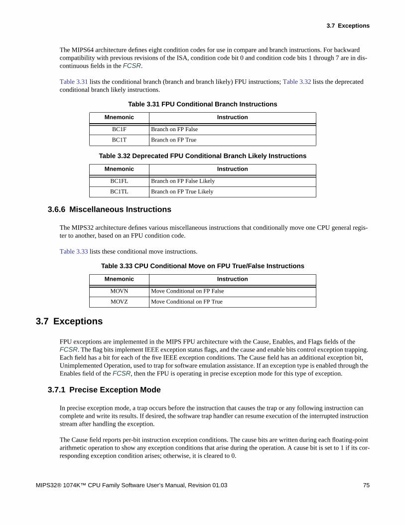
3.7 Exceptions
MIPS32® 1074K™ CPU Family Software User’s Manual, Revision 01.03 75
The MIPS64 architecture defines eight condition codes for use in compare and branch instructions. For backwardcompatibility with previous revisions of the ISA, condition code bit 0 and condition code bits 1 through 7 are in dis-continuous fields in the FCSR.
Table 3.31 lists the conditional branch (branch and branch likely) FPU instructions; Table 3.32 lists the deprecatedconditional branch likely instructions.
3.6.6 Miscellaneous Instructions
The MIPS32 architecture defines various miscellaneous instructions that conditionally move one CPU general regis-ter to another, based on an FPU condition code.
Table 3.33 lists these conditional move instructions.
3.7 Exceptions
FPU exceptions are implemented in the MIPS FPU architecture with the Cause, Enables, and Flags fields of theFCSR. The flag bits implement IEEE exception status flags, and the cause and enable bits control exception trapping.Each field has a bit for each of the five IEEE exception conditions. The Cause field has an additional exception bit,Unimplemented Operation, used to trap for software emulation assistance. If an exception type is enabled through theEnables field of the FCSR, then the FPU is operating in precise exception mode for this type of exception.
3.7.1 Precise Exception Mode
In precise exception mode, a trap occurs before the instruction that causes the trap or any following instruction cancomplete and write its results. If desired, the software trap handler can resume execution of the interrupted instructionstream after handling the exception.
The Cause field reports per-bit instruction exception conditions. The cause bits are written during each floating-pointarithmetic operation to show any exception conditions that arise during the operation. A cause bit is set to 1 if its cor-responding exception condition arises; otherwise, it is cleared to 0.
Table 3.31 FPU Conditional Branch Instructions
Mnemonic Instruction
BC1F Branch on FP False
BC1T Branch on FP True
Table 3.32 Deprecated FPU Conditional Branch Likely Instructions
Mnemonic Instruction
BC1FL Branch on FP False Likely
BC1TL Branch on FP True Likely
Table 3.33 CPU Conditional Move on FPU True/False Instructions
Mnemonic Instruction
MOVN Move Conditional on FP False
MOVZ Move Conditional on FP True

Floating-Point Unit of the 1074Kf™ CPU
76 MIPS32® 1074K™ CPU Family Software User’s Manual, Revision 01.03
A floating-point trap is generated any time both a cause bit and its corresponding enable bit are set. This case occurseither during the execution of a floating-point operation or when moving a value into the FCSR. There is no enablebit for Unimplemented Operations; this exception always generates a trap.
In a trap handler, exception conditions that arise during any trapped floating-point operations are reported in theCause field. Before returning from a floating-point interrupt or exception, or before setting cause bits with a move tothe FCSR, software first must clear the enabled cause bits by executing a move to the FCSR to prevent the trap frombeing erroneously retaken.
If a floating-point operation sets only non-enabled cause bits, no trap occurs and the default result defined by IEEEStandard 754 is stored (see Table 3.34). When a floating-point operation does not trap, the program can monitor theexception conditions by reading the Cause field.
The Flags field is a cumulative report of IEEE exception conditions that arise as instructions complete; instructionsthat trap do not update the flag bits. The flag bits are set to 1 if the corresponding IEEE exception is raised, otherwisethe bits are unchanged. There is no flag bit for the MIPS Unimplemented Operation exception. The flag bits are nevercleared as a side effect of floating-point operations, but they can be set or cleared by moving a new value into theFCSR.
3.7.2 Exception Conditions
The subsections below describe the following five exception conditions defined by IEEE Standard 754:
• Section 3.7.2.1 “Invalid Operation Exception”
• Section 3.7.2.2 “Division By Zero Exception”
• Section 3.7.2.3 “Underflow Exception”
• Section 3.7.2.4 “Overflow Exception”
• Section 3.7.2.5 “Inexact Exception”
3.7.2.6 “Unimplemented Operation Exception” also describes a MIPS-specific exception condition, UnimplementedOperation Exception, that is used to signal a need for software emulation of an instruction. Normally an IEEE arith-metic operation can cause only one exception condition; the only case in which two exceptions can occur at the sametime are Inexact With Overflow and Inexact With Underflow.
At the program’s direction, an IEEE exception condition can either cause a trap or not cause a trap. IEEE Standard754 specifies the result to be delivered in case no trap is taken. The FPU supplies these results whenever the exceptioncondition does not result in a trap. The default action taken depends on the type of exception condition and, in thecase of the Overflow and Underflow, the current rounding mode. Table 3.34 summarizes the default results.
Table 3.34 Result for Exceptions Not Trapped
Bit Description Default Action
V Invalid Operation Supplies a quiet NaN.
Z Divide by zero Supplies a properly signed infinity.

3.7 Exceptions
MIPS32® 1074K™ CPU Family Software User’s Manual, Revision 01.03 77
3.7.2.1 Invalid Operation Exception
An Invalid Operation exception is signaled when one or both of the operands are invalid for the operation to be per-formed. When the exception condition occurs without a precise trap, the result is a quiet NaN.
The following operations are invalid:
• One or both operands are a signaling NaN (except for the non-arithmetic MOVfmt, MOVT fmt, MOVF.fmt,MOVN.fmt, and MOVZ.fmt instructions).
• Addition or subtraction: magnitude subtraction of infinities, such as (+∞) + (−∞) or (−∞) - (−∞).
• Multiplication: 0 × ∞, with any signs.
• Division: 0/0 or ∞/∞, with any signs.
• Square root: An operand of less than 0 (-0 is a valid operand value).
• Conversion of a floating-point number to a fixed-point format when either an overflow or an operand value ofinfinity or NaN precludes a faithful representation in that format.
• Some comparison operations in which one or both of the operands is a QNaN value.
3.7.2.2 Division By Zero Exception
The divide operation signals a Division By Zero exception if the divisor is zero and the dividend is a finite nonzeronumber. When no precise trap occurs, the result is a correctly signed infinity. Divisions (0/0 and ∞/0) do not cause theDivision By Zero exception. The result of (0/0) is an Invalid Operation exception. The result of (∞/0) is a correctlysigned infinity.
U Underflow Depends on the rounding mode as shown below:• 0 (RN) and 1 (RZ): Supplies a zero with the sign of the exact result.
• 2 (RP): For positive underflow values, supplies 2E_min (MinNorm). For negativeunderflow values, supplies a positive zero.
• 3 (RM): For positive underflow values, supplies a negative zero. For negative under-
flow values, supplies a negative 2E_min (MinNorm).Note that this behavior is only valid if the FCSR FN bit is cleared.
I Inexact Supplies a rounded result. If caused by an overflow without the overflow trap enabled,supplies the overflowed result. If caused by an underflow without the underflow trapenabled, supplies the underflowed result.
O Overflow Depends on the rounding mode, as shown below:• 0 (RN): Supplies an infinity with the sign of the exact result.• 1 (RZ): Supplies the format’s largest finite number with the sign of the exact result.• 2 (RP): For positive overflow values, supplies positive infinity. For negative overflow
values, supplies the format’s most negative finite number.• 3 (RM): For positive overflow values, supplies the format’s largest finite number. For
negative overflow values, supplies minus infinity.
Table 3.34 Result for Exceptions Not Trapped (Continued)
Bit Description Default Action
Floating-Point Unit of the 1074Kf™ CPU
78 MIPS32® 1074K™ CPU Family Software User’s Manual, Revision 01.03
3.7.2.3 Underflow Exception
Two related events contribute to underflow:
• Tininess: The creation of a tiny, nonzero result between ±2E_min which, because it is tiny, might cause some otherexception later such as overflow on division. IEEE Standard 754 allows choices in detecting tininess events. TheMIPS architecture specifies that tininess be detected after rounding, when a nonzero result computed as though
the exponent range were unbounded would lie strictly between ±2E_min.
• Loss of accuracy: The extraordinary loss of accuracy occurs during the approximation of such tiny numbers bydenormalized numbers. IEEE Standard 754 allows choices in detecting loss of accuracy events. The MIPS archi-tecture specifies that loss of accuracy be detected as inexact result, when the delivered result differs from whatwould have been computed if both the exponent range and precision were unbounded.
The way that an underflow is signaled depends on whether or not underflow traps are enabled:
• When an underflow trap is not enabled, underflow is signaled only when both tininess and loss of accuracy have
been detected. The delivered result might be zero, denormalized, or 2E_min.
• When an underflow trap is enabled (through the FCSR Enables field), underflow is signaled when tininess isdetected regardless of loss of accuracy.
3.7.2.4 Overflow Exception
An Overflow exception is signaled when the magnitude of a rounded floating-point result (if the exponent range isunbounded) is larger than the destination format’s largest finite number.
When no precise trap occurs, the result is determined by the rounding mode and the sign of the intermediate result.
3.7.2.5 Inexact Exception
An Inexact exception is signaled when one of the following occurs:
• The rounded result of an operation is not exact.
• The rounded result of an operation overflows without an overflow trap.
• When a denormal operand is flushed to zero.
3.7.2.6 Unimplemented Operation Exception
The Unimplemented Operation exception is a MIPS-defined exception that provides software emulation support. Thisexception is not IEEE-compliant.
The MIPS architecture is designed so that a combination of hardware and software can implement the architecture.Operations not fully supported in hardware cause an Unimplemented Operation exception, allowing software to per-form the operation.
There is no enable bit for this condition; it always causes a trap (but the condition is effectively masked for all opera-tions when FS=1). After the appropriate emulation or other operation is done in a software exception handler, theoriginal instruction stream can be continued.
An Unimplemented Operation exception is taken in the following situations:

3.8 Pipeline and Performance
MIPS32® 1074K™ CPU Family Software User’s Manual, Revision 01.03 79
• when denormalized operands or tiny results are encountered for instructions not supporting denormal numbersand where such are not handed by the FS/FO/FN bits.
3.8 Pipeline and Performance
This section describes the structure and operation of the FPU pipeline.
3.8.1 Pipeline Overview
The FPU has a seven stage pipeline to which the integer pipeline dispatches instructions. The FPU supports limiteddual-issue. It can accept one “to/from” instruction and one arithmetic instruction every cycle. A “to/from” instructionis a data transfer instruction and covers the following instructions: MFC1, MFHC1, MTC1, MTHC1, CFC1, CTC1,LWC1, LWXC1, LUXC1, LDC1, LDXC1, SWC1, SWXC1, SDC1 and SDXC1. The arithmetic group refers to allother floating point instructions.
The FPU pipeline runs in parallel with the 1074K integer pipeline. The FPU can be built to run at different frequen-cies compared to the integer core. The supported ratios of integer core clock to FPU clk are: 2:1, 3:2 and 1:1.
The FPU pipe is optimized for single-precision instructions, such that the basic multiply, ADD/SUB, and MADD/MSUB instructions can be performed with single-cycle throughput and low latency. Executing double-precision mul-tiply and MADD/MSUB instructions requires a second pass through the M1 stage to generate all 64 bits of the prod-uct. Executing long latency instructions, such as DIV and RSQRT, extends the M1 stage. Figure 3.18 shows the FPUpipeline.
Figure 3.18 FPU Pipeline
3.8.1.1 DR Stage - Dispatch Rename
The DR stage is described in detail in Chapter 2, “Pipeline of the 1074K™ CPU”. This stage is common to both theinteger and floating point pipeline. The two pipelines fork off separately after this stage.
3.8.1.2 C1 - Coprocessor Interface Unit Stage 1
In this stage, the Coprocessor Interface Unit (CIU) receives two instructions from the IDU. It does some preliminarydecoding and determines if there is space available in its internal queues for the received instructions.
1074K integerpipeline
FPU instruction in general
FPU double multiplication (for example, MUL, MADD)
FPU long instructions (for example, DIV, RSQRT)
Dispatch
FR M1 M2 A1 A2 FP
FR M1 M1 M2 A1 A2
FW
FWFP
FR M1 M1 M2 A1 A2 FWFP
SecondPass
Multiple cycles
DR C1 C2 CR CI
Floating-Point Unit of the 1074Kf™ CPU
80 MIPS32® 1074K™ CPU Family Software User’s Manual, Revision 01.03
3.8.1.3 CR Stage - Coprocessor Interface Unit Queue Read
The CIU internal instruction queues are read in this stage and up to two instructions are selected for dispatch to theFPU.
3.8.1.4 CI Stage - Coprocessor 1 Interface
This pipeline stage represents the interface stage, where instructions are sent to the FPU
3.8.1.5 FR Stage - Decode, Register Read, and Unpack
This pipeline is the second interface stage, where the instruction start is sent to the FPU.
The FR stage also has the following additional functionality:
• The dispatched instruction is decoded for register accesses.
• Data is read from the register file.
• The operands are unpacked into an internal format.
3.8.1.6 M1 Stage - Multiply Tree
The M1 stage has the following functionality:
• A single-cycle multiply array is provided for single-precision data format multiplication, and two cycles are pro-vided for double-precision data format multiplication.
• The long instructions, such as divide and square root, iterate for several cycles in this stage.
• Sum of exponents is calculated.
• If an exception can be predicted, then it is sent out in this pipeline stage.
3.8.1.7 M2 Stage - Multiply Complete
The M2 stage has the following functionality:
• Multiplication is complete when the carry-save encoded product is compressed into binary.
• Rounding is performed.
• Exponent difference for addition path is calculated.
3.8.1.8 A1 Stage - Addition First Step
This stage performs the first step of the addition.
3.8.1.9 A2 Stage - Addition Second and Final Step
This stage performs the second and final step of the addition.

3.8 Pipeline and Performance
MIPS32® 1074K™ CPU Family Software User’s Manual, Revision 01.03 81
3.8.1.10 FP Stage - Result Pack
The FP stage has the following functionality:
• The result coming from the datapath is packed into IEEE 754 Standard format for the FPR register file.
• Overflow and underflow exceptional conditions are resolved.
3.8.1.11 FW Stage - Register Write
The result is written to the FPR register file.
3.8.2 Bypassing
The FPU pipeline implements extensive bypassing, as shown in Figure 3.19. Results do not need to be written into theregister file and read back before they can be used, but can be forwarded directly to an instruction already in the pipe.Some bypassing is disabled when operating in 32-bit register file mode, the FP bit in the CP0 Status register is 0, dueto the paired even-odd 32-bit registers that provide 64-bit registers.
Figure 3.19 Arithmetic Pipeline Bypass Paths
3.8.3 Repeat Rate and Latency
Table 3.35 shows the repeat rate and latency for the FPU instructions. Note that cycles related to floating point opera-tions are listed in terms of FPU clocks.
Table 3.35 1074Kf Core FPU Latency and Repeat Rate
Opcode1Latency(cycles)
Repeat Rate(cycles)
ABS.[S,D], NEG.[S,D], ADD.[S,D], SUB.[S,D], MUL.S, MADD.S, MSUB.S,NMADD.S, NMSUB.S
4 1
MUL.D, MADD.D, MSUB.D, NMADD.D, NMSUB.D 5 2
RECIP.S 13 10
RECIP.D 25 21
RSQRT.S 17 14
RSQRT.D 35 31
DIV.S, SQRT.S 17 14
DIV.D, SQRT.D 32 29
FR M1 M2 A1 A2 FP FW
A2 bypass
FP bypass
FW bypass

Floating-Point Unit of the 1074Kf™ CPU
82 MIPS32® 1074K™ CPU Family Software User’s Manual, Revision 01.03
C.cond.[S,D] to MOVF fmt and MOVT fmt instruction / MOVT, MOVN, BC1instruction
1 / 2 1
CVT.D.S, CVT.[S,D].[W,L] 4 1
CVT.S.D 6 1
CVT.[W,L].[S,D],CEIL.[W,L].[S,D], FLOOR.[W,L].[S,D], ROUND.[W,L].[S,D],TRUNC.[W,L].[S,D]
5 1
MOV.[S,D], MOVF.[S,D], MOVN.[S,D], MOVT.[S,D], MOVZ.[S,D] 4 1
LWC1, LDC1, LDXC1, LUXC1, LWXC1 3 1
MTC1, MFC1 2 1
1. Format: S = Single, D = Double, W = Word, L = Longword.
Table 3.35 1074Kf Core FPU Latency and Repeat Rate (Continued)
Opcode1Latency(cycles)
Repeat Rate(cycles)
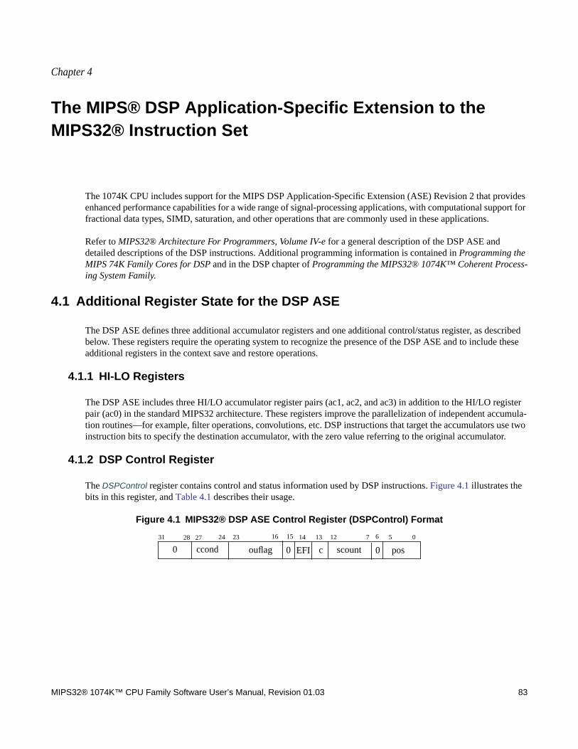
Chapter 4
MIPS32® 1074K™ CPU Family Software User’s Manual, Revision 01.03 83
The MIPS® DSP Application-Specific Extension to theMIPS32® Instruction Set
The 1074K CPU includes support for the MIPS DSP Application-Specific Extension (ASE) Revision 2 that providesenhanced performance capabilities for a wide range of signal-processing applications, with computational support forfractional data types, SIMD, saturation, and other operations that are commonly used in these applications.
Refer to MIPS32® Architecture For Programmers, Volume IV-e for a general description of the DSP ASE anddetailed descriptions of the DSP instructions. Additional programming information is contained in Programming theMIPS 74K Family Cores for DSP and in the DSP chapter of Programming the MIPS32® 1074K™ Coherent Process-ing System Family.
4.1 Additional Register State for the DSP ASE
The DSP ASE defines three additional accumulator registers and one additional control/status register, as describedbelow. These registers require the operating system to recognize the presence of the DSP ASE and to include theseadditional registers in the context save and restore operations.
4.1.1 HI-LO Registers
The DSP ASE includes three HI/LO accumulator register pairs (ac1, ac2, and ac3) in addition to the HI/LO registerpair (ac0) in the standard MIPS32 architecture. These registers improve the parallelization of independent accumula-tion routines—for example, filter operations, convolutions, etc. DSP instructions that target the accumulators use twoinstruction bits to specify the destination accumulator, with the zero value referring to the original accumulator.
4.1.2 DSP Control Register
The DSPControl register contains control and status information used by DSP instructions. Figure 4.1 illustrates thebits in this register, and Table 4.1 describes their usage.
Figure 4.1 MIPS32® DSP ASE Control Register (DSPControl) Format
scount
31 06
ouflag
7
0
121516
ccond pos
24 23 13
c
14
02728 5
0EFI

The MIPS® DSP Application-Specific Extension to the MIPS32® Instruction Set
84 MIPS32® 1074K™ CPU Family Software User’s Manual, Revision 01.03
Table 4.1 MIPS® DSP ASE Control Register (DSPControl) Field Descriptions
Fields
DescriptionRead /Write
ResetState ComplianceName Bits
0 31:28 Reserved. Used in the MIPS64 architecture but not usedin the MIPS32 architecture. Must be written as zero;returns zero on read.
0 0 Required
ccond 27:24 Condition code bits set by compare instructions. Thecompare instruction sets the right-most bits as requiredby the number of elements in the vector compare. Bitsnot set by the instruction remain unchanged.
R/W 0 Required
ouflag 23:16 This field is written by hardware when certain instruc-tions overflow or underflow and may have been satu-rated. See Table 4.2 for a full list of which bits are set bywhat instructions.
R/W 0 Required
EFI 14 Extract Fail Indicator. This bit is set to 1 when an EXTP,EXTPV, EXTPDP, or EXTPDP instruction fails. Theseinstructions fail when there are insufficient bits toextract, that is, when the value of pos in DSPControl isless than the value of size specified in the instruction.This bit is not sticky, so each invocation of one of thefour instructions will reset the bit depending on whetheror not the instruction failed.
R/W 0 Required
c 13 Carry bit. This bit is set and used by special add instruc-tions that implement a 64-bit add across two GPRs. TheADDSC instruction sets the bit and the ADDWCinstruction uses this bit.
R/W 0 Required
scount 12:7 This field is for use by the INSV instruction. The valueof this field is used to specify the size of the bit field tobe inserted.
R/W 0 Required
pos 5:0 This field is used by the variable insert instructionsINSV to specify the insert position.It is also used to indicate the extract position for theEXTP, EXTPV, EXTPDP, and EXTPDPV instructions.The decrement pos (DP) variants of these instructions oncompletion will have decremented the value of pos (bythe size amount).The MTHLIP instruction will increment the pos value by32 after copying the value of LO to HI.
R/W 0 Required
0 15:13 Must be written as zero; returns zero on read. 0 0 Reserved

4.2 Software Detection of the DSP ASE Revision 2
MIPS32® 1074K™ CPU Family Software User’s Manual, Revision 01.03 85
The bits of the overflow flag ouflag field in the DSPControl register are set by a number of instructions, as describedin Table 4.2. These bits are sticky and can be reset only by an explicit write to these bits in the register (using theWRDSP instruction).
4.2 Software Detection of the DSP ASE Revision 2
The presence of the MIPS DSP ASE in the 1074K CPU is indicated by two static bits in the Config3 register: theDSPP (DSP Present) bit indicates the presence of the DSP ASE, and the DSP2P (DSP Rev2 Present) bit indicatesthe presence of the MIPS DSP ASE Rev2. Because all members of the 1074K CPU family support both ASEs, thesebits are always set to 1.
The MX (DSP ASE Enable) read/write bit in the CP0 Status register must be set to enable access to the extra instruc-tions defined by the DSP ASE, as well as to the MTLO/HI, MFLO/HI instructions that access accumulators ac1, ac2,and ac3. Executing a DSP ASE instruction or the MTLO/HI, MFLO/HI instructions with this bit set to zero causes aDSP State Disabled Exception (exception code 26 in the CP0 Cause register). This exception can be used by systemsoftware to do lazy context-switching.
Table 4.2 DSPControl ouflag Bits
Bit Number Description
16 This bit is set when the destination is accumulator (HI-LO pair) zero, and an operation overflowor underflow occurs. These instructions are: DPAQ_S, DPAQ_SA, DPSQ_S, DPSQ_SA,DPAQX_S, DPAQX_SA, DPSQX_S, DPSQX_SA, MAQ_S, MAQ_SA and MULSAQ_S.
17 Same instructions as above, when the destination is accumulator (HI-LO pair) one.
18 Same instructions as above, when the destination is accumulator (HI-LO pair) two.
19 Same instructions as above, when the destination is accumulator (HI-LO pair) three.
20 Instructions that set this bit on an overflow/underflow: ABSQ_S, ADDQ, ADDQ_S, ADDU,ADDU_S, ADDWC, SUBQ, SUBQ_S, SUBU and SUBU_S.
21 Instructions that set this bit on an overflow/underflow: MUL, MUL_S, MULEQ_S, MULEU_S,MULQ_RS, and MULQ_S.
22 Instructions that set this bit on an overflow/underflow: PRECRQ_RS, SHLL, SHLL_S, SHLLV,and SHLLV_S.
23 Instructions that set this bit on an overflow/underflow: EXTR, EXTR_S, EXTR_RS, EXTRV,and EXTRV_RS.

The MIPS® DSP Application-Specific Extension to the MIPS32® Instruction Set
86 MIPS32® 1074K™ CPU Family Software User’s Manual, Revision 01.03

Chapter 5
MIPS32® 1074K™ CPU Family Software User’s Manual, Revision 01.03 87
Memory Management of the 1074K™ CPU
The 1074K CPU includes a Memory Management Unit (MMU) that interfaces between the execution unit and thecache controller. The CPU contains either a Translation Lookaside Buffer (TLB) or a simpler Fixed Mapping (FM)-style MMU, specified as a build-time option when the CPU is implemented.
This chapter contains the following sections:
• Section 5.1 “Introduction”
• Section 5.2 “Modes of Operation”
• Section 5.3 “Translation Lookaside Buffer”
• Section 5.4 “Virtual-to-Physical Address Translation”
• Section 5.5 “Fixed Mapping MMU”
5.1 Introduction
The MMU in a 1074K CPU translates a virtual address to a physical address before the request is sent to the cachecontrollers for tag comparison or to the bus interface unit for an external memory reference. Virtual-to-physicaladdress translation is especially useful for operating systems that must manage physical memory to accommodatemultiple tasks active in the same memory, and possibly in the same virtual address space (though, of course, in differ-ent locations in physical memory). The MMU also enforces the protection of memory areas and defines the cacheprotocols.
By default, the MMU is TLB-based. The TLB consists of two address-translation buffers: a dual-ported 16/32/48/64dual-entry fully associative Joint TLB (JTLB) and a 4-entry instruction micro TLB (ITLB). When an instructionaddress is translated, the ITLB is accessed first, and if the translation is not found, the JTLB is accessed. If there is amiss in the JTLB, an exception is taken. When a data reference is translated, the JTLB is accessed directly. If theaddress is not present in the JTLB, an exception is taken. The JTLB is dual-ported to prevent contention betweeninstruction and data accesses.
Optionally, the MMU can implement a Fixed Mapping (FM) mechanism, based on a simple algorithm that translatesvirtual addresses into physical addresses. These translations are different for various regions of the virtual addressspace.
Figure 5.1 shows how the MMU with TLB interacts with cache accesses, and Figure 5.2 shows the equivalent for theFM MMU.

Memory Management of the 1074K™ CPU
88 MIPS32® 1074K™ CPU Family Software User’s Manual, Revision 01.03
Figure 5.1 Address Translation For Cache Access with TLB MMU
Figure 5.2 Address Translation For Cache Access with FM MMU
Instruction VirtualAddress(IVA)
DataVirtual Address(DVA) JTLB
ITLB
InstructionCacheRAM
Data CacheRAM
IVA Entry
DataPhysical Address(DPA)
InstructionPhysical Address(IPA)
Tag (IPA)
Tag (DPA)
Comparator
Comparator
Data Hit/Miss
Instruction Hit/Miss
Instruction VirtualAddress(IVA)
DataVirtual Address(DVA)
FM MMU
InstructionCacheRAM
Data CacheRAM
DataPhysical Address(DPA)
InstructionPhysical Address(IPA)
Tag (IPA)
Tag (DPA)
Comparator
Comparator
Data Hit/Miss
Instruction Hit/Miss
FM MMU

5.2 Modes of Operation
MIPS32® 1074K™ CPU Family Software User’s Manual, Revision 01.03 89
5.2 Modes of Operation
The MMU’s virtual-to-physical address translation is determined by the mode in which the processor is operating. A1074K CPU operates in one of four modes:
• User mode
• Supervisor mode
• Kernel mode
• Debug mode
User mode is most often used for application programs. Supervisor mode is an intermediate privilege level withaccess to an additional region of memory and is only supported with the TLB-based MMU. Kernel mode is typicallyused for handling exceptions and privileged operating system functions, including CP0 management and I/O deviceaccesses. Debug mode is used for software debugging and usually occurs within a software development tool.
5.2.1 Virtual Memory Segments
The MIPS32 architecture supports a 4 GByte virtual address space that is partitioned into a number of segments, eachcharacterized by a set of attributes defined by hardware and software. The virtual memory segments are different
depending on the mode of operation. Figure 5.3 shows the segmentation for the 4 GByte (232 bytes) virtual memoryspace, addressed by a 32-bit virtual address, for each of the four modes.
User mode accesses are limited to a subset of the virtual address space (0x0000_0000 to 0x7FFF_FFFF) and can beinhibited from accessing CP0 functions. In User mode, virtual addresses 0x8000_0000 to 0xFFFF_FFFF are invalidand cause an exception if accessed. Supervisor mode adds access to sseg (0xC000_0000 to 0xDFFF_FFFF). kseg0,kseg1, and kseg3 will still cause exceptions if they are accessed. In Kernel mode, software has access to the entireaddress space, as well as all CP0 registers.
Debug mode is entered on a debug exception. While in Debug mode, the debug software has access to the sameaddress space and CP0 registers as Kernel mode. In addition, while in Debug mode, the CPU has access to the debugsegment (dseg). This area overlays part of the kernel segment kseg3. Access to dseg in Debug mode can be turned onor off, allowing full access to the entire kseg3 in Debug mode, if so desired.
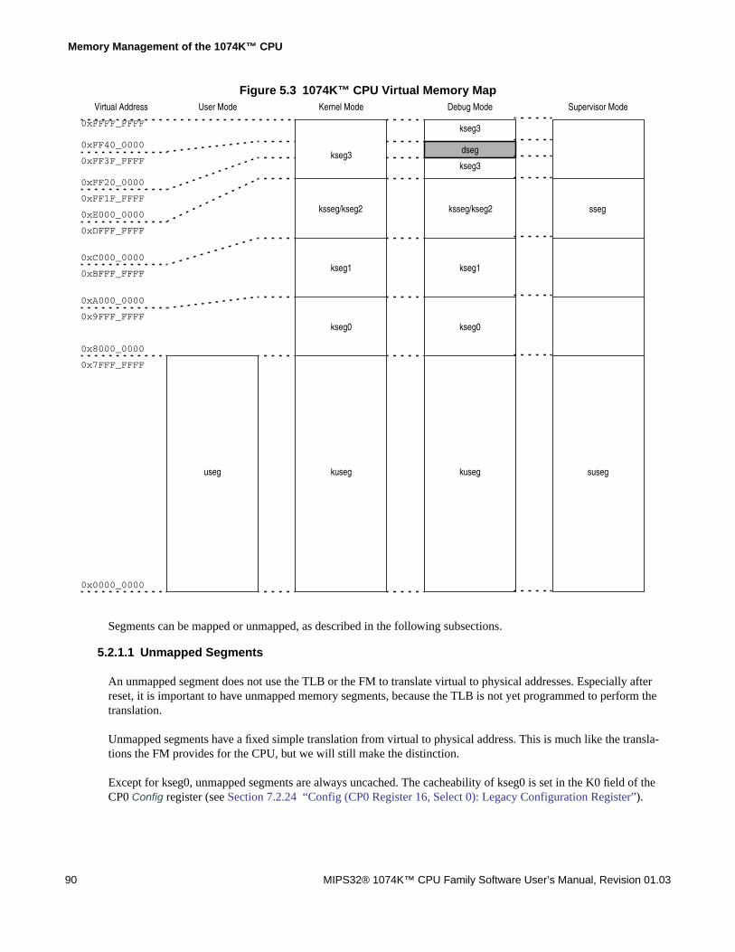
Memory Management of the 1074K™ CPU
90 MIPS32® 1074K™ CPU Family Software User’s Manual, Revision 01.03
Figure 5.3 1074K™ CPU Virtual Memory Map
Segments can be mapped or unmapped, as described in the following subsections.
5.2.1.1 Unmapped Segments
An unmapped segment does not use the TLB or the FM to translate virtual to physical addresses. Especially afterreset, it is important to have unmapped memory segments, because the TLB is not yet programmed to perform thetranslation.
Unmapped segments have a fixed simple translation from virtual to physical address. This is much like the transla-tions the FM provides for the CPU, but we will still make the distinction.
Except for kseg0, unmapped segments are always uncached. The cacheability of kseg0 is set in the K0 field of theCP0 Config register (see Section 7.2.24 “Config (CP0 Register 16, Select 0): Legacy Configuration Register”).
useg kuseg kuseg
kseg0
kseg1
ksseg/kseg2
kseg3
ksseg/kseg2
kseg1
kseg0
kseg3
kseg3
dseg
User Mode Kernel Mode Debug ModeVirtual Address
0x7FFF_FFFF
0x8000_0000
0x9FFF_FFFF
0xBFFF_FFFF
0xDFFF_FFFF
0xFF1F_FFFF
0xFF3F_FFFF
0xFFFF_FFFF
0xA000_0000
0xC000_0000
0xE000_0000
0xFF20_0000
0xFF40_0000
0x0000_0000
suseg
sseg
Supervisor Mode


Memory Management of the 1074K™ CPU
92 MIPS32® 1074K™ CPU Family Software User’s Manual, Revision 01.03
Table 5.1 lists the characteristics of the User mode segment.
All valid user mode virtual addresses have their most-significant bit cleared to 0, indicating that user mode can onlyaccess the lower half of the virtual memory map. All attempts to reference an address with the most-significant bit setwhile in user mode causes an address error exception.
All references to useg are mapped through the TLB or FM. For cores with a TLB, the virtual address is extended withthe contents of the 8-bit ASID field to form a unique virtual address before translation. Also, bit settings within theTLB entry for the page determine the cacheability of a reference. For FM MMU cores, the cacheability is set via theKU field of the CP0 Config register.
5.2.3 Supervisor Mode
In supervisor mode, two uniform virtual address spaces are available: a 2 GByte (231 bytes) virtual address spacecalled the supervisor user segment (suseg), and a 512 MByte virtual address space called the supervisor segment(sseg). The supervisor-mode virtual address space is shown in Figure 5.5.
Table 5.1 User Mode Segments
Address-BitValue
Status Register
SegmentName Address Range Segment Size
Bit Value
EXL ERL KSU
32-bitA(31) = 0
0 0 0b10 useg 0x0000_0000 -->0x7FFF_FFFF
2 GByte
(231 bytes)

5.2 Modes of Operation
MIPS32® 1074K™ CPU Family Software User’s Manual, Revision 01.03 93
Figure 5.5 Supervisor Mode Virtual Address Space
The supervisor user segment begins at address 0x0000_0000 and ends at address 0x7FFF_FFFF. The supervisor seg-ment begins at 0xC000_0000 and ends at 0xDFFF_FFFF. Accesses to all other addresses in Supervisor mode causean address error exception.
The processor operates in Supervisor mode when the Status register contains the following bit values:
• UM = 0 and SM= 1
• EXL = 0
• ERL = 0
In addition to the above values, the DM bit in the Debug register must be 0.
Address Error
suseg
kseg0
kseg1
sseg
kseg3
Mapped, 2048MB
Address Error
Supervisor virtual address spaceMapped, 512MB
Address Error
0x0000_0000
0x8000_0000
0xA000_0000
0xC000_0000
0xE000_0000
0x7FFF_FFFF
0x9FFF_FFFF
0xBFFF_FFFF
0xDFFF_FFFF
0xFFFF_FFFF

Memory Management of the 1074K™ CPU
94 MIPS32® 1074K™ CPU Family Software User’s Manual, Revision 01.03
Table 5.2 lists the characteristics of the Supervisor mode segments.
The system maps all references to suseg and sseg through the TLB or FM. For cores with a TLB, the virtual addressis extended with the contents of the 8-bit ASID field to form a unique virtual address before translation. Also, bit set-tings within the TLB entry for the page determine the cacheability of a reference. For FM MMU cores, the cacheabil-ity of suseg and sseg is set via the KU and K23 fields of the CP0 Config register respectively.
5.2.4 Kernel Mode
The processor operates in Kernel mode when the DM bit in the Debug register is 0 and the Status register contains oneor more of the following values:
• KSU = 0b00
• ERL = 1
• EXL = 1
When a non-debug exception is detected, EXL or ERL will be set and the processor will enter Kernel mode. At the endof the exception handler routine, an Exception Return (ERET) instruction is generally executed. The ERET instruc-tion jumps to the Exception PC, clears ERL, and clears EXL if ERL=0. This may return the processor to User mode.
In Kernel mode, a program has access to the entire virtual address space. Kernel mode virtual address space is dividedinto regions differentiated by the high-order bits of the virtual address, as shown in Figure 5.6. The characteristics ofkernel-mode segments are listed in Table 5.3.
The CPU enters Kernel mode both at reset and when an exception is recognized.
Table 5.2 Supervisor Mode Segments
Address-BitValue
Status Register
SegmentName Address Range Segment Size
Bit Value
EXL ERL UM SM
32-bitA(31) = 0
0 0 0 1 suseg 0x0000_0000 -->0x7FFF_FFFF
2 GByte
(231 bytes)
32-bitA(31:29) = 1102
0 0 0 1 sseg 0xC000_0000 ->0xDFFF_FFFF
512MB
(229 bytes)

5.2 Modes of Operation
MIPS32® 1074K™ CPU Family Software User’s Manual, Revision 01.03 95
Figure 5.6 Kernel Mode Virtual Address Space
Kernel virtual address spaceUnmapped, 512MB
kuseg
kseg0
kseg1
ksseg/kseg2
kseg3
Mapped, 2048MB
Kernel virtual address spaceUnmapped, Uncached, 512MB
Kernel virtual address spaceMapped, 512MB
Kernel virtual address spaceMapped, 512MB
0x0000_0000
0x8000_0000
0xA000_0000
0xC000_0000
0xE000_0000
0x7FFF_FFFF
0x9FFF_FFFF
0xBFFF_FFFF
0xDFFF_FFFF
0xFFFF_FFFF

Memory Management of the 1074K™ CPU
96 MIPS32® 1074K™ CPU Family Software User’s Manual, Revision 01.03
5.2.4.1 Kernel Mode, User Space (kuseg)
In Kernel mode, when the most-significant bit of the virtual address (A31) is cleared, the 32-bit kuseg virtual address
space is selected and covers the full 231 bytes (2 GBytes) of the current user address space mapped to addresses0x0000_0000 - 0x7FFF_FFFF. For cores with TLBs, the virtual address is extended with the contents of the 8-bitASID field to form a unique virtual address.
When ERL = 1 in the Status register, the user address region becomes a 231-byte unmapped and uncached addressspace. While in this setting, the kuseg virtual address maps directly to the same physical address, and does not includethe ASID field.
5.2.4.2 Kernel Mode, Kernel Space 0 (kseg0)
In Kernel mode, when the most-significant three bits of the virtual address are 1002, 32-bit kseg0 virtual address
space is selected; it is the 229-byte (512-MByte) kernel virtual space located at addresses 0x8000_0000 -0x9FFF_FFFF. References to kseg0 are unmapped; the physical address selected is defined by subtracting0x8000_0000 from the virtual address. The K0 field of the Config register controls cacheability.
5.2.4.3 Kernel Mode, Kernel Space 1 (kseg1)
In Kernel mode, when the most-significant three bits of the 32-bit virtual address are 1012, kseg1 virtual address
space is selected. kseg1 is the 229-byte (512-MByte) kernel virtual space located at addresses 0xA000_0000 -0xBFFF_FFFF. References to kseg1 are unmapped; the physical address selected is defined by subtracting0xA000_0000 from the virtual address. Caches are disabled for accesses to these addresses, and physical memory (ormemory-mapped I/O device registers) are accessed directly.
Table 5.3 Kernel Mode Segments
Address-BitValues
Status RegisterIs One of These
ValuesSegment
Name Address RangeSegment
SizeKSU EXL ERL
A(31) = 0 (KSU = 002
orEXL = 1
orERL = 1)
andDM = 0
kuseg 0x0000_0000through
0x7FFF_FFFF
2 GBytes (231 bytes)
A(31:29) = 1002 kseg0 0x8000_0000through
0x9FFF_FFFF
512 MBytes (229 bytes)
A(31:29) = 1012 kseg1 0xA000_0000through
0xBFFF_FFFF
512 MBytes (229 bytes)
A(31:29) = 1102 ksseg/kseg2 0xC000_0000through
0xDFFF_FFFF
512 MBytes (229 bytes)
A(31:29) = 1112 kseg3 0xE000_0000through
0xFFFF_FFFF
512 MBytes (229 bytes)
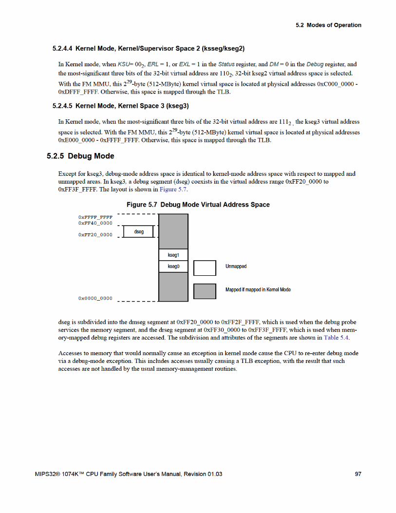

Memory Management of the 1074K™ CPU
98 MIPS32® 1074K™ CPU Family Software User’s Manual, Revision 01.03
The unmapped kseg0 and kseg1 segments from kernel-mode address space are available in debug mode, which allowsthe debug handler to be executed from uncached, unmapped memory.
5.2.5.1 Debug Mode, Register (drseg)
The behavior of CPU access to the drseg address range at 0xFF30_0000 to 0xFF3F_FFFF is determined as shown inTable 5.5
Debug software is expected to read the Debug Control register (DCR) to determine which other memory-mapped reg-isters exist in drseg. The value returned in response to a read of any unimplemented memory-mapped register isunpredictable, and writes are ignored to any unimplemented register in drseg. For more information about the DCR,refer to Chapter 11, “EJTAG Debug Support in the 1074K™ CPU”.
The allowed access size is limited for the drseg. Only word-size transactions are allowed. Operation of the processoris undefined for other transaction sizes.
5.2.5.2 Debug Mode, Memory (dmseg)
The conditions for CPU accesses to the dmseg address range (0xFF20_0000 to 0xFF2F_FFFF) are shown in Table5.6.
Table 5.4 Physical Address and Cache Attributes for dseg, dmseg, and drseg
SegmentName
Sub-SegmentName
VirtualAddress Generates Physical Address
CacheAttribute
dseg dmseg 0xFF20_0000through
0xFF2F_FFFF
dmseg maps to addresses 0x0_0000 -0xF_FFFF in EJTAG probe memoryspace.drseg maps to the breakpoint registers0x0_0000 - 0xF_FFFF
Uncached
drseg 0xFF30_0000through
0xFF3F_FFFF
Table 5.5 CPU Access to drseg
TransactionLSNM Bit in Debug
Register Access
Load / Store 1 Kernel mode address space (kseg3)
Fetch Don’t care drseg, see comments below
Load / Store 0
Table 5.6 CPU Access to dmseg
TransactionProbEn Bit inDCR Register
LSNM Bit inDebug Register Access
Load / Store Don’t care 1 Kernel mode address space (kseg3)
Fetch 1 Don’t care dmseg
Load / Store 1 0 dmseg
Fetch 0 Don’t care See comments below
Load / Store 0 0 See comments below


Memory Management of the 1074K™ CPU
100 MIPS32® 1074K™ CPU Family Software User’s Manual, Revision 01.03
Table 5.7 and Table 5.8 explain each of the fields in a JTLB entry.
Table 5.7 TLB Tag Entry Fields
Field Name Description
PageMask[28:13] Page Mask Value. The Page Mask defines the page size by masking the appropriateVPN2 bits from being involved in a comparison. It is also used to determine whichaddress bit is used to make the even-odd page (PFN0-PFN1) determination. See the tablebelow.
The PageMask column above shows all the legal values for PageMask. Because eachpair of bits can only have the same value, the physical entry in the JTLB will only save acompressed version of the PageMask using only 8 bits. This is however transparent tosoftware, which will always work with a 16 bit field
VPN2[31:13] Virtual Page Number divided by 2. This field contains the upper bits of the virtual pagenumber. Because it represents a pair of TLB pages, it is divided by 2. Bits 31:29 arealways included in the TLB lookup comparison. Bits 28:13 are included depending onthe page size, defined by PageMask
G Global Bit. When set, indicates that this entry is global to all processes and/or threadsand thus disables inclusion of the ASID in the comparison.
ASID[7:0] Address Space Identifier. Identifies which process or thread this TLB entry is associatedwith.
Table 5.8 TLB Data Entry Fields
Field Name Description
PFN0[31:12],PFN1[31:12]
Physical Frame Number. Defines the upper bits of the physical address.
PageMask Page Size Even/Odd Bank Select Bit
00_0000_0000_0000_00 4KB VAddr[12]
00_0000_0000_0000_11 16KB VAddr[14]
00_0000_0000_0011_11 64KB VAddr[16]
00_0000_0000_1111_11 256KB VAddr[18]
00_0000_0011_1111_11 1MB VAddr[20]
00_0000_1111_1111_11 4MB VAddr[22]
00_0011_1111_1111_11 16MB VAddr[24]
00_1111_1111_1111_11 64MB VAddr[26]
11_1111_1111_1111_11 256MB VAddr[28]

5.3 Translation Lookaside Buffer
MIPS32® 1074K™ CPU Family Software User’s Manual, Revision 01.03 101
In order to fill an entry in the JTLB, software executes a TLBWI or TLBWR instruction (see Section 5.4.3 “TLBInstructions”). Prior to invoking one of these instructions, several CP0 registers must be updated with the informationto be written to a TLB entry:
• PageMask is set in the CP0 PageMask register.
• VPN2, and ASID are set in the CP0 EntryHi register.
• PFN0, C0, D0, V0, and G bits are set in the CP0 EntryLo0 register.
• PFN1, C1, D1, V1, and G bits are set in the CP0 EntryLo1 register.
Note that the global bit “G” is part of both EntryLo0 and EntryLo1. The resulting “G” bit in the JTLB entry is the log-ical AND between the two fields in EntryLo0 and EntryLo1. Please refer to Chapter 7, “CP0 Registers of the 1074K™CPU” for further details.
The address space identifier (ASID) helps to reduce the frequency of TLB flushing on a context switch. The existenceof the ASID allows multiple processes to exist in both the TLB and instruction caches. The ASID value is stored inthe EntryHi register and is compared to the ASID value of each entry.
5.3.2 Instruction TLB
The ITLB is a 4-entry, fully-associative TLB dedicated to performing translations for the instruction stream. TheITLB only maps 4-Kbyte pages/sub-pages or 1-Mbyte pages/sub-pages.
C0[2:0],C1[2:0]
Cacheability. Contains an encoded value of the cacheability attributes and determineswhether the page should be placed in the cache or not. The field is encoded as follows:
D0,D1
“Dirty” or Write-enable Bit. Indicates that the page has been written and/or is writable. Ifthis bit is set, stores to the page are permitted. If the bit is cleared, stores to the pagecause a TLB Modified exception.
V0,V1
Valid Bit. Indicates that the TLB entry and, thus, the virtual page mapping are valid. Ifthis bit is set, accesses to the page are permitted. If the bit is cleared, accesses to the pagecause a TLB Invalid exception.
Table 5.8 TLB Data Entry Fields (Continued)
Field Name Description
C[2:0] Coherency Attribute
0 Reserved
1 Reserved
2 Uncached
3 Cacheable, noncoherent, write-back, write-allocate
4 Cacheable, coherent, write-back, write-allocate, exclusive
5 Cacheable, write-back, write-allocate, coherent, read misses requestShared
5 Cacheable, coherent, write-back, write-allocate, exclusive on write
6 Reserved
7 Uncached Accelerated


Memory Management of the 1074K™ CPU
104 MIPS32® 1074K™ CPU Family Software User’s Manual, Revision 01.03
Compared with previous cores from MIPS Technologies, the 1074K CPU uses a more relaxed check for multiplematches in order to avoid machine check exceptions while flushing or initializing the TLB. On a write, all matchingentries are disabled to prevent them from matching on future compares. A machine check is only signaled if the entrybeing written has its valid bit set, the matching entry in the TLB has its valid bit set, and the matching entry is not theentry being written. The cases for the signalling of the machine check exception are enumerated in Table 5.9.
5.4.2 Memory Space
To assist in controlling both the amount of mapped space and the replacement characteristics of various memoryregions, the 1074K CPU provides two mechanisms.
5.4.2.1 Page Sizes
First, the page size can be configured, on a per entry basis, to map different page sizes ranging from 4 KBytes to 256MBytes, in multiples of 4. The PageMask register is loaded with the desired page size, which is then entered into theTLB when a new entry is written. Thus, operating systems can provide special-purpose maps. For example, a typicalframe buffer can be memory-mapped with only one TLB entry.
The 1074K CPU implements the following page sizes:
4K, 16K, 64K, 256K, 1M, 4M, 16M, 64M, and 256M
Software can determine which page sizes are supported by writing all ones to the PageMask register, then reading thevalue back. For additional information, see Section 7.2.7 “PageMask (CP0 Register 5, Select 0): Control for VariablePage Size in TLB Entries”.
5.4.2.2 Replacement Algorithm
The second mechanism controls the replacement algorithm when a TLB miss occurs. TLB refill is often done usingthe TLBWR instruction to randomly replace one of the existing entries. The processor provides a mechanismwhereby a programmable number of mappings can be locked into the TLB via the CP0 Wired register, thus avoidingrandom replacement. Refer to Section 7.2.8 “Wired (CP0 Register 6, Select 0): Controls Number of Fixed ("wired")TLB Entries” for further details. For entries that are left available for random replacement, the CPU includes twoalgorithms for selecting the entry. One involves a counter that decrements almost every cycle (with some pseudo-ran-dom perturbation to minimize the likelihood of livelock conditions). A second scheme keeps a table of the TLBentries that have been most recently used and tries to avoid selecting one of them. Selection of the algorithm is donevia the CP0 Config6NMRUD bit.
Table 5.9 Machine Check Exception
ExistingMatch
Matching Entry equalsWritten Entry Existing Page Valid Bit Written Page Valid Bit
MachineCheck
No X X X No
Yes Yes X X No
Yes No 0 0 No
Yes No 0 1 No
Yes No 1 0 No
Yes No 1 1 Yes


Memory Management of the 1074K™ CPU
106 MIPS32® 1074K™ CPU Family Software User’s Manual, Revision 01.03
5.5 Fixed Mapping MMU
The 1074K CPU optionally implements a simple Fixed Mapping (FM) memory management unit that is smaller thanthe a full translation lookaside buffer (TLB) and more easily synthesized. Like a TLB, the FM performs virtual-to-physical address translation and provides attributes for the different memory segments. Those memory segmentswhich are unmapped in a TLB implementation (kseg0 and kseg1) are translated identically by the FM MMU.
The FM also determines the cacheability of each segment. These attributes are controlled via bits in the Config regis-ter. Table 5.11 shows the encoding for the K23 (bits 30:28), KU (bits 27:25) and K0 (bits 2:0) fields of the Config reg-ister.
With the FM MMU, no translation exceptions can be taken, although address errors are still possible.
TLBWI Translation Lookaside Buffer Write Index
TLBWR Translation Lookaside Buffer Write Random
Table 5.11 Cache Coherency Attributes
Config Register FieldsK23, KU, and K0 Cache Coherency Attribute
0 Reserved
1 Reserved
2 Uncached
3 Cacheable, noncoherent, write-back, write-allocate
4 Cacheable, write-back, write-allocate, coherent, read misses request Exclusive
5 Cacheable, write-back, write-allocate, coherent, read misses request Shared
6 Reserved
7 Uncached Accelerated
Table 5.12 Cacheability of Segments with Fixed Mapping Translation
SegmentVirtual Address
Range Cacheability
useg/kuseg 0x0000_0000-0x7FFF_FFFF
Controlled by the KU field (bits 27:25) of the Config register. Refer toTable 5.11 for the encoding.
kseg0 0x8000_0000-0x9FFF_FFFF
Controlled by the K0 field (bits 2:0) of the Config register. See Table5.11 for the encoding.
kseg1 0xA000_0000-0xBFFF_FFFF
Always uncacheable
kseg2 0xC000_0000-0xDFFF_FFFF
Controlled by the K23 field (bits 30:28) of the Config register. Refer toTable 5.11 for the encoding.
kseg3 0xE000_0000-0xFFFF_FFFF
Controlled by K23 field (bits 30:28) of the Config register. Refer toTable 5.11 for the encoding.
Table 5.10 TLB Instructions (Continued)
Op Code Description of Instruction


Chapter 6
MIPS32® 1074K™ CPU Family Software User’s Manual, Revision 01.03 109
Exceptions and Interrupts in the 1074K™ CPU
The 1074K CPU receives exceptions from a number of sources, including arithmetic overflows, misses in the transla-tion lookaside buffer (TLB), I/O interrupts, and system calls. When the CPU detects an exception, the normalsequence of instruction execution is suspended and the processor enters kernel mode, disables interrupts, loads theException Program Counter (EPC) register with the location where execution can restart after the exception has beenserviced, and forces execution of a software exception handler located at a specific address.
The software exception handler saves the context of the processor, including the contents of the program counter, thecurrent operating mode, and the status of the interrupts (enabled or disabled). This context is saved so it can berestored when the exception has been serviced.
Exceptions may be precise or imprecise. Precise exceptions are those for which the EPC can be used to identify theinstruction that caused the exception. For precise exceptions, the restart location in the EPC register is the address ofthe instruction that caused the exception or, if the instruction was executing in a branch delay slot (as indicated by theBD bit in the Cause register), the address of the branch instruction immediately preceding the delay slot. Impreciseexceptions, on the other hand, are those for which no return address can be identified. Bus error exceptions and CP2exceptions are examples of imprecise exceptions.
This chapter contains the following sections:
• Section 6.1 “Exception Conditions”
• Section 6.2 “Exception Priority”
• Section 6.3 “Interrupts”
• Section 6.4 “GPR Shadow Registers”
• Section 6.5 “Exception Vector Locations”
• Section 6.6 “General Exception Processing”
• Section 6.7 “Debug Exception Processing”
• Section 6.8 “Exception Descriptions”
• Section 6.9 “Exception Handling and Servicing Flowcharts”
6.1 Exception Conditions
When an exception condition occurs, the instruction causing the exception and all those that follow it in the pipelineare cancelled. Accordingly, any stall conditions and any later exception conditions that may have referenced thisinstruction are inhibited.

Exceptions and Interrupts in the 1074K™ CPU
110 MIPS32® 1074K™ CPU Family Software User’s Manual, Revision 01.03
When the exception condition is detected on an instruction fetch, the CPU aborts that instruction and all instructionsthat follow. When this instruction reaches the WB stage, the exception flag causes it to write various CP0 registerswith the exception state, change the current program counter (PC) to the appropriate exception vector address, andclear the exception bits of earlier pipeline stages.
For most types of exceptions, this implementation allows all preceding instructions to complete execution and pre-vents all subsequent instructions from completing. Thus, the value in the EPC (or ErrorEPC for errors or DEPC fordebug exceptions) is sufficient to restart execution. It also ensures that exceptions are taken in the order of execu-tion—an instruction taking an exception may itself be killed by an instruction further down the pipeline that takes anexception in a later cycle.
Imprecise exceptions are taken after the instruction that caused them has completed and potentially after followinginstructions have completed.
6.2 Exception Priority
Table 6.1 contains a list and a brief description of all exception conditions, The exceptions are listed in the order oftheir relative priority, from highest priority (Reset) to lowest priority (Load/store bus error). When several exceptionsoccur simultaneously, the exception with the highest priority is taken.
Table 6.1 Priority of Exceptions
Exception Description
Reset Assertion of SI_Reset signal.
DSS EJTAG Debug Single Step.
DINT EJTAG Debug Interrupt. Caused by the assertion of the external EJ_DINT input, orby setting the EjtagBrk bit in the ECR register.
DDBLImpr/DDBSImpr Debug Data Break Load/Store. Imprecise.
NMI Asserting edge of SI_NMI signal.
Machine Check TLB write that conflicts with an existing entry.
Interrupt Assertion of unmasked hardware or software interrupt signal.
Deferred Watch Deferred Watch (unmasked by K|DM->!(K|DM) transition).
DIB EJTAG debug hardware instruction break matched.
WATCH A reference to an address in one of the watch registers (fetch).
AdEL Fetch address alignment error.Fetch reference to protected address.
TLBL Fetch TLB miss.Fetch TLB hit to page with V=0.
I-cache Error Parity error on I-cache access.
IBE Instruction fetch bus error.
DBp EJTAG Breakpoint (execution of SDBBP instruction).
Sys Execution of SYSCALL instruction.
Bp Execution of BREAK instruction.
CpU Execution of a coprocessor instruction for a coprocessor that is not enabled.
CEU Execution of a CorExtend instruction modifying local state when CorExtend is notenabled.

6.3 Interrupts
MIPS32® 1074K™ CPU Family Software User’s Manual, Revision 01.03 111
6.3 Interrupts
In the MIPS32® Release 1 architecture, support for exceptions included two software interrupts, six hardware inter-rupts, and a special-purpose timer interrupt. The timer interrupt was provided external to the CPU and was typicallycombined with hardware interrupt 5 in a system-dependent manner. Interrupts were handled either through the gen-eral exception vector (offset 0x180) or the special interrupt vector (0x200), based on the value of CauseIV. Softwarewas required to prioritize interrupts as a function of the CauseIV bits in the interrupt handler prologue.
Release 2 of the Architecture, implemented by the 1074K CPU, adds a number of upward-compatible extensions tothe Release 1 interrupt architecture, including support for vectored interrupts and the implementation of a new inter-rupt mode that permits the use of an external interrupt controller.
Additionally, internal performance counters have been added to the 1074K CPU. These counters can be configured tocount various events within the CPU. When the MSB of the counter is set, it can trigger a performance counter inter-rupt. This interrupt, like the timer interrupt, is an output from the CPU that can be brought back into the CPU’s inter-rupt pins in a system-dependent manner.
The Fast Debug Channel feature in EJTAG provides a low overhead means for sending data between CPU softwareand the EJTAG probe. It includes a pair of FIFOs for transmit and receive data. Software can define FIFO thresholdsfor generating an interrupt. The fast debug channel interrupt is also routed similarly to the timer and performancecounter interrupts. The interrupt status is made available on an output pin and can be brought back into the CPU’sinterrupt pins.
DSPDis DSP ASE State Disabled.
RI Execution of a Reserved Instruction.
FPE Floating Point exception.
Ov Execution of an arithmetic instruction that overflowed.
Tr Execution of a trap (when trap condition is true).
DDBL / DDBS EJTAG Data Address Break (address only).
WATCH A reference to an address in one of the watch registers (data).
AdEL Load address alignment error.Load reference to protected address.
AdES Store address alignment error.Store to protected address.
TLBL Load TLB miss.Load TLB hit to page with V=0
TLBS Store TLB miss.Store TLB hit to page with V=0.
TLB Mod Store to TLB page with D=0.
D-cache Error Cache parity error. Imprecise.
DBE Load or store bus error. Imprecise.
Table 6.1 Priority of Exceptions (Continued)
Exception Description

Exceptions and Interrupts in the 1074K™ CPU
112 MIPS32® 1074K™ CPU Family Software User’s Manual, Revision 01.03
6.3.1 Interrupt Modes
The 1074K CPU includes support for three interrupt modes, as defined by Release 2 of the Architecture:
• Interrupt Compatibility mode, in which the behavior of the 1074K is identical to the behavior of an implementa-tion of Release 1 of the Architecture.
• Vectored Interrupt (VI) mode, which adds the ability to prioritize and vector interrupts to a handler dedicated tothat interrupt, and to assign a GPR shadow set for use during interrupt processing. The presence of this mode isdenoted by the VInt bit in the Config3 register. Although this mode is architecturally optional, it is always presenton the 1074K CPU, so the VInt bit will always read as a 1.
• External Interrupt Controller (EIC) mode, which redefines the way interrupts are handled to provide full supportfor an external interrupt controller that handles prioritization and vectoring of interrupts. As with VI mode, thismode is architecturally optional. The presence of this mode is denoted by the VEIC bit in the Config3 register. Onthe 1074K CPU, the VEIC bit is set externally by the static input, SI_EICPresent, to allow system logic to indi-cate the presence of an external interrupt controller.
Following reset, the 1074K processor defaults to Compatibility mode, which is fully compatible with all implementa-tions of Release 1 of the Architecture.
Table 6.2 shows the current interrupt mode of the processor as a function of the Coprocessor 0 register fields that canaffect the mode.
6.3.1.1 Interrupt Compatibility Mode
This is the default interrupt mode for the processor and is entered when a Reset exception occurs. In this mode, inter-rupts are non-vectored and dispatched though exception vector offset 0x180 (if CauseIV = 0) or vector offset 0x200 (ifCause IV = 1). This mode is in effect when any of the following conditions are true:
• CauseIV = 0
• StatusBEV = 1
Table 6.2 Interrupt Modes
Sta
tusB
EV
Cau
seIV
IntC
tlVS
Con
fig3V
INT
Con
fig3V
EIC
Interrupt Mode
1 x x x x Compatibility
x 0 x x x Compatibility
x x =0 x x Compatibility
0 1 ≠0 1 0 Vectored Interrupt
0 1 ≠0 x 1 External Interrupt Controller
0 1 ≠0 0 0 Cannot occur because IntCtl VS cannot be non-zero if neither Vectored Inter-
rupt nor External Interrupt Controller mode is implemented.
“x” denotes don’t care

6.3 Interrupts
MIPS32® 1074K™ CPU Family Software User’s Manual, Revision 01.03 113
• IntCtlVS = 0, which is the case if vectored interrupts are not implemented or have been disabled.
Here is a typical software handler for compatibility mode:
/* * Assumptions: * - CauseIV = 1 (if it were zero, the interrupt exception would have to * be isolated from the general exception vector before arriving * here) * - GPRs k0 and k1 are available (no shadow register switches invoked in * compatibility mode) * - The software priority is IP7..IP0 (HW5..HW0, SW1..SW0) * * Location: Offset 0x200 from exception base */
IVexception:mfc0 k0, C0_Cause /* Read Cause register for IP bits */mfc0 k1, C0_Status /* and Status register for IM bits */andi k0, k0, M_CauseIM /* Keep only IP bits from Cause */and k0, k0, k1 /* and mask with IM bits */beq k0, zero, Dismiss /* no bits set - spurious interrupt */clz k0, k0 /* Find first bit set, IP7..IP0; k0 = 16..23 */xori k0, k0, 0x17 /* 16..23 => 7..0 */sll k0, k0, VS /* Shift to emulate software IntCtlVS */la k1, VectorBase /* Get base of 8 interrupt vectors */addu k0, k0, k1 /* Compute target from base and offset */jr k0 /* Jump to specific exception routine */nop
/* * Each interrupt processing routine processes a specific interrupt, analogous * to those reached in VI or EIC interrupt mode. Since each processing routine * is dedicated to a particular interrupt line, it has the context to know * which line was asserted. Each processing routine may need to look further * to determine the actual source of the interrupt if multiple interrupt requests * are ORed together on a single IP line. Once that task is performed, the * interrupt may be processed in one of two ways: * * - Completely at interrupt level (e.g., a simple UART interrupt). The * SimpleInterrupt routine below is an example of this type. * - By saving sufficient state and re-enabling other interrupts. In this * case the software model determines which interrupts are disabled during * the processing of this interrupt. Typically, this is either the single * StatusIM bit that corresponds to the interrupt being processed, or some * collection of other StatusIM bits so that “lower” priority interrupts are * also disabled. The NestedInterrupt routine below is an example of this type. */
SimpleInterrupt:/* * Process the device interrupt here and clear the interupt request * at the device. In order to do this, some registers may need to be * saved and restored. The coprocessor 0 state is such that an ERET * will simply return to the interrupted code. */
eret /* Return to interrupted code */
Exceptions and Interrupts in the 1074K™ CPU
114 MIPS32® 1074K™ CPU Family Software User’s Manual, Revision 01.03
NestedException:/* * Nested exceptions typically require saving the EPC and Status registers, * saving any GPRs that may be modified by the nested exception routine, disabling * the appropriate IM bits in Status to prevent an interrupt loop, putting * the processor in kernel mode, and re-enabling interrupts. The sample code * below cannot cover all nuances of this processing and is intended only * to demonstrate the concepts. */
/* Save GPRs here, and setup software context */mfc0 k0, C0_EPC /* Get restart address */s k0, EPCSave /* Save in memory */mfc0 k0, C0_Status /* Get Status value */sw k0, StatusSave /* Save in memory */li k1, ~IMbitsToClear /* Get IM bits to clear for this interrupt */
/* this must include at least the IM bit *//* for the current interrupt, and may include *//* others */
and k0, k0, k1 /* Clear bits in copy of Status */ins k0, zero, S_StatusEXL, (W_StatusKSU+W_StatusERL+W_StatusEXL)
/* Clear KSU, ERL, EXL bits in k0 */mtc0 k0, C0_Status /* Modify mask, switch to kernel mode, */
/* re-enable interrupts */
/* * Process interrupt here, including clearing device interrupt. * In some environments this may be done with a thread running in * kernel or user mode. Such an environment is well beyond the scope of * this example. */
/* * To complete interrupt processing, the saved values must be restored * and the original interrupted code restarted. */
di /* Disable interrupts - may not be required */lw k0, StatusSave /* Get saved Status (including EXL set) */l k1, EPCSave /* and EPC */mtc0 k0, C0_Status /* Restore the original value */mtc0 k1, C0_EPC /* and EPC *//* Restore GPRs and software state */eret /* Dismiss the interrupt */
6.3.1.2 Vectored Interrupt Mode
In Vectored Interrupt (VI) mode, a priority encoder prioritizes pending interrupts and generates a vector which can beused to direct each interrupt to a dedicated handler routine. This mode also allows each interrupt to be mapped to aGPR shadow register set for use by the interrupt handler. VI mode is in effect when all the following conditions aretrue:
• Config3VInt = 1
• Config3VEIC = 0
• IntCtlVS ≠ 0
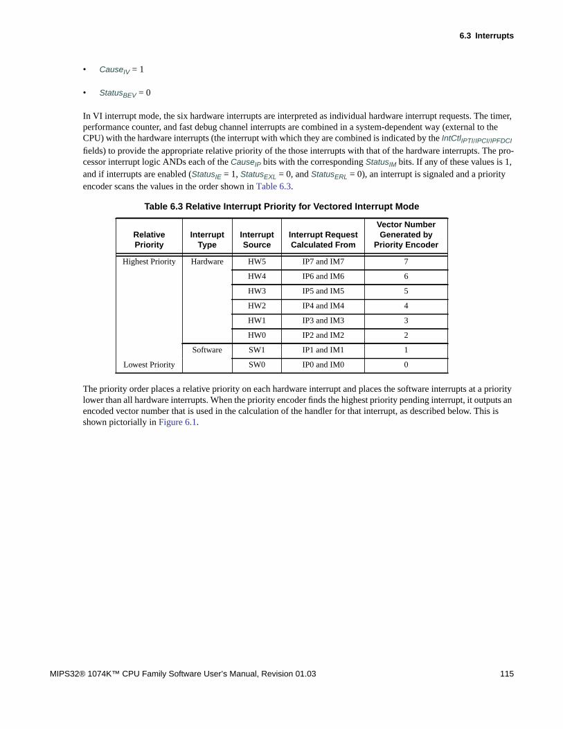
6.3 Interrupts
MIPS32® 1074K™ CPU Family Software User’s Manual, Revision 01.03 115
• CauseIV = 1
• StatusBEV = 0
In VI interrupt mode, the six hardware interrupts are interpreted as individual hardware interrupt requests. The timer,performance counter, and fast debug channel interrupts are combined in a system-dependent way (external to theCPU) with the hardware interrupts (the interrupt with which they are combined is indicated by the IntCtlIPTI/IPCI/IPFDCI
fields) to provide the appropriate relative priority of the those interrupts with that of the hardware interrupts. The pro-cessor interrupt logic ANDs each of the CauseIP bits with the corresponding StatusIM bits. If any of these values is 1,and if interrupts are enabled (StatusIE = 1, StatusEXL = 0, and StatusERL = 0), an interrupt is signaled and a priorityencoder scans the values in the order shown in Table 6.3.
The priority order places a relative priority on each hardware interrupt and places the software interrupts at a prioritylower than all hardware interrupts. When the priority encoder finds the highest priority pending interrupt, it outputs anencoded vector number that is used in the calculation of the handler for that interrupt, as described below. This isshown pictorially in Figure 6.1.
Table 6.3 Relative Interrupt Priority for Vectored Interrupt Mode
RelativePriority
InterruptType
InterruptSource
Interrupt RequestCalculated From
Vector NumberGenerated by
Priority Encoder
Highest Priority Hardware HW5 IP7 and IM7 7
HW4 IP6 and IM6 6
HW3 IP5 and IM5 5
HW2 IP4 and IM4 4
HW1 IP3 and IM3 3
HW0 IP2 and IM2 2
Software SW1 IP1 and IM1 1
Lowest Priority SW0 IP0 and IM0 0


6.3 Interrupts
MIPS32® 1074K™ CPU Family Software User’s Manual, Revision 01.03 117
/* for the current interrupt, and may include *//* others */
and k0, k0, k1 /* Clear bits in copy of Status *//* If switching shadow sets, write new value to SRSCtlPSS here */ins k0, zero, S_StatusEXL, (W_StatusKSU+W_StatusERL+W_StatusEXL)
/* Clear KSU, ERL, EXL bits in k0 */mtc0 k0, C0_Status /* Modify mask, switch to kernel mode, */
/* re-enable interrupts *//* * If switching shadow sets, clear only KSU above, write target * address to EPC, and do execute an eret to clear EXL, switch * shadow sets, and jump to routine */
/* Process interrupt here, including clearing device interrupt */
/* * To complete interrupt processing, the saved values must be restored * and the original interrupted code restarted. */
di /* Disable interrupts - may not be required */lw k0, StatusSave /* Get saved Status (including EXL set) */l k1, EPCSave /* and EPC */mtc0 k0, C0_Status /* Restore the original value */lw k0, SRSCtlSave /* Get saved SRSCtl */mtc0 k1, C0_EPC /* and EPC */mtc0 k0, C0_SRSCtl /* Restore shadow sets */ehb /* Clear hazard */eret /* Dismiss the interrupt */
6.3.1.3 External Interrupt Controller Mode
External Interrupt Controller (EIC) mode redefines the way that the processor interrupt logic is configured to providesupport for an external interrupt controller. The interrupt controller is responsible for prioritizing all interrupts,including hardware, software, timer, fast debug channel, and performance counter interrupts, and directly supplyingto the processor the vector number of the highest priority interrupt.
EIC interrupt mode is in effect if all of the following conditions are true:
• Config3VEIC = 1
• IntCtlVS ≠ 0
• CauseIV = 1
• StatusBEV = 0
In EIC mode, the processor sends the state of the software interrupt requests (CauseIP1..IP0) and the timer, perfor-mance counter, and fast debug channel interrupt requests (CauseTI/PCI/FDCI) to the external interrupt controller, whichprioritizes these interrupts in a system-dependent way with other hardware interrupts. The interrupt controller can bea hardwired logic block, or it can be configurable by control and status registers. This allows the interrupt controllerto be more specific or more general as a function of the system environment and needs.

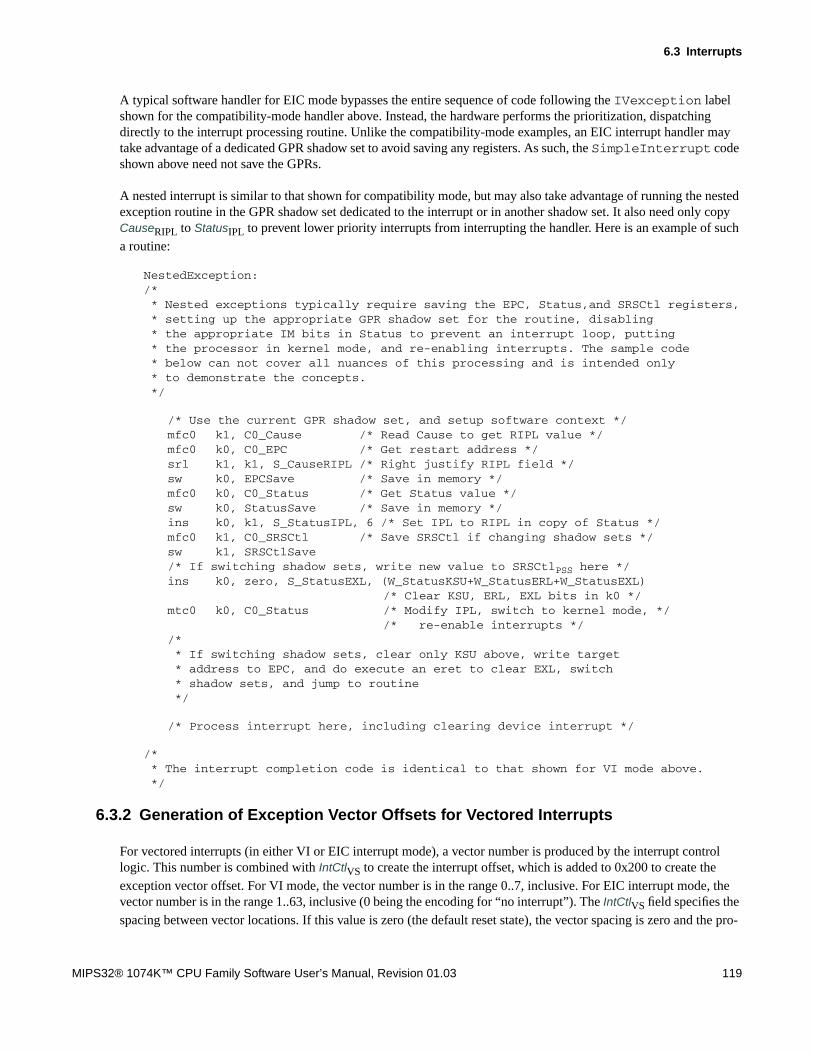
6.3 Interrupts
MIPS32® 1074K™ CPU Family Software User’s Manual, Revision 01.03 119
A typical software handler for EIC mode bypasses the entire sequence of code following the IVexception labelshown for the compatibility-mode handler above. Instead, the hardware performs the prioritization, dispatchingdirectly to the interrupt processing routine. Unlike the compatibility-mode examples, an EIC interrupt handler maytake advantage of a dedicated GPR shadow set to avoid saving any registers. As such, the SimpleInterrupt codeshown above need not save the GPRs.
A nested interrupt is similar to that shown for compatibility mode, but may also take advantage of running the nestedexception routine in the GPR shadow set dedicated to the interrupt or in another shadow set. It also need only copyCauseRIPL to StatusIPL to prevent lower priority interrupts from interrupting the handler. Here is an example of sucha routine:
NestedException:/* * Nested exceptions typically require saving the EPC, Status,and SRSCtl registers, * setting up the appropriate GPR shadow set for the routine, disabling * the appropriate IM bits in Status to prevent an interrupt loop, putting * the processor in kernel mode, and re-enabling interrupts. The sample code * below can not cover all nuances of this processing and is intended only * to demonstrate the concepts. */
/* Use the current GPR shadow set, and setup software context */mfc0 k1, C0_Cause /* Read Cause to get RIPL value */mfc0 k0, C0_EPC /* Get restart address */srl k1, k1, S_CauseRIPL /* Right justify RIPL field */sw k0, EPCSave /* Save in memory */mfc0 k0, C0_Status /* Get Status value */sw k0, StatusSave /* Save in memory */ins k0, k1, S_StatusIPL, 6 /* Set IPL to RIPL in copy of Status */mfc0 k1, C0_SRSCtl /* Save SRSCtl if changing shadow sets */sw k1, SRSCtlSave/* If switching shadow sets, write new value to SRSCtlPSS here */ins k0, zero, S_StatusEXL, (W_StatusKSU+W_StatusERL+W_StatusEXL)
/* Clear KSU, ERL, EXL bits in k0 */mtc0 k0, C0_Status /* Modify IPL, switch to kernel mode, */
/* re-enable interrupts *//* * If switching shadow sets, clear only KSU above, write target * address to EPC, and do execute an eret to clear EXL, switch * shadow sets, and jump to routine */
/* Process interrupt here, including clearing device interrupt */
/* * The interrupt completion code is identical to that shown for VI mode above. */
6.3.2 Generation of Exception Vector Offsets for Vectored Interrupts
For vectored interrupts (in either VI or EIC interrupt mode), a vector number is produced by the interrupt controllogic. This number is combined with IntCtlVS to create the interrupt offset, which is added to 0x200 to create theexception vector offset. For VI mode, the vector number is in the range 0..7, inclusive. For EIC interrupt mode, thevector number is in the range 1..63, inclusive (0 being the encoding for “no interrupt”). The IntCtlVS field specifies thespacing between vector locations. If this value is zero (the default reset state), the vector spacing is zero and the pro-

Exceptions and Interrupts in the 1074K™ CPU
120 MIPS32® 1074K™ CPU Family Software User’s Manual, Revision 01.03
cessor reverts to Interrupt Compatibility mode. A non-zero value enables vectored interrupts. Table 6.4 shows theexception vector offset for a representative subset of the vector numbers and values of the IntCtlVS field.
The general equation for the exception vector offset for a vectored interrupt is:
vectorOffset ← 0x200 + (vectorNumber × (IntCtlVS || 0b00000))
6.3.3 Global Interrupt Controller
The Global Interrupt Controller (GIC) is an optional feature of the 1074K Coherent Processing System. This block
handles the routing and masking of VPE-local1 interrupts, such as the timer, performance counter, fast debug channelinterrupts, inter-processor interrupts, and external interrupts. This block can be configured to support various numbersof external interrupts and to support any of the CPU interrupt modes.
An interactive GUI is available to simplify the setup of desired event-routing through the GIC. The tool outputs a C-language function covering all required programming registers of the GIC.
For a detailed description of the GIC, refer to [5].
6.4 GPR Shadow Registers
Release 2 of the Architecture optionally removes the need to save and restore GPRs on entry to high-priority inter-rupts and exceptions, and to provide specified processor modes with the same capability. This is done by introducingmultiple copies of the GPRs, called shadow sets, and by allowing privileged software to associate a shadow set withentry to kernel mode via an interrupt vector or exception. The normal GPRs are designated as shadow set zero.
Table 6.4 Exception Vector Offsets for Vectored Interrupts
Vector Number
Value of IntCtlVS Field
0b00001 0b00010 0b00100 0b01000 0b10000
0 0x0200 0x0200 0x0200 0x0200 0x0200
1 0x0220 0x0240 0x0280 0x0300 0x0400
2 0x0240 0x0280 0x0300 0x0400 0x0600
3 0x0260 0x02C0 0x0380 0x0500 0x0800
4 0x0280 0x0300 0x0400 0x0600 0x0A00
5 0x02A0 0x0340 0x0480 0x0700 0x0C00
6 0x02C0 0x0380 0x0500 0x0800 0x0E00
7 0x02E0 0x03C0 0x0580 0x0900 0x1000
•••
61 0x09A0 0x1140 0x2080 0x3F00 0x7C00
62 0x09C0 0x1180 0x2100 0x4000 0x7E00
63 0x09E0 0x11C0 0x2180 0x4100 0x8000
1. The GIC is designed to work with CPUs that have more than one Virtual Processing Element (VPE) per CPU. However, each1074K CPU effectively behaves like one VPE per CPU. Thus there is a one-to-one mapping of CPUs to VPEs.

6.4 GPR Shadow Registers
MIPS32® 1074K™ CPU Family Software User’s Manual, Revision 01.03 121
The number of GPR shadow sets is a build-time option on the 1074K CPU. Although Release 2 of the Architecturedefines a maximum of 16 shadow sets, the CPU allows one (the normal GPRs), two, or four shadow sets. The highestnumber actually implemented is indicated by the SRSCtlHSS field. If this field is zero, only the normal GPRs areimplemented.
Shadow sets are new copies of the GPRs that can be substituted for the normal GPRs on entry to kernel mode via aninterrupt or exception. Once a shadow set is bound to a kernel mode entry condition, reference to GPRs operateexactly as one would expect, but they are redirected to registers that are dedicated to that condition. Privileged soft-ware may need to reference all GPRs in the register file, even specific shadow registers that are not visible in the cur-rent mode. The RDPGPR and WRPGPR instructions are used for this purpose. The CSS field of the SRSCtl registerprovides the number of the current shadow register set, and the PSS field of the SRSCtl register provides the numberof the previous shadow register set (the set that was current before the last exception or interrupt occurred).
If the processor is operating in VI mode, binding of a vectored interrupt to a shadow set is done by writing to theSRSMap register. If the processor is operating in EIC interrupt mode, the binding of the interrupt to a specific shadowset is provided by the external interrupt controller, and is configured in an implementation-dependent way. Binding ofan exception or non-vectored interrupt to a shadow set is done by writing to the ESS field of the SRSCtl register.When an exception or interrupt occurs, the value of SRSCtlCSS is copied to SRSCtlPSS, and SRSCtlCSS is set to thevalue taken from the appropriate source. On an ERET, the value of SRSCtlPSS is copied back into SRSCtlCSS torestore the shadow set of the mode to which control returns. More precisely, the rules for updating the fields in theSRSCtl register on an interrupt or exception are as follows:
1. No field in the SRSCtl register is updated if any of the following conditions are true (in this case, steps 2 and 3are skipped):
• The exception is one that sets StatusERL: Reset or NMI.
• The exception causes entry into EJTAG Debug Mode
• StatusBEV = 1
• StatusEXL = 1
2. SRSCtlCSS is copied to SRSCtlPSS
3. SRSCtlCSS is updated from one of the following sources:
• The appropriate field of the SRSMap register, based on IPL, if the exception is an interrupt, CauseIV = 1,Config3VEIC = 0, and Config3VInt = 1. These are the conditions for a vectored interrupt.
• The EICSS field of the SRSCtl register if the exception is an interrupt, CauseIV = 1, and Config3VEIC = 1.These are the conditions for a vectored EIC interrupt.
• The ESS field of the SRSCtl register in any other case. This is the condition for a non-interrupt exception, ora non-vectored interrupt.
Similarly, the rules for updating the fields in the SRSCtl register at the end of an exception or interrupt are as follows:
1. No field in the SRSCtl register is updated if any of the following conditions are true (in this case, step 2 isskipped):
• A DERET is executed

Exceptions and Interrupts in the 1074K™ CPU
122 MIPS32® 1074K™ CPU Family Software User’s Manual, Revision 01.03
• An ERET is executed with StatusERL = 1
2. SRSCtlPSS is copied to SRSCtlCSS.
These rules have the effect of preserving the SRSCtl register in any case of a nested exception or one which occursbefore the processor has been fully initialized (StatusBEV = 1).
Privileged software may switch the current shadow set by writing a new value into SRSCtlPSS, loading EPC with atarget address, and doing an ERET.
6.5 Exception Vector Locations
The Reset, Soft Reset, NMI, and EJTAG Debug exceptions are vectored to a specific location, as shown in Table 6.5and Table 6.6. Addresses for all other exceptions are a combination of a vector offset and a vector base address. InRelease 1 of the architecture, the vector base address was fixed. In Release 2, software is allowed to specify the vectorbase address via the EBase register for exceptions that occur when StatusBEV equals 0. Another degree of flexibilityin the selection of the vector base address, for use when StatusBEV equals 1, is provided via a set of input pins,SI_UseExceptionBase and SI_ExceptionBase[29:12]. Table 6.5 shows the vector base address whenSI_UseExceptionBase equals 0, as a function of the exception and whether the BEV bit is set in the Status register.Table 6.6 shows the vector base addresses when SI_UseExceptionBase = 1. As can be seen in Table 6.6, whenSI_UseExceptionBase equals 1, the exception vectors for cases where StatusBEV = 0 are not affected.
In the 1074K Coherent Processing System, SI_UseExceptionBase is tied to 1, and the SI_ExceptionBase input is pro-grammable via settings in the Global Configuration Register. The default value of the control register matches theCPU behavior if SI_UseExceptionBase had been set to 0. Refer to [5] for more details.
Table 6.7 shows the offsets from the vector base address as a function of the exception. Note that the IV bit in theCause register causes interrupts to use a dedicated exception vector offset, rather than the general exception vector.Table 6.4 (on page 120) shows the offset from the base address in the case where StatusBEV = 0 and CauseIV = 1.Table 6.8 combines these two tables into one that contains all possible vector addresses as a function of the state thatcan affect the vector selection. To avoid complexity in the table, it is assumed that IntCtlVS = 0.
Table 6.5 Exception Vector Base Addresses, SI_UseExceptionBase = 0
Exception
StatusBEV
0 1
Reset, NMI 0xBFC0.0000
EJTAG Debug (with ProbEn = 0, inthe EJTAG_Control_register andDCR.RDVec=0)
0xBFC0.0480
EJTAG Debug (with ProbEn = 0, inthe EJTAG_Control_register andDCR.RDVec=1)
0x DebugVectorAddr[31:7] || 2b0000000
EJTAG Debug (with ProbEn = 1 inthe EJTAG_Control_register)
0xFF20.0200
Cache Error EBase31 30 || 1 ||EBase28 12 || 0x000
Note that EBase31 30 have the fixed value
0b10
0xBFC0.0300

6.5 Exception Vector Locations
MIPS32® 1074K™ CPU Family Software User’s Manual, Revision 01.03 123
Other EBase31 12 || 0x000Note that EBase31 30 have the fixed value
0b10
0xBFC0.0200
‘||’ denotes bit string concatenation
Table 6.6 Exception Vector Base Addresses, SI_UseExceptionBase = 1
Exception
StatusBEV
0 1
Reset, NMI 0b10 || SI_ExceptionBase [29:12] || 0x000
EJTAG Debug (with ProbEn = 0in the EJTAG_Control_register andDCR.RDVec=0)
DebugVectorAddr[31:7] || 2b0000000
EJTAG Debug (with ProbEn = 0in the EJTAG_Control_register andDCR.RDVec=1)
0b10 ||SI_ExceptionBase[29:12] || 0x480
EJTAG Debug (with ProbEn = 1in the EJTAG_Control_register)
0xFF20.0200
Cache Error EBase31 30 || 1 ||EBase28 12 || 0x000
Note that EBase31 30 have the
fixed value 0b10
0b101 ||SI_ExceptionBase[28:12] ||0x300
Other EBase31 12 || 0x000Note that EBase31 30 have the
fixed value 0b10
0b10 ||SI_ExceptionBase[29:12] ||0x200
‘||’ denotes bit string concatenation
Table 6.7 Exception Vector Offsets
Exception Vector Offset
TLB Refill, EXL = 0 0x000
General Exception 0x180
Interrupt, CauseIV = 1 0x200 (In Release 2 implementa-tions, this is the base of the vectoredinterrupt table when StatusBEV = 0)
Reset, NMI None (uses reset base address)
Table 6.5 Exception Vector Base Addresses, SI_UseExceptionBase = 0
Exception
StatusBEV
0 1

Exceptions and Interrupts in the 1074K™ CPU
124 MIPS32® 1074K™ CPU Family Software User’s Manual, Revision 01.03
6.6 General Exception Processing
With the exception of Reset, NMI, cache error, and EJTAG Debug exceptions, which have their own special process-ing as described below, exceptions have the same basic processing flow:
Table 6.8 Exception Vectors
Exception SI_
Use
Exc
epti
on
Bas
e
Sta
tus B
EV
Sta
tus E
XL
Cau
seIV
EJT
AG
Pro
bE
n
Vector(IntCtlVS = 0)
Reset, NMI 0 x x x x 0xBFC0.0000
Reset, NMI 1 x x x x 0b10 || SI_ExceptionBase[29:12] || 0x000
EJTAG Debug 0 x x x 0 0xBFC0.0480 (if DCR.RDVec=0)DebugVectorAddr[31:7] || 2b0000000 (if DCR.RDVec=1)
EJTAG Debug 1 x x x 0 0b10 || SI_ExceptionBase[29:12] || 0x480 (if DCR.RDVec=0)DebugVectorAddr[31:7] || 2b0000000 (if DCR.RDVec=1)
EJTAG Debug x x x x 1 0xFF20.0200
TLB Refill 0 0 1 x x 0xEBase[31:12] || 0x180
TLB Refill 0 1 0 x x 0xBFC0.0200
TLB Refill 1 1 0 x x 0b10 || SI_ExceptionBase[29:12] || 0x200
TLB Refill 0 1 1 x x 0xBFC0.0380
TLB Refill 1 1 1 x x 0b10 || SI_ExceptionBase[29:12] || 0x380
Cache Error 0 0 x x x 0xEBase[31:30] || 0b1 || EBase[28:12] || 0x100
Cache Error 0 1 x x x 0xBFC0.0300
Cache Error 1 1 x x x 0b101 || SI_ExceptionBase[28:12] || 0x300
Interrupt x 0 0 0 x 0xEBase[31:12] || 0x180
Interrupt x 0 0 1 x 0xEBase[31:12] || 0x200
Interrupt 0 1 0 0 x 0xBFC0.0380
Interrupt 1 1 0 0 x 0b10 || SI_ExceptionBase[29:12] || 0x380
Interrupt 0 1 0 1 x 0xBFC0.0400
Interrupt 1 1 0 1 x 0b10 || SI_ExceptionBase[29:12] || 0x400
All others 0 0 x x x 0xEBase[31:12] || 0x180
All others 0 1 x x x 0xBFC0.0380
All others 1 1 x x x 0b10 || SI_ExceptionBase[29:12] || 0x380
‘x’ denotes don’t care,‘||’ denotes bit string concatenation

6.6 General Exception Processing
MIPS32® 1074K™ CPU Family Software User’s Manual, Revision 01.03 125
• If the EXL bit in the Status register is zero, the EPC register is loaded with the PC at which execution will berestarted, and the BD bit is set appropriately in the Cause register (see Table 7.25). The value loaded into theEPC register is dependent on whether the processor implements the MIPS16 ASE, and whether the instruction isin the delay slot of a branch or jump which has delay slots. Table 6.9 shows the value stored in each of the CP0PC registers, including EPC. For implementations of Release 2 of the Architecture if StatusBEV = 0, the CSS
field in the SRSCtl register is copied to the PSS field, and the CSS value is loaded from the appropriate source.
If the EXL bit in the Status register is set, the EPC register is not loaded and the BD bit is not changed in theCause register. For implementations of Release 2 of the Architecture, the SRSCtl register is not changed.
• The CE, and ExcCode fields of the Cause registers are loaded with the values appropriate to the exception. TheCE field is loaded, but not defined, for any exception type other than a coprocessor unusable exception.
• The EXL bit is set in the Status register.
• The processor begins executing at the exception vector.
The value loaded into EPC represents the restart address for the exception and need not be modified by exceptionhandler software in the normal case. Software need not look at the BD bit in the Cause register unless it wishes toidentify the address of the instruction that actually caused the exception.
Note that individual exception types may load additional information into other registers. This is noted in the descrip-tion of each exception type below.
Operation:
/* If StatusEXL is 1, all exceptions go through the general exception vector *//* and neither EPC nor CauseBD nor SRSCtl are modified */if StatusEXL = 1 then
vectorOffset ← 0x180else
/* For implementations that include the MIPS16e ASE, calculate potential *//* PC adjustment for exceptions in the delay slot */if Config1CA = 0 then
restartPC ← PCbranchAdjust ← 4 /* Possible adjustment for delay slot */
elserestartPC ← PC..1 || ISAModeif (ISAMode = 0) or ExtendedMIPS16Instruction
branchAdjust ← 4 /* Possible adjustment for 32-bit MIPS delay slot */else
branchAdjust ← 2 /* Possible adjustment for MIPS16 delay slot */
Table 6.9 Value Stored in EPC, ErrorEPC, or DEPC on Exception
MIPS16Implemented?
In Branch/JumpDelay Slot? Value stored in EPC/ErrorEPC/DEPC
No No Address of the instruction
No Yes Address of the branch or jump instruction (PC-4)
Yes No Upper 31 bits of the address of the instruction, combinedwith the ISA Mode bit
Yes Yes Upper 31 bits of the branch or jump instruction (PC-2 inthe MIPS16 ISA Mode and PC-4 in the 32-bit ISA Mode),combined with the ISA Mode bit

Exceptions and Interrupts in the 1074K™ CPU
126 MIPS32® 1074K™ CPU Family Software User’s Manual, Revision 01.03
endifendifif InstructionInBranchDelaySlot then
EPC ← restartPC - branchAdjust/* PC of branch/jump */CauseBD ← 1
elseEPC ← restartPC /* PC of instruction */CauseBD ← 0
endif
/* Compute vector offsets as a function of the type of exception */NewShadowSet ← SRSCtlESS /* Assume exception, Release 2 only */if ExceptionType = TLBRefill then
vectorOffset ← 0x000elseif (ExceptionType = Interrupt) then
if (CauseIV = 0) thenvectorOffset ← 0x180
elseif (StatusBEV = 1) or (IntCtlVS = 0) then
vectorOffset ← 0x200else
if Config3VEIC = 1 thenVecNum ← CauseRIPLNewShadowSet ← SRSCtlEICSS
elseVecNum ← VIntPriorityEncoder()NewShadowSet ← SRSMapIPL×4+3..IPL×4
endifvectorOffset ← 0x200 + (VecNum × (IntCtlVS || 0b00000))
endif /* if (StatusBEV = 1) or (IntCtlVS = 0) then */endif /* if (CauseIV = 0) then */
endif /* elseif (ExceptionType = Interrupt) then */
/* Update the shadow set information for an implementation of *//* Release 2 of the architecture */if ((ArchitectureRevision ≥ 2) and (SRSCtlHSS > 0) and (StatusBEV = 0) and
(StatusERL = 0)) thenSRSCtlPSS ← SRSCtlCSSSRSCtlCSS ← NewShadowSet
endifendif /* if StatusEXL = 1 then */
CauseCE ← FaultingCoprocessorNumberCauseExcCode ← ExceptionTypeStatusEXL ← 1
if Config1CA = 1 thenISAMode ← 0
endif
/* Calculate the vector base address */if StatusBEV = 1 then
vectorBase ← 0xBFC0.0200else
if ArchitectureRevision ≥ 2 then/* The fixed value of EBase31..30 forces the base to be in kseg0 or kseg1 */vectorBase ← EBase31..12 || 0x000
else

6.7 Debug Exception Processing
MIPS32® 1074K™ CPU Family Software User’s Manual, Revision 01.03 127
vectorBase ← 0x8000.0000endif
endif
/* Exception PC is the sum of vectorBase and vectorOffset */PC ← vectorBase..30 || (vectorBase29..0 + vectorOffset29..0)
/* No carry between bits 29 and 30 */
6.7 Debug Exception Processing
All debug exceptions have the same basic processing flow:
• The DEPC register is loaded with the program counter (PC) value at which execution will be restarted and theDBD bit is set appropriately in the Debug register. The value loaded into the DEPC register is the current PC if theinstruction is not in the delay slot of a branch, or the PC-4 of the branch if the instruction is in the delay slot of abranch.
• The DSS, DBp, DDBL, DDBS, DIB, and DINT bits (D* bits [5:0]) in the Debug register are updated appropriately,depending on the debug exception type.
• Halt and Doze bits in the Debug register are updated appropriately.
• The DM bit in the Debug register is set to 1.
• The processor is started at the debug exception vector.
The value loaded into DEPC represents the restart address for the debug exception and need not be modified by thedebug exception handler software in the usual case. Debug software need not look at the DBD bit in the Debug regis-ter unless it wishes to identify the address of the instruction that actually caused the debug exception.
A unique debug exception is indicated through the DSS, DBp, DDBL, DDBS, DIB and DINT bits (D* bits [5:0]) in theDebug register.
No other CP0 registers or fields are changed due to the debug exception, and thus no additional state is saved.
Operation:
if InstructionInBranchDelaySlot thenDEPC ← PC-4DebugDBD ← 1
elseDEPC ← PCDebugDBD ← 0
endifDebugD* bits at at [5:0] ← DebugExceptionTypeDebugHalt ← HaltStatusAtDebugExceptionDebugDoze ← DozeStatusAtDebugExceptionDebugDM ← 1if EJTAGControlRegisterProbTrap = 1 then
PC ← 0xFF20_0200else
if DebugControlRegisterRDVec = 1 thenif CacheErr then
PC ← 2#101 || DebugVectorAddr28..7 || 2#0000000else

Exceptions and Interrupts in the 1074K™ CPU
128 MIPS32® 1074K™ CPU Family Software User’s Manual, Revision 01.03
PC ← 2#10 || DebugVectorAddr29..7 || 2#0000000else
if SI_UseExceptionBaseif CacheErr then
PC ← 2#101 || SI_ExceptionBase[28:12] || 0x000else
PC ← 2#10 || SI_ExceptionBase[29:12] || 0x000else
PC ← 0xBFC0_0480endif
The location of the debug exception vector is determined by the ProbTrap bit in the EJTAG Control register (ECR) andthe RDVec bit in the Debug Control register (DCR), as shown in Table 6.10.
The value in the optional drseg register DebugVectorAddr (offset 0x00020) is used as the debug exception vectorwhen the ECR ProbTrap bit is 0 and when enabled through the optional RDVec control bit in the Debug ControlRegister (DCR). Bit 0 of DebugVectorAddr determines the ISA mode used to execute the handler. Figure 6.3 showsthe format of the DebugVectorAddr register; Table 6.11 describes the DebugVectorAddr register fields.
Figure 6.3 DebugVectorAddr Register Format
Bits 31..30 of the DebugVectorAddr register are fixed with the value 0b10, and the addition of the base address and theexception offset is done inhibiting a carry between bit 29 and bit 30 of the final exception address. The combinationof these two restrictions forces the final exception address to be in the kseg0 or kseg1 unmapped virtual address seg-ments. For cache error exceptions, bit 29 is forced to a 1 in the ultimate exception base address, so that this exceptionalways runs in the kseg1 unmapped, uncached virtual address segment.
When MIPS16 is implemented, the power-up state of IM is zero. If the implementation does not include MIPS16, theIM field is read-only, should be written with zero and will return 0 on a read.
Table 6.10 Debug Exception Vector Addresses
ProbTrap bit in ECRRegister
RDVec bit inDCR Register Debug Exception Vector Address
0 0 0xBFC0 0480
0 1 DebugVectorAddr31 7 || 0000000
1 0 0xFF20 0200 in dmseg
1 1
31 30 29 7 6 0
1 0 DebugVectorOffset 0 IM
Table 6.11 DebugVectorAddr Register Field Descriptions
Fields
Description Read / Write Reset StateName Bit(s)
1 31 Ignored on write; returns one on read. R 1
DebugVectorOffset 29:7 Programmable Debug Exception Vector Offset R/W Preset to0x7F8009
IM 0 ISA mode to be used for exception handler R 0
0 30,6:1 Ignored on write; returns zero on read. R 0

6.8 Exception Descriptions
MIPS32® 1074K™ CPU Family Software User’s Manual, Revision 01.03 129
If the TAP is not implemented, the debug exception vector location is as if ProbTrap=0.
6.8 Exception Descriptions
The following subsections describe each of the exceptions listed in the same sequence as shown in Table 6.1.
6.8.1 Reset Exception
A reset exception occurs when the SI_Reset signal is asserted to the processor. This exception is not maskable. Whena Reset exception occurs, the processor performs a full reset initialization, including aborting state machines, estab-lishing critical state, and generally placing the processor in a state in which it can execute instructions from uncached,unmapped address space. On a Reset exception, the state of the processor is not defined, with the following excep-tions:
• The Random register is initialized to the number of TLB entries - 1.
• The Wired register is initialized to zero.
• The Config register is initialized with its boot state.
• The RP, BEV, TS, SR, NMI, and ERL fields of the Status register are initialized to a specified state.
• The I, R, and W fields of the WatchLo register are initialized to 0.
• The ErrorEPC register is loaded with PC-4 if the state of the processor indicates that it was executing an instruc-tion in the delay slot of a branch. Otherwise, the ErrorEPC register is loaded with PC. Note that this value may ormay not be predictable.
• PC is loaded with 0xBFC0_0000.
Cause Register ExcCode Value:
None
Additional State Saved:
None
Entry Vector Used:
Reset (0xBFC0_0000)
Operation:
Random ← TLBEntries - 1Wired ← 0Config ← ConfigurationStateStatusRP ← 0StatusBEV ← 1StatusTS ← 0StatusSR ← 0StatusNMI ← 0StatusERL ← 1WatchLoI ← 0WatchLoR ← 0WatchLoW ← 0

Exceptions and Interrupts in the 1074K™ CPU
130 MIPS32® 1074K™ CPU Family Software User’s Manual, Revision 01.03
if InstructionInBranchDelaySlot thenErrorEPC ← PC - 4
elseErrorEPC ← PC
endifPC ← 0xBFC0_0000
6.8.2 Debug Single Step Exception
A debug single step exception occurs after the CPU has executed one/two instructions in non-debug mode, whenreturning to non-debug mode after debug mode. One instruction is allowed to execute when returning to a non-jump/branch instruction, otherwise two instructions are allowed to execute since the jump/branch and the instruction in thedelay slot are executed as one step. Debug single step exceptions are enabled by the SSt bit in the Debug register, andare always disabled for the first one/two instructions after a DERET.
The DEPC register points to the instruction on which the debug single step exception occurred, which is also the nextinstruction to single step or execute when returning from debug mode. So the DEPC register will not point to theinstruction which has just been single stepped, but rather the following instruction. The DBD bit in the Debug registeris never set for a debug single step exception, since the jump/branch and the instruction in the delay slot is executed inone step.
Exceptions occurring on the instruction(s) executed with debug single step exception enabled are taken even thoughdebug single step was enabled. For a normal exception (other than reset), a debug single step exception is then takenon the first instruction in the normal exception handler. Debug exceptions are unaffected by single step mode, e.g.returning to a SDBBP instruction with debug single step exceptions enabled causes a debug software breakpointexception, and DEPC will point to the SDBBP instruction. However, returning to an instruction (not jump/branch)just before the SDBBP instruction, causes a debug single step exception with DEPC pointing to the SDBBP instruc-tion.
To ensure proper functionality of single step, the debug single step exception has priority over all other exceptions,except reset and soft reset.
Debug Register Debug Status Bit Set
DSS
Additional State Saved
None
Entry Vector Used
Debug exception vector
6.8.3 Debug Interrupt Exception
A debug interrupt exception is either caused by the EjtagBrk bit in the EJTAG Control register (controlled through theTAP), or caused by the debug interrupt request signal to the CPU.
The debug interrupt exception is an asynchronous debug exception which is taken as soon as possible, but with nospecific relation to the executed instructions. The DEPC register is set to the instruction where execution should con-tinue after the debug handler is through. The DBD bit is set based on whether the interrupted instruction was execut-ing in the delay slot of a branch.

6.8 Exception Descriptions
MIPS32® 1074K™ CPU Family Software User’s Manual, Revision 01.03 131
Debug Register Debug Status Bit Set
DINT
Additional State Saved
None
Entry Vector Used
Debug exception vector
6.8.4 Non-Maskable Interrupt (NMI) Exception
A non maskable interrupt exception occurs when the SI_NMI signal is asserted to the processor. SI_NMI is an edgesensitive signal - only one NMI exception will be taken each time it is asserted. An NMI exception occurs only atinstruction boundaries, so it does not cause any reset or other hardware initialization. The state of the cache, memory,and other processor states are consistent and all registers are preserved, with the following exceptions:
• The BEV, TS, SR, NMI, and ERL fields of the Status register are initialized to a specified state.
• The ErrorEPC register is loaded with PC-4 if the state of the processor indicates that it was executing an instruc-tion in the delay slot of a branch. Otherwise, the ErrorEPC register is loaded with PC.
• PC is loaded with 0xBFC0_0000.
Cause Register ExcCode Value:
None
Additional State Saved:
None
Entry Vector Used:
Reset (0xBFC0_0000)
Operation:
StatusBEV ← 1StatusTS ← 0StatusSR ← 0StatusNMI ← 1StatusERL ← 1if InstructionInBranchDelaySlot then
ErrorEPC ← PC - 4else
ErrorEPC ← PCendifPC ← 0xBFC0_0000
6.8.5 Machine Check Exception
A machine check exception occurs when the processor detects an internal inconsistency. The following conditioncauses a machine check exception:

Exceptions and Interrupts in the 1074K™ CPU
132 MIPS32® 1074K™ CPU Family Software User’s Manual, Revision 01.03
• The detection of multiple matching entries in the TLB. The CPU detects this condition on a TLB write and pre-vents the write from being completed. The TS bit in the Status register is set to indicate this condition. This bit isonly a status flag and does not affect the operation of the device. Software clears this bit at the appropriate time.This condition is resolved by flushing the conflicting TLB entries. The TLB write can then be completed.
Cause Register ExcCode Value:
MCheck
Additional State Saved:
None
Entry Vector Used:
General exception vector (offset 0x180)
6.8.6 Interrupt Exception
The interrupt exception occurs when one or more of the six hardware, two software, or timer interrupt requests isenabled by the Status register and the interrupt input is asserted. See 6.3 “Interrupts” on page 111 for more detailsabout the processing of interrupts.
Register ExcCode Value:
Int
Additional State Saved:
Entry Vector Used:
See 6.3.2 “Generation of Exception Vector Offsets for Vectored Interrupts” on page 119 for the entry vector used,depending on the interrupt mode the processor is operating in.
6.8.7 Debug Instruction Break Exception
A debug instruction break exception occurs when an instruction hardware breakpoint matches an executed instruc-tion. The DEPC register and DBD bit in the Debug register indicate the instruction that caused the instruction hard-ware breakpoint to match. This exception can only occur if instruction hardware breakpoints are implemented.
Debug Register Debug Status Bit Set:
DIB
Additional State Saved:
None
Entry Vector Used:
Debug exception vector
Table 6.12 Register States an Interrupt Exception
Register State Value
CauseIP Indicates the interrupts that are pending.

6.8 Exception Descriptions
MIPS32® 1074K™ CPU Family Software User’s Manual, Revision 01.03 133
6.8.8 Watch Exception — Instruction Fetch or Data Access
The Watch facility provides a software debugging vehicle by initiating a watch exception when an instruction or datareference matches the address information stored in the WatchHi and WatchLo registers. A Watch exception is takenimmediately if the EXL and ERL bits of the Status register are both zero and the DM bit of the Debug register is alsozero. If any of those bits is a one at the time that a watch exception would normally be taken, then the WP bit in theCause register is set, and the exception is deferred until all three bits are zero. Software may use the WP bit in theCause register to determine if the EPC register points at the instruction that caused the watch exception, or if theexception actually occurred while in kernel mode.
The Watch exception can occur on either an instruction fetch or a data access. Watch exceptions that occur on aninstruction fetch have a higher priority than watch exceptions that occur on a data access.
Register ExcCode Value:
WATCH
Additional State Saved:
Entry Vector Used:
General exception vector (offset 0x180)
6.8.9 Address Error Exception — Instruction Fetch/Data Access
An address error exception occurs on an instruction or data access when an attempt is made to execute one of the fol-lowing:
• Fetch an instruction, load a word, or store a word that is not aligned on a word boundary
• Load or store a halfword that is not aligned on a halfword boundary
• Reference the kernel address space from user mode
Note that in the case of an instruction fetch that is not aligned on a word boundary, PC is updated before the conditionis detected. Therefore, both EPC and BadVAddr point to the unaligned instruction address. In the case of a data accessthe exception is taken if either an unaligned address or an address that was inaccessible in the current processor modewas referenced by a load or store instruction.
Cause Register ExcCode Value:
ADEL: Reference was a load or an instruction fetch
ADES: Reference was a store
Table 6.13 Register States on Watch Exception
Register State Value
CauseWP Indicates that the watch exception was deferred until afterStatusEXL, StatusERL, and DebugDM were zero. This bit
directly causes a watch exception, so software must clearthis bit as part of the exception handler to prevent a watchexception loop at the end of the current handler execution.
WatchHi I,R,W Set for the watch channel that matched, and indicateswhich type of match there was.

Exceptions and Interrupts in the 1074K™ CPU
134 MIPS32® 1074K™ CPU Family Software User’s Manual, Revision 01.03
Additional State Saved:
Entry Vector Used:
General exception vector (offset 0x180)
6.8.10 TLB Refill Exception — Instruction Fetch or Data Access
During an instruction fetch or data access, a TLB refill exception occurs when no TLB entry matches a reference to amapped address space and the EXL bit is 0 in the Status register. Note that this is distinct from the case in which anentry matches but has the valid bit off. In that case, a TLB Invalid exception occurs.
Cause Register ExcCode Value:
TLBL: Reference was a load or an instruction fetch
TLBS: Reference was a store
Additional State Saved:
Entry Vector Used:
TLB refill vector (offset 0x000) if StatusEXL = 0 at the time of exception;
General exception vector (offset 0x180) if StatusEXL = 1 at the time of exception
6.8.11 TLB Invalid Exception — Instruction Fetch or Data Access
During an instruction fetch or data access, a TLB invalid exception occurs in one of the following cases:
• No TLB entry matches a reference to a mapped address space; and the EXL bit is 1 in the Status register.
Table 6.14 CP0 Register States on Address Exception Error
Register State Value
BadVAddr Failing address
ContextVPN2 UNPREDICTABLE
EntryHiVPN2 UNPREDICTABLE
EntryLo0 UNPREDICTABLE
EntryLo1 UNPREDICTABLE
Table 6.15 CP0 Register States on TLB Refill Exception
Register State Value
BadVAddr Failing address.
Context The BadVPN2 field contains VA31:13 of the failing
address.
EntryHi The VPN2 field contains VA31:13 of the failing address;
the ASID field contains the ASID of the reference thatmissed.
EntryLo0 UNPREDICTABLE
EntryLo1 UNPREDICTABLE

6.8 Exception Descriptions
MIPS32® 1074K™ CPU Family Software User’s Manual, Revision 01.03 135
• A TLB entry matches a reference to a mapped address space, but the matched entry has the valid bit off.
Cause Register ExcCode Value:
TLBL: Reference was a load or an instruction fetch
TLBS: Reference was a store
Additional State Saved:
Entry Vector Used:
General exception vector (offset 0x180)
6.8.12 Cache Error Exception
A cache error exception occurs when an instruction or data reference detects a cache tag or data error. This exceptionis not maskable. Because the error was in a cache, the exception vector is to an unmapped, uncached address. Thisexception can be imprecise and the ErrorEPC may not point to the instruction that saw the errorAdditionally, becausethe caches on the cores within the 1074K Coherent Processing System are coherent, cache errors detected on othercores could indicate data corruption for a process on this CPU. An error on another CPU will still cause a Cache Errorexception, with the CacheErrEE indicating that the error occurred on another processor.
L2 cache errors are considered to be imprecise. An L2 cache error on a data load operation can potentially corrupt thetarget GPR.
Cause Register ExcCode Value
N/A
Additional State Saved
Entry Vector Used
Cache error vector (offset 0x100)
Table 6.16 CP0 Register States on TLB Invalid Exception
Register State Value
BadVAddr Failing address
Context The BadVPN2 field contains VA31:13 of the failing
address.
EntryHi The VPN2 field contains VA31:13 of the failing address;
the ASID field contains the ASID of the reference thatmissed.
EntryLo0 UNPREDICTABLE
EntryLo1 UNPREDICTABLE
Table 6.17 CP0 Register States on Cache Error Exception
Register State Value
CacheErr Error state
ErrorEPC Restart PC

Exceptions and Interrupts in the 1074K™ CPU
136 MIPS32® 1074K™ CPU Family Software User’s Manual, Revision 01.03
6.8.13 Bus Error Exception — Instruction Fetch or Data Access
A bus error exception occurs when an instruction or data access makes a bus request (due to a cache miss or anuncacheable reference) and that request terminates in an error. The bus error exception can occur on either an instruc-tion fetch or a data read. Bus error exceptions cannot be generated on data writes. Bus error exceptions that occur onan instruction fetch have a higher priority than bus error exceptions that occur on a data access.
Instruction errors are precise, will Data bus errors can be imprecise. These errors are taken when the ERR code isreturned on the OC_SResp input.
Cause Register ExcCode Value:
IBE: Error on an instruction reference
DBE: Error on a data reference
Additional State Saved:
None
Entry Vector Used:
General exception vector (offset 0x180)
6.8.14 Debug Software Breakpoint Exception
A debug software breakpoint exception occurs when an SDBBP instruction is executed. The DEPC register and DBDbit in the Debug register will indicate the SDBBP instruction that caused the debug exception.
Debug Register Debug Status Bit Set:
DBp
Additional State Saved:
None
Entry Vector Used:
Debug exception vector
6.8.15 Execution Exception — System Call
The system call exception is one of the execution exceptions. All of these exceptions have the same priority. A systemcall exception occurs when a SYSCALL instruction is executed.
Cause Register ExcCode Value:
Sys
Additional State Saved:
None
Entry Vector Used:
General exception vector (offset 0x180)

6.8 Exception Descriptions
MIPS32® 1074K™ CPU Family Software User’s Manual, Revision 01.03 137
6.8.16 Execution Exception — Breakpoint
The breakpoint exception is one of the execution exceptions. All of these exceptions have the same priority. A break-point exception occurs when a BREAK instruction is executed.
Cause Register ExcCode Value:
Bp
Additional State Saved:
None
Entry Vector Used:
General exception vector (offset 0x180)
6.8.17 Execution Exception — Reserved Instruction
The reserved instruction exception is one of the execution exceptions. All of these exceptions have the same priority.A reserved instruction exception occurs when a reserved or undefined major opcode or function field is executed.This includes Coprocessor 2 instructions which are decoded reserved in the Coprocessor 2.
Cause Register ExcCode Value:
RI
Additional State Saved:
None
Entry Vector Used:
General exception vector (offset 0x180)
6.8.18 Execution Exception — Coprocessor Unusable
The coprocessor unusable exception is one of the execution exceptions. All of these exceptions have the same prior-ity. A coprocessor unusable exception occurs when an attempt is made to execute a coprocessor instruction for one ofthe following:
• a corresponding coprocessor unit that has not been marked usable by setting its CU bit in the Status register
• CP0 instructions, when the unit has not been marked usable, and the processor is executing in user mode
Cause Register ExcCode Value:
CpU

Exceptions and Interrupts in the 1074K™ CPU
138 MIPS32® 1074K™ CPU Family Software User’s Manual, Revision 01.03
Additional State Saved:
Entry Vector Used:
General exception vector (offset 0x180)
6.8.19 Execution Exception — CorExtend block Unusable
The CorExtend block unusable exception is one of the execution exceptions. All of these exceptions have the samepriority. A CEU exception occurs when an attempt is made to execute a CorExtend instruction when the CEE bit inthe Status register is not set. It is dependent on the implementation of the CorExtend block, but this exception shouldbe taken on any CorExtend instruction that modifies local state within the CorExtend block and can optionally betaken on other CorExtend instructions.
Cause Register ExcCode Value:
CEU
Additional State Saved:
None
Entry Vector Used:
General exception vector (offset 0x180)
6.8.20 Execution Exception — DSP ASE State Disabled
The DSP ASE State Disabled exception an execution exception. It occurs when an attempt is made to execute a DSPASE instruction when the MX bit in the Status register is not set. This allows an OS to do “lazy” context switching.
Cause Register ExcCode Value:
DSPDis
Additional State Saved:
None
Entry Vector Used:
General exception vector (offset 0x180)
6.8.21 Execution Exception — Floating Point Exception
A floating point exception is initiated by the floating point coprocessor.
Cause Register ExcCode Value:
FPE
Table 6.18 Register States on Coprocessor Unusable Exception
Register State Value
CauseCE Unit number of the coprocessor being referenced

6.8 Exception Descriptions
MIPS32® 1074K™ CPU Family Software User’s Manual, Revision 01.03 139
Additional State Saved:
Entry Vector Used:
General exception vector (offset 0x180)
6.8.22 Execution Exception — Integer Overflow
The integer overflow exception is one of the execution exceptions. All of these exceptions have the same priority. Aninteger overflow exception occurs when selected integer instructions result in a 2’s complement overflow.
Cause Register ExcCode Value:
Ov
Additional State Saved:
None
Entry Vector Used:
General exception vector (offset 0x180)
6.8.23 Execution Exception — Trap
The trap exception is one of the execution exceptions. All of these exceptions have the same priority. A trap exceptionoccurs when a trap instruction results in a TRUE value.
Cause Register ExcCode Value:
Tr
Additional State Saved:
None
Entry Vector Used:
General exception vector (offset 0x180)
6.8.24 Debug Data Break Exception
A debug data break exception occurs when a data hardware breakpoint matches the load/store transaction of an exe-cuted load/store instruction. The DEPC register and DBD bit in the Debug register will indicate the load/store instruc-tion that caused the data hardware breakpoint to match. The load/store instruction that caused the debug exception hasnot completed e.g. not updated the register file, and the instruction can be re-executed after returning from the debughandler.
Debug Register Debug Status Bit Set:
DDBL for a load instruction or DDBS for a store instruction
Table 6.19 Register States on Floating Point Exception
Register State Value
FCSR Indicates the cause of the floating point exception

Exceptions and Interrupts in the 1074K™ CPU
140 MIPS32® 1074K™ CPU Family Software User’s Manual, Revision 01.03
Additional State Saved:
None
Entry Vector Used:
Debug exception vector
6.8.25 TLB Modified Exception — Data Access
During a data access, a TLB modified exception occurs on a store reference to a mapped address if the following con-dition is true:
• The matching TLB entry is valid, but not dirty.
Cause Register ExcCode Value:
Mod
Additional State Saved:
Entry Vector Used:
General exception vector (offset 0x180)
6.9 Exception Handling and Servicing Flowcharts
The remainder of this chapter contains flowcharts for the following exceptions and guidelines for their handlers:
• General exceptions
• TLB miss exceptions
• Reset and NMI exceptions
• Debug exceptions
Generally speaking, exceptions are handled by hardware and then serviced by software. Note that unexpected debugexceptions to the debug exception vector at 0xBFC0_0200 may be viewed as a reserved instruction since uncontrolledexecution of an SDBBP instruction caused the exception. The DERET instruction must be used at return from the
Table 6.20 Register States on TLB Modified Exception
Register State Value
BadVAddr Failing address
Context The BadVPN2 field contains VA31:13 of the failing
address.
EntryHi The VPN2 field contains VA31:13 of the failing address;
the ASID field contains the ASID of the reference thatmissed.
EntryLo0 UNPREDICTABLE
EntryLo1 UNPREDICTABLE
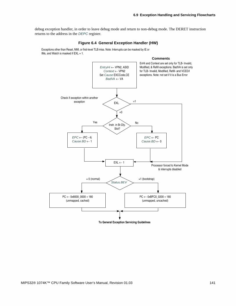
6.9 Exception Handling and Servicing Flowcharts
MIPS32® 1074K™ CPU Family Software User’s Manual, Revision 01.03 141
debug exception handler, in order to leave debug mode and return to non-debug mode. The DERET instructionreturns to the address in the DEPC register.
Figure 6.4 General Exception Handler (HW)
To General Exception Servicing Guidelines
=1 (bootstrap)= 0 (normal)Status.BEV
Comments
PC ← 0x8000_0000 + 180(unmapped, cached)
PC ← 0xBFC0_0200 + 180(unmapped, uncached)
EXL ← 1
EPC ← (PC - 4)Cause.BD ← 1
EPC ← PCCause.BD ← 0
Instr. in Br.Dly.Slot?
Yes
Processor forced to Kernel Mode& interrupts disabled
=0
=1Check if exception within another
exception EXL
EnHi and Context are set only for TLB- Invalid,Modified, & Refill exceptions. BadVA is set onlyfor TLB- Invalid, Modified, Refill- and VCED/Iexceptions. Note: not set if it is a Bus Error
EntryHi ← VPN2, ASIDContext ← VPN2
Set Cause EXCCode,CEBadVA ← VA
Exceptions other than Reset, NMI, or first-level TLB miss. Note: Interrupts can be masked by IE orIMs, and Watch is masked if EXL = 1.
No

Exceptions and Interrupts in the 1074K™ CPU
142 MIPS32® 1074K™ CPU Family Software User’s Manual, Revision 01.03
Figure 6.5 General Exception Servicing Guidelines (SW)
ERET
MTC0 -EPC,STATUS
EXL = 1
Service Code
* ERET is not allowed in the branch delay slot of another JumpInstruction* Processor does not execute the instruction which is in the ERET’sbranch delay slot* PC ← EPC; EXL ← 0* LLbit ← 0
Check Cause value & Jump to appropriateService Code
* After EXL=0, all exceptions allowed (exceptinterrupt if masked by IE)
(Optional - only to enable Interrupts while keeping Kernel Mode)
MTC0 -Set Status bits:
UM←0, EXL←0, IE←1
MFC0 -Context, EPC, Status, Cause
* Unmapped vector so TLBMod, TLBInv, or TLB Refill exceptionsnot possible* EXL=1 so Watch and Interrupt exceptions disabled* OS/System to avoid all other exceptions* Only Reset, Soft Reset, NMI exceptions possible.
Comments

6.9 Exception Handling and Servicing Flowcharts
MIPS32® 1074K™ CPU Family Software User’s Manual, Revision 01.03 143
Figure 6.6 TLB Miss Exception Handler (HW)
To TLB Exception Servicing Guidelines
Vec. Off. = 0x180
EPC ← (PC - 4)Cause.BD ← 1
EPC ← PCCause.BD ← 0
Vec. Off. = 0x000
EXL ← 1
Points to General Exception
Processor forced to Kernel Mode &interrupts disabled
=0
=1 (bootstrap)= 0 (normal)
PC ← 0x8000_0000 + Vec.Off.(unmapped.cached)
PC ← 0xBFC0_0200 + Vec.Off. (unmapped.uncached)
Status.BEV
Check if exception within anotherexception=1=1
=0
EXL EXL
EntryHi ← VPN2, ASIDContext ← VPN2
Set Cause EXCCode,CEBadVA ← VA
Instr. in Br.Dly.Slot?
NoYes

Exceptions and Interrupts in the 1074K™ CPU
144 MIPS32® 1074K™ CPU Family Software User’s Manual, Revision 01.03
Figure 6.7 TLB Exception Servicing Guidelines (SW)
Comments
ERET
Service Code
MFC0 -CONTEXT
* Unmapped vector so TLBMod, TLBInv, or TLB Refill exceptionsnot possible* EXL=1 so Watch, Interrupt exceptions disabled* OS/System to avoid all other exceptions* Only Reset, Soft Reset, NMI exceptions possible.
* Load the mapping of the virtual address in Context Reg. Move itto EntryLo and write into the TLB* There could be a TLB miss again during the mapping of the dataor instruction address. The processor will jump to the generalexception vector since the EXL is 1. (Option to complete the firstlevel refill in the general exception handler or ERET to the originalinstruction and take the exception again)
* ERET is not allowed in the branch delay slot of another JumpInstruction* Processor does not execute the instruction which is in the ERET’sbranch delay slot* PC ← EPC; EXL ← 0* LLbit ← 0

6.9 Exception Handling and Servicing Flowcharts
MIPS32® 1074K™ CPU Family Software User’s Manual, Revision 01.03 145
Figure 6.8 Reset and NMI Exception Handling and Servicing Guidelines
Status:BEV ← 1TS ← 0SR ← 0NMI ← 1ERL ← 1
(Optional)
Reset Service Code
NMI Service Code
ERET
=0
=1
PC ← 0xBFC0_0000
ErrorEPC ← PC
Random ← TLBENTRIES - 1Wired ← 0Config ← Reset stateStatus:
RP ← 0BEV ← 1TS ← 0SR ← 0NMI ← 0ERL ← 1
WatchLo:I, R,W ← 0
Reset Exception
NMI ExceptionR
eset
, Sof
t Res
et &
NM
I Exc
eptio
n H
andl
ing
(HW
)R
eset
, Sof
t Res
et &
NM
I Ser
vici
ngG
uide
lines
(SW
)

Exceptions and Interrupts in the 1074K™ CPU
146 MIPS32® 1074K™ CPU Family Software User’s Manual, Revision 01.03

Chapter 7
MIPS32® 1074K™ CPU Family Software User’s Manual, Revision 01.03 147
CP0 Registers of the 1074K™ CPU
The System Control Coprocessor (CP0) provides the register interface to the 1074K CPU and supports memory man-agement, address translation, exception handling, and other privileged operations. Each CP0 register has a uniquenumber that identifies it, referred to as its register number. CP0 register numbers are denoted by n.s, where n is theregister number (between 0-31) and s is the "select" field (0-7). If the select field is omitted, it is zero. A select fieldof x denotes all eight potential select numbers.
This chapter contains the following sections:
• Section 7.1 “CP0 Register Summary”
• Section 7.2 “CP0 Register Descriptions”
The CP0 EJTAG registers are described in Chapter 11, “EJTAG Debug Support in the 1074K™ CPU."
7.1 CP0 Register Summary
The CP0 registers are described in three tables. Table 7.1 lists the registers in alphabetic order, Table 7.2 lists the reg-isters in numerical order, and Table 7.3 groups the registers according to their function. The CP0 registers aredescribed individually in Section 7.2, "CP0 Register Descriptions."
Table 7.1 CP0 Registers in Alphabetical Order
Name Number Name Number Name Number Name Number
BadVAddr 8.0 DDataLo 28.3 IDataLo 28.1 SRSMap 12.3
CacheErr 27.0 Debug 23.0 Index 0.0 Status 12.0
Cause 13.0 DEPC 24.0 IntCtl 12.1 TraceControl 23.1
CDMMBase 15.2 DESAVE 31.0 ITagHi 29.0 TraceControl2 23.2
CMGCRBase 15.3 DTagHi 29.2 ITagLo 28.0 TraceControl3 24.2
Compare 11.0 DTagLo 28.2 L23DataHi 29.5 TraceIPBC 23.4
Config 16.0 EBase 15.1 L23DataLo 28.5 TraceDPBC 23.5
Config1-2 16.1-2 EntryHi 10.0 L23TagLo 28.4 UserLocal 4.2
Config3 16.3 EntryLo0-1 2.03.0
PageMask 5.0 UserTraceData1 23.3
Config6 16.6 EPC 14.0 PerfCnt0-3 25.125.325.525.7
UserTraceData2 24.3

CP0 Registers of the 1074K™ CPU
148 MIPS32® 1074K™ CPU Family Software User’s Manual, Revision 01.03
Config7 16.7 ErrCtl 26.0 PerfCtl0-3 25.025.225.425.6
WatchHi0-3 19.0-3
Context 4.0 ErrorEPC 30.0 PRId 15.0 WatchLo0-3 18.0-3
ContextConfig 4.1 HWREna 7.0 Random 1.0 Wired 6.0
Count 9.0 IDataHi 29.1 SRSCtl 12.2
Table 7.2 CP0 Registers in Numerical Order
Number Register Description Page
0.0 Index Index into the TLB array 7.2.1, p.153
1.0 Random Randomly generated index into the TLB array 7.2.2, p.154
2.03.0
EntryLo0-1 Output (physical) side of TLB entry (even-/odd-numbered virtualpages)
7.2.3, p.154
4.0 Context Mixture of pre-programmed and BadVAddr bits which can act as anOS page table pointer.
7.2.4, p.156
4.1 ContextConfig Defines the bits of the Context register into which the high order bitsof the virtual address causing a TLB exception will be written.
7.2.5, p.157
4.2 UserLocal Kernel-writable but user-readable software-defined thread ID 7.2.6, p.158
5.0 PageMask Control for variable page size in TLB entries 7.2.7, p.159
6.0 Wired Controls the number of fixed ("wired") TLB entries 7.2.8, p.160
7.0 HWREna Bitmask limiting user-mode access to rdhwr registers 7.2.9, p.160
8.0 BadVAddr Address causing the last TLB-related exception 7.2.10, p.162
9.0 Count Free-running counter at half pipeline speed 7.11, p.162
10.0 EntryHi High-order portion of the TLB entry 7.2.12, p.163
11.0 Compare Timer interrupt control 7.2.13, p.164
12.0 Status Processor status and control 7.2.14, p.164
12.1 IntCtl Setup for interrupt vector and interrupt priority features. 7.2.15, p.170
12.2 SRSCtl Shadow register set selectors 7.2.16, p.171
12.3 SRSMap Shadow set choice for each interrupt level in VI mode 7.2.17, p.173
13.0 Cause Cause of last general exception 7.2.18, p.174
14.0 EPC Restart address from exception 7.2.19, p.178
15.0 PRId Processor identification and revision 7.2.20, p.179
15.1 EBase Exception entry point base address and CPU/VPE ID 7.2.21, p.180
15.2 CDMMBase 36-bit physical base address for the Common Device Memory Mapfacility
7.2.22, p.181
15.3 CMGCRBase Coherency Manager Global Configuration Register Base Address 7.2.23, p.182
Table 7.1 CP0 Registers in Alphabetical Order (Continued)
Name Number Name Number Name Number Name Number

7.1 CP0 Register Summary
MIPS32® 1074K™ CPU Family Software User’s Manual, Revision 01.03 149
16.0 Config Legacy configuration register 7.2.24, p.182
16.1-2 Config1-2 MIPS32/64 configuration registers (caches etc) 7.2.25, p.184
16.3 Config3 Configuration register showing ASEs etc 7.2.26, p.186
16.6 Config6 Additional information about the presence of optional extensions to thebase MIPS32 architecture
7.2.27, p.187
16.7 Config7 CPU-specific configuration 7.2.28, p.190
18.0-3 WatchLo0-3 Watchpoint address and qualifiers 7.2.29, p.193
19.0-3 WatchHi0-3 Watchpoint control/status 7.2.30, p.193
23.0 Debug EJTAG Debug status/control register 7.2.31, p.194
23.1 TraceControl EJTAG Trace Control register 7.2.32, p.198
23.2 TraceControl2 EJTAG Trace Control2 register 7.2.33, p.200
23.3 UserTraceData1 EJTAG User Trace Data1 register 7.2.34, p.202
23.4 TraceIBPC EJTAG Trace Instruction breakpoint control register 7.2.35, p.203
23.5 TraceDBPC EJTAG Trace Data breakpoint control register 7.2.36, p.204
24.0 DEPC Restart address from last EJTAG debug exception 7.2.37, p.205
24.2 TraceControl3 EJTAG Trace Control3 register 7.2.38, p.206
24.3 UserTraceData2 EJTAG User Trace Data2 register 7.2.34, p.202
25.025.225.425.6
PerfCtl0-3 Performance counter control 7.2.39, p.207
25.125.325.525.7
PerfCnt0-3 Performance counters 7.2.40, p.212
26.0 ErrCtl Software parity control and test modes for cache RAM arrays 7.2.41, p.212
27.0 CacheErr Cache parity exception status 7.2.42, p.213
28.0 ITagLo Read/write interface for I-cache tag cacheops 7.2.43, p.215
28.1 IDataLo Low-order data read/write interface for I-cache special cacheops 7.2.44, p.217
28.2 DTagLo Read/write interface for load/store tag cacheops 7.2.45, p.217
28.3 DDataLo Low-order data read/write interface for D-cache 7.2.46, p.223
28.4 L23TagLo Level 2/3 cache Tag information 7.2.47, p.223
28.5 L23DataLo Low-order data read/write interface for Level 2/3 cache 7.2.48, p.223
29.0 ITagHi I-cache predecode bits 7.2.49, p.224
29.1 IDataHi High-order data read/write interface for I-cache special cacheops 7.2.50, p.224
29.2 DTagHi D-cache virtual index (including ASID) 7.2.51, p.224
29.5 L23DataHi High-order data read/write interface for Level 2/3 cache 7.2.52, p.225
30.0 ErrorEPC Restart location from a reset or a cache error exception 7.2.53, p.225
31.0 DESAVE Scratch read/write register for EJTAG debug exception handler 7.2.54, p.226
Table 7.2 CP0 Registers in Numerical Order (Continued)
Number Register Description Page

CP0 Registers of the 1074K™ CPU
150 MIPS32® 1074K™ CPU Family Software User’s Manual, Revision 01.03

7.1 CP0 Register Summary
MIPS32® 1074K™ CPU Family Software User’s Manual, Revision 01.03 151
Note that after a CP0 register has been updated, there is a hazard period of zero or more instructions from the updateinstruction (mtc0) until the update has taken effect in the CPU. There is no automatic handling of hazard by the hard-ware in the 1074K CPU. Release 2 requires that an ehb (Execution Hazard Barrier) instruction be placed betweenthese two instructions when they address the same CPO register. For more information about the MIPS32® Release 2Architecture guidelines on hazard barriers, refer to Section 2.3, "Hazards."
Table 7.3 CP0 Registers Grouped by Function
Basic modes Status 12.0
TLBManagement
BadVAddr 8.0
EJTAG Debug
DEPC 24.0
OS/userlandthread ID
UserLocal 4.2 Context 4.0 DESAVE 31.0
ExceptionControl
Cause 13.0 ContextConfig
4.1 Debug 23.0
EPC 14.0 EntryHi 10.0
PDtrace
TraceControl 23.1
Timer
Compare 11.0 EntryLo0-1 2.03.0
TraceControl2 23.2
Count 9.0 Index 0.0 TraceControl3 24.2
CPUConfiguration
Config 16.0 PageMask 5.0 TraceIPBC 23.4
Config1-2 16.1-2 Random 1.0 TraceIDBC 23.5
Config3 16.3 Wired 6.0 UserTraceData1 23.3
Config6 16.6
CacheManagement
DDataLo 28.3 UserTraceData2 24.3
Config7 16.7 DTagHi 29.2
Profiling
PerfCnt0-3 25.125.325.525.7
EBase 15.1 DTagLo 28.2 PerfCtl0-3 25.025.225.425.6
CDMMBase 15.2 ErrCtl 28.2 PerfCnt0-3 25.125.325.525.7
CMGCRBase 15.3
IntCtl 12.1 ErrorEPC 26.0Debug/Analysis
WatchHi0-3 19.0-3
PRId 15.0 IDataHi 29.1 WatchLo0-3 18.0-3
SRSCtl 12.2 IDataLo 28.1 Control rdhwrAccess HWREna 7.0
SRSMap 12.3 ITagHi 29.0 Parity/ECCcontrol CacheErr 27.0
ITagLo 28.0
L23DataHi 29.5
L23TagLo 28.4

CP0 Registers of the 1074K™ CPU
152 MIPS32® 1074K™ CPU Family Software User’s Manual, Revision 01.03
7.2 CP0 Register Descriptions
This section contains descriptions of each CP0 register. The registers are listed in numerical order, first by registernumber, then by select field number.
R/W Access Types
For each register described below, field descriptions include the read/write access properties of the field and the resetstate of the field. The read/write access properties are described in Table 7.4.
Table 7.4 CP0 Register Field R/W Access Types
Notation Hardware Interpretation Software Interpretation
R/W A field in which all bits are readable and writable by software and potentially by hardware.Hardware updates of this field are visible by software reads. Software updates of this field are visible by hardwarereads.If the reset state of this field is “Undefined”, either software or hardware must initialize the value before the firstread will return a predictable value. This should not be confused with the formal definition of UNDEFINEDbehavior.
SO Software Only. A field that is read and written by software but has no hardware effect. An example is theDESAVE register.
R A field that is either static or is updated only by hard-ware.If the Reset State of this field is either “0” or “Preset”,hardware initializes this field to zero or to the appropri-ate state, respectively, on powerup.If the Reset State of this field is “Undefined”, hardwareupdates this field only under those conditions specifiedin the description of the field.
A field to which the value written by software isignored by hardware. Software may write any value tothis field without affecting hardware behavior. Softwarereads of this field return the last value updated by hard-ware.If the Reset State of this field is “Undefined,” softwarereads of this field result in an UNPREDICTABLEvalue except after a hardware update done under theconditions specified in the description of the field.
W A field that can be written by software but which cannot be read by software.Software reads of this field will return an UNDEFINED value.
W0 Hardware can write 1’s or 0’s to this field. Software writes will only cause the bit to be cleared.Software can never set this bit. An example is the NMIbit field in the Status register.
W1C Hardware can write 1’s or 0’s to this field. Software should write “1” to this bit to clear it. Anexample is the I, R, and W bit fields in the WatchHi0-3register.
0 A field that hardware does not update, and for whichhardware can assume a zero value.
A field to which the value written by software must bezero. Software writes of non-zero values to this fieldmay result in UNDEFINED behavior of the hardware.Software reads of this field return zero as long as allprevious software writes are zero.If the Reset State of this field is “Undefined”, softwaremust write this field with zero before it is guaranteed toread as zero.
U A field that is not read or written by hardware. Software writes to this field will be ignored. Softwarereads of this field will return an UNDEFINED value.

7.2 CP0 Register Descriptions
MIPS32® 1074K™ CPU Family Software User’s Manual, Revision 01.03 153
Color Coding of Register Descriptions
The color codes used in the register descriptions to indicate the access types are summarized in Figure 7.1. A fieldwith two access types (for example, R/W0) is uncolored,
Figure 7.1 Register Format Color Coding of Access Field Types
Power-up State of CP0 Registers
The traditions of the MIPS architecture regard it as software’s job to initialize CP0 registers. As a rule, only fieldswhere a wrong setting could prevent the CPU from booting are specified to be brought to a particular state by reset;other fields—perhaps other fields in the same register—are undefined. This manual documents where a field has aforced-from-reset value; conversely, when no reset-time value is documented, that means the register comes up in anundefined state.
To ensure robust programs, you should initialize all CP0 register fields, except those in which a random value isknown to be harmless.
A Note on Unused Fields in CP0 Registers
Unused fields in registers are marked either with the digit 0, an "X", or occasionally a "U". A field marked zero isexpected to read zero; a field marked "U" is expected to read back whatever you last wrote to it; and if the field ismarked "X", the value is unpredictable.
But again, for robustness, you should write unused fields either to a value you previously read from the same field or(if no such value is available) to zero.
7.2.1 Index (CP0 Register 0, Select 0): Index into TLB array
Index is used as the TLB index when reading or writing the TLB with tlbr/tlbw respectively. It is also set by aTLB probe (tlbp) instruction to return the location of an address match in the TLB.
The operation of the processor is UNDEFINED if a value greater than or equal to the number of TLB entries is writ-ten to the Index register.
This register is only valid when the TLB is implemented; it is reserved if the FM is implemented.
Figure 7.2 Index Register Format
31 5 0
R/W SO RWRITE HAS UNUSUALEFFECT (W, WO, W1C)
0 U
31 30 6 5 0
P 0 Index
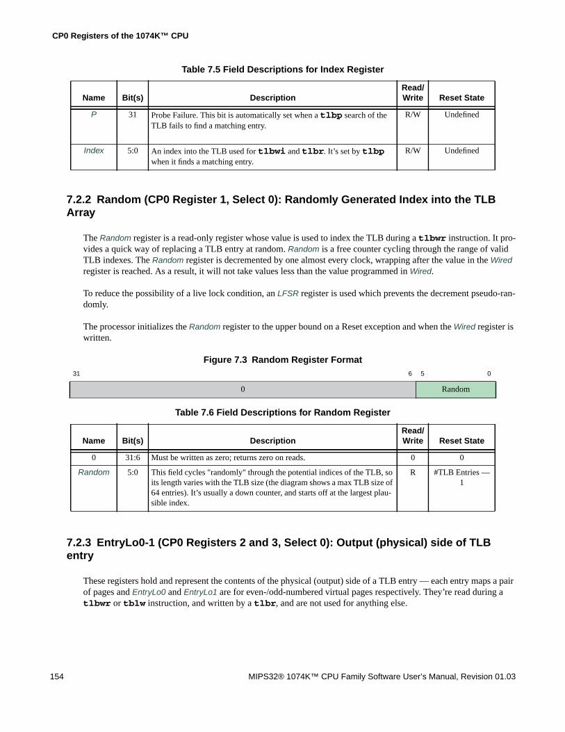
CP0 Registers of the 1074K™ CPU
154 MIPS32® 1074K™ CPU Family Software User’s Manual, Revision 01.03
7.2.2 Random (CP0 Register 1, Select 0): Randomly Generated Index into the TLBArray
The Random register is a read-only register whose value is used to index the TLB during a tlbwr instruction. It pro-vides a quick way of replacing a TLB entry at random. Random is a free counter cycling through the range of validTLB indexes. The Random register is decremented by one almost every clock, wrapping after the value in the Wiredregister is reached. As a result, it will not take values less than the value programmed in Wired.
To reduce the possibility of a live lock condition, an LFSR register is used which prevents the decrement pseudo-ran-domly.
The processor initializes the Random register to the upper bound on a Reset exception and when the Wired register iswritten.
Figure 7.3 Random Register Format
7.2.3 EntryLo0-1 (CP0 Registers 2 and 3, Select 0): Output (physical) side of TLBentry
These registers hold and represent the contents of the physical (output) side of a TLB entry — each entry maps a pairof pages and EntryLo0 and EntryLo1 are for even-/odd-numbered virtual pages respectively. They’re read during atlbwr or tblw instruction, and written by a tlbr, and are not used for anything else.
Table 7.5 Field Descriptions for Index Register
Name Bit(s) DescriptionRead/Write Reset State
P 31 Probe Failure. This bit is automatically set when a tlbp search of theTLB fails to find a matching entry.
R/W Undefined
Index 5:0 An index into the TLB used for tlbwi and tlbr. It’s set by tlbpwhen it finds a matching entry.
R/W Undefined
31 6 5 0
0 Random
Table 7.6 Field Descriptions for Random Register
Name Bit(s) DescriptionRead/Write Reset State
0 31:6 Must be written as zero; returns zero on reads. 0 0
Random 5:0 This field cycles "randomly" through the potential indices of the TLB, soits length varies with the TLB size (the diagram shows a max TLB size of64 entries). It’s usually a down counter, and starts off at the largest plau-sible index.
R #TLB Entries —1

7.2 CP0 Register Descriptions
MIPS32® 1074K™ CPU Family Software User’s Manual, Revision 01.03 155
Figure 7.4 EntryLo0, EntryLo1 Register Format
Table 7.8 Cache Coherency Attributes encoding of C field of EntryLo0-1 and K0 field of Config Register
31 26 25 6 5 3 2 1 0
0 PFN C D V G
Table 7.7 Field Descriptions for EntryLo0-1 Register
Name Bit(s) DescriptionRead/Write Reset State
PFN 25:6 The "physical frame number" — traditional OS name for the high-orderbits of the physical address. 20 bits of PFN together with 12 bits of in-page address make up a 32-bit physical address. The MIPS32® Architec-ture permits the PFN to be as large as 24 bits, but the 1074K CPU has a32-bit physical address bus.
R/W Undefined
C 5:3 Coherency attribute of the page. See Table 7.8. R/W Undefined
D 2 The "dirty" flag. Indicates that the page has been written, and/or is writ-able. If this bit is a one, then stores to the page are permitted. If this bit isa zero, then stores to the page cause a TLB Modified exception.Software can use this bit to track pages that have been written to; whenyou first map a page, you leave this bit clear, and then the first writecauses an exception which you note somewhere in the OS’ memory man-agement tables (and, of course, remember to set the bit).
R/W Undefined
V 1 The “valid” flag. Indicates that the TLB entry, and thus the virtual pagemapping are valid. If this bit is a one, then accesses to the page are per-mitted. If this bit is a zero, then accesses to the page cause a TLB Invalidexception.This bit can be used to make just one of a pair of pages valid.
R/W Undefined
G 0 The “global” bit. On a TLB write, the logical AND of the G bits in boththe EntryLo0 and EntryLo1 registers become the G bit in the TLB entry.If the TLB entry G bit is a one, then the ASID comparisons are ignoredduring TLB matches. On a read from a TLB entry, the G bits of bothEntryLo0 and EntryLo1 reflect the state of the TLB G bit.
R/W Undefined
C[5:3]K0[2:0] Cache Coherency Attribute
0 Reserved
1 Reserved
2 uncached
3 Cacheable, noncoherent, write-back, write allocate
4 Cacheable, write-back, write-allocate, coherent, read missesrequest Exclusive
5 Cacheable, write-back, write-allocate, coherent, read missesrequest Shared
6 Reserved
7 Uncached Accelerated

CP0 Registers of the 1074K™ CPU
156 MIPS32® 1074K™ CPU Family Software User’s Manual, Revision 01.03
7.2.4 Context (CP0 Register 4, Select 0): Mixture of Pre-programmed and BadVAddrBits which can act as an OS Page Table Pointer.
The Context register is a read/write register containing a pointer to an entry in the page table entry (PTE) array. Thisarray is an operating system data structure that stores virtual-to-physical translations. During a TLB miss, the operat-ing system loads the TLB with the missing translation from the PTE array.The Context register duplicates some of theinformation provided in the BadVAddr register.
The BadVPN2 field of the Context register is not defined after an address error exception, and this field may be modi-fied by hardware during the address error exception sequence.
If Config3CTXTC =1, the pointer implemented by the Context register can point to any power-of-two-sized PTE struc-ture within memory. This allows the TLB refill handler to use the pointer without additional shifting and maskingsteps. Depending on the value in the ContextConfig register, it may point to an 8-byte pair of 32-bit PTEs within a sin-gle-level page table scheme, or to a first level page directory entry in a two-level lookup scheme.
A TLB exception (Refill, Invalid, or Modified) causes bits VA31:32-X+Y to be written to a variable range of bits “(X-1):Y” of the Context register, where this range corresponds to the contiguous range of set bits in the ContextConfigregister. Bits 31:X are R/W to software, and are unaffected by the exception. Bits Y-1:0 will always read as 0. If X =23 and Y = 4, i.e. bits 22:4 are set in ContextConfig, the behavior is identical to the standard MIPS32 Context register(bits 22:4 are filled with VA31:13). Although the fields have been made variable in size and interpretation, the MIPS32nomenclature is retained. Bits 31:X are referred to as the PTEBase field, and bits X-1:Y are referred to as BadVPN2.When Config3CTXTC =0, X = 23, Y = 4.
The value of the Context register is UNPREDICTABLE following a modification of the contents of theContextConfig register.
Figure 7-5 shows the format of the Context Register; Table 7.9 describes the Context register fields.
Figure 7-5 Context Register Format31 X X-1 Y Y-1 0
PTEBase BadVPN2 0
Table 7.9 Context Register Field Descriptions
Fields
DescriptionRead /Write
ResetStateName Bits
PTEBase Variable, 31:X whereX in {31..0}.May be null.If Config3CTXTC =0,X = 23
This field is for use by the operating systemand is normally written with a value thatallows the operating system to use theContext Register as a pointer to an array ofdata structures in memory corresponding tothe address region that contains the virtualaddress which caused the exception.
R/W Undefined

7.2 CP0 Register Descriptions
MIPS32® 1074K™ CPU Family Software User’s Manual, Revision 01.03 157
7.2.5 ContextConfig Register (CP0 Register 4, Select 1)
The ContextConfig register defines the bits of the Context register into which the high order bits of the virtual addresscausing a TLB exception will be written, and how many bits of that virtual address will be extracted. Bits above theselected of the Context register are R/W to software and serve as the PTEBase field. Bits below the selected field ofthe Context register will read as zeroes.
The field to contain the virtual address index is defined by a single block of contiguous non-zero bits within theContextConfig register’s VirtualIndex field. Any zero bits to the right of the least significant one bit cause the corre-sponding Context register bits to read as zero. Any zero bits to the left of the most significant one bit cause the corre-sponding Context register bits to be R/W to software and unaffected by TLB exceptions.
A value of all ones in the ContextConfig register means that the full 32 bits of the faulting virtual address will be cop-ied into the context register, making it duplicate the BadVAddr register. A value of all zeroes means that the full 32bits of the Context register are R/W for software and unaffected by TLB exceptions.
The ContextConfig register is optional and its existence is denoted by the Config3CTXTC or Config3SM register fields.
Figure 7.6 shows the formats of the ContextConfig Register; Table 7.10 describes the ContextConfig register fields.
Figure 7.6 ContextConfig Register Format
BadVPN2 Variable, (X-1):YwhereX in {32..1} andY in {31..0}.May be null.If Config3CTXTC =0,X = 23, Y = 4
This field is written by hardware on a TLBexception. It contains bits VA31:32-X+Y of thevirtual address that caused the exception.
R Undefined
0 Variable, (Y-1):0whereY in {31:1}.May be null.If Config3CTXTC =0,Y = 4
Must be written as zero; returns zero on read. 0 0
31 0
VirtualIndex
Table 7.9 Context Register Field Descriptions
Fields
DescriptionRead /Write
ResetStateName Bits
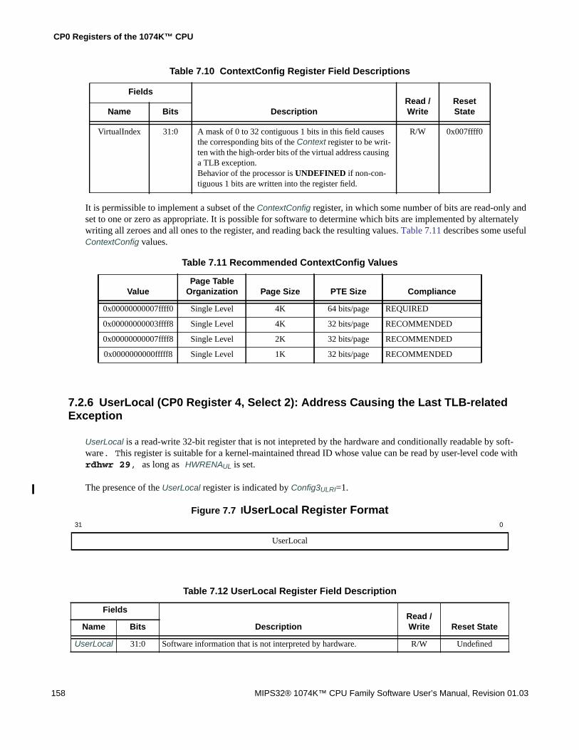
CP0 Registers of the 1074K™ CPU
158 MIPS32® 1074K™ CPU Family Software User’s Manual, Revision 01.03
It is permissible to implement a subset of the ContextConfig register, in which some number of bits are read-only andset to one or zero as appropriate. It is possible for software to determine which bits are implemented by alternatelywriting all zeroes and all ones to the register, and reading back the resulting values. Table 7.11 describes some usefulContextConfig values.
7.2.6 UserLocal (CP0 Register 4, Select 2): Address Causing the Last TLB-relatedException
UserLocal is a read-write 32-bit register that is not intepreted by the hardware and conditionally readable by soft-ware. This register is suitable for a kernel-maintained thread ID whose value can be read by user-level code withrdhwr 29, as long as HWRENAUL is set.
The presence of the UserLocal register is indicated by Config3ULRI=1.
Figure 7.7 IUserLocal Register Format
Table 7.10 ContextConfig Register Field Descriptions
Fields
DescriptionRead /Write
ResetStateName Bits
VirtualIndex 31:0 A mask of 0 to 32 contiguous 1 bits in this field causesthe corresponding bits of the Context register to be writ-ten with the high-order bits of the virtual address causinga TLB exception.Behavior of the processor is UNDEFINED if non-con-tiguous 1 bits are written into the register field.
R/W 0x007ffff0
Table 7.11 Recommended ContextConfig Values
ValuePage Table
Organization Page Size PTE Size Compliance
0x00000000007ffff0 Single Level 4K 64 bits/page REQUIRED
0x00000000003ffff8 Single Level 4K 32 bits/page RECOMMENDED
0x00000000007ffff8 Single Level 2K 32 bits/page RECOMMENDED
0x0000000000fffff8 Single Level 1K 32 bits/page RECOMMENDED
31 0
UserLocal
Table 7.12 UserLocal Register Field Description
Fields
DescriptionRead /Write Reset StateName Bits
UserLocal 31:0 Software information that is not interpreted by hardware. R/W Undefined

7.2 CP0 Register Descriptions
MIPS32® 1074K™ CPU Family Software User’s Manual, Revision 01.03 159
7.2.7 PageMask (CP0 Register 5, Select 0): Control for Variable Page Size in TLBEntries
Every TLB entry has an independent virtual-address mask that allows it to ignore some address bits when deciding tomatch. By selectively ignoring lower page addresses, the entry can be made to match all the addresses in a "page"larger than 4KB.
Software can determine which page sizes are supported by writing all ones to the PageMask register, then reading thevalue back. If a pair of bits reads back as ones, the processor implements that page size. The operation of the proces-sor is UNDEFINED if software loads the Mask field with a value other than one of those listed in Table 7.13, even ifthe hardware returns a different value on read. Hardware may depend on this requirement in implementing hardwarestructures.
Figure 7.8 PageMask Register Format31 29 28 13 12 0
0 Mask 0
Table 7.13 Field Descriptions for PageMask Register
Name Bit(s) DescriptionRead/Write Reset State
0 31:29,12:0
Ignored on write; returns zero on read. R 0
Mask 28:13 Acts as a kind of backward mask, in that a 1 bit means "don’t comparethis address bit when matching this address". However, only a restrictedrange of PageMask values are legal (i.e., with "1"s filling thePageMaskMask field from low bits upward, two at a time):
Note that the uTLBs handle only 4Kbyte and 1Mbyte page sizes; otherpage sizes are down-converted to 4Kbyte or 1Mbyte as they are refer-enced. For other page sizes, this may cause an unexpectedly high rate ofuTLB misses, which could lead to a noticeable performance loss.
R/W Undefined
PageMaskValue
Size of Each OutputPage
0x0000.0000 4 Kbytes
0x0000.6000 16 Kbytes
0x0001.E000 64 Kbytes
0x0007.E000 256 Kbytes
0x001F.E000 1 Mbyte
0x007F.E000 4 Mbytes
0x01FF.E000 16 Mbytes
0x07FF.E000 64 Mbytes
0x1FFF.E000 256 Mbytes
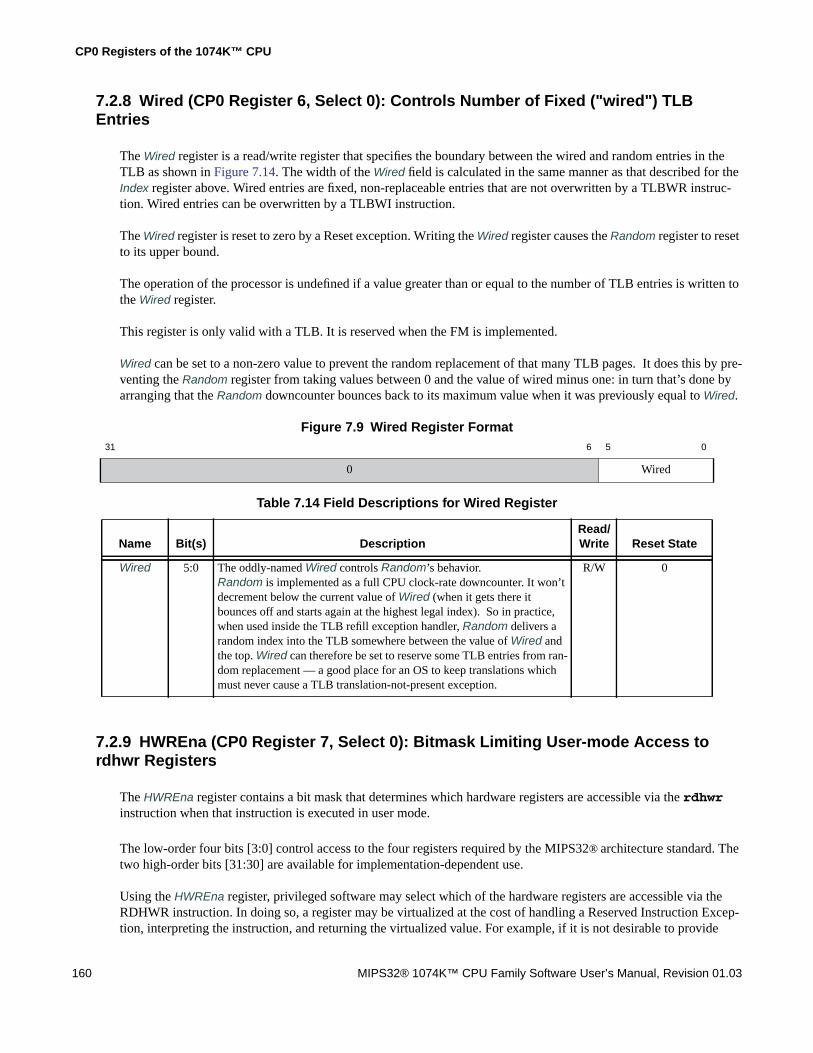
CP0 Registers of the 1074K™ CPU
160 MIPS32® 1074K™ CPU Family Software User’s Manual, Revision 01.03
7.2.8 Wired (CP0 Register 6, Select 0): Controls Number of Fixed ("wired") TLBEntries
The Wired register is a read/write register that specifies the boundary between the wired and random entries in theTLB as shown in Figure 7.14. The width of the Wired field is calculated in the same manner as that described for theIndex register above. Wired entries are fixed, non-replaceable entries that are not overwritten by a TLBWR instruc-tion. Wired entries can be overwritten by a TLBWI instruction.
The Wired register is reset to zero by a Reset exception. Writing the Wired register causes the Random register to resetto its upper bound.
The operation of the processor is undefined if a value greater than or equal to the number of TLB entries is written tothe Wired register.
This register is only valid with a TLB. It is reserved when the FM is implemented.
Wired can be set to a non-zero value to prevent the random replacement of that many TLB pages. It does this by pre-venting the Random register from taking values between 0 and the value of wired minus one: in turn that’s done byarranging that the Random downcounter bounces back to its maximum value when it was previously equal to Wired.
Figure 7.9 Wired Register Format
7.2.9 HWREna (CP0 Register 7, Select 0): Bitmask Limiting User-mode Access tordhwr Registers
The HWREna register contains a bit mask that determines which hardware registers are accessible via the rdhwrinstruction when that instruction is executed in user mode.
The low-order four bits [3:0] control access to the four registers required by the MIPS32® architecture standard. Thetwo high-order bits [31:30] are available for implementation-dependent use.
Using the HWREna register, privileged software may select which of the hardware registers are accessible via theRDHWR instruction. In doing so, a register may be virtualized at the cost of handling a Reserved Instruction Excep-tion, interpreting the instruction, and returning the virtualized value. For example, if it is not desirable to provide
31 6 5 0
0 Wired
Table 7.14 Field Descriptions for Wired Register
Name Bit(s) DescriptionRead/Write Reset State
Wired 5:0 The oddly-named Wired controls Random’s behavior.Random is implemented as a full CPU clock-rate downcounter. It won’tdecrement below the current value of Wired (when it gets there itbounces off and starts again at the highest legal index). So in practice,when used inside the TLB refill exception handler, Random delivers arandom index into the TLB somewhere between the value of Wired andthe top. Wired can therefore be set to reserve some TLB entries from ran-dom replacement — a good place for an OS to keep translations whichmust never cause a TLB translation-not-present exception.
R/W 0

7.2 CP0 Register Descriptions
MIPS32® 1074K™ CPU Family Software User’s Manual, Revision 01.03 161
direct access to the Count register, access to that register may be individually disabled and the return value can be vir-tualized by the operating system.
Software may determine which registers are implemented by writing all ones to the HWREna register, then readingthe value back. If a bit reads back as a one, the processor implements that hardware register.
Figure 7.10 HWREna Register Format31 30 29 28 4 3 2 1 0
Impl UL 0 CCRes CC SYNCI_Step CPUNum
Table 7.15 Field Descriptions for HWREna Register
Name Bit(s) DescriptionRead/Write Reset State
Impl 31:30 These bits control access to implementation-dependent hardware regis-ters. These registers are not currently implemented in any 1074K familyprocessor. Attempts to access these bits results in a Reserved InstructionException.
R 0
UL 29 User Local Register. This register provides read access to the coprocessor0 UserLocal register. Set this bit to 1 to permit user programs to obtainthe value of the UserLocal CP0 register using rdhwr 29.
R/W 0
CCRes 3 Resolution of the CC register. This value denotes the number of cyclesbetween update of the register. For example:
Set this bit to 1 so a user-mode rdhwr 3 can read the CCRes value. TheCCRes register will read a value of 2 when the Count register runs athalf the pipeline speed (as it always does in 1074K family CPUs).
R/W 0
CC 2 High-resolution Cycle Counter. This register provides read access to thecoprocessor 0 Count Register. Set this bit to 1 so a user-moderdhwr 2 can read out the value of the Count register.
R/W 0
SYNCI_Step 1 Address step size to be used with the SYNCI instruction. See that instruc-tion’s description for the use of this value. In the typical implementation,this value should be zero if there are no caches in the system that must besynchronized (either because there are no caches, or because the instruc-tion cache tracks writes to the data cache). In other cases, the return valueshould be the smallest line size of the caches that must be synchronized.For the 1074K 1074k, the SYNCI_Step value is 32 since the line size is32 bytes.Set this bit to 1 so a user-mode rdhwr 1 can read the cache line size(actually, the smaller of the L1 I-cache line size and D-cache line size).That line size determines the step between successive uses of the synciinstruction, which does the cache manipulation necessary to ensure thatthe CPU can correctly execute instructions which you just wrote.
R/W 0
CCRes Value Meaning
1 CC register increments every cycle
2 CC register increments every second cycle
3 CC register increments every third cycle
etc.
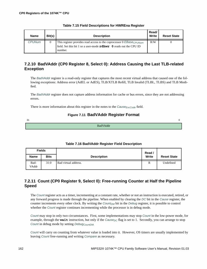
CP0 Registers of the 1074K™ CPU
162 MIPS32® 1074K™ CPU Family Software User’s Manual, Revision 01.03
7.2.10 BadVAddr (CP0 Register 8, Select 0): Address Causing the Last TLB-relatedException
The BadVAddr register is a read-only register that captures the most recent virtual address that caused one of the fol-lowing exceptions: Address error (AdEL or AdES), TLB/XTLB Refill, TLB Invalid (TLBL, TLBS) and TLB Modi-fied.
The BadVAddr register does not capture address information for cache or bus errors, since they are not addressingerrors.
There is more information about this register in the notes to the CauseExcCode field.
Figure 7.11 BadVAddr Register Format
7.2.11 Count (CP0 Register 9, Select 0): Free-running Counter at Half the PipelineSpeed
The Count register acts as a timer, incrementing at a constant rate, whether or not an instruction is executed, retired, orany forward progress is made through the pipeline. When enabled by clearing the DC bit in the Cause register, thecounter increments every other clock. By writing the CountDM bit in the Debug register, it is possible to controlwhether the Count register continues incrementing while the processor is in debug mode.
Count may stop in only two circumstances. First, some implementations may stop Count in the low-power mode, forexample, through the wait instruction, but only if the CauseDC flag is set to 1. Secondly, you can arrange to stopCount in debug mode by setting DebugCountDM.
Count will carry on counting from whatever value is loaded into it. However, OS timers are usually implemented byleaving Count free-running and writing Compare as necessary.
CPUNum 0 This register provides read access to the coprocessor 0 EBaseCPUNum
field. Set this bit 1 so a user-mode rdhwr 0 reads out the CPU IDnumber.
R/W 0
31 0
BadVAddr
Table 7.16 BadVAddr Register Field Description
Fields
DescriptionRead /Write Reset StateName Bits
Bad-VAddr
31:0 Bad virtual address. R Undefined
Table 7.15 Field Descriptions for HWREna Register
Name Bit(s) DescriptionRead/Write Reset State

7.2 CP0 Register Descriptions
MIPS32® 1074K™ CPU Family Software User’s Manual, Revision 01.03 163
Figure 7.12 Count Register Format
7.2.12 EntryHi (CP0 Register10, Select 0): High-order Portion of TLB Entry
The EntryHi register contains the virtual address match information used for TLB read, write, and access operations.
A TLB exception (TLB Refill, TLB Invalid, or TLB Modified) causes bits VA31..13 of the virtual address to be writteninto the VPN2 field of the EntryHi register. A TLBR instruction writes the EntryHi register with the correspondingfields from the selected TLB entry. The ASID field is written by software with the current address space identifiervalue and is used during the TLB comparison process to determine TLB match.
Because the ASID field is overwritten by a TLBR instruction, software must save and restore the value of ASIDaround use of the TLBR. This is especially important in TLB Invalid and TLB Modified exceptions, and in othermemory management software.
The VPN2 field of the EntryHi register is not defined after an address error exception and this field may be modifiedby hardware during the address error exception sequence. Software writes of the EntryHi register (via MTC0) do notcause the implicit write of address-related fields in the BadVAddr, Context registers.
This register is only valid with the TLB. It is reserved if the FM is implemented.
Figure 7.13 EntryHi Register Format
31 0
Count
Table 7.17 Count Register Field Description
Fields
DescriptionRead /Write Reset StateName Bits
Count 31:0 Interval counter. R/W Undefined
31 13 12 8 7 0
VPN2 0 ASID
Table 7.18 Field Descriptions for EntryHi Register
Name Bit(s) DescriptionRead/Write Reset State
VPN2 31:13 EntryHiVPN2 is the virtual address to be matched on a tlbp. It is alsothe virtual address to be written into the TLB on a tlbw and the desti-nation of the virtual address on a tlbr.On a TLB-related exception, the field VPN2 is automagically set to thevirtual address we were trying to translate when we got the exception. If— as is most often the case — the outcome of the exception handler is tofind and install a translation to that address, VPN2 (and generally thewhole of EntryHi) will turn out to already have the right values in it.It is written by software before a tlbp or tlbw and written by hard-ware in all other cases.
R/W Undefined

CP0 Registers of the 1074K™ CPU
164 MIPS32® 1074K™ CPU Family Software User’s Manual, Revision 01.03
7.2.13 Compare (CP0 Register 11, Select 0): Timer Interrupt Control
The Compare register acts in conjunction with the Count register to implement a timer and timer interrupt function—when the value of the Count register equals the value of the Compare register, the SI_TimerInt output pin is asserted.SI_TimerInt remains asserted until the Compare register is written.
The SI_TimerInt output can be fed back into the CPU on one of the interrupt pins to generate an interrupt. Tradition-ally, this has been done by multiplexing it with hardware interrupt 5 in order to set interrupt bit IP(7) in the Causeregister.
For diagnostic purposes, the Compare register is a read/write register. In normal use, however, the Compare registeris write-only. As a side effect, writing a value to this register clears the timer interrupt.
Figure 7.14 Compare Register Format
7.2.14 Status (CP0 Register 12, Select 0): Processor Status and Control
The Status register is a read/write register that contains the operating mode, interrupt enabling, and diagnostic statesof the processor. Fields in this register combine to create operating modes for the processor. Refer to Section5.2 “Modes of Operation” for a discussion of operating modes, and to Section 6.3 “Interrupts” for a discussion ofinterrupt modes. A brief summary is provided below.
7.2.14.1 Interruptibility
Interrupts are enabled when:
StatusIE == 1, StatusEXL == 0, StatusERL == 0, and DebugDM == 0.
When these conditions are met, individual interrupts can be disabled/enabled using the StatusIM7-0 mask bits.
ASID 7:0 This field does double-duty. It is used to stage data to and from the TLB,but in normal running software it’s also the source of the current "ASID"value, used to extend the virtual address to make sure you only get trans-lations for the current process.
R/W 0
31 0
Compare
Table 7.19 Compare Register Field Description
Fields
DescriptionRead /Write Reset StateName Bit(s)
Compare 31:0 Interval count compare value. R/W Undefined
Table 7.18 Field Descriptions for EntryHi Register
Name Bit(s) DescriptionRead/Write Reset State

7.2 CP0 Register Descriptions
MIPS32® 1074K™ CPU Family Software User’s Manual, Revision 01.03 165
7.2.14.2 Operating Modes
User Mode
The CPU is in user mode when:
StatusEXL == 0, StatusERL == 0, DebugDM == 0, and StatusUM,SM == 2.
In user mode, the CPU has access only to the mapped kuseg address region.
Refer to Section 5.2.2 “User Mode”.
Supervisor Mode
The CPU is in supervisor mode when:
StatusEXL == 0, StatusERL == 0, DebugDM == 0, and StatusUM,SM == 1.
In supervisor mode, the CPU has access to the top half of the kseg2 region (sometimes known as kseg3), but noaccess to CP0 registers or most kernel memory. Supervisor mode is not compatible with the "fixed mapping" MMUoption. This mode is not used by any MIPS OS code.
Refer to Section 5.2.3 “Supervisor Mode”.
Kernel Mode
In kernel mode, the CPU has unrestricted access to all memory spaces (including, importantly, the "unmapped"regions kseg0 and kseg1), and to all the privileged (CP0) registers documented in this chapter, but it is unable toaccess some debug resources.
The CPU is in kernel mode when DebugDM is 0 and any of the following conditions are true:
StatusEXL == 1, StatusERL == 1, or StatusUM,SM == 0.
The processor enters Kernel Mode at power-up, or as the result of an interrupt, exception, or error. The processorleaves Kernel Mode and enters User Mode or Supervisor Mode when all of the previous three conditions are false,usually as the result of an eret instruction.
Refer to Section 5.2.4 “Kernel Mode”.
Debug Mode
The processor is operating in Debug Mode when the DM bit in the CP0 Debug register is set to 1. In debug mode, theprocessor has full access to all resources that are available in Kernel Mode operation, in addition to those provided byEJTAG.
Refer to Section 5.2.5 “Debug Mode”.
7.2.14.3 Coprocessor Accessibility
The Status register CU bits control coprocessor accessibility. If any coprocessor is unusable, then an instruction thataccesses it generates an exception.

CP0 Registers of the 1074K™ CPU
166 MIPS32® 1074K™ CPU Family Software User’s Manual, Revision 01.03
Figure 7.15 shows the format of the Status Register; Table 7.20 describes the Status register fields.
Figure 7.15 Status Register Format31 30 29 28 27 26 25 24 23 22 21 20 19 18 17 16 15 8 7 5 4 3 2 1 0
CU3 CU2 CU1 CU0 RP FR RE MX R BEV TS SR NMI 0 CEE 0 IM7-0 R UM SM ERL EXL IE
Table 7.20 Field Descriptions for Status Register
Name Bit(s) DescriptionRead/Write Reset State
CU3 31 Coprocessor 3 Usable. Because no 1074K family core has acoprocessor 3, StatusCU3 is hardwired zero..
R 0
CU2 30 Coprocessor 2 Usable. Controls access to coprocessor 2:
CU2 is reserved for a customer’s coprocessor. Currently the 1074K fam-ily of cores does not support Coprocessor 2, so this bit is read-only andreads zero.
R 0
CU1 29 Coprocessor 1 Usable. Controls access to coprocessor 1:
CU1 is most often used for a floating-point unit. When no coprocessor 1is present, this bit is read-only and reads zero.
R/W Undefined
CU0 28 Coprocessor 0 Usable. Controls access to coprocessor 0 :
Coprocessor 0 is always usable when the processor is running in Kernelor Debug Mode, regardless of the state of the CU0 bit.Setting StatusCU0 to 1 has the peculiar effect of allowing privilegedinstructions to execute in user mode, though this is not something asecure OS is likely to allow.
R/W Undefined
MX 24 MIPS Extension. Enables access to DSP ASE resources:
An attempt to execute any DSP ASE instruction before this bit has beenset to 1 will cause a DSP State Disabled exception. The state of this bit isreflected in Config3DSPP .
R/W 0
Encoding Meaning
0 Access not allowed
1 Access allowed
Encoding Meaning
0 Access not allowed
1 Access allowed
Encoding Meaning
0 Access not allowed
1 Access allowed
Encoding Meaning
0 Access not allowed
1 Access allowed

7.2 CP0 Register Descriptions
MIPS32® 1074K™ CPU Family Software User’s Manual, Revision 01.03 167
CEE 17 CorExtend Enable. Enable/disable CorExtend User Defined Instructions(UDIs):
This signal’s usage by a CorExtend block is implementation-dependent.The presence of the CorExtend extension is indicated in ConfigUDI,which is set when the core is configured. This bit is reserved if CorEx-tend is not present
R/W Undefined
RP 27 Reduced Power. Enable/disable reduced power mode:
The state of the RP bit is visible on the core’s external interface signalSI_RP. The 1074K CPU uses clocks that are generated outside the CPU,and this could be used in your design to slow the input clock(s).
R/W 0
FR 26 Floating Register. This bit is used to control the floating-point registermode for 64-bit floating point units:
This bit must be ignored on write and read as zero under the followingconditions• No floating point unit is implemented• 64-bit floating point unit is not implementedIf your processor has a floating point unit, set 0 for MIPS I compatibilitymode, which means you have only 16 real FP registers, with 16 odd FPregister numbers reserved for access to the high-order bits of double-pre-cision values.
R/W 0
RE 25 Reverse Endian. Enables Reverse endianness for instructions that executein User mode. This feature is not supported in the 1074K CPU and reads0.
R 0
R 23 Reserved. Returns zeros on reads. R 0
BEV 22 Boot Exception Vector. Controls the location of exception vectors:
When set to 1, all exception entry points are relocated to near the resetstart address. Refer to Section 6.5 “Exception Vector Locations”.
R/W 1
Table 7.20 Field Descriptions for Status Register (Continued)
Name Bit(s) DescriptionRead/Write Reset State
Encoding Meaning
0 Disable CorExtend block
1 Enable CorExtend block
Encoding Meaning
0 Disable reduced power mode
1 Enable reduced power mode
Encoding Meaning
0 Floating point registers can contain any 32-bitdatatype. 64-bit data types are stored in even-oddpairs of registers
1 Floating point registers can contain any datatype
Encoding Meaning
0 Normal
1 Bootstrap

CP0 Registers of the 1074K™ CPU
168 MIPS32® 1074K™ CPU Family Software User’s Manual, Revision 01.03
TS 21 TLB Shutdown. Set if software attempts to create a duplicate TLB entry(which will also produce a "machine check" exception). Can be writtenback to zero, but never written to 1. The name of the field originated as a"TLB Shutdown"—historical MIPS CPUs quietly stopped translatingaddresses when they detected TLB abuse.
R/W 0
SR 20 Soft Reset. The 1074K CPU’s interface only supports a full externalreset, so this bit always reads zero.
R 0
NMI 19 Indicates that the entry through the reset exception vector was due to anNMI:
Software can only write a 0 to this bit to clear it and cannot force a 0 to 1transition.
R/W0 1 for NMI, 0 oth-erwise
IM7-0 15:8 Interrupt Mask. Bitwise interrupt enables for the eight interrupt condi-tions. The state of these bits is visible in CauseIP7-0, except in EICMode, which is activated when Config3VEIC reads 1, you set CauseIV,and write a non-zero "vector spacing" in IntCtlVS.In EIC mode, IM7-2 is recycled to become a 6-bit StatusIPL (InterruptPriority Level) field. An interrupt is only triggered when the interruptcontroller presents an interrupt code which is numerically higher than thecurrent value of StatusIPL.StatusIM1-0 always act as bitwise masks for the two software interruptbits programmable in CauseIP1-0.
R/W Undefined
R 7:5 Reserved. Returns zeros on reads. R 0
UM 4 These bits denote the processor’s operating mode. See Section5.2 “Modes of Operation”.
Note that the processor can also be in Kernel mode if ERL or EXL is set,regardless of the state of these bits.
R/W Undefined
SM 3 R/W Undefined
Table 7.20 Field Descriptions for Status Register (Continued)
Name Bit(s) DescriptionRead/Write Reset State
Encoding Meaning
0 Not NMI (Reset)
1 NMI
UM SM Mode
0 0 Kernel
0 1 Supervisor
1 0 User

7.2 CP0 Register Descriptions
MIPS32® 1074K™ CPU Family Software User’s Manual, Revision 01.03 169
ERL 2 Error Level; Set by the processor when a Reset, Soft Reset, NMI, orCache Error exception is taken.
When ERL is set:• The processor is running in kernel mode• Interrupts are disabled• The ERET instruction will use the return address held in ErrorEPC
instead of EPC
• The lower 229 bytes of kuseg are treated as an unmapped and uncachedregion. See Chapter 5, “Memory Management of the 1074K™ CPU”.This allows main memory to be accessed for cache errors. The opera-tion of the processor is UNDEFINED if the ERL bit is set while theprocessor is executing instructions from kuseg.
R/W 1
EXL 1 Exception Level; Set by the processor when any exception other thanReset, Soft Reset, Cache Error, or NMI exception is taken.
When EXL is set:• The processor is running in Kernel Mode• Hardware and software interrupts are disabled.• TLB Refill exceptions use the general exception vector instead of the
TLB Refill vector.• EPC, CauseD and SRSCtl are not be updated if another exception is
taken.When an exception occurs and EXL is set, a nested TLB Refill exceptionis sent to the general exception handler (rather than to its dedicated han-dler) and the values in EPC, CauseBD and SRSCtl are not overwritten.The result is that when you return from the second exception, you skipstraight back to the code that was executing before the first exceptionoccurred.
R/W Undefined
IE 0 Interrupt Enable, Acts as the master enable for software and hardwareinterrupts:
This bit can be written using the di/ei instructions.
R/W Undefined
Table 7.20 Field Descriptions for Status Register (Continued)
Name Bit(s) DescriptionRead/Write Reset State
Encoding Meaning
0 Normal level
1 Error level
Encoding Meaning
0 Normal level
1 Exception level
Encoding Meaning
0 Interrupts are disabled
1 Interrupts are enabled

CP0 Registers of the 1074K™ CPU
170 MIPS32® 1074K™ CPU Family Software User’s Manual, Revision 01.03
7.2.15 IntCtl (CP0 Register 12, Select 1): Setup for Interrupt Vector and Interrupt Pri-ority Features
The IntCtl register controls the interrupt capabilities of the 1074K core, including vectored interrupts and support foran external interrupt controller.
Figure 7.16 IntCtl Register Format31 29 28 26 25 23 22 10 9 5 4 0
IPTI IPPCI IPFDCI 0 VS 0
Table 7.21 Field Descriptions for IntCtl Register
Name Bit(s) DescriptionRead/Write Reset State
IPTI 31:29 For Interrupt Compatibility and Vectored Interrupt modes, this fieldspecifies the IP number to which the Timer Interrupt request is merged,and allows software to determine whether to consider CauseTI for apotential interrupt.
The value of this bit is set by the static input, SI_IPTI[2:0]. This allowsexternal logic to communicate the specific SI_Int hardware interrupt pinto which the SI_TimerInt signal is attached.The value of this field is not meaningful if External Interrupt ControllerMode is enabled. The external interrupt controller is expected to providethis information for that interrupt mode.
R Externally Set
IPPCI 28:26 For Interrupt Compatibility and Vectored Interrupt modes, this field spec-ifies the IP number to which the Performance Counter Interrupt request ismerged, and allows software to determine whether to consider CausePCIfor a potential interrupt.
The value of this bit is set by the static input SI_IPPCI[2:0]. This allowsexternal logic to communicate the specific SI_Int hardware interrupt pinto which the SI_PCInt signal is attached.The value of this field is not meaningful if External Interrupt ControllerMode is enabled. The external interrupt controller is expected to providethis information for that interrupt mode.
R Externally Set
Encoding IP bit Hardware Interrupt Source
2 2 HW0
3 3 HW1
4 4 HW2
5 5 HW3
6 6 HW4
7 7 HW5
Encoding IP bit Hardware Interrupt Source
2 2 HW0
3 3 HW1
4 4 HW2
5 5 HW3
6 6 HW4
7 7 HW5
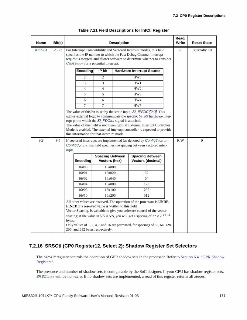
7.2 CP0 Register Descriptions
MIPS32® 1074K™ CPU Family Software User’s Manual, Revision 01.03 171
7.2.16 SRSCtl (CP0 Register12, Select 2): Shadow Register Set Selectors
The SRSCtl register controls the operation of GPR shadow sets in the processor. Refer to Section 6.4 “GPR ShadowRegisters”.
The presence and number of shadow sets is configurable by the SoC designer. If your CPU has shadow register sets,SRSCtlHSS will be non-zero. If no shadow sets are implemented, a read of this register returns all zeroes.
IPFDCI 25:23 For Interrupt Compatibility and Vectored Interrupt modes, this fieldspecifies the IP number to which the Fast Debug Channel Interruptrequest is merged, and allows software to determine whether to considerCauseFDCI for a potential interrupt.
The value of this bit is set by the static input, SI_IPFDCI[2:0]. Thisallows external logic to communicate the specific SI_Int hardware inter-rupt pin to which the SI_FDCInt signal is attached.The value of this field is not meaningful if External Interrupt ControllerMode is enabled. The external interrupt controller is expected to providethis information for that interrupt mode.
R Externally Set
VS 9:5 If vectored interrupts are implemented (as denoted by Config3VInt orConfig3VEIC), this field specifies the spacing between vectored inter-rupts.
All other values are reserved. The operation of the processor is UNDE-FINED if a reserved value is written to this field.Vector Spacing. Is writable to give you software control of the vector
spacing; if the value in VS is VS, you will get a spacing of 32 × 2(VS-1)
bytes.Only values of 1, 2, 4, 8 and 16 are permitted, for spacings of 32, 64, 128,256, and 512 bytes respectively.
R/W 0
Table 7.21 Field Descriptions for IntCtl Register
Name Bit(s) DescriptionRead/Write Reset State
Encoding IP bit Hardware Interrupt Source
2 2 HW0
3 3 HW1
4 4 HW2
5 5 HW3
6 6 HW4
7 7 HW5
EncodingSpacing Between
Vectors (hex)Spacing BetweenVectors (decimal)
16#00 16#000 0
16#01 16#020 32
16#02 16#040 64
16#04 16#080 128
16#08 16#100 256
16#10 16#200 512

CP0 Registers of the 1074K™ CPU
172 MIPS32® 1074K™ CPU Family Software User’s Manual, Revision 01.03
Figure 7.17 SRSCtl Register Format31 30 29 26 25 22 21 18 17 16 15 12 11 10 9 6 5 4 3 0
0 HSS 0 EICSS 0 ESS 0 PSS 0 CSS
Table 7.22 Field Descriptions for SRSCtl Register
Name Bit(s) DescriptionRead/Write Reset State
HSS 29:26 Highest Shadow Set. This field contains the highest shadow set numberthat is implemented by this processor (i.e., the number of available regis-ter sets minus 1). A value of zero in this field indicates that only the regu-lar GPRs are implemented.Possible values of this field for the 1074K processor are:The value in this field also represents the highest value that can be writtento the ESS, EICSS, PSS, and CSS fields of this register, or to any ofthe fields of the SRSMap register. The operation of the processor isUNDEFINED if a value larger than the one in this field is written to anyof those other fields
R Preset
EICSS 21:18 External Interrupt Controller Shadow Set. If Config3VEIC is 1 (EIC inter-rupt mode is enabled), this field is loaded from the external interrupt con-troller for each interrupt request and is used in place of the SRSMapregister to select the current shadow set for the interrupt. See Section6.3.1.3 “External Interrupt Controller Mode” for a discussion of EICinterrupt mode. If Config3VEIC is 0, this field returns zero on reads.
R Undefined
ESS 15:12 Exception Shadow Set. This field specifies the shadow set to use on entryto Kernel Mode caused by any exception other than a vectored interrupt.The operation of the processor is UNDEFINED if software writes avalue in this field that is greater than the value in the HSS field.
R/W 0
PSS 9:6 Previous Shadow Set. If GPR shadow registers are implemented, with theexclusions noted in the next paragraph, this field is copied from the CSSfield when an exception or interrupt occurs. An eret instruction copiesthis value back into the CSS field if StatusBEV = 0.This field is not updated on any exception which sets StatusERL to 1(i.e., Reset, Soft Reset, NMI, cache error), an entry into EJTAG Debugmode, or any exception or interrupt that occurs with StatusEXL = 1 orStatusBEV = 1, or StatusERL = 1.The operation of the processor is UNDEFINED if software writes avalue into this field that is greater than the value in the HSS field.
R/W 0

7.2 CP0 Register Descriptions
MIPS32® 1074K™ CPU Family Software User’s Manual, Revision 01.03 173
7.2.17 SRSMap (CP0 Register 12, Select 3): Shadow Set Choice for Each InterruptLevel in VI Mode
The SRSMap register specifies the mapping of a vector number to a shadow register set number for use when servic-ing an interrupt in Vectored Interrupt (VI) mode (Config3VInt = 1, Config3VEIC = 0, and CauseIV = 1). The values inthis register are not used for non-interrupt exceptions or non-vectored interrupts (CauseIV = 0 or IntCtlVS = 0); in thesecases, the shadow set number is the value in SRSCtlESS.
If SRSCtlHSS is zero (indicating that no shadow sets are implemented), the result of a software read or write of thisregister is UNPREDICTABLE.
The operation of the processor is UNDEFINED if a value is written to any field in this register that is greater than thevalue of SRSCtlHSS.
The same shadow set number can be used for multiple interrupt vectors, creating a many-to-one mapping from a vec-tor to a single shadow register set number. In Interrupt Compatibility mode, one shadow set can be used for all excep-tion handlers, including interrupt handlers, by setting SRSCtlESS to a non-zero value.
CSS 3:0 Current Shadow Set. If GPR shadow registers are implemented, this fieldis the number of the current GPR set. With the exclusions noted in thenext paragraph, this field is updated with a new value on any interrupt orexception, and restored from the PSS field on an eret. Table 7.23describes the various sources from which the CSS field is updated on anexception or interrupt.This field is not updated on any exception which sets StatusERL to 1(i.e., Reset, Soft Reset, NMI, cache error), an entry into EJTAG Debugmode, or any exception or interrupt that occurs with StatusEXL = 1, orStatusBEV = 1. Neither is it updated on an eret with StatusERL = 1 orStatusBEV = 1. This field is not updated on an exception that occurswhile StatusERL = 1.The value of CSS can be changed directly by software only by writingthe PSS field and executing an eret instruction.
R 0
Table 7.23 Sources for SRSCtlCSS on an Exception or Interrupt
Exception Type Condition SRSCtlCSS Source Comment
Exception All SRSCtlESS
Non-Vectored Interrupt CauseIV = 0 SRSCtlESS Treat as exception
Vectored Interrupt CauseIV = 1 andConfig3VEIC = 0 and
Config3VInt = 1
SRSMapVECTNUM Source is internal map register.(for VECTNUM see Table 6.4).
Vectored EIC Interrupt CauseIV = 1 andConfig3VEIC = 1
SRSCtlEICSS Source is external interruptcontroller.
Table 7.22 Field Descriptions for SRSCtl Register (Continued)
Name Bit(s) DescriptionRead/Write Reset State

CP0 Registers of the 1074K™ CPU
174 MIPS32® 1074K™ CPU Family Software User’s Manual, Revision 01.03
In EIC interrupt mode, this register has no effect, and the shadow set number to be used is determined by an input busfrom the external interrupt controller.
Figure 7.18 SRSMap Register Format
7.2.18 Cause (CP0 Register 13, Select 0): Cause of Last General Exception
The Cause register describes the cause of the most recent exception and controls software interrupt requests and thevector through which interrupts are dispatched. With the exception of the IP1..0, DC, IV, and WP fields, all fields inthe Cause register are read-only. IP7..2 are interpreted as the Requested Interrupt Priority Level (RIPL) in ExternalInterrupt Controller (EIC) interrupt mode.
Figure 7.19 Cause Register Format
31 28 27 24 23 20 19 16 15 12 11 8 7 4 3 0
SSV7 SSV6 SSV5 SSV4 SSV3 SSV2 SSV1 SSV0
Table 7.24 Field Descriptions for SRSMap Register
Name Bit(s) DescriptionRead/Write Reset State
SSV7 31:28 Shadow register set number for Vector Number 7 R/W 0
SSV6 27:24 Shadow register set number for Vector Number 6 R/W 0
SSV5 23:20 Shadow register set number for Vector Number 5 R/W 0
SSV4 19:16 Shadow register set number for Vector Number 4 R/W 0
SSV3 15:12 Shadow register set number for Vector Number 3 R/W 0
SSV2 11:8 Shadow register set number for Vector Number 2 R/W 0
SSV1 7:4 Shadow register set number for Vector Number 1 R/W 0
SSV0 3:0 Shadow register set number for Vector Number 0 R/W 0
31 30 29 28 27 26 25 24 23 22 21 20 16 15 10 9 8 7 6 2 1 0
BD TI CE DC PCI 0 IV WP FDCI 0 IP7-2 IP1-0 0 ExcCode 0

7.2 CP0 Register Descriptions
MIPS32® 1074K™ CPU Family Software User’s Manual, Revision 01.03 175
Table 7.25 Field Descriptions for Cause Register
Name Bit(s) DescriptionRead/Write Reset State
BD 31 Indicates whether the last exception taken occurred in a branch delayslot:
The processor updates BD only if the EXL bit in the Status register waszero when the exception occurred.
If the exception occurred in a branch delay slot, EPC is set to restart exe-cution at the branch, which is usually the correct thing to do. You need toconsult CauseBD only when you need to look at the instruction whichcaused the exception (perhaps to emulate it).
R Undefined
TI 30 Timer Interrupt. Denotes whether a timer interrupt is pending (analogousto the IP bits for other interrupt types):
The state of this bit is available on the external CPU interface as theSI_TimerInt signal.
See also the descriptions of the Count and Compare registers.
R Undefined
CE 29:28 Coprocessor unit number referenced when a Coprocessor Unusableexception is taken. This field is loaded by hardware on every exception,but is UNPREDICTABLE for all exceptions except Coprocessor Unus-able.
R Undefined
DC 27 Disable Count register. In some power-sensitive applications, the Countregister is not used but may still be the source of some noticeable powerdissipation. This bit allows the Count register to be stopped in such situ-ations, for example, during low-power operation following a waitinstruction.
R/W 0
Encoding Meaning
0 Not in delay slot
1 In delay slot
Encoding Meaning
0 No timer interrupt is pending
1 Timer interrupt is pending
Encoding Meaning
0 Enable counting of Count register
1 Disable counting of Count register
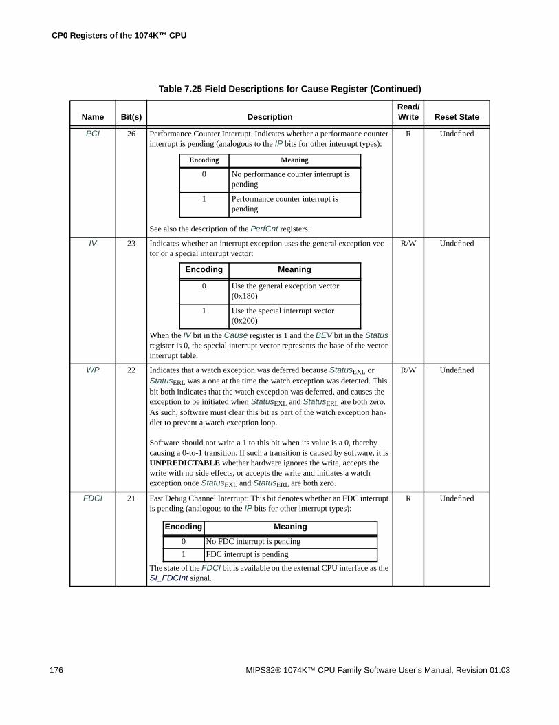
CP0 Registers of the 1074K™ CPU
176 MIPS32® 1074K™ CPU Family Software User’s Manual, Revision 01.03
PCI 26 Performance Counter Interrupt. Indicates whether a performance counterinterrupt is pending (analogous to the IP bits for other interrupt types):
See also the description of the PerfCnt registers.
R Undefined
IV 23 Indicates whether an interrupt exception uses the general exception vec-tor or a special interrupt vector:
When the IV bit in the Cause register is 1 and the BEV bit in the Statusregister is 0, the special interrupt vector represents the base of the vectorinterrupt table.
R/W Undefined
WP 22 Indicates that a watch exception was deferred because StatusEXL orStatusERL was a one at the time the watch exception was detected. Thisbit both indicates that the watch exception was deferred, and causes theexception to be initiated when StatusEXL and StatusERL are both zero.As such, software must clear this bit as part of the watch exception han-dler to prevent a watch exception loop.
Software should not write a 1 to this bit when its value is a 0, therebycausing a 0-to-1 transition. If such a transition is caused by software, it isUNPREDICTABLE whether hardware ignores the write, accepts thewrite with no side effects, or accepts the write and initiates a watchexception once StatusEXL and StatusERL are both zero.
R/W Undefined
FDCI 21 Fast Debug Channel Interrupt: This bit denotes whether an FDC interruptis pending (analogous to the IP bits for other interrupt types):
The state of the FDCI bit is available on the external CPU interface as theSI_FDCInt signal.
R Undefined
Table 7.25 Field Descriptions for Cause Register (Continued)
Name Bit(s) DescriptionRead/Write Reset State
Encoding Meaning
0 No performance counter interrupt ispending
1 Performance counter interrupt ispending
Encoding Meaning
0 Use the general exception vector(0x180)
1 Use the special interrupt vector(0x200)
Encoding Meaning
0 No FDC interrupt is pending
1 FDC interrupt is pending

7.2 CP0 Register Descriptions
MIPS32® 1074K™ CPU Family Software User’s Manual, Revision 01.03 177
IP7-2 15:10 Indicates an interrupt is pending:
If EIC interrupt mode is not enabled (Config3VEIC = 0), timer interruptsare combined in a system-dependent way with any hardware interrupt. IfEIC interrupt mode is enabled (Config3VEIC = 1), these bits take on adifferent meaning and are interpreted as the RIPL field, described below.See Section 6.3 “Interrupts” for a general description of interrupt pro-cessing.
R Undefined
IP1-0 9:8 Controls the request for software interrupts:
These bits are exported to an external interrupt controller for prioritiza-tion in EIC interrupt mode with other interrupt sources. The state of thesebits is available on the external CPU interface as the SI_SWInt[1:0] bus.
R/W Undefined
ExcCode 6:2 Encodes the cause of the last exception as described in Table 7.26. R Undefined
Table 7.26 Exception Code values in ExcCode Field of Cause Register
Value Code What just happened?
0 Int Interrupt
1 Mod Store, but page marked as read-only in the TLB
2 TLBL Load or fetch, but page marked as invalid in the TLB
3 TLBS Store, but page marked as invalid in the TLB
4 AdEL Address error on load/fetch or store respectively. Address is either wrongly aligned, or a privi-lege violation.5 AdES
6 IBE Bus error signaled on instruction fetch
7 DBE Bus error signaled on load/store (imprecise)
8 Sys System call, i.e. syscall instruction executed.
9 Bp Breakpoint, i.e. break instruction executed.
10 RI Instruction code not recognized (or not legal)
11 CpU Instruction code was for a co-processor which is not enabled in StatusCU3-0.
Table 7.25 Field Descriptions for Cause Register (Continued)
Name Bit(s) DescriptionRead/Write Reset State
Bit Name Meaning
15 IP7 Hardware interrupt 5
14 IP6 Hardware interrupt 4
13 IP5 Hardware interrupt 3
12 IP4 Hardware interrupt 2
11 IP3 Hardware interrupt 1
10 IP2 Hardware interrupt 0
Bit Name Meaning
9 IP1 Request software interrupt 1
8 IP0 Request software interrupt 0

CP0 Registers of the 1074K™ CPU
178 MIPS32® 1074K™ CPU Family Software User’s Manual, Revision 01.03
7.2.19 EPC (CP0 Register 14, Select 0): Restart Address from Exception
Following an exception other than a debug or error or debug exception, the Exception Program Counter (EPC) con-tains the address at which processing resumes after the exception has been serviced. (The corresponding debug anderror exception use DEPC and ErrorEPC respectively.)
Unless the EXL bit in the Status register is set (indicating, among other things, that interrupts are disabled), the pro-cessor writes the EPC register when an exception occurs.
• For synchronous (precise) exceptions, EPC contains either:
• the virtual address of the instruction that was the direct cause of the exception, or
• the virtual address of the immediately preceding branch or jump instruction, when the exception causinginstruction is in a branch delay slot, and the Branch Delay bit in the Cause register is set.
• For asynchronous (imprecise) exceptions, EPC contains the address of the instruction at which to resume execu-tion.
The processor reads the EPC register as the result of execution of the eret instruction.
12 Ov Overflow from a trapping variant of integer arithmetic instructions.
13 Tr Condition met on one of the conditional trap instructions teq etc.
14 - Reserved
15 FPE Floating point unit exception — more details in the FPU control/status registers.
16-17 - Available for implementation-dependent use.
19-22 - Reserved
23 WATCH Instruction or data reference matched a watchpoint.
24 MCheck "Machine check"
25 Thread Thread-related exception, only for CPUs supporting the MIPS MT ASE. In that case the causeis further detailed in VPEControlEXCPT.
26 DSP Tried to run an instruction from the MIPS DSP ASE, but it’s either not enabled or not avail-able. In particular, StatusMX is zero).
27-29 - Reserved
30 CacheErr Parity/ECC error somewhere in the CPU, on either instruction fetch, load or cache refill. Infact you never see this value in CauseExcCode; but some of the codes in this table includingthis one can be visible in the "debug mode" of the EJTAG debug unit — see and in particularthe notes on the Debug register.
31 - Reserved
Table 7.26 Exception Code values in ExcCode Field of Cause Register
Value Code What just happened?

7.2 CP0 Register Descriptions
MIPS32® 1074K™ CPU Family Software User’s Manual, Revision 01.03 179
Figure 7.20 EPC Register Format
7.2.20 PRId (CP0 Register 15, Select 0): Processor Identification and Revision
The Processor Identification (PRId) register is a 32 bit read-only register that contains information identifying themanufacturer, manufacturer options, processor identification, and revision level of the processor.
Figure 7.21 PRId Register Format
31 0
EPC
Table 7.27 EPC Register Field Description
Fields
DescriptionRead /Write Reset StateName Bit(s)
EPC 31:0 Exception Program Counter. R/W Undefined
31 24 23 16 15 8 7 0
CoOpt CoID Imp Rev
Table 7.28 Field Descriptions for PRId Register
Name Bit(s) DescriptionRead/Write Reset State
CoOpt 31:24 Company Option. Whatever is specified by the SoC builder who synthe-sizes the CPU— refer to your SoC manual. It should be a numberbetween 0 and 127— higher values are reserved by MIPS Technologies.
R Preset
CoID 23:16 Company ID. Identifies the company that designed or manufactured theprocessor. In the 1074K, this field contains a value of 1 to indicate MIPSTechnologies, Inc.
R 1
Imp 15:8 Processor ID. Identifies the type of processor. This field allows softwareto distinguish between the various types of processors from MIPS Tech-nologies. The value of this field is 0x9a for the 1074K CPU.
R 0x9a
Rev 7:0 The revision number of the CPU design. R Preset
Bit(s) Name Meaning
7:5 MajorRevision
This number is increased on majorrevisions of the CPU
4:2 MinorRevision
This number is increased on eachincremental revision of the processorand reset on each new major revision
1:0 PatchLevel
If a patch is made to modify an olderrevision of the processor, this field willbe incremented

CP0 Registers of the 1074K™ CPU
180 MIPS32® 1074K™ CPU Family Software User’s Manual, Revision 01.03
7.2.21 EBase (CP0 Register 15, Select 1): Exception entry point base address andCPU/VPE ID
The EBase register is a read/write register containing the base address of the exception vectors used when StatusBEVequals 0, and a read-only CPU number value that may be used by software to distinguish different processors in amulti-processor system.
The EBase register provides the ability for software to identify the specific processor within a multi-processor sys-tem, and allows the exception vectors for each processor to be different, especially in systems composed of heteroge-neous processors. Bits 31:12 of the EBase register are concatenated with zeros to form the base of the exceptionvectors when StatusBEV is 0. The exception vector base address comes from the fixed defaults (see Section6.5 “Exception Vector Locations”) when StatusBEV is 1, or for any EJTAG Debug exception. The reset state of bits31:12 of the EBase register initialize the exception base register to 16#8000.0000, providing backward compati-bility with Release 1 implementations.
Bits 31:30 of the EBase Register are fixed with the value 2#10 to force the exception base address to be in the kseg0or kseg1 unmapped virtual address segments. Bit 29 of exception base address will be forced to 1 on Cache Errorexceptions so the exception handler will be executed from the uncached kseg1 segment.
If the value of the exception base register is to be changed, this must be done with StatusBEV equal 1. The operationof the processor is UNDEFINED if the Exception Base field is written with a different value when StatusBEV is 0.
Combining bits 31:12 with the Exception Base field allows the base address of the exception vectors to be placed atany 4KBbyte page boundary.
Figure 7.22 EBase Register Format31 30 29 12 11 10 9 0
1 0 VA 0 CPUNum
Table 7.29 Field Descriptions for EBase Register
Name Bit(s) DescriptionRead/Write Reset State
VA 29:12 The base address for the exception vectors, adjustable to a resolution of4Kbytes. See the exception entry points table for how that moves all theexception entry points.The top two bits of this register must be 10 to make sure the exceptionvector ends up in kseg0, conventionally used for OS code.By setting EBase in any CPU to a unique value, that CPU can have itsown unique exception handlers.Write this field only when StatusBEV is set so that any exception will behandled through the ROM entry points (otherwise you would be chang-ing the exception address under your own feet, and the results of that areundefined).
R/W 0x0000.0
CPUNum 9:0 This field contains an identifier that will be unique among the CPUs in amulti-processor system. The value in this field is set by theSI_CPUNum[9:0] static input pins to the CPU.
R Externally Set

7.2 CP0 Register Descriptions
MIPS32® 1074K™ CPU Family Software User’s Manual, Revision 01.03 181
7.2.22 CDMMBase Register (CP0 Register 15, Select 2)
The 36-bit physical base address for the Common Device Memory Map facility is defined by this register. This regis-ter only exists if Config3CDMM is set to one.
Figure 7.23 shows the format of the CDMMBase register, and Table 7.30 describes the register fields.
Figure 7.23 CDMMBase Register
31 28 27 11 10 9 8 0
0 CDMM_UPPER_ADDR EN CI CDMMSize
Table 7.30 CDMMBase Register Field Descriptions
Fields
DescriptionRead /Write
ResetStateName Bits
CDMM_UPPER_ADDR
27:11 Bits 31:15 of the base physical address of the commondevice memory-mapped registers.
R/W Undefined
EN 10 Enables the CDMM region.If this bit is cleared, memory requests to this addressregion go to regular system memory. If this bit is set,memory requests to this region go to the CDMM logic
R/W 0
CI 9 If set to 1, this indicates that the first 64-byte Device Reg-ister Block of the CDMM is reserved for additional regis-ters which manage CDMM region behavior and are not IOdevice registers.This feature is not implemented and this field will read as0.
R 0
CDMMSize 8:0 This field represents the number of 64-byte Device Regis-ter Blocks instantiated in the CPU.
R 2
Encoding Meaning
0 CDMM region is disabled.
1 CDMM region is enabled.
Encoding Meaning
0 1 DRB
1 2 DRBs
2 3 DRBs
... ...
511 512 DRBs

CP0 Registers of the 1074K™ CPU
182 MIPS32® 1074K™ CPU Family Software User’s Manual, Revision 01.03
7.2.23 CMGCR Base Register (CP0 Register 15, Select 3)
This register defines the 36-bit physical base address for the memory-mapped Coherency Manager Global Configura-tion Register space. This register only exists if Config3CMGCR is set to one.
Figure 7.24 shows the format of the CMGCRBase register, and Table 7.31 describes the register fields.
Figure 7.24 CMGCRBase Register
7.2.24 Config (CP0 Register 16, Select 0): Legacy Configuration Register
The main role of the (several) configuration registers is to be a read-only repository of information about the CPU’sresources, encoded so as to be useful to operating system initialization code.
But this original Config register acquired some writable fields. Typically, these select the sort of options you’d writeonce in initialization software and then never touch again.
Figure 7.25 Config Register Format
31 11 10 0
CMGCR_BASE_ADDR 0
Table 7.31 CMGCRBase Register Field Descriptions
Fields
DescriptionRead /Write
ResetStateName Bits
CMGCR_BASE_ADDR
31:11 Bits 35:15 of the base physical address of the memory-mapped Coherency Manager Global Configuration regis-ters.The number of implemented physical address bits isimplementation-specific. For the unimplemented addressbits, writes are ignored, reads return zero.The reset value is set when the core is configured using theConfiguration GUI.
R Preset
0 10:0 Must be written as zero; returns zero on read R 0
31 30 28 27 25 24 23 22 21 20 19 18 17 16 15 14 13 12 10 9 7 6 4 3 2 0
M K23 KU ISP DSP UDI SB 0 WC MM 0 BM BE AT AR MT 0 VI K0
Table 7.32 Field Descriptions for Config Register
Name Bit(s) DescriptionRead/Write Reset State
M 31 Reads 1 if Config1 is available. R 1

7.2 CP0 Register Descriptions
MIPS32® 1074K™ CPU Family Software User’s Manual, Revision 01.03 183
K23 30:28 If your CPU uses fixed mapping instead of having a TLB, you set thecacheability attributes of chunks of the memory map by writing thesefields. They’re encoded like EntryLo0-1C.If you have a TLB, these fields are unused (but please write only zero tothem).ConfigK23 is for program addresses 0xC000.0000-0xFFFF.FFFF(the "kseg2" and "kseg3" areas), while ConfigKU is for programaddresses 0x0000.0000-0x7FFF.FFFF (the "kuseg" area)From reset, both are "uncached" (code 2).
FMT:R/W
TLB: R
FMT:2TLB:0
KU 27:25 FMT:R/W
TLB: R
FMT:2TLB:0
ISP 24 Reads 1 if I-side scratchpad (ISPRAM) is fitted. R Preset
DSP 23 Reads 1 if D-side scratchpad (SPRAM) is fitted.(Don’t confuse this with the MIPS DSP ASE, whose presence is indi-cated by Config3DSPP.)
R Preset
UDI 22 Reads 1 if your CPU implements user-defined "CorExtend" instructions. R Preset
SB 21 Read-only "SimpleBE" bus mode indicator, which reflects the CPU inputsignal SI_SimpleBE.If set, means that this CPU will only do simple partial-word transfers onits OCP interface; that is, the only partial-word transfers will be byte,aligned half-word, and aligned word.If zero, it may generate partial-word transfers with an arbitrary set ofbytes enabled (which some memory controllers may not like).
R Externally Set
WC 19 Write Control. Enable write control of cache size andspecial function bits in the Config1 register.0: Write control disabled1: Write control enabled
R/W 0
MM 18 Writable: set 1 if you want writes resulting from separate store instruc-tions in write-through mode merged into a single (possibly burst) transac-tion at the interface. Write-through caching is not supported on 1074KCPU, so this bit is not relevant. This doesn’t affect cache writebacks(which are always whole blocks together) or uncached writes (which arenever merged).
R/W 1
BM 16 Read-only. Reads 0 when bus uses sequential burst order and reads 1when it uses sub-block burst order; set by the CPU input signalSI_SBlock signal to match your system controller. The 1074K CPUonly support Sequential burst order.
R 0
BE 15 Reads 1 for big-endian, 0 for little-endian, as selected by the CPU inputSI_Endian.
R Externally Set
AT 14:13 Reads 0 for MIPS32. R 0
AR 12:10 Reads 2 to reflect Release 2 of the MIPS32 architecture. Zero is for theoriginal release.
R 1
Table 7.32 Field Descriptions for Config Register (Continued)
Name Bit(s) DescriptionRead/Write Reset State
0 MIPS32
1 MIPS64 instruction set but MIPS32 address map
2 MIPS64 instruction set with full address map

CP0 Registers of the 1074K™ CPU
184 MIPS32® 1074K™ CPU Family Software User’s Manual, Revision 01.03
7.2.25 Config1-2 (CP0 Register 16, Select 1-2): MIPS32/64 Configuration Registers
These two registers tell you the size of the TLB, and the size and organization of L1, L2, and L3 caches (a zero "linesize" is used to indicate a cache which isn’t there).
Config2 also has fields which tell you about the presence of some extensions to the base MIPS32 architecture that areimplemented on this CPU.
7.2.25.1 Config1
This register displays the size and configuration of the TLB and primary caches, and the availability of some optionalCPU features.
Figure 7.26 Config1 Register Format
MT 9:7 MMU type:
All MIPS Technologies cores are type 1 or 3, as selected by your SoCbuilder.
R Preset
VI 3 Reads 0 to indicate L1 I-cache is physically tagged. It would read 1 if theL1 I-cache were virtual (both indexed and tagged using virtual address).
R 0
K0 2:0 Kseg0 coherency attribute of the page. See Table 7.8 for the field encod-ing.
R/W 2
31 30 25 24 22 21 19 18 16 15 13 12 10 9 7 6 5 4 3 2 1 0
M MMUSize IS IL IA DS DL DA C2 MD PC WR CA EP FP
Table 7.33 Field Descriptions for Config1 Register
Name Bit(s) Description Read/ Write Reset State
M 31 Continuation bit, set to 1 to indicate that Config2 is implemented. R 1
MMUSize 30:25 The size of the TLB array (the array has MMUSize +1 entries). R Preset
Table 7.32 Field Descriptions for Config Register (Continued)
Name Bit(s) DescriptionRead/Write Reset State
0 None
1 MIPS32/64 compliant TLB
2 "BAT" type
3 MIPS-standard fixed mapping

7.2 CP0 Register Descriptions
MIPS32® 1074K™ CPU Family Software User’s Manual, Revision 01.03 185
7.2.25.2 Config2
Figure 7.27 Config2 Register Format
IS 24:22 Fields for the L1 I-cache. All caches have the same triplet of fields, whichreport:
So if (IS, IL, IA) is (2,4,3), you have 256 sets/way, 32 bytes per line, and 4-way set associativity, which is a 32Kbyte cache.1074K family cores always have 32-byte cache lines. The L1 caches are 4-wayset associative and are 16KB, 32KB, or 64KB. L1 I-cache of 0KB is supported.
RR/W when
config.WC isset
Preset
IL 21:19 RR/W when
config.WC isset
4
IA 18:16 R 3
DS 15:13 For L1 D-cache: same encoding as Config1IS,IL,IA.The cache line size is fixed at 32 bytesand L1-D-cache of 16KB, 32Kb, and64KB are supported.
RR/W when
config.WC isset
Preset
DL 12:10 RR/W when
config.WC isset
Preset
DA 9:7 R 3
C2 6 the absence of a coprocessor 2 (that would be a customer-designed coproces-sor).
R 0
MD 5 0 to indicate that the MDMX ASE is not implemented in the floating point unitof the 1074K CPU
R 0
PC 4 There is at least one performance counter implemented, see PerfCnt0-3. R 1
WR 3 Reads 1 because the 1074K CPU always has watchpoint registers, seeWatchLo0-3/WatchHi0-3.
R 1
CA 2 Reads 1 because the MIPS16e compressed-code instruction set is available (asit is on most MIPS Technologies cores).
R 1
EP 1 Reads 1 because an EJTAG debug unit is always provided on MIPS Technolo-gies cores.
R 1
FP 0 A floating point unit is attached. R Preset
31 30 28 27 24 23 20 19 16 15 13 12 11 8 7 4 3 0
M TU TS TL TA SU L2B SS SL SA
Table 7.33 Field Descriptions for Config1 Register
Name Bit(s) Description Read/ Write Reset State
S Number of sets per way. Calculate as: 64 x 2S
L Line size. Zero means no cache at all, otherwise calculate as:
2 × 2L
A Associativity/number of ways. Calculate as A + 1

CP0 Registers of the 1074K™ CPU
186 MIPS32® 1074K™ CPU Family Software User’s Manual, Revision 01.03
7.2.26 Config3 (CP0 Register 16, Select 3): Configuration register showing ASEs
Config3 provides information about the presence of optional extensions to the base MIPS32 architecture in addition tothose specified in Config2.
Figure 7.28 Config3 Register Format
Table 7.34 Field Descriptions for Config2 Register
Name Bit(s) Description Read/ Write Reset State
M 31 Continuation bit, 1 if Config3 is implemented. R 1
TU 30:28 Reserved for extra control/status bits for an L3 cache, if fitted. R 0
TS 27:24 If Config2TL is non-zero, your CPU has an L3 (tertiary) cache. Its size andshape are encoded as Config1IS,IL,IA described above. However, no 1074Kfamily CPU is equipped for an L3 cache.
R 0
TL 23:20 R 0
TA 19:16 R 0
SU 15:13 Reserved for more secondary cache control/status bits, when required. Notused on the 1074K family cores.
R 0
L2B 12 L2_Bypass/L2_Bypassed. In systems which include an L2 cache, writing a1 to this bit, will set the L2_Bypass output from the CPU. Setting theL2_Bypass output, directs the L2 cache to go into bypass mode, L2responds by assertion its L2_Bypassed output pin. The value ofL2_Bypassed is returned when L2B is read. When this bit is set through awrite operation, a subsequent read of this bit will not indicate a 1, until theL2 has asserted the signal L2_Bypassed indicating that it has beenbypassed.
R/W 0
SS 11:8 If Config2SL is non-zero, your CPU has an external L2 (secondary) cache.Its size and shape are encoded as in Config1IS,IL,IA above.
RR/W when
config.WC isset
Preset
SL 7:4 RR/W when
config.WC isset
Preset
SA 3:0 RR/W when
config.WC isset
Preset
31 30 29 28 14 13 12 11 10 9 8 7 6 5 4 3 2 1 0
M 0 CMGCR 0 ULRI 0 DSP2P DSPP CTXTC 0 VEIC VInt SP CDMM MT SM TL

7.2 CP0 Register Descriptions
MIPS32® 1074K™ CPU Family Software User’s Manual, Revision 01.03 187
7.2.27 Config6 (CP0 Register 16, Select 6)
Config3 provides information about the presence of optional extensions to the base MIPS32 architecture in addition tothose specified in Config2 and Config3.
Figure 7.29 Config6 Register Format
Table 7.35 Field Descriptions for Config3 Register
Name Bit(s) DescriptionRead/Write Reset State
M 31 Continuation bit, zero because there is no Config4. R 0
CMGCR 29 Reads 1 to indicate that a Global Control Register in the Coherence Man-ager is implemented.
R 1
ULRI 13 Reads 1 to indicate that the UserLocal Register is implemented R 1
DSP2P 11 Reads 1 to indicate that Revision 2 of the MIPS DSP ASE is implemented R 1
DSPP 10 Reads 1 to indicate that the MIPS DSP ASE extension is implemented. R 1
CTXTC 9 Reads 1 to indicate the ContextConfig register is implemented. The widthof the BadVPN2 field in the Context register depends on the contents ofthis register.
R 1
VEIC 6 Read-only bit from the CPU input signal SI_EICPresent, which should beset in the SoC to alert software to the availability of an EIC-compatibleinterrupt controller.
R Externally Set
VInt 5 Reads 1 to indicate the CPU can handle vectored interrupts. R 1
SP 4 Reads 0 to indicate the CPU does not support small (1Kbyte) pages. R 0
CDMM 3 Reads 1 to indicate the Common Device Memory Map is implemented. R 1
MT 2 Reads 0 to indicate the CPU does not include the MIPS MT (multithread-ing) ASE.
R 0
SM 1 Reads 0 to indicate the CPU does not include the instructions of the Smart-MIPS ASE.
R 0
TL 0 Reads1 to indicate instruction trace is supported. R 0
31 15 14 13 12 10 9 8 7 2 1 0
0 SPCD SYND IFUPerfCtl NMRUP NMRUD 0 JRCP JRCD

CP0 Registers of the 1074K™ CPU
188 MIPS32® 1074K™ CPU Family Software User’s Manual, Revision 01.03
Table 7.36 Field Descriptions for Config6 Register
Name Bit(s) DescriptionRead/Write Reset State
SPCD 14 Sleep state Performance Counter Disable. When this bit is set, the perfor-mance counter CPU clocks are prevented from shutting down.The primary use of this bit is to keep performance counters alive when theCPU is in sleep mode.
R/W 0
SYND 13 Synonym tag update Disable. This bit controls the tag update behavior forloads with a Virtual Address miss but a Physical Address hit during a D-cache look-up.
R/W 0
Encoding Meaning
0 Performance counter operation is enabledin Sleep state.
1 Performance counter operation is disabledin Sleep state.
Encoding Meaning
0 Synonym load misses will opportunisti-cally update the tag so that subsequentloads will hit (virtual address hit) at lookup.
1 Synonym load misses at lookup will notupdate the tag with new information.

7.2 CP0 Register Descriptions
MIPS32® 1074K™ CPU Family Software User’s Manual, Revision 01.03 189
IFUPerfCtl 12:10 IFU Performance Control. This field encodes IFU events that provide debugand performance information for the IFU pipeline.
Lost IDU bandwidth occurs when the IDU is accepting instructions, butinstructions are not being provided by the IFU. The count of these eventscan be seen via Performance Counters 0 or 3, and the event number 11. Inorder to view the IFU Perf Ctl events, the Performance Counter Controlneeds to be programmed accordingly Table 7.50, "Performance CounterEvents and Codes" for general information on event number 11.
R/W 0
NMRUP 9 NMRU Present. Rather than a fully random replacement on TLBWR, atable of the most recently used JTLB entries is maintained, whose entriesare not replaced whenever possible.
R 1
NMRUD 8 NMRU Disable. Disable bit for NMRU JTLB replacement scheme. R/W 0
Table 7.36 Field Descriptions for Config6 Register (Continued)
Name Bit(s) DescriptionRead/Write Reset State
Encoding Meaning
000 IDU is accepting instructions, but IFU is notproviding any.
001 A control transfer instruction such as abranch or jump causes lost IDU bandwidth.
010 A stalled instruction such as an unpredictedjump must wait for an address and thuscauses lost IDU bandwidth.
011 Cache prediction was correct.
100 Cache prediction was incorrect.
101 Cache did not predict due to invalid JRcache entry, or the instruction tag miscom-pared with tag in JR cache.
110 Unimplemented.
111 Condition branch was taken.
Encoding Meaning
0 Most Recently Used JTLB replacementscheme not present.
1 Most Recently Used JTLB replacementscheme present.
Encoding Meaning
0 TLBWR instruction uses NMRU scheme.
1 TLBWR instruction uses random replace-ment.

CP0 Registers of the 1074K™ CPU
190 MIPS32® 1074K™ CPU Family Software User’s Manual, Revision 01.03
7.2.28 Config7 (CP0 Register 16, Select 7): CPU-specific Configuration
This register controls machine-specific features of the 1074K CPU. A few of them are for hardware interface adapta-tion, but most are for chip or system test only. They default into a "safe" value, and most software—even bootstrapsoftware—can and should ignore these registers.
Figure 7.30 Config7 Register Format
JRCP 1 JR Cache Present. JR cache learns the target address of "Jump Register"type instructions and subsequently predicts that target address.
R 1
JRCD 0 JR Cache Prediction Disable. Disables JR target address prediction.. R/W 0
31 30 29 28 27 26 25 24 23 22 21 20 19 18 17 16 15 13 12 11 10 9 8 7 6 5 4 3 2 1 0
WII FPFS IHB FPR1 SEHB CP2IO IAGN IALU DGHR SG SUI 0 HCI FPR0 AR 0 PREF IAR IVA ES 0 CP1IO 0 ULB BP RPS BHT SL
Table 7.37 Field Descriptions for Config7 Register
Name Bit(s) DescriptionRead/Write Reset State
WII 31 Wait IE Ignore. When this bit is set, an interrupt will unblock a waitinstruction, even if StatusIE is preventing the interrupt from being taken.If WII reads 0, the 1074K CPU remains in the wait condition forever ifentered with interrupts disabled. If set to 1, it allows OS code to avoidtricky race conditions.
R 1
FPFS 30 Fast Prepare for Store. When this bit is set, pref 31 will behave asspecified, i.e., the prefetch instruction will only validate the data tag butnot write 0’s into the data cache.By default, this bit will be 0 and pref 31 will behave like pref 30.This means that pref 31 will validate the data tag and write 0’s intothe data cache array for the specified line,
R/W 0
Table 7.36 Field Descriptions for Config6 Register (Continued)
Name Bit(s) DescriptionRead/Write Reset State
Encoding Meaning
0 JR cache is not implemented.
1 JR cache is implemented.
Encoding Meaning
0 JR cache target address prediction isenabled.
1 JR cache target address prediction is notenabled.

7.2 CP0 Register Descriptions
MIPS32® 1074K™ CPU Family Software User’s Manual, Revision 01.03 191
IHB 29 If IHB=1, the following behavior will be true:• When the CPU sees any explicit/implicit mtc0(cache, ll,mtc0, tlbop, eret, deret, sync-in-debug-mode, di,ei) followed by any implicit mfc0 (ehb, mfc0, eret,deret, di, ei), the pipeline will behave as if an ehb is introducedimplicitly prior to executing the mfc0. This ensures all state modifi-cation by mtc0 is completely seen by mfc0.
• Any jalr r31, jr r31 instruction seen by the CPU when CP0 isusable (i.e CU0=1 or Kernel or Debug mode as defined in the PRA)will automagically treat those instructions as jalr.hb andjr.hb.
If IHB=0, the following behavior will be true:• Programmer is responsible for resolving hazards and put ehb or .hb
where appropriate. Prior cores may have used some number of nopsor ssnops to ensure that the effect of a CP0 modifying instruction isseen by a CP0 read instruction. 74K cannot guarantee such behaviorwith a small number of nops/ssnops.
Per Release2, the programmer is expected to put in an explicit ehb or.hb where needed. If there is reason to believe that the programmer hasnot done this, then this bit can be enabled to get correct operation.
R/W 0
SEHB 27 "Slow EHB": experimental mode to accelerate CP0 sequences usingehbIf this bit is set, ehb will block issue of instructions from the instructionbuffer until all older instructions have graduated and the pipe is empty.By default, ehb will block issue of instructions from the instructionbuffer only if there are pending explicit CP0-modifying instructions inthe pipe.
R/W 0
CP2IO 26 CPUReserved for future use.
R/W 0
CP1IO 6 By default data sent from the CPU to a coprocessor block may be sent inan order reflecting the internal pipeline execution sequence. Set this bit toarrange that data will be sent only in instruction order to the FPU
R/W 0
IAGN 25 Selective control of out-of-order behavior: issue ALU-side or load/store-side instructions (respectively) in program order.
R/W 0
IALU 24 R/W 0
DGHR 23 Disables the use of any global history in the branch predictor. R/W 0
SG 22 Set 1 to allow only one instruction to graduate per cycle. This has a nega-tive impact on performance and should only be used for test purposes.
R/W 0
SUI 21 Strict Uncached Instruction (SUI) policy control.Run uncached instruction strictly in order and (as far as possible) unpipe-lined. This will be quite slow (the policy itself will introduce a 15-cyclebubble between each instruction), but you’ll hardly notice, because run-ning uncached is already so slow. Only the branch-delay-slot instructionof a branch is fetched without this bubble.The advantage is that the CPU will not wander off speculatively fetchingunwanted instructions from a (perhaps slow) boot memory.
R/W 0
Table 7.37 Field Descriptions for Config7 Register (Continued)
Name Bit(s) DescriptionRead/Write Reset State

CP0 Registers of the 1074K™ CPU
192 MIPS32® 1074K™ CPU Family Software User’s Manual, Revision 01.03
HCI 18 Hardware Cache Initialization: 1 indicates that a cache does not requireinitialization by software. This bit will most likely only be set on simula-tion-only cache models and not on real hardware.
R Based on Hard-ware Present
FPR1,FPR0
28,17 Read-only fields. Indicates frequency of the CPU relative to FPU.• 2’b00: CPU:FPU = 1:1• 2’b01: CPU FPU = 2:1• 2’b10: CPU:FPU = 3:2• 2’b11: Reserved
R Based on Hard-ware Present
AR 16 Read-only field, indicating that the D-cache is configured to avoid cachealiases.All the remaining fields are read/write, and control various functions.Only one of them is likely to find real system use:
R Based on Hard-ware Present
PREF 12:11 These two bits control the extent of prefetching of Instructions into theInstruction Cache as indicated.• 2’b00: Prefetch 0 cache lines on an I-cache miss in addition to fetching
the missing cache line. i.e. Disable I-cache prefetching.• 2’b01: Prefetch 1 cache line (sequential next line) on an I-cache miss
in addition to fetching the missing cache line.• 2’b10: Reserved• 2’b11: Prefetch 2 cache lines (sequential next 2 lines) on an I-cache
miss in addition to fetching the missing cache line.
R/W 01
IAR 10 Instruction Alias Removed.Indicates that this processor has hardware support to remove instructioncache aliasing. This hardware is only present when the CPU is configuredwith a TLB and cache size of 32KB and larger. The hardware is disabledvia the IVA bit.
R Based on Hard-ware Present.
IVA 9 Instruction Virtual Aliasing disabled.Setting this bit will disable the HW alias removal on the I-cache. If thisbit is cleared, CACHE Hit Invalidate and SYNCI instructions will lookup all possible aliased locations and invalidate the given cache line in allof them. This bit is Read-only if IAR=0.
R/W orR
0
ES 8 Externalize sync.If this bit is set, and if the downstream device is capable of acceptingSYNCs (indicated by the pin SI_SyncTxEn), the sync instruction willcause a SYNC-specific transaction to go out on the external bus. If thisbit is cleared or if SI_SyncTxEn is deasserted, no transaction will goout, but all SYNC handling internal to the CPU will nevertheless be per-formed.
The sync instruction will be signalled on the CPU’s OCP interface asan "ordering barrier" transaction. The transaction is an extension to theOCP standards, and system controllers which don’t support it will typi-cally under-decode it as a read from the boot ROM area. But that’s goingto be quite slow, so set this bit only if your system understands the syn-chronizing transaction.When this bit is read, the value returned depends on the state of theSI_SyncTxEn pin. If SI_SyncTxEn is 0, a value of 0 is returned. IfSI_SyncTxEn is 1, the value returned is the last value that was written tothis bit.
R 1
Table 7.37 Field Descriptions for Config7 Register (Continued)
Name Bit(s) DescriptionRead/Write Reset State

7.2 CP0 Register Descriptions
MIPS32® 1074K™ CPU Family Software User’s Manual, Revision 01.03 193
7.2.29 WatchLo0-3 (CP0 Register 18, Select 0-3): Watchpoint Address and Qualifiers
Used in conjunction with WatchHi0-3 respectively, each of these registers carries the virtual address and what-to-match fields for a CP0 watchpoint. WatchLo0-1 are used for instruction side accesses and WatchLo2-3 are used fordata side accesses.
Figure 7.31 WatchLo Register Format
7.2.30 WatchHi0-3 (CP0 Register 19, Select 0-3): Watchpoint Control/Status
These registers provide the interface to a debug facility that causes an exception if an instruction or data accessmatches the address specified in the registers. Watch exceptions are not taken if the CPU is already in exceptionmode (that is if StatusEXL or StatusERL is already set).
Watch events which trigger in exception mode are remembered, and result in a "deferred" exception, taken as soon asthe CPU leaves exception mode.
ULB 4 Set to 1 to make all uncached loads blocking (a program usually onlyblocks when it uses the data which is loaded). You should only do thiswhen nothing else works.
R/W 0
BP 3 When set, no branch prediction is done, and all branches and jump stallas above.
R/W 0
RPS 2 When set, the return address branch predictor is disabled, so jr $31 istreated just like any other jump register. Instruction fetch stalls after thebranch delay slot, until the jump instruction reaches the "EC" stage in thepipeline and can provide the right address.
R/W 0
BHT 1 When set, the branch history table is disabled and all branches are pre-dicted taken. This bit is don’t care if Config7BP is set.
R/W 0
SL 0 When set, disables non-blocking loads. Normally the 1074K CPU willkeep running after a load instruction, even if it misses in the D-cache,until the data is used. With this disable bit set, the CPU will stall on anyload D-cache miss.
R/W 0
31 3 2 1 0
VAddr I R W
Table 7.38 Field Descriptions for WatchLo0-3 Register
Name Bit(s) DescriptionRead/Write Reset State
VAddr 31:3 The address to match on, with a resolution of a doubleword. R/W Undefined
I 2 Accesses to match: I-fetches, Reads (loads), Writes (stores). WatchLo0-1R and WatchLo0-1W are fixed to zero, while WatchLo2-3I will bezero.
R/W 0
R 1 R/W 0
W 0 R/W 0
Table 7.37 Field Descriptions for Config7 Register (Continued)
Name Bit(s) DescriptionRead/Write Reset State

CP0 Registers of the 1074K™ CPU
194 MIPS32® 1074K™ CPU Family Software User’s Manual, Revision 01.03
WatchHi0-1 are used for instruction side accesses and WatchHi2-3 are used for data side accesses.
This CP0 watchpoint system is independent of the EJTAG debug system (which provides more sophisticated hard-ware breakpoints).
The WatchLo0-3 registers hold the address to match, while WatchHi0-3 hold a bundle of control fields.
Figure 7.32 WatchHi Register Format
7.2.31 Debug (CP0 Register 23, Select 0): EJTAG Debug Status/ControlRegister
Very little can be accessed outside of debug mode. In non-debug mode, Debug may not be written at all, and only theDM bit and the EJTAGver field return valid data.
The read-only information bits are updated every time the debug exception is taken, or when a normal exception istaken when already in debug mode (a "nested exception"). Not all fields are valid in both circumstances: Halt andDoze are not defined after a nested exception, and the nested-exception-type field DExcCode is undefined from adebug exception.
31 30 29 24 23 16 15 12 11 3 2 1 0
M G 0 ASID 0 Mask I R W
Table 7.39 Field Descriptions for WatchHi0-3 Register
Name Bit(s) DescriptionRead/Write Reset State
M 31 The WatchHi0-3M bit is set whenever there is one more watchpointregister pair to find; your software should use it (starting withWatchHi0) to figure out how many watchpoints there are. This field isset for WatchHi0-2 and cleared on WatchHii3.
R X
G 30 WatchHi0-3ASID matches addresses from a particular address space(the "ASID" is like that in TLB entries) — except that you can setWatchHi0-3G ("global") to match the address in any address space.
R/W Undefined
ASID 23:16 R/W Undefined
Mask 11:3 Implements address ranges. Set bits in WatchHi0-3Mask to mark corre-sponding WatchLo0-3VAddr address bits to be ignored when decidingwhether this is a match.
R/W Undefined
I 2 Read your WatchHi0-3 after a watch exception, and these fields tellyou what type of access (if any) matched.Write a 1 to any of these bits in order to clear it (and therefore preventthe exception from immediately happening again). This behaviour isunusual among CP0 registers, but it is quite convenient: to clear awatchpoint of all the exception causes you’ve seen, just read the valueof WatchHi0-3 and write it back again. WatchHi0-1R and WatchHi0-1W should always read 0 and WatchHi2-3I should always read 0
W1C Undefined
R 1 W1C Undefined
W 0 W1C Undefined
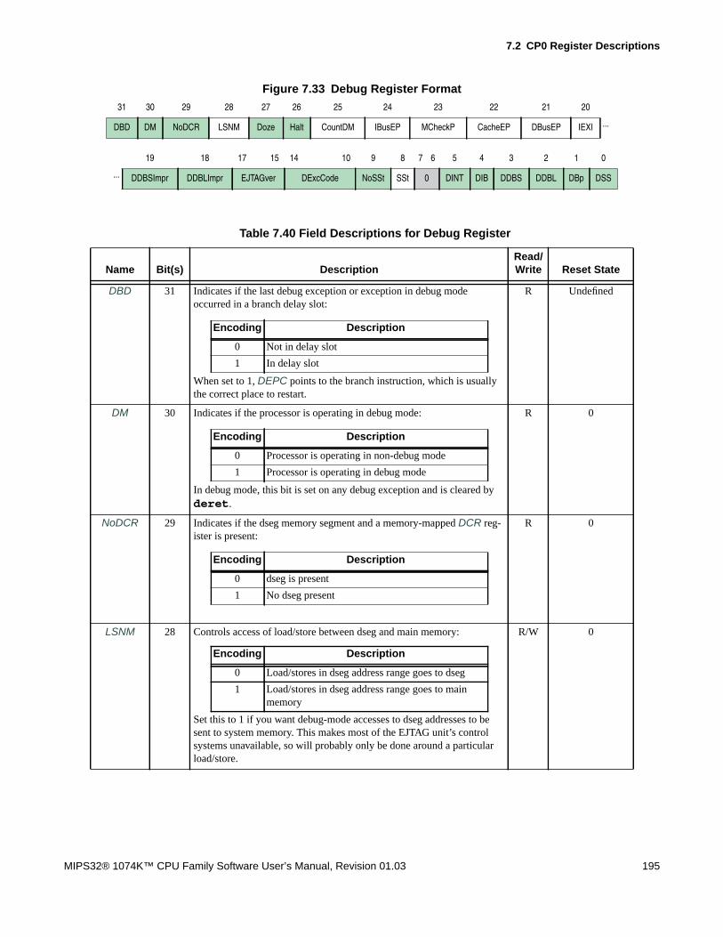
7.2 CP0 Register Descriptions
MIPS32® 1074K™ CPU Family Software User’s Manual, Revision 01.03 195
Figure 7.33 Debug Register Format31 30 29 28 27 26 25 24 23 22 21 20
DBD DM NoDCR LSNM Doze Halt CountDM IBusEP MCheckP CacheEP DBusEP IEXI ...
19 18 17 15 14 10 9 8 7 6 5 4 3 2 1 0
... DDBSImpr DDBLImpr EJTAGver DExcCode NoSSt SSt 0 DINT DIB DDBS DDBL DBp DSS
Table 7.40 Field Descriptions for Debug Register
Name Bit(s) DescriptionRead/Write Reset State
DBD 31 Indicates if the last debug exception or exception in debug modeoccurred in a branch delay slot:
When set to 1, DEPC points to the branch instruction, which is usuallythe correct place to restart.
R Undefined
DM 30 Indicates if the processor is operating in debug mode:
In debug mode, this bit is set on any debug exception and is cleared byderet.
R 0
NoDCR 29 Indicates if the dseg memory segment and a memory-mapped DCR reg-ister is present:
R 0
LSNM 28 Controls access of load/store between dseg and main memory:
Set this to 1 if you want debug-mode accesses to dseg addresses to besent to system memory. This makes most of the EJTAG unit’s controlsystems unavailable, so will probably only be done around a particularload/store.
R/W 0
Encoding Description
0 Not in delay slot
1 In delay slot
Encoding Description
0 Processor is operating in non-debug mode
1 Processor is operating in debug mode
Encoding Description
0 dseg is present
1 No dseg present
Encoding Description
0 Load/stores in dseg address range goes to dseg
1 Load/stores in dseg address range goes to mainmemory

CP0 Registers of the 1074K™ CPU
196 MIPS32® 1074K™ CPU Family Software User’s Manual, Revision 01.03
Doze 27 Indicates that the processor was in any kind of low power mode when adebug exception occurred:
Before the debug exception, CPU was in some kind of reduced powermode.
R Undefined
Halt 26 Indicates that the internal system bus clock was stopped when the debugexception occurred:.
Before the debug exception, the CPU was stopped — probably asleepfollowing a wait instruction.
R Undefined
CountDM 25 Controls or indicates the Count register behavior in debug mode: R/W 1
IBusEP 24 These "pending exception" flags remember exception events caused byinstructions run in debug mode, but which have not yet occurred becausethey are imprecise and DebugIEXI is set. Note that you can write a 1 toany of these at any time, so they survive writes to the whole Debug reg-ister; but a write of zero to a field is ignored.They remain set until DebugIEXI is cleared explicitly, or implicitly by aderet. If the deret clears the bit, the exception is taken and thepending bit cleared.IBusEP remembers a bus error on an instruction fetch. This exception isprecise on the 1074K CPU, so it can’t occur, and the field is always zero.MCheckP machine check condition (usually an illegal TLB update). Asabove, the machine check is always precise on the 1074K CPU, so this isalways zero.CacheEP remembers a cache parity error.DBusEP remembers a bus error on a data access.
R/W 0
MCheckP 23 R/W 0
CacheEP 22 R/W 0
DBusEP 21 R/W 0
IEXI 20 Set to 1 to defer imprecise exceptions. By default, this bit is set on entryto debug mode and cleared on exit. The deferred exception will returnwhen and if this bit is cleared, and until then you can observe the occur-rence of the imprecise exception in a “pending exception” flag(DebugIBusEP,MCheckP,CacheEP,DBusEP).
R/W 0
DDBSImpr 19 Imprecise store breakpoint. DEPC probably points to an instructionsome time later in the sequence than the store which triggered the break-point. The debugger or user (or both) have to cope as best they can.
R 0
Table 7.40 Field Descriptions for Debug Register (Continued)
Name Bit(s) DescriptionRead/Write Reset State
Encoding Description
0 Processor not in low power mode when debugexception occurred
1 Processor in low power mode when debug excep-tion occurred
Encoding Description
0 Internal system bus clock running
1 Internal system bus clock stopped
Encoding Description
0 Count register stopped in debug mode
1 Count register is running in debug mode

7.2 CP0 Register Descriptions
MIPS32® 1074K™ CPU Family Software User’s Manual, Revision 01.03 197
DDBLImpr 18 Imprecise load breakpoint. See description above of imprecise storebreakpoint.
R 0
EJTAGver 17:15 These read-only bits encode the revision of the EJTAG specification towhich this implementation conforms. On the 1074K CPU, the value is 3for version 3.1. The legal values are:
R 3
DExcCode 14:10 Indicates the cause of the latest exception in debug mode. Following ini-tial entry to debug mode, this field is undefined. The subsequent valuewill be one of those defined in CauseExcCode.
R Undefined
NoSSt 9 Indicates whether the single-step feature controllable by the SSt bit isavailable in this implementation. This read-only bit is always zero onMIPS Technologies’ cores because single-step is implemented.
R 0
SSt 8 Controls if debug single step exception is enabled. R/W 0
R 7..6 Reserved. Must be written as zeros; returns zeros on reads. R 0
DINT 5 Indicates that a debug interrupt exception (from EJTAG pin) occurred.Cleared on exception in debug mode.
R Undefined
DIB 4 Instruction breakpoint. R Undefined
DDBS 3 Indicates that a debug data break exception occurred on a store. Clearedon exception in debug mode.
R Undefined
DDBL 2 Indicates that a debug data break exception occurred on a load. Clearedon exception in debug mode.
R Undefined
Table 7.40 Field Descriptions for Debug Register (Continued)
Name Bit(s) DescriptionRead/Write Reset State
0 Version 2.0 and earlier
1 Version 2.5
2 Version 2.6
3 Version 3.1
Encoding Description
0 No debug interrupt exception
1 Debug interrupt exception
Encoding Description
0 No debug data exception on a store
1 Debug instruction exception on a store
Encoding Description
0 No debug data exception on a load
1 Debug instruction exception on a load

CP0 Registers of the 1074K™ CPU
198 MIPS32® 1074K™ CPU Family Software User’s Manual, Revision 01.03
7.2.32 Trace Control Register (CP0 Register 23, Select 1)
The TraceControl register configuration is shown below.
Figure 7.34 TraceControl Register Format
DBp 1 Indicates that a debug software breakpoint exception occurred. Clearedon exception in debug mode.
R Undefined
DSS 0 Indicates that a debug single-step exception occurred. Cleared on excep-tion in debug mode.
R Undefined
31 30 29 28 27 26 25 24 23 22 21 20 13 12 5 4 3 2 1 0
TS UT 0 Ineff TB IO D E K S U ASID_M ASID G TFCR TLSM TIM On
Table 7.41 TraceControl Register Field Descriptions
Fields
DescriptionRead /Write Reset StateName Bits
TS 31 The trace select bit is used to select between the hardware and thesoftware trace control bits. A value of zero selects the external hard-ware trace block signals, and a value of one selects the trace controlbits in the TraceControl register.
R/W 0
UT 30 This bit is deprecated since there are now two explicit trace regis-ters, UserTraceData1 and UserTraceData2. Previously this bitindicated the type of user-triggered trace record. A value of zeroimplies a user type 1, and a value of one implies a user type 2.
0 Undefined
R 29 Reserved for future use; Must be written as zero; returns zero onread.
0 0
Ineff 28 When set to 1, CPU-specific inefficiency tracing is enabled, andCPU-specific trace information is included in the trace stream. Theinefficiency code replaces an “NI” and is interpreted in the tracestream with an expanded InsComp (Instruction Completion Indica-tor). The InsComp is expanded from 3b to 4b for all trace formats.
R/W 0
Table 7.40 Field Descriptions for Debug Register (Continued)
Name Bit(s) DescriptionRead/Write Reset State
Encoding Description
0 No debug software breakpoint exception
1 Debug software breakpoint exception
Encoding Description
0 No debug single-step exception
1 Debug single-step exception

7.2 CP0 Register Descriptions
MIPS32® 1074K™ CPU Family Software User’s Manual, Revision 01.03 199
TB 27 Trace All Branch. When set to 1, this tells the processor to trace thePC value for all branches taken, not just the ones whose branch tar-get address is statically unpredictable.
R/W Undefined
IO 26 Inhibit Overflow. This signal is used to indicate to the CPU tracelogic that slow but complete tracing is desired. Hence, the CPU trac-ing logic must not allow a FIFO overflow and discard trace data.This is achieved by stalling the pipeline when the FIFO is nearlyfull, so that no trace records are ever lost.
R/W Undefined
D 25 When set to one, this enables tracing in Debug Mode. For trace to beenabled in Debug mode, the On bit must also be one, and either theG bit must be one, or the current process ASID must match theASID field in this register.When set to zero, trace is disabled in Debug Mode, regardless of thesetting other bits.
R/W Undefined
E 24 When set to one, enables tracing in Exception Mode. For trace to beenabled in Exception mode, the On bit must be one, and either the Gbit must be one, or the current process ASID must match the ASIDfield in this register.When set to zero, trace is disabled in Exception Mode, regardless ofthe setting of other bits.
R/W Undefined
K 23 When set to one, enables tracing in Kernel Mode. For trace to beenabled in Kernel mode, the On bit must be one, and either the G bitmust be one, or the current process ASID must match the ASID fieldin this register.When set to zero, trace is disabled in Kernel Mode, regardless of thesetting other bits.
R/W Undefined
S 22 When set to one, this enables tracing in Supervisor Mode.For traceto be enabled in Supervisor mode, the On bit must be one, and eitherthe G bit must be one, or the current process ASID must match theASID field in this register.When set to zero, trace is disabled in Supervisor Mode, regardless ofother bits.If the processor does not implement Supervisor Mode, this bit isignored on write and returns zero on read.
R/W Undefined
U 21 When set to one, enables tracing in User Mode. For trace to beenabled in User mode, the On bit must be one, and either the G bitmust be one, or the current process ASID must match the ASID fieldin this register.When set to zero, trace is disabled in User Mode, regardless of thesetting of other bits.
R/W Undefined
ASID_M 20:13 This is a mask value applied to the ASID comparison (done whenthe G bit is zero). A “1” in any bit in this field inhibits the corre-sponding ASID bit from participating in the match. As such, a valueof zero in this field compares all bits of ASID. Note that the abilityto mask the ASID value is not available in the hardware signal bit; itis only available via the software control register.If the processor does not implement the standard TLB-based MMU,this field is ignored on writes and returns zero on reads.
R/W Undefined
Table 7.41 TraceControl Register Field Descriptions (Continued)
Fields
DescriptionRead /Write Reset StateName Bits

CP0 Registers of the 1074K™ CPU
200 MIPS32® 1074K™ CPU Family Software User’s Manual, Revision 01.03
7.2.33 Trace Control2 Register (CP0 Register 23, Select 2)
The TraceControl2 register provides additional control and status information. Note that some fields in theTraceControl2 register are read-only, but have a reset state of “Undefined”. This is because these values are loadedfrom the Trace Control Block (TCB) (see Section 11.10 “Trace Control Block (TCB) Registers (HardwareControl)”). As such, these fields in the TraceControl2 register will not have valid values until the TCB asserts thesevalues.
This register is only implemented if the MIPS Trace capability is present.
Figure 7.35 TraceControl2 Register Format
ASID 12:5 The ASID field to match when the G bit is zero. When the G bit isone, this field is ignored.If the processor does not implement the standard TLB-based MMU,this field is ignored on writes and returns zero on reads.
R/W Undefined
G 4 When set, this implies that tracing is to be enabled for all processes,provided that other enabling functions (like U, S, etc.,) are also true.If the processor does not implement the standard TLB-based MMU,this field is ignored on writes and returns 1 on reads. This causes allmatch equations to work correctly in the absence of an ASID.
R/W Undefined
TFCR 3 When set, indicates to the PDtrace interface that the optional Fcr bitmust be traced in the appropriate trace formats. If PC tracing is dis-abled, the full PC of the function call (or return) instruction mustalso be traced. Note that function call/return information is onlytraced if tracing is actually enabled for the current mode.
R/W Undefined
TLSM 2 When set, this indicates to the PDtrace interface that informationabout data cache misses should be traced. If PC, load/store address,and data tracing are disabled (see the TraceControl2Mode field), thefull PC and load/store address are traced for data cache misses. Ifload/store data tracing is enabled, the LSm bit must be traced in theappropriate trace format. Note that data cache miss information isonly traced if tracing is actually enabled for the current mode.
R/W Undefined
TIM 1 When set, this indicates to the PDtrace interface that the optional Imbit must be traced in the appropriate trace formats. If PC tracing isdisabled, the full PC of the instruction that missed in the I-cachemust be traced. Note that instruction cache miss information is onlytraced if tracing is actually enabled in the current mode.
R/W Undefined
On 0 This is the master trace enable switch in software control. Whenzero, tracing is always disabled. When set to one, tracing is enabledwhenever the other enabling functions are also true.
R/W 0
31 30 29 28 21 20 19 12 11 7 6 5 4 3 2 1 0
SyPExt CPUIdV CPUId TCV TCNum Mode ValidModes TBI TBU SyP
Table 7.41 TraceControl Register Field Descriptions (Continued)
Fields
DescriptionRead /Write Reset StateName Bits

7.2 CP0 Register Descriptions
MIPS32® 1074K™ CPU Family Software User’s Manual, Revision 01.03 201
Table 7.42 TraceControl2 Register Field Descriptions
Fields
DescriptionRead /Write Reset StateName Bits
SyPExt 31:30 Extension to the SyP (sync period) field for implementations thatneed higher numbers of cycles between synchronization events.The value of SyP is extended by assuming that these two bits arejuxtaposed to the left of the three bits of SyP (SypExtSyP). Whenonly SyP was used to specify the synchronization period, the valuewas 2x, where x was computed from SyP by adding 5 to the actualvalue represented by the bits. A similar formula is applied to the 5bits just obtained by the juxtaposition of SyPExt and SyP. Sync
period values greater than 231 are UNPREDICTABLE. That is allvalues greater than 11010 (26+5=31) are UNPREDICTABLE. With
SyPExt bits, a sync period range of 25 to 231 cycles can be obtained.
R/W 0
CPUIdV 29 When set, this bit specifies the VPE defined in CPUId must betraced. Otherwise, instructions from all VPEs are traced when otherconditions for tracing are valid. This bit is ignored if TCV isasserted.
R/W 0
CPUId 28:21 This field specifies the number of the VPE to trace when CPUIdV isset.
R/W 0
TCV 20 When set, the TCNum field specifies the number of the TC thatmust be traced. Otherwise, instructions from all TCs are traced whenother conditions for tracing are valid.
R/W 0
TCNum 19:12 Specifies the TC to trace when TCV is set. The right-most bits onlyare used.
R/W 0
Mode 11:7 When tracing is turned on, this signal specifies what information isto be traced by the CPU. It uses 5 bits, where each bit turns on trac-ing of a specific tracing mode when that bit value is a 1. If the corre-sponding bit is 0, then the Trace Value shown in column two is nottraced by the processor. The table shows what trace value is turnedon:
R/W Undefined
ValidModes 6:5 This field specifies the subset of tracing that is supported by the pro-cessor.
R Preset
Bit Trace the Following
7 PC
8 Load address
9 Store address
10 Load data
11 Store data
Encoding Meaning
00 PC tracing only
01 PC and load and store address tracing only
10 PC, load and store address, and load and store data
11 Reserved

CP0 Registers of the 1074K™ CPU
202 MIPS32® 1074K™ CPU Family Software User’s Manual, Revision 01.03
7.2.34 User Trace Data1 Register (CP0 Register 23, Select 3) and User Trace Data2Register (CP0 Register 24, Select 3)
A software write to any bits in the UserTraceData1 register or UserTraceData2 register will trigger a trace record tobe written with a type indicator TU1 or TU2 respectively.
These register are only implemented if the MIPS Trace capability is present.
TBI 4 This bit indicates how many trace buffers are implemented by theTCB, as follows:
R Undefined
TBU 3 This bit denotes to which trace buffer the trace is currently beingwritten and is used to select the appropriate interpretation of theTraceControl2SyP field.
This bit is loaded from TCBCONTROLBOfC.
R Undefined
SyP 2:0 The period (in cycles) to which the internal synchronization counteris reset when tracing is started, or when the synchronization counterhas overflowed.
This field is loaded from TCBCONTROLASyP.
R Undefined
Table 7.42 TraceControl2 Register Field Descriptions (Continued)
Fields
DescriptionRead /Write Reset StateName Bits
Encoding Meaning
0 Only one trace buffer is implemented, and the TBUbit of this register indicates which trace buffer isimplemented
1 Both on-chip and off-chip trace buffers are imple-mented by the TCB and the TBU bit of this registerindicates to which trace buffer the traces is cur-rently written.
Encoding Meaning
0 Trace data is being sent to an on-chip trace buffer
1 Trace Data is being sent to an off-chip trace buffer
SyP Sync Period
000 25
001 26
010 27
011 28
100 29
101 210
110 211
111 212

7.2 CP0 Register Descriptions
MIPS32® 1074K™ CPU Family Software User’s Manual, Revision 01.03 203
Figure 7.36 User Trace Data1 / User Trace Data2 Register Format
7.2.35 TraceIBPC Register (CP0 Register 23, Select 4)
The TraceIBPC register is used to control start and stop of tracing using an EJTAG Instruction Hardware breakpoint.The Instruction Hardware breakpoint would then be set as a trigger source and optionally also as a Debug exceptionbreakpoint.
This register is only implemented if both Hardware breakpoints and the MIPS Trace capability are present.
Figure 7.37 TraceIBPC Register Format
31 0
Data
Table 7.43 UserTraceData1 / UserTraceData2 Register Field Descriptions
Fields
DescriptionRead /Write Reset StateName Bits
Data 31:0 Software readable/writable data. When written, this triggers a userformat trace record out of the PDtrace interface that transmits theData field to trace memory.
R/W 0
31 30 29 28 27 12 11 9 8 6 5 3 2 0
0 PCT IE 0 IBPC3 IBPC2 IBPC1 IBPC0
Table 7.44 TraceIBPC Register Field Descriptions
Fields
DescriptionRead /Write Reset StateName Bits
0 31:30,27:12
Reserved for future implementations. R 0
PCT 29 Used to specify whether a performance counter trigger signal is gen-erated when an EJTAG instruction breakpoint match occurs:
R/W 0
IE 28 Used to specify whether or not the trigger signal from EJTAGinstruction breakpoint should trigger tracing functions:
R/W 0
Encoding Meaning
0 Disables performance counter trigger signal frominstruction breakpoints
1 Enables performance trigger signals from instruc-tion breakpoints
Encoding Meaning
0 Disables trigger signals from instruction break-points
1 Enables trigger signals from instruction break-points

CP0 Registers of the 1074K™ CPU
204 MIPS32® 1074K™ CPU Family Software User’s Manual, Revision 01.03
7.2.36 TraceDBPC Register (CP0 Register 23, Select 5)
The TraceDBPC register is used to control start and stop of tracing using an EJTAG Data Hardware breakpoint. TheData Hardware breakpoint would then be set as a trigger source and optionally also as a Debug exception breakpoint.
This register is only implemented if both Hardware breakpoints and the MIPS Trace capability are present.
Figure 7.38 TraceDBPC Register Format
IBPCn 3n+2:3n The three bits are decoded to enable different tracing modes. Table7.46 shows the possible interpretations. Each set of 3 bits representsthe encoding for the instruction breakpoint n in the EJTAG imple-mentation, if it exists. If the breakpoint does not exist, then the bitsare reserved, read as zero, and writes are ignored.
R/W 0
31 30 29 28 27 6 5 3 2 0
0 PCT DE 0 DBPC1 DBPC0
Table 7.45 TraceDBPC Register Field Descriptions
Fields
DescriptionRead /Write Reset StateName Bits
0 31:30,27:6
Reserved for future implementations. R 0/1
PCT 29 Used to specify whether a performance counter trigger signal is gen-erated when an EJTAG data breakpoint match occurs:
R/W 0
DE 28 Used to specify whether the trigger signal from EJTAG data break-point should trigger tracing functions:
R/W 0
DBPCn 3n+2:3n The three bits are decoded to enable different tracing modes. Table7.46 shows the possible interpretations. Each set of 3 bits representsthe encoding for the data breakpoint n in the EJTAG implementa-tion, if it exists. If the breakpoint does not exist then the bits arereserved, read as zero and writes are ignored.
R/W 0
Table 7.44 TraceIBPC Register Field Descriptions (Continued)
Fields
DescriptionRead /Write Reset StateName Bits
Encoding Meaning
0 Disables performance counter trigger signal fromdata breakpoints
1 Enables performance trigger signals from databreakpoints
Encoding Meaning
0 Disables trigger signals from data breakpoints
1 Enables trigger signals from data breakpoints
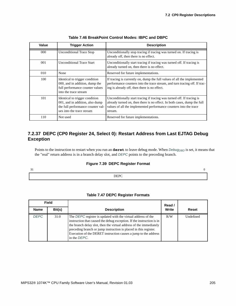
7.2 CP0 Register Descriptions
MIPS32® 1074K™ CPU Family Software User’s Manual, Revision 01.03 205
7.2.37 DEPC (CP0 Register 24, Select 0): Restart Address from Last EJTAG DebugException
Points to the instruction to restart when you run an deret to leave debug mode. When DebugDBD is set, it means thatthe "real" return address is in a branch delay slot, and DEPC points to the preceding branch.
Figure 7.39 DEPC Register Format
Table 7.46 BreakPoint Control Modes: IBPC and DBPC
Value Trigger Action Description
000 Unconditional Trace Stop Unconditionally stop tracing if tracing was turned on. If tracing isalready off, then there is no effect.
001 Unconditional Trace Start Unconditionally start tracing if tracing was turned off. If tracing isalready turned on, then there is no effect.
010 None Reserved for future implementations.
100 Identical to trigger condition000, and in addition, dump thefull performance counter valuesinto the trace stream
If tracing is currently on, dump the full values of all the implementedperformance counters into the trace stream, and turn tracing off. If trac-ing is already off, then there is no effect.
101 Identical to trigger condition001, and in addition, also dumpthe full performance counter val-ues into the trace stream
Unconditionally start tracing if tracing was turned off. If tracing isalready turned on, then there is no effect. In both cases, dump the fullvalues of all the implemented performance counters into the tracestream.
110 Not used Reserved for future implementations.
31 0
DEPC
Table 7.47 DEPC Register Formats
Field
DescriptionRead /Write ResetName Bit(s)
DEPC 31:0 The DEPC register is updated with the virtual address of theinstruction that caused the debug exception. If the instruction is inthe branch delay slot, then the virtual address of the immediatelypreceding branch or jump instruction is placed in this register.Execution of the DERET instruction causes a jump to the addressin the DEPC.
R/W Undefined

CP0 Registers of the 1074K™ CPU
206 MIPS32® 1074K™ CPU Family Software User’s Manual, Revision 01.03
7.2.38 Trace Control3 Register (CP0 Register 24, Select 2)
The TraceControl3 register provides additional control and status information. Note that some fields in theTraceControl3 register are read-only, but have a reset state of “Undefined”. This is because these values are loadedfrom the Trace Control Block (TCB) (see Section 11.10 “Trace Control Block (TCB) Registers (HardwareControl)”). As such, these fields in the TraceControl3 register will not have valid values until the TCB asserts thesevalues.
This register is only implemented if the MIPS Trace capability is present.
Figure 7.40 TraceControl3 Register Format31 14 13 12 11 10 9 8 7 2 1 0
0 PeCOvf PeCFCR PeCBP PeCSync PeCE PeC 0 TRPAD FDT
Table 7.48 TraceControl3 Register Field Descriptions
Fields
DescriptionRead /Write Reset StateName Bits
0 31:14 Reserved for future implementations. R 0
PeCOvf 13 Trace performance counters when one of the performance countersoverflows its count value. Enabled when set to 1.
R/W 0
PeCFCR 12 Trace performance counters on function call/return or on an excep-tion handler entry. Enabled when set to 1.
R/W 0
PeCBP 11 Trace performance counters on hardware breakpoint match trigger.Enabled when set to 1.
R/W 0
PeCSync 10 Trace performance counters on synchronization counter expiration.Enabled when set to 1.
R/W 0
PeCE 9 Performance counter tracing enable. When set to 0, the tracing out ofperformance counter values as specified is disabled. To enable, thisbit must be set to 1. This bit is used under software control. Whentrace is controlled by an external probe, this enabling is done viaTraceControl3PeCE.
R/W 0
PeC 8 Specifies whether or not Performance Control Tracing is imple-mented. This is an optional feature that may be omitted by imple-mentation choice. Implemented when set to 1.
R/W 0
TrIDLE 2 Trace Unit Idle. This bit indicates if the trace hardware is currentlyidle (not processing any data). This can be useful when switchingcontrol of trace from hardware to software and vice versa. The bit isread-only and updated by the trace hardware.
R/W 0
TRPAD 1 Trace RAM Access Disable. Disables program software access tothe on-chip trace RAM using load/store instructions. This bit isloaded from TCBCONTROLBTRPAD.
R/W 0
FDT 0 Filtered Data Trace Mode Enable. When the bit is 0, this mode isdisabled. When set to 1, this mode is enabled.
R/W 0

7.2 CP0 Register Descriptions
MIPS32® 1074K™ CPU Family Software User’s Manual, Revision 01.03 207
7.2.39 PerfCtl0-3 (CP0 Register 25, Select 0, 2, 4, 6): Performance Counter Control
Cores in the 1074K family provide four performance counters that provide the capability to count events or cycles foruse in performance analysis. Each performance counter consists of a pair of registers: a 32-bit control register(PerfCtl) and a 32-bit counter register (PerfCnt) .
Performance counters can be configured to count implementation-dependent events or cycles under a specified set ofconditions that are determined by the performance counter’s control register. The counter register increments oncefor each enabled event; when the most-significant bit of the counter register is a one (the counter overflows), and thecounter is enabled, the performance counter optionally requests an interrupt.
The IE flag in the performance counter control register is used to enable an interrupt to be signalled when bit 31 of thecorresponding counter overflows. The OR of all the performance counter register interrupts becomes the CPU outputSI_PCI, which is typically fed back into an interrupt input, conventionally identified by IntCtlIPPCI. However, systemsusing more sophisticated interrupt controllers may feed the performance counter interrupt into the interrupt controller(refer to Section 6.3.1.3, "External Interrupt Controller Mode").
Figure 7.41 PerfCtl0-3 Register Format31 30 16 15 14 12 11 5 4 3 2 1 0
M 0 PCTD 0 Event IE U S K EXL
Table 7.49 Field Descriptions for PerfCtl0-3 Register
Name Bit(s) DescriptionRead/Write Reset State
M 31 Set to 1 if there is another PerfCtl register after this one. This field is setfor PerfCtl0-2 and cleared on PerfCtl3.
R X
PCTD 15 Performance Counter Trace Disable. Setting this bit will prevent the trac-ing of data from this performance counter when performance countertrace mode in PDTrace is enabled.
R/W Undefined
Event 11:5 Determines which event to count. Available events are listed in Table7.50, "Performance Counter Events and Codes".
R/W Undefined
IE 4 Set to cause an interrupt when the counter overflows into bit 31. This caneither be used to implement an extended count or (by presetting thecounter appropriately) to notify software after a certain number of eventshave occurred.
R/W 0
U 3 Count events in User mode, Supervisor mode, Kernel mode, and Excep-tion mode (i.e., when StatusEXL is set) respectively. Set multiple bits tocount in all cases.
R/W Undefined
S 2 R/W Undefined
K 1 R/W Undefined
EXL 0 R/W Undefined
Table 7.50 Performance Counter Events and Codes
EventNo Counter0/2 Counter1/3
0 Cycles
1 Instructions graduated

CP0 Registers of the 1074K™ CPU
208 MIPS32® 1074K™ CPU Family Software User’s Manual, Revision 01.03
2 jr $31 (return) instructions whose target is pre-dicted
jr $31 (return) predicted but guessed wrong
3 Cycles where no instruction is fetched because it hasno “next address” candidate. This includes stalls dueto register indirect jumps such as jr, stalls follow-ing a wait or eret and stalls dues to excep-tions from instruction fetch
jr $31 (return) instructions fetched and not pre-dicted using RPS
4 ITLB accesses. ITLB misses, which result in a JTLB access.
5 Reserved JTLB instruction access misses (will lead to anexception)
6 Instruction Cache accesses. 1074K cores have a 128-bit connection to the I-cache and fetch 4 instructionsevery access. This counts every such access, includ-ing accesses for instructions which are eventuallydiscarded. For example, following a branch which isincorrectly predicted, the 1074K CPU will continueto fetch instructions, which will eventually getthrown away.
Instruction cache misses. Includes misses resultingfrom fetch-ahead and speculation.
7 Cycles where no instruction is fetched because wemissed in the I-cache.
Reserved
8 Cycles where no instruction is fetched because weare waiting for an I-fetch from uncached memory.
PDTrace back stalls
9 Number of times the instruction fetch pipeline isflushed and replayed because the IFU buffers are fulland unable to accept any instructions.
Valid fetch slots killed due to taken branches/jumpsor stalling instructions
10 Store misses transitioning to I->M or S->M Load misses transitioning to I->S or I->E
11 Table 7.36, "Field Descriptions for Config6Register"
12 • Intervention hits
13 Cycles where no instructions are brought into theIDU because the ALU instruction candidate pool isfull.
Cycles where no instructions are brought into theIDU because the AGEN instruction candidate pool isfull.
14 Cycles where no instructions can be added to theissue pool because we have run out of ALU comple-tion buffers (CB’s).
Cycles where no instructions can be added to theissue pool because we have run out of AGEN com-pletion buffers (CB’s).
15 Cycles where no instructions can be added to theissue pool, because we have used all the FIFO entriesin the CLDQ, which keep track of data coming backfrom the FPU.
Cycles where no instructions can be added to theissue pool, because we have filled the “in order”FIFO used for coprocessor 1 instructions (IOIQ).
Table 7.50 Performance Counter Events and Codes (Continued)
EventNo Counter0/2 Counter1/3

7.2 CP0 Register Descriptions
MIPS32® 1074K™ CPU Family Software User’s Manual, Revision 01.03 209
16 Cycles with no ALU-pipe issue: no instructionsavailable.
Cycles with no AGEN-pipe issue: no instructionsavailable.
17 Cycles with no ALU-pipe issue: we have instruc-tions, but operands not ready.
Cycles with no AGEN-pipe issue: we have instruc-tions, but operands not ready.
18 Cycles with no ALU-pipe issue: we have instruc-tions, but some resource is unavailable. Thisincludes:• Operands are not ready (same as event 17)• div in progress inhibits MDU instructions• CorExtend resource limitation.
Cycles with no AGEN-pipe issue: we have instruc-tions, but some resource is unavailable. Thisincludes:• Operands not ready (same as event 17)• Non-issued stores blocking ready to issue loadsis-
sued cacheops blocking ready to issue loads
19 ALU-pipe bubble issued. This resulting empty pipestage guarantees that some resource will be unusedfor a cycle, sometime soon. Used, for example, toguarantee an opportunity to write mfc1 data into aCB.•
AGEN-pipe bubble issued. This resulting empty pipestage guarantees that some resource will be unusedfor a cycle, sometime soon. Used, for example, toallow access to the data cache for refill or eviction.
•
20 Cycles when only one instruction is issued. Cycles when two instructions are issued (one ALU,one AGEN).
21 Cycles when instructions are issued out of order intothe ALU pipe. i.e. instruction issued is not the oldestin the pool.
Cycles when instructions are issued out of order intothe AGEN pipe. i.e. instruction issued is not the old-est in the pool.
22 Graduated JAR/JALR.HB D-cache line refill (not LD/ST misses)
23 Cacheable loads - Counts all accesses to the D-cachecaused by load instructions. This count includesinstructions that do not graduate.
All D-cache accesses (loads, stores, prefetch,cacheop etc.). This count includes instructions thatdo not graduate.
24 D-cache writebacks D-cache misses. This count is per instruction at grad-uation and includes load, store, prefetch, synciand address based cacheops.
25 JTLB d-side (data side as opposed to instructionside) accesses
JTLB translation fails on d-side (data side asopposed to instruction side) accesses. This countincludes instructions that do not graduate.
26 Load/store instruction redirects, which happen whenthe load/store follows too closely on a possiblymatching cacheop.
The 1074K CPU’s D-cache has an auxiliary virtualtag, used to pick the right line early. When (occasion-ally) the physical tag match and virtual tag match donot line up, it is treated as a cache miss - in process-ing the “miss” the virtual tag is corrected for futureaccesses. This event counts those bogus misses.
27 •
28 L2 cache writebacks L2 cache accesses
29 L2 cache misses L2 cache miss cycles
30 Cycles Fill Store Buffer(FSB) are full and cause apipe stall
Cycles Fill Store Buffer(FSB) > 1/2 full
31 Cycles Load Data Queue (LDQ) are full and cause apipe stall
Cycles Load Data Queue(LDQ) > 1/2 full
Table 7.50 Performance Counter Events and Codes (Continued)
EventNo Counter0/2 Counter1/3

CP0 Registers of the 1074K™ CPU
210 MIPS32® 1074K™ CPU Family Software User’s Manual, Revision 01.03
32 Cycles Writeback Buffer(WBB) are full and cause apipe stall
Cycles Writeback Buffer(WBB) > 1/2 full
33 Count of requests that will receive data from the CM Request latency to first DW of data from the CM
34 Invalidate intervention hits All invalidate interventions
35 Replays following optimistic issue of instructiondependent on load which missed. Counted only whenthe dependent instruction graduates.
Floating Point Load instructions graduated.
36 jr (not $31) instructions graduated. jr $31 mispredicted at graduation
37 Integer Branch instructions graduated Floating Point Branch instructions graduated
38 Branch likely instructions graduated Mispredicted Branch likely instructions graduated
39 Conditional branches graduated Mispredicted Conditional branches graduated
40 Integer instructions graduated (includes nop,ssnop, ehb as well as all arithmetic, logic,shift and extract type operations).
Floating Point instructions graduated (but not count-ing Floating Point load/store)
41 Loads graduated (includes Floating Point) Stores graduated (includes Floating Point). Of scinstructions, only successful ones are counted.
42 j/jal graduated MIPS16e instructions graduated
43 no-ops graduated - included (sll, nop,ssnop, ehb).
integer multiply/divides graduated
44 DSP instructions graduated ALU-DSP instructions graduated, result was satu-rated
45 DSP branch instructions graduated MDU-DSP instructions graduated, result was satu-rated.
46 Uncached loads graduated. Uncached stores graduated.
47 Writebacks due to evictions Writebacks due to any reason
48 Count of all invalidates (M,E,S)->I Count of transitions from (I,S)->E
49 EJTAG instruction triggers EJTAG data triggers
50 CP1 branches mispredicted. Reserved
51 sc instructions graduated. sc instructions failed.
52 prefetch instructions graduatedat the top ofLSGB.
prefetch instructions which did nothing,because they hit in the cache.
53 Cycles where no instructions graduated Load misses graduated. Includes Floating PointLoads.
54 Cycles where one instruction graduated Cycles where two instructions graduated
55 GFifo blocked cycles Floating point stores graduated
Table 7.50 Performance Counter Events and Codes (Continued)
EventNo Counter0/2 Counter1/3

7.2 CP0 Register Descriptions
MIPS32® 1074K™ CPU Family Software User’s Manual, Revision 01.03 211
56 GFifo blocked due to TLB or Cacheop Number of cycles no instructions graduated from thetime the pipe was flushed because of a replay untilthe first new instruction graduates. This is an indica-tor graduation bandwidth loss due to replay. Oftentimes this replay is a result of event 25 and thereforean indicator of bandwidth lost due to cache miss.
57 Slot 0 mispredicted branch instruction graduationcycles without the delayslo
Cycles waiting for delayslot to graduate on a mispre-dicted branch
58 Exceptions taken Replays initiated from graduation
59 Implementation-specific CorExtend event. The inte-grator of this CPU may connect the CPU pinUDI_perfcnt_event to an event to be counted. Thisis intended for use with the CorExtend interface.
Reserved
60 State transition from S->M (coherent and non-coh) State transitions from (M,E)->S
61 Request latency to self-intervention Count of requests that will receive self-intervention
62 Implementation-specific DSPRAM event. The inte-grator of this CPU may connect the pinSP_prf_c13_e62_xx to the event to be counted
63 L2 single-bit errors detected All interventions
64 SI_Event[0] - Implementation-specific system event.The integrator of this CPU may connect the CPU pinSI_PCEvent[0] to an event to be counted
SI_Event[1] - Implementation-specific system event.The integrator of this CPU may connect the CPU pinSI_PCEvent[1] to an event to be counted
65 SI_Event[2] - Implementation-specific system event.The integrator of this CPU may connect the CPU pinSI_PCEvent[2] to an event to be counted
SI_Event[3] - Implementation-specific system event.The integrator of this CPU may connect the CPU pinSI_PCEvent[3] to an event to be counted
66 SI_Event[4] - Implementation-specific system event.The integrator of this CPU may connect the CPU pinSI_PCEvent[4] to an event to be counted
SI_Event[5] - Implementation-specific system event.The integrator of this CPU may connect the CPU pinSI_PCEvent[5] to an event to be counted
67 SI_Event[6] - Implementation-specific system event.The integrator of this CPU may connect the CPU pinSI_PCEvent[6] to an event to be counted
SI_Event[7] - Implementation-specific system event.The integrator of this CPU may connect the CPU pinSI_PCEvent[7] to an event to be counted
68 All OCP requests accepted All OCP cacheable requests accepted
69 OCP read requests accepted OCP cacheable read requests accepted
70 OCP write requests accepted OCP cacheable write requests accepted
71 Reserved OCP write data sent
72 Reserved OCP read data received
73 OCP Intervention write data stalled (valid but notaccepted)
OCP Intervention write data valid (accepted or not)
74 Cycles Fill Store Buffer(FSB) < 1/4 full Cycles Fill Store Buffer(FSB) 1/4 to 1/2 full
75 Cycles Load Data Queue (LDQ) < 1/4 full Cycles Load Data Queue (LDQ) 1/4 to 1/2 full
76 Cycles Writeback Buffer(WBB) < 1/4 full Cycles Writeback Buffer(WBB) 1/4 to 1/2 full
77-127 Reserved Reserved
Table 7.50 Performance Counter Events and Codes (Continued)
EventNo Counter0/2 Counter1/3

CP0 Registers of the 1074K™ CPU
212 MIPS32® 1074K™ CPU Family Software User’s Manual, Revision 01.03
7.2.40 PerfCnt0-3 (CP0 Register 25, Select 1, 3, 5, 7): Performance Counters
General purpose event counters, which operate as directed by PerfCtl0-3.
Figure 7.42 Performance Counter Count Register
7.2.41 ErrCtl (CP0 Register 26, Select 0): Software Parity Control and Test Modes forCache RAM Arrays
Most of the fields of this register are for test software only. The MIPS32 Architecture defines this register as imple-mentation-dependent, but most CPUs put the parity-enable control in the top bit. So running OS software is welladvised to set this register to 0x8000.0000 to enable cache parity checking, or to zero to disable parity checking.
31 0
Counter
Table 7.51 Performance Counter Count Register Field Descriptions
Fields
DescriptionRead /Write Reset StateName Bits
Counter 31:0 Counter R/W Undefined
31 0
Counter
31 30 29 28 27 26 25 24 23 22 21 20 19 18 12 11 4 3 0
PE PO WST SPR PCO ITC LBE WABE L2P, L2EccEnable PCD DYT SE FE 0 PI PD
Table 7.52 Field Descriptions for ErrCtl Register
Name Bit(s) DescriptionRead/Write Reset State
PE 31 1 to enable cache parity checking. Hard-wired to zero if parity isn’timplemented.
R/W 0
PO 30 Parity Overwrite. Set 1 to set the parity bit regardless of parity computa-tion, which is only for diagnostic/test purposes.After setting this bit you can use cache IndexStoreTag to setthe cache data parity to the value currently in PI (for I-cache) or PD (forD-cache), while the tag parity is forcefully set from ITagLoP/DTagLoP.
R/W 0
WST 29 Write to 1 for test mode for cache IndexLoadTag/cache IndexStoreTag instructions, which then read/write thecache’s internal way-selection RAM instead of the cache tags.
R/W 0
SPR 28 Scratchpad RAM. When set, index-type cache instructions work on thescratchpad/DSPRAM/ISPRAM, if fitted.
R/W 0
PCO 27 Precode override. Used for diagnostic/test of the I-cache. When this bit isset, then the precode values in the ITagHi register are used instead of thehardware generated precode values. This applies to index store datacacheop operation.
R/W 0
ITC 26 Reserved R/W Undefined

7.2 CP0 Register Descriptions
MIPS32® 1074K™ CPU Family Software User’s Manual, Revision 01.03 213
7.2.42 CacheErr (CP0 Register 27, Select 0): Cache Parity Exception Status
Read-only register used to analyze the details of a parity error.
Figure 7.43 CacheErr Register Format
LBE 25 Indicates whether a bus error (the last one, if there’s been more than one)was triggered by a load or a write-allocate respectively. A write-allocateis where a cacheable write has missed in the cache, and the cache hasread the line from memory.Where both a load and write-allocate are waiting on the same cache-linerefill, both could be set. These bits are "sticky", remaining set untilexplicitly written zero.
R/W0 Undefined
WABE 24 R/W0 Undefined
L2P,L2EccEnable
23 L2 Present, L2EccEnable: Indicates whether ECC is enabled on theL2Cache if present.• 0: L2Presetnt & L2EccEnable = 0• 1: L2Present & L2EccEnable = 1
R/W 0
DYT 21 Set 1 to arrange that cache load/store data operations work on the"dirty array" — the slice of cache memory which holds the "dirty"/"stored-into" bits.
R/W 0
PCD 22 Precode Disable. When set, cache IndexStoreTag instructionsdo not update the corresponding precode field and precode parity in theinstruction cache tag array.
R/W 0
SE 20 Indicates that a second cache error was detected before the first error wasprocessed. This is an unrecoverable error. This bit is set when a cacheerror is detected while the FE bit is set. This bit is cleared on reset orwhen a cache error is detected with FE cleared.
R 0
FE 19 Indicates that this is the first cache error and therefore potentially recov-erable. Error handling software should clear this bit when the error hasbeen processed. This bit is cleared on reset. Refer to SE bit descriptionfor implications of this bit. Note that software can only write a 0 to thisbit. A write value of 1 will not have any effect.
R/W 0
PI 11:4 Parity bits being read/written to caches (I- and D-cache respectively),when PO is set.
R/W
PD 3:0 R/W
31 30 29 28 27 26 25 24 23 22 21 19 18 17 16 0
ER EC ED ET ES EE EB EF SP EW Way DR Index
Table 7.53 Field Descriptions for CacheErr Register
Name Bit(s) DescriptionRead/Write Reset State
ER 31 This bit reads 1 if the error was on a L1 data cache access and reads 0otherwise. For errors caused by L1 I-fetch or L2 or higher level cacheaccesses, this bit will read 0.
R Undefined
EC 30 Reads 0 if L1 cache errors and 1 for higher-level caches. R Undefined
Table 7.52 Field Descriptions for ErrCtl Register (Continued)
Name Bit(s) DescriptionRead/Write Reset State

CP0 Registers of the 1074K™ CPU
214 MIPS32® 1074K™ CPU Family Software User’s Manual, Revision 01.03
ED 29 Set for errors in data field and tag field respectively for Instruction cache. R Undefined
ET 28 R Undefined
ED:ET 29:28 For D-cache, these bits encode the array in which an error was detected. R Undefined
ES 27 Error source. Reads 0 if error was caused by internal processor and 1 ifexternal snoop request.
R Undefined
EE 26 Error external: Indicates that a parity error was seen on a coherent L1cache in another CPU.
R Undefined
EB/EM 25 • If EC equals 0 indicating an error in the L1 cache, this bit is EB, indi-cating Error in Both caches. If data and instruction-fetch error arereported on the same instruction, it is unrecoverable. If so, the rest ofthe register reports on the instruction-fetch error.
• If EC equals 1 indicating an error in the L2 or higher cache, this bit isEM, indicating Error in Multiple locations.
R Undefined
EF 24 Unrecoverable (fatal) error (other than the EB type above). Some parityerrors can be fixed by invalidating the cache line and relying on gooddata from memory. But if this bit is set, all is lost... It’s one of the follow-ing:7.53.1 Dirty parity error in dirty victim7.53.1 Line being displaced from cache ("victim") has a tag parity error,
so we don’t know whether to write it back, or whether the writebacklocation (which needs a correct tag) would be correct.
7.53.2 The victim’s tag indicates it has been written by the CPU since itwas obtained from memory (the line is "dirty" and needs a write-back),but it has a data parity error.
7.53.3 Writeback store miss and CacheErrEW error.7.53.4 At least one more cache error happened concurrently with or after
this one, but before we reached the relative safety of the cache errorexception handler.
7.53.5 If EC equals 0, and a second L2 error occurs when an earlier L2error is pending.
R Undefined
SP 23 Error affecting a scratchpad RAM access. R Undefined
EW 22 Parity error on way-selection RAM array. R Undefined
Way 21:19 • If EC equals 0, bit 19 is unused. Bits 21:20 indicate the way-number ofthe cache entry where the error occurred. It is not valid if a ScratchpadRAM error is detected (SP=1).
• If EC equals 1, indicating an L2 or higher-level cache error, bits 21:19indicate the way-number of the cache entry where the error occurred.
R Undefined
DR 18 A 1 bit indicates that the reported error affected the cache-line "dirty"bits. This bit is only meaningful in case of an L1 data cache access.
R Undefined
Table 7.53 Field Descriptions for CacheErr Register (Continued)
Name Bit(s) DescriptionRead/Write Reset State
Encoding Meaning
00 No tag or data RAM error detected
01 Primary tag RAM error
10 Data RAM error
11 Duplicate tag RAM error
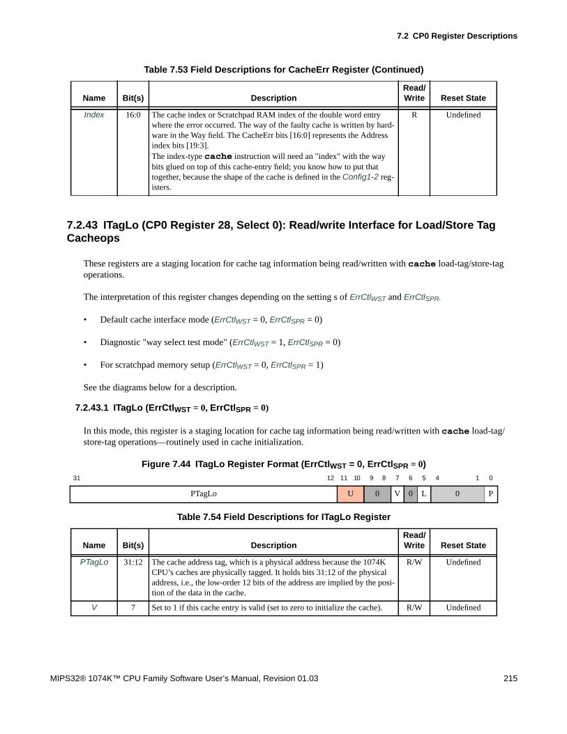
7.2 CP0 Register Descriptions
MIPS32® 1074K™ CPU Family Software User’s Manual, Revision 01.03 215
7.2.43 ITagLo (CP0 Register 28, Select 0): Read/write Interface for Load/Store TagCacheops
These registers are a staging location for cache tag information being read/written with cache load-tag/store-tagoperations.
The interpretation of this register changes depending on the setting s of ErrCtlWST and ErrCtlSPR.
• Default cache interface mode (ErrCtlWST = 0, ErrCtlSPR = 0)
• Diagnostic "way select test mode" (ErrCtlWST = 1, ErrCtlSPR = 0)
• For scratchpad memory setup (ErrCtlWST = 0, ErrCtlSPR = 1)
See the diagrams below for a description.
7.2.43.1 ITagLo (ErrCtlWST = 0, ErrCtlSPR = 0)
In this mode, this register is a staging location for cache tag information being read/written with cache load-tag/store-tag operations—routinely used in cache initialization.
Figure 7.44 ITagLo Register Format (ErrCtlWST = 0, ErrCtlSPR = 0)
Index 16:0 The cache index or Scratchpad RAM index of the double word entrywhere the error occurred. The way of the faulty cache is written by hard-ware in the Way field. The CacheErr bits [16:0] represents the Addressindex bits [19:3].The index-type cache instruction will need an "index" with the waybits glued on top of this cache-entry field; you know how to put thattogether, because the shape of the cache is defined in the Config1-2 reg-isters.
R Undefined
31 12 11 10 9 8 7 6 5 4 1 0
PTagLo U 0 V 0 L 0 P
Table 7.54 Field Descriptions for ITagLo Register
Name Bit(s) DescriptionRead/Write Reset State
PTagLo 31:12 The cache address tag, which is a physical address because the 1074KCPU’s caches are physically tagged. It holds bits 31:12 of the physicaladdress, i.e., the low-order 12 bits of the address are implied by the posi-tion of the data in the cache.
R/W Undefined
V 7 Set to 1 if this cache entry is valid (set to zero to initialize the cache). R/W Undefined
Table 7.53 Field Descriptions for CacheErr Register (Continued)
Name Bit(s) DescriptionRead/Write Reset State
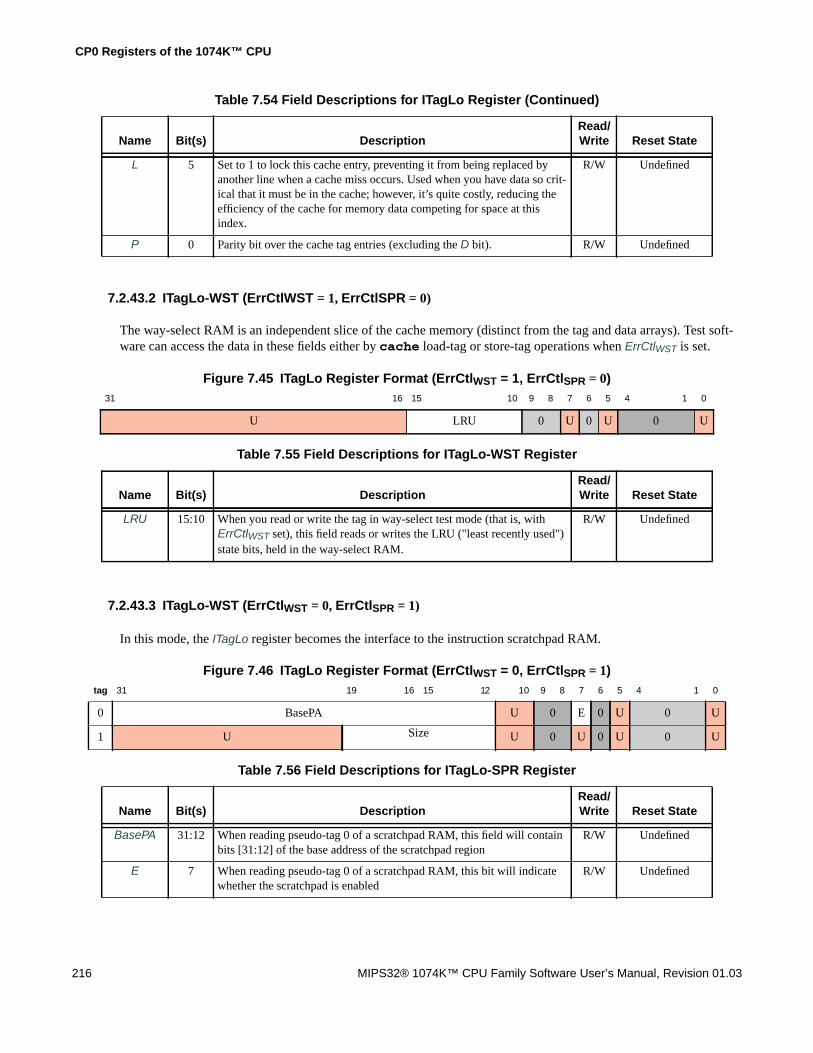
CP0 Registers of the 1074K™ CPU
216 MIPS32® 1074K™ CPU Family Software User’s Manual, Revision 01.03
7.2.43.2 ITagLo-WST (ErrCtlWST = 1, ErrCtlSPR = 0)
The way-select RAM is an independent slice of the cache memory (distinct from the tag and data arrays). Test soft-ware can access the data in these fields either by cache load-tag or store-tag operations when ErrCtlWST is set.
Figure 7.45 ITagLo Register Format (ErrCtlWST = 1, ErrCtlSPR = 0)
7.2.43.3 ITagLo-WST (ErrCtlWST = 0, ErrCtlSPR = 1)
In this mode, the ITagLo register becomes the interface to the instruction scratchpad RAM.
Figure 7.46 ITagLo Register Format (ErrCtlWST = 0, ErrCtlSPR = 1)
L 5 Set to 1 to lock this cache entry, preventing it from being replaced byanother line when a cache miss occurs. Used when you have data so crit-ical that it must be in the cache; however, it’s quite costly, reducing theefficiency of the cache for memory data competing for space at thisindex.
R/W Undefined
P 0 Parity bit over the cache tag entries (excluding the D bit). R/W Undefined
31 16 15 10 9 8 7 6 5 4 1 0
U LRU 0 U 0 U 0 U
Table 7.55 Field Descriptions for ITagLo-WST Register
Name Bit(s) DescriptionRead/Write Reset State
LRU 15:10 When you read or write the tag in way-select test mode (that is, withErrCtlWST set), this field reads or writes the LRU ("least recently used")state bits, held in the way-select RAM.
R/W Undefined
tag 31 19 16 15 12 10 9 8 7 6 5 4 1 0
0 BasePA U 0 E 0 U 0 U
1 U Size U 0 U 0 U 0 U
Table 7.56 Field Descriptions for ITagLo-SPR Register
Name Bit(s) DescriptionRead/Write Reset State
BasePA 31:12 When reading pseudo-tag 0 of a scratchpad RAM, this field will containbits [31:12] of the base address of the scratchpad region
R/W Undefined
E 7 When reading pseudo-tag 0 of a scratchpad RAM, this bit will indicatewhether the scratchpad is enabled
R/W Undefined
Table 7.54 Field Descriptions for ITagLo Register (Continued)
Name Bit(s) DescriptionRead/Write Reset State

7.2 CP0 Register Descriptions
MIPS32® 1074K™ CPU Family Software User’s Manual, Revision 01.03 217
7.2.44 IDataLo (CP0 Register 28, Select 1): Read/write Interface for I-cache SpecialCacheops
Staging registers for special cache instruction which loads or stores data from or to the cache line. Two registers(IDataHi, IDataLo) are needed, because the 1074K CPU loads I-cache data at least 64 bits at a time.
Figure 7.47 IDataLo Register Format
7.2.45 DTagLo (CP0 Register 28, Select 2): Read/Write Interface for Load/Store TagCacheops
These registers are a staging location for cache tag information being read/written with cache load-tag/store-tagoperations. The D-cache has five logical memory arrays associated with this DTagLo register. The tag RAM storestags and other state bits with special attention to the needs of the CPU. The duplicate tag RAM also stores tags andstate, but is optimized for the needs of interventions. Both of these arrays are set-associative (4-way). The Dirty RAMand duplicate Dirty RAM store the dirty bits (indicating modified data) for CPU and intervention uses, and each com-bine their ways together in a single entry per set. The WS RAM also combines the lock and LRU data in a singleentry per set. Accessing these arrays for index cache loads and stores is controlled by using three bits in the ErrCtlregister to create modes that allow the correct access to these arrays.
The interpretation of this register changes depending on the settings of ErrCtlWST, ErrCtlDYT, and ErrCtlSPR.
• Default cache interface mode (ErrCtlWST = 0, ErrCtlDYT = 0, ErrCtlSPR = 0)
• Diagnostic "way select test mode" (ErrCtlWST = 1, ErrCtlDYT = 0, ErrCtlSPR = 0)
• Diagnostic "dirty array test mode" (ErrCtlWST = 0, ErrCtlDYT = 1, ErrCtlSPR = 0)
• For scratchpad memory setup (ErrCtlWST = 0, ErrCtlDYT = 0, ErrCtlSPR = 1)
• Diagnostic “duplicate tag array test mode” (ErrCtlWST = 1, ErrCtlDYT = 0, ErrCtlSPR= 1)
Size 19:12 When reading pseudo-tag 1 of a scratchpad RAM, this field indicates thesize of the scratchpad array. This field is the number of 4KB sections itcontains.
R/W Undefined
31 0
DATA
Table 7.57 IDataLo Register Field Description
Fields
DescriptionRead /Write Reset StateName Bit(s)
DATA 31:0 Low-order data read from the cache data array. R/W Undefined
Table 7.56 Field Descriptions for ITagLo-SPR Register (Continued)
Name Bit(s) DescriptionRead/Write Reset State

CP0 Registers of the 1074K™ CPU
218 MIPS32® 1074K™ CPU Family Software User’s Manual, Revision 01.03
• Diagnostic “duplicate dirty array test mode” (ErrCtlWST = 1, ErrCtlDYT = 1, ErrCtlSPR= 1)
For all modes, the data RAM, tag RAM, WS RAM, and duplicate tag RAM are read. In addition, for duplicate tagarray test mode, the duplicate tag RAM is also read, and for duplicate dirty array test mode, the duplicate Dirty RAMis read. Table 7.58 shows which RAMs are accessed for each mode for Loads and Stores.
7.2.45.1 DTagLo (ErrCtlWST = 0, ErrCtlDYT = 0, ErrCtlSPR = 0)
In this mode, this register is a staging location for cache tag information being read/written with cache load-tag/store-tag operations—routinely used in cache initialization. For stores in this mode, the tag RAM, WS RAM, andduplicate tag RAM are written. Also for stores, the ErrCtlPO bit controls whether the tag RAM is written with P bit orwith generated parity; the other RAMs written in this mode always use generated parity.
Figure 7.48 DTagLo Register Format (ErrCtlWST = 0, ErrCtlDYT = 0, ErrCtlSPR = 0)
Table 7.58 Summary of D-cache RAM accesses for Index Loads and Stores
Mode RAM being accessed
IndexCacheop WST DYT SPR
PrimaryTag RAM WS RAM Data RAM Dirty RAM
DuplicateTag RAM
DuplicateDirty RAM
Tag Store 0 0 0 WR partial WR RD WR
Tag Load 0 0 0 RD RD RD RD
Tag Store 1 0 0 partial WR RD
Tag Load 1 0 0 RD RD RD RD
Data Store 1 0 0 WR
Tag Store 0 1 0 RD WR WR
Tag Load 0 1 0 RD RD RD RD
Tag Store 1 0 1 RD WR
Tag Load 1 0 1 RD RD RD RD RD
Tag Store 1 1 1 RD WR
Tag Load 1 1 1 RD RD RD RD RD
31 12 11 10 8 7 6 5 4 2 1 0
PTag U X 0 V E L 0 P1 P0
Table 7.59 Field Descriptions for DTagLo Register
Name Bit(s) DescriptionRead/Write Reset State
PTag 31:12 The cache address tag — a physical address because the 1074K CPU’scaches are physically tagged. It holds bits 31-12 of the physical address— the low 12 bits of the address are implied by the position of the data inthe cache.Index Load: load from PTag field in primary tag RAMIndex Store: store to PTag field in primary and duplicate tag RAM
R/W Undefined
U 11 This bit always gets the virtual address bit [11] of the tag if the index loadtag cache instruction is executed.
R/W Undefined

7.2 CP0 Register Descriptions
MIPS32® 1074K™ CPU Family Software User’s Manual, Revision 01.03 219
7.2.45.2 DTagLo-WST(ErrCtlWST = 1, ErrCtlDYT = 0, ErrCtlSPR = 0)
The way-select RAM is an independent slice of the cache memory (distinct from the tag and data arrays). Test soft-ware can access either by cache load-tag/store-tag operations when ErrCtlWST is set: then you get the data in thesefields. For stores in this mode, the WS RAM is written. Also for stores, the ErrCtlPO bit controls whether the WSRAM is written with LP bits or with generated parity; the other RAMs written in this mode always use generated par-ity. Also for stores, the LP and L fields only have the appropriate way written in the WS RAM; the onus is on soft-ware to maintain consistency with the value of the L field written into the duplicate tag RAM.
Figure 7.49 DTagLo Register Format (ErrCtlWST = 1, ErrCtlDYT = 0, ErrCtlSPR = 0)
X 10 Unused R/W Undefined
V 7 1 if this cache entry is valid (set zero to initialize the cache).Index Load: load from V field in primary tag RAMIndex Store: store to V field in primary and duplicate tag RAM
R/W Undefined
E 6 1 if this cache entry is exclusive (set zero to initialize the cache).Index Load: load from E field in primary tag RAMIndex Store: store to E field in primary tag RAM
R/W Undefined
L 5 1 to lock this cache entry, preventing it from being replaced by anotherline when there’s a cache miss. Done when you have data so critical thatit must be in the cache: it’s quite costly, reducing the efficiency of thecache for memory data competing for space at this index.Index Load: load from appropriate way of L field in WS RAMIndex Store: store to appropriate way of L and LP field in WS RAM, andif V is set, make selected way MRU in WS RAM; also, store to L field ofduplicate tag RAM.
R/W Undefined
P1 1 Parity bit over the VTAG, G, and ASID bits of cache tag entriesIndex Load: load from PV field in primary tag RAMIndex Store: possible write value for the PV field of the primary tagRAM; write this bit if ErrCtl.PO=1, else generate; parity written to otherRAMs is generated.
R/W Undefined
P0 0 Parity bit over the PTAG, E, and V bits of the cache tag entriesIndex Load: load from PP field in primary tag RAMIndex Store: possible write value for the PP field of the primary tagRAM; write this bit if ErrCtl.PO=1, else generate; parity written to otherRAMs is generated.
R/W Undefined
31 24 23 20 19 16 15 10 9 8 7 6 5 4 2 1 0
U LP L LRU 0 U U U 0 U U
Table 7.59 Field Descriptions for DTagLo Register (Continued)
Name Bit(s) DescriptionRead/Write Reset State

CP0 Registers of the 1074K™ CPU
220 MIPS32® 1074K™ CPU Family Software User’s Manual, Revision 01.03
7.2.45.3 DTagLo-DYT (ErrCtlWST = 0, ErrCtlDYT = 1, ErrCtlSPR = 0)
The dirty RAM is another slice of the cache memory (distinct from the tag and data arrays). Test software can accesseither by cache load-tag/store-tag operations when ErrCtlDYT is set: then you get the data in these fields. For stores,the Dirty RAM is written. For stores, the Dirty RAM and duplicate Dirty RAM are written. Also for stores, theErrCtlPO bit controls whether the Dirty RAM is written with DP bits or with generated parity; the other RAMs writtenin this mode always use generated parity.
Figure 7.50 Field Descriptions for DTagLo-DYT Register
r
Figure 7.51 DTagLo-SPT (ErrCtlWST = 0, ErrCtlDYT = 0, ErrCtlSPR = 1)
Table 7.60 Field Descriptions for DTagLo-WST Register
Name Bit(s) DescriptionRead/Write Reset State
LP 23:20 Parity for Cache-line locking control bits, held in the way select RAM.Each bit of this field is a parity bit for the corresponding bit in the L field.Index Load: load from LP field of WS RAMIndex Store: store to appropriate way of LP field of WS RAM ifErrCtlPO=1,else generate;
R/W Undefined
L 19:16 Cache-line locking control bits, held in the way select RAM.Index Load: load from L field of WS RAMIndex Store: store to appropriate way of L field of WS RAM.
R/W Undefined
LRU 15:10 When you read or write the tag in way select test mode (that is, withErrCtlWST set) this field reads or writes the LRU ("least recently used")state bits, held in the way select RAM.Index Load: load from LRU field of WS RAMIndex Store: store to LRU field of WS RAM
R/W Undefined
31 24 23 20 19 16 15 12 11 10 9 8 7 6 5 4 2 1 0
U DP D U A 0 U U U 0 U U
Table 7.61 Field Descriptions for DTagLo-DYT Register
Name Bit(s) DescriptionRead/Write Reset State
DP 23:20 Parity for Cache line "dirty" bits.Index Load: load from DP field of Dirty RAMIndex Store: store to DP field of Dirty RAM if ErrCtlPO=1, else generate;generate parity for store to duplicate Dirty RAM
R/W Undefined
D 19:16 Cache line "dirty" bits.Index Load: load from D field of Dirty RAMIndex Store: store to D field of Dirty RAM and duplicate Dirty RAM
R/W Undefined
A 11:10 Cache line "alias" bits.Index Load: load from A field of Dirty RAMIndex Store: store 0 and A[10] to A field of Dirty RAM
R/W Undefined

7.2 CP0 Register Descriptions
MIPS32® 1074K™ CPU Family Software User’s Manual, Revision 01.03 221
If your CPU has scratchpad RAM, you will need to initialize and manage it using cache load/store operations whileErrCtlSPR is set. The tag load/store operations are used to read and write control registers: and then you see thesefields.
Figure 7.52 DTagLo Register Format (ErrCtlWST = 0, ErrCtlDYT = 0, ErrCtlSPR = 1)
7.2.45.4 DTagLo-DDTag (ErrCtlWST = 1, ErrCtlDYT = 0, ErrCtlSPR = 1)
The duplicate tag RAM keeps tag state that is checked by interventions due to multiprocessing. In this mode, theduplicate tag RAM can be loaded and stored independently of the (primary) tag RAM. For stores in this mode, onlythe duplicate tag RAM is written.
Figure 7.53 DTagLo Register Format (ErrCtlWST = 1, ErrCtlDYT = 0, ErrCtlSPR = 1)
31 12 11 10 9 8 7 6 5 4 1 0
PTAG U 0 E 0 U 0 U
Table 7.62 Field Descriptions for DTagLo-SPT Register
Name Bit(s) DescriptionRead/Write Reset State
PTAG 31:12 Scratchpad control. Sets base address. R/W Undefined
E 7 Scratchpad control enable. R/W Undefined
31 12 11 10 8 7 6 5 4 1 0
PTag U X 0 V U L 0 P1 P0
Table 7.63 Field Descriptions for DTagLo-DDTag Register
Name Bit(s) DescriptionRead/Write Reset State
PTag 31:12 The cache address tag — a physical address because the 1074K CPU’scaches are physically tagged. It holds bits 31-12 of the physical address— the low 12 bits of the address are implied by the position of the data inthe cache.Index Load: load from PTag filed in duplicate tag RAMIndex Store: store to PTag field in duplicate tag RAM
R/W Undefined
U 11 This bit always gets the virtual address bit [11] of the tag if the index loadtag cache instruction is executed.Index Load: load from U field in duplicate tag RAMIndex Store: store to U field in duplicate tag RAM
R/W Undefined
X 10 Unused R/W Undefined

CP0 Registers of the 1074K™ CPU
222 MIPS32® 1074K™ CPU Family Software User’s Manual, Revision 01.03
7.2.45.5 DTagLo-DDYT (ErrCtlWST = 1, ErrCtlDYT = 1, ErrCtlSPR= 1)
The duplicate Dirty RAM keeps dirty state that is checked by interventions due to multiprocessing. In this mode, theduplicate Dirty RAM can be loaded and stored independently of the (primary) Dirty RAM. For stores in this mode,only the duplicate Dirty RAM is written.
Figure 7.54 Field Descriptions for DTagLo-DDYT Register
V, L 7, 5 For duplicate tag ram, these 2 bits encode the state of the cache line (setzero to initialize the cache).Index Load: load from V & L field in duplicate tag RAMIndex Store: store to V & L field in duplicate tag RAM
R/W Undefined
P1 0 Parity bit over the L bit of the cache tag entriesIndex Load: load from P field in duplicate tag RAMIndex Store: possible write value for the P field of the duplicate tagRAM; write this bit if ErrCtl.PO=1, else generate
R/W Undefined
P0 0 Parity bit over the all bits except the L bit of the cache tag entriesIndex Load: load from P field in duplicate tag RAMIndex Store: possible write value for the P field of the duplicate tagRAM; write this bit if ErrCtl.PO=1, else generate
R/W Undefined
31 24 23 20 19 16 15 12 11 10 9 8 7 6 5 4 1 0
U DP D U A 0 U U U 0 U U
Table 7.64 Field Descriptions for DTagLo-DDYT Register
Name Bit(s) DescriptionRead/Write Reset State
DP 23:20 Parity for Cache line "dirty" bits.Index Load: load from DP field of duplicate Dirty RAMIndex Store: store to DP field of duplicate Dirty RAM if ErrCtlPO=1, elsegenerate
R/W Undefined
D 19:16 Cache line "dirty" bits.Index Load: load from D field of duplicate Dirty RAMIndex Store: store to D field of duplicate Dirty RAM
R/W Undefined
A 11:10 Cache line "alias" bits.Index Load: load zeroesIndex Store: none
R/W Undefined
Table 7.63 Field Descriptions for DTagLo-DDTag Register (Continued)
Name Bit(s) DescriptionRead/Write Reset State
VL encoding Meaning
00 Invalid
01 Shared
10 Exclusive (Modified if Duplicate Dirty is set)
11 Lock

7.2 CP0 Register Descriptions
MIPS32® 1074K™ CPU Family Software User’s Manual, Revision 01.03 223
7.2.46 DDataLo (CP0 Register 28, Select 3): Low-order Data Read/Write Interface forD-cache
On 1074K family cores, test software can read or write cache data using a cache index load tag/index store datainstruction. Which word of the cache line is transferred depends on the low address fed to the cache instruction.
Figure 7.55 DDataLo Register Format
7.2.47 L23TagLo (CP0 Register 28, Select 4): L2 and L3 Cacheop Tag Use
This register in the 1074K CPU is implemented to support access to external L2 cache tags via cache instructions.The definition of the fields of this 32 bit register are defined by the SoC designer. Refer to the section on L2 Transac-tions in the document ““MIPS32® 1074K™ CPU Family Integrator’s Guide, MD00499” for further information onusing this register.
Figure 7.56 L23TagLo Register Format
7.2.48 L23DataLo (CP0 Register 28, Select 5): Low-order Data Read/Write Interface forL2 or L3 cache
On 1074K family cores, test software can read or write cache data using a cache index load/store data instruction.Which word of the cache line is transferred depends on the low address fed to the cache instruction.
Figure 7.57 L23DataLo Register Format
31 0
DATA
Table 7.65 DDataLo Register Field Description
Fields
DescriptionRead /Write Reset StateName Bit(s)
DATA 31:0 Low-order data read from the cache data array. R/W Undefined
31 0
DATA
31 0
DATA
Table 7.66 L23DataLo Register Field Description
Fields
DescriptionRead /Write Reset StateName Bit(s)
DATA 31:0 Low-order data read from the cache data array. R/W Undefined
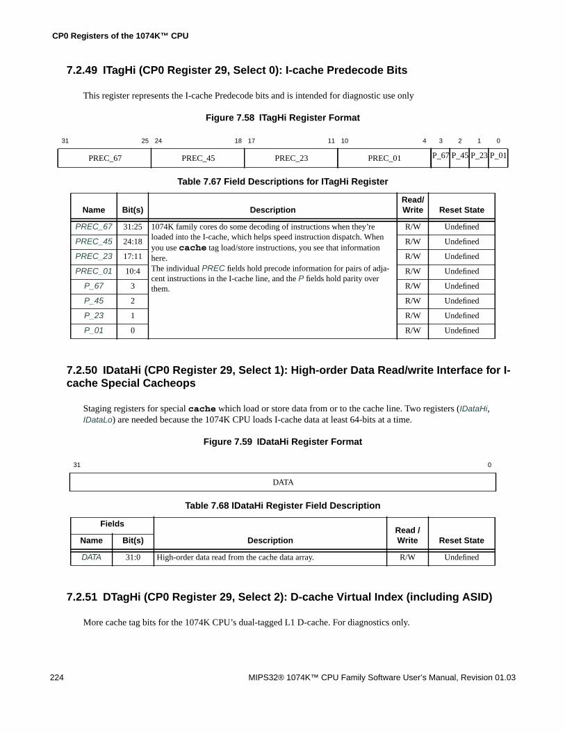
CP0 Registers of the 1074K™ CPU
224 MIPS32® 1074K™ CPU Family Software User’s Manual, Revision 01.03
7.2.49 ITagHi (CP0 Register 29, Select 0): I-cache Predecode Bits
This register represents the I-cache Predecode bits and is intended for diagnostic use only
Figure 7.58 ITagHi Register Format
7.2.50 IDataHi (CP0 Register 29, Select 1): High-order Data Read/write Interface for I-cache Special Cacheops
Staging registers for special cache which load or store data from or to the cache line. Two registers (IDataHi,IDataLo) are needed because the 1074K CPU loads I-cache data at least 64-bits at a time.
Figure 7.59 IDataHi Register Format
7.2.51 DTagHi (CP0 Register 29, Select 2): D-cache Virtual Index (including ASID)
More cache tag bits for the 1074K CPU’s dual-tagged L1 D-cache. For diagnostics only.
31 25 24 18 17 11 10 4 3 2 1 0
PREC_67 PREC_45 PREC_23 PREC_01 P_67 P_45 P_23 P_01
Table 7.67 Field Descriptions for ITagHi Register
Name Bit(s) DescriptionRead/Write Reset State
PREC_67 31:25 1074K family cores do some decoding of instructions when they’reloaded into the I-cache, which helps speed instruction dispatch. Whenyou use cache tag load/store instructions, you see that informationhere.The individual PREC fields hold precode information for pairs of adja-cent instructions in the I-cache line, and the P fields hold parity overthem.
R/W Undefined
PREC_45 24:18 R/W Undefined
PREC_23 17:11 R/W Undefined
PREC_01 10:4 R/W Undefined
P_67 3 R/W Undefined
P_45 2 R/W Undefined
P_23 1 R/W Undefined
P_01 0 R/W Undefined
31 0
DATA
Table 7.68 IDataHi Register Field Description
Fields
DescriptionRead /Write Reset StateName Bit(s)
DATA 31:0 High-order data read from the cache data array. R/W Undefined

7.2 CP0 Register Descriptions
MIPS32® 1074K™ CPU Family Software User’s Manual, Revision 01.03 225
Figure 7.60 DTagHi Register Format
7.2.52 L23DataHi (CP0 Register 29, Select 5): High-order Data Read/Write Interface forL2 or L3 cache
On 1074K family cores, test software can read or write cache data using a cache index load/store data instruction.Which word of the cache line is transferred depends on the low address fed to the cache instruction.
Figure 7.61 L23DataHi Register Format
7.2.53 ErrorEPC (CP0 Register 30, Select 0): Restart Location from Reset or CacheError Exception
This full 32-bit register is filled with the restart address on a cache error exception or any kind of CPU reset — in fact,any exception which sets StatusERL and leaves the CPU in "error mode".
Figure 7.62 ErrorEPC Register Format
31 12 11 10 9 8 7 0
VTAG U 0 G ASID
Table 7.69 Field Descriptions for DTagHi Register
Name Bit(s) DescriptionRead/Write Reset State
VTAG 31:12 1074K family cores have a dual-tagged D-cache, combining a virtual tagfor fast lookup with a physical tag to avoid aliases.Bit[11] always gets virtual address[11] of the tag when index load tagcache instruction is executed.These fields store the information required to match a virtual address: thevirtual address itself, the ASID (tracking the "address space identifier"maintained in EntryHiASID) and a global ("G") bit which can be set tomake it not necessary to match the ASID.
R/W Undefined
U 11 R/W Undefined
G 8 R/W Undefined
ASID 7:0 R/W Undefined
31 0
DATA
Table 7.70 L23DataHi Register Field Description
Fields
DescriptionRead /Write Reset StateName Bit(s)
DATA 31:0 High-order data read from the cache data array. R/W Undefined
31 0
ErrorEPC

CP0 Registers of the 1074K™ CPU
226 MIPS32® 1074K™ CPU Family Software User’s Manual, Revision 01.03
7.2.54 DESAVE (CP0 Register 31, Select 0): Scratch Read/Write Register for EJTAGDebug Exception Handler
Software-only register, with no hardware effect. Provided because the debug exception handler can’t use the k0-1 GPregisters, used by ordinary exception handlers to bootstrap themselves: but a debug handler can save a GPR intoDESAVE, and then use that GPR register in code which saves everything else.
Figure 7.63 DeSave Register Format
Table 7.71 ErrorEPC Register Field Description
Fields
DescriptionRead /Write Reset StateName Bit(s)
ErrorEPC 31:0 Error Exception Program Counter. R/W Undefined
31 0
DESAVE
Table 7.72 DeSave Register Field Description
Fields
DescriptionRead /Write Reset StateName Bit(s)
DESAVE 31:0 Debug exception save contents. SO Undefined

Chapter 8
MIPS32® 1074K™ CPU Family Software User’s Manual, Revision 01.03 227
Hardware and Software Initialization of the 1074K™ CPU
A 1074K CPU contains only a minimal amount of hardware initialization and relies on software to fully initialize thedevice.
This chapter contains the following sections:
• Section 8.1 “Hardware-Initialized Processor State”
• Section 8.2 “Software-Initialized Processor State”
8.1 Hardware-Initialized Processor State
A 1074KCPU, like most other MIPS processors, is not fully initialized by hardware reset. Only a minimal subset ofthe processor state is cleared. This is enough to bring the CPU up while running in unmapped and uncached codespace. All other processor state can then be initialized by software. Unlike previous MIPS processors, there is no dis-tinction between cold and warm resets (or hard and soft resets). SI_Reset is used for both power-up reset and softreset.
8.1.1 Coprocessor 0 State
Much of the hardware initialization occurs in Coprocessor 0:
• Random - cleared to maximum value on Reset (TLB/MMU only)
• Wired - cleared to 0 on Reset (TLB/MMU only)
• StatusBEV - set to 1 on Reset
• StatusTS - cleared to 0 on Reset
• StatusNMI - cleared to 0 on Reset
• StatusERL - set to 1 on Reset
• StatusRP - cleared to 0 on Reset
• CDMMBaseEN - cleared to 0 on Reset
• WatchLoI,R,W - cleared to 0 on Reset
• Config fields related to static inputs - set to input value by Reset
• ConfigK0 - set to 010 (uncached) on Reset

Hardware and Software Initialization of the 1074K™ CPU
228 MIPS32® 1074K™ CPU Family Software User’s Manual, Revision 01.03
• ConfigKU - set to 010 (uncached) on Reset (FMT/MMU only)
• ConfigK23 - set to 010 (uncached) on Reset (FMT/MMU only)
• DebugDM - cleared to 0 on Reset (unless EJTAGBOOT option is used to boot into Debug Mode, as described inChapter 11, “EJTAG Debug Support in the 1074K™ CPU”.
• DebugLSNM - cleared to 0 on Reset
• DebugIBusEP - cleared to 0 on Reset
• DebugDBusEP - cleared to 0 on Reset
• DebugIEXI - cleared to 0 on Reset
• DebugSSt - cleared to 0 on Reset
8.1.2 TLB Initialization
Each TLB entry has a “hidden” state bit, which is set by Reset and is cleared when the TLB entry is written. This bitdisables matches and prevents “TLB Shutdown” conditions from being generated by the power-up values in the TLBarray (when two or more TLB entries match a single address). This bit is not visible to software.
8.1.3 Bus State Machines
All pending bus transactions are aborted and the state machines in the bus interface unit are reset when a Reset excep-tion is taken.
8.1.4 Static Configuration Inputs
All static configuration inputs (for example, those defining the bus mode and cache size) should only be changed dur-ing Reset.
8.1.5 Fetch Address
Upon Reset, unless the EJTAGBOOT option is used, the fetch is directed to VA 0xBFC00000 (PA 0x1FC00000).This address is in kseg1, which is unmapped and uncached, so that the TLB and caches do not require hardware ini-tialization.
8.2 Software-Initialized Processor State
Software is required to initialize parts of the device, as described below.
8.2.1 Register File
The register file powers up in an unknown state with the exception of r0, which is always 0. Initializing the rest of theregister file is not required for proper operation. Good code will generally not read a register before writing to it, butthe boot code can initialize the register file for added safety.

8.2 Software-Initialized Processor State
MIPS32® 1074K™ CPU Family Software User’s Manual, Revision 01.03 229
8.2.2 TLB
Because of the hidden bit indicating initialization, the CPU does not initialize the TLB upon Reset. This is an imple-mentation-specific feature of the 1074K CPU and cannot be relied upon if writing generic code for MIPS32/64 pro-cessors.
8.2.3 Caches
The cache tag and data arrays power up to an unknown state and are not affected by reset. Every tag in the cachearrays should be initialized to an invalid state using the CACHE instruction (typically the Index Invalidate function).This can be a long process, especially because the instruction cache initialization must run in an uncached addressregion.
8.2.4 Coprocessor 0 State
Miscellaneous COP0 states need to be initialized before exiting the boot code. There are various exceptions which areblocked by ERL=1 or EXL=1, and which are not cleared by Reset. These can be cleared to avoid taking spuriousexceptions when leaving the boot code.
• Cause: WP (Watch Pending), and SW0 and SW1 (Software Interrupts) should be cleared.
• Config: K0 should be set to the desired Cache Coherency Algorithm (CCA) prior to accessing kseg0.
• Config: (FM MMU only) KU and K23 should be set to the desired CCA for useg/kugeg and kseg2/3 respectivelyprior to accessing those regions.
• Count: Should be set to a known value if timer tnterrupts are used.
• Compare: Should be set to a known value if timer tnterrupts are used. Note that the write to Compare will alsoclear any pending timer interrupts, so Count should be set before Compare to avoid any unexpected interrupts.
• Status: Desired state of the device should be set.
• Other COP0 state: Other registers should be written before they are read. Some registers are not explicitly write-able, and are only updated as a by-product of instruction execution or a taken exception. Uninitialized bits shouldbe masked off after reading these registers.
8.2.5 Multi-CPU Initialization
When the 1074K Coherent Processing System is reset, only one CPU will initially be enabled. Additional steps arerequired to start the other CPUs in the cluster and to enable cache coherence between them. Refer to the MIPS32®1074K™ Coherent Processing System User's Manual (MD00748) [5] for more details.

Hardware and Software Initialization of the 1074K™ CPU
230 MIPS32® 1074K™ CPU Family Software User’s Manual, Revision 01.03

Chapter 9
MIPS32® 1074K™ CPU Family Software User’s Manual, Revision 01.03 231
Caches of the 1074K™ CPU
This chapter describes the caches present in a 1074K CPU. It contains the following sections:
• Section 9.1 “Cache Configurations”
• Section 9.2 “Instruction Cache”
• Section 9.3 “Data Cache”
• Section 9.4 “Write Back Buffer”
• Section 9.5 “Cache Protocols”
• Section 9.6 “CACHE Instruction”
• Section 9.7 “Software Cache Testing”
• Section 9.8 “Memory Coherence Issues”
9.1 Cache Configurations
A 1074K CPU has separate instruction and data caches, which allows instruction and data references to proceedsimultaneously. Each of the caches is 4-way set associative. The instruction cache can be configured at build time tobe 0, 16, 32, or 64KB, and the data cache can be configured at build time to be 16, 32, or 64KB. Both caches use a32B line size and support locking on a per line basis. Parity protection of the cache arrays is an optional feature.
9.2 Instruction Cache
Table 9.1 shows the key characteristics of the instruction cache. Figure 9.1 shows the format of an entry in the threearrays comprising the instruction cache: data, tag, and way-select.
Table 9.1 Instruction Cache Attributes
Attribute With Parity Without Parity
Size 0, 16, 32, 64KB
Line Size 32B
Number of Cache Sets 128, 256, 512
Associativity 4 way
Replacement LRU
Cache Locking per line
Data Array

Caches of the 1074K™ CPU
232 MIPS32® 1074K™ CPU Family Software User’s Manual, Revision 01.03
Figure 9.1 Instruction Cache Organization
9.2.1 Virtual Aliasing
The instruction cache on the 1074K CPU is virtually indexed and physically tagged. The lower bits of the virtualaddress are used to access the cache arrays and the physical address is used in the tags. Because the way size can belarger than the minimum TLB page size, there is a potential for virtual aliasing. This means that one physical addresscan exist in multiple indices within the cache, if it is accessed with different virtual addresses. Virtual aliasing comesinto effect only for cache sizes that are larger than 16KB. The 16KB cache size does not suffer from virtual aliasing,because the way size equals the minimum page size.
This reduces the cache efficiency somewhat, but is generally not a problem unless the instruction stream is being writ-ten to. When instructions are written, software must ensure that the store data is written out to memory and the olddata is invalidated in the instruction cache (via the CACHE or SYNCI instruction). Because one physical address canexist in multiple locations, the cache should be invalidated using all of the virtual addresses used to access that physi-cal address. The hardware implementation takes care of this automatically when Config7.IVA bit is cleared. In theabsence of the hardware feature, alternatively, all of the relevant cache indices or the entire cache can be invalidated.
9.2.2 Precode bits
In order for the fetch unit to quickly detect branches and jumps when executing code, the instruction cache array con-tains some additional precode bits. These bits indicate the type and location of branch or jump instructions within a64b fetch bundle. These precode bits are not used when executing MIPS16e code.
Read Unit 144b x 4 128b x 4
Write Unit 144b 128b
Tag Array
Read Unit 55b x 4 50b x 4
Write Unit 55b 50b
Way-Select Array
Read Unit 6b
Write Unit 1-6b
Table 9.1 Instruction Cache Attributes (Continued)
Attribute With Parity Without Parity
Tag (per way):
Data (per way)1:
Way-Select:
5 1 1 20 7 7 7 7
Parity Valid Lock PA[31:12] Precode_67 Precode_45 Precode_23 Precode_01
16 64 64 16 64 64
Parity dword3 dword2 Parity dword1 dword0
6
LRU
1. Parity bits in data array will be interleaved with precode and data bytes.
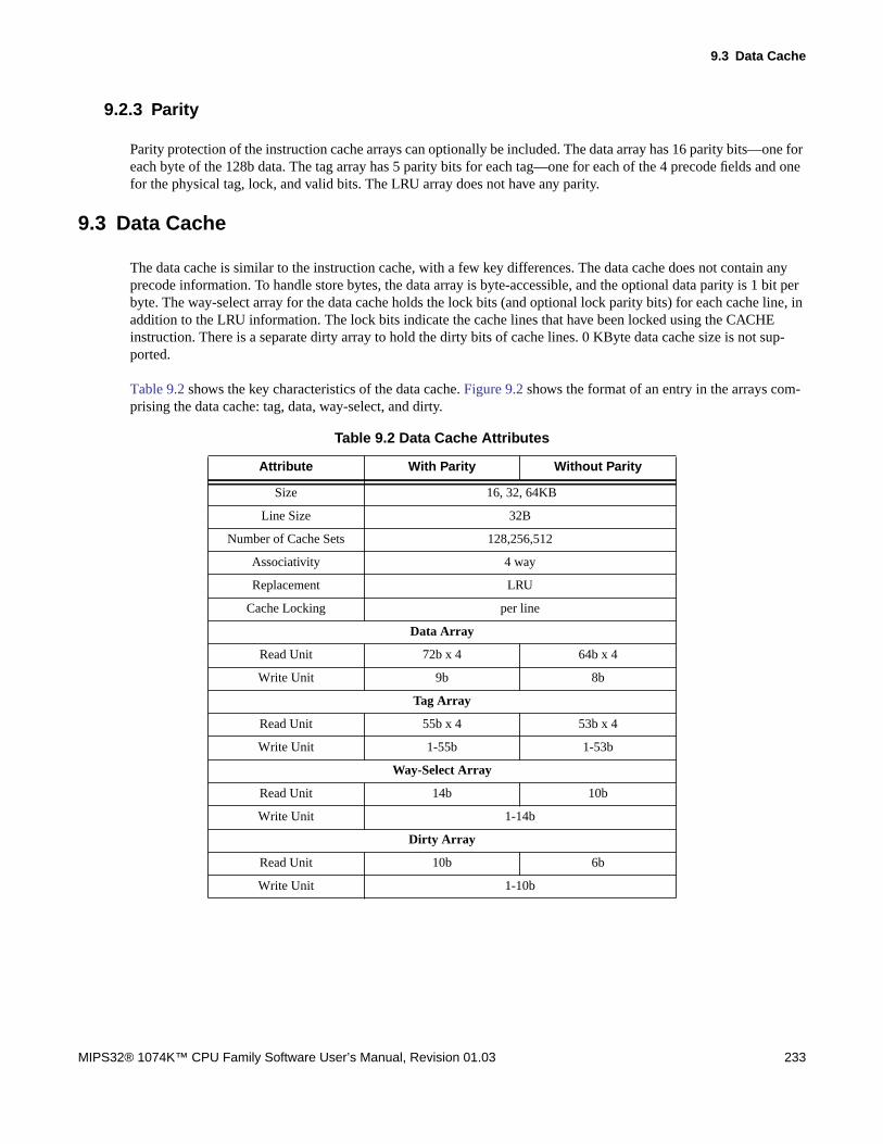
9.3 Data Cache
MIPS32® 1074K™ CPU Family Software User’s Manual, Revision 01.03 233
9.2.3 Parity
Parity protection of the instruction cache arrays can optionally be included. The data array has 16 parity bits—one foreach byte of the 128b data. The tag array has 5 parity bits for each tag—one for each of the 4 precode fields and onefor the physical tag, lock, and valid bits. The LRU array does not have any parity.
9.3 Data Cache
The data cache is similar to the instruction cache, with a few key differences. The data cache does not contain anyprecode information. To handle store bytes, the data array is byte-accessible, and the optional data parity is 1 bit perbyte. The way-select array for the data cache holds the lock bits (and optional lock parity bits) for each cache line, inaddition to the LRU information. The lock bits indicate the cache lines that have been locked using the CACHEinstruction. There is a separate dirty array to hold the dirty bits of cache lines. 0 KByte data cache size is not sup-ported.
Table 9.2 shows the key characteristics of the data cache. Figure 9.2 shows the format of an entry in the arrays com-prising the data cache: tag, data, way-select, and dirty.
Table 9.2 Data Cache Attributes
Attribute With Parity Without Parity
Size 16, 32, 64KB
Line Size 32B
Number of Cache Sets 128,256,512
Associativity 4 way
Replacement LRU
Cache Locking per line
Data Array
Read Unit 72b x 4 64b x 4
Write Unit 9b 8b
Tag Array
Read Unit 55b x 4 53b x 4
Write Unit 1-55b 1-53b
Way-Select Array
Read Unit 14b 10b
Write Unit 1-14b
Dirty Array
Read Unit 10b 6b
Write Unit 1-10b

Caches of the 1074K™ CPU
234 MIPS32® 1074K™ CPU Family Software User’s Manual, Revision 01.03
Figure 9.2 Data Cache Organization
9.3.1 Virtual Aliasing
The 1074K must be configured with hardware anti-aliasing support for the data cache when the cache size (32KB or64KB) and MMU type (TLB) make it subject to aliases. With this hardware, the data cache is effectively physicallyindexed and tagged.
9.3.2 Parity
Parity protection of the data cache arrays can optionally be included. The data array requires a parity bit for each byte,corresponding to the minimum write quantum for a store. The tag array has a single parity bit for each tag. The way-select array has separate parity bits to cover each lock bit, but the LRU bits are not covered by parity. The dirty arrayalso has a parity bit for each dirty bit.
9.4 Write Back Buffer
The BIU includes a Write Back Buffer (WBB) that holds writes going to memory. This includes evictions from thedata cache, as well as uncached stores, and uncached accelerated stores. The WBB consists of 8 entries, each ofwhich is capable of holding 32B of data. The WBB also holds L2 CACHE instructions that are to be sent out on thebus.
The WBB will attempt to gather uncached accelerated (UCA) stores to allow full line burst writes. UCA behavior isdescribed in Section 9.4.1 “Uncached Accelerated Stores”.
WBB entries are ‘flushed’ under a variety of conditions. When a buffer is flushed, the write command is queued inthe BIU and the WBB entry will not accept any more activity until the data has been written to the bus and the bufferis freed up. UCA flush conditions are described in the next section. Flush conditions for other types are shown here:
• Uncached (non-accelerated) stores flush immediately
• L2 CACHE instruction commands are also flushed immediately
Data (per way):
Way-Select:
1 8 9x30 1 8
Parity Data31 ... Parity Data0
4 4 6
Lock Parity Lock LRU
2 4 4
Reserved Dirty Parity DirtyDirty
Tag (per way): 1 1 1 21 1 8 21 1
Parity Parity State PA[31:11] Global ASID VA[31:11] Valid

9.4 Write Back Buffer
MIPS32® 1074K™ CPU Family Software User’s Manual, Revision 01.03 235
• Entries for D$ evictions are flushed when all 4 dwords (32B) of data have been gathered
When coherence is enabled, the CPU is the ‘owner’ of a cache line until the self-intervention for the writebackrequest has been seen. The WBB entry cannot be deallocated until that point so that the CPU can respond with thedata if another CPU requests it. The WBB is also used for staging data responses to interventions. To avoid deadlock,one WBB entry must be reserved for this purpose.
9.4.1 Uncached Accelerated Stores
Uncached Accelerated gathering is supported for word and doubleword stores only.
Gathering of uncached accelerated stores will start on cache-line aligned addresses, i.e. 32 byte aligned addresses.Uncached accelerated word or doubleword stores that do not to meet the conditions required to start gathering will betreated like regular uncached stores.
When an uncached accelerated store meets the requirements needed to start gathering, a gather buffer is reserved forthis store. All subsequent uncached accelerated word or doubleword stores to the same cache line will write sequen-tially into this buffer, regardless of the word address associated with these stores. The uncached accelerated buffer istagged with the address of the first store.
An uncached accelerated buffer is written to memory (flushed) if:
1. The last word in the entry being gathered is written (implicit flush).
2. A PREF Nudge which match the address associated with the gather buffer (explicit flush).
3. A SYNC instruction is executed (Explicit flush).
4. Bits <31:5> of the address of a Load instruction match the address associated with the gather buffer (implicitflush).
5. Uncached Accelerated store to a different 32B line (implicit flush).
6. An exception occurs (implicit flush).
When an uncached accelerated buffer is flushed, the address sent out on the system interface is the address associatedwith the gather buffer.
Caveats:
• Any uncached stores and any uncached loads to unrelated addresses that occur between uncached acceleratedstores that are part of a gather sequence will go out-of-order. They will not enforce ordering.
• The only constraint imposed on the gathering is that doubleword stores are only allowed to write to doubleword-aligned locations in the buffer. For example, if uncached accelerated gathering starts with a Store Word (SW), itmay not be followed by a Store Double (SDC1).
• Uncached accelerated stores of the following types are not intended to be used by software and may generateunpredictable results:
1. Halfword Stores
2. Unaligned Stores

Caches of the 1074K™ CPU
236 MIPS32® 1074K™ CPU Family Software User’s Manual, Revision 01.03
3. Store conditionals
• In order for software to execute correctly on implementations without uncached accelerated stores, softwareshould always generate accesses starting on a cache-line aligned address, proceed to generate correctly incre-mented sequential addresses, and observe the restrictions for uncached accelerated stores.
9.5 Cache Protocols
This section describes cache organization, attributes, and cache-line replacement for the instruction and data caches.This section also discusses issues relating to virtual aliasing.
9.5.1 Cache Organization
The instruction and data caches each consist of three arrays: tag, data, and way-select. In addition, the data cache hasa dirty array. The caches are virtually indexed, since a virtual address is used to select the appropriate line within eachof the three arrays. The caches are physically tagged, as the tag array contains a physical, not virtual, address.
The tag and data arrays hold 4 ways of information per set, corresponding to the 4-way set associativity of the cache.The way-select array holds information to choose the way to be filled, as well as dirty bits in the case of the datacache.
Figure 9.1 (instruction cache) and Figure 9.2 (data cache) show the format of each line in the tag, data, and way-selectarrays.
A tag entry consists of the upper bits of the physical address (bits [31:12] for instruction cache, bits[31:11] for datacache), one valid bit for the line, and a lock bit. A data entry contains the four, 64-bit doublewords in the line, for atotal of 32 bytes. All four words in the line are present or not in the data array together, hence the single valid bitstored with the tag. Once a valid line is resident in the cache, byte, halfword, triple-byte or full word stores can updateall or a portion of the words in that line. The tag and data entries are repeated for each of the 4 lines in the set.
A way-select entry holds bits choosing the way to be replaced according to a Least Recently Used (LRU) algorithm.The LRU information applies to all the ways and there is one way-select entry for all the ways in the set. The arraywith way-select entries for the data cache also holds dirty bits for the lines. One dirty bit is required per line, as shownin Figure 9.2. The instruction cache only supports reads, hence only LRU entries are stored in the instruction way-select array.
9.5.2 Cacheability Attributes
A 1074K CPU supports the following cacheability attributes:
• Uncached: Addresses in a memory area indicated as uncached are not read from the cache. Stores to suchaddresses are written directly to main memory, without changing cache contents.
• Non-coherent Writeback With Write Allocation: Loads and instruction fetches first search the cache, readingmain memory only if the desired data does not reside in the cache. On data store operations, the cache is firstsearched to see if the target address is in the cache. If it is, the cache contents are updated, but main memory isnot written. If the cache lookup misses on a store, main memory is read to bring the line into the cache and mergeit with the new store data. Hence, the allocation policy on a cache miss is read- or write-allocate. Data stores willupdate the appropriate dirty bit in the way-select array to indicate that the line contains modified data. When aline with dirty data is displaced from the cache, it is written back to memory.

9.5 Cache Protocols
MIPS32® 1074K™ CPU Family Software User’s Manual, Revision 01.03 237
• Uncached Accelerated: Uncached stores are gathered together for more efficient bus utilization. See Section9.4.1 “Uncached Accelerated Stores” for more details
• Coherent Write-back With Write Allocation, Exclusive on Write: Use coherent data. Load misses will bring thedata into the cache in a shared state. Multiple caches can contain data in the shared state. Stores will bring datainto the cache in an exclusive state - no other caches can contain that same line. If a store hits on a shared line inthe cache, the line will be invalidated and brought back into the cache in an exclusive state.
• Coherent Write-back With Write Allocation, Exclusive: Similar to the above, but load misses will bring data intothe cache in an exclusive state rather than shared. This can be used if data is not shared and will eventually bewritten. This can reduce bus traffic, because the line does not have to be refetched in an exclusive state when astore is done.
Some segments of memory employ a fixed caching policy; for example, kseg1 is always uncacheable. Other segmentsof memory allow the caching policy to be selected by software. Generally, the cache policy for these programmableregions is defined by a cacheability attribute field associated with that region of memory. See Chapter 5, “MemoryManagement of the 1074K™ CPU” for further details.
9.5.3 Replacement Policy
The replacement policy refers to how a way is chosen to hold an incoming cache line on a miss which will result in acache fill. The replacement policy is least-recently used (LRU), but excluding any locked ways. The LRU bit(s) in theway-select array encode the order in which ways on that line have been accessed.
On a cache miss, the lock and LRU bits for the tag and way-select entries of the selected line may be used to deter-mine the way which will be chosen.
The LRU field in the way select array is updated as follows:
• On a cache hit, the associated way is updated to be the most recently used. The order of the other ways relative toeach another is unchanged.
• On a cache refill, the filled way is updated to be the most recently used.
• On CACHE instructions, the update of the LRU bits depends on the type of operation to be performed:
• Index (Writeback) Invalidate: Least-recently used.
• Index Load Tag: No update.
• Index Store Tag, WST=0: Most-recently used if valid bit is set in TagLo CP0 register. Least-recently used ifvalid bit is cleared in TagLo CP0 register.
• Index Store Tag, WST=1: Update the field with the contents of the TagLo CP0 register (refer to Table 7.60for the valid values of this field).
• Index Store Data: No update.
• Hit Invalidate: Least-recently used if a hit is generated, otherwise unchanged.
• Fill: Most-recently used.
• Hit (Writeback) Invalidate: Least-recently used if a hit is generated, otherwise unchanged.
Caches of the 1074K™ CPU
238 MIPS32® 1074K™ CPU Family Software User’s Manual, Revision 01.03
• Hit Writeback: No update.
• Fetch and Lock: For instruction cache, no update. For data cache, most-recently used.
If all ways are valid, then any locked ways will be excluded from consideration for replacement. For the unlockedways, the LRU bits are used to identify the way which has been used least-recently, and that way is selected forreplacement.
If the way selected for replacement has its dirty bit asserted in the way-select array, then that 32-byte line will be writ-ten back to memory before the new fill can occur.
9.5.4 Line Locking
The 1074K CPU does not support the locking of all 4 ways of either cache at a particular index. If all 4 ways of thecache at a given index are locked by either Fetch and Lock or Index Store Tag CACHE instructions, subsequent cachemisses at that cache index will displace one of the locked lines.
Locking lines in the caches is somewhat counter to the idea of coherence. If a line is locked into a particular cache, itis expected that any processes utilizing that data will be locked to that processor and coherence is not needed. Basedon this usage model, locking coherent lines into the cache is not recommended. If it is done, the CPUs use the follow-ing rules:
• SYNCI instructions are user-mode instructions. Since locking is a kernel mode feature (requires the CACHEinstruction), SYNCI is not allowed to unlock cache lines. This applies to both local and globalized SYNCIinstructions.
• Locking overrides coherence. Intervention requests from other CPUs and I/O devices that match on a locked lineare treated as misses.
• Self-intervention requests for globalized CACHE instructions are allowed to affect a locked line. This is doneprimarily for handling lock and unlock requests for kseg0 addresses when kseg0 is being treated coherently.
• The CPU does not support the locking of all 4 ways of either cache at a particular index. If all 4 ways of the cacheat a given index are locked, subsequent cache misses at that cache index will displace one of the locked lines.
9.6 CACHE Instruction
Both caches support the CACHE instructions, which allow users to manipulate the contents of the Data and Tagarrays, including the locking of individual cache lines. These instructions are described in detail in Chapter 13,“1074K™ CPU Instructions”.
The CACHE Index Load Tag and Index Store Tag instructions can be used to read and write the Way Select (WS)RAM by setting the WST bit in the ErrCtl register. (The ErrCtl register is described in Section 7.2.41 “ErrCtl (CP0Register 26, Select 0): Software Parity Control and Test Modes for Cache RAM Arrays”.) Similarly, the SPR bit inthe ErrCtl register will cause Index Load Tag and Index Store Tag instructions to read the pseudo-tags associated withthe scratchpad RAM array. Note that when the WST and SPR bits are zero, the CACHE index instructions access thecache Tag array.

9.7 Software Cache Testing
MIPS32® 1074K™ CPU Family Software User’s Manual, Revision 01.03 239
Not all values of the WS field are valid for defining the order in which the ways are selected. This is only an issue,however, if the WS RAM is written after the initialization (invalidation) of the Tag array. Valid WS field encodingsfor way selection order is shown in Table 9.3.
9.7 Software Cache Testing
Typically, the cache RAM arrays will be tested using BIST. It is, however, possible for software running on the pro-cessor to test all of the arrays. Of course, testing of the I-cache arrays should be done from an uncacheable space withinterrupts disabled in order to maintain the cache contents. There are multiple methods for testing these arrays in soft-ware, some of which are described in the following subsections.
9.7.1 I-cache and Primary D-cache Tag Arrays
These arrays can be tested via the Index Load Tag and Index Store Tag varieties of the CACHE instruction. IndexStore Tag will write the contents of the ITagLo and ITagHi registers into the selected tag entry. Index Load Tag willread the selected tag entry into the ITagLo and ITagHi registers.
If parity is implemented, the parity bits can be tested as normal bits by setting the PO (parity override) bit in the ErrCtlregister. This will override the parity calculation and use the parity bits in ITagLo and ItagHi as the parity values.
9.7.2 Duplicate D-cache Tag Array
This array can be tested via the Index Load Tag and Index Store Tag varieties of the CACHE instruction. In order toaccess the duplicate tags, the WST and SPR bits of ErrCtl should both be set. Index Store Tag will write the contentsof the TagLo register into the selected tag entry. Index Load Tag will read the selected tag entry into the TagLo. Innormal mode, with WST and SPR cleared, IndexStoreTags will write into both the primary and duplicate tags, whileIndexLoadTags will read the primary tag.
Table 9.3 Way Selection Encoding, 4 Ways
Selection Order1
1. The order is indicated by listing the least-recently used way to the left and the most-recently used way to the right, etc.
WS[5:0] Selection Order WS[5:0]
0123 000000 2013 100010
0132 000001 2031 110010
0213 000010 2103 100110
0231 010010 2130 101110
0312 010001 2301 111010
0321 010011 2310 111110
1023 000100 3012 011001
1032 000101 3021 011011
1203 100100 3102 011101
1230 101100 3120 111101
1302 001101 3201 111011
1320 101101 3210 111111

Caches of the 1074K™ CPU
240 MIPS32® 1074K™ CPU Family Software User’s Manual, Revision 01.03
If parity is implemented, the parity bit can be tested as a normal bit by setting the PO bit in the ErrCtl register. Thiswill override the parity calculation and write P bit in TagLo as the parity value.
9.7.3 I-cache Data Array
This array can be tested using the Index Store Data and Index Load Tag varieties of the CACHE instruction. TheIndex Store Data variety is enabled by setting the WST bit in the ErrCtl register.
The Index Store Data instruction can optionally update the corresponding precode field in the tag array.The precodebits in the array are updated if the PCD bit in the ErrCtl register is zero when we execute the Index Store Data instruc-tion. The precode value is generated by the hardware automatically if the PCO bit in the ErrCtl register is zero. Other-wise, the corresponding precode value (PREC_01/PREC_23/PREC_45/PREC_67) from the ITagHi register is used inupdating the tag array.
The parity bits in the array can be tested by setting the PO bit in the ErrCtl register. This will use the PI field in ErrCtlinstead of calculating the parity on a write.
The rest of the data bits are read/written to/from the IDataLo and IDataHi registers.
9.7.4 I-cache WS Array
The testing of this array is done with via Index Load Tag and Index Store Tag CACHE instructions. By setting theWST bit in the ErrCtl register, these operations will read and write the WS array instead of the tag array.
9.7.5 D-cache Data Array
This array can be tested using the Index Store Tag CACHE, SW, and LW instructions. First, use Index Store Tag to setthe initial state of the tags to valid with a known physical address (PA). Write the array using SW instructions to thePAs that are resident in the cache. The value can then be read using LW instructions and compared to the expecteddata.
The parity bits can be implicitly tested using this mechanism. The parity bits can be explicitly tested by setting the PObit in ErrCtl and using Index Store Data and Index Load Tag CACHE operations. The parity bits (one bit per byte) areread/written to/from the PD field in ErrCtl. Unlike the I-cache, the DataHi register is not used, and only 32b of data isread/written per operation.
9.7.6 D-cache WS Array
The lock and LRU bits can be tested using the same mechanism as the I-cache WS array.
9.7.7 D-cache DirtyArray
The testing of this array is also done through Index Load Tag and Index Store Tag CACHE instructions. By setting theDYT bit in the ErrCtl register, these operations will read and write the dirty array instead of the tag array.
9.8 Memory Coherence Issues
The 1074K CPU supports cache coherency in a multi-CPU 1074K Coherent Processing System using Cache Coher-ence Attributes (CCAs) specified on a per cache-line basis and an Intervention Port containing coherent requests by

9.8 Memory Coherence Issues
MIPS32® 1074K™ CPU Family Software User’s Manual, Revision 01.03 241
all CPUs in the system. Each 1074K monitors its Intervention Port and updates the state of its cache lines (valid, lock,and dirty tag bits) accordingly.
The L1 data caches utilize a standard MESI protocol. Each cache line will be in one of the following four states:
Invalid: The line is not present in this cache.
Shared: This cache has a read-only copy of the line. The line may be present in other L1 data caches, also in a Sharedstate. The line will have the same value as it does in the L2 cache or memory.
Exclusive: This cache has a copy of the line with the right to modify. The line is not present in other L1 data caches.The line is still clean - consistent with the value in L2 cache or memory.
Modified: This cache has a dirty copy of the line. The line is not present in other L1 data caches. This is the only up-to-date copy of the data in the system (the value in the L2 cache or memory is stale).
The SYNC instruction may also be useful to software in enforcing memory coherence, because it flushes the CPU’swrite buffers.
For more information on cache coherency in a 1074K Coherent Processing System, refer to [5].
Caches of the 1074K™ CPU
242 MIPS32® 1074K™ CPU Family Software User’s Manual, Revision 01.03

Chapter 10
MIPS32® 1074K™ CPU Family Software User’s Manual, Revision 01.03 243
Power Management in the 1074K™ CPU
A 1074K CPU offers a number of power management features, including low-power design, active power manage-ment, and power-down modes of operation. The CPU is a static design that supports a WAIT instruction designed tosignal the rest of the device that execution and clocking should be halted, reducing system power consumption duringidle periods.
The CPU provides two mechanisms for system-level low-power support, which are discussed in the following sec-tions:
• Section 10.1 “Register-Controlled Power Management”
• Section 10.2 “Instruction-Controlled Power Management”
10.1 Register-Controlled Power Management
The RP (Reduced Power) bit in the CP0 Status register enables a standard software mechanism for placing the systeminto a low-power state. The state of the RP bit is available externally on the SI_RP output signal. Three additionalpins— SI_EXL, SI_ERL, and EJ_DebugM—support the power-management functions by allowing the user to changethe power state if an exception or error occurs while the CPU is in a low-power state.
Setting the RP bit of the CP0 Status register causes the CPU to assert the SI_RP signal. The external agent can thendecide to reduce the clock frequency and place the CPU into power-down mode.
If an interrupt occurs while the device is in power-down mode, that interrupt may need to be serviced, depending onthe needs of the application. The interrupt causes an exception, which in turn causes the EXL bit to be set. Setting theEXL bit causes the assertion of the SI_EXL signal on the external bus, indicating to the external agent that an interrupthas occurred. When SI_EXL is asserted, the external agent can choose to either speed-up the clocks and service theinterrupt or let it be serviced at the lower clock speed.
The setting of the ERL bit causes the assertion of the SI_ERL signal on the external bus, indicating to the externalagent that an error has occurred. The external agent can then choose to either speed up the clocks and service the erroror let it be serviced at the lower clock speed.
Similarly, the EJ_DebugM signal indicates that the processor is in debug mode. Debug mode is entered when the pro-cessor takes a debug exception. If fast handling of this is desired, the external agent can speed up the clocks.
The CPU provides four power-down signals that are part of the system interface. Three of the pins change state as thecorresponding bits in the CP0 Status register are set or cleared, and the fourth pin indicates that the processor is indebug mode:
• The SI_RP signal represents the state of the RP bit (27) in the CP0 Status register.
• The SI_EXL signal represents the state of the EXL bit (1) in the CP0 Status register.

Power Management in the 1074K™ CPU
244 MIPS32® 1074K™ CPU Family Software User’s Manual, Revision 01.03
• The SI_ERL signal represents the state of the ERL bit (2) in the CP0 Status register.
• The EJ_DebugM signal indicates that the processor has entered debug mode.
10.2 Instruction-Controlled Power Management
The second mechanism for invoking power-down mode is through execution of the WAIT instruction. The WAITinstruction brings the processor into a low-power state, where the internal clocks are suspended and the pipeline isfrozen. However, the internal timer and some of the input pins (SI_Int[5:0], SI_NMI, SI_Reset, and EJ_DINT) con-tinue to run. The clocks are not shut down until all bus and coprocessor transactions have completed. When the CPUis in instruction-controlled power management mode, any enabled interrupt, NMI, debug interrupt, or reset conditioncauses the CPU to exit this mode and resume normal operation. While the CPU is in this low-power mode, theSI_SLEEP signal is asserted to indicate to external agents the state of the chip.
If coherence is enabled, the CPUs may still receive interventions from other CPUs while it is asleep. The CPU willquickly wake up, service the intervention, and then go back to sleep.

Chapter 11
MIPS32® 1074K™ CPU Family Software User’s Manual, Revision 01.03 245
EJTAG Debug Support in the 1074K™ CPU
The EJTAG debug logic in the 1074K CPU is compliant with MIPS® EJTAG Specification Version 4.12 andincludes:
1. Standard CPU debug features
2. Optional hardware breakpoints
3. Standard Test Access Port (TAP) for a dedicated connection to a debug host
4. Optional MIPS trace capability for program counter/data address/data value trace to on-chip memory or to traceprobe
This chapter contains the following sections:
• Section 11.1 “Debug Control Register”
• Section 11.2 “Hardware Breakpoints”
• Section 11.3 “Test Access Port (TAP)”
• Section 11.4 “EJTAG TAP Registers”
• Section 11.5 “TAP Processor Accesses”
• Section 11.6 “PC Sampling”
• Section 11.7 “Fast Debug Channel”
• Section 11.8 “MIPS® Trace”
• Section 11.9 “PDtrace™ Registers (Software Control)”
• Section 11.10 “Trace Control Block (TCB) Registers (Hardware Control)”
• Section 11.11 “Enabling MIPS Trace”
• Section 11.12 “TCB Trigger Logic”
• Section 11.13 “MIPS Trace Cycle-by-Cycle Behavior”
• Section 11.14 “TCB On-Chip Trace Memory”
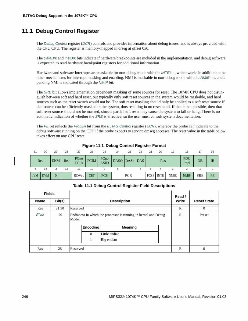
EJTAG Debug Support in the 1074K™ CPU
246 MIPS32® 1074K™ CPU Family Software User’s Manual, Revision 01.03
11.1 Debug Control Register
The Debug Control register (DCR) controls and provides information about debug issues, and is always provided withthe CPU CPU. The register is memory-mapped in drseg at offset 0x0.
The DataBrk and InstBrk bits indicate if hardware breakpoints are included in the implementation, and debug softwareis expected to read hardware breakpoint registers for additional information.
Hardware and software interrupts are maskable for non-debug mode with the INTE bit, which works in addition to theother mechanisms for interrupt masking and enabling. NMI is maskable in non-debug mode with the NMIE bit, and apending NMI is indicated through the NMIP bit.
The SRE bit allows implementation dependent masking of some sources for reset. The 1074K CPU does not distin-guish between soft and hard reset, but typically only soft reset sources in the system would be maskable, and hardsources such as the reset switch would not be. The soft reset masking should only be applied to a soft reset source ifthat source can be efficiently masked in the system, thus resulting in no reset at all. If that is not possible, then thatsoft reset source should not be masked, since a partial soft reset may cause the system to fail or hang. There is noautomatic indication of whether the SRE is effective, so the user must consult system documentation.
The PE bit reflects the ProbEn bit from the EJTAG Control register (ECR), whereby the probe can indicate to thedebug software running on the CPU if the probe expects to service dmseg accesses. The reset value in the table belowtakes effect on any CPU reset.
Figure 11.1 Debug Control Register Format31 30 29 28 27 26 25 24 23 22 21 20 19 18 17 16
Res ENM ResPCnoTCID
PCIMPCnoASID
DASQ DASe DAS ResFDCImpl
DB IB
‘5 14 ‘3 12 11 10 9 8 6 5 4 3 2 1 0
IVM DVM 0 RDVec CBT PCS PCR PCSE INTE NMIE NMIP SRE PE
Table 11.1 Debug Control Register Field Descriptions
Fields
DescriptionRead /Write Reset StateName Bit(s)
Res 31:30 Reserved R 0
ENM 29 Endianess in which the processor is running in kernel and DebugMode:
R Preset
Res 28 Reserved R 0
Encoding Meaning
0 Little endian
1 Big endian
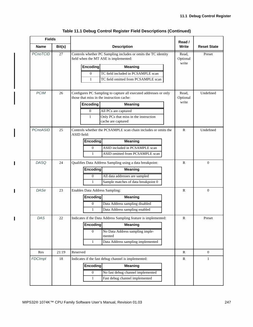
11.1 Debug Control Register
MIPS32® 1074K™ CPU Family Software User’s Manual, Revision 01.03 247
PCnoTCID 27 Controls whether PC Sampling includes or omits the TC identityfield when the MT ASE is implemented:
Read,Optional
write
Preset
PCIM 26 Configures PC Sampling to capture all executed addresses or onlythose that miss in the instruction cache:
Read,Optional
write
Undefined
PCnoASID 25 Controls whether the PCSAMPLE scan chain includes or omits theASID field:
R Undefined
DASQ 24 Qualifies Data Address Sampling using a data breakpoint: R 0
DASe 23 Enables Data Address Sampling: R 0
DAS 22 Indicates if the Data Address Sampling feature is implemented: R Preset
Res 21:19 Reserved R 0
FDCImpl 18 Indicates if the fast debug channel is implemented: R 1
Table 11.1 Debug Control Register Field Descriptions (Continued)
Fields
DescriptionRead /Write Reset StateName Bit(s)
Encoding Meaning
0 TC field included in PCSAMPLE scan
1 TC field omitted from PCSAMPLE scan
Encoding Meaning
0 All PCs are captured
1 Only PCs that miss in the instructioncache are captured
Encoding Meaning
0 ASID included in PCSAMPLE scan
1 ASID omitted from PCSAMPLE scan
Encoding Meaning
0 All data addresses are sampled
1 Sample matches of data breakpoint 0
Encoding Meaning
0 Data Address sampling disabled
1 Data Address sampling enabled
Encoding Meaning
0 No Data Address sampling imple-mented
1 Data Address sampling implemented
Encoding Meaning
0 No fast debug channel implemented
1 Fast debug channel implemented
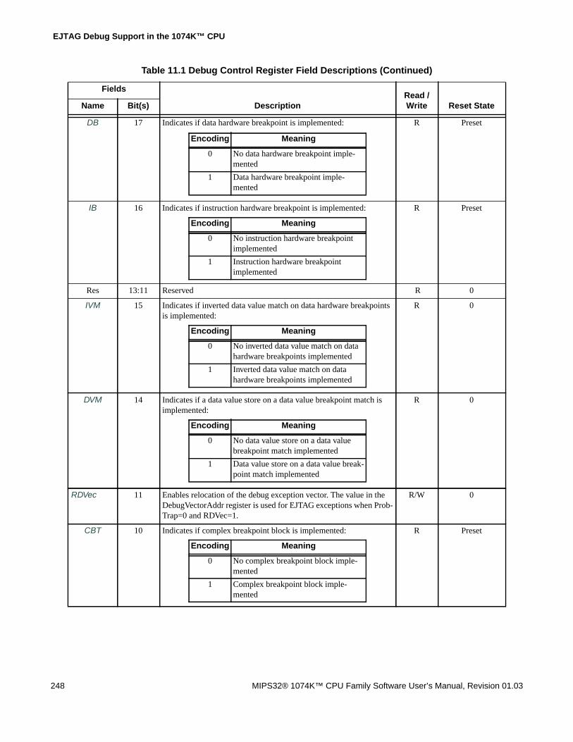
EJTAG Debug Support in the 1074K™ CPU
248 MIPS32® 1074K™ CPU Family Software User’s Manual, Revision 01.03
DB 17 Indicates if data hardware breakpoint is implemented: R Preset
IB 16 Indicates if instruction hardware breakpoint is implemented: R Preset
Res 13:11 Reserved R 0
IVM 15 Indicates if inverted data value match on data hardware breakpointsis implemented:
R 0
DVM 14 Indicates if a data value store on a data value breakpoint match isimplemented:
R 0
RDVec 11 Enables relocation of the debug exception vector. The value in theDebugVectorAddr register is used for EJTAG exceptions when Prob-Trap=0 and RDVec=1.
R/W 0
CBT 10 Indicates if complex breakpoint block is implemented: R Preset
Table 11.1 Debug Control Register Field Descriptions (Continued)
Fields
DescriptionRead /Write Reset StateName Bit(s)
Encoding Meaning
0 No data hardware breakpoint imple-mented
1 Data hardware breakpoint imple-mented
Encoding Meaning
0 No instruction hardware breakpointimplemented
1 Instruction hardware breakpointimplemented
Encoding Meaning
0 No inverted data value match on datahardware breakpoints implemented
1 Inverted data value match on datahardware breakpoints implemented
Encoding Meaning
0 No data value store on a data valuebreakpoint match implemented
1 Data value store on a data value break-point match implemented
Encoding Meaning
0 No complex breakpoint block imple-mented
1 Complex breakpoint block imple-mented

11.1 Debug Control Register
MIPS32® 1074K™ CPU Family Software User’s Manual, Revision 01.03 249
PCS 9 Indicates if the PC Sampling feature is implemented.: R Preset
PCR 8:6 PC Sampling Rate: Values from 0 to 7 map to 25 to 212 cyclesrespectively. That is, a PC sample is written out every 32, 64, 128,256, 512, 1024, 2048, or 4096 cycles. The external probe or softwareis allowed to set this value to the desired sample rate
R/W 7
PCSE 5 Indicates if PC Sampling is enabled:
This bit is set to 0 following Reset. It must be set by software toenable PC sampling.
R/W 0
INTE 4 Interrupt Enable in Normal Mode. This bit provides the hardwareand software interrupt enable for non-debug mode, in addition toother masking mechanisms in conjunction with other disable mecha-nisms:
R/W 1
NMIE 3 Non-Maskable Interrupt (NMI) enable for Non-Debug Mode: R/W 1
NMIP 2 Indication for pending NMI: R 0
Table 11.1 Debug Control Register Field Descriptions (Continued)
Fields
DescriptionRead /Write Reset StateName Bit(s)
Encoding Meaning
0 No PC Sampling implemented
1 PC Sampling implemented
Encoding Meaning
0 PC Sampling not enabled
1 PC Sampling enabled
Encoding Meaning
0 Interrupt disabled
1 Interrupt enabled depending on otherenabling mechanisms
Encoding Meaning
0 NMI disabled
1 NMI enabled
Encoding Meaning
0 No NMI pending
1 NMI pending

EJTAG Debug Support in the 1074K™ CPU
250 MIPS32® 1074K™ CPU Family Software User’s Manual, Revision 01.03
11.2 Hardware Breakpoints
Hardware breakpoints provide for the comparison by hardware of executed instructions and data load/store transac-tions. It is possible to set instruction breakpoints on addresses even in ROM area,. Data breakpoints can be set tocause a debug exception on a specific data transaction. Instruction and data hardware breakpoints are alike in manyaspects, and are thus described in parallel in the following. The term hardware is not applied to breakpoint, unlessrequired to distinguish it from software breakpoint.
There are two types of simple hardware breakpoints implemented in the 1074K CPU: instruction breakpoints anddata breakpoints.
A CPU may be configured with the following breakpoint options:
• No breakpoints
• Four instruction and two data breakpoints
11.2.1 Features of Instruction Breakpoint
Instruction breaks occur on instruction fetch operations and the break is set on the virtual address on the bus betweenthe CPU and the instruction cache. Instruction breaks can also be made on the ASID value used by the TLB-basedMMU. Finally, a mask can be applied to the virtual address to set breakpoints on a range of instructions.
SRE 1 Soft Reset EnableThis bit allows the system to mask soft resets. The CPU does notinternally mask resets. Rather the state of this bit appears on theEJ_SRstE external output signal, allowing the system to mask softresets if desired.
Bit is read-only (R) and reads as zero if not implemented.
R/W 1
PE 0 Probe EnableThis bit reflects the value of the ProbEn bit in the EJTAG Controlregister:
Bit is read-only (R) and reads as zero if not implemented.
R Same value asProbEn in ECR(see Table 11.25)
Table 11.1 Debug Control Register Field Descriptions (Continued)
Fields
DescriptionRead /Write Reset StateName Bit(s)
Encoding Meaning
0 Soft reset masked for soft reset sourcesdependent on implementation
1 Soft reset is fully enabled
Encoding Meaning
0 No access should occur to the dmsegsegment
1 Probe services accesses to the dmsegsegment

11.2 Hardware Breakpoints
MIPS32® 1074K™ CPU Family Software User’s Manual, Revision 01.03 251
Instruction breakpoints compare the virtual address of the executed instructions (PC) and the ASID with the registersfor each instruction breakpoint including masking of address and ASID. When an instruction breakpoint matches, adebug exception and/or a trigger is generated. An internal bit in the instruction breakpoint registers is set to indicatethat the match occurred.
11.2.2 Features of Data Breakpoint
Data breakpoints occur on load/store transactions. Breakpoints are set on virtual address and ASID values, similar tothe Instruction breakpoint. Data breakpoints can be set on a load, a store or both. Data breakpoints can also be setbased on the value of the load/store operation. Finally, masks can be applied to both the virtual address and theload/store value.
Data breakpoints compare the transaction type (TYPE), which may be load or store, the virtual address of the transac-tion (ADDR), the ASID, accessed bytes (BYTELANE) and data value (DATA), with the registers for each data break-point including masking or qualification on the transaction properties. When a data breakpoint matches, a debugexception and/or a trigger is generated, and an internal bit in the data breakpoint registers is set to indicate that thematch occurred. The match is precise in that the debug exception or trigger occurs on the instruction that caused thebreakpoint to match.
11.2.3 Instruction Breakpoint Registers Overview
The register with implementation indication and status for instruction breakpoints in general is shown in Table 11.2.
The four instruction breakpoints are numbered 0 to 3 for registers and breakpoints, and the number is indicated by n.The registers for each breakpoint are shown in Table 11.3.
11.2.4 Data Breakpoint Registers Overview
The register with implementation indication and status for data breakpoints in general is shown in Table 11.4.
Table 11.2 Overview of Status Register for Instruction Breakpoints
Register Mnemonic Register Name and Description
IBS Instruction Breakpoint Status
Table 11.3 Overview of Registers for Each Instruction Breakpoint
Register Mnemonic Register Name and Description
IBAn Instruction Breakpoint Address n
IBMn Instruction Breakpoint Address Mask n
IBASIDn Instruction Breakpoint ASID n
IBCn Instruction Breakpoint Control n
Table 11.4 Overview of Status Register for Data Breakpoints
Register Mnemonic Register Name and Description
DBS Data Breakpoint Status

EJTAG Debug Support in the 1074K™ CPU
252 MIPS32® 1074K™ CPU Family Software User’s Manual, Revision 01.03
The two data breakpoints are numbered 0 and 1 for registers and breakpoints, and the number is indicated by n. Theregisters for each breakpoint are shown in Table 11.5.
11.2.5 Conditions for Matching Breakpoints
A number of conditions must be fulfilled in order for a breakpoint to match on an executed instruction or a data trans-action, and the conditions for matching instruction and data breakpoints are described below. The breakpoints onlymatch for instructions executed in non-debug mode, thus never on instructions executed in debug mode.
The match of an enabled breakpoint can either generate a debug exception or a trigger indication. The BE and/or TEbits in the IBCn or DBCn registers are used to enable the breakpoints.
Debug software should not configure breakpoints to compare on an ASID value unless a TLB is present in the imple-mentation.
11.2.5.1 Conditions for Matching Instruction Breakpoints
When an instruction breakpoint is enabled, that breakpoint is evaluated for the address of every executed instructionin non-debug mode, including execution of instructions at an address causing an address error on an instruction fetch.The breakpoint is not evaluated on instructions from a speculative fetch or execution, nor for addresses which areunaligned with an executed instruction.
A breakpoint match depends on the virtual address of the executed instruction (PC) which can be masked at bit level,and match also can include an optional compare of ASID. The registers for each instruction breakpoint have the val-ues and mask used in the compare, and the equation that determines the match is shown below in C-like notation.
IB_match =( ! IBCnASIDuse || ( ASID == IBASIDnASID ) ) &&( <all 1’s> == ( IBMnIBM | ~ ( PC ^ IBAnIBA ) &&( (IBMnISAM | ~(ISAMode ^ IBAnISA))) )
The match indication for instruction breakpoints is always precise, i.e. indicated on the instruction causing theIB_match to be true.
11.2.5.2 Conditions for Matching Data Breakpoints
When a data breakpoint is enabled, that breakpoint is evaluated for every data transaction due to a load/store instruc-tion executed in non-debug mode, including load/store for coprocessor, and transactions causing an address error ondata access. The breakpoint is not evaluated due to a PREF instruction or other transactions which are not part ofexplicit load/store transactions in the execution flow, nor for addresses which are not the explicit load/store source ordestination address.
Table 11.5 Overview of Registers for Each Data Breakpoint
Register Mnemonic Register Name and Description
DBAn Data Breakpoint Address n
DBMn Data Breakpoint Address Mask n
DBASIDn Data Breakpoint ASID n
DBCn Data Breakpoint Control n
DBVn Data Breakpoint Value n

11.2 Hardware Breakpoints
MIPS32® 1074K™ CPU Family Software User’s Manual, Revision 01.03 253
A breakpoint match depends on the transaction type (TYPE) as load or store, the address, and optionally the datavalue of a transaction. The registers for each data breakpoint have the values and mask used in the compare, and theequation that determines the match is shown below in C-like notation.
The overall match equation is the DB_match.
DB_match =( ( ( TYPE == load ) && ! DBCnNoLB ) ||( ( TYPE == store ) && ! DBCnNoSB ) ) &&
DB_addr_match && ( DB_no_value_compare || DB_value_match )
The match on the address part, DB_addr_match, depends on the virtual address of the transaction (ADDR), the ASIDvalue, and the accessed bytes (BYTELANE) where BYTELANE[0] is 1 only if the byte at bits [7:0] on the bus isaccessed, and BYTELANE[1] is 1 only if the byte at bits [15:8] is accessed, etc. The DB_addr_match is shownbelow.
DB_addr_match =( ! DBCnASIDuse || ( ASID == DBASIDnASID ) ) &&( <all 1’s> == ( DBMnDBM | ~ ( ADDR ^ DBAnDBA ) ) ) &&( <all 0’s> != ( ~ BAI & BYTELANE ) )
The size of DBCnBAI and BYTELANE is 8 bits. They are 8 bits to allow for data value matching on doubleword float-ing point loads and stores. For non-doubleword loads and stores, only the lower 4 bits will be used.
Data value compare is included in the match condition for the data breakpoint depending on the bytes (BYTELANEas described above) accessed by the transaction, and the contents of breakpoint registers. The DB_no_value_compareis shown below.
DB_no_value_compare =( <all 1’s> == ( DBCnBLM | DBCnBAI | ~ BYTELANE ) )
The size of DBCnBLM, DBCnBAI and BYTELANE is 8 bits.
In case a data value compare is required, DB_no_value_compare is false, then the data value from the data bus(DATA) is compared and masked with the registers for the data breakpoint. The endianess is not considered in thesematch equations for value, as the compare uses the data bus value directly, thus debug software is responsible forsetup of the breakpoint corresponding with endianess.
DB_value_match =( ( DATA[7:0] == DBVnDBV[7:0] ) || !BYTELANE[0] || DBCnBLM[0] || DBCnBAI[0] ) &&( ( DATA[15:8] == DBVnDBV[15:8] ) || !BYTELANE[1] || DBCnBLM[1] || DBCnBAI[1] ) &&( ( DATA[23:16] == DBVnDBV[23:16] ) || !BYTELANE[2] || DBCnBLM[2] || DBCnBAI[2] )&&( ( DATA[31:24] == DBVnDBV[31:24] ) || !BYTELANE[3] || DBCnBLM[3] || DBCnBAI[3] )&&( ( DATA[39:32] == DBVnDBV[39:32] ) || !BYTELANE[4] || DBCnBLM[4] || DBCnBAI[4] )&&( ( DATA[47:40] == DBVnDBV[47:40] ) || !BYTELANE[5] || DBCnBLM[5] || DBCnBAI[5] )&&( ( DATA[55:48] == DBVnDBV[55:48] ) || !BYTELANE[6] || DBCnBLM[6] || DBCnBAI[6] )&&( ( DATA[63:56] == DBVnDBV[63:56] ) || !BYTELANE[7] || DBCnBLM[7] || DBCnBAI[7] ))
The match for a data breakpoint without value compare is always precise, since the match expression is fully evalu-ated at the time the load/store instruction is executed. A true DB_match can thereby be indicated on the very sameinstruction causing the DB_match to be true. The match for data breakpoints with value compare is always imprecise.

EJTAG Debug Support in the 1074K™ CPU
254 MIPS32® 1074K™ CPU Family Software User’s Manual, Revision 01.03
11.2.6 Debug Exceptions from Breakpoints
Instruction and data breakpoints may be set up to generate a debug exception when the match condition is true, asdescribed below.
11.2.6.1 Debug Exception by Instruction Breakpoint
If the breakpoint is enabled by BE bit in the IBCn register, then a debug instruction break exception occurs if theIB_match equation is true. The corresponding BS[n] bit in the IBS register is set when the breakpoint generates thedebug exception.
The debug instruction break exception is always precise, so the DEPC register and DBD bit in the Debug register pointto the instruction that caused the IB_match equation to be true.
The instruction receiving the debug exception does not update any registers due to the instruction, nor does any loador store by that instruction occur. Thus a debug exception from a data breakpoint can not occur for instructions receiv-ing a debug instruction break exception.
The debug handler usually returns to the instruction causing the debug instruction break exception, whereby theinstruction is executed. Debug software is responsible for disabling the breakpoint when returning to the instruction,otherwise the debug instruction break exception reoccurs.
11.2.6.2 Debug Exception by Data Breakpoint
If the breakpoint is enabled by BE bit in the DBCn register, then a debug exception occurs when the DB_match condi-tion is true. The corresponding BS[n] bit in the DBS register is set when the breakpoint generates the debug exception.A matching data breakpoint generates either a precise or imprecise debug exception
Debug Data Break Load/Store Exception as a Precise Debug Exception
A precise debug data break exception occurs when a data breakpoint without value compare indicates a match. In thiscase the DEPC register and DBD bit in the Debug register points to the instruction that caused the DB_match equationto be true.
The instruction causing the debug data break exception does not update any registers due to the instruction, and thefollowing applies to the load or store transaction causing the debug exception:
• A store transaction is not allowed to complete the store to the memory system.
• A load transaction with no data value compare, i.e. where the DB_no_value_compare is true for the match, is notallowed to complete the load.
The result of this is that the load or store instruction causing the debug data break exception appears as not executed.

11.2 Hardware Breakpoints
MIPS32® 1074K™ CPU Family Software User’s Manual, Revision 01.03 255
If both data breakpoints without and with data value compare would match the same transaction and generate a debugexception, then the rules shown in Table 11.6 apply with respect to updating the BS[n] bits.
Any BS[n] bit set prior to the match and debug exception are kept set, since BS[n] bits are only cleared by debug soft-ware.
The debug handler usually returns to the instruction causing the debug data break exception, whereby the instructionis re-executed. Debug software is responsible for disabling breakpoints when returning to the instruction; otherwisethe debug data break exception will reoccur.
Debug Data Break Load/Store Exception as an Imprecise Debug Exception
An Debug Data Break Load/Store Imprecise exception occurs when a data breakpoint indicates an imprecise match.Imprecise matches are generated when data value compare is used. In this case, the DEPC register and DBD bit in theDebug register point to an instruction later in the execution flow rather than at the load/store instruction that causedthe DB_match equation to be true.
The load/store instruction causing the Debug Data Break Load/Store Imprecise exception always updates the destina-tion register and completes the access to the external memory system. Therefore this load/store instruction is notre-executed on return from the debug handler, because the DEPC register and DDBSImpr bit do not point to thatinstruction.
Several imprecise data breakpoints can be pending at a given time, if the bus system supports multiple outstandingdata accesses. The breakpoints are evaluated as the accesses finalize, and a Debug Data Break Load/Store Impreciseexception is generated only for the first one matching. Both the first and succeeding matches cause correspondingDDBSImpr bits and DDBLImpr/DDBSImpr in the Debug register to be set, but no debug exception is generated for suc-ceeding matches because the processor is already in Debug Mode. Similarly, if a debug exception had alreadyoccurred at the time of the first match (for example, due to a precise debug exception), then all matches cause the cor-responding BS bits and DDBLImpr/DDBSImpr to be set, but no debug exception is generated because the processor isalready in Debug Mode.
Table 11.6 Rules for Update of BS Bits on Data Breakpoint Exceptions
Instruction
Breakpoints that MatchUpdate of BS Bits for Matching Data
Breakpoints
Without ValueCompare With Value Compare
Without ValueCompare With Value Compare
Load/Store One or more None BS bits set for all (No matching break-points)
Load One or more One or more BS bits set for all Unchanged BS bits sinceload of data value does
not occur so match of thebreakpoint cannot be
determined
Load None One or more (No matching break-points)
BS bits set for all
Store One or more One or more BS bits set for all BS bits set for all
Store None One or more (No matching break-points)
BS bits set for all

EJTAG Debug Support in the 1074K™ CPU
256 MIPS32® 1074K™ CPU Family Software User’s Manual, Revision 01.03
The SYNC instruction, followed by appropriate spacing must be executed before the DDBSImpr bits andDDBSImpr/DDBSImpr bits are accessed for read or write. This delay ensures that these bits are fully updated.
Any DDBSImpr bit set prior to the match and debug exception are kept set, because only debug software can clear theDDBSImpr bits.
11.2.7 Breakpoint used as TriggerPoint
Both instruction and data hardware breakpoints can be setup by software so a matching breakpoint does not generatea debug exception, but only an indication through the BS[n] bit. The TE bit in the IBCn or DBCn register controls if aninstruction or data breakpoint is used as a so-called triggerpoint. The triggerpoints are, like breakpoints, only com-pared for instructions executed in non-debug mode.
The BS[n] bit in the IBS or DBS register is set when the respective IB_match or DB_match bit is true.
11.2.8 Instruction Breakpoint Registers
The registers for instruction breakpoints are described below. These registers have implementation information andare used to set up the instruction breakpoints. All registers are in drseg, and the addresses are shown in Table 11.7.
An example of some of the registers; IBA0 is at offset 0x1100 and IBC2 is at offset 0x1318.
11.2.8.1 Instruction Breakpoint Status (IBS) Register
Compliance Level: Implemented only if instruction breakpoints are implemented.
The Instruction Breakpoint Status (IBS) register holds implementation and status information about the instructionbreakpoints.
The ASID applies to all the instruction breakpoints.
Figure 11.2 IBS Register Format
Table 11.7 Addresses for Instruction Breakpoint Registers
Offset in drsegRegister
Mnemonic Register Name and Description
0x1000 IBS Instruction Breakpoint Status
0x1100 + n * 0x100 IBAn Instruction Breakpoint Address n
0x1108 + n * 0x100 IBMn Instruction Breakpoint Address Mask n
0x1110 + n * 0x100 IBASIDn Instruction Breakpoint ASID n
0x1118 + n * 0x100 IBCn Instruction Breakpoint Control n
n is breakpoint number in range 0 to 3
31 30 29 28 27 24 23 4 3 0
Res ASIDsup Res BCN Res BS

11.2 Hardware Breakpoints
MIPS32® 1074K™ CPU Family Software User’s Manual, Revision 01.03 257
11.2.8.2 Instruction Breakpoint Address n (IBAn) Register
Compliance Level: Implemented only for implemented instruction breakpoints.
The Instruction Breakpoint Address n (IBAn) register has the address used in the condition for instruction breakpointn.
Figure 11.3 IBAn Register Format
11.2.8.3 Instruction Breakpoint Address Mask n (IBMn) Register
Compliance Level: Implemented only for implemented instruction breakpoints.
The Instruction Breakpoint Address Mask n (IBMn) register has the mask for the address compare used in the condi-tion for instruction breakpoint n.
Table 11.8 IBS Register Field Descriptions
FieldsDescription Read /
Write Reset StateName Bit(s)
Res 31 Must be written as zero; returns zero on read. R 0
ASIDsup 30 Indicates that ASID compare is supported in instruction break-points.
R Fixed MMU - 0TLB - 1
Res 29:28 Must be written as zero; returns zero on read. R 0
BCN 27:24 Number of instruction breakpoints implemented. R 4
Res 23:4 Must be written as zero; returns zero on read. R 0
31 1 0
IBA ISA
Table 11.9 IBAn Register Field Descriptions
Fields
DescriptionRead /Write Reset StateName Bit(s)
IBA 31:1 Instruction breakpoint address for condition. R/W Undefined
ISA 0 Instruction breakpoint ISA mode for condition R/W Undefined
Encoding Meaning
0 No ASID compare.
1 ASID compare (IBASIDn registerimplemented).

EJTAG Debug Support in the 1074K™ CPU
258 MIPS32® 1074K™ CPU Family Software User’s Manual, Revision 01.03
Figure 11.4 IBMn Register Format
11.2.8.4 Instruction Breakpoint ASID n (IBASIDn) Register
Compliance Level: Implemented only for implemented instruction breakpoints.
For processors with a TLB based MMU, this register is used to define an ASID value to be used in the match expres-sion. For CPUs with an FM MMU, this register is reserved and reads as 0.
Figure 11.5 IBASIDn Register Format
11.2.8.5 Instruction Breakpoint Control n (IBCn) Register
Compliance Level: Implemented only for implemented instruction breakpoints.
31 1 0
IBM ISAM
Table 11.10 IBMn Register Field Descriptions
Fields
DescriptionRead /Write Reset StateName Bit(s)
IBM 31:1 Instruction breakpoint address mask for condition: R/W Undefined
ISAM 0 Instruction breakpoint ISA mode mask for condition: R/W Undefined
31 8 7 0
Res ASID
Table 11.11 IBASIDn Register Field Descriptions
Fields
DescriptionRead /Write Reset StateName Bit(s)
Res 31:8 Must be written as zero; returns zero on read. R 0
ASID 7:0 Instruction breakpoint ASID value for a compare. R/W Undefined
Encoding Meaning
0 Corresponding address bit not masked.
1 Corresponding address bit masked.
Encoding Meaning
0 ISA mode considered for match condi-tion
1 ISA mode masked

11.2 Hardware Breakpoints
MIPS32® 1074K™ CPU Family Software User’s Manual, Revision 01.03 259
The Instruction Breakpoint Control n (IBCn) register controls the setup of instruction breakpoint n.
Figure 11.6 IBCn Register Format31 24 23 22 21 3 2 1 0
ResASIDuse
ResRes TE Res BE
Table 11.12 BCn Register Field Descriptions
Fields
DescriptionRead /Write Reset StateName Bits
Res 31:24 Must be written as zero; returns zero on read. R 0
ASIDuse 23 Use ASID value in compare for instruction breakpoint n: R/W Undefined
Res 22 Must be written as zero; returns zero on read. R 0
Res 21:3 Must be written as zero; returns zero on read. R 0
TE 2 Use instruction breakpoint n as triggerpoint: R/W 0
Res 1 Must be written as zero; returns zero on read. R 0
BE 0 Use instruction breakpoint n as breakpoint: R/W 0
Encoding Meaning
0 Don’t use ASID value in compare
1 Use ASID value in compare
Encoding Meaning
0 Don’t use it as triggerpoint
1 Use it as triggerpoint
Encoding Meaning
0 Don’t use it as breakpoint
1 Use it as breakpoint

EJTAG Debug Support in the 1074K™ CPU
260 MIPS32® 1074K™ CPU Family Software User’s Manual, Revision 01.03
11.2.9 Data Breakpoint Registers
The registers for data breakpoints are described below. These registers have implementation information and are usedthe setup the data breakpoints. All registers are in drseg, and the addresses are shown in Table 11.13.
An example of some of the registers; DBM0 is at offset 0x2108 and DBV1 is at offset 0x2220.
11.2.9.1 Data Breakpoint Status (DBS) Register
Compliance Level: Implemented if data breakpoints are implemented.
The Data Breakpoint Status (DBS) register contains implementation and status information about the data break-points.
The ASIDsup field indicates whether ASID compares are supported.
Figure 11.7 DBS Register Format
Table 11.13 Addresses for Data Breakpoint Registers
Offset in drsegRegister
Mnemonic Register Name and Description
0x2000 DBS Data Breakpoint Status
0x2100 + 0x100 * n DBAn Data Breakpoint Address n
0x2108 + 0x100 * n DBMn Data Breakpoint Address Mask n
0x2110 + 0x100 * n DBASIDn Data Breakpoint ASID n
0x2118 + 0x100 * n DBCn Data Breakpoint Control n
0x2120 + 0x100 * n DBVn Data Breakpoint Value n
0x2124 + 0x100*n DBVHn Data Breakpoint Value High n
n is breakpoint number as 0 or 1
31 30 29 28 27 24 23 2 1 0
Res ASIDsup Res BCN Res BS
Table 11.14 DBS Register Field Descriptions
Fields
DescriptionRead /Write Reset StateName Bit(s)
Res 31 Must be written as zero; returns zero on read. R 0
ASIDsup 30 Indicates that ASID compares are supported in data breakpoints. R TLB MMU - 1FM MMU - 0
Res 29:28 Must be written as zero; returns zero on read. R 0
BCN 27:24 Number of data breakpoints implemented. R 2
Res 23:2 Must be written as zero; returns zero on read. R 0
Encoding Meaning
0 Not supported
1 Supported

11.2 Hardware Breakpoints
MIPS32® 1074K™ CPU Family Software User’s Manual, Revision 01.03 261
11.2.9.2 Data Breakpoint Address n (DBAn) Register
Compliance Level: Implemented only for implemented data breakpoints.
The Data Breakpoint Address n (DBAn) register has the address used in the condition for data breakpoint n.
Figure 11.8 DBAn Register Format
11.2.9.3 Data Breakpoint Address Mask n (DBMn) Register
Compliance Level: Implemented only for implemented data breakpoints.
The Data Breakpoint Address Mask n (DBMn) register has the mask for the address compare used in the condition fordata breakpoint n.
Figure 11.9 DBMn Register Format
BS 1:0 Break status for breakpoint n is at BS[n], with n from 0 to 1. The bitis set to 1 when the condition for the corresponding breakpoint hasmatched.
R/W0 Undefined
31 0
DBA
Table 11.15 DBAn Register Field Descriptions
Fields
DescriptionRead /Write Reset StateName Bit(s)
DBA 31:0 Data breakpoint address for condition. R/W Undefined
31 0
DBM
Table 11.16 DBMn Register Field Descriptions
Fields
DescriptionRead /Write Reset StateName Bit(s)
DBM 31:0 Data breakpoint address mask for condition: R/W Undefined
Table 11.14 DBS Register Field Descriptions
Fields
DescriptionRead /Write Reset StateName Bit(s)
Encoding Meaning
0 Corresponding address bit not masked
1 Corresponding address bit masked

EJTAG Debug Support in the 1074K™ CPU
262 MIPS32® 1074K™ CPU Family Software User’s Manual, Revision 01.03
11.2.9.4 Data Breakpoint ASID n (DBASIDn) Register
Compliance Level: Implemented only for implemented data breakpoints.
For processors with a TLB based MMU, this register is used to define an ASID value to be used in the match expres-sion. For CPUs with the FM MMU, this register is reserved and reads as 0.
Figure 11.10 DBASIDn Register Format
11.2.9.5 Data Breakpoint Control n (DBCn) Register
Compliance Level: Implemented only for implemented data breakpoints.
The Data Breakpoint Control n (DBCn) register controls the setup of data breakpoint n.
Figure 11.11 DBCn Register Format
31 8 7 0
Res ASID
Table 11.17 DBASIDn Register Field Descriptions
Fields
DescriptionRead /Write Reset StateName Bit(s)
Res 31:8 Must be written as zero; returns zero on read. R 0
ASID 7:0 Data breakpoint ASID value for compares. R/W Undefined
31 24 23 22 21 14 13 12 11 4 3 2 1 0
ResASIDuse
ResBAI NoSB NoLB BLM Res TE Res BE
Table 11.18 DBCn Register Field Descriptions
Fields
DescriptionRead /Write Reset StateName Bits
Res 31:24 Must be written as zero; returns zero on reads. R 0
ASIDuse 23 Use ASID value in compare for data breakpoint n: R/W Undefined
Encoding Meaning
0 Don’t use ASID value in compare
1 Use ASID value in compare

11.2 Hardware Breakpoints
MIPS32® 1074K™ CPU Family Software User’s Manual, Revision 01.03 263
Res 22 Must be written as zero; returns zero on reads R 0
BAI 21:14 Byte access ignore controls ignore of access to a specific byte.BAI[0] ignores access to byte at bits [7:0] of the data bus, BAI[1]ignores access to byte at bits [15:8], etc.
R/W Undefined
NoSB 13 Controls if condition for data breakpoint is not fulfilled on a storetransaction:
R/W Undefined
NoLB 12 Controls if condition for data breakpoint is not fulfilled on a loadtransaction:
R/W Undefined
BLM 11:4 Byte lane mask for value compare on data breakpoint. BLM[0]masks byte at bits [7:0] of the data bus, BLM[1] masks byte at bits[15:8], etc.:
R/W Undefined
Res 3 Must be written as zero; returns zero on reads. R 0
TE 2 Use data breakpoint n as triggerpoint: R/W 0
Res 1 Must be written as zero; returns zero on reads. R 0
Table 11.18 DBCn Register Field Descriptions (Continued)
Fields
DescriptionRead /Write Reset StateName Bits
Encoding Meaning
0 Condition depends on access to corre-sponding byte
1 Access for corresponding byte isignored
Encoding Meaning
0 Condition may be fulfilled on storetransaction
1 Condition is never fulfilled on storetransaction
Encoding Meaning
0 Condition may be fulfilled on loadtransaction
1 Condition is never fulfilled on loadtransaction
Encoding Meaning
0 Compare corresponding byte lane
1 Mask corresponding byte lane
Encoding Meaning
0 Don’t use it as triggerpoint
1 Use it as triggerpoint

EJTAG Debug Support in the 1074K™ CPU
264 MIPS32® 1074K™ CPU Family Software User’s Manual, Revision 01.03
11.2.9.6 Data Breakpoint Value n (DBVn) Register
Compliance Level: Implemented only for implemented data breakpoints.
The Data Breakpoint Value n (DBVn) register has the value used in the condition for data breakpoint n.
Figure 11.12 DBVn Register Format
11.2.9.7 Data Breakpoint Value High n (DBVHn) Register
Compliance Level: Implemented only for implemented data breakpoints.
The Data Breakpoint Value High n (DBVHn) register has the value used in the condition for data breakpoint n.
Figure 11.13 DBVHn Register Format
BE 0 Use data breakpoint n as breakpoint: R/W 0
31 0
DBV
Table 11.19 DBVn Register Field Descriptions
Fields
DescriptionRead /Write Reset StateName Bit(s)
DBV 31:0 Data breakpoint value for condition. R/W Undefined
31 0
DBVH
Table 11.18 DBCn Register Field Descriptions (Continued)
Fields
DescriptionRead /Write Reset StateName Bits
Encoding Meaning
0 Don’t use it as breakpoint
1 Use it as breakpoint

11.3 Test Access Port (TAP)
MIPS32® 1074K™ CPU Family Software User’s Manual, Revision 01.03 265
11.3 Test Access Port (TAP)
The following main features are supported by the TAP module:
• 5-pin industry standard JTAG Test Access Port (TCK, TMS, TDI, TDO, TRST_N) interface which is compatiblewith IEEE Std. 1149.1.
• Target chip and EJTAG feature identification available through the Test Access Port (TAP) controller.
• The processor can access external memory on the EJTAG Probe serially through the EJTAG pins. This isachieved through Processor Access (PA), and is used to eliminate the use of the system memory for debug rou-tines.
• Support for both ROM based debugger and debugging both through TAP.
11.3.1 EJTAG Internal and External Interfaces
The external interface of the EJTAG module consists of the 5 signals defined by the IEEE standard.
Table 11.20 DBVHn Register Field Descriptions
Fields
DescriptionRead /Write Reset StateName Bit(s)
DBVH 31:0 Data breakpoint value high for condition. This register provides thehigh order bits [63:32] for data value on double-word floating pointloads and stores.
R/W Undefined
Table 11.21 EJTAG Interface Pins
Pin Type Description
TCK I Test Clock InputInput clock used to shift data into or out of the Instruction or data registers. The TCK clock isindependent of the processor clock, so the EJTAG probe can drive TCK independently of theprocessor clock frequency.The CPU signal for this is called EJ_TCK
TMS I Test Mode Select InputThe TMS input signal is decoded by the TAP controller to control test operation. TMS is sam-pled on the rising edge of TCK.The CPU signal for this is called EJ_TMS
TDI I Test Data InputSerial input data (TDI) is shifted into the Instruction register or data registers on the risingedge of the TCK clock, depending on the TAP controller state.The CPU signal for this is called EJ_TDI
TDO O Test Data OutputSerial output data is shifted from the Instruction or data register to the TDO pin on the fallingedge of the TCK clock. When no data is shifted out, the TDO is 3-stated.The CPU signal for this is called EJ_TDO with output enable controlled by EJ_TDOzstate.

EJTAG Debug Support in the 1074K™ CPU
266 MIPS32® 1074K™ CPU Family Software User’s Manual, Revision 01.03
11.3.2 Test Access Port Operation
The TAP controller is controlled by the Test Clock (TCK) and Test Mode Select (TMS) inputs. These two inputs deter-mine whether an instruction register scan or data register scan is performed. The TAP consists of a small controller,driven by the TCK input, which responds to the TMS input as shown in the state diagram in Figure 11.14. The TAPuses both clock edges of TCK. TMS and TDI are sampled on the rising edge of TCK, while TDO changes on the fallingedge of TCK.
At power-up, the TAP is forced into the Test-Logic-Reset state by a low value on TRST_N. The TAP instruction regis-ter is thereby reset to IDCODE. No other parts of the EJTAG hardware are reset through the Test-Logic-Reset state.
When test access is required, a protocol is applied via the TMS and TCK inputs, causing the TAP to exit theTest-Logic-Reset state and move through the appropriate states. From the Run-Test/Idle state, an Instruction registerscan or a data register scan can be issued to transition the TAP through the appropriate states shown in Figure 11.14.
The states of the data and instruction register scan blocks are mirror images of each other, adding symmetry to theprotocol sequences. The first action that occurs when either block is entered is a capture operation. For the data regis-ters, the Capture-DR state is used to capture (or parallel load) the data into the selected serial data path. In the Instruc-tion register, the Capture-IR state is used to capture status information into the Instruction register.
From the Capture states, the TAP transitions to either the Shift or Exit1 states. Normally the Shift state follows theCapture state so that test data or status information can be shifted out for inspection and new data shifted in. Follow-ing the Shift state, the TAP either returns to the Run-Test/Idle state via the Exit1 and Update states or enters the Pausestate via Exit1. The reason for entering the Pause state is to temporarily suspend the shifting of data through either theData or Instruction Register while a required operation, such as refilling a host memory buffer, is performed. Fromthe Pause state shifting can resume by re-entering the Shift state via the Exit2 state or terminate by entering theRun-Test/Idle state via the Exit2 and Update states.
Upon entering the data or Instruction register scan blocks, shadow latches in the selected scan path are forced to holdtheir present state during the Capture and Shift operations. The data being shifted into the selected scan path is notoutput through the shadow latch until the TAP enters the Update-DR or Update-IR state. The Update state causes theshadow latches to update (or parallel load) with the new data that has been shifted into the selected scan path.
TRST_N I Test Reset Input (Optional pin)The TRST_N pin is an active-low signal for asynchronous reset of the TAP controller andinstruction in the TAP module, independent of the processor logic. The processor is not resetby the assertion of TRST_N.The CPU signal for this is called EJ_TRST_NThis signal is optional, but power-on reset must apply a low pulse on this signal at power-onand then leave it high, in case the signal is not available as a pin on the chip. If available on thechip, then it must be low on the board when the EJTAG debug features are unused by theprobe.
Table 11.21 EJTAG Interface Pins (Continued)
Pin Type Description
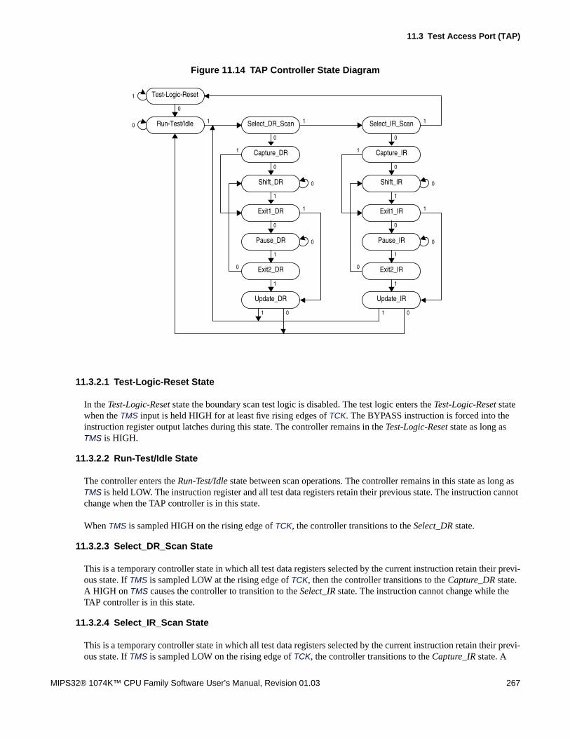
11.3 Test Access Port (TAP)
MIPS32® 1074K™ CPU Family Software User’s Manual, Revision 01.03 267
Figure 11.14 TAP Controller State Diagram
11.3.2.1 Test-Logic-Reset State
In the Test-Logic-Reset state the boundary scan test logic is disabled. The test logic enters the Test-Logic-Reset statewhen the TMS input is held HIGH for at least five rising edges of TCK. The BYPASS instruction is forced into theinstruction register output latches during this state. The controller remains in the Test-Logic-Reset state as long asTMS is HIGH.
11.3.2.2 Run-Test/Idle State
The controller enters the Run-Test/Idle state between scan operations. The controller remains in this state as long asTMS is held LOW. The instruction register and all test data registers retain their previous state. The instruction cannotchange when the TAP controller is in this state.
When TMS is sampled HIGH on the rising edge of TCK, the controller transitions to the Select_DR state.
11.3.2.3 Select_DR_Scan State
This is a temporary controller state in which all test data registers selected by the current instruction retain their previ-ous state. If TMS is sampled LOW at the rising edge of TCK, then the controller transitions to the Capture_DR state.A HIGH on TMS causes the controller to transition to the Select_IR state. The instruction cannot change while theTAP controller is in this state.
11.3.2.4 Select_IR_Scan State
This is a temporary controller state in which all test data registers selected by the current instruction retain their previ-ous state. If TMS is sampled LOW on the rising edge of TCK, the controller transitions to the Capture_IR state. A
Shift_IR
Select_IR_Scan
Capture_IR
Exit1_IR
Pause_IR
Exit2_IR
Update_IR
1
0
0
0
0
0
0
1
1
1
1
1
1
1
0
Shift_DR
Select_DR_Scan
Capture_DR
Exit1_DR
Pause_DR
Exit2_DR
Update_DR
0
0
0
0
0
0
1
1
1
1
1
1
1
0
Test-Logic-Reset
Run-Test/Idle
0
1
0

EJTAG Debug Support in the 1074K™ CPU
268 MIPS32® 1074K™ CPU Family Software User’s Manual, Revision 01.03
HIGH on TMS causes the controller to transition to the Test-Reset-Logic state. The instruction cannot change whilethe TAP controller is in this state.
11.3.2.5 Capture_DR State
In this state the boundary scan register captures the value of the register addressed by the Instruction register, and thevalue is then shifted out in the Shift_DR. If TMS is sampled LOW at the rising edge of TCK, the controller transitionsto the Shift_DR state. A HIGH on TMS causes the controller to transition to the Exit1_DR state. The instruction can-not change while the TAP controller is in this state.
11.3.2.6 Shift_DR State
In this state the test data register connected between TDI and TDO as a result of the current instruction shifts data onestage toward its serial output on the rising edge of TCK. If TMS is sampled LOW on the rising edge of TCK, the con-troller remains in the Shift_DR state. A HIGH on TMS causes the controller to transition to the Exit1_DR state. Theinstruction cannot change while the TAP controller is in this state.
11.3.2.7 Exit1_DR State
This is a temporary controller state in which all test data registers selected by the current instruction retain their previ-ous state. If TMS is sampled LOW at the rising edge of TCK, the controller transitions to the Pause_DR state. A HIGHon TMS causes the controller to transition to the Update_DR state which terminates the scanning process. Theinstruction cannot change while the TAP controller is in this state.
11.3.2.8 Pause_DR State
The Pause_DR state allows the controller to temporarily halt the shifting of data through the test data register in theserial path between TDI and TDO. All test data registers selected by the current instruction retain their previous state.If TMS is sampled LOW on the rising edge of TCK, the controller remains in the Pause_DR state. A HIGH on TMScauses the controller to transition to the Exit2_DR state. The instruction cannot change while the TAP controller is inthis state.
11.3.2.9 Exit2_DR State
This is a temporary controller state in which all test data registers selected by the current instruction retain their previ-ous state. If TMS is sampled LOW at the rising edge of TCK, the controller transitions to the Shift_DR state to allowanother serial shift of data. A HIGH on TMS causes the controller to transition to the Update_DR state which termi-nates the scanning process. The instruction cannot change while the TAP controller is in this state.
11.3.2.10 Update_DR State
When the TAP controller is in this state the value shifted in during the Shift_DR state takes effect on the rising edge ofthe TCK for the register indicated by the Instruction register.
If TMS is sampled LOW at the rising edge of TCK, the controller transitions to the Run-Test/Idle state. A HIGH onTMS causes the controller to transition to the Select_DR_Scan state. The instruction cannot change while the TAPcontroller is in this state and all shift register stages in the test data registers selected by the current instruction retaintheir previous state.
11.3.2.11 Capture_IR State
In this state the shift register contained in the Instruction register loads a fixed pattern (000012) on the rising edge ofTCK. The data registers selected by the current instruction retain their previous state.

11.3 Test Access Port (TAP)
MIPS32® 1074K™ CPU Family Software User’s Manual, Revision 01.03 269
If TMS is sampled LOW at the rising edge of TCK, the controller transitions to the Shift_IR state. A HIGH on TMScauses the controller to transition to the Exit1_IR state. The instruction cannot change while the TAP controller is inthis state.
11.3.2.12 Shift_IR State
In this state the instruction register is connected between TDI and TDO and shifts data one stage toward its serial out-put on the rising edge of TCK. If TMS is sampled LOW at the rising edge of TCK, the controller remains in theShift_IR state. A HIGH on TMS causes the controller to transition to the Exit1_IR state.
11.3.2.13 Exit1_IR State
This is a temporary controller state in which all registers retain their previous state. If TMS is sampled LOW at the ris-ing edge of TCK, the controller transitions to the Pause_IR state. A HIGH on TMS causes the controller to transitionto the Update_IR state which terminates the scanning process. The instruction cannot change while the TAP control-ler is in this state and the instruction register retains its previous state.
11.3.2.14 Pause_IR State
The Pause_IR state allows the controller to temporarily halt the shifting of data through the instruction register in theserial path between TDI and TDO. If TMS is sampled LOW at the rising edge of TCK, the controller remains in thePause_IR state. A HIGH on TMS causes the controller to transition to the Exit2_IR state. The instruction cannotchange while the TAP controller is in this state.
11.3.2.15 Exit2_IR State
This is a temporary controller state in which the instruction register retains its previous state. If TMS is sampled LOWat the rising edge of TCK, then the controller transitions to the Shift_IR state to allow another serial shift of data. AHIGH on TMS causes the controller to transition to the Update_IR state which terminates the scanning process. Theinstruction cannot change while the TAP controller is in this state.
11.3.2.16 Update_IR State
The instruction shifted into the instruction register takes effect on the rising edge of TCK.
If TMS is sampled LOW at the rising edge of TCK, the controller transitions to the Run-Test/Idle state. A HIGH onTMS causes the controller to transition to the Select_DR_Scan state.
11.3.3 Test Access Port (TAP) Instructions
The TAP Instruction register allows instructions to be serially input into the device when TAP controller is in theShift-IR state. Instructions are decoded and define the serial test data register path that is used to shift data betweenTDI and TDO during data register scanning.
The Instruction register is a 5-bit register. In the current EJTAG implementation only some instructions have beendecoded; the unused instructions default to the BYPASS instruction.
Table 11.22 Implemented EJTAG Instructions
Value Instruction Function
0x01 IDCODE Select Chip Identification data register
0x03 IMPCODE Select Implementation register
0x08 ADDRESS Select Address register
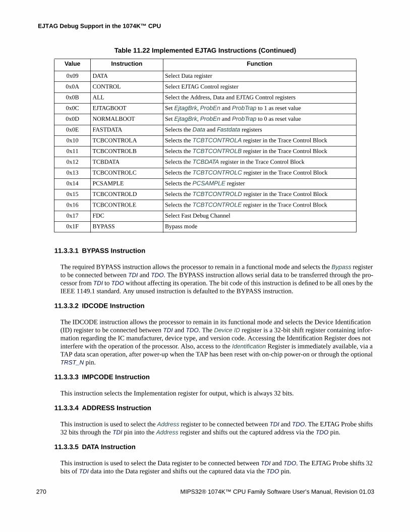
EJTAG Debug Support in the 1074K™ CPU
270 MIPS32® 1074K™ CPU Family Software User’s Manual, Revision 01.03
11.3.3.1 BYPASS Instruction
The required BYPASS instruction allows the processor to remain in a functional mode and selects the Bypass registerto be connected between TDI and TDO. The BYPASS instruction allows serial data to be transferred through the pro-cessor from TDI to TDO without affecting its operation. The bit code of this instruction is defined to be all ones by theIEEE 1149.1 standard. Any unused instruction is defaulted to the BYPASS instruction.
11.3.3.2 IDCODE Instruction
The IDCODE instruction allows the processor to remain in its functional mode and selects the Device Identification(ID) register to be connected between TDI and TDO. The Device ID register is a 32-bit shift register containing infor-mation regarding the IC manufacturer, device type, and version code. Accessing the Identification Register does notinterfere with the operation of the processor. Also, access to the Identification Register is immediately available, via aTAP data scan operation, after power-up when the TAP has been reset with on-chip power-on or through the optionalTRST_N pin.
11.3.3.3 IMPCODE Instruction
This instruction selects the Implementation register for output, which is always 32 bits.
11.3.3.4 ADDRESS Instruction
This instruction is used to select the Address register to be connected between TDI and TDO. The EJTAG Probe shifts32 bits through the TDI pin into the Address register and shifts out the captured address via the TDO pin.
11.3.3.5 DATA Instruction
This instruction is used to select the Data register to be connected between TDI and TDO. The EJTAG Probe shifts 32bits of TDI data into the Data register and shifts out the captured data via the TDO pin.
0x09 DATA Select Data register
0x0A CONTROL Select EJTAG Control register
0x0B ALL Select the Address, Data and EJTAG Control registers
0x0C EJTAGBOOT Set EjtagBrk, ProbEn and ProbTrap to 1 as reset value
0x0D NORMALBOOT Set EjtagBrk, ProbEn and ProbTrap to 0 as reset value
0x0E FASTDATA Selects the Data and Fastdata registers
0x10 TCBCONTROLA Selects the TCBTCONTROLA register in the Trace Control Block
0x11 TCBCONTROLB Selects the TCBTCONTROLB register in the Trace Control Block
0x12 TCBDATA Selects the TCBDATA register in the Trace Control Block
0x13 TCBCONTROLC Selects the TCBTCONTROLC register in the Trace Control Block
0x14 PCSAMPLE Selects the PCSAMPLE register
0x15 TCBCONTROLD Selects the TCBTCONTROLD register in the Trace Control Block
0x16 TCBCONTROLE Selects the TCBTCONTROLE register in the Trace Control Block
0x17 FDC Select Fast Debug Channel
0x1F BYPASS Bypass mode
Table 11.22 Implemented EJTAG Instructions (Continued)
Value Instruction Function

11.3 Test Access Port (TAP)
MIPS32® 1074K™ CPU Family Software User’s Manual, Revision 01.03 271
11.3.3.6 CONTROL Instruction
This instruction is used to select the EJTAG Control register to be connected between TDI and TDO. The EJTAG Probeshifts 32 bits of TDI data into the EJTAG Control register and shifts out the EJTAG Control register bits via TDO.
11.3.3.7 ALL Instruction
This instruction is used to select the concatenation of the Address and Data register, and the EJTAG Control registerbetween TDI and TDO. It can be used in particular if switching instructions in the instruction register takes too manyTCK cycles. The first bit shifted out is bit 0.
Figure 11.15 Concatenation of the EJTAG Address, Data and Control Registers
11.3.3.8 EJTAGBOOT Instruction
When the EJTAGBOOT instruction is given and the Update-IR state is left, then the reset values of the ProbTrap,ProbEn and EjtagBrk bits in the EJTAG Control register are set to 1 after a reset.
This EJTAGBOOT indication is effective until a NORMALBOOT instruction is given, TRST_N is asserted or a risingedge of TCK occurs when the TAP controller is in Test-Logic-Reset state.
It is possible to make the CPU go into debug mode just after a reset, without fetching or executing any instructionsfrom the normal memory area. This can be used for download of code to a system which has no code in ROM.
The Bypass register is selected when the EJTAGBOOT instruction is given.
11.3.3.9 NORMALBOOT Instruction
When the NORMALBOOT instruction is given and the Update-IR state is left, then the reset value of the ProbTrap,ProbEn and EjtagBrk bits in the EJTAG Control register are set to 0 after reset.
The Bypass register is selected when the NORMALBOOT instruction is given.
11.3.3.10 FASTDATA Instruction
This selects the Data and the Fastdata registers at once, as shown in Figure 11.16.
Figure 11.16 TDI to TDO Path When in Shift-DR State and FASTDATA Instruction is Selected
Address 0
Data 0
EJTAG Control 0 TDO
TDI
TDI Data TDOFastdata0

EJTAG Debug Support in the 1074K™ CPU
272 MIPS32® 1074K™ CPU Family Software User’s Manual, Revision 01.03
11.3.3.11 TCBCONTROLA Instruction
This instruction is used to select the TCBCONTROLA register to be connected between TDI and TDO. This register isonly implemented if the Trace unit is present. If no TRU is present, this instruction will select the Bypass register.
11.3.3.12 TCBCONTROLB Instruction
This instruction is used to select the TCBCONTROLB register to be connected between TDI and TDO. This register isonly implemented if the Trace unit is present. If no TRU is present, then this instruction will select the Bypass regis-ter.
11.3.3.13 TCBCONTROLC Instruction
This instruction is used to select the TCBCONTROLC register to be connected between TDI and TDO. This register isonly implemented if the Trace unit is present. If no TRU is present, then this instruction will select the Bypass regis-ter.
11.3.3.14 TCBCONTROLE Instruction
This instruction is used to select the TCBCONTROLE register to be connected between TDI and TDO. This register isonly implemented if the Trace unit is present. If no TRU is present, then this instruction will select the Bypass regis-ter.
11.3.3.15 TCBDATA Instruction
This instruction is used to select the TCBDATA register to be connected between TDI and TDO. This register is onlyimplemented if the Trace unit is present. If no TRU is present, then this instruction will select the Bypass register. Itshould be noted that the TCBDATA register is only an access register to other TCB registers. The width of theTCBDATA register is dependent on the specific TCB register.
11.3.3.16 PCSAMPLE Instruction
This instruction is used to select the PCSAMPLE register to be connected between TDI and TDO. This register isalways implemented.
11.3.3.17 FDC Instruction
This instruction is used to select the Fast Debug Channel register to be connected between TDI and TDO. This registeris always implemented.
11.4 EJTAG TAP Registers
The EJTAG TAP Module has one Instruction register and a number of Data registers, all of which are accessiblethrough the TAP:
11.4.1 Instruction Register
The Instruction register is accessed when the TAP receives an Instruction register scan protocol. During an Instructionregister scan operation, the TAP controller selects the output of the Instruction register to drive the TDO pin. The shiftregister consists of a series of bits arranged to form a single scan path between TDI and TDO. During an Instructionregister scan operations, the TAP controls the register to capture status information and shift data from TDI to TDO.Both the capture and shift operations occur on the rising edge of TCK. However, the data shifted out from the TDOoccurs on the falling edge of TCK. In the Test-Logic-Reset and Capture-IR state, the instruction shift register is set to

11.4 EJTAG TAP Registers
MIPS32® 1074K™ CPU Family Software User’s Manual, Revision 01.03 273
000012, as for the IDCODE instruction. This forces the device into the functional mode and selects the Device ID reg-ister. The Instruction register is 5 bits wide. The instruction shifted in takes effect for the following data register scanoperation. A list of the implemented instructions are listed in Table 11.22.
11.4.2 Data Registers Overview
The EJTAG uses several data registers, which are arranged in parallel from the primary TDI input to the primary TDOoutput. The Instruction register supplies the address that allows one of the data registers to be accessed during a dataregister scan operation. During a data register scan operation, the addressed scan register receives TAP control signalsto capture the register and shift data from TDI to TDO. During a data register scan operation, the TAP selects the out-put of the data register to drive the TDO pin. The register is updated in the Update-DR state with respect to the writebits.
The description above applies in general to the following EJTAG data registers:
• Bypass
• Device Identification
• Implementation
• EJTAG Control (ECR)
• Processor Access Address
• Processor Access Data
• FastData
11.4.2.1 Bypass Register
The Bypass register consists of a single scan register bit. When selected, the Bypass register provides a single bit scanpath between TDI and TDO. The Bypass register allows abbreviating the scan path through devices that are notinvolved in the test. The Bypass register is selected when the Instruction register is loaded with a pattern of all ones tosatisfy the IEEE 1149.1 Bypass instruction requirement.
11.4.2.2 Device Identification (ID) Register
The Device Identification register is defined by IEEE 1149.1, to identify the device's manufacturer, part number, revi-sion, and other device-specific information. Table 11.23 shows the bit assignments defined for the read-only ID regis-ter; inputs to the CPU determine the value of these bits. These bits can be scanned out of the ID register after beingselected. The register is selected when the Instruction register is loaded with the IDCODE instruction.
Figure 11.17 Device Identification Register Format31 28 27 12 11 1 0
Version PartNumber ManufID R

EJTAG Debug Support in the 1074K™ CPU
274 MIPS32® 1074K™ CPU Family Software User’s Manual, Revision 01.03
11.4.2.3 Implementation Register
This 32-bit read-only register is used to identify the features of the EJTAG implementation. Some of the reset valuesare set by inputs to the CPU. The register is selected when the Instruction register is loaded with the IMPCODEinstruction.
Figure 11.18 Implementation Register Format
Table 11.23 Device Identification Register Field Descriptions
Fields
DescriptionRead /Write Reset StateName Bit(s)
Version 31:28 Version (4 bits)This field identifies the version number of the processorderivative.
R EJ_Version[3:0]
PartNumber 27:12 Part Number (16 bits)This field identifies the part number of the processorderivative.
R EJ_PartNumber[15:0]
ManufID 11:1 Manufacturer Identity (11 bits)Accordingly to IEEE 1149.1-1990, the manufacturer iden-tity code shall be a compressed form of the JEDEC Publi-cations 106-A.
R EJ_ManufID[10:0]
R 0 Reserved R 1
31 29 28 25 24 23 21 20 17 16 15 14 13 11 10 1 0
EJTAGver Res DINTsup ASIDsize Res MIPS16 0 NoDMA Type TypeInfo Res
Table 11.24 Implementation Register Descriptions
Fields
DescriptionRead /Write Reset StateName Bit(s)
EJTAGver 31:29 EJTAG Version 4.14 R 3
Res 28:25 Reserved R 0
DINTsup 24 DINT Signal Supported from ProbeThis bit indicates if the DINT signal from the probe is supported:
R EJ_DINTsup
ASIDsize 23:21 Size of ASID field in implementation: R TLB MMU- 2FM MMU- 0
Encoding Meaning
0 DINT signal from the probe is not sup-ported
1 Probe can use DINT signal to makedebug interrupt.
Encoding Meaning
0 No ASID in implementation
1 8-bit ASID
1,3 Reserved

11.4 EJTAG TAP Registers
MIPS32® 1074K™ CPU Family Software User’s Manual, Revision 01.03 275
11.4.2.4 EJTAG Control Register
This 32-bit register controls the various operations of the TAP modules. This register is selected by executing theCONTROL instruction. Bits in the EJTAG Control register can be set/cleared by shifting in data; status is read byshifting out the contents of this register. This EJTAG Control register can only be accessed by the TAP interface.
The EJTAG Control register is not updated in the Update-DR state unless the Reset occurred (Rocc bit is either 0 orwritten to 0). This is in order to ensure proper handling of processor accesses.
Res 20:17 Reserved R 0
MIPS16 16 Indicates whether MIPS16 is implemented: R 1
Res 15 Reserved R 0
NoDMA 14 No EJTAG DMA Support R 1
Type 13:11 Indicates what type of entity is associated with this TAPand whether the TypeInfo field exists.
Tied to b’01 for this core.
R Preset
TypeInfo 10:1 Identifier information specific to the type of entity associatedwith this TAP. The attached entity is specified by theType field.
R Preset
Res 0 Reserved R 0
Table 11.24 Implementation Register Descriptions (Continued)
Fields
DescriptionRead /Write Reset StateName Bit(s)
Encoding Meaning
0 No MIPS16 support
1 MIPS16 implemented
Encoding Meaning
0 TypeInfo field not implemented.Legacy value - probably attached to aCPU.
1 This TAP is attached to a CPU and theTypeInfo field reflectsEBaseCPUNUM.
2 This TAP is attached to a Trace-Masterand the TypeInfo field is not used.
Others Reserved
AttachedEntity Meaning
CPU Reflects EBaseCPUNUM of the associ-ated CPU.
others Reserved

EJTAG Debug Support in the 1074K™ CPU
276 MIPS32® 1074K™ CPU Family Software User’s Manual, Revision 01.03
The value used for reset indicated in the table below takes effect on CPU resets, but not on TAP controller resets bye.g., TRST_N. TCK clock is not required when the CPU reset occurs, but the bits are still updated to the reset valuewhen the TCK applies. The first 5 TCK clocks after CPU resets may result in reset of the bits, due to synchronizationbetween clock domains.
Figure 11.19 EJTAG Control Register Format31 30 29 28 24 23 22 21 20 19 18 17 16 15 14 13 12 11 4 3 2 0
Rocc Psz Res Res Doze Halt PerRst PRnW PrAcc Res PrRst ProbEn ProbTrap Res EjtagBrk Res DM Res
Table 11.25 EJTAG Control Register Descriptions
Fields
DescriptionRead /Write Reset StateName Bit(s)
Rocc 31 Reset OccurredThe bit indicates if a CPU reset has occurred:
The Rocc bit will keep the 1 value as long as reset is applied.This bit must be cleared by the probe, to acknowledge that the inci-dent was detected.The EJTAG Control register is not updated in the Update-DR stateunless Rocc is 0, or written to 0. This is in order to ensure properhandling of processor access.
R/W 1
Encoding Meaning
0 No reset occurred since bit lastcleared.
1 Reset occurred since bit last cleared.

11.4 EJTAG TAP Registers
MIPS32® 1074K™ CPU Family Software User’s Manual, Revision 01.03 277
Psz[1:0] 30:29 Processor Access Transfer SizeThese bits are used in combination with the lower two address bitsof the Address register to determine the size of a processor accesstransaction. The bits are only valid when processor access is pend-ing.
Note: LE=little endian, BE=big endian, the byte# refers to the bytenumber in a 32-bit register, where byte 3 = bits 31:24; byte 2 = bits23:16; byte 1 = bits 15:8; byte 0=bits 7:0, independently of the endi-aness.
R Undefined
Res 28:24 Reserved R 0
Res 23 Reserved R 0
Doze 22 Doze stateThe Doze bit indicates any kind of low-power mode. The value issampled in the Capture-DR state of the TAP controller:
Doze includes the Reduced Power (RP) and WAIT power-reductionmodes.
R 0
Halt 21 Halt stateThe Halt bit indicates if the internal system bus clock is running orstopped. The value is sampled in the Capture-DR state of the TAPcontroller:
R 0
Table 11.25 EJTAG Control Register Descriptions (Continued)
Fields
DescriptionRead /Write Reset StateName Bit(s)
PAA[1:0] Psz[1:0] Transfer Size
00 00 Byte (LE, byte 0; BE, byte 3)
01 00 Byte (LE, byte 1; BE, byte 2)
10 00 Byte (LE, byte 2; BE, byte 1)
11 00 Byte (LE, byte 3; BE, byte 0)
00 01 Halfword (LE, bytes 1:0; BE, bytes 3:2)
10 01 Halfword (LE, bytes 3:2; BE, bytes 1:0)
00 10 Word (LE, BE; bytes 3, 2, 1, 0)
00 11 Triple (LE, bytes 2, 1, 0; BE, bytes 3, 2,1)
01 11 Triple (LE, bytes 3, 2, 1; BE, bytes 2, 1,0)
All others Reserved
Encoding Meaning
0 CPU not in low-power mode.
1 CPU is in low-power mode.
Encoding Meaning
0 Internal system clock is running
1 Internal system clock is stopped
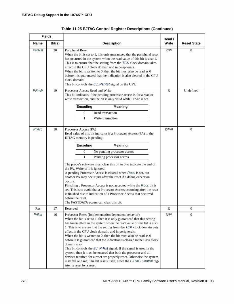
EJTAG Debug Support in the 1074K™ CPU
278 MIPS32® 1074K™ CPU Family Software User’s Manual, Revision 01.03
PerRst 20 Peripheral ResetWhen the bit is set to 1, it is only guaranteed that the peripheral resethas occurred in the system when the read value of this bit is also 1.This is to ensure that the setting from the TCK clock domain takeseffect in the CPU clock domain and in peripherals.When the bit is written to 0, then the bit must also be read as 0before it is guaranteed that the indication is also cleared in the CPUclock domain.This bit controls the EJ_PerRst signal on the CPU.
R/W 0
PRnW 19 Processor Access Read and WriteThis bit indicates if the pending processor access is for a read orwrite transaction, and the bit is only valid while PrAcc is set.
R Undefined
PrAcc 18 Processor Access (PA)Read value of this bit indicates if a Processor Access (PA) to theEJTAG memory is pending:
The probe’s software must clear this bit to 0 to indicate the end ofthe PA. Write of 1 is ignored.A pending Processor Access is cleared when Rocc is set, butanother PA may occur just after the reset if a debug exceptionoccurs.Finishing a Processor Access is not accepted while the Rocc bit isset. This is to avoid that a Processor Access occurring after the resetis finished due to indication of a Processor Access that occurredbefore the reset.The FASTDATA access can clear this bit.
R/W0 0
Res 17 Reserved R 0
PrRst 16 Processor Reset (Implementation dependent behavior)When the bit is set to 1, then it is only guaranteed that this settinghas taken effect in the system when the read value of this bit is also1. This is to ensure that the setting from the TCK clock domain getseffect in the CPU clock domain, and in peripherals.When the bit is written to 0, then the bit must also be read as 0before it is guaranteed that the indication is cleared in the CPU clockdomain also.This bit controls the EJ_PrRst signal. If the signal is used in thesystem, then it must be ensured that both the processor and alldevices required for a reset are properly reset. Otherwise the systemmay fail or hang. The bit resets itself, since the EJTAG Control reg-ister is reset by a reset.
R/W 0
Table 11.25 EJTAG Control Register Descriptions (Continued)
Fields
DescriptionRead /Write Reset StateName Bit(s)
Encoding Meaning
0 Read transaction
1 Write transaction
Encoding Meaning
0 No pending processor access
1 Pending processor access

11.4 EJTAG TAP Registers
MIPS32® 1074K™ CPU Family Software User’s Manual, Revision 01.03 279
ProbEn 15 Probe EnableThis bit indicates to the CPU if the EJTAG memory is handled bythe probe so processor accesses are answered:
It is an error by the software controlling the probe if it sets the Prob-Trap bit to 1, but resets the ProbEn to 0. The operation of the pro-cessor is UNDEFINED in this case.The ProbEn bit is reflected as a read-only bit in the ProbEn bit, bit0, in the Debug Control Register (DCR).The read value indicates the effective value in the DCR, due to syn-chronization issues between TCK and CPU clock domains; however,it is ensured that change of the ProbEn prior to setting the EjtagBrkbit will have effect for the debug handler executed due to the debugexception.The reset value of the bit depends on whether the EJTAGBOOTindication is given or not:
R/W 0 or 1from
EJTAGBOOT
Table 11.25 EJTAG Control Register Descriptions (Continued)
Fields
DescriptionRead /Write Reset StateName Bit(s)
Encoding Meaning
0 The probe does not handle EJTAGmemory transactions
1 The probe does handle EJTAG mem-ory transactions
Encoding Meaning
0 Processor is in non-debug mode (NoEJTAGBOOT indication given)
1 Processor is in debug mode (EJTAG-BOOT indication given)
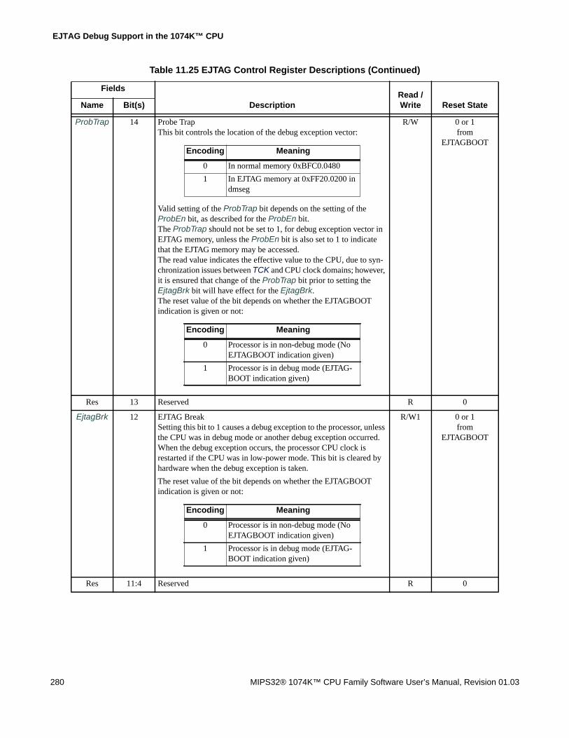
EJTAG Debug Support in the 1074K™ CPU
280 MIPS32® 1074K™ CPU Family Software User’s Manual, Revision 01.03
ProbTrap 14 Probe TrapThis bit controls the location of the debug exception vector:
Valid setting of the ProbTrap bit depends on the setting of theProbEn bit, as described for the ProbEn bit.The ProbTrap should not be set to 1, for debug exception vector inEJTAG memory, unless the ProbEn bit is also set to 1 to indicatethat the EJTAG memory may be accessed.The read value indicates the effective value to the CPU, due to syn-chronization issues between TCK and CPU clock domains; however,it is ensured that change of the ProbTrap bit prior to setting theEjtagBrk bit will have effect for the EjtagBrk.The reset value of the bit depends on whether the EJTAGBOOTindication is given or not:
R/W 0 or 1from
EJTAGBOOT
Res 13 Reserved R 0
EjtagBrk 12 EJTAG BreakSetting this bit to 1 causes a debug exception to the processor, unlessthe CPU was in debug mode or another debug exception occurred.When the debug exception occurs, the processor CPU clock isrestarted if the CPU was in low-power mode. This bit is cleared byhardware when the debug exception is taken.
The reset value of the bit depends on whether the EJTAGBOOTindication is given or not:
R/W1 0 or 1from
EJTAGBOOT
Res 11:4 Reserved R 0
Table 11.25 EJTAG Control Register Descriptions (Continued)
Fields
DescriptionRead /Write Reset StateName Bit(s)
Encoding Meaning
0 In normal memory 0xBFC0.0480
1 In EJTAG memory at 0xFF20.0200 indmseg
Encoding Meaning
0 Processor is in non-debug mode (NoEJTAGBOOT indication given)
1 Processor is in debug mode (EJTAG-BOOT indication given)
Encoding Meaning
0 Processor is in non-debug mode (NoEJTAGBOOT indication given)
1 Processor is in debug mode (EJTAG-BOOT indication given)

11.4 EJTAG TAP Registers
MIPS32® 1074K™ CPU Family Software User’s Manual, Revision 01.03 281
11.4.3 Processor Access Address Register
The Processor Access Address (PAA) register is used to provide the address of the processor access in the dmseg, andthe register is only valid when a processor access is pending. The length of the Address register is 32 bits, and thisregister is selected by shifting in the ADDRESS instruction.
11.4.3.1 Processor Access Data Register
The Processor Access Data (PAD) register is used to provide data value to and from a processor access. The length ofthe Data register is 32 bits, and this register is selected by shifting in the DATA instruction.
The register has the written value for a processor access write due to a CPU store to the dmseg, and the output fromthis register is only valid when a processor access write is pending. The register is used to provide the data value for aprocessor access read due to a CPU load or fetch from the dmseg, and the register should only be updated with a newvalue when a processor access write is pending.
The PAD register is 32 bits wide. Data alignment is not used for this register, so the value in the PAD register matchesdata on the internal bus. The undefined bytes for a PA write are undefined, and for a PAD read then 0 (zero) must beshifted in for the unused bytes.
The organization of bytes in the PAD register depends on the endianess of the CPU, as shown in Figure 11.20. Theendian mode for debug/kernel mode is determined by the state of the SI_Endian input at power-up.
DM 3 Debug ModeThis bit indicates the debug or non-debug mode:
The bit is sampled in the Capture-DR state of the TAP controller.
R 0
Res 2:0 Reserved R 0
Table 11.25 EJTAG Control Register Descriptions (Continued)
Fields
DescriptionRead /Write Reset StateName Bit(s)
Encoding Meaning
0 Processor is in non-debug mode
1 Processor is in debug mode

EJTAG Debug Support in the 1074K™ CPU
282 MIPS32® 1074K™ CPU Family Software User’s Manual, Revision 01.03
Figure 11.20 Endian Formats for PAD Register
The size of the transaction and thus the number of bytes available/required for the PAD register is determined by thePsz field in the ECR.
11.4.4 Fastdata Register (TAP Instruction FASTDATA)
The width of the Fastdata register is 1 bit. During a Fastdata access, the Fastdata register is written and read, i.e., a bitis shifted in and a bit is shifted out. During a Fastdata access, the Fastdata register value shifted in specifies whetherthe Fastdata access should be completed or not. The value shifted out is a flag that indicates whether the Fastdataaccess was successful or not (if completion was requested).
Figure 11.21 Fastdata Register Format
The FASTDATA access is used for efficient block transfers between dmseg (on the probe) and target memory (on theprocessor). An “upload” is defined as a sequence of processor loads from target memory and stores to dmseg. A“download” is a sequence of processor loads from dmseg and stores to target memory. The “Fastdata area” specifiesthe legal range of dmseg addresses (0xFF20.0000 - 0xFF20.000F) that can be used for uploads and downloads. The
0
SPrAcc
Table 11.26 Fastdata Register Field Description
Fields
DescriptionRead /Write
Power-upStateName Bits
SPrAcc 0 Shifting in a zero value requests completion of the Fastdata access.The PrAcc bit in the EJTAG Control register is overwritten withzero when the access succeeds. (The access succeeds if PrAcc isone, and the operation address is in the legal dmseg Fastdata area.)When successful, a one is shifted out. Shifting out a zero indicatesa Fastdata access failure.Shifting in a one does not complete the Fastdata access, and thePrAcc bit is unchanged. Shifting out a one indicates that the accesswould have been successful if allowed to complete, and a zeroindicates the access would not have successfully completed.
R/W Undefined
A[n:0]=7 6 5 4
012A[n:0]=3
A[n:0]=4 5 6 7
321A[n:0]=0
0781516232431
0781516232431
LSBbit
MSB
LSBbit
MSB
A[n:2]=1
A[n:2]=0
A[n:2]=1
A[n:2]=0
Most-significant byte is at lowest address.Word is addressed by byte address of most-significant byte.
BIG-ENDIAN
LITTLE-ENDIAN
Least-significant byte is at lowest address.Word is addressed by byte address of least-significant byte.

11.5 TAP Processor Accesses
MIPS32® 1074K™ CPU Family Software User’s Manual, Revision 01.03 283
Data plus Fastdata registers (selected with the FASTDATA instruction) allow efficient completion of pending Fast-data area accesses.
During Fastdata uploads and downloads, the processor will stall on accesses to the Fastdata area. The PrAcc (proces-sor access pending bit) will be 1, indicating the probe is required to complete the access. Both upload and downloadaccesses are attempted by shifting in a zero SPrAcc value (to request access completion) and shifting out SPrAcc tosee if the attempt will be successful (i.e., there was an access pending and a legal Fastdata area address was used).Downloads will also shift in the data to be used to satisfy the load from dmseg’s Fastdata area, while uploads willshift out the data being stored to dmseg’s Fastdata area.
As noted above, two conditions must be true for the Fastdata access to succeed:
• PrAcc must be 1, i.e., there must be a pending processor access.
• The Fastdata operation must use a valid Fastdata area address in dmseg (0xFF20.0000 to 0xFF20.000F).
Table 11.27 shows the values of the PrAcc and SPrAcc bits and the results of a Fastdata access.
There are no restrictions on the contents of the Data register. It is expected that the transfer size is negotiated betweenthe download/upload transfer code and the probe software. Note that the most efficient transfer size is a 32-bit word.
The Rocc bit of the ECR register is not used for the FASTDATA operation.
11.5 TAP Processor Accesses
The TAP modules support handling of fetches, loads and stores from the CPU through the dmseg segment, wherebythe TAP module can operate like a slave unit connected to the on-chip bus. The CPU can then execute code takenfrom the EJTAG Probe and it can access data (via a load or store) which is located on the EJTAG Probe. This occursin a serial way through the EJTAG interface: the CPU can thus execute instructions e.g. debug monitor code, withoutoccupying the memory.
Table 11.27 Operation of the FASTDATA Access
ProbeOperation
AddressMatchCheck
PrAcc inthe Control
Register
LSB(SPrAcc)Shifted In
Action inthe DataRegister
PrAccChanges to
LSBShiftedOut
DataShifted Out
Downloadusing FAST-DATA
Fails x x none unchanged 0 invalid
Passes 1 1 none unchanged 1 invalid
1 0 write data 0 (SPrAcc) 1 valid (previ-ous) data
0 x none unchanged 0 invalid
Upload usingFASTDATA
Fails x x none unchanged 0 invalid
Passes 1 1 none unchanged 1 invalid
1 0 read data 0 (SPrAcc) 1 valid data
0 x none unchanged 0 invalid
EJTAG Debug Support in the 1074K™ CPU
284 MIPS32® 1074K™ CPU Family Software User’s Manual, Revision 01.03
Accessing the dmseg segment (EJTAG memory) can only occur when the processor accesses an address in the rangefrom 0xFF20.0000 to 0xFF2F.FFFF, the ProbEn bit is set, and the processor is in debug mode (DM=1). In additionthe LSNM bit in the CP0 Debug register controls transactions to/from the dmseg.
When a debug exception is taken, while the ProbTrap bit is set, the processor will start fetching instructions fromaddress 0xFF20.0200.
A pending processor access can only finish if the probe writes 0 to PrAcc or by a reset.
11.5.1 Fetch/Load and Store From/To the EJTAG Probe Through dmseg
1. The internal hardware latches the requested address into the PA Address register (in case of the Debug exception:0xFF20.0200).
2. The internal hardware sets the following bits in the EJTAG Control register:PrAcc = 1 (selects Processor Access operation)PRnW = 0 (selects processor read operation)Psz[1:0] = value depending on the transfer size
3. The EJTAG Probe selects the EJTAG Control register, shifts out this control register’s data and tests the PrAcc sta-tus bit (Processor Access): when the PrAcc bit is 1, the requested address is available and can be shifted out.
4. The EJTAG Probe checks the PRnW bit to determine the required access.
5. The EJTAG Probe selects the PA Address register and shifts out the requested address.
6. The EJTAG Probe selects the PA Data register and shifts in the instruction corresponding to this address.
7. The EJTAG Probe selects the EJTAG Control register and shifts a PrAcc = 0 bit into this register to indicate to theprocessor that the instruction is available.
8. The instruction becomes available in the instruction register and the processor starts executing.
9. The processor increments the program counter and outputs an instruction read request for the next instruction.This starts the whole sequence again.
Using the same protocol, the processor can also execute a load instruction to access the EJTAG Probe’s memory. Forthis to happen, the processor must execute a load instruction (e.g. a LW, LH, LB) with the target address in the appro-priate range.
Almost the same protocol is used to execute a store instruction to the EJTAG Probe’s memory through dmseg. Thestore address must be in the range: 0xFF20.0000 to 0xFF2F.FFFF, the ProbEn bit must be set and the processor has tobe in debug mode (DM=1). The sequence of actions is found below:
1. The internal hardware latches the requested address into the PA Address register.
2. The internal hardware latches the data to be written into the PA Data register.
3. The internal hardware sets the following bits in the EJTAG Control register:PrAcc = 1 (selects Processor Access operation)PRnW = 1 (selects processor write operation)Psz[1:0] = value depending on the transfer size

11.6 PC Sampling
MIPS32® 1074K™ CPU Family Software User’s Manual, Revision 01.03 285
4. The EJTAG Probe selects the EJTAG Control register, shifts out this control register’s data and tests the PrAcc sta-tus bit (Processor Access): when the PrAcc bit is found 1, it means that the requested address is available and canbe shifted out.
5. The EJTAG Probe checks the PRnW bit to determine the required access.
6. The EJTAG Probe selects the PA Address register and shifts out the requested address.
7. The EJTAG Probe selects the PA Data register and shifts out the data to be written.
8. The EJTAG Probe selects the EJTAG Control register and shifts a PrAcc = 0 bit into this register to indicate to theprocessor that the write access is finished.
9. The EJTAG Probe writes the data to the requested address in its memory.
10. The processor detects that PrAcc bit = 0, which means that it is ready to handle a new access.
The above examples imply that no reset occurs during the operations, and that Rocc is cleared.
11.6 PC Sampling
The PC sampling feature enables periodic sampling of the PC value. This information can be used for statistical pro-filing akin to gprof and is also very useful for detecting hot-spots in the code. PC sampling cannot be turned on oroff, that is, the PC value is continually sampled.
The presence or absence of the PC Sampling feature is specified in Debug ControlPCS (bit 9). The sampled PC valuesare written into a TAP register. The old value in the TAP register is overwritten by a new value, even if this registerhas not been read out by the debug probe. The sample rate is specified in a manner similar to the PDtrace synchroni-zation period, with three bits. These bits in the Debug Control register are 8:6 and called PCSR (PC SampleRate).
These three bits take the value 25 to 212 similar to SyncPeriod. Note that the processor samples PC even when it isasleep (in a WAIT state). This permits an analysis of the amount of time spent by a processor in WAIT state whichmay be used for example to revert to a low-power mode during the non-execution phase of a real-time application.
The sampled values includes a New data bit, the PC, the ASID of the sampled PC, and the Thread Context ID if theprocessor implements the MIPS MT ASE. Figure 11.22 shows the format of the sampled values in the TAP registerPCsample. The new data bit is used by the probe to determine if the PCsample register data just read out is new oralready been read and must be discarded.
Figure 11.22 TAP Register PCsample Format
The sampled PC value is the PC of the graduating instruction in the current cycle. If the processor is stalled when thePC sample counter overflows, then the sampled PC is the PC of the next graduating instruction. The processor contin-ues to sample the PC value even when it is in Debug mode.
48 41 40 33 32 1 0
TC (for MIPS MTprocessors only)
ASID PC New

EJTAG Debug Support in the 1074K™ CPU
286 MIPS32® 1074K™ CPU Family Software User’s Manual, Revision 01.03
11.6.1 PC Sampling in Wait State
When the processor is in a WAIT state (to save power, for example), an external agent might want to know how longit stays in the WAIT state. But counting cycles to update the PC sample value is a waste of power. Hence, when in aWAIT state, the processor must simply switch the New bit to 1 every time it is set to 0 by the probe hardware. Hence,the external agent or probe reading the PC value will detect a WAIT instruction for as long as the processor remains inthe WAIT state. When the processor leaves the WAIT state, counting is resumed as before.
11.7 Fast Debug Channel
The Fast Debug Channel (FDC) mechanism provides an efficient means to transfer data between the CPU and anexternal device using the EJTAG TAP pins. The external device would typically be an EJTAG probe and that is theterm used here, but it could be something else. FDC utilizes two First In First Out (FIFO) structures to buffer databetween theCPU and probe. The probe uses the FDC TAP instruction to access these FIFOs, while the CPU itselfaccesses them using memory accesses. To transfer data out of the CPU, the CPU writes one or more pieces of data tothe transmit FIFO. At this time, the CPU can resume doing other work. An external probe would examine the statusof the transmit FIFO periodically. If there is data to be read, the probe starts to receive data from the FIFO, one entryat a time. When all data from the FIFO has been drained, the probe goes back to waiting for more data. The CPU caneither choose to be informed of the empty transmit FIFO via an interrupt, or it can choose to periodically check thestatus. Receiving data works in a similar manner - the probe writes to the receive FIFO. At that time, the CPU is eitherinterrupted, or finds out via polling a status bit. The CPU can then do load accesses to the receive FIFO and receivedata being sent to it by the probe. The TAP transfer is bidirectional - a single shift can be pulling transmit data andputting receive data at the same time.
The primary advantage of FDC over normal processor accesses or fastdata accesses is that it does not require the CPUto be blocked when the probe is reading or writing to the data transfer FIFOs. This significantly reduces the CPUoverhead and makes the data transfer far less intrusive to the code executing on the CPU.
Refer to the EJTAG Specification [12] for the general details on FDC. The remainder of this section describes imple-mentation specific behavior and register values.
The FDC memory mapped registers are located in the common device memory map (CDMM) region. FDC has adevice ID of 0xFD.
11.7.1 Common Device Memory Map
Software on the CPU accesses FDC through memory mapped registers. These memory mapped registers are locatedwithin the Common Device Memory Map (CDMM). The CDMM is a region of physical address space that isreserved for mapping IO device configuration registers within a MIPS processor. The base address and enabling ofthis region is controlled by the CDMMBase CP0 register, see Section 7.2.22 “CDMMBase Register (CP0 Register15, Select 2)”.
Refer to Volume III of the Architecture Reference Manuals [15] for full details on CDMM.
11.7.2 Fast Debug Channel Interrupt
The FDC block can generate an interrupt to inform software of incoming data being available or space being availablein the outgoing FIFO. This interrupt is handled similarly to the timer or performance counter interrupts. TheCauseFDCI bit indicates that the interrupt is pending. The interrupt is also sent to the CPU output SI_FDCI where it iscombined with one of the SI_Int pins. For non-EIC mode, the SI_IPFDCI input indicates which interrupt pin is has

11.7 Fast Debug Channel
MIPS32® 1074K™ CPU Family Software User’s Manual, Revision 01.03 287
been combined with and this information is reflected in the IntCtlIPFDCI field. Note that this interrupt is a regular inter-rupt and not a debug interrupt.
The FDC Configuration Register (see Section 11.7.6.2 “FDC Configuration (FDCFG) Register (Offset 0x8)”)includes fields for enabling and setting the threshold for generating each interrupt. Receive and transmit interruptthresholds are specified independently, but they are ORed together to form a single interrupt .
The following interrupt thresholds are supported:
• Interrupts Disabled: No interrupt will be generated and software must poll the status registers to determine ifincoming data is available or if there is space for outgoing data.
• Minimum CPU Overhead: This setting minimizes the CPU overhead by not generating an interrupt until thereceive FIFO (RxFIFO) is completely full or the transmit FIFO (TxFIFO) is completely empty.
• Minimum latency: To have the CPU take data as soon as it is available, the receive interrupt can be fired when-ever the RxFIFO is not empty. There is a complimentary TxFIFO not full setting although that may not be quiteas useful.
• Maximum bandwidth: When configured for minimum CPU overhead, bandwidth between the probe and CPUcan be wasted if the CPU does not service the interrupt before the next transfer occurs. To reduce the chances ofthis happening, the interrupt threshold can be set to almost full or almost empty to generate an interrupt earlier.This setting causes receive interrupts to be generated when there are 0 or 1 unused RxFIFO entries. Transmitinterrupts are generated when there are 0 or 1 used TxFIFO entries (see note in following section about this con-dition)
11.7.3 1074K™CPU FDC Buffers
Figure 11.23 shows the general organization of the transmit and receive buffers on the 1074K CPU.

EJTAG Debug Support in the 1074K™ CPU
288 MIPS32® 1074K™ CPU Family Software User’s Manual, Revision 01.03
Figure 11.23 Fast Debug Channel Buffer Organization
One particular thing to note is the asynchronous crossings between the EJ_TCK and SI_ClkIn clock domains. Thiscrossing is handled with a handshake interface that safely transfers data between the domains. Two data registers areincluded in this interface, one in the source domain and one in the destination domain. The control logic activelymanages these registers so that they can be used as FIFO entries. The fact that one FIFO entry is in the EJ_TCK clockdomain is normally transparent, but it can create some unexpected behavior:
• TxFIFO availability: Data is first written into the SI_Clk FIFO entries, then it will move into the EJ_TCK FIFOentry. But, it takes several EJ_TCK cycles to complete the handshake and move the data. EJ_TCK is generallymuch slower than SI_ClkIn and may even be stopped (although that would be uncommon when this feature is inuse). This can result in there not being space for new data, even though there are only N-1 data values queued up.To prevent the loss of data, the FDSTATTxF bit is set when all of the SI_ClkIn FIFO entries are full. Software writ-ing to the FIFO should always check the FDSTATTxF bit prior to attempting a write and should not make anyassumptions about being able to arbitrarily use all entries. i.e., software seeing the FDSTATFxE bit set should notassume that it can write FDCFGTxCnt data words without checking for full.
• TxFIFO Almost Empty Interrupt: As transmit data moves from SI_ClkIn to EJ_TCK, both of the flops will tem-porarily look full. This makes it difficult to determine when just 1 FIFO entry is in use. To enable a simpler con-dition, the almost empty TxInterrupt condition is set when all of the SI_ClkIn FIFO entries are empty. When this
Chan Data
AddrDecode
Store Data to FDTXnStore Address Load from FDSTAT Load from FDRX
SI_ClkIn
EJ_TCK
Chan DataStatus
Capture-DR Update-DR
EJ_TDOEJ_TDI
ControlLogic
TxFIFO RxFIFO
Shift Register
Chan Data
Chan Data Chan Data
Chan Data
Chan Data

11.7 Fast Debug Channel
MIPS32® 1074K™ CPU Family Software User’s Manual, Revision 01.03 289
condition is met, there will be 0 or 1 valid entries. However, the interrupt will not be asserted when there is onlyone valid entry if it is an SI_ClkIn entry
• The RxFIFO has similar characteristics but these are even less visible to software since SI_ClkIn must be runningto access the FDC registers.
11.7.4 Sleep mode
FDC data transfers do not prevent the CPU from entering sleep mode and will proceed normally in sleep mode. TheFDC block monitors the TAP interface signals with a free-running clock. When new receive data is available or trans-mit data can be sent, the gated clock will be enabled for a few cycles to transfer the data and then allowed to stopagain. If FDC interrupts are enabled, transferring data may cause an interrupt to be generated which can wake theCPU up.
11.7.5 FDC TAP Register
The FDC TAP instruction performs a 38 bit bidirectional transfer of the FDC TAP register. The register format isshown in Figure 11.24 and the fields are described in Figure 11.28
Figure 11.24 FDC TAP Register Format
37 36 35 32 31 0
InProbe Data
AcceptData InValid
ChannelID Data
OutReceive
Buffer FullData Out
Valid
Table 11.28 FDC TAP Register Field Descriptions
Fields
DescriptionRead /Write
ResetStateName Bits
Probe DataAccept
37 Indicates to CPU that the probe is accepting the data thatwas scanned out.
W Undefined
Data In Valid 36 Indicates to CPU that the probe is sending new data to thereceive FIFO.
W Undefined
ReceiveBuffer Full
37 Indicates to probe that the receive buffer is full and theCPU will not accept the data being scanned in. Analogousto ProbeDataAccept, but opposite polarity
R 0x0
Data OutValid
36 Indicates to probe that the CPU is sending new data fromthe transmit FIFO
R 0
ChannelID 35:32 Channel number associated with the data being scanned inor out. This field can be used to indicate the type of datathat is being sent and allow independent communicationchannels
Scanning in a value with ChannelID=0xd and Data InValid = 0 will generate a receive interrupt. This can beused when the probe has completed sending data to theCPU.
R/W Undefined

EJTAG Debug Support in the 1074K™ CPU
290 MIPS32® 1074K™ CPU Family Software User’s Manual, Revision 01.03
11.7.6 Fast Debug Channel Registers
This section describes the Fast Debug Channel registers. CPU access to FDC is via loads and stores to the FDCdevice in the Common Device Memory Map (CDMM) region. These registers provide access control, configurationand status information, as well as access to the transmit and receive FIFOs. The registers and their respective offsetsare shown in Table 11.29
11.7.6.1 FDC Access Control and Status (FDACSR) Register (Offset 0x0)
This is the general CDMM Access Control and Status register which defines the device type and size and controlsuser and supervisor access to the remaining FDC registers. The Access Control and Status register itself is only acces-sible in kernel mode. Figure 11.25 has the format of an Access Control and Status register (shown as a 64-bit regis-ter), and Table 11.30 describes the register fields.
Figure 11.25 FDC Access Control and Status Register Format
Data 31:0 Data value being scanned in or out R/W Undefined
Table 11.29 FDC Register Mapping
Offset in CDMMDevice Block
RegisterMnemonic Register Name and Description
0x0 FDACSR FDC Access Control and Status Register
0x8 FDCFG FDC Configuration Register
0x10 FDSTAT FDC Status Register
0x18 FDRX FDC Receive Register
0x20 + 0x8* n FDTXn FDC Transmit Register n (0 ≤ n ≤ 15)
63 32 31 24 23 22 21 16 15 12 11 4 3 2 1 0
0 DevID 0 DevSize DevRev 0 Uw Ur Sw Sr
Table 11.30 FDC Access Control and Status Register Field Descriptions
Fields
DescriptionRead /Write
ResetStateName Bits
DevID 31:24 This field specifies the type of device. R 0xfd
DevSize 21:16 This field specifies the number of extra 64-byte blocksallocated to this device. The value 0x2 indicates that thisdevice uses 2 extra, or 3 total blocks.
R 0x2
DevRev 15:12 This field specifies the revision number of the device. Thevalue 0x0 indicates that this is the initial version of FDC.
R 0x0
Table 11.28 FDC TAP Register Field Descriptions
Fields
DescriptionRead /Write
ResetStateName Bits

11.7 Fast Debug Channel
MIPS32® 1074K™ CPU Family Software User’s Manual, Revision 01.03 291
11.7.6.2 FDC Configuration (FDCFG) Register (Offset 0x8)
The FDC configuration register holds information about the current configuration of the Fast Debug Channel mecha-nism. Figure 11.26 has the format of the FDC Configuration register, and Table 11.31 describes the register fields.
Figure 11.26 FDC Configuration Register Format
Uw 3 This bit indicates if user-mode write access to this deviceis enabled. A value of 1 indicates that access is enabled. Avalue of 0 indicates that access is disabled. An attempt towrite to the device while in user mode with access dis-abled is ignored.
R/W 0
Ur 2 This bit indicates if user-mode read access to this device isenabled. A value of 1 indicates that access is enabled. Avalue of 0 indicates that access is disabled. An attempt toread from the device while in user mode with access dis-abled will return 0 and not change any state.
R/W 0
Sw 1 This bit indicates if supervisor-mode write access to thisdevice is enabled. A value of 1 indicates that access isenabled. A value of 0 indicates that access is disabled. Anattempt to write to the device while in supervisor modewith access disabled is ignored.
R/W 0
Sr 0 This bit indicates if supervisor-mode read access to thisdevice is enabled. A value of 1 indicates that access isenabled. A value of 0 indicates that access is disabled. Anattempt to read from the device while in supervisor modewith access disabled will return 0 and not change anystate..
R/W 0
0 11:4 Reserved for future use. Ignored on write; returns zero onread.
R 0
31 20 19 18 17 16 15 8 7 0
0 Tx_IntThresh Rx_IntThresh TxFIFOSize RxFIFOSize
Table 11.31 FDC Configuration Register Field Descriptions
Fields
DescriptionRead /Write
ResetStateName Bits
0 31:20 Reserved for future use. Read as zeros, must be written aszeros.
R 0
Table 11.30 FDC Access Control and Status Register Field Descriptions (Continued)
Fields
DescriptionRead /Write
ResetStateName Bits

EJTAG Debug Support in the 1074K™ CPU
292 MIPS32® 1074K™ CPU Family Software User’s Manual, Revision 01.03
11.7.6.3 FDC Status (FDSTAT) Register (Offset 0x10)
The FDC Status register holds up to date state information for the FDC mechanism. Figure 11.27 has the format ofthe FDC Status register, and Table 11.32 describes the register fields.
Figure 11.27 FDC Status Register Format
TxIntThresh 19:18 Controls whether transmit interrupts are enabled and thestate of the TxFIFO needed to generate an interrupt.
R/W 0
RxIntThresh 17:16 Controls whether receive interrupts are enabled and thestate of the RxFIFO needed to generate an interrupt.
R/W 0
TxFIFOSize 15:8 This field holds the total number of entries in the transmitFIFO.
R Preset
RxFIFOSize 7:0 This field holds the total number of entries in the receiveFIFO.
R Preset
31 24 23 16 15 8 7 4 3 2 1 0
Tx_Count Rx_Count 0 RxChan RxE RxF TxE TxF
Table 11.32 FDC Status Register Field Descriptions
Fields
DescriptionRead /Write
ResetStateName Bits
Tx_Count 31:24 This optional field is not implemented and will read as 0 R 0
Rx_Count 23:16 This optional field is not implemented and will read as 0 R 0
Table 11.31 FDC Configuration Register Field Descriptions (Continued)
Fields
DescriptionRead /Write
ResetStateName Bits
Encoding Meaning
0 Transmit Interrupt Disabled
1 Empty
2 Not Full
3 Almost Empty - zero or one entry inuse*(see 11.7.2 for specifics)
Encoding Meaning
0 Receive Interrupt Disabled
1 Full
2 Not empty
3 Almost Full - zero or one entry free

11.7 Fast Debug Channel
MIPS32® 1074K™ CPU Family Software User’s Manual, Revision 01.03 293
11.7.6.4 FDC Receive (FDRX) Register (Offset 0x18)
This register exposes the top entry in the receive FIFO. A read from this register returns the top item in the FIFO andremoves it from the FIFO itself. The result of a write to this register is UNDEFINED. The result of a read when theFIFO is empty is also UNDEFINED so software must check the FDSTATRxE flag prior to reading. Figure 11.28 hasthe format of the FDC Receive register, and Table 11.33 describes the register fields.
Figure 11.28 FDC Receive Register Format
11.7.6.5 FDC Transmit n (FDTXn) Registers (Offset 0x20 + 0x8*n)
These sixteen registers all access the bottom entry in the transmit FIFO. The different addresses are used to generate a4b channel identifier that is attached to the data value. This allows software to track different event types withoutneeding to reserve a portion of the 32b data as a tag. A write to one of these registers results in a write to the transmitFIFO of the data value and channel ID corresponding to the register being written. Reads from these registers areUNDEFINED. Attempting to write to the transmit FIFO if it is full has UNDEFINED results. Hence, the softwarerunning on the CPU must check the FDSTATTxF flag to ensure that there is space for the write. Figure 11.29 has theformat of the FDC Transmit register, and Table 11.34 describes the register fields.
Figure 11.29 FDC Transmit Register Format
0 15:8 Reserved for future use. Must be written as zeros and readas zeros.
R 0
RxChan 7:4 This field indicates the channel number used by the topitem in the receive FIFO. This field is only valid if RxE=0.
R Undefined
RxE 3 If RxE is set, the receive FIFO is empty. If RxE is not set,the FIFO is not empty.
R 1
RxF 2 If RxF is set, the receive FIFO is full. If RxF is not set, theFIFO is not full.
R 0
TxE 1 If TxE is set, the transmit FIFO is empty. If TxE is not set,the FIFO is not empty.
R 1
TxF 0 If TxF is set, the transmit FIFO is full. If TxF is not set, theFIFO is not full.
R 0
31 0
RxData
Table 11.33 FDC Receive Register Field Descriptions
Fields
DescriptionRead /Write
ResetStateName Bits
RxData 31:0 This register holds the top entry in the receive FIFO R Undefined
31 0
TxData
Table 11.32 FDC Status Register Field Descriptions (Continued)
Fields
DescriptionRead /Write
ResetStateName Bits

EJTAG Debug Support in the 1074K™ CPU
294 MIPS32® 1074K™ CPU Family Software User’s Manual, Revision 01.03
11.8 MIPS® Trace
The optional MIPS Trace block provides the user with an informative method of tracing program flow, load/storeaddresses and data, performance counters, and CPU-specific inefficiencies. The level of information which is traced,for example, tracing only when in specific processor modes (e.g., User Mode or Kernel Mode) is controlled byrun-time options.
When MIPS Trace is implemented, the CP0 Config3TL bit is set by hardware when the CPU is configured.
The pipeline-specific architecture of MIPS Trace is specified in the PDtrace™ Interface and Trace Control BlockSpecification [13].
There are two primary functional blocks: the PDtrace capture block and the blocks that implement the functionality ofthe Trace Control Block (TCB). The PDtrace capture block extracts the trace information from the end of the proces-sor pipeline from the in-order graduation stage and stores the information in an internal FIFO called the UnifiedFIFO. The capture block then presents the data from the Unified FIFO to the PDtrace compression block.
The functionality of the TCB is specified in
The compression block and the TCB Registers implement the Trace Control Block (TCB). Though there is not anexplicit module called TCB, the functionality of the TCB, as specified in [13], has been completely implemented andintegrated into the PDtrace unit. Thus, it is no longer a customer option to implement a custom TCB.
Note that the generic pin interface, as defined in the retired document PDtrace™ Interface Specification, that wasused to “communicate” between the capture and the TCB functionality is deprecated. The interface is replaced by aninternal interface that is called the capture-to-compression interface. This interface is embedded inside the 1074KCPU, and will not be discussed in detail here. Suffice it to say that the internal interface embodies all the functionalitydescribed in [13]. While working closely together, the two parts of MIPS Trace are controlled separately by software.Figure 11.30 shows an overview of the MIPS Trace modules within the CPU.
Table 11.34 FDC Transmit Register Field Descriptions
Fields
DescriptionRead /Write
ResetStateName Bits
TxData 31:0 This register holds the bottom entry in the transmit FIFO W,Undefinedvalue on
read
Undefined
Table 11.35 FDTXn Address Decode
Addr Chan Addr Chan Addr Chan Addr Chan
0x20 0x0 0x40 0x4 0x60 0x8 0x80 0xc
0x28 0x1 0x48 0x5 0x68 0x9 0x88 0xd
0x30 0x2 0x50 0x6 0x70 0xa 0x90 0xe
0x38 0x3 0x58 0x7 0x78 0xb 0x98 0xf


EJTAG Debug Support in the 1074K™ CPU
296 MIPS32® 1074K™ CPU Family Software User’s Manual, Revision 01.03
• Only instructions which complete at the end of the pipeline are traced, and indicated with a completion-flag.The PC is implicitly pointing to the next instruction.
• Load instructions are indicated with a load-flag.
• Store instructions are indicated with a store-flag1.
• Taken branches are indicated with a branch-taken-flag on the target instruction.
• New PC information for a branch is only traced if the branch target is unpredictable from the static programimage.
• When branch targets are unpredictable, only the delta value from the current PC is traced, if it is dynamicallydetermined to reduce the number of bits necessary to indicate the new PC. Otherwise the full PC value istraced.
• When a completing instruction is executed in a different processor mode from the previous one, the new pro-cessor mode is traced.
• The first instruction is always traced as a branch target, with processor mode and full PC.
• Periodic synchronization instructions are identified with a sync-flag, and traced with the processor mode andfull PC. The sync instruction is not a load and not a store.
All the instruction flags above are combined into one, 3-bit value, called the “instruction completion” to minimize thebit information to trace. The possible processor modes are explained in Section 11.8.1 “Processor Modes”.
The target address is statically predictable for all branch and all jump-immediate instructions. If the branch is taken,then the branch-taken-flag will indicate this. All jump-register instructions and ERET/DERET are instructions whichhave an unpredictable target address. These will have full/delta PC values included in the trace information. Alsotreated as unpredictable are PC changes which occur due to exceptions, such as an interrupt, reset, etc.
Trace regeneration software must know the static program image in memory, in order to reproduce the dynamic flowwith the above information. But this is usually not a problem. Only the virtual value of the PC is used. Physical mem-ory location will typically differ.
It is possible to turn on PC delta/full information for all branches, but this should not normally be necessary. As asafety check for trace regeneration software, a periodic synchronization with a full PC is sent. The period of this syn-chronization is cycle-based and programmable.
11.8.4 Load/Store Address and Data Trace Information
In addition to PC flow, it is possible to get information on the load/store addresses, as well as the data read/written.When enabled, the following information is optionally added to the trace:
• When load-address tracing is on, the full load address of the first load instruction is traced (indicated by theload-flag). For subsequent loads, a dynamically-determined delta to the previous load address is traced tocompress the information which must be sent.
1. An SC (Store Conditional) instruction is flagged as a store instruction, even if the load-locked bit prevented the actual store.Thus the SC does not have special handling and is treated as any other store; it is up to the reconstruction software to deter-mine if the SC succeeded or failed.

11.8 MIPS® Trace
MIPS32® 1074K™ CPU Family Software User’s Manual, Revision 01.03 297
• When store-address tracing is on, the full store address of the first store instruction is traced (indicated by thestore-flag). For subsequent stores, a dynamically-determined delta to the previous store address is traced.
• When load-data tracing is on, the full load data read by each load instruction is traced (indicated by theload-flag). Only actual read bytes are traced.
• When store-data tracing is on, the full store data written by each store instruction is traced (indicated by thestore-flag). Only written bytes are traced.
After each synchronization instruction, the first load address and the first store address following this are both tracedwith the full address if load/store address tracing is enabled.
11.8.5 Programmable Processor Trace Mode Options
To enable tracing, a global Trace On signal must be set. When trace is on, it is possible to enable tracing in any com-bination of the processor modes described in Section 11.8.1 “Processor Modes”. In addition to this, trace can beturned on globally for all processes, or only for specific processes, by tracing only specific masked values of theASID found in EntryHiASID.
Additionally, an EJTAG Simple Break trigger point can override the processor mode and ASID selection and turnthem all on. Another trigger point can disable this override.
11.8.6 Programmable Trace Information Options
The processor mode changes are always traced:
• On the first instruction
• On any synchronization instruction
• When the mode changes, and either the previous or the current processor mode is selected for trace
The amount of extra information traced is programmable to include:
• PC information only
• PC and cross product of load/store address/data
• If the optional performance counter trace is enabled, when the specific events defined in Section11.8.12 “Performance Counter Tracing” occur, up to four performance counter registers are traced.
If the full internal state of the processor is known prior to trace start, PC and load data are the only informationneeded to recreate all register values on an instruction-by-instruction basis.
11.8.6.1 User Data Trace
Two special CP0 registers, UserTraceData1 and UserTraceData2, can generate a data trace. When either of these reg-isters is written, and the global Trace On is set, the 32-bit data written is put in the trace as special User Data informa-tion. Since writing these registers is performed via an MTC0 operation, only one register is updated in any givencycle. Thus in the same cycle, only one of the UserTraceData registers is traced. However, in back to back cycles, thetracing of the two registers can alternate and is handled correctly.
EJTAG Debug Support in the 1074K™ CPU
298 MIPS32® 1074K™ CPU Family Software User’s Manual, Revision 01.03
Note: The User Data is sent even if the processor is operating in an un-traced processor mode.
11.8.7 Enable Trace to Probe On-chip Memory
When trace is On, based on the options listed in Section 11.8.5 “Programmable Processor Trace Mode Options”, thetrace information is continuously sent to the Trace Compression and TCB Control Block. However, the TCB must beenabled to transmit the trace information to the Trace probe or to on-chip trace memory by setting theTCBCONTROLBEN bit. This bit can be set in three ways:
• Set/clear the TCBCONTROLBEN bit via an EJTAG TAP operation.
• Initialize a TCB trigger to set/clear the TCBCONTROLBEN bit.
• Use the drseg mapping of TCBCONTROLB to clear TCBCONTROLBEN via a load to drseg space. SeeSection 11.8.17 “Memory-mapped Access to On-Chip Trace RAM” for special access rules.
11.8.8 TCB Trigger
The TCB can optionally include 0 to 8 triggers. A TCB trigger can be programmed to fire from any combination of:
• Probe Trigger Input to the TCB
• Chip-level Trigger Input to the TCB
• Processor entry into DebugMode
When a trigger fires, it can be programmed to have any combination of actions:
• Create Probe Trigger Output from TCB
• Create Chip-level Trigger Output from TCB
• Set, clear, or start countdown to clear the TCBCONTROLBEN bit (start/end/about trigger)
• Put an information byte into the trace stream, that is, a TF6 is inserted into the trace stream
11.8.9 Cycle-by-Cycle Information
The PDtrace capture block collects all of the trace information listed in Section 11.8.3 “Trace Information” andSection 11.8.4 “Load/Store Address and Data Trace Information”. The trace is then compressed and aligned to fit in64-bit trace words, with no loss of information. It is possible to exclude/include the exact cycle-by-cycle relationshipbetween each instruction. If excluded, the number of bits required in the trace information from the TCB is reduced,and each trace word will only contain information from completing instructions.
11.8.10 Instruction and Data Cache Miss Tracing
It is possible to embed information about Instruction and/or Data cache misses into the trace information, with somelimitations, as described below.
For the instruction cache miss indicator:

11.8 MIPS® Trace
MIPS32® 1074K™ CPU Family Software User’s Manual, Revision 01.03 299
• The instruction cache miss indicator is based on whether the instruction is pulled from the cache or the fill buffer.On a cache miss, the fetch is restarted when the data comes back from the BIU and the instructions will comefrom the Fill Buffer (FB). The miss flag is only set for the first fetch that hits out of the FB to avoid markingevery fetch from the line a miss. However, two instructions can be fetched per cycle and both will be marked as amiss, though if branching to the middle of a dword, only 1 miss will be seen.
• The IFU can prefetch a speculative path which might not be immediately executed. These speculative fetches arefilled into the cache; subsequently, when the code accesses the same address, it is possible that the instructionwill hit in the cache even if that instruction was being executed for the first time.
For the data cache miss indicator:
• PDtrace instruction capture is done at the end of the GRU (graduation) pipe. However, at this point the cachemiss info is not accurate. Hit indication is accurate, but the miss indication is not. The miss could change to a hitafter it enters the LSU graduation buffer. Thus, this miss indicator is instead sent with the data value.
• For loads, this allows an accurate miss indication as the miss state must be resolved before we have the data.
• For stores, the miss indicator is also sent with the data value. The store data value is captured when the storeinstruction exist the LSU graduation buffer.
• The data cache indication was previously a bit in the TF4 trace record that was included with the load or storedata. This bit still exists, but the CM trace correlation described in Section 11.8.11 “Coherence Manager TraceCorrelation”provides a more accurate indication.
11.8.11 Coherence Manager Trace Correlation
In the 1074K Coherent Processing System, trace information is provided from each of the CPUs as well as the Coher-ence Manager. In order to correlate transactions from the CM with the instruction stream, an identifier is used in boththe CPU and CM traces. A new trace format, TF8, is generated by the 1074K to carry the identifier and miss informa-tion. Furthermore, four new CM trace formats are introduced. These are used only by the CM.
11.8.11.1 T8 - New Trace Format for CM Trace Correlation
For load instructions that are treated as potential cache misses (extra bit value of 1 with corresponding INSCOMP),and for all other LSU operations, a TF8 message can potentially be generated. These instructions share one commonattribute: they pass through a hardware structure in the 1074K pipeline. Any instruction that generates a data bustransaction is required to generate a TF8. To minimize bandwidth usage, instructions that do not generate a bus trans-action (typically cache hits) do not generate any additional trace information. However, to allow reconstruction soft-ware to correlate cache miss indicators in the trace stream with the instruction completion indicators in the tracestream, these instructions must be explicitly accounted for. To simplify this process, LSU operations are divided intothree categories: loads, stores, and “other” operations. Each category has an associated 8-bit counter, which countsthe number of cache hits for that category since the last cache miss. This counter is reset to 0 when a miss occurs, orif the counter saturates.
Details of Trace Format 8 (TF8) are shown in Figure 11.31. COSId represents the coherent synchronization ID. TheBT field indicates whether or not a bus transaction has occurred. If BT is zero, no bus transaction has occurred, andthe TF8 is being used to indicate a counter overflow (the COSId value is undefined in this case). If BT is one, a bustransaction was generated for a cache miss, and the corresponding counter must be reset. The L field is used to indi-cate load instructions. If L is 0, the instruction is not a load, if L is 1, the TF8 corresponds to a load instruction. The Sfield is used to indicate store instructions. If S is 0, the instruction is not a store, if S is 1, the TF8 corresponds to astore instruction. If L and S are zero, the instruction is a non load/store LSU operation. L and S can never be 1 in the

EJTAG Debug Support in the 1074K™ CPU
300 MIPS32® 1074K™ CPU Family Software User’s Manual, Revision 01.03
same TF8. To reduce bandwidth consumption, it is recommended that no TF8 be generated by a CPU when the coher-ent interconnect is not tracing transactions (i.e., if the coherent interconnect tracing is turned off globally, or only forthat particular CPU). In addition, a TF8 should only be generated for an instruction that has an instruction completionmessage traced.
Figure 11.31 TF8 (Trace Format 8)
Each TF8 message corresponds to one of the three LSU instruction categories. The category is explicitly identified bythe values of the L and S fields. If a counter hits its maximum count value, the maximum value is sent out in a TF8,along with appropriate values for the L and S fields to identify which counter has saturated. It is possible for a counterto saturate at the same time as a miss. This can be determined by examining the BT bit - in case of a miss, the BT bitmust be 1.
11.8.11.2 Synchronizing CPU and Coherent Interconnect Trace Message
To synchronize CPU trace messages with those gathered from the coherent interconnect, a new identifier (COSId) isadded in the CPU trace block. The COSId is included in trace messages from the CPU and is sent to the coherentinterconnect for inclusion in trace messages. Each CPU maintains an independent COSId, and trace messages fromthe coherent interconnect always hold the COSId of the originating CPU. The COSId is updated periodically when aload or store miss occurs at the processor. The first CPU trace message using the new COSId corresponds to the firstCM message that will use the new COSId, thus providing reconstruction software an exact point at which the twotraces match. Using this match point, other trace messages from the CPU and CM can be correlated. PDtrace supportsperiodic synchronization messages in the form of PC syncs or TMOAS records (A PC sync is a TMOAS record witha SYNC value of 1). The new COSIds will be updated at most as frequently as the CPU sends out a PC sync/TMOASrecord, with one added restriction - the COSId cannot be updated unless a miss occurs. Thus, the CPU can send outmultiple PC syncs without updating the COSId, if no load/store misses occur during that time.
In case of overflow at the CPU, a new PCsync message must be sent. At the same time, the COSId must be updated(so long as there is a corresponding cache miss). In case of overflow at the CM, a signal must be sent back to all CPUsin the system requesting new COSIds. Figure 11-32 illustrates the use of the COSId.
0
Counter S L BT COSId


EJTAG Debug Support in the 1074K™ CPU
302 MIPS32® 1074K™ CPU Family Software User’s Manual, Revision 01.03
Performance counters are traced out based on four specific events. When an enabled event occurs, up to four perfor-mance counters are traced and a fifth value is traced by the CPU. The fifth value is the cycle count register. Tracingthe cycle count register is unique to the CPU.
Control over which particular performance counter is traced is specified by bit PCTD in each Performance CounterControl register. If set to zero (default setting), tracing is enabled for this performance counter, and if set to one, trac-ing is disabled for this performance counter. The cycle counter is traced out if at least one of the performance countercontrol PCTD bits is set, and at least one of the enabled performance counter tracing events occurs. In the case wheremore than one event occurs in the same cycle, the performance counter values are traced only once for that cycle.
1. Synchronization counter expiration will trigger tracing of the performance counter values. This is controlled byTraceControl3PeCSync and TCBCONTROLEPeCSync.
2. Hardware trace breakpoint will trigger tracing of the performance counter values. This is contingent on severalcontrol bit settings. The TE bit in the breakpoint control register should be set. This allows a trigger signal to besent to the Trace Unit. When set, TraceControl3PeCBP / TCBCONTROLEPeCBP act as the enable for performancecounter tracing. Additionally the generation of a performance counter trigger is controlled by setting active bothTraceIBPCPCT and TraceIBPCIE, and, or setting active hi both TraceDBPCPCT and TraceDBPCIE . Furthermore,the BreakPointControl field for the specific hardware breakpoint in TraceIBPC or TraceDBPC must be encoded as3’b100 or 3’b101 to allow performance counter values into the trace stream.
3. Function call, function return, or the occurrence of an exception will trigger tracing of the performance countervalues. This is controlled by TraceControl3PeCFCR / TCBCONTROLEPeCFCR.
4. An overflow of an active performance counter will trigger tracing of the performance counter values. This is con-trolled by TraceControl3PeCOvf / TCBCONTROLEPeCOvf.
The Performance counter data will always use a TF3 with the PCV bit set to one. If the traced data is not Performancecounter data, and performance counter tracing is enabled, then the PCV bit will be zero.
11.8.13 Filtered Data Trace Mode
This mode is used to support tracing of events in application code on a Linux system. This type of instrumented codetracing is primarily used for performance analysis, although it can also be used for event logging and debug. Filtereddata tracing mode provides a mechanism to do low-overhead event tracing from user application code, since theUserTraceData registers require a kernel call from user mode.
In this mode, data load and store addresses are compared to the hardware data breakpoint address. If the addressesmatch, the data value and address associated with that match are traced out.
This mode works even when data address and/or value tracing is turned on. However, the general usage model iswhen both PC and Data trace are turned off since it may not always be possible to identify data that was traced due toa match vs. the regular data stream. This mode is used to shadow one or more static (fixed-address) variables. Whenthere is a store to the variable, the store value is captured into the trace. Since there are generally two or more datatriggers/watchpoints, the trace will need to uniquely identify the shadowed variable by also tracing out the associatedaddress.
Filtered Data Trace mode is controlled by TraceControl2FDT / TCBCONTROLBFDT.

11.8 MIPS® Trace
MIPS32® 1074K™ CPU Family Software User’s Manual, Revision 01.03 303
11.8.14 PC Tracing Off
PC tracing turned off is simply to disable PC tracing which is controlled by TraceControl2Mode.PC /TCBCONTROLCMode.PC. Turning off this bit has more implications than simply not tracing the PC. There is somespecial behavior which is contingent on the setting of other mode bits.
1. PC tracing off, TLSM=1 (TraceControlTLSM / TCBCONTROLATLSM), Address tracing=0, Data tracing=0. For datacache misses, trace out full PC and full address and the associated instruction completions. Instruction comple-tion information not associated with a data cache miss will not appear in trace memory.
2. PC tracing off, TLSM=1, One or both of these modes is enabled {Address tracing, Data tracing}: PC is not tracedout, but only what is enabled—for example if address tracing is enabled, the full address is traced out. Instructioncompletion information not associated with a traced address or a traced data will not appear in trace memory.
3. PC tracing off, TIM=1 (TraceControlTIM / TCBCONTROLATIM), or TFCR=1 (TraceControlTFCR /TCBCONTROLATFCR): If an instruction cache miss or function call/return occurs, the full PC is traced along withthe corresponding instruction completion information.
4. PC tracing off, TLSM=0, TIM=0, TFCR=0: All trace messages related to instructions are disabled. TF6 withno-trace counts can still be generated if Cycle Accurate mode is enabled. TF2 should never be generated.
In addition, when PC tracing is turned off, PC-sync messages are globally disabled, except if Performance Monitor-ing is enabled. The reconstruction software would need a PC-sync in the case of TLSM=1 if the PCs traced out weredelta PCs. However, given that the full PC is traced, there is no need for the PC-Sync message.
When Performance Monitoring is enabled and PC tracing is off then PC-sync messages are traced. The sync mes-sages provide periodic sampling and along with the Performance Counter data, some conditions like average IPC overfixed intervals, or cache miss ratio can be inferred from the trace.
With PC tracing disabled, there is a significant decrease in the instruction completion information that is traced. Onlyif the PC, address, or data have been traced out will the corresponding instruction completion also be traced; other-wise, the instruction completion is dropped.
11.8.15 TMOAS Handling
The MIPS PDtrace™ Specification requires a TMOAS transaction to be inserted into the trace stream. TMOAS trans-actions are used to record processor mode change, start or end of the tracing activity, overflow of the internal buffersin the PDtrace unit, and periodic synchronization. The following is a summary of the cases where a TMOAS transac-tion is generated:
• Start of Tracing, When tracing is first started, or when it is re-started after a break, some basic information isneeded to allow external software to identify the trace start point in the static program image, and to make somereasonable conclusions about the processor mode. At the start of the tracing, a TMOAS record is sent out at thesame time as the first completed instruction. This trace record type shows the processor mode and the ASIDvalue of the currently executing processor. This record is followed by a trace of the full PC value for the firstinstruction traced.
• Trace Synchronization, The synchronization tracing function is triggered when the internal synchronizationcounter overflows, based on the synchronization period bits as set in TraceControl2SyP andTCBCONTROLASyP.As with the start of tracing, when the synchronization period is reached, a TMOAS record is sent, followed by afull PC value. Note that the TMOAS associated with synchronization is sent only when the IPC instruction has

EJTAG Debug Support in the 1074K™ CPU
304 MIPS32® 1074K™ CPU Family Software User’s Manual, Revision 01.03
been identified, in order to prevent other TType records between the TMOAS and the full PC trace for the syn-chronization.
• Trace Overflow and Restart. The trace unit’s internal FIFO or buffers are used to hold address and data valueswaiting to be compressed, formatted, and traced out of the processor. It is possible to have a program sequencethat overflows one or more of these FIFOs. In this situation, the CPU is essentially losing trace data and thus theoutput is no longer a true representation of the program execution sequence. In this situation, the abandon tracingin the current cycle, discard all entries in the FIFO, and restart tracing from the next completed instruction in thefollowing cycle. In this situation, a TMOAS record is first sent after the overflow.
• Tracing During Processor Mode Changes. During normal execution, the processor will change its operationmode frequently. For example, when executing user-level code, an interrupt may cause the processor to jump tokernel mode to service the interrupt. When the interrupt has been serviced, the processor will return to usermode. A mode change is indicated in the tracing logic by tracing out a TMOAS for TType. In the situation thatthe mode change affects tracing—for example, the tracing system has been set up to trace only in user mode andnot in kernel mode—then the interrupt service routine should not be traced. Upon jumping to kernel mode, theCPU tracing logic will add a TMOAS as the last record. When jumping from a non-tracing mode to a tracingmode, the first record output is TMOAS to indicate the mode change. This is followed by a full PC value of thefirst instruction in the tracing mode. This will enable the external trace reconstruction software to re-synchronizeitself and track program execution in the desired mode.
Figure 11.33 and Table 11.36 describe the bit fields for a TMOAS record. A TMOAS record is usually associatedwith an instruction, except for the case of a trace end TMOAS, where a TMOAS is sent out because the processorenters a non-tracing mode. In this case, the TMOAS is not associated with any instruction because the processor isnot tracing, and some of the fields in the TMOAS record can be invalid data, for example, the ISAM field can be inde-terministic. This should not present an issue for the software, because this TMOAS is only used as an indication thatthe trace has ended.
.
Table 11.36 TMOAS Trace Record Field Descriptions
Figure 11.33 A TMOAS Trace Record31 30 23 22 21 20 19 16 15 14 13 12 11 10 8 7 0
0 TCid DKill V PIKill PendL SYNC EPL 0 ISAM POM ASID
Fields
DescriptionName Bits
TCid 30:23 Id of the TC that corresponds to the DKill signal assertion described below.Only required if the processor implements MT; otherwise reserved.
DKill 22 When a ITC data instruction is killed for a given TC, this is indicated byasserting a TMOAS record with this bit set and a TCid value. When this bit isnot set to one, it indicates that no Data kill information is valid in thisTMOAS record.Only required if the processor implements MT; otherwise reserved.

11.8 MIPS® Trace
MIPS32® 1074K™ CPU Family Software User’s Manual, Revision 01.03 305
V 21 This bit determines whether or not only the DKill bits are valid in thisTMOAS record, or the entire TMOAS record is valid. That is, if V is 0, thenall defined TMOAS bits are valid, and if V is 1, then only bits 30:22 arevalid.Only required if the processor implements MT; otherwise ignored.
PIKill 20 This bit indicates that the instruction just previously traced was actuallykilled after it was traced. This scenario is possible in some situations wherefor example, an exception is taken after the ER stage of the ALU pipe. Thereare at least two cases to consider:• If an exception happens after ER when tracing a LW/SW accessing ITC
memory in a CPU implementing MT.• If in an MT CPU, a TC is halted while executing Wait, Yield, or an
instruction accessing ITC memory.Only required if the processor implements MT; otherwise ignored.
PendL 19:16 This field is valid only when SYNC is 1. When SYNC is 1, this field indi-cates the number of outstanding loads and stores at the IPC cycle. If the num-ber of load/stores is zero, then all data transmissions’ TDs thereafter areignored until the next load/store instruction, at which point counting isrestarted. Such TD transmissions are from store instructions which could notcomplete before the IPC signal was sent.Note that a sync occurs with an InsComp value of IPC (indicating that theinstruction completed this cycle was a PC SYNC). Depending on whether ornot there is data internally buffered and waiting to be sent, the accompanyingTMOAS may not be sent until several cycles later. In the meantime, any datasent in between the IPC and the TMOAS record may be ignored (at tracestart or after an overflow) since this belongs to load and store instructionsthat happened before the sync. Now, if there are any load or store instructionsbetween the IPC and the TMOAS, then the data for this will only be seenafter the TMOAS is transmitted, since they would get buffered behind theTMOAS.
SYNC 15 When 0, this record was sent when the ASID, POM, or ISAM changed.When 1, this record was sent for a synchronization event.
EPL 14 When 1, the PendL field is to be interpreted as (PendL + 16). When 0, thePendL field is interpreted by itself. This is introduced in PDtrace rev. 6.00
ISAM 12:11 Indicates ISA mode:
Fields
DescriptionName Bits
Value In Architecture Mode
00 MIPS32
01 MIPS64
10 MIPS16e from MIPS32 mode
11 MIPS16e from MIPS64 mode

EJTAG Debug Support in the 1074K™ CPU
306 MIPS32® 1074K™ CPU Family Software User’s Manual, Revision 01.03
11.8.16 Controlling Trace in a Multi-CPU CPS
The 1074K Coherent Processing System CPS enables debug trace information from the 1074K CPUs and the Coher-ence Manager to be streamed off chip or stored in on-chip RAM. As shown in Figure 11.34, each 1074K CPU pro-duces a 64-bit debug trace stream describing its program and data flow. The CM produces a stream describing theflow of transactions within the CM. The Trace Funnel muxes the CPU and CM trace streams into a single debug tracestream which is either stored in an on-chip buffer or passed onto a Probe Interface Block (PIB). A PIB is the on-chiplink between the Trace Funnel and debug probe interface, and may include functionality such as time multiplexingthe 64-bit TCtrace data onto a narrower, faster probe interface.
POM 10:8 Indicates processor mode:
ASID 7:0 The ASID of the current process. If the processor does not implement thestandard TLB-based MMU, this field is always traced as a zero because theEntryHi register, and hence the ASID, is not defined.
R 31,13 Reserved for future use.
Fields
DescriptionName Bits
Value Description
000 Kernel Mode (EXL = 0, ERL = 0)
001 Exception Mode (EXL = 1, ERL = 0)
010 Exception Mode (EXL = don’t care, ERL = 1)
011 Debug Mode
100 Supervisor Mode
101 User Mode
110 Reserved
111 Reserved


EJTAG Debug Support in the 1074K™ CPU
308 MIPS32® 1074K™ CPU Family Software User’s Manual, Revision 01.03
11.8.17 Memory-mapped Access to On-Chip Trace RAM
The main access mode to the on-chip trace memory is provided by the TAP Probe using the EJTAG Tap access port tothe Trace unit. The on-chip trace memory can also be accessed directly by software using load and store instructions.Access is provided by mapping the TCB registers to drseg address space, which allows them to be accessed by soft-ware in debug mode. Because the TCB registers that are accessed indirectly via TCBData by the TAP Probe aremapped directly to drseg, the TCBData register does not need to be mapped.
The mapped drseg registers are shown in Table 11.37. These mappings are “active” only when an external probe iseither not present or not enabled (i.e., the ProbEN bit in the EJTAG Control Register or ECR is set to zero). If the map-pings are active, writes to the TCB registers via drseg are enabled (so long as these writes are otherwise permitted). Ifthe mappings are inactive, writes to the TCB registers via drseg are ignored. Note that a hardware probe could set theProbEN bit to zero and still access the TCBControl registers. Writing the TCB registers via the probe and drsegsimultaneously will result in unpredictable behavior. Software should not rely on reads from the TCB registers viadrseg to return reliable data when the mappings are inactive. If the mappings are active on reset (i.e., ProbEN=0), soft-ware is responsible for initializing all control register fields, except for TCBCONTROLAOn and TCBCONTROLBEn.;those control bits are set to zero on a CPU reset if the drseg mappings are active.
Table 11.37 Mapping TCB Registers in drseg
Offset in drseg Register Name Description
0x3000 TCBControlA The TCBControlA register. See Section 11.10.1 “TCBCONTROLA Register” for moredetails about register contents.
0x3008 TCBControlB The TCBControlB register. See Section 11.10.2 “TCBCONTROLB Register” for moredetails about register contents.
0x3010 TCBControlC The TCBControlC register. See Section 11.10.4 “TCBCONTROLC Register” for moredetails about register contents.
0x3018 TCBControlD The TCBControlD register. See Section 11.10.5 “TCBCONTROLD Register” for moredetails about register contents.
0x3020 TCBControlE The TCBControlE register. See Section 11.10.6 “TCBCONTROLE Register” for more detailsabout register contents.
0x3028 TCBConfig The TCBConfig register. See Section 11.10.7 “TCBCONFIG Register (Reg 0)” for moredetails about register contents.
0x3100 TCBTW Trace Word read register. This register holds the Trace Word just read from on-line trace mem-ory. See Section 11.10.8 “TCBTW Register (Reg 4)” for more details about register contents.
0x3108 TCBRDP Trace Word Read pointer. It points to the location in the on-line trace memory where the nextTrace Word will be read. A TW read has the side-effect of post-incrementing this register valueto point to the next TW location. (A maximum value wraps the address around to the begin-ning of the trace memory). See Section 11.10.9 “TCBRDP Register (Reg 5)” for more detailsabout register contents.
0x3110 TCBWRP Trace Word Write pointer. It points to the location in the on-line trace memory where the nextnew Trace Word will be written. See Section 11.10.10 “TCBWRP Register (Reg 6)” for moredetails about register contents.
0x3118 TCBSTP Trace Word Start Pointer. It points to the location of the oldest TW in the on-chip trace mem-ory. See Section 11.10.11 “TCBSTP Register (Reg 7)” for more details about register con-tents.

11.8 MIPS® Trace
MIPS32® 1074K™ CPU Family Software User’s Manual, Revision 01.03 309
On-chip trace memory can be read by doing a load instruction to TCBTW. Accessing the TCBTW has the side effectof automatically incrementing the value of TCBRDP to the next trace word. The trace memory cannot be written tovia this mechanism. Software can also do direct loads and stores to TCBRDP and TCBWRP at the beginning of thetrace memory dump function. Note that writing to these registers in the middle of the trace logic writing into thismemory can result in UNPREDICTABLE results and junked values in the trace memory.
Whether or not software has access to on-chip trace memory is controlled by TCBCONTROLBTRPAD. This is a controldisable bit. The bit in TCBCONTROLB is mirrored in TraceControl3. To access the on-chip memory control registers,namely the memory pointers, the TCBTW, and both of the backup pointer bits,TRPAD and ProbEN, must be zero. Toaccess the other registers, it is sufficient to set the ProbEN bit to zero. Regardless of the setting of ProbEN andTRPAD, all the registers listed in Table 11.37 can be read out by software.
Tracing is stopped when the system crashes and an exception handler is invoked. The last known valid values ofTCBRDP, TCBWRP, and TCBSTP are saved in the backup registers shown in the table. Software should not rely onTCBRDP, TCBWRP, and TCBSTP holding their last known good values across a reset, and should use the backup reg-isters for this purpose.
11.8.18 CPU-Specific Event Inefficiency Tracing
It is possible the trace can relay some hints as to the reason for loss of execution performance. This is done byenabling the CPU-specific inefficiency tracing via TraceControlbit28 / TCBCONTROLAbit28. The inefficiency is deter-mined at the same point that the PC, address, data, etc. is captured from the CPU pipeline. That is, the inefficiency isdetermined in the last pipestage of the graduation. An inefficiency code applies only when there is no instructiongraduating. In other words, the inefficiency replaces an “NI”.
When inefficiency tracing is enabled, the instruction completion indicator in all trace formats that have an instructioncompletion field will increase from three bits to four bits. Reconstruction software will look for the extra bit, andwhen the msb of the instruction completion is set to 1’b1, which indicates that the inefficiency code is valid. If themsb of the instruction completion is set to 1’b0, then a valid instruction has graduated and there is no inefficiency.
The inefficiency events defined are the following:
0x3120 BKUPRDP This is not a TCB register, but is needed on a reset to save the TCBRDP value before that reg-ister is reset to 0. This allows the software that comes up after a (hard or soft) reset to know thelast-known good value of TCBRDP before system crash, and potentially read the trace mem-ory from or to the appropriate trace memory location.
0x3128 BKUPWRP This is not a TCB register, but needed on a reset to save the TCBWRP value before that regis-ter is reset to 0. This allows the software that comes up after a (hard or soft) reset to know thelast known good value of TCBWRP before system crash, and potentially read the trace mem-ory from or to the appropriate trace memory location.
0x3130 BKUPSTP This is not a TCB register, but is needed on a reset to save the TCBSTP value before that reg-ister is reset to 0. This allows the software that comes up after a (hard or soft) reset to know thelast known good value of TCBSTP before system crash, and potentially read the trace mem-ory from or to the appropriate trace memory location.
0x3200-0x3238 TCBTrigX The TCBTrigX set of registers. The number of implemented registers is determined by thevalue in TCBCONFIGTRIG. See Section 11.10.12 “TCBTRIGx Register (Reg 16-23)” formore details about register contents.
Table 11.37 Mapping TCB Registers in drseg (Continued)
Offset in drseg Register Name Description

EJTAG Debug Support in the 1074K™ CPU
310 MIPS32® 1074K™ CPU Family Software User’s Manual, Revision 01.03
1. Load/store cache miss is the reason for the “NI”.
2. Branch/return misprediction is the reason for the “NI”.
3. Replay of a load consumer, or a branch likely, or a cacheop is the reason for the “NI”.
4. Graduation stall, due to the backpressure of the Load Store Graduation Buffer (LSGB) full or some other stallfrom the CPU is the reason for the “NI”.
11.8.19 Trace Message Format
The TCB collects trace information every cycle from the PDtrace interface. This information is collected into six dif-ferent Trace Formats (TF1 to TF6). All Trace Formats have at least one non-zero bit, which prevents the reconstruc-tion software from incorrectly detecting an end of trace.
11.8.20 Trace Word Format
After the PDtrace data has been encoded in Trace Formats, the trace information must be streamed to either on-chiptrace memory or to the trace probe. Each of the major Trace Formats are of different size, which complicates theirefficient storage in an on-chip memory of fixed width and their transmission through a fixed-width trace probe inter-face to off-chip memory. To minimize memory overhead and/or bandwidth-loss, the Trace Formats are collected intoTrace Words of fixed width.
A Trace Word (TW) is defined to be 64 bits wide. An empty/invalid TW contains all zeros. A TW which contains oneor more valid TFs is guaranteed to have a non-zero value in one of the four least-significant bits [3:0]. During opera-tion of the TCB, each TW is built from the TFs generated each clock cycle. When all 64 bits are used, the TW is fulland can be sent to either on-chip trace memory or to the trace probe.
11.9 PDtrace™ Registers (Software Control)
The CP0 registers associated with PDtrace are listed in Table 11.38 and described in Chapter 7, “CP0 Registers of the1074K™ CPU”.
Table 11.38 A List of Coprocessor 0 Trace Registers
RegisterNumber Sel Register Name Reference
23 1 TraceControl Section 7.2.32 “Trace Control Register (CP0 Register 23, Select 1)”
23 2 TraceControl2 Section 7.2.33 “Trace Control2 Register (CP0 Register 23, Select2)”
24 2 TraceControl3 Section 7.2.38 “Trace Control3 Register (CP0 Register 24, Select2)”
23 3 UserTraceData1 Section 7.2.34 “User Trace Data1 Register (CP0 Register 23, Select3) and User Trace Data2 Register (CP0 Register 24, Select 3)”
24 3 UserTraceData2 Section 7.2.34 “User Trace Data1 Register (CP0 Register 23, Select3) and User Trace Data2 Register (CP0 Register 24, Select 3)”
23 4 TraceIBPC Section 7.2.35 “TraceIBPC Register (CP0 Register 23, Select 4)”

11.10 Trace Control Block (TCB) Registers (Hardware Control)
MIPS32® 1074K™ CPU Family Software User’s Manual, Revision 01.03 311
11.10 Trace Control Block (TCB) Registers (Hardware Control)
The registers used to control TCB operations are described in Table 11.39 and Table 11.40. These registers areaccessed via the EJTAG TAP interface.
23 5 TraceDBPC Section 7.2.36 “TraceDBPC Register (CP0 Register 23, Select5)”Section 7.2.35 “TraceIBPC Register (CP0 Register 23, Select 4)”
Table 11.39 TCB EJTAG Registers
EJTAGRegister Name Description Implemented
0x10 TCBCONTROLA Control register in the TCB mainly used for controlling the trace input sig-nals to the CPU on the PDtrace interface. See Section11.10.1 “TCBCONTROLA Register”.
Yes
0x11 TCBCONTROLB Control register in the TCB that is mainly used to specify what to do withthe trace information. The REG [25:21] field in this register specifies thenumber of the TCB internal register accessed by the TCBDATA register. Alist of all the registers that can be accessed by the TCBDATA register isshown in Table 11.40. See Section 11.10.2 “TCBCONTROLB Register”.
Yes
0x12 TCBDATA This is used to access registers specified by the REG field in theTCBCONTROLB register. See Section 11.10.3 “TCBDATA Register”.
Yes
0x13 TCBCONTROLC Control Register in the TCB used to control and hold tracing information.See Section 11.10.4 “TCBCONTROLC Register”.
Yes
0x15 TCBCONTROLD Control register in the TCB used to control tracing from the CoherenceManager Control. See Section 11.10.5 “TCBCONTROLD Register”
Yes
0x16 TCBCONTROLE Control Register in the TCB used to control tracing for the performancecounter tracing feature. See Section 11.10.6 “TCBCONTROLERegister”.
Yes
Table 11.40 Registers Selected by TCBCONTROLB
TCBCONTROLBREGField Name Reference Implemented
0 TCBCONFIG Section 11.10.7 “TCBCONFIG Register (Reg 0)” Yes
4 TCBTW Section 11.10.8 “TCBTW Register (Reg 4)” Yesif on-chip memory exists.
Otherwise No5 TCBRDP Section 11.10.9 “TCBRDP Register (Reg 5)”
6 TCBWRP Section 11.10.10 “TCBWRP Register (Reg 6)”
7 TCBSTP Section 11.10.11 “TCBSTP Register (Reg 7)”
16-23 TCBTRIGx Section 11.10.12 “TCBTRIGx Register (Reg 16-23)” Only the number indicatedby TCBCONFIGTRIG are
implemented.
Table 11.38 A List of Coprocessor 0 Trace Registers (Continued)
RegisterNumber Sel Register Name Reference
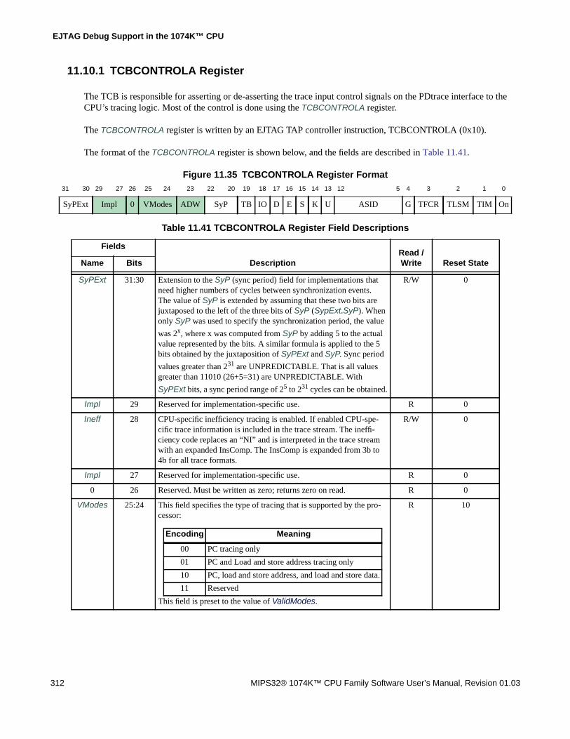
EJTAG Debug Support in the 1074K™ CPU
312 MIPS32® 1074K™ CPU Family Software User’s Manual, Revision 01.03
11.10.1 TCBCONTROLA Register
The TCB is responsible for asserting or de-asserting the trace input control signals on the PDtrace interface to theCPU’s tracing logic. Most of the control is done using the TCBCONTROLA register.
The TCBCONTROLA register is written by an EJTAG TAP controller instruction, TCBCONTROLA (0x10).
The format of the TCBCONTROLA register is shown below, and the fields are described in Table 11.41.
Figure 11.35 TCBCONTROLA Register Format31 30 29 27 26 25 24 23 22 20 19 18 17 16 15 14 13 12 5 4 3 2 1 0
SyPExt Impl 0 VModes ADW SyP TB IO D E S K U ASID G TFCR TLSM TIM On
Table 11.41 TCBCONTROLA Register Field Descriptions
Fields
DescriptionRead /Write Reset StateName Bits
SyPExt 31:30 Extension to the SyP (sync period) field for implementations thatneed higher numbers of cycles between synchronization events.The value of SyP is extended by assuming that these two bits arejuxtaposed to the left of the three bits of SyP (SypExt.SyP). Whenonly SyP was used to specify the synchronization period, the value
was 2x, where x was computed from SyP by adding 5 to the actualvalue represented by the bits. A similar formula is applied to the 5bits obtained by the juxtaposition of SyPExt and SyP. Sync period
values greater than 231 are UNPREDICTABLE. That is all valuesgreater than 11010 (26+5=31) are UNPREDICTABLE. With
SyPExt bits, a sync period range of 25 to 231 cycles can be obtained.
R/W 0
Impl 29 Reserved for implementation-specific use. R 0
Ineff 28 CPU-specific inefficiency tracing is enabled. If enabled CPU-spe-cific trace information is included in the trace stream. The ineffi-ciency code replaces an “NI” and is interpreted in the trace streamwith an expanded InsComp. The InsComp is expanded from 3b to4b for all trace formats.
R/W 0
Impl 27 Reserved for implementation-specific use. R 0
0 26 Reserved. Must be written as zero; returns zero on read. R 0
VModes 25:24 This field specifies the type of tracing that is supported by the pro-cessor:
This field is preset to the value of ValidModes.
R 10
Encoding Meaning
00 PC tracing only
01 PC and Load and store address tracing only
10 PC, load and store address, and load and store data.
11 Reserved

11.10 Trace Control Block (TCB) Registers (Hardware Control)
MIPS32® 1074K™ CPU Family Software User’s Manual, Revision 01.03 313
ADW 23 The data value width used in the trace formats: R 1
SyP 22:20 Used to indicate the synchronization period.The period (in cycles) between which the periodic synchronizationinformation is to be sent is defined as shown in the table below.
R/W 000
TB 19 Trace All Branches.When set to one, this field indicates that the CPU must trace eitherfull or incremental PC values for all branches. When set to zero,only the unpredictable branches are traced.
R/W Undefined
IO 18 Inhibit Overflow.This bit is used to indicate to the CPU trace logic that slow but com-plete tracing is desired. Hence, the CPU tracing logic must not allowa FIFO overflow and discard trace data. This is achieved by stallingthe pipeline when the FIFO is nearly full so that no trace records areever lost.
R/W Undefined
D 17 When set to one, this enables tracing in Debug mode, i.e., when theDM bit is one in the Debug register. For trace to be enabled inDebug mode, the On bit must be one and either the G bit must beone, or the current process must match the ASID field in this regis-ter.When set to zero, trace is disabled in Debug mode, irrespective ofother bits.
R/W Undefined
E 16 This controls when tracing is enabled. When set, tracing is enabledwhen either of the EXL or ERL bits in the Status register is one, pro-vided that the On bit (bit 0) is also set, and either the G bit is set, orthe current process ASID matches the ASID field in this register.
R/W Undefined
S 15 When set, this enables tracing when the CPU is in Supervisor modeas defined in the MIPS32 or MIPS64 architecture specification. Thisis provided the On bit (bit 0) is also set, and either the G bit is set, orthe current process ASID matches the ASID field in this register.
R/W Undefined
Table 11.41 TCBCONTROLA Register Field Descriptions (Continued)
Fields
DescriptionRead /Write Reset StateName Bits
Encoding Meaning
0 width is 16 bits
1 width is is 32 bits
SyP Sync Period
000 25
001 26
010 27
011 28
100 29
101 210
110 211
111 212

EJTAG Debug Support in the 1074K™ CPU
314 MIPS32® 1074K™ CPU Family Software User’s Manual, Revision 01.03
11.10.2 TCBCONTROLB Register
The TCB includes a second control register, TCBCONTROLB (0x11). This register generally controls what to do withthe trace information received.
The format of the TCBCONTROLB register is shown below, and the fields are described in Table 11.42.
K 14 When set, this enables tracing when the On bit is set and the CPU isin Kernel mode. Unlike the usual definition of Kernel Mode, this bitenables tracing only when the ERL and EXL bits in the Status reg-ister are zero. This is provided the On bit (bit 0) is also set, andeither the G bit is set, or the current process ASID matches theASID field in this register.
R/W Undefined
U 13 When set, this enables tracing when the CPU is in User mode asdefined in the MIPS32 or MIPS64 architecture specification. This isprovided the On bit (bit 0) is also set, and either the G bit is set, orthe current process ASID matches the ASID field in this register.
R/W Undefined
ASID 12:5 The ASID field to match when the G bit is zero. When the G bit isone, this field is ignored.
R/W Undefined
G 4 When set, this implies that tracing is to be enabled for all processes,provided that other enabling functions (like U, S, etc.,) are also true.
R/W Undefined
TFCR 3 When set, this indicates to the PDtrace interface that the optional Fcrbit must be traced in the appropriate trace formats. If PC tracing isdisabled, the full PC of the function call (or return) instruction mustalso be traced. Note that function call/return information is onlytraced if tracing is actually enabled for the current mode.
R/W Undefined
TLSM 2 When set, this indicates to the PDtrace interface that informationabout data cache misses should be traced. If PC, load/store addressesand data tracing are disabled (see TraceControlMode field), the fullPC and load/store address are traced for data cache misses. Ifload/store data tracing is enabled, the LSm bit must be traced in theappropriate trace format. Note that data cache miss information isonly traced if tracing is actually enabled for the current mode.
R/W Undefined
TIM 1 When set, this indicates to the PDtrace interface that the optional Imbit must be traced in the appropriate trace formats. If PC tracing isdisabled, the full PC of the instruction that missed in the I-cachemust be traced. Note that instruction cache miss information is onlytraced if tracing is actually enabled in the current mode.
R/W Undefined
On 0 This is the global trace enable switch to the CPU. When zero, trac-ing from the CPU is always disabled, unless enabled by CPU inter-nal software override.When set to one, tracing is enabled whenever the other enablingfunctions are also true.
R/W 0
Table 11.41 TCBCONTROLA Register Field Descriptions (Continued)
Fields
DescriptionRead /Write Reset StateName Bits

11.10 Trace Control Block (TCB) Registers (Hardware Control)
MIPS32® 1074K™ CPU Family Software User’s Manual, Revision 01.03 315
Figure 11.36 TCBCONTROLB Register Format31 30 28 27 26 25 21 20 19 18 17 16 15 14 13 12 11 10 8 7 6 3 2 1 0
WE 0 TWSrcWidth REG WR 0 TRPAD FDT RM TR BF TM TLSIF CR Cal TWSrcVal CA OfC EN
Table 11.42 TCBCONTROLB Register Field Descriptions
Fields
DescriptionRead /Write Reset StateName Bits
WE 31 Write Enable.Only when set to 1 will the other bits be written in TCBCONTROLB.This bit will always read 0.
R 0
0 30:28 Reserved. Must be written as zero; returns zero on read. R 0
TWSrcWidth 27:26 Used to indicate the number of bits used in the source field of the TraceWord, this is a configuration option of the CPU that cannot be modifiedby software.
This field can only be 10 for the 1074K CPU.
R 10
REG 25:21 Register select: This field select the registers accessible through theTCBDATA register. Legal values are shown in Table 11.40.
R/W 0
WR 20 Write Registers: When set, the register selected by REG field is readand written when TCBDATA is accessed. Otherwise the selected regis-ter is only read.
R/W 0
0 19 Reserved. Must be written as zero; returns zero on read. R 0
TRPAD 18 Trace RAM access disable bit, disables program software access to theon-chip trace RAM using load/store instructions. When this bit is set,that is, the access is disabled, then software access to the on-chip mem-ory is disabled. If probe access is not provided in the implementation,then this register bit must be tied to zero value to allow software to con-trol access.
R/W 0
FDT 17 Filtered Data Trace Mode enable bit. When the bit is 0, this mode isdisabled, reset value is disable. When set to 1, this mode is enabled.This mode is described in Section 11.8.13 “Filtered Data Trace Mode”
R/W 0
Encoding Meaning
00 Zero source field width
01 2- bit source field width
10 4- bit source field width
11 Reserved for future use

EJTAG Debug Support in the 1074K™ CPU
316 MIPS32® 1074K™ CPU Family Software User’s Manual, Revision 01.03
RM 16 Read on-chip trace memory.When written to 1, the read address-pointer of the on-chip memory isset to point to the oldest memory location written since the last reset ofpointers.Subsequent access to the TCBTW register (through theTCBDATA reg-ister), will automatically increment the read pointer (TCBRDP regis-ter) after each read. Note: The read pointer does not auto-increment ifthe WR field is one.When the write pointer is reached, this bit is automatically reset to 0,and the TCBTW register will read all zeros.Once set to 1, writing 1 again will have no effect. The bit is reset by set-ting the TR bit or by reading the last Trace word in TCBTW.This bit is reserved if on-chip memory is not implementedThis bit will affects trace memory only via the tcbcontrolb register thatresides in the CM.
R/W1 0
TR 15 Trace memory reset.When written to one, the address pointers for the on-chip trace memoryare reset to zero. Also the RM bit is reset to 0.This bit is automatically de-asserted back to 0 when the reset is com-pleted.This bit is reserved if on-chip memory is not implemented.This bit affects trace memory only via the TCBCONTROLB registerthat resides in the CM.
R/W1 0
BF 14 Buffer Full.Indicator used by the TCB to communicate to external software that theon-chip trace memory is being deployed in the trace-from andtrace-to mode. (See Section 11.14 “TCB On-Chip Trace Memory”)This bit is cleared when writing 1 to the TR bitThis bit is reserved if on-chip memory is not implemented.This bit reflects the state of the buffer, only via the tcbcontrolb registerthat resides in the CM.
R 0
Table 11.42 TCBCONTROLB Register Field Descriptions (Continued)
Fields
DescriptionRead /Write Reset StateName Bits

11.10 Trace Control Block (TCB) Registers (Hardware Control)
MIPS32® 1074K™ CPU Family Software User’s Manual, Revision 01.03 317
TM 13:12 Trace Mode. This field determines how the trace memory is filled whenusing the simple-break control in the PDtrace interface to start or stoptrace.
In Trace-To mode, the on-chip trace memory is filled, continuouslywrapping around and overwriting older Trace Words, as long as there istrace data coming from the CPU.In Trace-From mode, the on-chip trace memory is filled from the pointthat the CPU starts tracing until the on-chip trace memory is full.In both cases, de-asserting the EN bit in this register will also stop fillto the trace memory.If a TCBTRIGx trigger control register is used to start/stop tracing,then this field should be set to Trace-To mode.This bit is reserved if on-chip memory is not implemented.This field affects trace memory only via the tcbcontrolb register thatresides in the CM.
R/W 0
TLSIF 11 When set, this indicates to the TCB that information about Load andStore data cache miss, instruction cache miss, and function call are tobe taken from the PDtrace interface and trace them out in the appropri-ate trace formats as the three optional bits LSm, Im, and Fcr.
R/W 0
CR 10:8 Off-chip Clock Ratio. Writing this field, sets the ratio of the CPU clockto the off-chip trace memory interface clock. The clock-ratio encodingis shown in Table 11.43.Remark: As the Probe interface works in double data rate (DDR)mode, a 1:2 ratio indicates one data packet sent per CPU clock risingedge.This bit is reserved if off-chip trace option is not implemented.This field affects the Probe interface only via the tcbcontrolb registerthat resides in the CM.
R/W 100
Table 11.42 TCBCONTROLB Register Field Descriptions (Continued)
Fields
DescriptionRead /Write Reset StateName Bits
TM Trace Mode
00 Trace-To
01 Trace-From
10 Reserved
11 Reserved

EJTAG Debug Support in the 1074K™ CPU
318 MIPS32® 1074K™ CPU Family Software User’s Manual, Revision 01.03
Cal 7 Calibrate off-chip trace interface.If set to one, the off-chip trace pins will produce the following patternin consecutive trace clock cycles. If more than 4 data pins exist, the pat-tern is replicated for each set of 4 pins. The pattern repeats from top tobottom until the Cal bit is de-asserted.
Note: The clock source of the TCB and PIB must be running.This bit is reserved if off-chip trace option is not implemented.This field affects the Probe interface only via the tcbcontrolb registerthat resides in the CM.
R/W 0
TWSrcVal 6:3 These bits are used to indicate the value of the TW source field thatwill be traced if TWSrcWidth indicates a source bit-field width of 2 or4 bits. Note that if the field is 2 bits, then only bits 4:3 of this field willbe used in the TW.
R 0
CA 2 Cycle accurate trace.When set to 1, the trace will include stall information.When set to 0, the trace will exclude stall information, and remove bitzero from all transmitted TF’s.The stall information included/excluded is:• TF6 formats with TCBcode 0001 and 0101.• All TF1 formats.
R/W 0
OfC 1 If set to 1, trace is sent to off-chip memory using TR_DATA pins.If set to 0, trace info is sent to on-chip memory.This bit is read only if a single memory option exists (either off-chip oron-chip only).This field affects trace only via the tcbcontrolb register that resides inthe CM.
R/W Preset
Table 11.42 TCBCONTROLB Register Field Descriptions (Continued)
Fields
DescriptionRead /Write Reset StateName Bits
Calibra ions pattern
3 2 1 0
Thi
s pa
ttern
is r
eplic
ated
for
ever
y 4
bits
ofT
RD
AT
Api
ns.
0 0 0 0
1 1 1 1
0 0 0 0
0 1 0 1
1 0 1 0
1 0 0 0
0 1 0 0
0 0 1 0
0 0 0 1
1 1 1 0
1 1 0 1
1 0 1 1
0 1 1 1

11.10 Trace Control Block (TCB) Registers (Hardware Control)
MIPS32® 1074K™ CPU Family Software User’s Manual, Revision 01.03 319
11.10.3 TCBDATA Register
The TCBDATA register (0x12) is used to access the registers defined by the TCBCONTROLBREG field; see Table11.40. Regardless of which register or data entry is accessed through TCBDATA, the register is only written if theTCBCONTROLBWR bit is set. For read-only registers, the TCBCONTROLBWR is a don’t care. If software is accessingthe on-chip trace memory to read out the trace words, then TCBDATA is not used for the indirect read of the TCBTW.Instead software can read from TCBTW directly.
The format of the TCBDATA register is shown below, and the field is described in Table 11.44. The width of TCBDATAis 64 bits when on-chip trace words (TWs) are accessed (TCBTW access).
Figure 11.37 TCBDATA Register Format
EN 0 Enable trace.This is the master enable for trace to be generated from the TCB. Thisbit can be set or cleared, either by writing this register or from astart/stop/about trigger.When set to 1, trace information is sampled on the output pins (of thecapture-to-compression interface) or written in the on-chip trace mem-ory. Trace Words are generated and sent to either on-chip memory or tothe Trace Probe. The target of the trace is selected by the OfC bit.When set to 0, trace information on the output pins are ignored. Apotential TF6-stop (from a stop trigger) is generated as the last infor-mation, the TCB pipeline is flushed, and trace output is stopped.
R/W 0
Table 11.43 Clock Ratio encoding of the CR field
CR/CRMin/CRMax Clock Ratio
000 8:1 (Trace clock is eight times that of CPU clock)
001 4:1 (Trace clock is four times that of CPU clock)
010 2:1 (Trace clock is double that of CPU clock)
011 1:1 (Trace clock is same as CPU clock)
100 1:2 (Trace clock is one half of CPU clock)
101 1:4 (Trace clock is one fourth of CPU clock)
110 1:6 (Trace clock is one sixth of CPU clock)
111 1:8 (Trace clock is one eighth of CPU clock)
31(63) 0
Data
Table 11.42 TCBCONTROLB Register Field Descriptions (Continued)
Fields
DescriptionRead /Write Reset StateName Bits
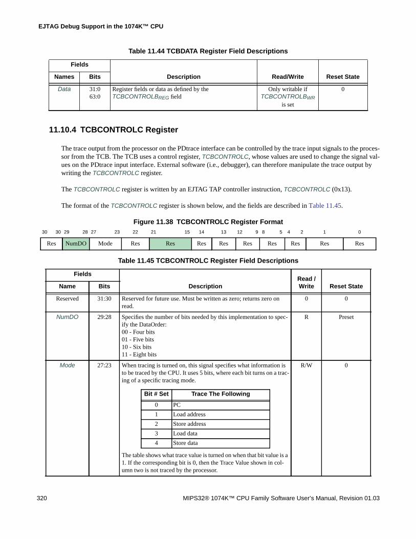
EJTAG Debug Support in the 1074K™ CPU
320 MIPS32® 1074K™ CPU Family Software User’s Manual, Revision 01.03
11.10.4 TCBCONTROLC Register
The trace output from the processor on the PDtrace interface can be controlled by the trace input signals to the proces-sor from the TCB. The TCB uses a control register, TCBCONTROLC, whose values are used to change the signal val-ues on the PDtrace input interface. External software (i.e., debugger), can therefore manipulate the trace output bywriting the TCBCONTROLC register.
The TCBCONTROLC register is written by an EJTAG TAP controller instruction, TCBCONTROLC (0x13).
The format of the TCBCONTROLC register is shown below, and the fields are described in Table 11.45.
Figure 11.38 TCBCONTROLC Register Format
Table 11.44 TCBDATA Register Field Descriptions
Fields
Description Read/Write Reset StateNames Bits
Data 31:063:0
Register fields or data as defined by theTCBCONTROLBREG field
Only writable ifTCBCONTROLBWR
is set
0
30 30 29 28 27 23 22 21 15 14 13 12 9 8 5 4 2 1 0
Res NumDO Mode Res Res Res Res Res Res Res Res Res
Table 11.45 TCBCONTROLC Register Field Descriptions
Fields
DescriptionRead /Write Reset StateName Bits
Reserved 31:30 Reserved for future use. Must be written as zero; returns zero onread.
0 0
NumDO 29:28 Specifies the number of bits needed by this implementation to spec-ify the DataOrder:00 - Four bits01 - Five bits10 - Six bits11 - Eight bits
R Preset
Mode 27:23 When tracing is turned on, this signal specifies what information isto be traced by the CPU. It uses 5 bits, where each bit turns on a trac-ing of a specific tracing mode.
The table shows what trace value is turned on when that bit value is a1. If the corresponding bit is 0, then the Trace Value shown in col-umn two is not traced by the processor.
R/W 0
Bit # Set Trace The Following
0 PC
1 Load address
2 Store address
3 Load data
4 Store data

11.10 Trace Control Block (TCB) Registers (Hardware Control)
MIPS32® 1074K™ CPU Family Software User’s Manual, Revision 01.03 321
11.10.5 TCBCONTROLD Register
The TCB includes a control register, TCBCONTROLD, whose values are used to control the tracing functions of theCoherence Manager. External software (i.e., debugger) can therefore manipulate the trace output by writing to thisregister. Though each of the CPUs in the 1074K Coherent Processing System will have this register, the only fieldused by the CM is the Core_CM_En field. The TCBCONTROLD located within the CM controls the tracing func-tions of the CM.
The TCBCONTROLD register is written by an EJTAG TAP controller instruction, TCBCONTROLD (0x14).
The format of the TCBCONTROLD register is shown below, and the fields are described in Table 11.46.
Figure 11.39 TCBCONTROLD Register Format
Res 22:0 Reserved for future use. Must be written as zero; returns zero onread.
0 0
31 26 25 24 23 22 21 20 19 18 17 16 15 12 9 8 5 4 3 2 1 0
Reserved P4_Ctl P3_Ctl P2_Ctl P1_Ctl P0_Ctl Reserved TWSrcVal WB IO TLev AE C_En En
Table 11.46 TCBCONTROLD Register Field Descriptions
Fields
DescriptionRead /Write Reset StateName Bits
Res 31:26,15:12,
6
Reserved for future use. Must be written as zero; returns zero onread.
0 0
P4_Ctl 25:24 Trace control for port 4. See Table 11.47 R/W 11
P3_Ctl 23:22 Trace control for port 3. See Table 11.47 R/W 11
P2_Ctl 21:20 Trace control for port 2. See Table 11.47 R/W 11
P1_Ctl 19:18 Trace control for port 1. See Table 11.47 R/W 11
P0_Ctl 17:16 Trace control for port 0. See Table 11.47 R/W 11
TWSrcVal 11:8 Identifier to be included in trace words that come from the CM R/W 0000
WB 7 When set, coherent writeback transactions will be traced R/W 0
IO 5 Inhibit Overflow: When set, the CM will stall rather than allowingthe trace FIFO to overflow and lose information
R/W 0
TLev 4:3 Trace Level - controls how much information is being traced R/W 00
Table 11.45 TCBCONTROLC Register Field Descriptions (Continued)
Fields
DescriptionRead /Write Reset StateName Bits
Encoding Description
00 Default, no timing information
11 Include info on stall lengths and causes
1x Reserved

EJTAG Debug Support in the 1074K™ CPU
322 MIPS32® 1074K™ CPU Family Software User’s Manual, Revision 01.03
11.10.6 TCBCONTROLE Register
The trace output from the processor on the PDtrace interface can be controlled by the trace input signals to the proces-sor from the TCB. The TCB uses a control register, TCBCONTROLE, whose values are used to change the signal val-ues on the PDtrace input interface. External software (i.e., debugger), can therefore manipulate the trace output bywriting the TCBCONTROLE register.
The TCBCONTROLE register is written by an EJTAG TAP controller instruction, TCBCONTROLE (0x16).
The format of the TCBCONTROLE register is shown below, and the fields are described in Table 11.48.
Figure 11.40 TCBCONTROLE Register Format
AE 2 Address Enable. When set, addresses will be traced for all ports.When cleared, address tracing can be individually enabled via thePx_Ctl fields.
R/W 0
CEn 1 Core_CM_Enable: The CM looks at this bit coming from each ofthe CPUs. Allows CPUs other than the master to enable tracing ifother conditions are met.
R/W 0
En 0 Enable: Overall enable for tracing from the CM. R/W 0
Table 11.47 Port Control Values
Value Meaning
00 Tracing enabled. No address tracing.
01 Tracing enabled including address tracing.
10 Reserved
11 Tracing disabled.
31 9 8 7 6 5 4 3 2 1 0
0 TdIDLE 0 PecOvf PeCFCR PeCBP PeCSync PeCE PeC
Table 11.48 TCBCONTROLE Register Field Descriptions
Fields
DescriptionRead /Write Reset StateName Bits
0 31:9 Reserved for future use. Must be written as zero; returnszero on read.
0 0
TrIDLE 8 Trace Unit Idle. This bit indicates if the trace hardware iscurrently idle (not processing any data). This can be usefulwhen switching control of trace from hardware to softwareand vice versa. The bit is read-only and updated by thetrace hardware.
R 1
Table 11.46 TCBCONTROLD Register Field Descriptions (Continued)
Fields
DescriptionRead /Write Reset StateName Bits
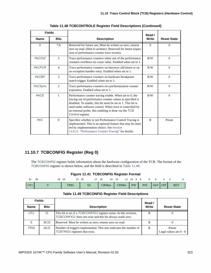
11.10 Trace Control Block (TCB) Registers (Hardware Control)
MIPS32® 1074K™ CPU Family Software User’s Manual, Revision 01.03 323
11.10.7 TCBCONFIG Register (Reg 0)
The TCBCONFIG register holds information about the hardware configuration of the TCB. The format of theTCBCONFIG register is shown below, and the field is described in Table 11.49.
Figure 11.41 TCBCONFIG Register Format
0 7:6 Reserved for future use; Must be written as zero; returnszero on read. (Hint to architect, Reserved for future expan-sion of performance counter trace events).
0 0
PeCOvf 5 Trace performance counters when one of the performancecounters overflows its count value. Enabled when set to 1.
R/W 0
PeCFCR 4 Trace performance counters on function call/return or onan exception handler entry. Enabled when set to 1.
R/W 0
PeCBP 3 Trace performance counters on hardware breakpointmatch trigger. Enabled when set to 1.
R/W 0
PeCSync 2 Trace performance counters on synchronization counterexpiration. Enabled when set to 1.
R/W 0
PeCE 1 Performance counter tracing enable. When set to 0, thetracing out of performance counter values as specified isdisabled. To enable, this bit must be set to 1. This bit isused under software control. When trace is controlled byan external probe, this enabling is done via the TCBControl register.
R/W 0
PeC 0 Specifies whether or not Performance Control Tracing isimplemented. This is an optional feature that may be omit-ted by implementation choice. See Section11.8.12 “Performance Counter Tracing” for details.
R Preset
31 30 25 24 21 20 17 16 14 13 11 10 9 8 6 5 4 3 0
CF1 0 TRIG SZ CRMax CRMin PW PiN OnT OfT REV
Table 11.49 TCBCONFIG Register Field Descriptions
Fields
DescriptionRead /Write Reset StateName Bits
CF1 31 This bit is set if a TCBCONFIG1 register exists. In this revision,TCBCONFIG1 does not exist and this bit always reads zero.
R 0
0 30:25 Reserved. Must be written as zero; returns zero on read. R 0
TRIG 24:21 Number of triggers implemented. This also indicates the number ofTCBTRIGx registers that exist.
R PresetLegal values are 0 - 8
Table 11.48 TCBCONTROLE Register Field Descriptions (Continued)
Fields
DescriptionRead /Write Reset StateName Bits

EJTAG Debug Support in the 1074K™ CPU
324 MIPS32® 1074K™ CPU Family Software User’s Manual, Revision 01.03
11.10.8 TCBTW Register (Reg 4)
The TCBTW register is used to read Trace Words from the on-chip trace memory. Accesses to the memory will beallowed only via the TCBTW register that resides in the CM.The Trace Word (TW) read is the one pointed to by theTCBRDP register. A side effect of reading the TCBTW register is that the TCBRDP register increments to the next TWin the on-chip trace memory. If TCBRDP is at the max size of the on-chip trace memory, the increment wraps back toaddress zero. The TCBTW register is mapped to offset 0x3100 in drseg. An access to offset 0x3100 automaticallycauses the read pointer to be incremented. The use of load half-word or load byte instructions can lead to unpredict-
SZ 20:17 On-chip trace memory size. This field holds the encoded size of theon-chip trace memory.
The size in bytes is given by 2(SZ+8), implying that the minimum sizeis 256 bytes and the largest is 8Mb.This bit is reserved if on-chip memory is not implemented.
R Preset
CRMax 16:14 Off-chip Maximum Clock Ratio.This field indicates the maximum ratio of the CPU clock to theoff-chip trace memory interface clock. The clock-ratio encoding isshown in Table 11.43.This bit is reserved if off-chip trace option is not implemented.
R Preset
CRMin 13:11 Off-chip Minimum Clock Ratio.This field indicates the minimum ratio of the CPU clock to theoff-chip trace memory interface clock.The clock-ratio encoding isshown in Table 11.43.This bit is reserved if off-chip trace option is not implemented.
R Preset
PW 10:9 Probe Width: Number of bits available on the off-chip trace interfaceTR_DATA pins. The number of TR_DATA pins is encoded, asshown in the table.
This field is preset based on input signals to the TCB and the actualcapability of the TCB.This bit is reserved if off-chip trace option is not implemented.
R Preset
PiN 8:6 Pipe number.Indicates the number of execution pipelines.
R 0
OnT 5 When set, this bit indicates that on-chip trace memory is present.This bit is preset based on the selected option when the TCB isimplemented.
R Preset
OfT 4 When set, this bit indicates that off-chip trace interface is present.This bit is preset based on the selected option when the TCB isimplemented, and on the existence of a PIB module(TC_PibPresent asserted).
R Preset
REV 3:0 Revision of TCB. R 2
Table 11.49 TCBCONFIG Register Field Descriptions (Continued)
Fields
DescriptionRead /Write Reset StateName Bits
PW Number of bits used on TR_DATA
00 4 bits
01 8 bits
10 16 bits
11 Reserved

11.10 Trace Control Block (TCB) Registers (Hardware Control)
MIPS32® 1074K™ CPU Family Software User’s Manual, Revision 01.03 325
able results, and is not recommended. The results of attempting to write to trace memory by an explicit store instruc-tion targeting TCBTW are unpredictable.
This register is reserved if on-chip trace memory is not implemented.
The format of the TCBTW register is shown below, and the field is described in Table 11.50.
Figure 11.42 TCBTW Register Format
11.10.9 TCBRDP Register (Reg 5)
The TCBRDP register is the address pointer to on-chip trace memory. It points to the TW read when reading theTCBTW register. When writing the TCBCONTROLBRM bit to 1, this pointer is reset to the current value of TCBSTP.
This register is reserved if on-chip trace memory is not implemented.
The format of the TCBRDP register is shown below, and the field is described in Table 11.51. The value of n dependson the size of the on-chip trace memory. As the address points to a 64-bit TW, lower three bits are always zero.
Figure 11.43 TCBRDP Register Format
11.10.10 TCBWRP Register (Reg 6)
The TCBWRP register is the address pointer to on-chip trace memory. It points to the location where the next new TWfor on-chip trace will be written.
This register is reserved if on-chip trace memory is not implemented.
63 0
Data
Table 11.50 TCBTW Register Field Descriptions
Fields
DescriptionRead /Write Reset StateNames Bits
Data 63:0 Trace Word (TW) R/W 0
31 n+1 n 0
Address
Table 11.51 TCBRDP Register Field Descriptions
Fields
DescriptionRead /Write Reset StateNames Bits
Data 31:(n+1) Reserved. Must be written zero, reads back zero. 0 0
Address n:0 Byte address of on-chip trace memory word. R/W 0

EJTAG Debug Support in the 1074K™ CPU
326 MIPS32® 1074K™ CPU Family Software User’s Manual, Revision 01.03
The format of the TCBWRP register is shown below, and the fields are described in Table 11.52. The value of ndepends on the size of the on-chip trace memory. As the address points to a 64-bit TW, the lower three bits are alwayszero.
Figure 11.44 TCBWRP Register Format
11.10.11 TCBSTP Register (Reg 7)
The TCBSTP register is the start pointer register. This register points to the on-chip trace memory address at whichthe oldest TW is located. This pointer is reset to zero when the TCBCONTROLBTR bit is written to 1. If a continuoustrace to on-chip memory wraps around the on-chip memory, TSBSTP will have the same value as TCBWRP.
This register is reserved if on-chip trace memory is not implemented.
The format of the TCBSTP register is shown below, and the fields are described in Table 11.53. The value of ndepends on the size of the on-chip trace memory. As the address points to a 64-bit TW, lower three bits are alwayszero.
Figure 11.45 TCBSTP Register Format
11.10.12 TCBTRIGx Register (Reg 16-23)
Up to eight Trigger Control registers are possible. Each register is named TCBTRIGx, where x is a single digit numberfrom 0 to 7 (TCBTRIG0 is Reg 16). The actual number of trigger registers implemented is defined in theTCBCONFIGTRIG field. An unimplemented register will read all zeros and writes are ignored.
Each Trigger Control register controls when an associated trigger is fired, and the action to be taken when the triggeroccurs. Please also read Section 11.12 “TCB Trigger Logic”, for detailed description of trigger logic issues.
31 n+1 n 0
Address
Table 11.52 TCBWRP Register Field Descriptions
Fields
DescriptionRead /Write Reset StateNames Bits
Data 31:(n+1) Reserved. Must be written zero, reads back zero. 0 0
Address n:0 Byte address of on-chip trace memory word. R/W 0
31 n+1 n 0
0 Address
Table 11.53 TCBSTP Register Field Descriptions
Fields
DescriptionRead /Write Reset StateNames Bits
Data 31:(n+1) Reserved. Must be written zero, reads back zero. 0 0
Address n:0 Byte address of on-chip trace memory word. R/W 0

11.10 Trace Control Block (TCB) Registers (Hardware Control)
MIPS32® 1074K™ CPU Family Software User’s Manual, Revision 01.03 327
The format of the TCBTRIGx register is shown below, and the fields are described in Table 11.54.
Figure 11.46 TCBTRIGx Register Format31 24 23 22 16 15 14 13 7 6 5 4 3 2 1 0
TCBinfo Trace 0 CHTro PDTro 0 DM CHTri PDTri Type FO TR
Table 11.54 TCBTRIGx Register Field Descriptions
Fields
DescriptionRead /Write Reset StateNames Bits
TCBinfo 31:24 TCBinfo to be used in a possible TF6 trace format when this triggerfires.
R/W 0
Trace 23 When set, generate TF6 trace information when this trigger fires.Use TCBinfo field for the TCBinfo of TF6 and use Type field for thetwo MSB of the TCBtype of TF6. The two LSB of TCBtype are 00.The write value of this bit always controls the behavior of this trig-ger.When this trigger fires, the read value will change to indicate if theTF6 format was ever suppressed by a simultaneous trigger. If so, theread value will be 0. If the write value was 0, the read value isalways 0. This special read value is valid until the TCBTRIGx regis-ter is written.
R/W 0
0 22:16 Reserved. Must be written as zero; returns zero on read. R 0
CHTro 15 When set, generate a single cycle strobe on TC_ChipTrigOut whenthis trigger fires.
R/W 0
PDTro 14 When set, generate a single cycle strobe on TC_ProbeTrigOutwhen this trigger fires.
R/W 0
0 13:7 Reserved. Must be written as zero; returns zero on read. R 0
DM 6 When set, this Trigger will fire when a rising edge on the Debugmode indication from the CPU is detected.The write value of this bit always controls the behavior of this trig-ger.When this trigger fires, the read value will change to indicate if thissource was ever the cause of a trigger action (even if the action wassuppressed). If so the read value will be 1. If the write value was 0the read value is always 0. This special read value is valid until theTCBTRIGx register is written.
R/W 0
CHTri 5 When set, this Trigger will fire when a rising edge onTC_ChipTrigIn is detected.The write value of this bit always controls the behavior of this trig-ger.When this trigger fires, the read value will change to indicate if thissource was ever the cause of a trigger action (even if the action wassuppressed). If so the read value will be 1. If the write value was 0the read value is always 0. This special read value is valid until theTCBTRIGx register is written.
R/W 0

EJTAG Debug Support in the 1074K™ CPU
328 MIPS32® 1074K™ CPU Family Software User’s Manual, Revision 01.03
PDTri 4 When set, this Trigger will fire when a rising edge onTC_ProbeTrigIn is detected.The write value of this bit always controls the behavior of this trig-ger.When this trigger fires, the read value will change to indicate if thissource was ever the cause of a trigger action (even if the action wassuppressed). If so the read value will be 1. If the write value was 0the read value is always 0. This special read value is valid until theTCBTRIGx register is written.
R/W 0
Type 3:2 Trigger Type: The Type indicates the action to take when this triggerfires. The table below show the Type values and the Trigger action.
The actual action is to set or clear the TCBCONTROLBEN bit. AStart trigger will set TCBCONTROLBEN, a End trigger will clearTCBCONTROLBEN. The About trigger will clearTCBCONTROLBEN half way through the trace memory, from thetrigger. The size determined by the TCBCONFIGSZ field foron-chip memory. Or from the TCBCONTROLASyP field foroff-chip trace.If Trace is set, then a TF6 format is added to the trace words. ForStart and Info triggers this is done before any other TF’s in that samecycle. For End and About triggers, the TF6 format is added after anyother TF’s in that same cycle.If the TCBCONTROLBTM field is implemented, it must be set toTrace-To mode (00), for the Type field to control on-chip trace fill.The write value of this bit always controls the behavior of this trig-ger.When this trigger fires, the read value will change to indicate if thetrigger action was ever suppressed. If so the read value will be 11. Ifthe write value was 11 the read value is always 11. This special readvalue is valid until the TCBTRIGx register is written.
R/W 0
FO 1 Fire Once. When set, this trigger will not re-fire until the TR bit isde-asserted. When de-asserted, this trigger will fire each time one ofthe trigger sources indicates trigger.
R/W 0
Table 11.54 TCBTRIGx Register Field Descriptions (Continued)
Fields
DescriptionRead /Write Reset StateNames Bits
Type Trigger action
00 Trigger Start: Trigger start-point of trace.
01 Trigger End: Trigger end-point of trace.
10 Trigger About: Trigger center-point of trace.
11 Trigger Info: No action trigger, only for trace info.

11.11 Enabling MIPS Trace
MIPS32® 1074K™ CPU Family Software User’s Manual, Revision 01.03 329
11.10.13 Register Reset State
Reset state for all register fields is entered when either of the following occur:
1. TAP controller enters/is in Test-Logic-Reset state.
2. EJ_TRST_N input is asserted low.
11.11 Enabling MIPS Trace
As there are several ways to enable tracing, it can be quite confusing to figure out how to turn tracing on and off. Thissection should help clarify the enabling of trace.
11.11.1 Trace Trigger from EJTAG Hardware Instruction/Data Breakpoints
If hardware instruction/data simple breakpoints are implemented in the 1074K CPU, then these breakpoint can beused as triggers to start/stop trace. When used for this, the breakpoints need not also generate a debug exception, butare capable of only generating an internal trigger to the trace logic. This is done by only setting the TE bit and not theBE bit in the Breakpoint Control register. Please see Section 11.2.8.5 “Instruction Breakpoint Control n (IBCn)Register” and Section 11.2.9.5 “Data Breakpoint Control n (DBCn) Register” for details on breakpoint control.
In connection with the breakpoints, the Trace BreakPoint Control (TraceBPC) register is used to define the trace actionwhen a trigger happens. When a breakpoint is enabled as a trigger (TE = 1), it can be selected to be either a start or astop trigger to the trace logic. Please see sections Section 7.2.35 “TraceIBPC Register (CP0 Register 23, Select 4)”and Section 7.2.36 “TraceDBPC Register (CP0 Register 23, Select 5)” for details on how to define a start/stop trig-ger.
The trace triggers are best used for fine grain tracing. First the mode in which the fine grain tracing is desired shouldbe disabled in the TraceControl. For example if fine grain tracing is to be done in User Mode then TraceControlU is setto zero. This disables general tracing while the program is in User Mode. Then a breakpoint start trigger turns on thetrace at a particular instruction, and a breakpoint off trigger turns off the trace at the desired ending instruction. Thebreakpoint trigger can be caused by a breakpoint address match or a breakpoint data match. Both precise and impre-cise data match is supported. The imprecise data match will generate the trace trigger after the expected start/endpoint, as the imprecise data match is dependent on system latencies.
TR 0 Trigger happened. When set, this trigger fired since the TR bit waslast written 0.This bit is used to inspect whether the trigger fired since this bit waslast written zero.When set, all the trigger source bits (bit 4 to 13) will change theirread value to indicate if the particular bit was the source to fire thistrigger. Only enabled trigger sources can set the read value, but morethan one is possible.Also when set the Type field and the Trace field will have read val-ues which indicate if the trigger action was ever suppressed by ahigher priority trigger.
R/W0 0
Table 11.54 TCBTRIGx Register Field Descriptions (Continued)
Fields
DescriptionRead /Write Reset StateNames Bits

EJTAG Debug Support in the 1074K™ CPU
330 MIPS32® 1074K™ CPU Family Software User’s Manual, Revision 01.03
11.11.2 Turning On PDtrace™ Trace
Trace enabling and disabling from software is similar to the hardware method, except that the bits in the control reg-ister are used instead of the input enable signals from the TCB. The TraceControlTS bit controls whether hardware(via the TCB), or software (via the TraceControl register) controls tracing functionality.
Trace is turned on when the following expression evaluates true:
((
(TraceControlTS and TraceControlOn) or((not TraceControlTS) and TCBCONTROLAOn)
)and(MatchEnable or TriggerEnable)
)
where,
MatchEnable ←(
TraceControlTSand(
TraceControlG or(((TraceControlASID xor EntryHiASID) and (not TraceControlASID_M)) = 0)
)and(
(TraceControlU and UserMode) or(TraceControlS and SupervisorMode) or(TraceControlK and KernelMode) or(TraceControlE and ExceptionMode) or(TraceControlD and DebugMode)
))or(
(not TraceControlTS)and(TCBCONTROLAG or (TCBCONTROLAASID = EntryHiASID))and(
(TCBCONTROLAU and UserMode) or(TCBCONTROLAS and SupervisorMode) or(TCBCONTROLAK and KernelMode) or(TCBCONTROLAE and ExceptionMode) or(TCBCONTROLADM and DebugMode)
))
and where,
TriggerEnable ←(
DBCiTE andDBSBS[i] and

11.11 Enabling MIPS Trace
MIPS32® 1074K™ CPU Family Software User’s Manual, Revision 01.03 331
TraceBPCDE and(TraceBPCDBPOn[i] = 1)
)or(
IBCiTE andIBSBS[i] andTraceBPCIE and(TraceBPCIBPOn[i] = 1)
)
As seen in the expression above, trace can be turned on only if the master switch TraceControlOn orTCBCONTROLAOn is first asserted.
Once this is asserted, there are two ways to turn on tracing. The first way, the MatchEnable expression, uses the inputenable signals from the TCB or the bits in the TraceControl register. This tracing is done over general program areas.For example, all of the user-level code for a particular process (if ASID is specified), and so on.
The second way to turn on tracing, the TriggerEnable expression, is from the processor side using the EJTAG hard-ware breakpoint triggers. If EJTAG is implemented, and hardware breakpoints can be set, then using this methodenables finer grain tracing control. It is possible to send a trigger signal that turns on tracing at a particular instruction.For example, it would be possible to trace a single procedure in a program by triggering on trace at the first instruc-tion, and triggering off trace at the last instruction.
The easiest way to unconditionally turn on trace is to assert either hardware or software tracing and the correspondingtrace on signal with other enables. For example, with TraceControlTS=0, i.e., hardware controlled tracing, assertTCBCONTROLAOn, TCBCONTROLAG, and all the other signals in the second part of expression MatchEnable. Toonly trace when a particular process with a particular ASID is executing, assert TCBCONTROLAOn, the correctTCBCONTROLAASID value, and the TCBCONTROLAU, TCBCONTROLAK, TCBCONTROLAE, andTCBCONTROLADM registers. (If it is known that the particular process is a user-level process, then it would be suffi-cient to only assert TCBCONTROLAU for example). When using the EJTAG hardware triggers to turn trace on andoff, it is best if TCBCONTROLAOn is asserted with all the other processor mode selection bits in TCBCONTROLA areturned off. This would be the least confusing way to control tracing with the trigger signals. In a similar manner, trac-ing can be controlled via software with the TraceControl register.
11.11.3 Turning Off PDtrace™ Trace
Trace is turned off when the following expression evaluates true:
((TraceControlTS and (not TraceControlOn))) or((not TraceControlTS) and (not TCBCONTROLAOn))
)or(
(not MatchEnable) and(not TriggerEnable) andTriggerDisable
)
where,
TriggerDisable ←(
DBCiTE and

EJTAG Debug Support in the 1074K™ CPU
332 MIPS32® 1074K™ CPU Family Software User’s Manual, Revision 01.03
DBSBS[i] andTraceBPCDE and(TraceBPCDBPOn[i] = 0)
)or(
IBCiTE andIBSBS[i] andTraceBPCIE and(TraceBPCIBPOn[i] = 0)
)
Tracing can be unconditionally turned off by de-asserting the TraceControlOn bit or the TCBCONTROLAOn signal.When either of these are asserted, tracing can be turned off if all of the enables are de-asserted, regardless of theTraceControlG bit (TCBCONTROLAG) and TraceControlASID (TCBCONTROLAASID) values. EJTAG hardware break-points can be used to trigger trace off as well.
Note that if simultaneous triggers are generated, and even one of them turns on tracing, then even if all of the othersattempt to trigger trace off, tracing will still be turned on. This condition is reflected in presence of the “(not Trigger-Enable)” term in the expression above.
11.11.4 TCB Trace Enabling
The TCB must be enabled in order to produce a trace on the probe or to on-chip memory, when trace information issent on the PDtrace interface. The main switch for this is the TCBCONTROLBEN bit. When set, the TCB will sendtrace information to either on-chip trace memory or to the Trace Probe, as controlled by the setting of theTCBCONTROLBOfC bit.
The TCB can optionally include trigger logic, which can control the TCBCONTROLBEN bit. Please see Section11.12 “TCB Trigger Logic” for details.
11.11.5 Tracing a Reset Exception
Tracing a reset exception is possible. However, the TraceControlTS bit is reset to 0 at CPU reset, so all the trace controlmust be from the TCB (using TCBCONTROLA and TCBCONTROLB). The PDtrace FIFO and the entire TCB arereset based on an EJTAG reset. It is thus possible to set up the trace modes, etc., using the TAP controller, and thenreset the CPU.
11.12 TCB Trigger Logic
The TCB is optionally implemented with a trigger unit, which is indicated by a non-zero value in theTCBCONFIGTRIG. This subsection will explain some of the issues around triggers in the TCB.
11.12.1 Trigger Units Overview
TCB trigger logic features three main parts:
1. Common Trigger Source detection unit
2. 1 to 8 separate Trigger Control units
3. Common Trigger Action unit


EJTAG Debug Support in the 1074K™ CPU
334 MIPS32® 1074K™ CPU Family Software User’s Manual, Revision 01.03
11.12.3 Trigger Control Units
Up to eight Trigger Control Units are possible. Each of them has its own Trigger Control Register (TCBTRIGx,x={0..7}). Each of these registers controls the trigger fire mechanism for the unit. Each unit has all of the TriggerSources as possible trigger events, and they can fire one or more of the Trigger Actions, as explained in the descrip-tion of the Trigger Control register TCBTRIGx (Section 11.10.12 “TCBTRIGx Register (Reg 16-23)”).
11.12.4 Trigger Action Unit
The TCB has four possible trigger actions:
1. Chip-level trigger output (TC_ChipTrigOut)
2. Probe trigger output (TR_TRIGOUT)
3. Trace information. Put a programmable byte into the trace stream from the TCB.
4. Start, End, or About (delayed end) control of the TCBCONTROLBEN bit
The basic function of the trigger actions is explained in Section 11.10.12 “TCBTRIGx Register (Reg 16-23)”. Seealso Section 11.12.5 “Simultaneous Triggers”.
11.12.5 Simultaneous Triggers
Two or more triggers can fire simultaneously. The resulting behavior depends on the trigger action set for each. andwhether or not they should produce a TF6 trace information output. There are two groups of trigger actions: Priori-tized and OR’ed.
11.12.5.1 Prioritized Trigger Actions
For simultaneous prioritized trigger actions, the trigger control unit which has the lowest number takes precedenceover the higher numbered units. The x in TCBTRIGx registers defines the number. The oldest trigger takes precedenceover all others.
The following trigger actions are prioritized when two or more units fire simultaneously:
• Trigger Start, End and About type triggers (TCBTRIGxType field set to 00, 01 or 10), which will assert/de-assertthe TCBCONTROLBEN bit. The About trigger is delayed and will always change TCBCONTROLBEN because it isthe oldest trigger when it de-asserts TCBCONTROLBEN. An About trigger will not start the countdown if an evenolder About trigger is using the Trace Word counter.
• Triggers which produce TF6 trace information in the trace flow (Trace bit is set).
Regardless of priority, the TCBTRIGxTR bit is set when the trigger fires, even if a trigger action is suppressed by ahigher priority trigger action. If the trigger is set to only fire once (the TCBTRIGxFO bit is set), then the suppressedtrigger action will not happen until after the TCBTRIGxTR is cleared.
If a Trigger action is suppressed by a higher priority trigger, then the read value, when the TCBTRIGxTR bit is set, forthe TCBTRIGxTrace field will be 0 for suppressed TF6 trace information actions. The read value in the TCBTRIGxType
field for suppressed Start/End/About triggers will be 11. This indication of a suppressed action is sticky. If any of thetwo actions (Trace and Type) are ever suppressed for a multi-fire trigger (the TCBTRIGxFO bit is zero), then the readvalues in Trace and/or Type are set to indicate any suppressed action.

11.13 MIPS Trace Cycle-by-Cycle Behavior
MIPS32® 1074K™ CPU Family Software User’s Manual, Revision 01.03 335
About Trigger
The About triggers delayed de-assertion of the TCBCONTROLBEN bit is always executed, regardless of priority fromanother Start trigger at the time of the TCBCONTROLBEN change. This means that if a simultaneous About triggeraction on the TCBCONTROLBEN bit (n/2 Trace Words after the trigger) and a Start trigger hit the same cycle, then theAbout trigger wins, regardless of which trigger number it is. The oldest trigger takes precedence.
However, if an About trigger has started the count down from n/2, but not yet reached zero, then a new About triggerwill NOT be executed. Only one About trigger can have the cycle counter. This second About trigger will store 11 inthe TCBTRIGxType field. But, if the TCBTRIGxTrace bit is set, a TF6 trace information will still go in the trace.
11.12.5.2 OR’ed Trigger Actions
The simple trigger actions CHTro and PDTro from each trigger unit, are OR’ed together to produce the final trigger.One or more expected trigger strobes on TC_ChipTrigOut can thus disappear. External logic should not rely on thecounting of strobes to predict a specific event, unless simultaneous triggers are known not to occur.
11.13 MIPS Trace Cycle-by-Cycle Behavior
A key reason for using trace to debug a software problem, rather than using single stepping, is to get an accurate pic-ture of real-time behavior. However, the trace logic itself can, when enabled, affect the exact cycle-by-cycle behavior.
11.13.1 FIFO Logic in PDtrace and TCB Modules
All the information that needs to be captured from the CPU pipeline is stored in a structure called the Unified FIFO(UFIFO). The Unified FIFO holds PC, load/store address values (delta or full), load/store data, processor modechanges (which are in the form of a TMOAS message), and Performance Counter data. The capture module reads outtwo UFIFO entries per cycle and sends them to the TCB where they are translated into two PDtrace-defined trace for-mats. These trace messages are then fed to the compression datapath which generates a PDtrace-defined trace word.To maintain throughput, the compression datapath is wide enough to sustain the generation of up to two trace wordsper cycle. The trace words are stored in a buffer called the TraceWord FIFO (TWFIFO). One trace word is read outfrom the TWFIFO and sent to the off-chip memory interface, or up to 2 trace words are read out per cycle and sent tothe on-chip trace memory. The buffer will advance to the next trace word when a read acknowledge is received fromthe on-chip or off-chip memory interface.
In the TCB, the on-chip trace memory is defined as a 128-bit wide synchronous memory running at CPU-clock speed.In this case, the TWFIFO needs only four entries to guarantee it will not overflow. The TWFIFO could be filled insuch a way that only 64 bits of the 128 bits is written to memory, which accounts for the four-entry requirement. Foroff-chip trace going through the Trace Probe, the FIFO is much more important because of the limited number of pins(4, 8, or 16) between the Probe and memory. Also, the speed of the Trace Probe interface can be different (eitherfaster or slower) from that of the 1074K CPU. So for off-chip tracing, a deeper TCB TWFIFO is desirable.
11.13.2 Handling of FIFO Overflow in the PDtrace Module
Depending on the amount of trace information selected for trace, and the frequency with which the 32-bit data inter-face is needed, it is possible for the PDtrace FIFO to overflow from time to time. There are two ways to handle thiscase:
1. Allow the overflow to happen, and thereby lose some information from the trace data.
2. Prevent the overflow by back-stalling the CPU until the FIFO has enough empty slots to accept new trace data.

EJTAG Debug Support in the 1074K™ CPU
336 MIPS32® 1074K™ CPU Family Software User’s Manual, Revision 01.03
The PDtrace FIFO option is controlled by either the TraceControlIO or the TCBCONTROLAIO bit, depending on thesetting of the TraceControlTS bit.
The first option is free of any cycle-by-cycle change whether trace is turned on or not. This is achieved at the cost ofpotentially losing trace information. After an overflow, the FIFO is completely emptied, and the next instruction istraced as if it were the start of the trace (processor mode and full PC are traced). This guarantees that only theun-traced FIFO information is lost.
The second option guarantees that all the trace information is traced to the TCB. In some cases this is then achievedby back-stalling the CPU pipeline, giving the PDtrace FIFO time to empty enough room in the FIFO to accept newtrace information from a new instruction. This option can obviously change the real-time behavior of the CPU whentracing is turned on. In 1074K CPU, the UFIFO has 64 entries, while TWFIFO has 11 entries. The TWFIFO willalmost always fill up first and be the cause of the back-stall to the CPU pipeline.
If PC trace information is the only thing enabled (in TraceControl2MODE or TCBCONTROLCMODE, depending on thesetting of TraceControlTS), and tracing of all branches is turned off (via TraceControlTB or TCBCONTROLATB,depending on the setting of TraceControlTS), then the FIFO is unlikely to overflow. Of course, this depend on the codeexecuted and the frequency of exception handler jumps, but with this setting there is very little information overhead.
11.13.3 Handling of FIFO Overflow in the TCB
As mentioned earlier, the buffer in the TCB (TWFIFO) is used to buffer the TWs which are sent off-chip through theTrace Probe. The data width of the probe can be either 4, 8, or 16 pins, and the speed of these data pins can be from16 times the CPU clock to 1/4 of the CPU clock (the trace probe clock always runs at a double data rate multiple ofthe CPU-clock). See Section 11.13.3.1 “Probe Width and Clock-ratio Settings” for a description of probe width andclock-ratio options. The combination of the probe width (4, 8, or 16) and the data speed, allows for data rates throughthe trace probe from 256 bits to only 1 bit per CPU-clock cycle. The high extreme is not likely to be supported in anyimplementation, but the low one might be.
The data rate is an important figure when the likelihood of a TCB TWFIFO overflow is considered. The TCB will atmaximum produce one full 64-bit TW per CPU-clock cycle. This is true for any selection of trace mode inTraceControl2MODE or TCBCONTROLCMODE. The PDtrace module will guarantee the limited amount of data. If theTCB data rate cannot be matched by the off-chip probe width and data speed, then the TCB FIFO can possibly over-flow. There are two options:
1. Allow the overflow to happen, and thereby lose some information from the trace data.
2. Prevent the overflow by asserting a stall-signal back to the CPU. This will in turn stall the CPU pipeline.
There is no way to guarantee that this back-stall from the TCB is never asserted, unless the effective data rate of theTrace Probe interface is at least 64-bits per CPU-clock cycle.
As a practical matter, the amount of data to the TCB can be minimized by only tracing PC information and excludingany cycle-accurate information. This is explained in Section 11.13.2 “Handling of FIFO Overflow in the PDtraceModule” and Section 11.13.4 “Adding Cycle Accurate Information to the Trace”. With this setting, a data rate of8-bits per CPU-clock cycle is usually sufficient. No guarantees can be given here, however, as heavy interrupt activitycan increase the number of unpredictable jumps considerably.
11.13.3.1 Probe Width and Clock-ratio Settings
The actual number of data pins (4, 8, or 16) is defined by the TCBCONFIGPW field. Furthermore, the frequency of theTrace Probe can be different from the CPU-clock frequency. The trace clock (TR_CLK) is a double data rate clock,which means that the data pins (TR_DATA) change their value on both edges of the trace clock. When the trace clock
11.14 TCB On-Chip Trace Memory
MIPS32® 1074K™ CPU Family Software User’s Manual, Revision 01.03 337
is running at a clock ratio of 1:2 (one half) of the CPU clock, the data output registers are running at CPU-clock fre-quency. The clock ratio is set in the TCBCONTROLBCR field. The legal range for the clock ratio is defined inTCBCONFIGCRMax and TCBCONFIGCRMin (both values inclusive). If TCBCONTROLBCR is set to an unsupportedvalue, the result is UNPREDICABLE. The maximum possible value for TCBCONFIGCRMax is 8:1 (TR_CLK is run-ning 8 times faster than the CPU-clock). The minimum possible value for TCBCONFIGCRMin is 1:8 (TR_CLK is run-ning at one eighth of the CPU-clock). See Table 11.43 for a description of the encoding of the clock ratio fields.
11.13.4 Adding Cycle Accurate Information to the Trace
Depending on the trace regeneration software, it is possible to obtain the exact cycle time relationship between eachinstruction in the trace. This information is added to the trace when the TCBCONTROLBCA bit is set. The overhead onthe trace information is a little more than one extra bit per CPU-clock cycle.
This setting only affects the TCB TWFIFO and not the PDtrace UFIFO. The extra bit therefore only affects the likeli-hood of the TCB TWFIFO overflowing.
11.14 TCB On-Chip Trace Memory
When on-chip trace memory is available (TCBCONFIGOnT is set), the on-chip memory is typically smaller than exter-nal trace-probe memory. The assumption is that it is of some value to trace a smaller piece of the program.
In a coherent subsystem the on-chip trace memory is located in the CM and it is shared by the 1074K CPUs and theCM. The CM has an a dedicated EJTAG controller specifically to control the shared on-chip trace memory. Thisincludes TCBControlB, TCBControlE, TCBConfig, TCBRDP, TCBWRP, TCBSTP, and TCBTW. These CM tcbcontrol registers control the shared memory for read, write, stop, status reporting, etc...
With on-chip trace memory, the TCB can work in three possible modes:
1. Trace-From mode
2. Trace-To mode
3. Under Trigger unit control
Software can select this mode using the TCBCONTROLBTM field. If one or more trigger control registers (TCBTRIGx)are implemented, and they are using Start, End or About triggers, then the trace mode in TCBCONTROLBTM shouldbe set to Trace-To mode.
11.14.1 On-Chip Trace Memory Size
The supported on-chip trace memory size can range from 256 bytes to 8 Mbytes, in powers of 2. The actual size isshown in the TCBCONFIGSZ field.
11.14.2 Trace-From Mode
In the Trace-From mode, tracing begins when the processor enters into a processor mode/ASID value which isdefined to be traced or when an EJTAG hardware breakpoint trace trigger turns on tracing. Trace collection is stoppedwhen the buffer is full. The TCB then signals buffer full using TCBCONTROLBBF. When external software pollingthis register finds the TCBCONTROLBBF bit set, it can then read out the internal trace memory. Saving the trace intothe internal buffer will re-commence again only when the TCBCONTROLBBF bit is reset and if the CPU is sendingvalid trace data.

EJTAG Debug Support in the 1074K™ CPU
338 MIPS32® 1074K™ CPU Family Software User’s Manual, Revision 01.03
11.14.3 Trace-To Mode
In the Trace-To mode, the TCB continues writing to the internal trace memory, overwriting the oldest information,until the processor reaches an end of trace condition. End of trace is reached by leaving the processor mode/ASIDvalue which is traced, or when an EJTAG hardware breakpoint trace trigger turns tracing off. At this point, theon-chip trace buffer is dumped as described in Section 11.14.2 “Trace-From Mode”.

Chapter 12
MIPS32® 1074K™ CPU Family Software User’s Manual, Revision 01.03 339
Instruction Set Overview
This chapter provides an overview of the 1074K™ CPU instruction set, including the instruction formats and thebasic instruction types.
This chapter discusses the following topics:
• Section 12.1 “CPU Instruction Formats”
• Section 12.2 “Load and Store Instructions”
• Section 12.3 “Computational Instructions”
• Section 12.4 “Jump and Branch Instructions”
• Section 12.5 “Control Instructions”
• Section 12.6 “Coprocessor Instructions”
Refer to Chapter 13, “1074K™ CPU Instructions” for a complete listing and description of those instructions whosebehavior differs in the 1074K CPU. The complete MIPS32 instruction set is described in Volume II of the MIPS32®Architecture For Programmers.
12.1 CPU Instruction Formats
A CPU instruction consists of a single 32-bit word, aligned on a word boundary. There are three instruction formats:immediate (I-type), jump (J-type), and register (R-type). The use of a small number of instruction formats simplifiesinstruction decoding, allowing the compiler to synthesize more complicated (and less frequently used) operations andaddressing modes from these three formats as needed. The instruction formats are shown in Figure 12.1.
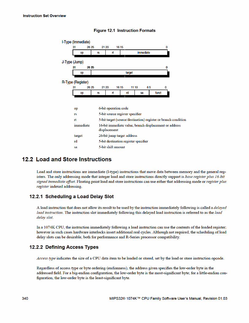

12.3 Computational Instructions
MIPS32® 1074K™ CPU Family Software User’s Manual, Revision 01.03 341
The access type, together with the three low-order bits of the address, defines the bytes accessed within the addressedword, as shown in Table 12.1. Only the combinations shown in Table 12.1 are permissible; other combinations causeaddress-error exceptions.
Instruction fetches are either halfword accesses (MIPS16e™ code) or word accesses (32b code). These referenceswill be impacted by endianness in the same way as load/store references of those sizes.
12.3 Computational Instructions
Computational instructions can be either in register (R-type) format, in which both operands are registers, or in imme-diate (I-type) format, in which one operand is a 16-bit immediate.
Table 12.1 Byte Access Within a Doubleword
Access Type
Low-OrderAddress Bits
Bytes Accessed
Big Endian(63----------------31-------------------0)
Little Endian(63----------------31-------------------0)
2 1 0 Byte Byte
Doubleword 0 0 0 0 1 2 3 4 5 6 7 7 6 5 4 3 2 1 0
Word 0 0 0 0 1 2 3 3 2 1 0
1 0 0 4 5 6 7 7 6 5 4
Triplebyte 0 0 0 0 1 2 2 1 0
0 0 1 1 2 3 3 2 1
1 0 0 4 5 6 6 5 4
1 0 1 5 6 7 7 6 5
Halfword 0 0 0 0 1 1 0
0 1 0 2 3 3 2
1 0 0 4 5 5 4
1 1 0 6 7 7 6
Byte 0 0 0 0 0
0 0 1 1 1
0 1 0 2 2
0 1 1 3 3
1 0 0 4 4
1 0 1 5 5
1 1 0 6 6
1 1 1 7 7

Instruction Set Overview
342 MIPS32® 1074K™ CPU Family Software User’s Manual, Revision 01.03
Computational instructions perform the following operations on register values:
– Arithmetic
– Logical
– Shift
– Count Leading Zeros/Ones
– Multiply
– Divide
These operations fit in the following four categories of computational instructions:
– ALU Immediate instructions
– Three-operand Register-type Instructions
– Shift Instructions
– Multiply And Divide Instructions
12.3.1 Cycle Timing for Multiply and Divide Instructions
Multiply instruction in the integer pipeline are transferred to the multiplier while remaining instructions continuethrough the pipeline; the product of the multiply instruction is saved in the HI and LO registers. If the multiplyinstruction is followed by an MFHI or MFLO before the product is available, the pipeline interlocks until this productdoes become available. Refer to Chapter 2, “Pipeline of the 1074K™ CPU” for more information on instructionlatency and repeat rates.
12.4 Jump and Branch Instructions
Jump and branch instructions change the control flow of a program. All jump and branch instructions occur with adelay of one instruction: that is, the instruction immediately following the jump or branch (the instruction in the so-called delay slot) always executes while the target instruction is being fetched from storage.
12.4.1 Overview of Jump Instructions
Subroutine calls in high-level languages are usually implemented with Jump or Jump and Link instructions, both ofwhich are J-type instructions. In J-type format, the 26-bit target address shifts left 2 bits and combines with the high-order 4 bits of the current program counter to form an absolute address.
Returns, dispatches, and large cross-page jumps are usually implemented with the Jump Register or Jump and LinkRegister instructions. Both are R-type instructions that use the 32-bit byte address contained in one of the general pur-pose registers.
For more information about jump instructions, refer to the individual instructions in MIPS32® Architecture ReferenceManual, Volume II: The MIPS32® Instruction Set.

12.5 Control Instructions
MIPS32® 1074K™ CPU Family Software User’s Manual, Revision 01.03 343
12.4.2 Overview of Branch Instructions
All branch instruction target addresses are computed by adding the address of the instruction in the delay slot to the16-bit offset (shifted left 2 bits and sign-extended to 32 bits). All branches occur with a delay of one instruction.
If a conditional branch likely is not taken, the instruction in the delay slot is nullified.
Branches, jumps, ERET, and DERET instructions should not be placed in the delay slot of a branch or jump.
12.5 Control Instructions
Control instructions allow the software to initiate traps; they are always R-type.
12.6 Coprocessor Instructions
CP0 instructions perform operations on the System Control Coprocessor registers to manipulate the memory manage-ment and exception handling facilities of the processor. Refer to Chapter 13, “1074K™ CPU Instructions” for a list-ing of CP0 instructions.

Instruction Set Overview
344 MIPS32® 1074K™ CPU Family Software User’s Manual, Revision 01.03

Chapter 13
MIPS32® 1074K™ CPU Family Software User’s Manual, Revision 01.03 345
1074K™ CPU Instructions
This chapter supplements the MIPS32® Architecture Reference Manual by describing instruction behavior that isspecific to the 1074K CPU. The chapter contains the following sections:
• Section 13.1 “Understanding the Instruction Descriptions”
• Section 13.2 “1074K™ Opcode Map”
• Section 13.3 “Floating Point Unit Instruction Format Encodings”
• Section 13.4 “MIPS32™ Instruction Set for the 1074K™ CPU”
The 1074K CPU also supports the instructions in the MIPS DSP ASE Revision 2 and the MIPS16e ASE. The MIPSDSP ASE Revision 2 instruction set is described in Chapter 4, “The MIPS® DSP Application-Specific Extension tothe MIPS32® Instruction Set”. The MIPS16e ASE instruction set is described in Chapter 14, “MIPS16e™Application-Specific Extension to the MIPS32® Instruction Set”.
13.1 Understanding the Instruction Descriptions
Refer to Volume II of the MIPS32® Architecture Reference Manual for more information about the instructiondescriptions. That document contains a description of the instruction fields, a definition of terms, and a descriptionfunction notation.
13.2 1074K™ Opcode Map
Table 13.1 Symbols Used in the Instruction Encoding Tables
Symbol Meaning
∗ Operation or field codes marked with this symbol are reserved for future use, are valid encodingsfor a higher-order MIPS ISA level, or are part of an application specific extension not implementedon this CPU. Executing such an instruction will cause a Reserved Instruction Exception.
δ (Also italic field name.) Operation or field codes marked with this symbol are a field class. Theinstruction word must be further decoded by examining additional tables that show values foranother instruction field.
∇ Operation or field codes marked with this symbol represent instructions which are only legal if 64-bit floating point operations are enabled. In other cases, executing such an instruction will cause aReserved Instruction Exception (non-coprocessor encodings or coprocessor instruction encodingsfor a coprocessor to which access is allowed) or a Coprocessor Unusable Exception (coprocessorinstruction encodings for a coprocessor to which access is not allowed).
φ Operation or field codes marked with this symbol are obsolete and will be removed from a futurerevision of the MIPS32 ISA. Software should avoid using these operation or field codes.
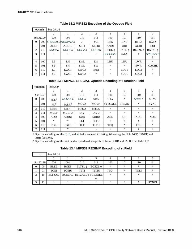
1074K™ CPU Instructions
346 MIPS32® 1074K™ CPU Family Software User’s Manual, Revision 01.03
Table 13.2 MIPS32 Encoding of the Opcode Field
opcode bits 28..26
0 1 2 3 4 5 6 7
bits 31..29 000 001 010 011 100 101 110 111
0 000 SPECIAL δREGIMM δ J JAL BEQ BNE BLEZ BGTZ
1 001 ADDI ADDIU SLTI SLTIU ANDI ORI XORI LUI
2 010 COP0 δ COP1 δ COP2 δ COP1X BEQL φ BNEL φ BLEZL φ BGTZL φ3 011 ∗ ∗ ∗ ∗ SPECIAL2
δJALX ∗ SPECIAL3
δ4 100 LB LH LWL LW LBU LHU LWR ∗5 101 SB SH SWL SW ∗ ∗ SWR CACHE
6 110 LL LWC1 LWC2 PREF ∗ LDC1 LDC2 ∗7 111 SC SWC1 SWC2 * ∗ SDC1 SDC2 ∗
Table 13.3 MIPS32 SPECIAL Opcode Encoding of Function Field
function bits 2..0
0 1 2 3 4 5 6 7
bits 5..3 000 001 010 011 100 101 110 111
0 000 SLL1 MOVCI δ SRL δ SRA SLLV * SRLV δ SRAV
1 001 JR2 JALR2 MOVZ MOVN SYSCALL BREAK * SYNC
2 010 MFHI MTHI MFLO MTLO ∗ * ∗ ∗3 011 MULT MULTU DIV DIVU ∗ ∗ ∗ ∗4 100 ADD ADDU SUB SUBU AND OR XOR NOR
5 101 * * SLT SLTU ∗ ∗ ∗ ∗6 110 TGE TGEU TLT TLTU TEQ * TNE *
7 111 ∗ * ∗ ∗ ∗ * ∗ ∗
1. Specific encodings of the rt, rd, and sa fields are used to distinguish among the SLL, NOP, SSNOP, andEHB functions.
2. Specific encodings of the hint field are used to distinguish JR from JR.HB and JALR from JALR.HB
Table 13.4 MIPS32 REGIMM Encoding of rt Field
rt bits 18..16
0 1 2 3 4 5 6 7
bits 20..19 000 001 010 011 100 101 110 111
0 00 BLTZ BGEZ BLTZL φ BGEZL φ * * * *
1 01 TGEI TGEIU TLTI TLTIU TEQI * TNEI *
2 10 BLTZAL BGEZAL BLTZALLφ BGEZALLφ
* * * *
3 11 * * * * * * * SYNCI

13.2 1074K™ Opcode Map
MIPS32® 1074K™ CPU Family Software User’s Manual, Revision 01.03 347
Table 13.5 MIPS32 SPECIAL2 Encoding of Function Field
function bits 2..0
0 1 2 3 4 5 6 7
bits 5..3 000 001 010 011 100 101 110 111
0 000 MADD MADDU MUL ∗ MSUB MSUBU * *
1 001 * * * * * * * *
2 010 CorExtend
3 011
4 100 CLZ CLO * * ∗ ∗ * *
5 101 * * * * * * * *
6 110 * * * * * * * *
7 111 * * * * * * * SDBBP
Table 13.6 MIPS32 Special3 Encoding of Function Field for Release 2 of the Architecture
function bits 2..0
0 1 2 3 4 5 6 7
bits 5..3 000 001 010 011 100 101 110 111
0 000 EXT ∗ ∗ ∗ INS ∗ ∗ ∗1 001 * * * * * * * *
2 010 * * * * * * * *
3 011 * * * * * * * *
4 100 BSHFL δ * * * ∗ * * *
5 101 * * * * * * * *
6 110 * * * * * * * *
7 111 * * * RDHWR * * * *
Table 13.7 MIPS32 MOVCI Encoding of tf Bit
tf bit 16
0 1
MOVF MOVT
Table 13.8 MIPS32 SRL Encoding of Shift/Rotate
tf bit 21
0 1
SRL ROTR
Table 13.9 MIPS32 SRLV Encoding of Shift/Rotate
tf bit 6
0 1
SRLV ROTRV

1074K™ CPU Instructions
348 MIPS32® 1074K™ CPU Family Software User’s Manual, Revision 01.03
Table 13.10 MIPS32 BSHFLEncoding of sa Field1
sa bits 8..6
0 1 2 3 4 5 6 7
bits 10..9 000 001 010 011 100 101 110 111
0 00 WSBH
1 01
2 10 SEB
3 11 SEH
1. The sa field is sparsely decoded to identify the final instructions. Entries in this table with no mnemonic arereserved for future use by MIPS Technologies and may or may not cause a Reserved Instruction exception.
Table 13.11 MIPS32 COP0 Encoding of rs Field
rs bits 23..21
0 1 2 3 4 5 6 7
bits 25..24 000 001 010 011 100 101 110 111
0 00 MFC0 ∗ * * MTC0 ∗ * *
1 01 * * RDPGPR MFMC01 δ * * WRPGPR *
2 10 C0 δ3 11
1. Release 2 of the Architecture added the MFMC0 function, which is further decoded as the DI and EIinstructions.
Table 13.12 MIPS32COP0 Encoding of Function Field When rs=CO
function bits 2..0
0 1 2 3 4 5 6 7
bits 5..3 000 001 010 011 100 101 110 111
0 000 * TLBR TLBWI * * * TLBWR *
1 001 TLBP * * * * * * *
2 010 * * * * * * * *
3 011 ERET * * * * * * DERET
4 100 WAIT * * * * * * *
5 101 * * * * * * * *
6 110 * * * * * * * *
7 111 * * * * * * * *
Table 13.13 MIPS32 COP1 Encoding of rs Field
rs bits 23..21
0 1 2 3 4 5 6 7
bits 25..24 000 001 010 011 100 101 110 111
0 00 MFC1 ∗ CFC1 MFHC1 MTC1 ∗ CTC1 MTHC1
1 01 BC1 δ ∗ ∗ * * * * *
2 10 S δ D δ * * W δ L δ * *
3 11 * * * * * * * *

13.2 1074K™ Opcode Map
MIPS32® 1074K™ CPU Family Software User’s Manual, Revision 01.03 349
Table 13.14 MIPS32 COP1 Encoding of Function Field When rs=S
function bits 2..0
0 1 2 3 4 5 6 7
bits 5..3 000 001 010 011 100 101 110 111
0 000 ADD SUB MUL DIV SQRT ABS MOV NEG
1 001 ROUND.L∇
TRUNC.L∇
CEIL.L ∇ FLOOR.L∇
ROUND.W TRUNC.W CEIL.W FLOOR.W
2 010 * MOVCF δ MOVZ MOVN * RECIP ∇ RSQRT ∇ *
3 011 * * * * ∗ ∗ ∗ ∗4 100 * CVT.D * * CVT.W CVT.L ∇ ∗ *
5 101 * * * * * * * *
6 110 ∗ ∗ ∗ ∗ ∗ ∗ ∗ ∗7 111 ∗ ∗ ∗ ∗ ∗ ∗ ∗ ∗
Table 13.15 MIPS32 COP1 Encoding of Function Field When rs=D
function bits 2..0
0 1 2 3 4 5 6 7
bits 5..3 000 001 010 011 100 101 110 111
0 000 ADD SUB MUL DIV SQRT ABS MOV NEG
1 001 ROUND.L∇
TRUNC.L∇
CEIL.L ∇ FLOOR.L∇
ROUND.W TRUNC.W CEIL.W FLOOR.W
2 010 * MOVCF δ MOVZ MOVN * RECIP ∇ RSQRT ∇ *
3 011 * * * * ∗ ∗ ∗ ∗4 100 CVT.S * * * CVT.W CVT.L ∇ * *
5 101 * * * * * * * *
6 110 ∗ ∗ ∗ ∗ ∗ ∗ ∗ ∗7 111 ∗ ∗ ∗ ∗ ∗ ∗ ∗ ∗
Table 13.16 MIPS32 COP1 Encoding of Function Field When rs=W or L1
function bits 2..0
0 1 2 3 4 5 6 7
bits 5..3 000 001 010 011 100 101 110 111
0 000 * * * * * * * *
1 001 * * * * * * * *
2 010 * * * * * * * *
3 011 * * * * * * * *
4 100 CVT.S CVT.D * * * * ∗ *
5 101 * * * * * * * *
6 110 * * * * * * * *
7 111 * * * * * * * *
1. Format type L is legal only if 64-bit floating point operations are enabled.
Table 13.17 MIPS32 COP1 Encoding of tf Bit When rs=S or D, Function=MOVCF
tf bit 16
0 1
MOVF fmt MOVT.fmt
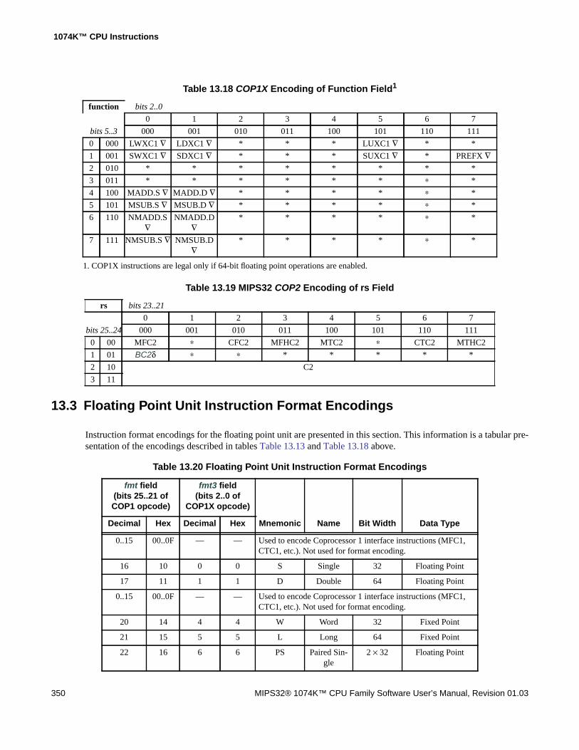
1074K™ CPU Instructions
350 MIPS32® 1074K™ CPU Family Software User’s Manual, Revision 01.03
13.3 Floating Point Unit Instruction Format Encodings
Instruction format encodings for the floating point unit are presented in this section. This information is a tabular pre-sentation of the encodings described in tables Table 13.13 and Table 13.18 above.
Table 13.18 COP1X Encoding of Function Field1
1. COP1X instructions are legal only if 64-bit floating point operations are enabled.
function bits 2..0
0 1 2 3 4 5 6 7
bits 5..3 000 001 010 011 100 101 110 111
0 000 LWXC1 ∇ LDXC1 ∇ * * * LUXC1 ∇ * *
1 001 SWXC1 ∇ SDXC1 ∇ * * * SUXC1 ∇ * PREFX ∇2 010 * * * * * * * *
3 011 * * * * * * ∗ *
4 100 MADD.S ∇ MADD.D ∇ * * * * ∗ *
5 101 MSUB.S ∇ MSUB.D ∇ * * * * ∗ *
6 110 NMADD.S∇
NMADD.D∇
* * * * ∗ *
7 111 NMSUB.S ∇ NMSUB.D∇
* * * * ∗ *
Table 13.19 MIPS32 COP2 Encoding of rs Field
rs bits 23..21
0 1 2 3 4 5 6 7
bits 25..24 000 001 010 011 100 101 110 111
0 00 MFC2 ∗ CFC2 MFHC2 MTC2 ∗ CTC2 MTHC2
1 01 BC2δ ∗ ∗ * * * * *
2 10 C2
3 11
Table 13.20 Floating Point Unit Instruction Format Encodings
fmt field(bits 25..21 ofCOP1 opcode)
fmt3 field(bits 2..0 of
COP1X opcode)
Mnemonic Name Bit Width Data TypeDecimal Hex Decimal Hex
0..15 00..0F — — Used to encode Coprocessor 1 interface instructions (MFC1,CTC1, etc.). Not used for format encoding.
16 10 0 0 S Single 32 Floating Point
17 11 1 1 D Double 64 Floating Point
0..15 00..0F — — Used to encode Coprocessor 1 interface instructions (MFC1,CTC1, etc.). Not used for format encoding.
20 14 4 4 W Word 32 Fixed Point
21 15 5 5 L Long 64 Fixed Point
22 16 6 6 PS Paired Sin-gle
2 × 32 Floating Point
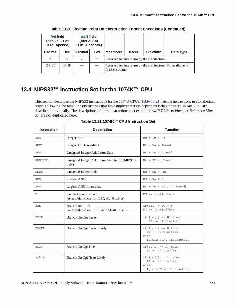
13.4 MIPS32™ Instruction Set for the 1074K™ CPU
MIPS32® 1074K™ CPU Family Software User’s Manual, Revision 01.03 351
13.4 MIPS32™ Instruction Set for the 1074K™ CPU
This section describes the MIPS32 instructions for the 1074K CPUs. Table 13.21 lists the instructions in alphabeticalorder. Following the table, the instructions that have implementation-dependent behavior in the 1074K CPU aredescribed individually. The descriptions of other instructions that exist in theMIPS32® Architecture Reference Man-ual are not duplicated here.
23 17 7 7 Reserved for future use by the architecture.
24..31 18..1F — — Reserved for future use by the architecture. Not available forfmt3 encoding.
Table 13.21 1074K™ CPU Instruction Set
Instruction Description Function
ADD Integer Add Rd = Rs + Rt
ADDI Integer Add Immediate Rt = Rs + Immed
ADDIU Unsigned Integer Add Immediate Rt = Rs +U Immed
ADDIUPC Unsigned Integer Add Immediate to PC (MIPS16only)
Rt = PC +u Immed
ADDU Unsigned Integer Add Rd = Rs +U Rt
AND Logical AND Rd = Rs & Rt
ANDI Logical AND Immediate Rt = Rs & (016 || Immed)
B Unconditional Branch(Assembler idiom for: BEQ r0, r0, offset)
PC += (int)offset
BAL Branch and Link(Assembler idiom for: BGEZAL r0, offset)
GPR[31] = PC + 8PC += (int)offset
BC2F Branch On Cp2 False if (cc[i] == 0) then PC += (int)offset
BC2FL Branch On Cp2 False Likely if (cc[i] == 0)thenPC += (int)offset
elseIgnore Next Instruction
BC2T Branch On Cp2True if(cc[i] == 1) thenPC += (int)offset
BC2TL Branch On Cp2 True Likely if (cc[i] == 1) thenPC += (int)offset
elseIgnore Next Instruction
Table 13.20 Floating Point Unit Instruction Format Encodings (Continued)
fmt field(bits 25..21 ofCOP1 opcode)
fmt3 field(bits 2..0 of
COP1X opcode)
Mnemonic Name Bit Width Data TypeDecimal Hex Decimal Hex

1074K™ CPU Instructions
352 MIPS32® 1074K™ CPU Family Software User’s Manual, Revision 01.03
BEQ Branch On Equal if Rs == RtPC += (int)offset
BEQL Branch On Equal Likely if Rs == RtPC += (int)offset
elseIgnore Next Instruction
BGEZ Branch on Greater Than or Equal To Zero if !Rs[31]PC += (int)offset
BGEZAL Branch on Greater Than or Equal To Zero And Link GPR[31] = PC + 8if !Rs[31]
PC += (int)offset
BGEZALL Branch on Greater Than or Equal To Zero And LinkLikely
GPR[31] = PC + 8if !Rs[31]
PC += (int)offsetelse
Ignore Next Instruction
BGEZL Branch on Greater Than or Equal To Zero Likely if !Rs[31]PC += (int)offset
elseIgnore Next Instruction
BGTZ Branch on Greater Than Zero if !Rs[31] && Rs != 0PC += (int)offset
BGTZL Branch on Greater Than Zero Likely if !Rs[31] && Rs != 0PC += (int)offset
elseIgnore Next Instruction
BLEZ Branch on Less Than or Equal to Zero if Rs[31] || Rs == 0PC += (int)offset
BLEZL Branch on Less Than or Equal to Zero Likely if Rs[31] || Rs == 0PC += (int)offset
elseIgnore Next Instruction
BLTZ Branch on Less Than Zero if Rs[31]PC += (int)offset
BLTZAL Branch on Less Than Zero And Link GPR[31] = PC + 8if Rs[31]
PC += (int)offset
BLTZALL Branch on Less Than Zero And Link Likely GPR[31] = PC + 8if Rs[31]
PC += (int)offsetelse
Ignore Next Instruction
BLTZL Branch on Less Than Zero Likely if Rs[31]PC += (int)offset
elseIgnore Next Instruction
BNE Branch on Not Equal if Rs != RtPC += (int)offset
Table 13.21 1074K™ CPU Instruction Set (Continued)
Instruction Description Function
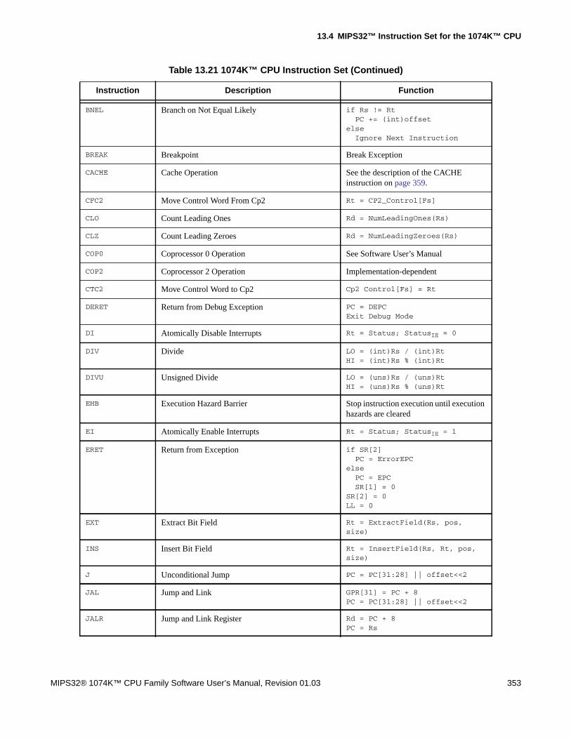
13.4 MIPS32™ Instruction Set for the 1074K™ CPU
MIPS32® 1074K™ CPU Family Software User’s Manual, Revision 01.03 353
BNEL Branch on Not Equal Likely if Rs != RtPC += (int)offset
elseIgnore Next Instruction
BREAK Breakpoint Break Exception
CACHE Cache Operation See the description of the CACHEinstruction on page 359.
CFC2 Move Control Word From Cp2 Rt = CP2_Control[Fs]
CLO Count Leading Ones Rd = NumLeadingOnes(Rs)
CLZ Count Leading Zeroes Rd = NumLeadingZeroes(Rs)
COP0 Coprocessor 0 Operation See Software User’s Manual
COP2 Coprocessor 2 Operation Implementation-dependent
CTC2 Move Control Word to Cp2 Cp2 Control[Fs] = Rt
DERET Return from Debug Exception PC = DEPCExit Debug Mode
DI Atomically Disable Interrupts Rt = Status; StatusIE = 0
DIV Divide LO = (int)Rs / (int)RtHI = (int)Rs % (int)Rt
DIVU Unsigned Divide LO = (uns)Rs / (uns)RtHI = (uns)Rs % (uns)Rt
EHB Execution Hazard Barrier Stop instruction execution until executionhazards are cleared
EI Atomically Enable Interrupts Rt = Status; StatusIE = 1
ERET Return from Exception if SR[2]PC = ErrorEPC
elsePC = EPCSR[1] = 0
SR[2] = 0LL = 0
EXT Extract Bit Field Rt = ExtractField(Rs, pos,size)
INS Insert Bit Field Rt = InsertField(Rs, Rt, pos,size)
J Unconditional Jump PC = PC[31:28] || offset<<2
JAL Jump and Link GPR[31] = PC + 8PC = PC[31:28] || offset<<2
JALR Jump and Link Register Rd = PC + 8PC = Rs
Table 13.21 1074K™ CPU Instruction Set (Continued)
Instruction Description Function

1074K™ CPU Instructions
354 MIPS32® 1074K™ CPU Family Software User’s Manual, Revision 01.03
JALR.HB Jump and Link Register with Hazard Barrier Like JALR, but also clears execution andinstruction hazards
JALRC Jump and Link Register Compact - do not executeinstruction in jump delay slot(MIPS16 only)
Rd = PC + 2PC = Rs
JR Jump Register PC = Rs
JR.HB Jump Register with Hazard Barrier Like JR, but also clears execution andinstruction hazards
JRC Jump Register Compact - do not execute instructionin jump delay slot (MIPS16 only)
PC = Rs
LB Load Byte Rt = (byte)Mem[base+offset]
LBU Unsigned Load Byte Rt = (ubyte)Mem[base+offset]
LDC2 Load Doubleword to Cp2 Ft = memory[base+offset]
LH Load Halfword Rt = (half)Mem[base+offset]
LHU Unsigned Load Halfword Rt = (uhalf)Mem[base+offset]
LL Load Linked Word Rt = Mem[base+offset]LL = 1
See also the description of the LL instruc-tion on page 367.
LUI Load Upper Immediate Rt = immediate << 16
LW Load Word Rt = Mem[Rs+offset]
LWC2 Load Word to Cp2 Ft = memory[base+offset]
LWPC Load Word, PC relative Rt = Mem[PC+offset]
LWL Load Word Left See Architecture Reference Manual
LWR Load Word Right See Architecture Reference Manual
MADD Multiply-Add HI | LO += (int)Rs * (int)Rt
MADDU Multiply-Add Unsigned HI | LO += (uns)Rs * (uns)Rt
MFC0 Move From Coprocessor 0 Rt = CPR[0, Rd, sel]
MFC2 Move From Cp2 Register Rt = Fs31..0
MFHC2 Move From High Half of Cp2 Register Rt = Fs63..32
MFHI Move From HI Rd = HI
MFLO Move From LO Rd = LO
MOVN GPR Conditional Move on Not Zero if Rt ≠ 0 thenRd = Rs
MOVZ GPR Conditional Move on Zero if Rt = 0 thenRd = Rs
Table 13.21 1074K™ CPU Instruction Set (Continued)
Instruction Description Function

13.4 MIPS32™ Instruction Set for the 1074K™ CPU
MIPS32® 1074K™ CPU Family Software User’s Manual, Revision 01.03 355
MSUB Multiply-Subtract HI | LO -= (int)Rs * (int)Rt
MSUBU Multiply-Subtract Unsigned HI | LO -= (uns)Rs * (uns)Rt
MTC0 Move To Coprocessor 0 CPR[0, n, Sel] = Rt
MTC2 Move to Cp2 register Fs = Rt
MTHC2 Move to High Half of Cp2 register Fd = Rt || Fs31..0
MTHI Move To HI HI = Rs
MTLO Move To LO LO = Rs
MUL Multiply with register write HI | LO =UnpredictableRd = ((int)Rs * (int)Rt)31..0
MULT Integer Multiply HI | LO = (int)Rs * (int)Rd
MULTU Unsigned Multiply HI | LO = (uns)Rs * (uns)Rd
NOP No Operation(Assembler idiom for: SLL r0, r0, r0)
NOR Logical NOR Rd = ~(Rs | Rt)
OR Logical OR Rd = Rs | Rt
ORI Logical OR Immediate Rt = Rs | Immed
PREF Prefetch Load Specified Line into Cache. See alsothe description of the PREF instructionon page 369.
RDHWR Read Hardware Register Allows unprivileged access to registersenabled by HWREna register
RDPGPR Read GPR from Previous Shadow Set Rt = SGPR[SRSCtlPSS, Rd]
RESTORE Restore registers and deallocate stack frame(MIPS16 only)
See Architecture Reference Manual
ROTR Rotate Word Right Rd = Rtsa-1..0 || Rt31..sa
ROTRV Rotate Word Right Variable Rd = RtRs-1..0 || Rt31..Rs
SAVE Save registers and allocate stack frame (MIPS16only)
See Architecture Reference Manual
SB Store Byte (byte)Mem[base+offset] = Rt
SC Store Conditional Word if LL = 1 mem[base+offset] = RtRt = LL
See also the description of the SC instruc-tion on page 373.
SDBBP Software Debug Break Point Trap to SW Debug Handler
SDC2 Store Doubleword from Cp2 memory[base+offset] = Ft
Table 13.21 1074K™ CPU Instruction Set (Continued)
Instruction Description Function

1074K™ CPU Instructions
356 MIPS32® 1074K™ CPU Family Software User’s Manual, Revision 01.03
SEB Sign Extend Byte Rd = (byte)Rs
SEH Sign Extend Half Rd = (half)Rs
SH Store Half (half)Mem[base+offset] = Rt
SLL Shift Left Logical Rd = Rt << sa
SLLV Shift Left Logical Variable Rd = Rt << Rs[4:0]
SLT Set on Less Than if (int)Rs < (int)RtRd = 1
elseRd = 0
SLTI Set on Less Than Immediate if (int)Rs < (int)ImmedRt = 1
elseRt = 0
SLTIU Set on Less Than Immediate Unsigned if (uns)Rs < (uns)ImmedRt = 1
elseRt = 0
SLTU Set on Less Than Unsigned if (uns)Rs < (uns)ImmedRd = 1
elseRd = 0
SRA Shift Right Arithmetic Rd = (int)Rt >> sa
SRAV Shift Right Arithmetic Variable Rd = (int)Rt >> Rs[4:0]
SRL Shift Right Logical Rd = (uns)Rt >> sa
SRLV Shift Right Logical Variable Rd = (uns)Rt >> Rs[4:0]
SSNOP Superscalar Inhibit No Operation NOP
SUB Integer Subtract Rt = (int)Rs - (int)Rd
SUBU Unsigned Subtract Rt = (uns)Rs - (uns)Rd
SW Store Word Mem[base+offset] = Rt
SWC2 Store Word From Cp2 Register Mem[base+offset] = Fs
SWL Store Word Left See Architecture Reference Manual
SWR Store Word Right See Architecture Reference Manual
SYNC Synchronize See the description of the SYNC instruc-tion on page 375.
SYNCI Synchronize Caches to Make Instruction WritesEffective
For D-cache writeback and I-cache inval-idate on specified address
SYSCALL System Call SystemCallException
Table 13.21 1074K™ CPU Instruction Set (Continued)
Instruction Description Function

13.4 MIPS32™ Instruction Set for the 1074K™ CPU
MIPS32® 1074K™ CPU Family Software User’s Manual, Revision 01.03 357
TEQ Trap if Equal if Rs == RtTrapException
TEQI Trap if Equal Immediate if Rs == (int)Immed TrapException
TGE Trap if Greater Than or Equal if (int)Rs >= (int)Rt TrapException
TGEI Trap if Greater Than or Equal Immediate if (int)Rs >= (int)Immed TrapException
TGEIU Trap if Greater Than or Equal Immediate Unsigned if (uns)Rs >= (uns)Immed TrapException
TGEU Trap if Greater Than or Equal Unsigned if (uns)Rs >= (uns)Rt TrapException
TLBWI Write Indexed TLB Entry See the description of the TLBWIinstruction on page 381.
TLBWR Write Random TLB Entry See the description of the TLBWRinstruction on page 385.
TLBP Probe TLB for Matching Entry See Software Users Manual
TLBR Read Index for TLB Entry See the description of the TLBR instruc-tion on page 379.
TLT Trap if Less Than if (int)Rs < (int)Rt TrapException
TLTI Trap if Less Than Immediate if (int)Rs < (int)Immed TrapException
TLTIU Trap if Less Than Immediate Unsigned if (uns)Rs < (uns)Immed TrapException
TLTU Trap if Less Than Unsigned if (uns)Rs < (uns)Rt TrapException
TNE Trap if Not Equal if Rs != Rt TrapException
TNEI Trap if Not Equal Immediate if Rs != (int)Immed TrapException
WAIT Wait for Interrupts Stall until interrupt occurs. See thedescription of the WAIT instruction onpage 383.
WRPGPR Write to GPR in Previous Shadow Set SGPR[SRSCtlPSS, Rd] = Rt
WSBH Word Swap Bytes Within HalfWords Rd = Rt23..16 || Rt31..24 || Rt7..0|| Rt15..8
XOR Exclusive OR Rd = Rs ^ Rt
XORI Exclusive OR Immediate Rt = Rs ^ (uns)Immed
ZEB Zero extend byte (MIPS16 only) Rt = (ubyte) Rs
Table 13.21 1074K™ CPU Instruction Set (Continued)
Instruction Description Function
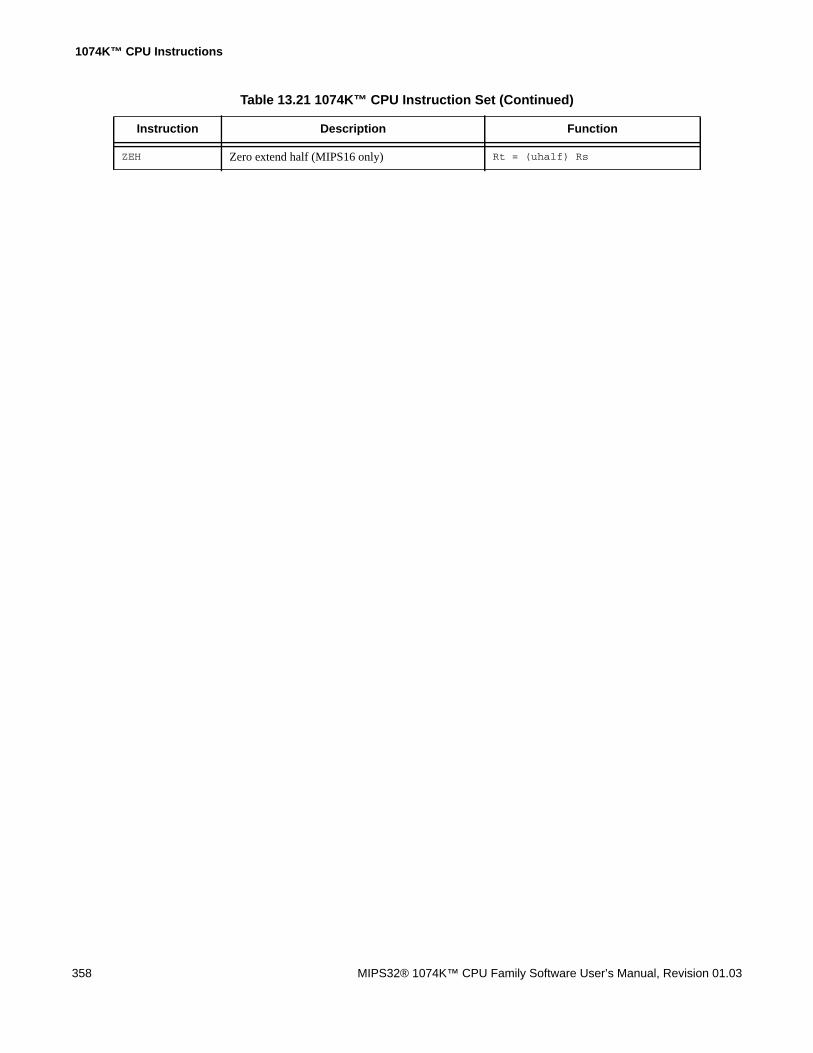
1074K™ CPU Instructions
358 MIPS32® 1074K™ CPU Family Software User’s Manual, Revision 01.03
ZEH Zero extend half (MIPS16 only) Rt = (uhalf) Rs
Table 13.21 1074K™ CPU Instruction Set (Continued)
Instruction Description Function
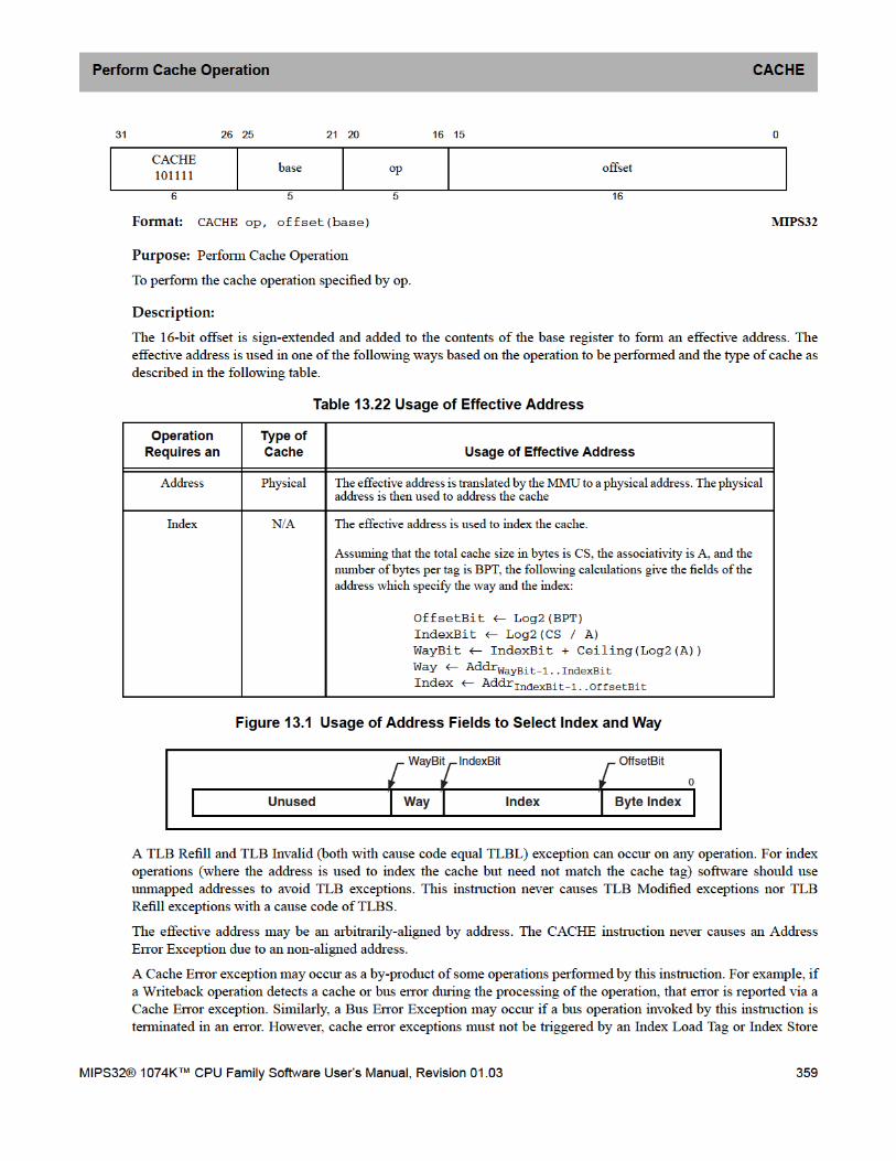

Perform Cache Operation CACHE
360 MIPS32® 1074K™ CPU Family Software User’s Manual, Revision 01.03
tag operation, as these operations are used for initialization and diagnostic purposes.
An address Error Exception (with cause code equal AdEL) occurs if the effective address references a portion of thekernel address space which would normally result in such an exception.
Bits [17:16] of the instruction specify the cache on which to perform the operation, as follows
Some of the operations use coprocessor0 registers as either sources or destinations. Each of the caches has a separateset of Tag and Data registers. The last column in Table 13.23 lists which registers are used by operations to eachcache.
Bits [20:18] of the instruction specify the operation to perform.On Index Load Tag and Index Store Data operations,the specific word (primary D) or double-word (primary I, secondary) that is addressed is loaded into or read from theDDataLo (primary D), L23DataLo, and L23DataHi (secondary), or IDataLo and IDataHi (primary I) registers. Allother cache instructions are line-based, and the word and byte indexes will not affect their operation
Table 13.23 Encoding of Bits[17:16] of CACHE Instruction
Code Name Cache Cop0 Registers Used
2#00 I Primary Instruction ITagLo, ITagHi, IDataLo, IDataHi, ErrCtl
2#01 D Primary Data DTagLo, DTagHi, DDataLo, ErrCtl
2#10 T Tertiary - Not supported
2#11 S Secondary L2TagLo
Table 13.24 Encoding of Bits [20:18] of the CACHE Instruction, ErrCtl[WST, DYT, SPR] Cleared
Code Caches Name
EffectiveAddressOperand
Type Operation
2#000 I Index Invalidate Index Set the state of the cache line at the specifiedindex to invalid.This encoding may be used by software toinvalidate the entire instruction cache by step-ping through all valid indices.
Yes
D, S Index WritebackInvalidate
Index If the state of the cache line at the specifiedindex is valid and dirty, write the line back tothe memory address specified by the cache tag.After that operation is completed, set the stateof the cache line to invalid. If the line is validbut not dirty, set the state of the line to invalid.
This encoding may be used by software toinvalidate the entire data cache by steppingthrough all valid indices. Note that Index StoreTag should be used to initialize the cache atpowerup.
Yes

Perform Cache Operation ICACHE
MIPS32® 1074K™ CPU Family Software User’s Manual, Revision 01.03 361
2#001 I Index Load Tag Index • Read the tag for the cache line at the speci-fied index into the ITagLo and ITagHi regis-ters.
• Read the data corresponding to the dwordin-dex into the IDataLo and IDataHi registers.
• If parity is implemented, read the parity bitscorresponding to the data into ErrCtlPI
Yes
2#001 D Index Load Tag Index • Read the tag for the cache line at the speci-fied index into the DTagLo Coprocessor 0register.
• Read the data corresponding to the wordindex into the DDataLo register.
• Data array parity bits are also read into theErrCtl register.
Yes
2#001 S Index Load Tag Index • Read the tag for the cache line at the speci-fied index into the L23TagLo Coprocessor0 register.
• Read the data corresponding to the dwordindex into the L23DataLo and L23DataHiregisters.
Yes
2#010 I Index Store Tag Index • Write the tag for the cache block at the spec-ified index from the ITagLo and ITagHi reg-isters.
• If parity is implemented, the parity writteninto the cache is generated by the hardwareif ErrCtlPO = 0, or it is obtained from
ITagLo and ITagHi if ErrCtlPO = 1.
Yes
2#010 D,S Index Store Tag Index Write the tag for the cache line at the specifiedindex from the associated TagLo Coprocessor0 register.
By default, the tag parity value will beautomatically calculated. For test purposes, theparity/ECC bits from the associated TagLoregister will be used if ErrCtlPO is set.
This encoding may be used by software to ini-tialize the entire instruction or data caches bystepping through all valid indices. Doing sorequires that the TagLo register associatedwith the cache be initialized first.
Yes
2#011 I Reserved Unspecified Executed as a no-op No
Table 13.24 Encoding of Bits [20:18] of the CACHE Instruction, ErrCtl[WST, DYT, SPR] Cleared (Continued)
Code Caches Name
EffectiveAddressOperand
Type Operation

Perform Cache Operation CACHE
362 MIPS32® 1074K™ CPU Family Software User’s Manual, Revision 01.03
2#011 S Index Store Data Index Write the L23DataHi and L23DataLoCoprocessor 0 register contents at the way anddword index specified.
The ECC bits are always generated by thehardware (if present)
Yes
2#100 All Hit Invalidate Address If the cache line contains the specified address,set the state of the cache line to invalid.This encoding may be used by software toinvalidate a range of addresses from theinstruction cache by stepping through theaddress range by the line size of the cache.
Yes
2#101 I Fill Address Fill the cache from the specified address.
The cache line is refetched even if it is alreadyin the cache. In that case, the existing copy inthe cache is invalidated
Yes
D, S Hit WriteBackInvalidate
Address If the cache line contains the specified addressand it is valid and dirty, write the contents backto memory. After that operation is completed,set the state of the cache line to invalid. If theline is valid but not dirty, set the state of the lineto invalid.
This encoding may be used by software toinvalidate a range of addresses from the datacache by stepping through the address rangeby the line size of the cache.
Yes
2#110 D, S Hit WriteBack Address If the cache line contains the specified addressand it is valid and dirty, write the contents backto memory. After the operation is completed,leave the state of the line valid, but clear thedirty state.
Yes
2#111 All Fetch and Lock Address If the cache does not contain the specifiedaddress, fill it from memory, performing awriteback if required, and set the state to validand locked. If the cache already contains thespecified address, set the state to locked. Theway selected on fill from memory is the leastrecently used.
The lock state is cleared by executing an IndexInvalidate, Index Writeback Invalidate, HitInvalidate, or Hit Writeback Invalidateoperation to the locked line, or via an IndexStore Tag operation with the lock bit reset inthe associated TagLo register.
It is illegal to lock all ways at a given cacheindex. If all ways are locked, subsequentreferences to that index will displace one of thelocked lines.
Yes
Table 13.24 Encoding of Bits [20:18] of the CACHE Instruction, ErrCtl[WST, DYT, SPR] Cleared (Continued)
Code Caches Name
EffectiveAddressOperand
Type Operation

Perform Cache Operation ICACHE
MIPS32® 1074K™ CPU Family Software User’s Manual, Revision 01.03 363
Table 13.25 Encoding of Bits [20:18] of the CACHE Instruction, ErrCtl[WST] Set, ErrCtl[DYT, SPR] Cleared
Code Caches Name
EffectiveAddressOperand
Type Operation
2#001 I Index Load WS Index Read the WS RAM at the specified index intothe ItagLo Coprocessor 0 register. Yes
2#001 D,S Index Load WS Index Read the WS RAM at the specified index intothe associated TagLo Coprocessor 0 register. Yes
2#010 I Index Store WS Index Update the WS RAM at the specified indexfrom the ITagLo Coprocessor 0 register. Yes
2#010 D Index Store WS Index Update the WS RAM at the specified indexfrom the DTagLo Coprocessor 0 register.
Yes
2#010 S Index Store WS Index Update the WS RAM at the specified indexfrom the L23TagLo Coprocessor 0 register.
If ErrCtlPO is set, the dirty parity values in theL23TagLo register will be written to the WSRAM. Otherwise, the parity will be calculatedfor the write data.
Yes
2#011 I Index Store Data Index Write the IDataLo and IDataHi Coprocessor 0register contents at the way and dword indexspecified.
If ErrCtlPO is set, ErrCtlPI is used for the parityvalue. Otherwise, the parity value is calculatedfor the write data.
In addition, the precode value for the write datais also updated in the tag if ErrCtlPCD is notset. If ErrCtlPCO is set, ITagHi is used for theprecode value and its corresponding parity bit.Otherwise, the precode value and itscorresponding parity bit are calculated basedon the write data.
Yes
2#011 D Index Store Data Index Write the DDataLo Coprocessor 0 registercontents at the way and word index specified.
If ErrCtlPO is set, ErrCtlPD is used for theparity value. Otherwise, the parity value iscalculated for the write data.
Yes
2#011 S Index Store ECC Index Write the L23DataLo Coprocessor 0 registercontents to the ECC bits at the way and dwordindex specified.
Yes
All Oth-ers
All Other codes should not be used whileErrCtlWST is set.

Perform Cache Operation CACHE
364 MIPS32® 1074K™ CPU Family Software User’s Manual, Revision 01.03
Note: ErrCtlSPR is a don’t care for cache operations to I-cache.
Note: ErrCtlDYT is a don’t care for cache operations to I-cache.
Restrictions:
The operation of this instruction is UNDEFINED for any operation/cache combination that is not implemented.
The operation of this instruction is UNDEFINED if the operation requires an address, and that address is uncache-able.
If access to Coprocessor 0 is not enabled, a Coprocessor Unusable Exception is signaled.
Operation:
vAddr ← GPR[base] + sign_extend(offset)(pAddr, uncached) ← AddressTranslation(vAddr, DataReadReference)
Table 13.26 Encoding of Bits [20:18] of the CACHE Instruction, ErrCtl[SPR] Set, ErrCtl[DYT, WST] Cleared
Code Caches Name
EffectiveAddressOperand
Type Operation
2#001 D Index Load Tag Index Read the SPRAM tag at the specified index intothe TagLo1 Coprocessor 0 register.
Yes
2#010 D Index Store Tag Index Update the SPRAM tag at the specified indexfrom the TagLo Coprocessor 0 register.
Yes
2#011 D Index Store Data Index Write the DDataLo Coprocessor 0 registercontents into the SPRAM at the word indexspecified.
The data parity is always calculated in thiscase.
Yes
All Oth-ers
D Other codes should not be used whileErrCtlSPR is set.
All S,T Secondary and Tertiary operations should notbe performed while ErrCtlSPR is set.
Table 13.27 Encoding of Bits [20:18] of the CACHE Instruction, ErrCtl[DYT] Set, ErrCtl[SPR, WST] Cleared
Code Caches Name
EffectiveAddressOperand
Type Operation
2#001 D Index Load Tag Index Read the dirty RAM at the specified index intothe TagLo1 Coprocessor 0 register.
Yes
2#010 D Index Store Tag Index Update the dirty RAM at the specified indexfrom the TagLo1 Coprocessor 0 register.
Yes
All Oth-ers
D Other codes should not be used whileErrCtlDYT is set.

Perform Cache Operation ICACHE
MIPS32® 1074K™ CPU Family Software User’s Manual, Revision 01.03 365
CacheOp(op, vAddr, pAddr)
Exceptions:
TLB Refill Exception.
TLB Invalid Exception
Coprocessor Unusable Exception
Programming Notes:
For cache operations that require an index, it is implementation dependent whether the effective address or the trans-lated physical address is used as the cache index. Therefore, the index value should always be converted to a kseg0address by ORing the index with 0x80000000 before being used by the cache instruction. For example, the followingcode sequence performs a data cache Index Store Tag operation using the index passed in GPR a0:
li a1, 0x80000000 /* Base of kseg0 segment */or a0, a0, a1 /* Convert index to kseg0 address */cache DCIndexStTag, 0(a1) /* Perform the index store tag operation */

Perform Cache Operation CACHE
366 MIPS32® 1074K™ CPU Family Software User’s Manual, Revision 01.03

Load Linked Word ILL
MIPS32® 1074K™ CPU Family Software User’s Manual, Revision 01.03 367
Format: LL rt, offset(base) MIPS32
Purpose: Load Linked Word
To load a word from memory for an atomic read-modify-write
Description: GPR[rt] ← memory[GPR[base] + offset]
The LL and SC instructions provide the primitives to implement atomic read-modify-write (RMW) operations forsynchronizable memory locations.
The contents of the 32-bit word at the memory location specified by the aligned effective address are fetched andwritten into GPR rt. The 16-bit signed offset is added to the contents of GPR base to form an effective address.
This begins a RMW sequence on the current processor. There can be only one active RMW sequence per processor.When an LL is executed, it starts an active RMW sequence replacing any other sequence that was active. The RMWsequence is completed by a subsequent SC instruction that either completes the RMW sequence atomically and suc-ceeds, or does not and fails.
Executing LL on one processor does not cause an action that, by itself, causes an SC for the same block to fail onanother processor.
An execution of LL does not have to be followed by execution of SC; a program is free to abandon the RMWsequence without attempting a write.
Restrictions:
The addressed location must be synchronizable by all processors and I/O devices sharing the location; if it is not, theresult is UNPREDICTABLE. Which storage is synchronizable is a function of both CPU and system implementa-tions. See the documentation of the SC instruction for the formal definition.
The effective address must be naturally-aligned. If either of the 2 least-significant bits of the effective address is non-zero, an Address Error exception occurs.
Operation:
vAddr ← sign_extend(offset) + GPR[base]if vAddr1..0 ≠ 02 then
SignalException(AddressError)endif(pAddr, CCA) ← AddressTranslation (vAddr, DATA, LOAD)memword ← LoadMemory (CCA, WORD, pAddr, vAddr, DATA)GPR[rt] ← memwordLLbit ← 1
Exceptions:
TLB Refill, TLB Invalid, Address Error, Reserved Instruction, Watch
Programming Notes:
There is no Load Linked Word Unsigned operation corresponding to Load Word Unsigned.
31 26 25 21 20 16 15 0
LL110000
base rt offset
6 5 5 16

Load Linked Word LL
368 MIPS32® 1074K™ CPU Family Software User’s Manual, Revision 01.03

Prefetch IPREF
MIPS32® 1074K™ CPU Family Software User’s Manual, Revision 01.03 369
Format: PREF hint, offset(base) MIPS32
Purpose: Prefetch
To move data between memory and cache
Description: prefetch_memory(GPR[base] + offset)
PREF adds the 16-bit signed offset to the contents of GPR base to form an effective byte address. The hint field sup-plies information about the way that the data is expected to be used.
PREF does not cause addressing-related exceptions, including TLB exceptions. If the address specified would causean addressing exception, the exception condition is ignored and no data movement occurs. However, even if no data ismoved, some action that is not architecturally visible, such as writeback of a dirty cache line, can take place.
It is implementation-dependent whether a Bus Error or Cache Error exception is reported, if such an error is detectedas a by-product of the action taken by the PREF instruction.
PREF neither generates a memory operation nor modifies the state of a cache line for a location with an uncachedmemory access type, whether this type is specified by the address segment (e.g., kseg1), the programmed coherencyattribute of a segment (e.g., the use of the K0, KU, or K23 fields in the Config register), or the per-page coherencyattribute provided by the TLB.
If PREF results in a memory operation, the memory access type and coherency attribute used for the operation aredetermined by the memory access type and coherency attribute of the effective address, just as it would be if thememory operation had been caused by a load or store to the effective address.
31 26 25 21 20 16 15 0
PREF110011
base hint offset
6 5 5 16
Table 13.28 Values of hint Field for PREF Instruction
Value Name Data Use and Desired Prefetch Action
0 load Use: Prefetched data is expected to be read (not modified).Action: Fetch data as if for a load.
1 store Use: Prefetched data is expected to be stored or modified.Action: Fetch data as if for a store.
2-3 Reserved Reserved - treated as a NOP.
4 load_streamed Use: Prefetched data is expected to be read (not modified) but not reusedextensively; it “streams” through cache.Action: Fetch data as if for a load. LRU replacement information is ignoredand data is placed in way 0 of the cache, so it will be displaced by otherstreamed prefetches and not displace retained prefetches. If way 0 is locked,data will be placed in the way pointed to by the LRU.

Prefetch PREF
370 MIPS32® 1074K™ CPU Family Software User’s Manual, Revision 01.03
Restrictions:
None
Operation:
vAddr ← GPR[base] + sign_extend(offset)(pAddr, CCA) ← AddressTranslation(vAddr, DATA, LOAD)Prefetch(CCA, pAddr, vAddr, DATA, hint)
5 store_streamed Use: Prefetched data is expected to be stored or modified but not reusedextensively; it “streams” through cache.Action: Fetch data as if for a store. LRU replacement information is ignoredand data is placed in way 0 of the cache, so it will be displaced by otherstreamed prefetches and not displace retained prefetches. If way 0 is locked,data will be placed in the way pointed to by the LRU.
6 load_retained Use: Prefetched data is expected to be read (not modified) and reused exten-sively; it should be “retained” in the cache.Action: Fetch data as if for a load. LRU replacement information is used, butway 0 of the cache is specifically excluded. This prevents streamedprefetches from displacing the line.
7 store_retained Use: Prefetched data is expected to be stored or modified and reused exten-sively; it should be “retained” in the cache.Action: Fetch data as if for a store. LRU replacement information is used, butway 0 of the cache is specifically excluded. This prevents streamedprefetches from displacing the line.
8-24 Reserved Reserved - treated as a NOP.
25 writeback_invalidate (alsoknown as “nudge”)
Action: Schedule a writeback of any dirty data. The cache line is marked asinvalid upon completion of the writeback. If cache line is locked, no action istaken. If a line is clean, it will be marked invalid and there will be no write-back scheduled.
26-29 Reserved Reserved - treated as a NOP.
30 PrepareForStore Use: Prepare the cache for writing an entire line, without the overheadinvolved in filling the line from memory.Action: If the reference hits in the cache, no action is taken. If the referencemisses in the cache, a line is selected for replacement, any valid and dirtyvictim is written back to memory, the entire line is filled with zero data, andthe state of the line is marked as valid and dirty.Programming Note: Because the cache line is filled with zero data on a cachemiss, software must not assume that this action, in and of itself, can be usedas a fast bzero-type function.
31 Fast Prepare For Store Use: Prepare the cache for writing an entire line. No data is filled into theline.Action: If reference hits in the cache, no action is taken. If reference missesin the cache, a line is selected for replacement, any valid and dirty victim iswritten back to memory, the line is validated by writing the tag of the linewhile leaving the data as is.Programming Note: If the prefetch is not followed by real writes, it is possi-ble that prevailing data and data parity may indicate a parity error.
Table 13.28 Values of hint Field for PREF Instruction

Prefetch IPREF
MIPS32® 1074K™ CPU Family Software User’s Manual, Revision 01.03 371
Exceptions:
Bus Error, Cache Error
Prefetch does not take any TLB-related or address-related exceptions under any circumstances.
Programming Notes:
Prefetch cannot move data to or from a mapped location unless the translation for that location is present in the TLB.Locations in memory pages that have not been accessed recently may not have translations in the TLB, so prefetchmay not be effective for such locations.
Prefetch does not cause addressing exceptions. A prefetch may be used using an address pointer before the validity ofthe pointer is determined without worrying about an addressing exception.
It is implementation dependent whether a Bus Error or Cache Error exception is reported if such an error is detectedas a by-product of the action taken by the PREF instruction. Typically, this only occurs in systems which have high-reliability requirements.
Prefetch operations have no effect on cache lines that were previously locked with the CACHE instruction.

Prefetch PREF
372 MIPS32® 1074K™ CPU Family Software User’s Manual, Revision 01.03

Store Conditional Word ISC
MIPS32® 1074K™ CPU Family Software User’s Manual, Revision 01.03 373
Format: SC rt, offset(base) MIPS32
Purpose: Store Conditional Word
To store a word to memory to complete an atomic read-modify-write
Description: if atomic_update then memory[GPR[base] + offset] ← GPR[rt], GPR[rt] ← 1else GPR[rt] ← 0
The LL and SC instructions provide primitives to implement atomic read-modify-write (RMW) operations for syn-chronizable memory locations.
The 32-bit word in GPR rt is conditionally stored in memory at the location specified by the aligned effective address.The 16-bit signed offset is added to the contents of GPR base to form an effective address.
The SC completes the RMW sequence begun by the preceding LL instruction executed on the processor. To completethe RMW sequence atomically, the following occur:
• The 32-bit word of GPR rt is stored into memory at the location specified by the aligned effective address.
• A 1, indicating success, is written into GPR rt.
Otherwise, memory is not modified and a 0, indicating failure, is written into GPR rt.
If either ofthe following events occurs between the execution of LL and SC, the SC fails:
• A coherent store is completed by another processor or coherent I/O module into the block of synchronizablephysical memory containing the word. The size and alignment of the block is implementation dependent, but it isat least one word and at most the minimum page size.
• An ERET instruction is executed.
If either of the following events occurs between the execution of LL and SC, the SC may succeed or it may fail; thesuccess or failure is not predictable. Portable programs should not cause one of these events.
• A memory access instruction (load, store, or prefetch) is executed on the processor executing the LL/SC.
• The instructions executed starting with the LL and ending with the SC do not lie in a 2048-byte contiguousregion of virtual memory. (The region does not have to be aligned, other than the alignment required for instruc-tion words.)
The following conditions must be true or the result of the SC is UNPREDICTABLE:
• Execution of SC must have been preceded by execution of an LL instruction.
• An RMW sequence executed without intervening events that would cause the SC to fail must use the sameaddress in the LL and SC. The address is the same if the virtual address, physical address, and cache-coherencealgorithm are identical.
Atomic RMW is provided only for synchronizable memory locations. A synchronizable memory location is one thatis associated with the state and logic necessary to implement the LL/SC semantics. Whether a memory location issynchronizable depends on the processor and system configurations, and on the memory access type used for the
31 26 25 21 20 16 15 0
SC111000
base rt offset
6 5 5 16

Store Conditional Word SC
374 MIPS32® 1074K™ CPU Family Software User’s Manual, Revision 01.03
location:
• Uniprocessor atomicity: To provide atomic RMW on a single processor, all accesses to the location must bemade with memory access type of either cached noncoherent or cached coherent. All accesses must be to one orthe other access type, and they may not be mixed.
• MP atomicity: To provide atomic RMW among multiple processors, all accesses to the location must be madewith a memory access type of cached coherent.
• I/O System: To provide atomic RMW with a coherent I/O system, all accesses to the location must be made witha memory access type of cached coherent. If the I/O system does not use coherent memory operations, thenatomic RMW cannot be provided with respect to the I/O reads and writes.
Restrictions:
The effective address must be naturally-aligned. If either of the 2 least-significant bits of the address is non-zero, anAddress Error exception occurs.
Operation:
vAddr ← sign_extend(offset) + GPR[base]if vAddr1..0 ≠ 02 then
SignalException(AddressError)endif(pAddr, CCA) ← AddressTranslation (vAddr, DATA, STORE)dataword ← GPR[rt]if LLbit then
StoreMemory (CCA, WORD, dataword, pAddr, vAddr, DATA)endifGPR[rt] ← 0 || LLbit
Exceptions:
TLB Refill, TLB Invalid, TLB Modified, Address Error, Watch
Programming Notes:
LL and SC are used to atomically update memory locations, as shown below.
L1:LL T1, (T0) # load counterADDI T2, T1, 1 # incrementSC T2, (T0) # try to store, checking for atomicityBEQ T2, 0, L1 # if not atomic (0), try againNOP # branch-delay slot
Exceptions between the LL and SC cause SC to fail, so persistent exceptions must be avoided. Some examples ofthese are arithmetic operations that trap, system calls, and floating point operations that trap or require software emu-lation assistance.
LL and SC function on a single processor for cached noncoherent memory so that parallel programs can be run onuniprocessor systems that do not support cached coherent memory access types.

Synchronize Shared Memory ISYNC
MIPS32® 1074K™ CPU Family Software User’s Manual, Revision 01.03 375
Format: SYNC (stype = 0 implied) MIPS32
Purpose: Synchronize Shared Memory
To order loads and stores.
Description:
These types of ordering guarantees are available through the SYNC instruction:
• Completion Barriers
• Ordering Barriers
Simple Description of Completion Barrier:
• SYNC affects only uncached and cached coherent loads and stores. The loads and stores that occur before theSYNC must be completed before the loads and stores after the SYNC are allowed to start.
• Loads are completed when the destination register is written. Stores are completed when the stored value is visi-ble to every other processor in the system.
• SYNC is required, potentially in conjunction with SSNOP (in Release 1 of the Architecture) or EHB (in Release2 of the Architecture), to guarantee that memory reference results are visible across operating mode changes. Forexample, a SYNC is required on entry to and exit from Debug Mode to guarantee that memory affects are han-dled correctly.
Detailed Description of Completion Barrier:
• SYNC does not guarantee the order in which instruction fetches are performed. A stype value of zero will alwaysbe defined such that it performs the most complete set of synchronization operations that are defined. This meansstype zero always does a completion barrier that affects both loads and stores preceding the SYNC instructionand both loads and stores that are subsequent to the SYNC instruction. Non-zero values of stype may be definedby the architecture or specific implementations to perform synchronization behaviors that are less complete thanthat of stype zero. If an implementation does not use one of these non-zero values to define a different synchroni-zation behavior, then that non-zero value of stype must act the same as stype zero completion barrier. This allowssoftware written for an implementation with a lighter-weight barrier to work on another implementation whichonly implements the stype zero completion barrier.
All completion barrier types will flush any pending writes and potentially generate an external SYNC request. Anexternal SYNC request will be sent if Config7ES = 1 and SI_SyncTxEn = 1. The first term is a software enable forexternalizing SYNCs and the second term is a hardware enable, indicating that the next level device (L2 or system)supports SYNC transactions. The CPU will wait for all pending reads to complete as well as the SYNC response if itwas externalized.
• 0x2 - Implementation specific stype. Intervention SYNC. When coherence is enabled, this SYNC will generate aCoherentSync request. The Coherence Manager will respond to the SYNC when the interventions for all oldercoherent requests have been completed. If coherence is not enabled, will default to stype 0x0.
31 26 25 21 20 16 15 11 10 6 5 0
SPECIAL000000
000 0000 0000 0000 0
stypeSYNC001111
6 15 5 6
Synchronize Shared Memory ISYNC
376 MIPS32® 1074K™ CPU Family Software User’s Manual, Revision 01.03
• 0x3 - Implementation specific stype. Memory SYNC. When coherence is enabled, this SYNC will also generatea CoherentSync request. When interventions for all older coherent requests have completed, the sync will be sentto memory interface unit. All pending transactions will be sent out. If the next level device (L2 or system) sup-ports legacy SYNC transactions, as indicated by SI_CM_SyncTxEn = 1, and CM_SYNC_TX_DISABLE inthe CM Control GCR is 0, an external SYNC request will also be generated. The CM will send a response to theCPU when all prior requests have completed and a SYNC response is received (if it was externalized). If coher-ence is not enabled, will default to stype 0x0.
• 0x0 - If coherence is enabled, this will be mapped to either a type 0x2 or 0x3 based on the value of the SYNC-CTL bit in the CM Control GCR. If coherence is not enabled, a legacy SYNC request will be generated. This willbypass the intervention pipeline in the CM and go directly to the memory unit. If SyncTxEn = 1 andCM_SYNC_TX_DISABLE in the CM Control GCR is 0, an external SYNC request will be generated.
Simple Description of Ordering Barrier:
• The specified memory instructions (loads or stores or both) that occur before the SYNC instruction mustalways be ordered before the specified memory instructions after the SYNC.
• Memory instructions which are ordered before other memory instructions are processed by the load/storedatapath first before the other memory instructions.
Detailed Description of Ordering Barrier:
• Every synchronizable specified memory instruction (loads or stores or both) that occurs in the instructionstream before the SYNC instruction must reach a stage in the load/store datapath after which no instructionre-ordering is possible before any synchronizable specified memory instruction which occurs after theSYNC instruction in the instruction stream reaches the same stage in the load/store datapath.
• If any memory instruction before the SYNC instruction in program order, generates a memory request to theexternal memory and any memory instruction after the SYNC instruction in program order also generates amemory request to external memory, the memory request belonging to the older instruction must be globallyperformed before the time the memory request belonging to the younger instruction is globally performed.
• The barrier does not guarantee the order in which instruction fetches are performed.
As compared to the completion barrier, the ordering barrier is a lighter-weight operation as it does not require thespecified instructions before the SYNC to be already completed. Instead it only requires that those specified instruc-tions which are subsequent to the SYNC in the instruction stream are never re-ordered for processing ahead of thespecified instructions which are before the SYNC in the instruction stream. This potentially reduces how many cyclesthe barrier instruction must stall before it completes.
The Acquire and Release barrier types are used to minimize the memory orderings that must be maintained and stillhave software synchronization work.
Because the CPU processes loads and stores in order, ordering barriers are much lighter weight. The LSU does notissue the RMB and Acquire barrier types to the BIU. For the MB, WMB, Release barrier types, the LSU will com-plete any store hits and hit-type cacheops before issuing them to the BIU. The BIU will stop merging on all WBBentries. No external request will be generated and the CPU will not wait for pending transactions to complete.

Synchronize Shared Memory ISYNC
MIPS32® 1074K™ CPU Family Software User’s Manual, Revision 01.03 377
For the purposes of this description, the CACHE, PREF and PREFX instructions are treated as loads and stores. Thatis, these instructions and the memory transactions sourced by these instructions obey the ordering and completionrules of the SYNC instruction.
Table 13.29 lists the available completion barrier and ordering barriers behaviors that can be specified using the stypefield.
Restrictions:
The effect of SYNC on the global order of loads and stores for memory access types other than uncached and cachedcoherent is UNPREDICTABLE.
Operation:
SyncOperation(stype)
Table 13.29 Encodings of the Bits[10:6] of the SYNC instruction; the SType Field
Code Name
Older instructionswhich must reach
the load/storeordering point
before the SYNCinstructioncompletes.
Youngerinstructions
which must reachthe load/storeordering pointonly after the
SYNC instructioncompletes.
Older instructionswhich must be
globallyperformed when
the SYNCinstructioncompletes
0x0 SYNCor
SYNC(0)
Loads, Stores Loads, Stores Loads, Stores
0x2 SYNC(2)Intervention Sync
Load,Stores Load,Stores Load,Stores
0x3 SYNC(3)Memory Sync
Load,Stores Load,Stores Load,Stores
0x4 SYNC_WMBor
SYNC(4)
Stores Stores
0x10 SYNC_MBor
SYNC(16)
Loads, Stores Loads, Stores
0x11 SYNC_ACQUIREor
SYNC(17)
Loads Loads, Stores
0x12 SYNC_RELEASEor
SYNC(18)
Loads, Stores Stores
0x13 SYNC_RMBor
SYNC(19)
Loads Loads
0x1, 0x5-0xF,0x14 -0x1F
RESERVED
Synchronize Shared Memory ISYNC
378 MIPS32® 1074K™ CPU Family Software User’s Manual, Revision 01.03
Exceptions:
None

Read Indexed TLB Entry ITLBR
MIPS32® 1074K™ CPU Family Software User’s Manual, Revision 01.03 379
Format: TLBR MIPS32
Purpose: Read Indexed TLB Entry
To read an entry from the TLB.
Description:
The EntryHi, EntryLo0, EntryLo1, and PageMask registers are loaded with the contents of the TLB entry pointedto by the Index register. In Release 1 of the Architecture, it is implementation dependent whether multiple TLBmatches are detected on a TLBR. However, implementations are strongly encouraged to report multiple TLB matchesonly on a TLB write. In Release 2 of the Architecture, multiple TLB matches may only be reported on a TLB write.Note that the value written to the EntryHi, EntryLo0, and EntryLo1 registers may be different from that originallywritten to the TLB via these registers in that:
• The value returned in the G bit in both the EntryLo0 and EntryLo1 registers comes from the single G bit in theTLB entry. Recall that this bit was set from the logical AND of the two G bits in EntryLo0 and EntryLo1 whenthe TLB was written.
Restrictions:
The operation is UNDEFINED if the contents of the Index register are greater than or equal to the number of TLBentries in the processor.
If access to Coprocessor 0 is not enabled, a Coprocessor Unusable Exception is signaled.
Operation:
i ← Indexif i > (TLBEntries - 1) then
UNDEFINEDendifPageMaskMask ← TLB[i]MaskEntryHi ←
TLB[i]VPN2 ||05 || TLB[i]ASID
EntryLo1 ← 0 ||TLB[i]PFN1 ||TLB[i]C1 || TLB[i]D1 || TLB[i]V1 || TLB[i]G
EntryLo0 ← 0 ||TLB[i]PFN0 ||TLB[i]C0 || TLB[i]D0 || TLB[i]V0 || TLB[i]G
Exceptions:
Coprocessor Unusable
Machine Check
31 26 25 24 6 5 0
COP0010000
CO1
0000 0000 0000 0000 0000
TLBR000001
6 1 19 6

Read Indexed TLB Entry ITLBR
380 MIPS32® 1074K™ CPU Family Software User’s Manual, Revision 01.03

Write Indexed TLB Entry ITLBWI
MIPS32® 1074K™ CPU Family Software User’s Manual, Revision 01.03 381
Format: TLBWI MIPS32
Purpose: Write Indexed TLB Entry
To write a TLB entry indexed by the Index register.
Description:
The TLB entry pointed to by the Index register is written from the contents of the EntryHi, EntryLo0, EntryLo1, andPageMask registers. If multiple TLB matches are detected on a TLBWI, a Machine Check exception is signaled.The information written to the TLB entry may be different from that in the EntryHi, EntryLo0, and EntryLo1 regis-ters, in that:
• The single G bit in the TLB entry is set from the logical AND of the G bits in the EntryLo0 and EntryLo1 regis-ters.
Restrictions:
The operation is UNDEFINED if the contents of the Index register are greater than or equal to the number of TLBentries in the processor.
If access to Coprocessor 0 is not enabled, a Coprocessor Unusable Exception is signaled.
Operation:
i ← IndexTLB[i]Mask ← PageMaskMaskTLB[i]VPN2 ← EntryHiVPN2TLB[i]ASID ← EntryHiASIDTLB[i]G ← EntryLo1G and EntryLo0GTLB[i]PFN1 ← EntryLo1PFNTLB[i]C1 ← EntryLo1CTLB[i]D1 ← EntryLo1DTLB[i]V1 ← EntryLo1VTLB[i]PFN0 ← EntryLo0PFNTLB[i]C0 ← EntryLo0CTLB[i]D0 ← EntryLo0DTLB[i]V0 ← EntryLo0V
Exceptions:
Coprocessor Unusable
Machine Check
31 26 25 24 6 5 0
COP0010000
CO1
0000 0000 0000 0000 0000
TLBWI000010
6 1 19 6

Write Indexed TLB Entry ITLBWI
382 MIPS32® 1074K™ CPU Family Software User’s Manual, Revision 01.03

Enter Standby Mode WAIT
MIPS32® 1074K™ CPU Family Software User’s Manual, Revision 01.03 383
Format: WAIT MIPS32
Purpose: Enter Standby Mode
Wait for Event
Description:
The WAIT instruction forces the CPU into low-power mode. The pipeline is stalled, and when all external requestsare completed, the processor’s main clock is stopped. The processor will restart when reset (SI_Reset orSI_ColdReset) is signaled or when an interrupt is signalled, irrespective of whether the interrupt is enabled or not.(SI_NMI, SI_Int, or EJ_DINT). Note that the CPU does not use the code field in this instruction. If the pipelinerestarts as the result of an interrupt, that interrupt is taken between the WAIT instruction and the following instruction(EPC for the interrupt points to the instruction following the WAIT instruction).
Restrictions:
The operation of the processor is UNDEFINED if a WAIT instruction is placed in the delay slot of a branch or ajump.
If access to Coprocessor 0 is not enabled, a Coprocessor Unusable Exception is signaled.
Operation:
I: Enter lower power modeI+1:/* Potential interrupt taken here */
Exceptions:
Coprocessor Unusable Exception
31 26 25 24 6 5 0
COP0010000
CO1
Implementation-Dependent CodeWAIT
100000
6 1 19 6
Enter Standby Mode WAIT
384 MIPS32® 1074K™ CPU Family Software User’s Manual, Revision 01.03

Write Random TLB Entry TLBWR
MIPS32® 1074K™ CPU Family Software User’s Manual, Revision 01.03 385
Format: TLBWR MIPS32
Purpose: Write Random TLB Entry
To write a TLB entry indexed by the Random register.
Description:
The TLB entry pointed to by the Random register is written from the contents of the EntryHi, EntryLo0, EntryLo1,and PageMask registers. If multiple TLB matches are detected on a TLBWR, a Machine Check exception is sig-naled. The information written to the TLB entry may be different from that in the EntryHi, EntryLo0, and EntryLo1registers, in that:
• The single G bit in the TLB entry is set from the logical AND of the G bits in the EntryLo0 and EntryLo1 regis-ters.
Restrictions:
If access to Coprocessor 0 is not enabled, a Coprocessor Unusable Exception is signaled.
Operation:
i ← RandomTLB[i]Mask ← PageMaskMaskTLB[i]VPN2 ← EntryHiVPN2TLB[i]ASID ← EntryHiASIDTLB[i]G ← EntryLo1G and EntryLo0GTLB[i]PFN1 ← EntryLo1PFNTLB[i]C1 ← EntryLo1CTLB[i]D1 ← EntryLo1DTLB[i]V1 ← EntryLo1VTLB[i]PFN0 ← EntryLo0PFNTLB[i]C0 ← EntryLo0CTLB[i]D0 ← EntryLo0DTLB[i]V0 ← EntryLo0V
Exceptions:
Coprocessor Unusable
Machine Check
31 26 25 24 6 5 0
COP0010000
CO1
0000 0000 0000 0000 0000
TLBWR000110
6 1 19 6

Write Random TLB Entry TLBWR
386 MIPS32® 1074K™ CPU Family Software User’s Manual, Revision 01.03

Chapter 14
MIPS32® 1074K™ CPU Family Software User’s Manual, Revision 01.03 387
MIPS16e™ Application-Specific Extension to the MIPS32®Instruction Set
This chapter describes the MIPS16e™ ASE as implemented in the 1074K CPU. Refer to Volume IV-a of the MIPS32Architecture Reference Manual for a general description of the MIPS16e ASE and detailed descriptions of theinstructions.
This chapter covers the following topics:
• Section 14.1 “Instruction Bit Encoding”
• Section 14.2 “Instruction Listing”
14.1 Instruction Bit Encoding
Table 14.2 through Table 14.9 describe the encoding used for the MIPS16e ASE. Table 14.1 describes the meaning ofthe symbols used in the tables.
Table 14.1 Symbols Used in the Instruction Encoding Tables
∗ Operation or field codes marked with this symbol are reserved for future use. Executing such aninstruction causes a Reserved Instruction Exception.
δ (Also italic field name.) Operation or field codes marked with this symbol denote a field class. Theinstruction word must be further decoded by examining additional tables that show values for anotherinstruction field.
β Operation or field codes marked with this symbol represent a valid encoding for a higher-order MIPSISA level. Executing such an instruction causes a Reserved Instruction Exception.
θ Operation or field codes marked with this symbol are available to licensed MIPS partners. To avoidmultiple conflicting instruction definitions, the partner must notify MIPS Technologies, Inc. when oneof these encodings is used. If no instruction is encoded with this value, executing such an instructionmust cause a Reserved Instruction Exception (SPECIAL2 encodings or coprocessor instruction encod-ings for a coprocessor to which access is allowed) or a Coprocessor Unusable Exception (coprocessorinstruction encodings for a coprocessor to which access is not allowed).
σ Field codes marked with this symbol represent an EJTAG support instruction and implementation ofthis encoding is optional for each implementation. If the encoding is not implemented, executing suchan instruction must cause a Reserved Instruction Exception. If the encoding is implemented, it mustmatch the instruction encoding as shown in the table.
ε Operation or field codes marked with this symbol are reserved for MIPS Application Specific Exten-sions. If the ASE is not implemented, executing such an instruction must cause a Reserved InstructionException.
φ Operation or field codes marked with this symbol are obsolete and will be removed from a future revi-sion of the MIPS64 ISA. Software should avoid using these operation or field codes.
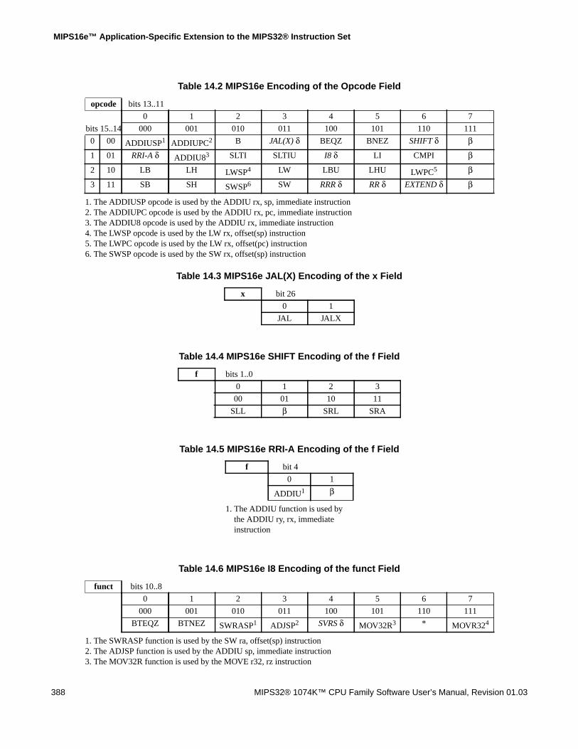
MIPS16e™ Application-Specific Extension to the MIPS32® Instruction Set
388 MIPS32® 1074K™ CPU Family Software User’s Manual, Revision 01.03
Table 14.2 MIPS16e Encoding of the Opcode Field
opcode bits 13..11
0 1 2 3 4 5 6 7
bits 15..14 000 001 010 011 100 101 110 111
0 00 ADDIUSP1
1. The ADDIUSP opcode is used by the ADDIU rx, sp, immediate instruction
ADDIUPC2
2. The ADDIUPC opcode is used by the ADDIU rx, pc, immediate instruction
B JAL(X) δ BEQZ BNEZ SHIFT δ β
1 01 RRI-A δ ADDIU83
3. The ADDIU8 opcode is used by the ADDIU rx, immediate instruction
SLTI SLTIU I8 δ LI CMPI β
2 10 LB LH LWSP4
4. The LWSP opcode is used by the LW rx, offset(sp) instruction
LW LBU LHU LWPC5
5. The LWPC opcode is used by the LW rx, offset(pc) instruction
β
3 11 SB SH SWSP6
6. The SWSP opcode is used by the SW rx, offset(sp) instruction
SW RRR δ RR δ EXTEND δ β
Table 14.3 MIPS16e JAL(X) Encoding of the x Field
x bit 26
0 1
JAL JALX
Table 14.4 MIPS16e SHIFT Encoding of the f Field
f bits 1..0
0 1 2 3
00 01 10 11
SLL β SRL SRA
Table 14.5 MIPS16e RRI-A Encoding of the f Field
f bit 4
0 1
ADDIU1
1. The ADDIU function is used bythe ADDIU ry, rx, immediateinstruction
β
Table 14.6 MIPS16e I8 Encoding of the funct Field
funct bits 10..8
0 1 2 3 4 5 6 7
000 001 010 011 100 101 110 111
BTEQZ BTNEZ SWRASP1
1. The SWRASP function is used by the SW ra, offset(sp) instruction
ADJSP2
2. The ADJSP function is used by the ADDIU sp, immediate instruction
SVRS δ MOV32R3
3. The MOV32R function is used by the MOVE r32, rz instruction
* MOVR324

14.2 Instruction Listing
MIPS32® 1074K™ CPU Family Software User’s Manual, Revision 01.03 389
14.2 Instruction Listing
The MIPS16e instructions are listed by instruction type in Table 14.12 through Table 14.19.
4. The MOVR32 function is used by the MOVE ry, r32 instruction
Table 14.7 MIPS16e RRR Encoding of the f Field
f bits 1..0
0 1 2 3
00 01 10 11
β ADDU β SUBU
Table 14.8 MIPS16e RR Encoding of the Funct Field
funct bits 2..0
0 1 2 3 4 5 6 7
bits 4..3 000 001 010 011 100 101 110 111
0 00 J(AL)R(C) δ SDBBP SLT SLTU SLLV BREAK SRLV SRAV
1 01 β * CMP NEG AND OR XOR NOT
2 10 MFHI CNVT δ MFLO β β * β β3 11 MULT MULTU DIV DIVU β β β β
Table 14.9 MIPS16e I8 Encoding of the s Field when funct=SVRS
s bit 7
0 1
RESTORE SAVE
Table 14.10 MIPS16e RR Encoding of the ry Field when funct=J(AL)R(C)
ry bits 7..5
0 1 2 3 4 5 6 7
000 001 010 011 100 101 110 111
JR rx JR ra JALR * JRC rx JRC ra JALRC *
Table 14.11 MIPS16e RR Encoding of the ry Field when funct=CNVT
ry bits 7..5
0 1 2 3 4 5 6 7
000 001 010 011 100 101 110 111
ZEB ZEH β * SEB SEH β *

MIPS16e™ Application-Specific Extension to the MIPS32® Instruction Set
390 MIPS32® 1074K™ CPU Family Software User’s Manual, Revision 01.03
Table 14.12 MIPS16e Load and Store Instructions
Mnemonic InstructionExtensibleInstruction
LB Load Byte Yes
LBU Load Byte Unsigned Yes
LH Load Halfword Yes
LHU Load Halfword Unsigned Yes
LW Load Word Yes
SB Store Byte Yes
SH Store Halfword Yes
SW Store Word Yes
Table 14.13 MIPS16e Save and Restore Instructions
Mnemonic InstructionExtensibleInstruction
RESTORE Restore Registers and Deallocate Stack Frame Yes
SAVE Save Registers and Setup Stack Frame Yes
Table 14.14 MIPS16e ALU Immediate Instructions
Mnemonic InstructionExtensibleInstruction
ADDIU Add Immediate Unsigned Yes
CMPI Compare Immediate Yes
LI Load Immediate Yes
SLTI Set on Less Than Immediate Yes
SLTIU Set on Less Than Immediate Unsigned Yes
Table 14.15 MIPS16e Arithmetic Two or Three Operand Register Instructions
Mnemonic InstructionExtensibleInstruction
ADDU Add Unsigned No
AND AND No
CMP Compare No
MOVE Move No
NEG Negate No

14.2 Instruction Listing
MIPS32® 1074K™ CPU Family Software User’s Manual, Revision 01.03 391
NOT Not No
OR OR No
SEB Sign-Extend Byte No
SEH Sign-Extend Halfword No
SLT Set on Less Than No
SLTU Set on Less Than Unsigned No
SUBU Subtract Unsigned No
XOR Exclusive OR No
ZEB Zero-Extend Byte No
ZEH Zero-Extend Halfword No
Table 14.16 MIPS16e Special Instructions
Mnemonic InstructionExtensibleInstruction
BREAK Breakpoint No
SDBBP Software Debug Breakpoint No
EXTEND Extend No
Table 14.17 MIPS16e Multiply and Divide Instructions
Mnemonic InstructionExtensibleInstruction
DIV Divide No
DIVU Divide Unsigned No
MFHI Move From HI No
MFLO Move From LO No
MULT Multiply No
MULTU Multiply Unsigned No
Table 14.18 MIPS16e Jump and Branch Instructions
Mnemonic InstructionExtensibleInstruction
B Branch Unconditional Yes
BEQZ Branch on Equal to Zero Yes
BNEZ Branch on Not Equal to Zero Yes
Table 14.15 MIPS16e Arithmetic Two or Three Operand Register Instructions
Mnemonic InstructionExtensibleInstruction

MIPS16e™ Application-Specific Extension to the MIPS32® Instruction Set
392 MIPS32® 1074K™ CPU Family Software User’s Manual, Revision 01.03
BTEQZ Branch on T Equal to Zero Yes
BTNEZ Branch on T Not Equal to Zero Yes
JAL Jump and Link No
JALR Jump and Link Register No
JALRC Jump and Link Register Compact No
JALX Jump and Link Exchange No
JR Jump Register No
JRC Jump Register Compact No
Table 14.19 MIPS16e Shift Instructions
Mnemonic InstructionExtensibleInstruction
SRA Shift Right Arithmetic Yes
SRAV Shift Right Arithmetic Variable No
SLL Shift Left Logical Yes
SLLV Shift Left Logical Variable No
SRL Shift Right Logical Yes
SRLV Shift Right Logical Variable No
Table 14.18 MIPS16e Jump and Branch Instructions
Mnemonic InstructionExtensibleInstruction

Appendix A
MIPS32® 1074K™ CPU Family Software User’s Manual, Revision 01.03 393
References
This appendix lists other publications available from MIPS Technologies, Inc. that are referenced in this document.These documents may be included in the $MIPS_PROJECT/doc area of a typical 1074K soft or hard CPU release,or in some cases may be available on the MIPS web site http://www.mips.com.
1. MIPS32® Architecture For Programmers, Volume I: Introduction to the MIPS32 ArchitectureMIPS document: MD0082
2. MIPS32® Architecture For Programmers, Volume II: The MIPS32 Instruction SetMIPS document: MD0082
3. MIPS32® Architecture For Programmers, Volume IV-e: The MIPS® DSP Application-Specific Extension to theMIPS32 ArchitectureMIPS document: MD00374
4. MIPS32® 1074K™ Coherent Processing System DatasheetMIPS document: MD00745
5. MIPS32® 1074K™ Coherent Processing System User's ManualMIPS document: MD00748
6. MIPS32® 1074K™ CPU Family Integrator’s GuideMIPS document: MD00747
7. MIPS32® 1074K™ CPU Family Implementor’s GuideMIPS document: MD00746
8. Programming the MIPS32® 1074K™ Coherent Processing System FamilyMIPS document: MD00750
9. Programming the MIPS 74KTM Family Cores for DSPMIPS document: MD00544
10. CorExtend™ Instruction Integrator’s Guide for MIPS32® 1074K™ CPUsMIPS document: MD00787
11. Getting Started with CorExtend® Instructions for MIPS32® 1074K™ CPUsMIPS document: MD00788
12. MIPS® EJTAG SpecificationMIPS document: MD00047
13. MIPS® PDtrace™ Interface and Trace Control Block SpecificationMIPS document: MD00439

References
394 MIPS32® 1074K™ CPU Family Software User’s Manual, Revision 01.03
14. PDtrace™ and TCB Usage GuidelinesMIPS document: MD00365
15. MIPS32® Architecture For Programmers, Volume III: Privileged Resource ArchitectureMIPS document: MD00088

Appendix B
MIPS32® 1074K™ CPU Family Software User’s Manual, Revision 01.03 395
Revision History
MIPS documents include change bars (vertical bars in the page margin) that mark significant changes to the docu-ment since its last release. Change bars are removed for changes which are more than one revision old.
This document may refer to Architecture specifications (for example, instruction set descriptions and EJTAG registerdefinitions), and change bars in these sections indicate changes since the previous version of the relevant Architecturedocument.
Date Revision Description
July 30, 2010 01.00 • Initial external release.
September 24, 2010 01.01 • Add description of L1 I-cache support for 0KB sizeand L1 D-cache support for 16KB, 32KB and 64KBsizes.
• Add description of address bits in Index field ofCacheErr register,
March 30, 2011 01.02 • Add description of 6 new bits in DCR.• Add description of 2 new bits in Implementation reg-
ister.• Updated hazard tables.• Updated description of DC bit in Cause register.
June 03, 2011 01.03 • Corrected FIR.ProcessorID information.
Copyright © Wave Computing, Inc. All rights reserved. www.wavecomp.ai