minimizing emi caused by radially propagating waves inside high … · mikrotalasna revija decembar...
TRANSCRIPT
Mikrotalasna revija Decembar 2001.
72
Minimizing EMI Caused by Radially Propagating Waves Inside High Speed Digital Logic PCBs
Franz Gisin, Zorica Pantic-Tanner
Abstract - One of the primary modes of radiation from printed circuit boards (PCBs) are due to emissions along the edges of printed circuit boards. A variety of edge treatment techniques are used to minimize these two effects including adding a string of vias around the periphery of the PCB to short out ground planes (fencing), totally shielding the printed circuit board between two outer ground-planes and edge plating, and pulling back power planes from the edges by a factor of up to 20 times the plane-to-plane separation distance (20H rule) to minimize PCB resonance effects. This paper describes the underlying mechanism of how radiation from PCB edges actually takes place, and then shows how these techniques impact the EMC aspects of printed circuit board edge structures.
Keywords - Printed circuit board, edge effects, via fencing, 20H Rule, radial transmission lines.
I. INTRODUCTION
As clock harmonics of high-speed digital logic based systems such as local area networks and routers routinely exceed 1 GHz, the threat of electromagnetic interference (EMI) to wireless communications services increases significantly. At these frequencies, PCB dimensions become electrically long, and harmonics of digital logic clocks can excite resonances which in turn cause the PCB to become an efficient radiator thereby coupling energy into enclosure cavities and enclosure apertures such as seams and slots. Once the seams and slots are excited, they become efficient radiators.
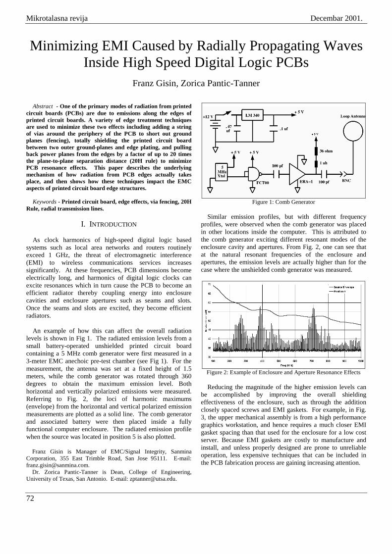
An example of how this can affect the overall radiation levels is shown in Fig 1. The radiated emission levels from a small battery-operated unshielded printed circuit board containing a 5 MHz comb generator were first measured in a 3-meter EMC anechoic pre-test chamber (see Fig 1). For the measurement, the antenna was set at a fixed height of 1.5 meters, while the comb generator was rotated through 360 degrees to obtain the maximum emission level. Both horizontal and vertically polarized emissions were measured. Referring to Fig. 2, the loci of harmonic maximums (envelope) from the horizontal and vertical polarized emission measurements are plotted as a solid line. The comb generator and associated battery were then placed inside a fully functional computer enclosure. The radiated emission profile when the source was located in position 5 is also plotted. Franz Gisin is Manager of EMC/Signal Integrity, Sanmina Corporation, 355 East Trimble Road, San Jose 95111. E-mail: [email protected]. Dr. Zorica Pantic-Tanner is Dean, College of Engineering, University of Texas, San Antonio. E-mail: [email protected].
Figure 1: Comb Generator
Similar emission profiles, but with different frequency
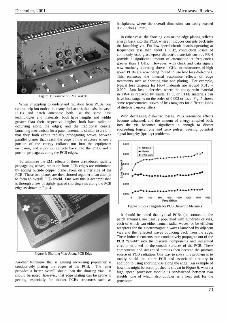
profiles, were observed when the comb generator was placed in other locations inside the computer. This is attributed to the comb generator exciting different resonant modes of the enclosure cavity and apertures. From Fig. 2, one can see that at the natural resonant frequencies of the enclosure and apertures, the emission levels are actually higher than for the case where the unshielded comb generator was measured.
Figure 2: Example of Enclosure and Aperture Resonance Effects
Reducing the magnitude of the higher emission levels can
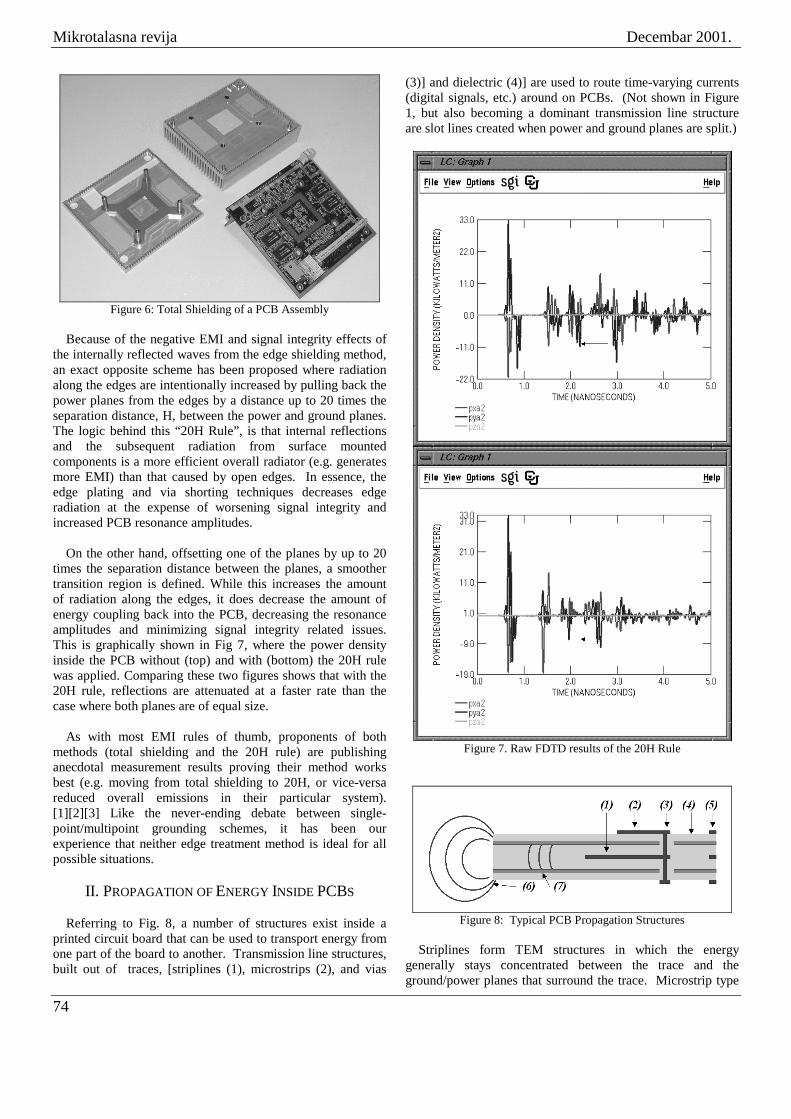
be accomplished by improving the overall shielding effectiveness of the enclosure, such as through the addition closely spaced screws and EMI gaskets. For example, in Fig. 3, the upper mechanical assembly is from a high performance graphics workstation, and hence requires a much closer EMI gasket spacing than that used for the enclosure for a low cost server. Because EMI gaskets are costly to manufacture and install, and unless properly designed are prone to unreliable operation, less expensive techniques that can be included in the PCB fabrication process are gaining increasing attention.
December, 2001 Microwave Review
73
Figure 3: Example of EMI Gaskets
When attempting to understand radiation from PCBs, one
cannot help but notice the many similarities that exist between PCBs and patch antennas: both use the same base technologies and materials; both have lengths and widths greater than their respective heights; both have radiation occurring along the edges; and the traditional coaxial launching mechanism for a patch antenna is similar to a via in that they both excite radially propagating waves between parallel planes that reach the edge of the structure where a portion of the energy radiates out into the equipment enclosure, and a portion reflects back into the PCB, and a portion propagates along the PCB edges.
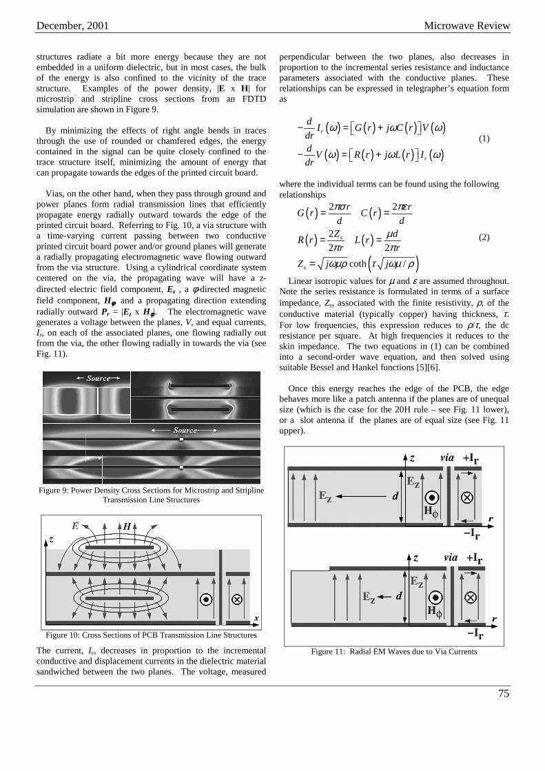
To minimize the EMI effects of these via-induced radially propagating waves, radiation from PCB edges are minimized by adding outside copper plane layers on either side of the PCB. These two planes are then shorted together in an attempt to form an overall PCB shield. One way this is accomplished is through a row of tightly spaced shorting vias along the PCB edge as shown in Fig. 4.
Figure 4: Shorting Vias Along PCB Edge
Another technique that is gaining increasing popularity is conductively plating the edges of the PCB. The latter provides a better overall shield than the shorting vias. It should be noted, however, that edge plating can be prone to peeling, especially for thicker PCBs structures such as
backplanes, where the overall dimension can easily exceed 0.25 inches (6 mm).
In either case, the shorting vias or the edge plating reflects energy back into the PCB, where it induces currents back into the launching via. For low speed circuit boards operating at frequencies less than about 1 GHz, conduction losses of commonly used glass-epoxy dielectric materials such as FR-4 provide a significant amount of attenuation at frequencies greater than 1 GHz. However, with clock and data signals now routinely operating above 1 GHz, manufacturers of high speed PCBs are now being forced to use low loss dielectrics. This enhances the internal resonance effects of edge treatments such as shorting vias and plating. For example, typical loss tangents for FR-4 materials are around 0.015 – 0.020. Low loss dielectrics, where the epoxy resin material in FR-4 is replaced by Imide, PPE, or PTFE materials can have loss tangents on the order of 0.003 or less. Fig. 5 shows some representative curves of loss tangents for different kinds of dielectric epoxy fillers.
With decreasing dielectric losses, PCB resonance effects become enhanced, and the amount of energy coupled back into the via becomes significant e enough to distort succeeding logical one and zero pulses, causing potential signal integrity (quality) problems.
Figure 5: Loss Tangents for PCB Dielectric Materials
It should be noted that typical PCBs (in contrast to the
patch antenna), are usually populated with hundreds of vias, each of which can either launch radial waves, or be efficient receptors for the electromagnetic waves launched by adjacent vias and the reflected waves bouncing back from the edge. These induced currents then conductively propagate out of the PCB “shield” into the discrete components and integrated circuits mounted on the outside surfaces of the PCB. These components and integrated circuits then become the primary source of PCB radiation. One way to solve this problem is to totally shield the entire PCB and associated circuitry in addition to using shorting vias along the edge. An example of how this might be accomplished is shown in Figure 6, where a high speed processor module is sandwiched between two shields, one of which also doubles as a heat sink for the processor.
Mikrotalasna revija Decembar 2001.
74
Figure 6: Total Shielding of a PCB Assembly
Because of the negative EMI and signal integrity effects of
the internally reflected waves from the edge shielding method, an exact opposite scheme has been proposed where radiation along the edges are intentionally increased by pulling back the power planes from the edges by a distance up to 20 times the separation distance, H, between the power and ground planes. The logic behind this “20H Rule”, is that internal reflections and the subsequent radiation from surface mounted components is a more efficient overall radiator (e.g. generates more EMI) than that caused by open edges. In essence, the edge plating and via shorting techniques decreases edge radiation at the expense of worsening signal integrity and increased PCB resonance amplitudes.
On the other hand, offsetting one of the planes by up to 20 times the separation distance between the planes, a smoother transition region is defined. While this increases the amount of radiation along the edges, it does decrease the amount of energy coupling back into the PCB, decreasing the resonance amplitudes and minimizing signal integrity related issues. This is graphically shown in Fig 7, where the power density inside the PCB without (top) and with (bottom) the 20H rule was applied. Comparing these two figures shows that with the 20H rule, reflections are attenuated at a faster rate than the case where both planes are of equal size.
As with most EMI rules of thumb, proponents of both methods (total shielding and the 20H rule) are publishing anecdotal measurement results proving their method works best (e.g. moving from total shielding to 20H, or vice-versa reduced overall emissions in their particular system). [1][2][3] Like the never-ending debate between single-point/multipoint grounding schemes, it has been our experience that neither edge treatment method is ideal for all possible situations.
II. PROPAGATION OF ENERGY INSIDE PCBS
Referring to Fig. 8, a number of structures exist inside a printed circuit board that can be used to transport energy from one part of the board to another. Transmission line structures, built out of traces, [striplines (1), microstrips (2), and vias
(3)] and dielectric (4)] are used to route time-varying currents (digital signals, etc.) around on PCBs. (Not shown in Figure 1, but also becoming a dominant transmission line structure are slot lines created when power and ground planes are split.)
Figure 7. Raw FDTD results of the 20H Rule
Figure 8: Typical PCB Propagation Structures
Striplines form TEM structures in which the energy
generally stays concentrated between the trace and the ground/power planes that surround the trace. Microstrip type
December, 2001 Microwave Review
75
structures radiate a bit more energy because they are not embedded in a uniform dielectric, but in most cases, the bulk of the energy is also confined to the vicinity of the trace structure. Examples of the power density, |E x H| for microstrip and stripline cross sections from an FDTD simulation are shown in Figure 9.
By minimizing the effects of right angle bends in traces through the use of rounded or chamfered edges, the energy contained in the signal can be quite closely confined to the trace structure itself, minimizing the amount of energy that can propagate towards the edges of the printed circuit board.
Vias, on the other hand, when they pass through ground and power planes form radial transmission lines that efficiently propagate energy radially outward towards the edge of the printed circuit board. Referring to Fig. 10, a via structure with a time-varying current passing between two conductive printed circuit board power and/or ground planes will generate a radially propagating electromagnetic wave flowing outward from the via structure. Using a cylindrical coordinate system centered on the via, the propagating wave will have a z-directed electric field component, Ez , a φ-directed magnetic field component, Hφφφφ, and a propagating direction extending radially outward Pr = |Ez x Hφφφφ|. The electromagnetic wave generates a voltage between the planes, V, and equal currents, Ir, on each of the associated planes, one flowing radially out from the via, the other flowing radially in towards the via (see Fig. 11).
Figure 9: Power Density Cross Sections for Microstrip and Stripline
Transmission Line Structures
Figure 10: Cross Sections of PCB Transmission Line Structures
The current, Ir, decreases in proportion to the incremental conductive and displacement currents in the dielectric material sandwiched between the two planes. The voltage, measured
perpendicular between the two planes, also decreases in proportion to the incremental series resistance and inductance parameters associated with the conductive planes. These relationships can be expressed in telegrapher’s equation form as
( ) ( ) ( ) ( )
( ) ( ) ( ) ( )
r
r
d I G r j C r Vdrd V R r j L r Idr
ω ω ω
ω ω ω
− = +
− = +
(1)
where the individual terms can be found using the following relationships
( ) ( )
( ) ( )
( )
2 2
22 2
coth /
s
s
r rG r C rd d
Z dR r L rr r
Z j j
πσ πε
µπ π
ωµρ τ ωµ ρ
= =
= =
=
(2)
Linear isotropic values for µ and ε are assumed throughout. Note the series resistance is formulated in terms of a surface impedance, Zs, associated with the finite resistivity, ρ, of the conductive material (typically copper) having thickness, τ. For low frequencies, this expression reduces to ρ/τ, the dc resistance per square. At high frequencies it reduces to the skin impedance. The two equations in (1) can be combined into a second-order wave equation, and then solved using suitable Bessel and Hankel functions [5][6].
Once this energy reaches the edge of the PCB, the edge behaves more like a patch antenna if the planes are of unequal size (which is the case for the 20H rule – see Fig. 11 lower), or a slot antenna if the planes are of equal size (see Fig. 11 upper).
Figure 11: Radial EM Waves due to Via Currents
Mikrotalasna revija Decembar 2001.
76
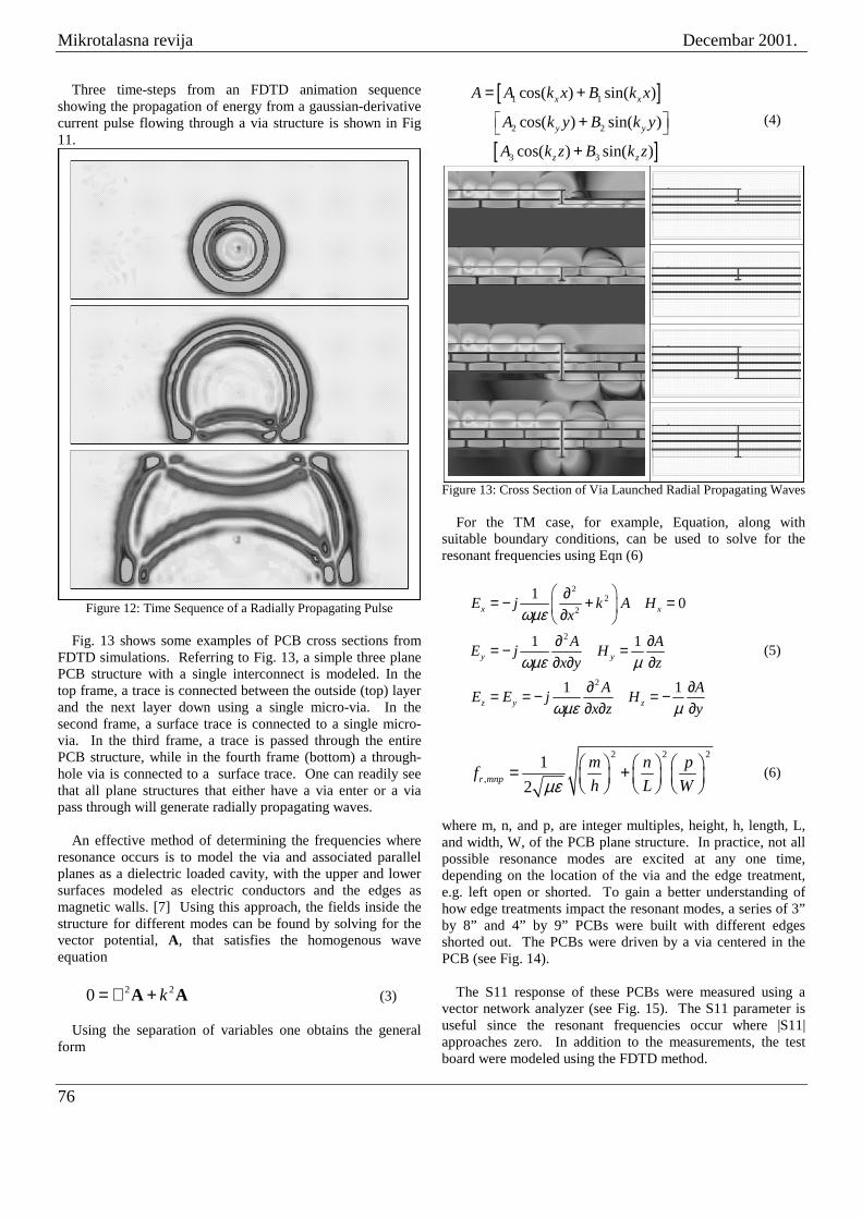
Three time-steps from an FDTD animation sequence showing the propagation of energy from a gaussian-derivative current pulse flowing through a via structure is shown in Fig 11.
Figure 12: Time Sequence of a Radially Propagating Pulse
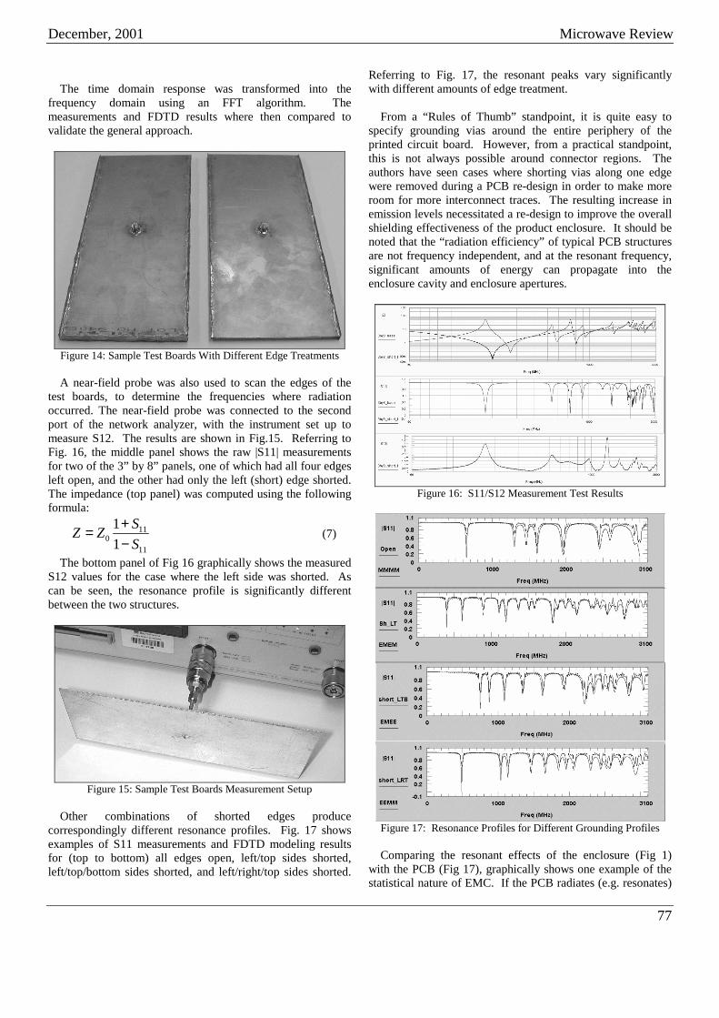
Fig. 13 shows some examples of PCB cross sections from
FDTD simulations. Referring to Fig. 13, a simple three plane PCB structure with a single interconnect is modeled. In the top frame, a trace is connected between the outside (top) layer and the next layer down using a single micro-via. In the second frame, a surface trace is connected to a single micro-via. In the third frame, a trace is passed through the entire PCB structure, while in the fourth frame (bottom) a through-hole via is connected to a surface trace. One can readily see that all plane structures that either have a via enter or a via pass through will generate radially propagating waves.
An effective method of determining the frequencies where resonance occurs is to model the via and associated parallel planes as a dielectric loaded cavity, with the upper and lower surfaces modeled as electric conductors and the edges as magnetic walls. [7] Using this approach, the fields inside the structure for different modes can be found by solving for the vector potential, A, that satisfies the homogenous wave equation 2 20 k= ∇ +A A (3)
Using the separation of variables one obtains the general form
[ ]
[ ]
1 1
2 2
3 3
cos( ) sin( )
cos( ) sin( )
cos( ) sin( )
x x
y y
z z
A A k x B k x
A k y B k y
A k z B k z
= +
+
+
(4)
Figure 13: Cross Section of Via Launched Radial Propagating Waves
For the TM case, for example, Equation, along with suitable boundary conditions, can be used to solve for the resonant frequencies using Eqn (6)
22
2
2
2
1 0
1 1
1 1
x x
y y
z y z
E j k A Hx
A AE j Hx y z
A AE E j Hx z y
ωµε
ωµε µ
ωµε µ
∂= − + = ∂
∂ ∂= − =∂ ∂ ∂
∂ ∂= = − = −∂ ∂ ∂
(5)
2 2 2
,1
2r mnpm n pfh L Wµε
= +
(6)
where m, n, and p, are integer multiples, height, h, length, L, and width, W, of the PCB plane structure. In practice, not all possible resonance modes are excited at any one time, depending on the location of the via and the edge treatment, e.g. left open or shorted. To gain a better understanding of how edge treatments impact the resonant modes, a series of 3” by 8” and 4” by 9” PCBs were built with different edges shorted out. The PCBs were driven by a via centered in the PCB (see Fig. 14).
The S11 response of these PCBs were measured using a
vector network analyzer (see Fig. 15). The S11 parameter is useful since the resonant frequencies occur where |S11| approaches zero. In addition to the measurements, the test board were modeled using the FDTD method.
December, 2001 Microwave Review
77
The time domain response was transformed into the
frequency domain using an FFT algorithm. The measurements and FDTD results where then compared to validate the general approach.
Figure 14: Sample Test Boards With Different Edge Treatments
A near-field probe was also used to scan the edges of the
test boards, to determine the frequencies where radiation occurred. The near-field probe was connected to the second port of the network analyzer, with the instrument set up to measure S12. The results are shown in Fig.15. Referring to Fig. 16, the middle panel shows the raw |S11| measurements for two of the 3” by 8” panels, one of which had all four edges left open, and the other had only the left (short) edge shorted. The impedance (top panel) was computed using the following formula:
110
11
11
SZ ZS
+=−
(7)
The bottom panel of Fig 16 graphically shows the measured S12 values for the case where the left side was shorted. As can be seen, the resonance profile is significantly different between the two structures.
Figure 15: Sample Test Boards Measurement Setup
Other combinations of shorted edges produce
correspondingly different resonance profiles. Fig. 17 shows examples of S11 measurements and FDTD modeling results for (top to bottom) all edges open, left/top sides shorted, left/top/bottom sides shorted, and left/right/top sides shorted.
Referring to Fig. 17, the resonant peaks vary significantly with different amounts of edge treatment.
From a “Rules of Thumb” standpoint, it is quite easy to specify grounding vias around the entire periphery of the printed circuit board. However, from a practical standpoint, this is not always possible around connector regions. The authors have seen cases where shorting vias along one edge were removed during a PCB re-design in order to make more room for more interconnect traces. The resulting increase in emission levels necessitated a re-design to improve the overall shielding effectiveness of the product enclosure. It should be noted that the “radiation efficiency” of typical PCB structures are not frequency independent, and at the resonant frequency, significant amounts of energy can propagate into the enclosure cavity and enclosure apertures.
Figure 16: S11/S12 Measurement Test Results
Figure 17: Resonance Profiles for Different Grounding Profiles
Comparing the resonant effects of the enclosure (Fig 1)
with the PCB (Fig 17), graphically shows one example of the statistical nature of EMC. If the PCB radiates (e.g. resonates)
Mikrotalasna revija Decembar 2001.
78
at a frequency where the enclosure cavity and/or apertures do not resonate, then relatively little energy will ultimately radiate out of the enclosure. However, if multiple combinations of PCB, enclosure cavity, and aperture resonances occur at the same frequency, then a significant amount of energy can radiate. The EMC community is littered with anecdotal test and measurement results where moving an interface card from one location to another within the same enclosure can produce widely varying radiated emission levels because different resonant modes (that were not excited before) get excited depending on where the interface card is positioned within the cavity.
In actual PCBs the dielectric material surrounding the ground and power planes usually extend beyond the edge of the planes. Most printed circuit boards also have more than one set of ground/power planes. This produces more complex edge structures (as compared to a simple patch antenna) that not only include direct radiation, but coupling around the planes from one layer into another. The edge also forms a transmission line along which energy can circulate around the board, creating additional resonance modes. In these cases, the simplified models for a slotline radiator and patch antenna do not fully quantify the complexity of the edge structures.
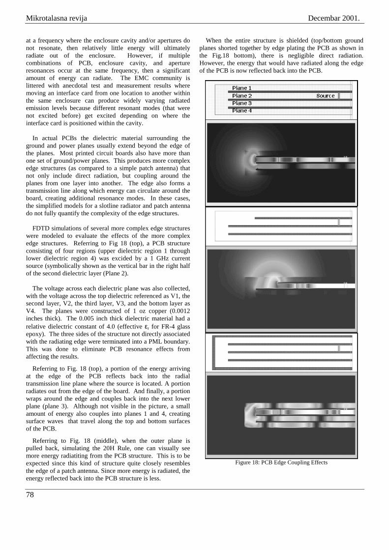
FDTD simulations of several more complex edge structures were modeled to evaluate the effects of the more complex edge structures. Referring to Fig 18 (top), a PCB structure consisting of four regions (upper dielectric region 1 through lower dielectric region 4) was excided by a 1 GHz current source (symbolically shown as the vertical bar in the right half of the second dielectric layer (Plane 2).
The voltage across each dielectric plane was also collected, with the voltage across the top dielectric referenced as V1, the second layer, V2, the third layer, V3, and the bottom layer as V4. The planes were constructed of 1 oz copper (0.0012 inches thick). The 0.005 inch thick dielectric material had a relative dielectric constant of 4.0 (effective εr for FR-4 glass epoxy). The three sides of the structure not directly associated with the radiating edge were terminated into a PML boundary. This was done to eliminate PCB resonance effects from affecting the results.
Referring to Fig. 18 (top), a portion of the energy arriving at the edge of the PCB reflects back into the radial transmission line plane where the source is located. A portion radiates out from the edge of the board. And finally, a portion wraps around the edge and couples back into the next lower plane (plane 3). Although not visible in the picture, a small amount of energy also couples into planes 1 and 4, creating surface waves that travel along the top and bottom surfaces of the PCB.
Referring to Fig. 18 (middle), when the outer plane is pulled back, simulating the 20H Rule, one can visually see more energy radiatiting from the PCB structure. This is to be expected since this kind of structure quite closely resembles the edge of a patch antenna. Since more energy is radiated, the energy reflected back into the PCB structure is less.
When the entire structure is shielded (top/bottom ground planes shorted together by edge plating the PCB as shown in the Fig.18 bottom), there is negligible direct radiation. However, the energy that would have radiated along the edge of the PCB is now reflected back into the PCB.
Figure 18: PCB Edge Coupling Effects

December, 2001 Microwave Review
79
A relative measure of coupling from one layer to another can be described by the voltage developed across the respective dielectric materials. Table 1 lists the voltage maximums across each dielectric surface as computed from the FDTD simulation. The voltage was measured half way between the source and the edge of the structure. Referring to Table 1, column 2, one can see the voltage in reference plane 2, is highest with the flat edge structure (Fig 18 top), indicating a high standing wave pattern due to the relatively large amounts of energy reflected back from the edge. One can also see relatively little energy coupled around the edge of the structure into the adjacent planes above and below the launch plane, as reflected in relatively low voltage drops across their respective dielectrics.
TABLE 1
VOLTAGES ACROSS PCB PLANE STRUCTURES
Voltage/Plane
Flat Edge
Pulled Back Edge
Total Shielding
1 0.009 0.024 0.216 2 1.452 0.895 1.336 3 0.100 0.026 0.223 4 0.006 0.005 0.258
When the upper plane is pulled back, the voltage in the upper dielectric increases significantly (0.024/0.009), while the voltages in the other planes decrease. And finally, with total shielding, the voltages in plane 2 again increases to approximately the value obtained for the flat edge simulation. The voltages for the other layers also increase significantly.
III. CONCLUSIONS
One of the primary printed circuit board mechanisms that produce radiated from PCB edges are via currents that excite radially propagating electromagnetic waves between power and/or ground plane structures. When these waves reach the edge of the printed circuit boards, a portion of the energy radiates into space (usually the cavity of the electronic enclosure housing the PCBs), and a portion is reflected back into the PCB, where it induces currents into the same vias that were the original source of the initial radially propagating wave. These induced currents then conductively flow into the components mounted on the surface of the PCB, producing secondary radiation. The waves inside the PCB excite resonant modes whose frequencies are dependent on the
length and with of the PCB, as well as the type of edge treatment used to reduce radiation. The most common technique of reducing edge radiation is fencing, where a series of shorting vias are used to connect top/bottom ground planes into a Faraday shield. This increases internal reflections. An alternate approach is to pull back one of the ground/power planes to form a smoother impedance transition region. While this increases edge emissions, it reduces PCB resonance effects. It is not clear whether this latter method consistently produces an overall reduction in emission levels.
ACKNOWLEDGEMENTS
The authors would like to thank Bill Panos for the
construction, FDTD modeling, and measurements associated with the sample test boards used in this paper.
REFERENCES
[1] Ye Xiaoning, Hockanson, David M., Li, Min, Cui, Wei, Radu,
Sergiu, Drewniak, James L., “The EMI Benefits of Ground Plane Stitching in Multi-Layer Power Bus Stacks”, 2000 IEEE EMC International Symposium, Washington D.C.
[2] Hirayr M. Kudyan, “Role of Interactions Between Hardware
Units and Card-Cage Structural Members in the Coupling of On-Board EM1 Fields to Currents on the Outer Surfaces of the Card-Cage Structure”, 2000 IEEE EMC International Symposium, Washington D.C.
[3] Gisin, Franz, Pantic-Tanner, Z., “Radiation From Printed
Circuit Board Edge Structures”, 2001 IEEE EMC International Symposium, Montreal, Canada.
[4] Robert G. Kaires, “Radiated Emissions from Printed Circuit
Board Traces Including the Effect of Vias, as a Function of Source, Termination and Board Characteristics”, 1988 IEEE EMC International Symposium.
[5] Ramo, Whinnery, and Van Duzer “Fields and Waves in
Communication Electronics”, 1965, John Wiley & Sons. [6] Parker, James C., “Via Coupling Within Parallel Rectangular
Planes”, IEEE Transactions on Electromagnetic Compatibility, Vol 39, No 1, February 1997.
[7] Balanis, Constantine, Antenna Theory, Analysis and Design,
Second Edition, 1997, John Wiley and Sons, pp.736-752.