miniaturized printed wire antenna for wireless communications
TRANSCRIPT

358 IEEE ANTENNAS AND WIRELESS PROPAGATION LETTERS, VOL. 4, 2005
Miniaturized Printed Wire Antennafor Wireless Communications
H. Y. David Yang, Fellow, IEEE
Abstract—Miniaturized printed-circuit-board wire antennas areinvestigated for wireless local access network (WLAN) and Blue-tooth applications. The proposed wire antenna in F shape couldhave a much smaller area than an inverted F antenna with sim-ilar bandwidth. It is found an F antenna can usually be inductivelytuned but the bandwidth decreases if the size is reduced from aquarter wave length. The bandwidth as a function of the antennavertical and parallel arm lengths is characterized with numericalsimulations. The antenna with an area of about 14 mm by 6 mm for2.4 GHz industrial, scientific, and medical (ISM) band, similar tothe size of a chip, is designed and tested with a bandwidth of about200 MHz. The antenna range and blind spot are also discussed.
Index Terms—Printed circuits, radiation, wire antennas, wire-less communication.
I. INTRODUCTION
RECENTLY, there is a worldwide demand for the develop-ment of wireless communication systems for local access
networks (WLAN) including Bluetooth, IEEE 802.11a, and802.11b. This demand has stirred significant renewed interestin antenna designs at the industrial, scientific, and medical(ISM) band. Many novel antenna structures for single, dual,or multiple bands have been proposed [1], [2]. Commercialproducts including Murata chip antennas (by Murata Co.),blue-chip antennas (by Centurion Co.), etc. are readily available.However, in a cost-effective personal communication system,the front-end antenna should be integrated on the circuit boardwith a minimum area and with more than 100 MHz bandwidthat 2.4 GHz ISM band. Printed circuit antennas are desirable fortheir low cost, low profile, and conformality [3]. A commondrawback is the narrow bandwidth, when a conductor backingis presented. Parasitic elements may be used to provide multipleresonances to enhance the bandwidth. Recently, inverted printedF antennas were proposed that provide a much wider bandwidthand smaller size [4] by removing the ground backing underneaththe wire antenna. An inverted F antenna [5], [6] is similar toa freestanding quarter-wave monopole above a ground plane,rather than the usual half-wave wire antennas. Much largerbandwidth is a result of a lower Q-factor as compared to theresonant microstrip elements. Inverted F antennas on a circuitboard provide a broadband miniaturized antenna solution. InWLAN or Bluetooth applications where the complete com-munication system is in a single chip built on a small circuitboard, it usually allows very small area for an antenna. There isa demand that the antenna area be less than 10 mm by 10 mm on
Manuscript received April 25, 2005; revised July 19, 2005.The author is with the Department of Electrical and Computer Engi-
neering, University of Illinois at Chicago, Chicago, IL 60607 USA (e-mail:[email protected]).
Digital Object Identifier 10.1109/LAWP.2005.857033
Fig. 1. Top view of a printed inverted F and a straight F antenna on a printedcircuit board (dash line shows the backing conductor cut).
a FR-4 substrate (dielectric constant 4.2). This presents a designand impedance matching problem. The inductive and capacitivearms of a printed inverted F antenna add up as the total antennalength that is usually much larger than what is desired. The in-ductive arm limits the flexibility in miniaturization. In this letter,a straight F antenna is investigated for further size reduction.The arm lengths of the F-shape wire antenna are optimized forbandwidth. The design and test results show that this antenna ismuch smaller than the usual inverted F antenna with sufficientbandwidth for the ISM band. Numerical results based on Ansofthigh frequency structure simulator (HFSS) characterize theantenna characteristics and provide a design guide line of thetradeoff between the antenna size and bandwidth.
II. PRINTED STRAIGHT F ANTENNA AND
ITS DESIGN CONSIDERATIONS
An example of a printed inverted F antenna is shown inFig. 1(a). A distinctive feature of this wire antenna is thatits antenna portion is in F shape and the opposite side of thesurface is without conductor backing. It can be viewed asa suspended inverted F antenna collapsing on the substratesurface. Without conductor on the back to form a resonator,it maintains the low-Q feature of a suspended antenna and isbroadband in nature. A 50 trace extends into antenna centralarm and it requires a conductor backing to form a microstriptransmission line. The conductor on the backside is also neces-sary as the ground for the chips and board circuits. A printedinverted F antenna is typically placed at the edge (corner) of acircuit board where only near the corner edge part of the metalground is removed. The right arm of the feed trace acts as acapacitor, while the left arm is used for inductive tuning. Thiswire antenna is similar to a wire travelling-wave antenna [5]and at the resonance the input resistor is close to 50 , the
1536-1225/$20.00 © 2005 IEEE

YANG: MINIATURIZED PRINTED WIRE ANTENNA FOR WIRELESS COMMUNICATIONS 359
Fig. 2. Impedance bandwidth versus the antenna length (the length ismeasured from the truncated ground plane to the open trace). The centerfrequency is at 2.4 GHz.
characteristic impedance of the feed trace. The capacitive armlength is designed as a quarter-wave monopole.
For WLAN and Bluetooth personal communication systemsapplications, the dimensions of overall communication systemsare fairly small, while the required bandwidth is 80 MHz (2.4 to2.48 GHz). The board space left for an antenna is usually verylimited. In this letter, we discuss a straight printed F antenna tofurther reduce the antenna dimension. The top view of a printedstraight F is shown in Fig. 1(b). For an inverted F antenna, ca-pacitive and inductive arms are on either side of the feed lineresulting in a longer lateral antenna dimension. For a straight F,the inductive tuning arm is placed inside the L-shape capacitivearm. The inductive arm is printed right above the ground planeedge as a board circuit element. The wire antenna is bent in anF shape such that the antenna could be placed effectively on thecorner of a circuit board. An interesting design problem is to de-termine the smallest antenna area to satisfy minimum bandwidthrequirement. The bandwidth as a function of the antenna length(the wire extension beyond the ground plane edge) for a straightwire antenna is investigated using Ansoft HFSS. The numericalresults are shown in Fig. 2 for a 30 mil FR-4 substrate and a 50
transmission line tuned at 2.4 GHz. It is seen that maximumbandwidth (800 MHz or 33%) occurs when the antenna lengthis about a quarter wavelength long. The increase or decrease ofthe antenna length reduces the bandwidth. The input impedanceof the monopole antenna shown in Fig. 2, excludingthe tuning inductor is given as
(1)
When the RC time constant is sufficiently large as is usually thecase when the monopole is close to a quarter of a wavelength(quarter-wave transformerfromanopen), theadmittance[inverseof (1)] is approximated as
(2)
It is seen from (2) that the antenna admittance is frequency insen-sitive (imaginary part is very small). This observation explainsthe broadband nature of the antenna. For wireless applications atISM bands, the required bandwidth is only about 3% (80 MHz at
Fig. 3. Impedance bandwidth versus the antenna vertical length H1 (totallength is fixed). The center frequency is at 2.4 GHz.
Fig. 4. Printed straight F antenna on a FR-4 substrate with the detail antennadimensions. Microstrip line width is 0.24 mm and substrate thickness is 5 mil.
2.4 GHz) and the design should be at least 5% to accommodatethe environmental factors, suggesting that the antenna length canbe much smaller than a quarter of a wavelength as seen in Fig. 2.
There are further design considerations when the wire antennais bent in an F shape at the board corner. In general, the electricallength is shorterwhen theantenna ismovedtoward theboardedgefrom the middle, a result of the less effective dielectric constant.This implies that for the same bandwidth, the antenna is largerwhen it is placed at the corner. In addition, the area without theground backing is strictly for antenna purpose and should be assmall as possible. The part of a PCMCIA card extended out of alaptop computer is an example. It is desirable to have most of theantenna tracesbent towardand in parallel to theground.However,theparallelarmcreatesanoppositeimagecurrentandformsahighQ resonator with the ground. As a result, the longer the parallelarm (smaller antenna area with the same total antenna length), thesmaller thebandwidthwillbe.AnexampleoftheHFSSnumericalresults of bandwidth versus the bend length is shown in Fig. 3.It is observed that the bandwidth decrease significantly if thevertical arm H1 is small (or the parallel arm H2 is too close tothe ground) when the total antenna length is fixed. The results inFig. 3 provide a design guide line on how much bend one couldafford for a given desired bandwidth.
III. A DESIGN EXAMPLE
A design example of a meandered straight F antenna is shownin Fig. 4. The parallel arm is meandered to further reduce theantenna area. The overall antenna area is reduced down to below
360 IEEE ANTENNAS AND WIRELESS PROPAGATION LETTERS, VOL. 4, 2005
Fig. 5. Measured and simulated return loss versus frequency for the straight Fantenna.
14 mm by 6 mm for a 4-layer stack-up FR-4 substrate of 18 miloverall thickness for a 2.4 GHz band operation. The substratehas a truncated ground plane on the second and the bottomlayers indicated in the dark area in Fig. 4. Antenna is built onthe upper-left corner of the board with 7 mm extension of boardbeyond the ground plane. The top sandwiched substrate is 5 milthickness so that 50 ohm line trace is about 10 mil wide. De-tailed drawing is also shown in Fig. 4. Return loss measure-ment is performed with a network analyzer through on-surfaceprobing. Both simulated and measurement results are shown inFig. 5 with good agreement found. For 2.4 GHz band wirelesscommunications, the required bandwidth is about 80 MHz. Thedesigned antenna has bandwidth of about 200 MHz, sufficientfor the required applications. The F antenna can be miniatur-ized further by reducing the bandwidth. A 9 mm by 8 mm an-tenna with a bandwidth of 120 MHz was made for a Bluetoothdongle [7].
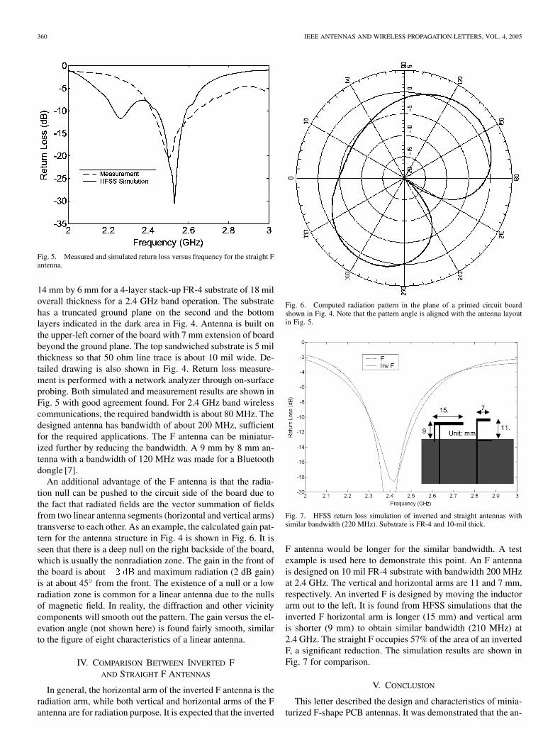
An additional advantage of the F antenna is that the radia-tion null can be pushed to the circuit side of the board due tothe fact that radiated fields are the vector summation of fieldsfrom two linear antenna segments (horizontal and vertical arms)transverse to each other. As an example, the calculated gain pat-tern for the antenna structure in Fig. 4 is shown in Fig. 6. It isseen that there is a deep null on the right backside of the board,which is usually the nonradiation zone. The gain in the front ofthe board is about and maximum radiation (2 dB gain)is at about 45 from the front. The existence of a null or a lowradiation zone is common for a linear antenna due to the nullsof magnetic field. In reality, the diffraction and other vicinitycomponents will smooth out the pattern. The gain versus the el-evation angle (not shown here) is found fairly smooth, similarto the figure of eight characteristics of a linear antenna.
IV. COMPARISON BETWEEN INVERTED FAND STRAIGHT F ANTENNAS
In general, the horizontal arm of the inverted F antenna is theradiation arm, while both vertical and horizontal arms of the Fantenna are for radiation purpose. It is expected that the inverted
Fig. 6. Computed radiation pattern in the plane of a printed circuit boardshown in Fig. 4. Note that the pattern angle is aligned with the antenna layoutin Fig. 5.
Fig. 7. HFSS return loss simulation of inverted and straight antennas withsimilar bandwidth (220 MHz). Substrate is FR-4 and 10-mil thick.
F antenna would be longer for the similar bandwidth. A testexample is used here to demonstrate this point. An F antennais designed on 10 mil FR-4 substrate with bandwidth 200 MHzat 2.4 GHz. The vertical and horizontal arms are 11 and 7 mm,respectively. An inverted F is designed by moving the inductorarm out to the left. It is found from HFSS simulations that theinverted F horizontal arm is longer (15 mm) and vertical armis shorter (9 mm) to obtain similar bandwidth (210 MHz) at2.4 GHz. The straight F occupies 57% of the area of an invertedF, a significant reduction. The simulation results are shown inFig. 7 for comparison.
V. CONCLUSION
This letter described the design and characteristics of minia-turized F-shape PCB antennas. It was demonstrated that the an-

YANG: MINIATURIZED PRINTED WIRE ANTENNA FOR WIRELESS COMMUNICATIONS 361
tenna area is much reduced as compared to an inverted F bymoving the inductive tuning arm into the ground-plane coveredarea. The main reason is that the both the vertical and horizontalarms are for radiation purpose. In contrast, in an inverted F, mostradiation is due to the horizontal arm. The F antenna is mostsuitable at the corner of a circuit board. The tradeoff betweenantenna size (vertical and parallel length) and bandwidth wasdiscussed. It was found that for miniaturized antenna designs,the parallel arm reduces and vertical arm enhances the band-width. A 2.4-GHz ISM band antenna was designed and tested.The designed F antenna has the performance of 200 MHz band-width with an area of 14 mm by 6 mm. The proposed antennastructure should find useful applications in WLAN or Bluetoothwhere the antenna length and width need to be flexible to fit intoa small area.
ACKNOWLEDGMENT
The author would like to thank N. C. Azenui for help withHFSS simulations.
REFERENCES
[1] M. Ali, “Analysis of integrated inverted-F antenna for Bluetooth applica-tions,” in Proc. 2000 IEEE Antennas and Propagation Society Conf. An-tennas and Propagation for Wireless Communications, Waltham, MA,pp. 21–24.
[2] R. Ramirez, H. Elsadek, L. Jofre, and D. Flaviis, “Reduced size singleand dual band linear polarized microstrip antennas for mobile commu-nications,” in Proc. 2001 IEEE Antennas and Propagation Society Int.Symp., vol. 4, Boston, MA, pp. 450–453.
[3] J. R. James, P. S. Hall, and C. Wood, Microstrip Antennas. Stevenage,U.K.: Peregrinus, 1981.
[4] C. Soras, M. karaboikis, G. Tsachtsiris, and V. Makios, “Analysis anddesign of an inverted-F antenna printed on a PCMCIA card for the 2.4GHz ISM band,” IEEE Antennas Propag. Mag., vol. 44, no. 1, pp. 37–44,Feb. 2002.
[5] K. Hirasawa and M. Haneishi, Eds., Analysis, Design, and Measurementof Small and Low-Profile Antennas. Norwood, MA: Artech House,1992.
[6] Z. D. Liu, P. S. Hall, and D. Wake, “Dual-frequency planar inverted-Fantenna,” IEEE Trans. Antennas Propag., vol. 45, no. 10, pp. 1451–1457,Oct. 1997.
[7] H. Y. Yang, “Wireless Division,” Broadcom Co., San Jose, CA, InternalTech. Rep., 2002.