miniature magnetic sensors
TRANSCRIPT

Miniature Magnetic Sensors
by
Saman Nazari Nejad
A thesis
presented to the University of Waterloo
in fulfillment of the
thesis requirement for the degree of
Doctor of Philosophy
in
Electrical and Computer Engineering
Waterloo, Ontario, Canada, 2015
©Saman Nazari Nejad 2015

ii
AUTHOR'S DECLARATION
I hereby declare that I am the sole author of this thesis. This is a true copy of the thesis, including any
required final revisions, as accepted by my examiners.
I understand that my thesis may be made electronically available to the public.

iii
Abstract
Magnetic sensors are widely used in nearly all engineering and industrial sectors, including high-
density magnetic recording, navigation, target detection, anti-theft systems, non-destructive testing,
magnetic labeling, space research, and bio-magnetic measurements in the human body. Miniature
magnetic sensors with high sensitivity are particularly advantageous in biomedical and specialized
industrial applications.
Amongst the various extant magnetic sensors, Micro-Electro-Mechanical System (MEMS) and Giant
Magneto impedance (GMI) sensors have the ability to sense low levels of magnetic field in the order
of 10 millitesla as well as the space to be further miniaturized. In this thesis, MEMS and GMI sensors
are studied in detail both theoretically and experimentally. Multiphysics analyses have been
developed to provide a path to further investigate these two types of sensors for various sensor
configurations. Several prototype units are successfully developed, fabricated and tested to verify the
validity of these models.
MEMS reed sensors consist of tri-layer beams of Au/Ni/Au. The actuation of these sensors is initiated
by the magnetic force to maintain the continuity of magnetic field streamlines. The Ni layer is
deployed as the main magnetic core, and the gold layers are used to enhance the contact quality of the
switches. In this work, a unique fabrication process is developed that significantly reduces the number
of masking and lithography steps. As well, a detailed finite element method is presented to study the
behavior of these sensors and to optimize the device performance. The FEM study considers various
magnetic environments, providing a performance map for the sensors. Having a performance map is
essential for a system’s operation and for tracking its operational behavior. The study also considers
the effects of various device formations and packaging for these types of sensors. The generated
magnetic force is observed to be much higher than the required mechanical force for device actuation.
The GMI sensors exhibit many advantages over their conventional counterparts. In particular, thermal
stability and high sensitivity make GMI sensors attractive candidates for a wide range of applications.
The GMI sensors are based on concepts different from those for conventional giant magneto
resistance (GMR) sensors. GMI sensors have been under active research only in the past decade. In
this thesis, thin film multilayer GMI sensors are realized using microfabrication technology. The
fabricated sensors are tri-layers of Co73Si12B15 /Au./ Co73Si12B15 The thin film GMI sensors are
studied in detail using FEM simulation, and several sensors are developed, fabricated and tested to
work in the millitesla range. A post-processing step is proposed to optimize the performance of GMI

iv
sensors and to enhance their magnetic sensitivity. The post-processing characterization shows that
annealing the devices with a specific annealing cycle has the optimal effect of enhancing the magnetic
characteristics of CoSiB. The sensors are treated with this post-processing recipe, demonstrating a
considerable increase in their magneto impedance (MI) ratio. The research has made a contribution to
establishing the engineering foundation toward the development of low-cost miniature GMI magnetic
sensors for low field intensity applications.

v
Acknowledgements
I wish to express my sincere appreciation and gratefulness to my advisor Professor Raafat R.
Mansour for his knowledge, insight, valuable guidance, and continuous encouragement throughout
this research. He is always there when I need help. His advices always helped me not just in my thesis
but in all aspects of my life. Indeed, my gratitude to him cannot be expressed in a few words and it is
my honor to be his student.
I am grateful to Professor Edmond Cretu from University of British Columbia who served as the
external examiner of this thesis and provided constructive feedback. I am also grateful to the
members of my PhD examination committee, Professor Eihab Abdel-Rahman, Professor John Yeow,
Professor Simarjeet Saini,and Professor Siva Sivoththaman for their time and effort to improve the
quality of this thesis.
I am thankful to all members of the Centre for Integrated RF Engineering (CIRFE) research group not
only for their invaluable technical assistance but also for creating a warm, friendly, and welcoming
environment. In particular, Dr. Arash Akhavan Fomani has significantly contributed to the outcome
of this research through many stimulating discussions.
I am indebted to many wonderful friends who have supported me even in the cold rainy days of my
PhD studies. They have been always there to lend me a helping hand and made my time at Waterloo
an enjoyable experience full of unforgettable memories. I would also like to recognize my colleagues
Dr. Siamak Fouladi, Dr. Sara Sharifian Attar, Dr. Neil Sarak, Dr. Scott Chen, Dr. Hassan Mahboubi,
Mostafa Azizi, Oliver Wong, Ahmed Abdel Aziz, Bill Joley and Maziar Moradi.
I would also like to thank my officemate Grigory Chugunov, who made our office enjoyable for long
stays. Without him, the PhD days would not be fun at all. I also need to thank my friend Dr. Soheil
Kolouri, without him my life would have been all dark and boring.
Extended thanks go to my Mom and Dad for their support and patience during my education life.
They taught me how to start with A,B,C and finish with a Ph.D dissertation. I will never forget their
endless support and kindness and I cannot be thankful enough for their sacrifices. I am thankful to my
caring brother and sister, Soheil and Sara, they always ignite hope in me whenever I feel hopeless.
Last but not the least, a world of thanks goes to my friend and colleague, my love and my wife,
Narges Fallahi, who stood behind me throughout this journey. I am really grateful to her
collaboration, enthusiasm and support. Without her hopeful vision on the down days of my research
and encouragements on the up days, this work would be far from completion.

vi
Dedication
To my beautiful wife, Narges Fallahi
To my Mom and Dad, Farahnaz Aghili and Rahman Nazari Nejad

vii
Table of Contents
AUTHOR'S DECLARATION ............................................................................................................... ii
Abstract ................................................................................................................................................. iii
Acknowledgements ................................................................................................................................ v
Dedication ............................................................................................................................................. vi
Table of Contents ................................................................................................................................. vii
List of Figures ....................................................................................................................................... ix
List of Tables ........................................................................................................................................ xv
Chapter 1 Introduction ............................................................................................................................ 1
1.1 Motivation .............................................................................................................................. 3
1.2 Objectives ............................................................................................................................... 4
1.3 Thesis Outline ......................................................................................................................... 5
2 Chapter Two Literature Survey ..................................................................................................... 6
2.1 Conventional Magnetic Sensors ............................................................................................. 6
2.1.1 Induction Sensors ........................................................................................................... 6
2.1.2 Fluxgate Sensors ............................................................................................................. 7
2.1.3 Magnetoresistors ............................................................................................................. 9
2.1.4 Hall Effect Sensors ....................................................................................................... 10
2.1.5 SQUID Sensors ............................................................................................................ 12
2.1.6 Magnetodiode and Mangetotransistor Sensors ............................................................. 13
2.1.7 MEMS-Based Magnetic Sensors .................................................................................. 14
2.1.8 Giant Magneto-Impedance Sensors .............................................................................. 17
3 Chapter Three Multilayer MEMS Reed Sensors .......................................................................... 20
3.1 Introduction .......................................................................................................................... 20
3.1.1 Theory .......................................................................................................................... 21
3.2 Nickel-based Magnetic MEMS Reed Sensors ...................................................................... 23
3.2.1 Modeling and FEM Simulation .................................................................................... 23
3.2.2 Design and Mask-Making ............................................................................................ 33
3.2.3 Fabrication Process ....................................................................................................... 36
3.2.4 Experimental Setup and Measurements ....................................................................... 45
3.3 Tri-layer Magnetic MEMS Reed Sensors ............................................................................ 46
3.3.1 Modeling and FEM Simulation .................................................................................... 47

viii
3.3.2 Design Rules and Fabrication Process ......................................................................... 57
3.3.3 Test and Experiment .................................................................................................... 62
4 Chapter Four Giant Magneto-Impedance Thin film Magnetic Sensors ....................................... 64
4.1 Introduction .......................................................................................................................... 64
4.2 Theory .................................................................................................................................. 65
4.3 COMSOL FEM Simulation ................................................................................................. 72
4.3.1 Study the effect of thickness ........................................................................................ 79
4.4 Fabrication Process .............................................................................................................. 80
4.4.2 Test Setup and Measurement ....................................................................................... 84
5 Chapter Five Characterization of GMI material- CoSiB ............................................................. 99
5.1 Introduction .......................................................................................................................... 99
5.2 Fabrication and Post-Processing ........................................................................................ 100
5.3 Magnetic Characterizations................................................................................................ 101
5.3.1 Permeability Measurement ........................................................................................ 102
5.3.2 Hysteresis Loop and Magnetization ........................................................................... 104
5.3.3 Magnetization of CoSiB Layer in a layered structure ................................................ 106
5.4 Material Characterizations ................................................................................................. 107
5.4.1 Raman Spectroscopy .................................................................................................. 107
5.4.2 X-Ray Diffraction ...................................................................................................... 109
5.4.3 Energy Dispersive X-Ray Spectroscopy .................................................................... 111
5.5 Results and Discussion ...................................................................................................... 113
5.6 Experimental Tests on Tri-Layer Thin Film GMI Sensors ................................................ 114
6 Chapter Six Conclusions and Future Plans ................................................................................ 117
6.1 Future Works ..................................................................................................................... 118
Appendix A ........................................................................................................................................ 120
Theory and mathematical equations for MEMS REED Sensors ....................................................... 120
Appendix B ........................................................................................................................................ 130
Appendix C ........................................................................................................................................ 132
Detailed Microfabrication recipe used for MEMS Reed sensors ....................................................... 132
Bibliography ...................................................................................................................................... 137
ix
List of Figures
Figure 1-1 Comparison between magnetic sensors working range [1]. ................................................. 2
Figure 2-1 The basic fluxgate principle. The ferromagnetic core is excited by the ac current Iexc of
frequency f into the excitation winding. The core permeability μ(t) is therefore changing with 2f
frequency. If the measure dc field B0 is present, the associated core flux Φ(t) is also changing with 2f,
and voltage Vind is induced in the pickup (measuring) coil having N turns. ........................................ 7
Figure 2-2 Simplified fluxgate waveforms (a) in the zero field and (b) with measured field H0. ......... 8
Figure 2-3 Orientation of the magnetization of the ferromagnetic layers in a GMR spin valve for
different external fields H. (a) H = 0, the magnetization of the free ferromagnetic layer is
perpendicular to the magnetization of pinned ferromagnet, R = R(0). (b) Low resistant state, H
parallel to the magnetization of the pinned ferromagnet, R < R(0). (c) High resistant state, H directed
opposite to the magnetization of the pinned ferromagnet, R > R(0). (d) H large enough to unpin the
pinned ferromagnet, R < R(0). ............................................................................................................... 9
Figure 2-4 (a) Schematic of Hall Effect sensors and (b) examples of Hall Effect products. .............. 11
Figure 2-5 Schematic of SQUID sensor. .............................................................................................. 12
Figure 2-6 Schematic of a SQUID magnetometer. ............................................................................... 13
Figure 2-7 Picture showing the concept of the MEMS flux concentrator. Note that there is a space
between the substrate and the flux concentrators on the MEMS flaps [15]. ........................................ 15
Figure 2-8 (a) SEM microphotograph of a magnetic switch, (b) zoomed-in view of the contact part
[10]. ...................................................................................................................................................... 16
Figure 2-9 CMOS-MEMS magnetometer systems with integrated magnetic coil [41] ....................... 17
Figure 2-10 A Co-wire GMI sensor reported in [43] ........................................................................... 18
Figure 2-11 Schematic view of GMI element (a) top view (b) cross sectional view [38]. ................... 19
Figure 3-1 Schematic view of undeformed magnetic switch and a deformed one [8]. ........................ 22
Figure 3-2 Modeled magnetic MEMS switch in COMSOL 4.2 GUI................................................... 25
Figure 3-3 Meshing of modeled magnetic MEMS switch. .................................................................. 27
Figure 3-4 Shows the magnetic flux density in Tesla for case a). ........................................................ 28
Figure 3-5 Shows magnetic flux density contours for magnetic switches. .......................................... 29
Figure 3-6 Magnetic flux density streamlines between the beams for case a). .................................... 30
Figure 3-7 Whole magnetic model of the switches in the environment. .............................................. 30
Figure 3-8 Shows the magnetic flux density in Tesla for case b). ........................................................ 31
Figure 3-9 Magnetic flux density contours for case b). ........................................................................ 32

x
Figure 3-10 Magnetic flux density streamlines between the beams for case b). ................................. 32
Figure 3-11 Actuation of switch at 10 mT. .......................................................................................... 33
Figure 3-12 Final mask printed on glass. ............................................................................................. 36
Figure 3-13 The passivation dielectric layer above silicon substrate................................................... 37
Figure 3-14 Cr/Gold seed layer after patterning. ................................................................................. 37
Figure 3-15 Bottom electrode fabricated on top of the substrate. ........................................................ 37
Figure 3-16 Patterned anchor (the gold layer on top of PI is not shown to prevent misunderstanding).
............................................................................................................................................................. 38
Figure 3-17 Wafer after patterning anchor and dimples on PI. ............................................................ 38
Figure 3-18 Final structure before release. .......................................................................................... 39
Figure 3-19 Optical image of switch type 1 – simple cantilever. ........................................................ 39
Figure 3-20 Optical image of switch type 2 – minder hinge switches. ................................................ 40
Figure 3-21 Optical image of switch type 3 – narrow cantilever with wider tips. ............................... 40
Figure 3-22 Optical image of switch type 4 – two-array switches....................................................... 40
Figure 3-23 Optical image of switch type 4 – four-arrays switches. ................................................... 41
Figure 3-24 Optical image of tip of one cantilever showing the position of the upper beam with
respect to the lower one; dimples and release holes are shown here. .................................................. 41
Figure 3-25 Magnetic Reed SW- a) minder shape support SW – width 60um and length 380 um b)SW
– width 80um and length 400 um......................................................................................................... 42
Figure 3-26 An Array of 2 Magnetic Reed SW – width 60um and length 370 um. ............................ 43
Figure 3-27 An Array of 2 Magnetic Reed SW – width 60um and length 370 um (side view). ......... 44
Figure 3-28 Magnetic Reed SW type 2 – width 60um and length 270 um. ......................................... 44
Figure 3-29 Magnetic Reed SW with wide tip type 3 – width (w1: 20um, w2:60um) and length
500um. ................................................................................................................................................. 45
Figure 3-30 Photo of measurement setup and stage............................................................................. 46
Figure 3-31- The COMSOL geometry 2D sketch of MEMS read switches, for a a)tri-layer without
packaging, b) tri-layer with glass packaging and c) nickel tip gold beams with the packaging .......... 49
Figure 3-32 the 2D COMSOL simulation for a tri-layer MEMS without packaging, this graph
illustrates the vertical displacement of sensors beams in actuated condition (10 mT magnetic field).
As shown above, the upper beam is experiencing a 4 um downward displacement which is 4 times
greater than our 1 um designed gap. .................................................................................................... 50

xi
Figure 3-33 Surface plot of magnetic field on Tri-layer MEMS Reed switch with packaging, as shown
above, the sensing magnetic field for the actuation is 9-11 mT. .......................................................... 51
Figure 3-34 the surface plot of upper beam vertical displacement. ...................................................... 52
Figure 3-35 magnified projected out of place displacement of both beams. The blue color is
corresponded to upper beam with the downward movement whereas the red on is corresponded to the
upward movement of the bottom electrode .......................................................................................... 53
Figure 3-36 Simulation setup and 3D geometric design of MEMS read sensors. ................................ 54
Figure 3-37 Magnetic field distribution over sensor in an actuation step. ........................................... 55
Figure 3-38 Generated force eon the upper beam. In the positions with negative value the actuation
will happen. In this figure x axis represents x direction and the unit is micro meter. .......................... 56
Figure 3-39 Working map of the MEMS Reed sensors, a) when the poles of permanent magnet are in
line with longitude direction of the sensor and its moving in that direction, b) when the pole of
permanent magnet are perpendicular to the longitude direction of sensors and c) when the permanent
magnet is in line with the sensor but it’s moving out of the plane far from sensor. ............................. 57
Figure 3-40 Fabrication steps of trilayer MEMS Reed switches .......................................................... 58
Figure 3-41 Optical microscopic image of trilayer MEMS Reed sensors a) ........................................ 60
Figure 3-42 Optical microscopic image of trilayer MEMS Reed sensors b) ....................................... 61
Figure 3-43 Optical microscopic image of trilayer MEMS Reed sensors c) ........................................ 62
Figure 3-44 Summary of MEMS reed sensor actuation test................................................................. 63
Figure 4-1 Schematic drawing of multilayer MI element, a) cross sectional view b)top view [37]. ... 66
Figure 4-2 Plots of the MI ratio vs. reduced frequency 𝐯 = 𝛚𝛚𝛅 for a number of parameters 𝐝𝟏/𝐝 in
(a) and 𝛔𝟏/𝛔𝟐 in (b).Typical parameters used for calculation are:𝟒𝛑𝐌𝐬 = 𝟔𝟎𝟎𝟎 𝐆,𝐇𝐊 =
𝟗 𝐎𝐞, 𝛔𝟐 = 𝟒. 𝟓 × 𝟏𝟎𝟏𝟔 𝐬 − 𝟏 . To avoid the divergence of 𝛍𝐭 at 𝐇𝐞𝐱 = 𝐇𝐊𝐚𝐧𝐝 𝛚 = 𝟎 , a small
anisotropy deviation in 5° from y-axis is introduced, the spin relaxation constant is taken to be 0.2.
These magnetic parameters are used for all of the calculations [32]. ................................................... 69
Figure 4-3 The MI ratio as a function of 𝐇𝐞𝐱 for two frequencies v=0.04 and v=0.16, d=0.1um,
𝛔𝟐 = 𝟏. 𝟕 × 𝟏𝟎𝟏𝟕𝐬 − 𝟏and 𝛔𝟏𝛔𝟐 = 𝟏𝟐(related to NiFe/Cu/NiFe) [32]. ......................................... 70
Figure 4-4 Plots of the MI ratio vs. frequency with the film width as a parameter: d=0.5 um and
d_1=d_2. The calculation is related to CoFeSiB/Cu/CoFeSiB films [37]............................................ 71
Figure 4-5- The calculated dependence of μ’; the real part of effective permeability, on applied
external magnetostatic field Hext ........................................................................................................... 72
Figure 4-6 The calculated dependence of μ”; the imaginary part of effective permeability, on Hext ... 73

xii
Figure 4-7 Circumferential magnetic flux of the sensor at 1 MHz ...................................................... 74
Figure 4-8 Current density distribution along the cross section under the external field of 2400 A/m 75
Figure 4-9 Simulation results for impedance of the GMI sensor at 200 kHz ...................................... 76
Figure 4-10 Simulation results for impedance of the GMI sensor at 500 kHz .................................... 77
Figure 4-11 Simulation results for impedance of the GMI sensor at 1 MHz ....................................... 78
Figure 4-12 The impedance of sample for different ac frequencies under various external magnetic
fields. .................................................................................................................................................... 78
Figure 4-13 Left) impedance of R-50-30 GMI sensor with 2 um thickness at 1 MHz, Right)
impedance of R-50-30 GMI sensor with 1 um thickness at 1 MHz, .................................................... 79
Figure 4-14 Left) impedance of GMI sensor with 2 um thickness at 500 kHz, Right) impedance of
GMI sensor with 1 um thickness at 500 kHz, ...................................................................................... 79
Figure 4-15 Fabrication process sequence of GMI samples. ............................................................... 81
Figure 4-16 Undercut of CoSiB sample. .............................................................................................. 82
Figure 4-17 A view of one batch of fabricated sensors. Two categories of devices are shown in this
figure. ................................................................................................................................................... 83
Figure 4-18 Various types of minder shape GMI sensors. ................................................................... 83
Figure 4-19 DC probes and measuring the variation of impedance under magnetic field in GMI
samples. ................................................................................................................................................ 84
Figure 4-20 Schematic of measurement setup. .................................................................................... 85
Figure 4-21 The measurement setup. ................................................................................................... 85
Figure 4-22 Impedance magnitude and phase of Device R10-40-1. .................................................... 86
Figure 4-23 Impedance magnitude of Device R10-40-1 at1 and 10 MHz. .......................................... 87
Figure 4-24 Impedance magnitude of Device 50-30 at1 and 10 MHz. ................................................ 87
Figure 4-25 Schematic of magnetization process in magneto-thermal annealing step ........................ 89
Figure 4-26 Measured impedance of two different GMI devices with different dimensions. As
expected, the sensor demonstrates a substantial increase in impedance at higher excitation
frequencies. .......................................................................................................................................... 90
Figure 4-27 Wheatstone bridge and DUT in final sensor. ................................................................... 91
Figure 4-28 Impedance of GMI sample, R-50-30, measured in different magnetic fields in a
frequency sweep of 150 Hz to 10 MHz ............................................................................................... 92
Figure 4-29 Measured impedance for R-50-30 (this is the same sample as previous section) at
constant external magnetic fields over a frequency sweep .................................................................. 93

xiii
Figure 4-30 The measured impedance for GMI R-50-30 which suing both measurement methods. ... 94
Figure 4-31 A comparison of 3D simulation for GMI R-50-30 and the measured impedances captured
with Impedance analyzer (Blue) and Oscilloscope (Red) .................................................................... 95
Figure 4-32 Measured impedance for R-50-30 (this sample is post process at the optimal processing
condition) at constant external magnetic fields over a frequency sweep ............................................. 96
Figure 4-33 Impedance of R-50-30 sample annealed in optimized condition ...................................... 96
Figure 4-34 Comparison of experimental measurement and simulation results for frequency range of
1 MHz to 10 MHz. ............................................................................................................................... 97
Figure 4-35 Maximum GMI as a Function of frequncy ....................................................................... 98
Figure 5-1 The relative permeability of samples thermally treated for 3 h; (b) the same for samples
annealed for 4 h. ................................................................................................................................. 102
Figure 5-2 (a) The relative permeability of samples treated magneto-thermally for 3 h; (b) the same
for samples annealed for 4 h. .............................................................................................................. 102
Figure 5-3 (a) The hysteresis loop of samples thermally treated for 3 h; (b) the same samples annealed
for 4 h. The square marker shows the loop for the process with the highest permeability, and the
triangle marker is for the after fabrication (AF) sample. .................................................................... 105
Figure 5-4 (a) The hysteresis loop of samples magneto-thermally treated for 3 h; b) the same annealed
for 4 h. The square marker shows the loop for the process with the highest permeability, and the
triangle marker is for the after fabrication (AF) sample. .................................................................... 105
Figure 5-5 Schematic of annealing magnetization under a magneto-thermal post-process. It is shown
how the Weiss walls are breaking up and letting the domains be aligned to the external field. ........ 107
Figure 5-6 Raman spectroscopy for thermal post-processed samples. .............................................. 108
Figure 5-7 Raman spectroscopy for magneto-thermal post-processed samples. ................................ 108
Figure 5-8 XRD graphs of samples thermally treated for 3 and 4 h. .................................................. 110
Figure 5-9 XRD graph of samples magneto-thermally treated for 3 and 4 h. .................................... 110
Figure 5-10 EDX graph of a sample magneto-thermally treated for 3 h at 600 °C. It should be noted
the same graph is captured for all other samples. ............................................................................... 112
Figure 5-11 GMI thin film samples fabrication process flow a) sputtering and patterning of CoSiB b)
Deposition and patterning of Metal trace layer c) sputtering and patterning of CoSiB d) A 1-inch to 1-
inch die of glass wafer, containing the thin film GMI samples. ......................................................... 115
Figure 5-12 Measurement results of GMI R-50-30 in 500 kHz ac current. ...................................... 116
Figure 6-1 The three basic subdomains typically present at magnetic MEMS [8]............................. 121

xiv
Figure 6-2 Various configurations of a deformed body [8]. .............................................................. 124
Figure 0-1 Bottom electrode design rules. ......................................................................................... 130
Figure 0-2 Dektak of first layer (Ni) with 0.5KÅ tip, in the above fig , 6 units are covered which
results to 3 um .................................................................................................................................... 133

xv
List of Tables
Table 1-1 Category of Magnetic Sensor Applications [1] ...................................................................... 3
Table 3-1 Lithography mask layers ...................................................................................................... 35
Table 3-2 Layer Names, Thicknesses, and Mask Levels ..................................................................... 35
Table 4-1 Impedance Values for GMI R-50-30 at 500 kHz Measured with Agilent Impedance
Analyzer ............................................................................................................................................... 93
Table 4-2Measured Values for GMI R-50-30 in Oscilloscope Measurement of Impedance ............... 94
Table 5-1 High Peaks of The Relative Permeability for Different Post-Processing Conditions ........ 103
Table 5-2 X-Ray Diffractometer Parameters...................................................................................... 109
Table 5-3 EDX Captured Quantitative Results. The Main Elements are Highlighted ....................... 112


1
Chapter 1
Introduction
For decades, magnetic sensors have helped humans analyze and control thousands of applications.
Computers have nearly unlimited memory through the use of magnetic sensors in magnetic storage
disks and tape drives. Airplanes experience enhanced levels of safety because of the reliability of
noncontact switching employing magnetic sensing. Factories have improved productivity because of
the precise stability and low cost of magnetic sensors. There are many ways to sense magnetic fields,
most of which are based on the intimate connection between magnetic and electric phenomena. A
common priority of magnetic sensors in all applications is that magnetic sensors provide a stronger,
more reliable, and more maintenance-free technology compared to other sensor technologies [1-4].
A magnetic sensor is a system or device that can measure the magnitude of a magnetic field or each
of its vector components. Magnetic sensors can be classified into scalar magnetometers and vector
magnetometers according to whether they measure the magnitude or the vector components of the
magnetic field. The techniques usually encompass many aspects of physics and electronics.
Magnetic sensing techniques exploit a broad range of ideas and phenomena from the fields of
physics and material science. The common technologies used for magnetic field sensing include
induction coil sensors, fluxgate, optically pumped nuclear precession, superconducting quantum
interference device (SQUID), Hall Effect, giant magnetoresistance, magnetic tunnel junctions, giant
magnetoimpedance, magnetodiode and magnetotransistor, fiber optic and magneto-optic, and
microelectromechanical systems (MEMS)-based magnetic sensors. A list of the most commonly used
magnetic sensor technologies is given in Fig. 1.1, in which the sensitivities of these sensors are
indicated [1].

2
Magnetic Sensor Technology
Detectable Field (gauss)
10−10 10−6 10−2 102 106
1 Coil
Magnetometers
2 Fluxgate
3 Optically Pumped
4 Nuclear-Precession
5 SQUID
6 Hall Effect
7 Magnetoresistive
8 Magnetodiode
9 Magnetotransistor
10 Magneto Optical
11 Giant Magneto Impedance
12 MEMS Reed Switches
Figure 1-1 Comparison between magnetic sensors working range [1].
As can be seen, magnetic sensors have a broad range of applications (Table 1.1) [1]. For example,
ultra-sensitive magnetic sensors are able to detect tiny magnetic fields produced outside the brain by
neuronal currents, which can be used for diagnostic applications. High reliability non-contact
switching with magnetic sensors leads to enhanced safety standards in aircraft, and magnetic sensors
are also used in automobiles to detect positions in the engine crank shaft and wheel braking.
Computers have nearly unlimited memory through the application of magnetic sensors in magnetic
storage hard drives and tape drives.

3
Table 1-1 Category of Magnetic Sensor Applications [1]
1E-9T 1E-4T
Category 1 Category 2 Category 3
High Sensitivity Medium Sensitivity Low Sensitivity
Definition: Definition: Definition:
Measuring field gradients or differences due to induced (in Earth's field) or permanent dipole moments
Measuring perturbations in the magnitudes and/or direction of Earth's fields due to induced or permanent dipoles
Measuring fields stronger than Earth's magnetic field
Major Applications: Major Applications: Major Applications:
Brain function mapping Magnetic compass Noncontact switching magnetic anomaly detection Munitions fusing
Current measurement
Mineral prospecting Magnetic memory readout
Most Common Sensor: Most Common Sensor: Most Common Sensor:
SQUID Coil magnetometer Coil magnetometer Optically pumped Flux-gate Hall-Effect Sensor
Magnetoresistive Magnetoresistive
1.1 Motivation
In light of magnetic sensors’ nearly limitless applications, a magnetic sensor with a working range
in millitesla would be in high demand. This magnetic field range has applications in various
industries, such as biomedical devices, communication systems, and automobile and airplane
industries [1], [21], [27]. Indeed, the high demand for this range has been the driving motivation for
this thesis, the intent of which is to generate new magnetic sensors and applications in the millitesla
range. As shown in Figure 1-1 and discussed in Chapter 2, MEMS technology magnetic sensors and
GMI (giant-magneto impedance) magnetic sensors are able to perform well and accurately in this
range.
MEMS technology magnetic sensors normally use a mechanical moveable part to sense the
magnetic field, while the GMI type show a change in their impedance based on their materials and are

4
fabricated using thin film technology. In this study, both MEMS and GMI sensors are designed,
fabricated, and tested.
1.2 Objectives
The major objectives of this Ph.D. thesis work are:
The development of miniature MEMS reed magnetic sensors.
There is a limited number of publications about MEMS reed magnetic sensing. Moreover, those
MEMS reed magnetic sensors have a minimum length of 1000 microns and their beams have a
relatively large width of hundreds of microns. Based on the simulation results generated, their
sensitivity can increase by changing the beams’ thicknesses. Hence, the size of the devices was
reduced by an order of 5 to 10, and the devices were fabricated as small as 20 to 80 um in width and
100 to 400 um in length. This reduction in size will ultimately help us offer an array of magnetic
sensors with the same area as conventional magnetic sensors. The finite element (FE) simulations for
this study are conducted in COMSOL Multiphysics. The simulations are done in 2D and 3D, and take
into consideration the packaging effects.
The development of thin film GMI magnetic sensors using CoSiB/Au/CoSiB GMI
multilayer: Proposing a new method of magnetizing the ferromagnetic layer.
Very few publications have, to date, reported on GMI magnetic sensors. The reported GMI
magnetic sensors have been fabricated using a costly sputtering system, which prepares a high
magnetic field around the sample during the fabrication process. Preparing this magnetic field is
essential in order to direct (orientation and magnetization) the GMI. However, because of the physics
inherent in sputtering devices and their architecture, only a few research groups have access to the
equipment. Based on our preliminary research, we determined that the fabrication of ferromagnetic
material can be done in a normal conventional sputtering system. A new post-processing step is
proposed in which the sample needs to be annealed in an oven with the presence of a magnetic field.
During this annealing step, the magnetic domains of ferromagnetic material should lose their
magnetic walls and become oriented in the same direction as the exerted magnetic field. Applying
this process will reduce the cost and workload of the fabrication process.
The study of the thermal and magneto-thermal treatment on CoSiB and metallic glass GMI
materials.

5
In this study, various mechanical and material characterization tests are used to understand the
effects of thermal and magneto-thermal treatment on GMI materials. These tests are followed by
detailed magnetic characterization tests, which offer us conclusions on optimal treatment.
1.3 Thesis Outline
In the second chapter of this thesis, popular sensor technologies are described in detail. In Chapter
3, work on magnetic MEMS reed sensors is explained. The theory of these sensors is reviewed and
verified using finite element multiphysics COMSOL simulations. Two different types of 2D and 3D
simulations with and without the packaging effects are studied, and a sensor performance map is
generated. Various types of devices are designed, and a fabrication process is developed for them. As
well, devices are fabricated and a test setup developed. At the end of the chapter, the test results are
discussed and compared to simulations.
Chapter 4 demonstrates some recent work on GMI magnetic sensors. In the first section, the theory
of GMI sensors is reviewed and the design of our sensors is discussed. A general 3D simulation is
presented for these sensors. Throughout the rest of the chapter, a custom-made test setup is designed
and the experimental results of the fabricated sensors are reviewed.
Chapter 5 focuses on the material characterization and study of the effects of thermal and magneto-
thermal treatments on CoSiB and metallic glass GMI materials. In the chapter, various GMI samples
are prepared and undergo annealing with different situations. A comparison and study of the results of
both material and magnetic test show us how to optimize the post-processing treatment to reach
optimal performance of GMI sensors.
At the end of this thesis, Chapter 6 summarizes the results and discusses the study’s conclusions.
Finally, future work and future challenges are presented.

6
2 Chapter Two
Literature Survey
2.1 Conventional Magnetic Sensors
2.1.1 Induction Sensors
The principal of induction sensors is Faraday’s law of induction, i.e., if the magnetic flux through a
coiled core changes, a voltage proportional (emf) to the rate of change of the flux (Φ) is generated
between its leads:
𝑒𝑚𝑓 = −𝑑𝜙
𝑑𝑡= −
𝑑(𝑁𝐴µ0µ𝑟(𝑡)𝐻(𝑡))
𝑑𝑡
(1.1)
where N is the turns of the coil, A is the core cross-section area, H is the magnetic field in the sensor
core, and µr(t) is the sensor core relative permeability (the core may be ferromagnetic or air).
Thus, we can write the general equation for induction sensors as [2]:
𝑒𝑚𝑓 = −[𝑁𝐴µ0µ𝑟𝑑(𝐻(𝑡))
𝑑𝑡+
𝑁𝐻µ0µ𝑟𝑑(𝐴(𝑡))
𝑑𝑡+
𝑁𝐴µ0𝐻𝑑(µ𝑟(𝑡))
𝑑𝑡]
(1.2)
Basic induction coils are based on the first term of Eq. 1.2. The middle term describes rotating coil
sensors, where A(t) is the effective area in the plane perpendicular to the measured field. The last
term is the basic fluxgate equation (fluxgate sensors are covered in next section).
To improve the sensitivity, a rod of a ferromagnetic material with a high magnetic permeability is
typically inserted inside the coil to gather the surrounding magnetic field and increase the flux density
B (Φ = BA). The sensitivity depends on the permeability of the core material, the area of the coil, the
number of turns, and the rate of change of the magnetic flux through the coil.
In geophysics, these types of sensors serve to measure micropulsations of the Earth’s magnetic field
(1 mHz-1 Hz frequency range); in audio frequency applications, they are also used in magnetic
recording techniques. However, limitations in sensitivity and size prevent them from being used in
applications that require high resolution and small volume.

7
2.1.2 Fluxgate Sensors
The last term of Eq. 1.2 is the basis for fluxgate sensors. Fluxgate sensors measure the magnitude
and direction of the DC or low-frequency AC magnetic field in the range of approximately 10-9 to
10-4 T. The frequency response of the sensor is limited by the excitation field and the response time
of the ferromagnetic material. The basic sensor principle is illustrated in Fig. 2-1 [2].
Figure 2-1 The basic fluxgate principle. The ferromagnetic core is excited by the ac current Iexc of
frequency f into the excitation winding. The core permeability μ(t) is therefore changing with 2f
frequency. If the measure dc field B0 is present, the associated core flux Φ(t) is also changing with 2f,
and voltage Vind is induced in the pickup (measuring) coil having N turns.
The soft magnetic material of the sensor core is periodically saturated in both polarities by the AC
excitation field, which is produced by the excitation current Iexc through the excitation coil. Thus, the
core permeability changes, and the DC flux associated with the measured DC magnetic field B0 is
modulated. The “gating” of the flux that occurs when the core is saturated gives the device its name.
Figure 2-2 shows simplified corresponding waveforms [2]. The device output is usually the voltage
VI induced into the sensing (pickup) coil at the second (or even higher) harmonic of the excitation
frequency. This voltage is proportional to the measured field.

8
Figure 2-2 Simplified fluxgate waveforms (a) in the zero field and (b) with measured field H0.

9
2.1.3 Magnetoresistors
Magnetoresistive magnetometers use a change in resistance ΔR caused by an external magnetic
field H. A giant magnetoresistive (GMR) could be achieved by using a four-layer structure that
consists of two thin ferromagnets separated by a conductor (Fig. 2-3) [1].
Figure 2-3 Orientation of the magnetization of the ferromagnetic layers in a GMR spin valve
for different external fields H. (a) H = 0, the magnetization of the free ferromagnetic layer is
perpendicular to the magnetization of pinned ferromagnet, R = R(0). (b) Low resistant state, H
parallel to the magnetization of the pinned ferromagnet, R < R(0). (c) High resistant state, H
directed opposite to the magnetization of the pinned ferromagnet, R > R(0). (d) H large enough
to unpin the pinned ferromagnet, R < R(0).
Magnetoresistive magnetometers are very attractive for low-cost applications. So far, GMR sensors
can detect from 10-8 T at 1 Hz to as large as 0.1 T.

10
2.1.4 Hall Effect Sensors
As shown in Fig. 2-4, Hall Effect sensors are a widely-used, low-cost sensor [1]. In the Hall Effect,
a voltage difference appears across a thin rectangle of conductor placed in an external magnetic field
perpendicular to the plane of the rectangle when an electric current is sent along its length. The
principal of Hall Effect is the Lorentz force, which is proportional to the velocity of the particles,
𝐹 = 𝐵𝑞𝑣 (1.3)
An electric field produced by the accumulated charges is built to balance the Lorentz force,
𝐹 = 𝐸𝑞 (1.4)
If the velocity of the moving charges and the built electric field are known, the magnetic field can
be obtained.
The Hall Effect is quite small in metallic conductors but significantly larger in semiconductors. This
discrepancy in sizing arises from the density of carriers being much lower in semiconductors and the
velocity of carriers being much faster in semiconductors in obtaining the same current. The silicon
devices have a sensitivity range of 10-3 T to 0.1 T, and the sensitivity of indium anti-monide sensors
can reach as low as 10-7 T.

11
Figure 2-4 (a) Schematic of Hall Effect sensors and (b) examples of Hall Effect products.

12
2.1.5 SQUID Sensors
Superconducting quantum interference devices (SQUIDs) are the most sensitive of all instruments
for measuring a magnetic field at low frequencies (<1 Hz). An example of a SQUID is illustrated in
Fig. 2-5 [1]. The principle is based on the remarkable interactions of observed electric currents and
magnetic fields when certain materials are cooled below a superconducting critical temperature.
Below this critical temperature, the materials become superconductors and lose all resistance to the
flow of electricity. The critical current of the SQUID is related to the external magnetic field (Fig. 2-
5).
Figure 2-5 Schematic of SQUID sensor.
The typical sensitivity of SQUIDs is in the order of 10 fT. However, both the maintaining fee and
the instrument are very expensive, which prevents their popular application. Figure 2-6 shows a
SQUID setup.

13
Figure 2-6 Schematic of a SQUID magnetometer.
2.1.6 Magnetodiode and Mangetotransistor Sensors
A magnetodiode is essentially a semiconductor diode, or pn junction. In a magnetodiode, however,
the p region is separated from the n region by an area of undoped silicon. The device is fabricated by
depositing silicon and then silicon dioxide on a sapphire substrate. If a metal contact on the p-doped
region is given a positive potential and a metal contact on the n-doped region is given a negative
potential, holes in the p-doped material and electrons in the n-doped material will be injected into the
undoped silicon [1,3]. The current is the sum of the hole current and the electron current. Some of the
carriers, particularly those near the interface between the silicon and the silicon dioxide or near the
interface between the silicon and the sapphire, will recombine. The loss of charge carriers increases
the resistance of the material. In the absence of a field, recombination at both interfaces contributes to
the resistance.
Perpendicular to the direction of travel of the charge carriers, a magnetic field deflects them either
up or down, depending on the direction of the field. Both holes and electrons are deflected in the
same direction because they are traveling in opposite directions. Charge carriers near the interface
between the silicon and the sapphire have a greater tendency to recombine than those near the
interface between the silicon and the silicon dioxide. Thus, if the magnetic field deflects the charge
carriers down, the resistance of the material is increased; if it deflects them up, the resistance is
decreased. The response of a magnetodiode to a magnetic field is about ten times larger than the

14
response of a silicon Hall Effect device [1-3]. Devices in this method are normally used as
magnetically actuated (amplified) diodes rather than sensors [1].
A magnetic field sensor was introduced at 1983 having a lateral bipolar magnetotransistor with a
single emitter region and whose base region is incorporated as a well in the surface of a silicon
substrate of the reverse material conduction type [58]. A magnetotransistor is an ordinary bipolar
transistor so optimally designed that its electrical output characteristics, e.g. its collector current Ic or
its current amplification factor, are highly sensitive to the strength and orientation of a magnetic
field.[58] Known magnetotransistors have a voltage sensitivity ranging from 10 Volts/Tesla to 500
Volts/Tesla or a relative-current sensitivity ranging from 20%/Tesla to 30%/Tesla and preferably
employ lateral bipolar transistors.[58]
2.1.7 MEMS-Based Magnetic Sensors
Many of the earliest designs of magnetic sensors utilized simple magnetic attraction to ferrous
objects. The resulting motion was then measured to record or detect metal objects. A structure similar
to a compass needle was the first magnetic field-triggered fuse for mines. With the development of
micro-electromechanical systems (MEMS), the idea of using movement to sense magnetic fields is
being reexamined, but fabricating these devices is challenging [44-52]. This is especially true if the
fabrication process requires the use of different technologies that are not naturally compatible. For
example, the use of HF that is often required to perform the release step needed to fabricate the
MEMS structure can damage other parts of the sensor. Most of these sensors use the Lorentz force.
An example of this is a magnetometer based on detecting the motion of a miniature bar magnet [12].
The hard magnetic material used was deposited by electro-deposition. The choice of materials for the
hard magnet was limited by the need to use HF in the release step, and the bar magnetic responded to
the field without drawing any power. Fields as small as 200 nT have been detected optically.
A similar approach was employed by DiLella et al. [13], who also used the rotation of a MEMS
structure containing a permanent magnet. In this case, the field was determined by measuring the
feedback required to maintain a constant tunneling current. They achieved a resolution of 0.3 nT
/√Hz at 1 Hz, but the accuracy of the sensor was limited by air pressure fluctuations.
An alternative approach uses a xylophone resonator [14], where an AC current whose frequency is
adjusted to be equal to resonant frequency 𝑓0 of a MEMS beam is sent through the length of the
beam. A DC field applied perpendicular to the axis of the beam will energize the motion of the beam

15
at a frequency of 𝑓0. The amplitude of the motion that can be detected optically is proportional to the
field.
MEMS technology can improve magnetic sensors by minimizing the effect of 1/f noise. The
concept for a device that can accomplish this (the MEMS flux concentrator [15]) is shown in Fig. 2-7.
In this device, the flux concentrators composed of soft magnetic material are placed on MEMS flaps.
The flux concentrators enhance the field, and decreasing the separation between the flaps increases
the enhancement. The two MEMS flaps are forced to oscillate by applying an AC voltage to the
electrostatic comb drives. By tuning the frequency, the normal mode in which the distance between
the flaps oscillates can be excited. The resonant frequency for the MEMS structure is designed to be
about 10 kHz. The oscillation of the MEMS flaps modulates the field at the position of the sensor and
thus shifts the operating frequency of the sensor above the frequency where 1/f noise dominates.
Depending on the type of magnetic sensor used, this shift in operating frequency should increase the
sensitivity of magnetometers by one to three orders of magnitude.
Figure 2-7 Picture showing the concept of the MEMS flux concentrator. Note that there is a
space between the substrate and the flux concentrators on the MEMS flaps [15].
Tang and his colleagues [9-12], who are among only a few researchers studying magnetic micro
reed switches/sensors, have proposed using nickel-based MEMS beams to fabricate a magnetic
MEMS sensor/switch. In their recent work, they attempted to employ both magnetic torque and
magnetic inertia to keep magnetic flux lines connected [10-12]. Their switches are a new sensing
element in the millitesla range. One of the drawbacks of their research is the size of their devices, all
of which are in the order of millimeters [9-12]. Figure 2-8 illustrates a sample of their devices.

16
Figure 2-8 (a) SEM microphotograph of a magnetic switch, (b) zoomed-in view of the contact
part [10].
In 2013, Hui and colleagues [40] developed a MEMS magnetic sensor using a MEMS multilayer
resonator. The multilayer plates were a combination of a magneto-restrictive material and a piezo-
electric material. The sensors could achieve a performance frequency of 200 MHz and were designed
to sense magnetic field of 0 to 150 Oe.
In recent years, some groups have started to refabricate the previously reported MEMS
magnetometers employing CMOS-MEMS technology [41, 42], which allows them to integrate an on-
chip actuation magnetic coil to the devices. Moreover, CMOS-MEMS sensors have the advantage of
using an existing foundry service, electrical routing compatibility, and monolithic integration of
MEMS structures and sensing circuits. This enables them to achieve the same sensors with a better
quality of fabrication.

17
Figure 2-9 CMOS-MEMS magnetometer systems with integrated magnetic coil [41]
2.1.8 Giant Magneto-Impedance Sensors
When a soft ferromagnetic conductor is subjected to a small alternating current (AC), a large change
in the AC complex impedance of the conductor can be attained when a magnetic field is applied. This
is known as the giant magneto-impedance (GMI) effect [21]. The GMI effect was first observed in
1994 by Panina in her Ph.D. work [25], [34]. This was followed by experiments performed by other
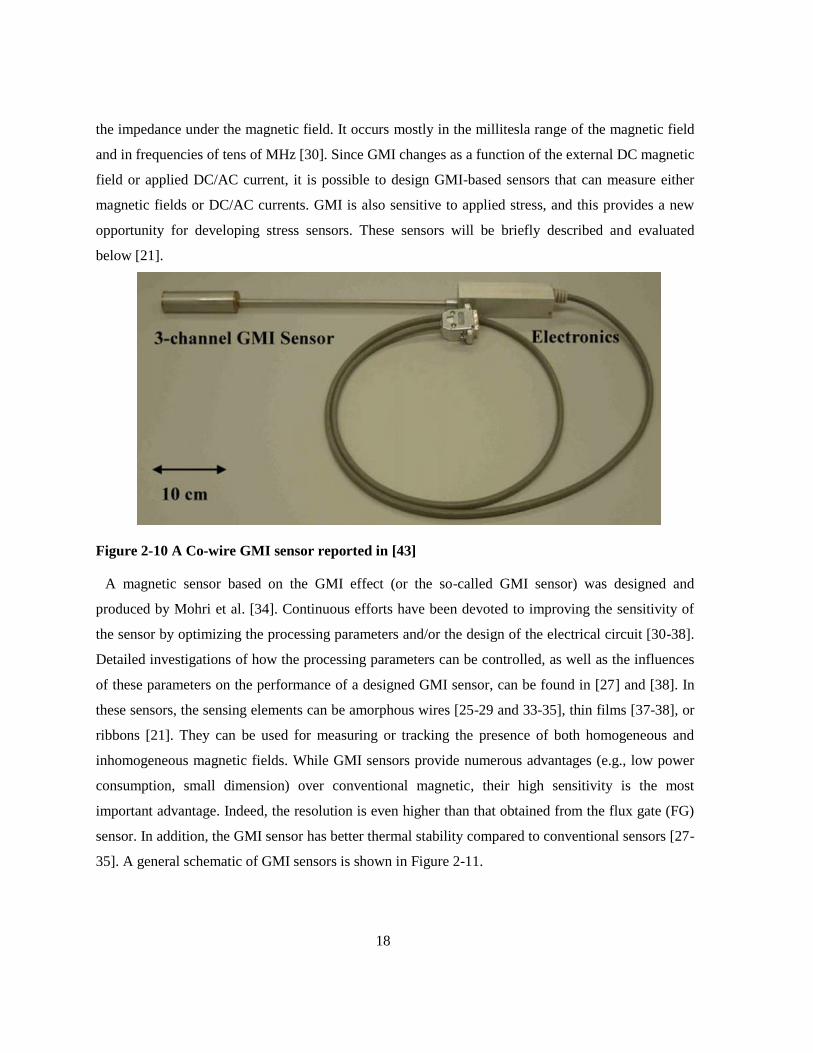
researchers, during which GMI was employed in wires and single thin films [25-38, 43]. Figure 2-10
shows an example of these sensors [43]. As we can see from the picture, the bulky nature of these
sensors makes them unfavorable for miniature applications. Although some researchers did attempt to
make multilayer GMI devices as well [33], [37], [38], the basic thrust of the GMI effect is to change
18
the impedance under the magnetic field. It occurs mostly in the millitesla range of the magnetic field
and in frequencies of tens of MHz [30]. Since GMI changes as a function of the external DC magnetic
field or applied DC/AC current, it is possible to design GMI-based sensors that can measure either
magnetic fields or DC/AC currents. GMI is also sensitive to applied stress, and this provides a new
opportunity for developing stress sensors. These sensors will be briefly described and evaluated
below [21].
Figure 2-10 A Co-wire GMI sensor reported in [43]
A magnetic sensor based on the GMI effect (or the so-called GMI sensor) was designed and
produced by Mohri et al. [34]. Continuous efforts have been devoted to improving the sensitivity of
the sensor by optimizing the processing parameters and/or the design of the electrical circuit [30-38].
Detailed investigations of how the processing parameters can be controlled, as well as the influences
of these parameters on the performance of a designed GMI sensor, can be found in [27] and [38]. In
these sensors, the sensing elements can be amorphous wires [25-29 and 33-35], thin films [37-38], or
ribbons [21]. They can be used for measuring or tracking the presence of both homogeneous and
inhomogeneous magnetic fields. While GMI sensors provide numerous advantages (e.g., low power
consumption, small dimension) over conventional magnetic, their high sensitivity is the most
important advantage. Indeed, the resolution is even higher than that obtained from the flux gate (FG)
sensor. In addition, the GMI sensor has better thermal stability compared to conventional sensors [27-
35]. A general schematic of GMI sensors is shown in Figure 2-11.

19
In addition to GMI sensors designers, some researchers started to investigate applications of these
sensors in real life. In 2014, Li[50] offered a study of surface acoustic wave (SAW) GMI sensors.
Using the SAW element, they achieved a wireless GMI sensor.
Although there are many publications on GMI sensors, this field currently suffers from a lack of
material characterization and FEM simulations of this phenomenon. A few publications [47-49] on
simulation are attempting to solve GMI-related equations numerically for a GMI single ribbon. GMI-
related equations and analytical models are discussed in detail in Chapter 4.
Figure 2-11 Schematic view of GMI element (a) top view (b) cross sectional view [38].

20
3 Chapter Three
Multilayer MEMS Reed Sensors
3.1 Introduction
For portable electronics with battery operation, a passive switch is more favorable compared to an
active switch. The conventional reed switch is a typical passive switch, which includes a glass
package containing two metal reeds. The metal reeds can be actuated to make a contact using an
external magnetic field. When the external magnetic field is removed, a spring restores the reed to its
original position. This approach is ideal for applications where conserving battery power is critical, as
the device does not consume power in the off state [8-10].
For portable electronics applications such as cellular phones, hearing aids and laptops, further
miniaturization, higher shock resistance, and better integration of switches are desirable. The micro-
electromechanical (MEMS) magnetic switch can meet these requirements. It mimics the operations of
the reed switch, but is fabricated using microfabrication technology. Therefore, it can drastically
reduce the size of the device, lower the fabrication cost, and improve shock resistance [2-3].
In this chapter, a preliminary design for a nickel-based magnetic reed switch is introduced. The
design is fabricated in several dimensions and shapes, ranging in length from 100 to 500 microns and
in width from 20 to 80 microns.
Unfortunately, the fabricated micro switches with nickel beams failed during testing. There are two
main reasons for this failure. First, as nickel is sensitive to EKC solution, it was not possible to wet
release the nickel structures. All the attempts to wet release it failed, as the nickel was etched away
before the sacrificial layer (polyamide). Second, the dry release of the nickel beams was adversely
affected by the residual polyamide under the beams, which prevented switch electrical contact. Even
the mechanically actuated switches failed to show contact resistance.
In order to overcome these issues, we suggested and designed a new fabrication process consisting
of a tri-layer of Au-Ni-Au beams. The new beams allowed us to wet release the structure and achieve
successful MEMS switches. Using Electro-less plating (ELP) for both nickel and gold layers resulted
in only 4 masks for this 7-layer MEMS structure. The low number of masking and lithography steps
effectively improves the microfabrication quality.
A review of governing equation in magnetostatic MEMS is first conducted, after which the required
FEM equations are presented and solved using the finite element software, COMSOL 4.2. By
utilizing COMSOL’s built-in modules for magnetostatic physics, the nickel switch is fully simulated

21
and the resulting magnetic force is determined for numerous system configurations. Next, mask
designing steps are reported and a quick review of fabrication process is done, including brief
descriptions of each step of the fabrication. Then, the challenges of these switch/sensors are discussed
and the tri-layer MEMS Reed sensors are introduced in the same order as the preceding. Finally, an
experimental setup for measurement is presented, along with the results and conclusion. Any
perceived errors and problems are listed here, as along with further improvements and suggestions to
overcome the challenges.
3.1.1 Theory
A physical-level analysis of magnetostatic MEMS requires a self-consistent solution of the coupled
mechanical and magnetic equations.. The basic reed switch consists of two ferromagnetic nickel-iron
beams encapsulated in glass. The two reeds act as magnetic flux conductors when exposed to an
external magnetic field from either a permanent magnet or an electromagnetic coil. Poles of opposite
polarity are created at the contact gap, with the contacts closing when the magnetic force exceeds the
spring force of the reeds. The contacts open when the external magnetic field is reduced so that the
magnetic attractive force between the reeds is less than the restoring spring force of the reeds.
The basic reed switch is a Single Pole Single Throw Normally Open (SPST-NO) switch. By
including an additional nonmagnetic contact that is electrically closed with no magnetic field present,
a Single Pole Double Throw (SPDT) switch (also known as a changeover switch) can be made. This
is a break-before-make switch, in that the closed contact opens before the open contact closes.
Generally, in MEMS magnetic reed switches, the goal is to make contact between the beams by the
force generated to maintain magnetic flux continuity. The magnetic flux is confined to the permanent
magnet and switch beams due to their high magnetic permeability. As the magnetic flux and magnetic
field require continuity, a force will be generated to lower the gap between the two beams and enable
contact.
The magnetic field gives rise to a magnetostatic body force which deforms the cantilever beam from
its initial position. When the beam deforms, the magnetic field changes, and the resultant
magnetostatic force and beam deformations also change. Figure 3-1(b) shows the deformation of the
cantilever at any given point in time and the forces acting on it. The magnetostatic force causes the

22
beams to deform to a state where they are balanced by internal stiffness; at that time, the inertial
forces are instantaneous (see Figure 3-1(b)).
Figure 3-1 Schematic view of undeformed magnetic switch and a deformed one [8].
The mechanical restoring force arises due to the stiffness of the structure and depends on the
displacement of the beam/structure at that instant in time, whereas the inertial force depends on beam
acceleration. The governing equations for each of the energy domains and their Lagrangian
formulations are discussed below. For details on the theory deployed in this thesis, please refer to [8]
and Appendix A.
Based on this approach, magnetostatic governing equations are derived from Maxwell’s equations.
Equations 1 and 2 show the derived magnetostatic equations.
𝑩 = 𝐵𝑋
𝐵𝑌 = 𝑭−𝑻
𝜕𝐴𝑧𝜕𝑌
−𝜕𝐴𝑧𝜕𝑋
= [1 +
𝜕𝑢
𝜕𝑋
𝜕𝑢
𝜕𝑌𝜕𝑣
𝜕𝑋𝟏 +
𝜕𝑣
𝜕𝑌
]
−𝑻
𝜕𝐴𝑧𝜕𝑌
−𝜕𝐴𝑧𝜕𝑋
(1)
𝒇𝒎𝒂𝒈 = 𝑴.𝜵𝒙𝑩 = 𝑴.𝑭−𝑻𝜵𝑿𝑩 (2)
where A is the magnetic field’s potential vector, F is the deformation gradient tensor, and M is the
magnetization vector. Equation 2 represents the magnetostatic body force acting on the microstructure
in the deformed configuration.

23
In a mechanical resorting force, one can calculate the spring constant of the beams based on
mechanical strength equations and beam dimensions. There are different equations for different kinds
of beams. For instance, for a simple cantilever beam, the spring constant is:
𝐾 =3𝐸𝐼
𝐿3
(3)
where E is the Young’s modulus of the beam material, L is beam length, and I is the moment of
inertia of the corresponding beam. A cantilever beam can be calculated by (31):
𝐼 =𝑤𝑡3
12
(4)
where w is beam width and t is beam thickness. After calculating the spring constant of the beam, the
mechanical restoring force can be calculated using Hooks law:
Fmech = ky (5)
Once the magnetic body force fmag is sufficiently high to overcome the Fmech value in the y=gap,
the switch will be actuated. It should be noted that more complicated beam models can be employed
to calculate mechanical forces, but response errors are negligible between various models. It is also
important to note that the spring constant equation will change by varying the beam and support
shapes. The above-mentioned equations are governing equations for magnetic reed switches/sensors,
which will be solved by finite element software. We have employed COMSOL multiphysics to solve
these equations and simulate the design. These results are discussed in the next sections.
3.2 Nickel-based Magnetic MEMS Reed Sensors
A magnetic MEMS reed switch/sensor is designed and fabricated on silicon. The reeds are
multilayer nickel beams with dimensions of 300*60 microns. Several types of switches with different
configurations have been designed and successfully fabricated, and a FEM COMSOL 4.2 simulation
is implemented to simulate the switch/sensor. Based on the simulation results, a magnetic body force
of 3.75µN is achieved at a 10 mT magnetic field. This force exceeds what is required to actuate the
switch. The switches have been tested in the lab under a constant magnetic field.
3.2.1 Modeling and FEM Simulation
In order to conduct a simulation of the magnetic reed switches/sensors, COMSOL Multiphysics 4.2a
is employed. Using COMSOL’s built-in physics (AC/DC module and structural mechanics), all of

24
the above equations have been solved. As well, a beneficial new feature of the AC/DC module is
magnetostatic force calculation, which makes simulation more straightforward for our case study.
As mentioned in the Introduction, we chose nickel as our beam material. Nickel’s permeability is
400, meaning it is a good ferromagnetic material that is less prone to oxidization than iron. Also,
nickel is conductive, so the beam itself can make electrical contact.
Because the MEMS switches are fabricated on wafers, the bottom electrode is fixed to the substrate
(first-level layer) and cannot have any movement and displacement. Therefore, the only moving part
in our design is the upper beam. Using the simulation results, and based on fabrication restrictions,
the bottom electrode thickness is chosen to be 3 microns. The resultant thickness of the upper beam is
then investigated for 3 microns and 1 micron. Based on the results in step 1, the micron thickness
beam has more magnetic body force and also has less mechanical restoring force due to being thinner.
The gap in our design is assumed to be 1 micron, but larger gaps have also been studied.
The beam lengths in the simulation portion of our work are assumed to be 100 microns, with a 50-
micron overlapping length between the two beams. The gap is assumed to be 1 micron. A permanent
magnet with different magnetization vectors has been placed in various positions and distances with
respect to the switch. Finally, the magnetic body force calculated in the AC/DC module is coupled to
a structural mechanic module, as the load and movement of the beam is investigated.
A brief review of simulation steps, along with the results of each step, is discussed and shown
below:
A) Choosing the physics
As our first step, a 2D analysis system was chosen in COMSOL, after which a model navigator
window, the AC/DC module, was selected. In the AC/DC module, we used magnetostatic fields with
no current. Later on, we will add Plane strain analysis from a structural mechanics module. By
selecting stationary analysis as our solving method, we proceed to the design portion in a GUI
window.
B) Drawing system in GUI
The second step is drawing the model in the model builder wizard. Objects of the system are
sketched as follows:

25
A large square of 2*2 mm is sketched and its boundary restricted to be magnetically insulated. This
large square is assumed to be our working environment with the whole system within it. The material
of this object is defined to be air. From henceforth in this report, we will refer to it as the
‘environment’.
A 20*25 µm rectangle is drawn as a permanent magnet within the environment, with a corner
(130µm, 50µm) in a Cartesian plane. From this point onward, we will refer to it as a ‘permanent
magnet’.
The upper beam is sketched with a 1-micron thickness, a 100-micron length, and a corner of (0,0).
The bottom electrode is then sketched with a 3-micron thickness, 100 micron-length, and a corner of
(-4µm, 48µm).
The gap in our design is assumed to be 1 micron, but larger gaps have been also studied. Figure 3- 2
shows the modeled structure in GUI.
Figure 3-2 Modeled magnetic MEMS switch in COMSOL 4.2 GUI.
C) Subdomain settings

26
In our subdomain settings, the material properties of each object have been defined and their
properties regarding magnetic calculation are clarified as follows.
Environment is defined as air, with µr = 1.
A permanent magnet is assumed to be magnetized iron with µr = 4000. The
magnetization vector of a magnet is assumed to be (20000,0) A/m. Other directions and
values of magnetization have also been studied.
Two beams are defined as nickel with µr = 400. The Young’s modulus of nickel is
defined as 180 GPa.
In the environment and two beams, the magnetic field is calculated as B = µ0µrH. In the permanent
magnet, the magnetized vector is defined by B = µ0(M + H).
D) Boundary settings
All boundaries are assumed to have magnetic continuity except for environment boundaries, which
are defined as magnetically insulated.
For mechanical boundaries, a bottom electrode and permanent magnet are fixed in place to preclude
any movement of these two objects. The upper beam is fixed at one side as x=0, and the other
boundaries are defined as being free to move. The body force generated by the magnetic flux is
assumed to apply to the tip of the upper beam.
E) Mesh settings
As we do not have any preferred shape of meshing, we chose the free triangle meshing method.
However, due to the small gap and small feature size of beams with respect to the rest of the objects,
the meshing is refined for these areas. Thus, we have an increased number of elements in critical parts
to obtain more accurate answers from our simulation.

27
Figure 3-3 Meshing of modeled magnetic MEMS switch.
A) Magnetic force calculation
A recently added feature to COMSOL 4.2a is the magnetostatic force calculation option. This
feature will solve the mentioned equations in the theory section for the system and calculate the
magnetic body force for each of the desired objects. In our case, an upper beam is selected to
ascertain the magnetic body force on it. Note that this body force is a vector, so its sign and
components will determine its direction.
In our simulation, we achieve magnetic forces as high as -3 µN at 10mT magnetic field between the
two. In our case, using the given dimensions of the upper beam, we need about 0.3 µN of magnetic
force to overcome the mechanical restoring force. Thus, the generated body force is sufficiently far to
actuate the system.
Case study a)
M= (0, 20000)
Permanent magnet corner= (130, 50) microns
The simulated plot is shown below. Here we can see the magnetic flux density and the contour plot
of the magnetic flux in Figures 3-5 and 3-6, respectively.

28
Figure 3-4 Shows the magnetic flux density in Tesla for case a).
As is clear in Figure 3-6, the maximum flux in between and around the magnetic switch is 0.012 T,
which is the actuation needed field with this configuration. Moreover, the achieved force here is -3.2
µN, which far exceeds the required force for switch actuation. The shape of magnetic flux contours
are shown in Figure 3-5.

29
Figure 3-5 Shows magnetic flux density contours for magnetic switches.
As can be seen in the above figure, the magnetic field lines are trying to connect to each other and
maintain continuity. This is the reason for the force generation, which will make the flux continuity
easier. Figure 3-6 shows the magnetic flux streamline between two beams to better clarify this
phenomenon.

30
Figure 3-6 Magnetic flux density streamlines between the beams for case a).
Figure 3-7 shows the position of the system in the environment.
Figure 3-7 Whole magnetic model of the switches in the environment.
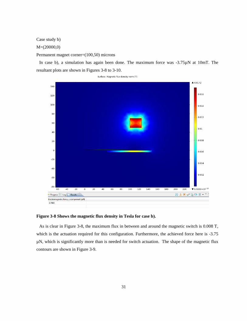
31
Case study b)
M=(20000,0)
Permanent magnet corner=(100,50) microns
In case b), a simulation has again been done. The maximum force was -3.75µN at 10mT. The
resultant plots are shown in Figures 3-8 to 3-10.
Figure 3-8 Shows the magnetic flux density in Tesla for case b).
As is clear in Figure 3-8, the maximum flux in between and around the magnetic switch is 0.008 T,
which is the actuation required for this configuration. Furthermore, the achieved force here is -3.75
µN, which is significantly more than is needed for switch actuation. The shape of the magnetic flux
contours are shown in Figure 3-9.

32
Figure 3-9 Magnetic flux density contours for case b).
Figure 3-10 Magnetic flux density streamlines between the beams for case b).

33
In the future, research should focus on investigating the working positions of the permanent magnet
around the switches in order to ascertain the graph of actuation position for the switches.
Assuming that we have this body force as the load in the structural mechanic module, we can see
the actuation of the switch, as below.
Figure 3-11 Actuation of switch at 10 mT.
As can be seen in the figure’s legend, the displacement is expected to be much higher than a 1-
micron gap. The upper beam will make contact with the lower one and will not go any further. Hence,
the plot has been rescaled to show a correct answer.
3.2.2 Design and Mask-Making
The thickness of the beams is determined according to simulation results. A minimum length of 100
µm has been shown to work well within the designated conditions. Increasing the length will reduce
the spring constant, making actuation of the devices easier. In the design step, several types of
switches/sensors have been developed, each with three different lengths (500, 400 and 300) µm and

34
three different widths (40, 60 and 80) µm. Excluding the size differences, the designs can be
categorized into five types:
Switches with simple cantilever beam and simple fixed supports (type 1).
Switches with minder hinge cantilevers; the support has a minder shape with two
connection widths of 15 microns each. Using minder shape supports greatly reduces the
spring constant of the beam, which makes actuation easier and less forceful, thus lowering the
magnetic field (type 2).
Switches with simple cantilever beam and simple fixed supports, with a 20-micron
width but a wider tip of 60 microns (type 3).
Two-way arrays of switches with widths of 60 microns, designed in all three lengths.
Two arrays are perpendicular to each other and are of equal length. This design will help in
sensing the direction of the magnetic field (type 4).
Four-way arrays of switches. This is a multi-output switch with 4 outputs of various lengths.
It can be used to actuate systems that require different amounts of sensitivity to magnetic fields
(type 5).
Each layer of the four-layer mask is described below.
Layer 1 is a light field mask for patterning the bottom electrodes and conductive pads
for the test. This layer will be masked with positive photoresist.
Layer 2 is a light field mask for patterning the anchor. It will be patterned with
negative photoresist.
Layer 3 is a dark field mask for dimples. It is patterned with positive photoresist.
Layer 4 is also dark field, but it is for patterning upper beams using negative
photoresist.

35
Table 3-1 Lithography mask layers
Table 3-2 Layer Names, Thicknesses, and Mask Levels
Figure 3-12 shows the final 4-layer mask in a single view (note: small features may not be visible).
The design rules, which include all the physical limitations and fabrication process limitations that
have been considered in the mask design process, are discussed in detail in Appendix B.

36
Figure 3-12 Final mask printed on glass.
3.2.3 Fabrication Process
The fabrication is carried out on four 4-inch silicon wafers. Following the RCA cleaning of the
wafer, a 0.5 micron of PECVD silicon oxide is deposited on three of the wafers, and a 0.5-micron of
PECVD silicon nitride is deposited on the last one. This dielectric deposition has been done to ensure
that the substrate is fully insulated.
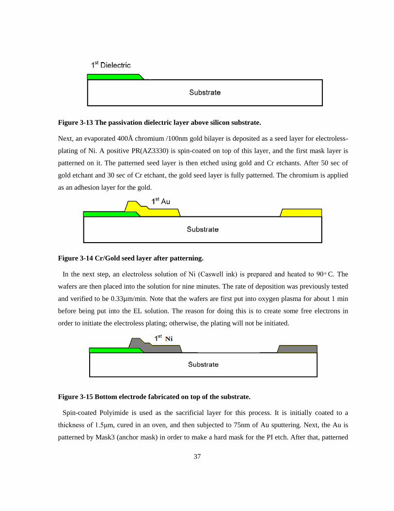
37
Figure 3-13 The passivation dielectric layer above silicon substrate.
Next, an evaporated 400Å chromium /100nm gold bilayer is deposited as a seed layer for electroless-
plating of Ni. A positive PR(AZ3330) is spin-coated on top of this layer, and the first mask layer is
patterned on it. The patterned seed layer is then etched using gold and Cr etchants. After 50 sec of
gold etchant and 30 sec of Cr etchant, the gold seed layer is fully patterned. The chromium is applied
as an adhesion layer for the gold.
Figure 3-14 Cr/Gold seed layer after patterning.
In the next step, an electroless solution of Ni (Caswell ink) is prepared and heated to 90 C. The
wafers are then placed into the solution for nine minutes. The rate of deposition was previously tested
and verified to be 0.33µm/min. Note that the wafers are first put into oxygen plasma for about 1 min
before being put into the EL solution. The reason for doing this is to create some free electrons in
order to initiate the electroless plating; otherwise, the plating will not be initiated.
Figure 3-15 Bottom electrode fabricated on top of the substrate.
Spin-coated Polyimide is used as the sacrificial layer for this process. It is initially coated to a
thickness of 1.5μm, cured in an oven, and then subjected to 75nm of Au sputtering. Next, the Au is
patterned by Mask3 (anchor mask) in order to make a hard mask for the PI etch. After that, patterned

38
gold is used as a mask for PI, and the anchor is etched using the EKC wet etch of PI to fully clear the
anchor holes.
Figure 3-16 Patterned anchor (the gold layer on top of PI is not shown to prevent
misunderstanding).
Following the patterning procedure, AZ330 is again used to pattern the anchor dimple mask by
removing the gold layer in the gold etchant. The wafers are then placed in RIE to remove dimples
with 1-micron thickness. After patterning dimples on the PI, the covering gold layer is removed using
a gold etchant. The resultant state is shown in Figure 3-17.
Figure 3-17 Wafer after patterning anchor and dimples on PI.
Afterward, the wafers are sputtered in 50 nm of gold and the final layer is patterned on the gold
using NLOF2550. Then the same process that was done for the first EL plating is repeated in order to
create upper nickel beams. The final structure, prior to release, is shown in Figure 3-18.
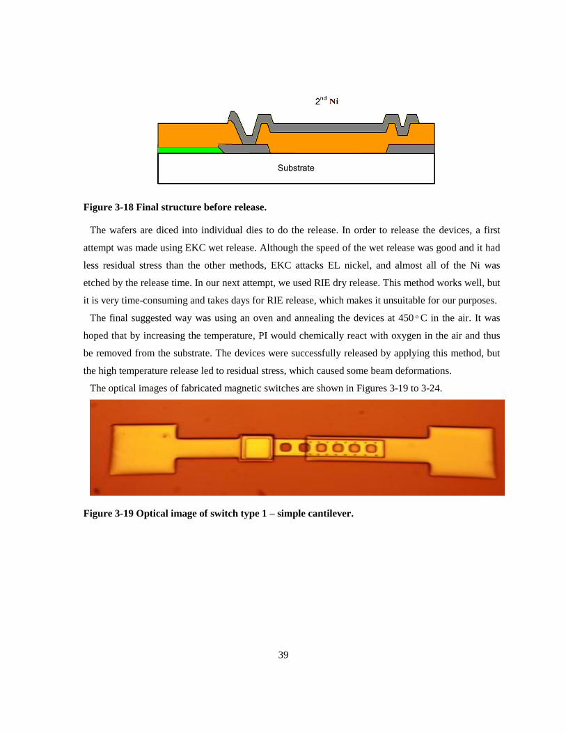
39
Figure 3-18 Final structure before release.
The wafers are diced into individual dies to do the release. In order to release the devices, a first
attempt was made using EKC wet release. Although the speed of the wet release was good and it had
less residual stress than the other methods, EKC attacks EL nickel, and almost all of the Ni was
etched by the release time. In our next attempt, we used RIE dry release. This method works well, but
it is very time-consuming and takes days for RIE release, which makes it unsuitable for our purposes.
The final suggested way was using an oven and annealing the devices at 450 C in the air. It was
hoped that by increasing the temperature, PI would chemically react with oxygen in the air and thus
be removed from the substrate. The devices were successfully released by applying this method, but
the high temperature release led to residual stress, which caused some beam deformations.
The optical images of fabricated magnetic switches are shown in Figures 3-19 to 3-24.
Figure 3-19 Optical image of switch type 1 – simple cantilever.
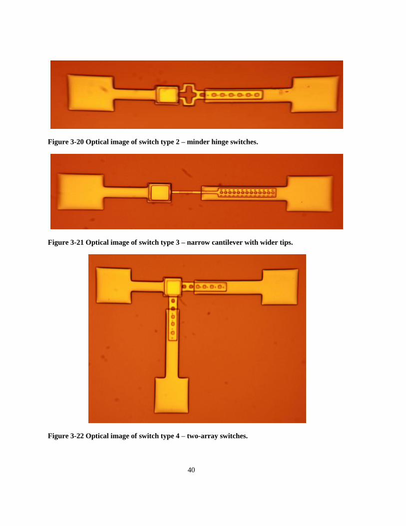
40
Figure 3-20 Optical image of switch type 2 – minder hinge switches.
Figure 3-21 Optical image of switch type 3 – narrow cantilever with wider tips.
Figure 3-22 Optical image of switch type 4 – two-array switches.

41
Figure 3-23 Optical image of switch type 4 – four-arrays switches.
Figure 3-24 Optical image of tip of one cantilever showing the position of the upper beam with
respect to the lower one; dimples and release holes are shown here.

42
Figures 3-25 to 3-29 illustrate some SEM images of fabricated devices. The quality of the
fabrication is clear in these figures.
Figure 3-25 Magnetic Reed SW- a) minder shape support SW – width 60um and length 380 um
b)SW – width 80um and length 400 um.

43
Figure 3-26 An Array of 2 Magnetic Reed SW – width 60um and length 370 um.

44
Figure 3-27 An Array of 2 Magnetic Reed SW – width 60um and length 370 um (side view).
Figure 3-28 Magnetic Reed SW type 2 – width 60um and length 270 um.

45
Figure 3-29 Magnetic Reed SW with wide tip type 3 – width (w1: 20um, w2:60um) and length
500um.
3.2.4 Experimental Setup and Measurements
In order to do the measurements, an experimental set up is prepared, which consists of:
Helmholtz coil
Custom-made stage
DC Probes
Microscope
Permanent magnets of various field strength
A custom-built stage, fabricated in the machine shop, takes the measurements. The stage stands at the
middle height of the coil, and its opening can be controlled in order to accept various dies of devices.
The entire stage is made of aluminum, which will not affect the magnetic field in our measurements.
A photo of the fabrication setup is shown in Figure 3-30.

46
Figure 3-30 Photo of measurement setup and stage.
As shown above, a high magnification microscope is employed in this setup. The microscope has a
small lens, so it can be placed directly above the sample. The picture is shown in the monitor
connected to the microscope. In this study, measurements are done simply to test if the switches are
actuated or not. In order to test this, a multimeter is used to measure the contact resistance of the line.
In an unactuated switch, the resistance should be infinite and the multimeter should not show us
anything. However, as soon as the switch is actuated and contact occurs, the multimeter should show
some resistance, which is related to the contact resistance of the switch.
In the first set of fabricated switches, no results occurred using this method. Even the upper beam
was actuated mechanically by a microprobe, and no contact resistance was observed. The problem is
caused by the imperfect release of the device. Most likely, some photoresist remains underneath the
upper beam, which will isolate the upper beam from the lower one. In order to solve this problem, a
new fabrication process is attempted, as discussed section 3.3.
3.3 Tri-layer Magnetic MEMS Reed Sensors
In order to overcome the fabrication problems of Ni-based MEMS sensors, we use a tri-layer of
Au/Ni/Au magnetic MEMS reed switch/sensors, designed and fabricated on silicon. The reeds are
multilayer nickel beams covered with gold, with dimensions of 300*60 microns. Several types of
switches with different configurations are designed and successfully fabricated. A 2D and 3D FEM
COMSOL 4.2 simulation is implemented to simulate the switch/sensor. Based on simulation results, a
magnetic body force of 5 µN is achieved in a 10 mT magnetic field. This force is more than is

47
required to actuate the switch. The switches are tested in the lab under a constant magnetic field, and
the test results discussed at the end of this section.
3.3.1 Modeling and FEM Simulation
COMSOL Multiphysics 4.2 is employed to simulate the tri-layer MEMS sensors. Using COMSOL
built-in physics (AC/DC module and structural mechanics) the magnetic physics is coupled to te
mechanical force and displacement.
As in the previous section, the MEMS switches are fabricated on wafers. The bottom electrode is
fixed to the substrate (first-level layer) and cannot have any movement and displacement. Therefore,
the only moving part in our design is the upper beam. Using the simulation results, and based on
fabrication restrictions, we chose the bottom electrode thickness to be 4 microns. The resultant
thickness of the upper beam is investigated for 3 microns and 1.2 micron. Based on the results in step
1, the micron thickness beam shows more magnetic body force and has less mechanical restoring
force due to being thinner. The gap in our design is assumed to be 1 micron, but larger gaps have also
been studied. In order to maximize the actuation force and also reduce the effect of gold on the
mechanical performance of switches, the gold thickness was chosen to be 100 nm in thickness.
The beam lengths in the simulation portion of our work are assumed to be 100 microns, with a 50-
micron overlapping length between the two beams. The gap is assumed to be 1 micron. A permanent
magnet with different magnetization vectors has been placed in various positions and distances with
respect to the switch. Finally, the magnetic body force calculated in the AC/DC module is coupled to
a structural mechanic module, and the beam’s load and movement are investigated.
3.3.1.1 2D FEM simulation
A brief review of simulation steps, along with the results of each step, is discussed and shown
below:
A) Choosing the physics
As our first step, we chose a 2D analysis system in COMSOL, and then selected the AC/DC module
as a model navigator window. In the AC/DC module, we used magnetostatic fields with no current,

48
but later on added Plane strain analysis from a structural mechanics module. By selecting stationary
analysis as our solving method, we can proceed to the design portion in a GUI window.
B) Drawing system in GUI
The second step is drawing the model in the model builder wizard. Objects of the system are
sketched as follows:
A large square of 2*2 mm is sketched and its boundary restricted to be magnetically insulated. This
large square is assumed to be our working environment with the whole system within it. The material
of this object is defined as air. From this point onward, we will refer to it as the ‘environment’.
A 20*25 µm rectangle is drawn as a permanent magnet within the environment, with a corner of
(130µm, 50µm) in a Cartesian plane. From this point onward, we will refer to it as the ‘permanent
magnet’.
The upper beam is sketched with a 1-micron thickness, a 100-micron length, and a corner of (0,0).
The bottom electrode is then sketched with a 3-micron thickness, a 100 micron-length, and a corner
of (-4µm, 48µm).
The gap in our design is assumed to be 1 micron, but larger gaps have been also studied. Figure 3-
31 a-c shows the modeled structure in GUI for the case of without packaging, with glass packaging,
and gold beams with nickel tips with packaging.

49
Figure 3-31- The COMSOL geometry 2D sketch of MEMS read switches, for a a)tri-layer
without packaging, b) tri-layer with glass packaging and c) nickel tip gold beams with the
packaging
By implementing the simulations in these conditions, we see that glass packaging and gold cover do
not have much of an effect on device performance. The reason for this is that the H field passes
through all non-magnetic material and does not see them in the way. Hence, they cannot have any
effect on the H field interaction with a magnetic material.

50
Figure 3-32 the 2D COMSOL simulation for a tri-layer MEMS without packaging, this
graph illustrates the vertical displacement of sensors beams in actuated condition (10 mT
magnetic field). As shown above, the upper beam is experiencing a 4 um downward
displacement which is 4 times greater than our 1 um designed gap.

51
As shown in Figure 3-35, the tri-layer MEMS sensor shows promising behavior in the desired
magnetic field. The packaged sensors are discussed in greater detail in order to fully study the case in
a real environment. In the study, the actuator permanent magnet is swept in the X, Y and Z directions.
The performance map of the device is concluded and sketched using the results of this step. The
schematic geometry of the full model sensor with packaging is shown in Figure 3-34 b. Figures 3-36
to 3-37 show the coupled simulation of the full model sensors.
Figure 3-33 Surface plot of magnetic field on Tri-layer MEMS Reed switch with packaging, as
shown above, the sensing magnetic field for the actuation is 9-11 mT.
As shown in Figure 3-36 the sensing magnetic field for the sensor actuation is around 10 mT. The
surface plot of upper beam displacement and magnified projected out of place displacement of both
beams are illustrated in Figures 3-37 and 3-28, respectively.
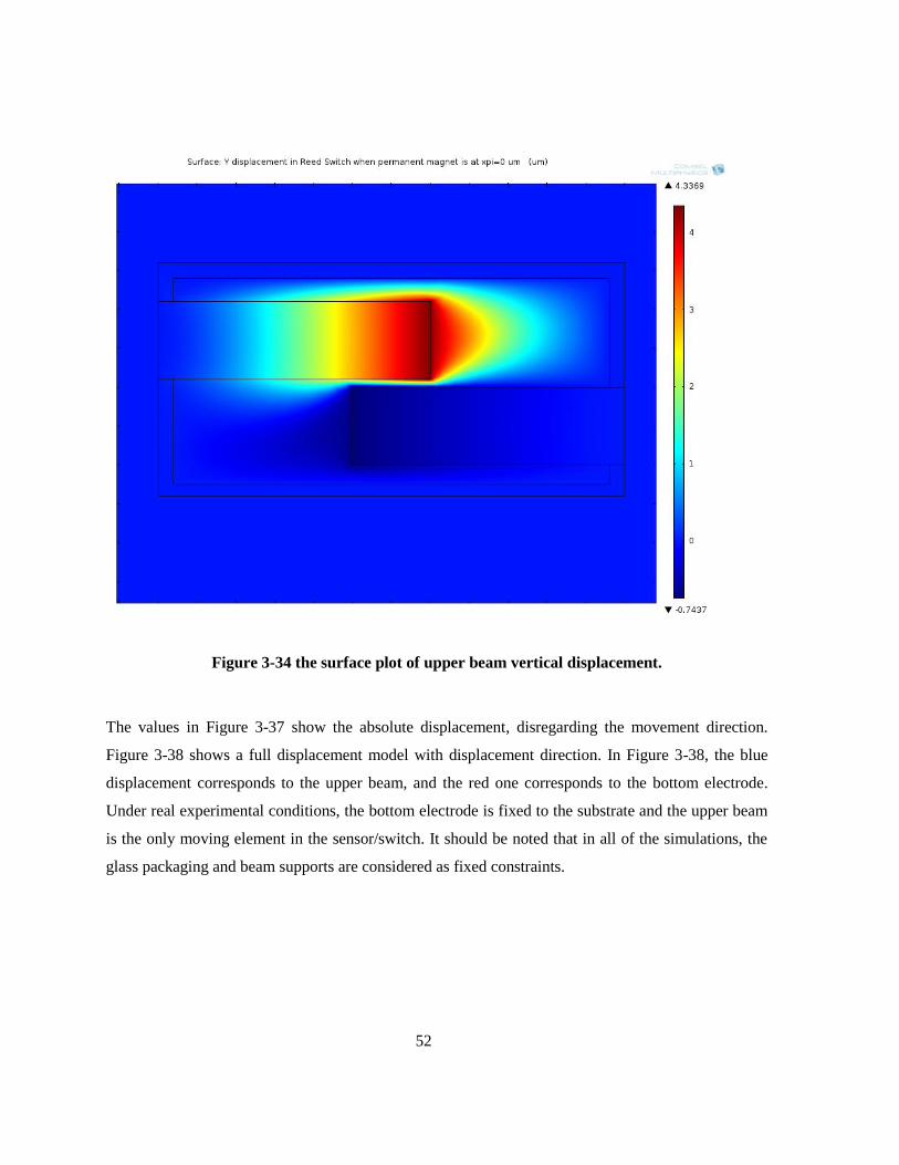
52
Figure 3-34 the surface plot of upper beam vertical displacement.
The values in Figure 3-37 show the absolute displacement, disregarding the movement direction.
Figure 3-38 shows a full displacement model with displacement direction. In Figure 3-38, the blue
displacement corresponds to the upper beam, and the red one corresponds to the bottom electrode.
Under real experimental conditions, the bottom electrode is fixed to the substrate and the upper beam
is the only moving element in the sensor/switch. It should be noted that in all of the simulations, the
glass packaging and beam supports are considered as fixed constraints.

53
Figure 3-35 magnified projected out of place displacement of both beams. The blue color is
corresponded to upper beam with the downward movement whereas the red on is corresponded
to the upward movement of the bottom electrode
3.3.1.2 3D simulation of the MEMS Sensors
To finalize the full model simulation a 3D simulation is implemented on the same sensor with the
same dimensions and materials. The results are shown below.

54
In the simulation, the magnetostatic physic from AC/DC module is coupled to mechanical body force
calculations. Thus, the total generated force on the upper beam can be tracked while the permanent
magnet is sweeping in different direction. To get a 2D surface plot of the simulations, slicers are
added in a post-processing module. The general solution of the simulation is presented in Figure 3-37.
Figure 3-38 shows the generated force on the upper beam when moving the permanent magnet in the
X direction.
Figure 3-36 Simulation setup and 3D geometric design of MEMS read sensors.

55
Figure 3-37 Magnetic field distribution over sensor in an actuation step.

56
Figure 3-38 Generated force eon the upper beam. In the positions with negative value the
actuation will happen. In this figure x axis represents x direction and the unit is micro meter.
3.3.1.3 Performance Map of Sensors
The working map of the sensors is achieved by moving the permanent magnet in X, Y, and Z
directions. The generated forces are tracked in different positions and the one conducting to an
actuation is picked. A summary of these results is presented in Figure 3-42. Note that this figure
illustrates the general trend, and that the values will change based on the magnetic field of the
permanent magnet and the size of the sensor beams. In Figure 3-39, the state in which the generated
magnetic force is higher (with consideration of a safety factor) than the required mechanical force to
actuate the switch is the CLOSED position. This region will always demonstrate the actuated
sensor/switch condition. In the same figure, OPEN is the unactuated state of the switch, which
contains regions with small generated magnetic force that cannot actuate the switch. Finally, HOLD
is the distance range in which the generated magnetic force is in the same order as the required
mechanical force. The sensor/switch in this region maintains the state of its previous region.
Therefore, when sweeping from a CLOSED state to this region, the sensor/switch will maintain the
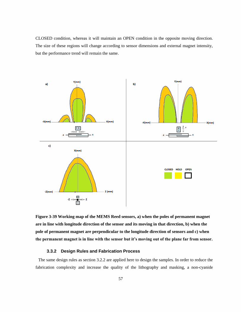
57
CLOSED condition, whereas it will maintain an OPEN condition in the opposite moving direction.
The size of these regions will change according to sensor dimensions and external magnet intensity,
but the performance trend will remain the same.
Figure 3-39 Working map of the MEMS Reed sensors, a) when the poles of permanent magnet
are in line with longitude direction of the sensor and its moving in that direction, b) when the
pole of permanent magnet are perpendicular to the longitude direction of sensors and c) when
the permanent magnet is in line with the sensor but it’s moving out of the plane far from sensor.
3.3.2 Design Rules and Fabrication Process
The same design rules as section 3.2.2 are applied here to design the samples. In order to reduce the
fabrication complexity and increase the quality of the lithography and masking, a non-cyanide

58
Electroless plating (ELP) of gold is employed here. The ELP layer forms over the top of the copper
and nickel. As the base layer here is nickel, ELP gold was successfully used to cover the nickel
layers. Using ELP reduces the masking and lithography steps. Hence, in the 7-layer microfabrication
of this work, only 4 masks are used, as reported in section 3.2.2.
The fabrication is carried out on three 4-inch silicon wafers. After the RCA cleaning of the wafer, a
0.5 micron of PECVD silicon oxide is deposited on three of the wafers (step a). This dielectric
deposition has been done to ensure that the substrate is fully insulated. As the fabrication steps are
similar to section 3.2.3, all steps are summarized in Figure 3-43, and the extra steps are discussed.
Figure 3-40 Fabrication steps of trilayer MEMS Reed switches
As shown in Figure 3-43, following Step A, a seed layer of Cr (50 nm)/Au (100nm) is deposited on
the substrate. The Cr layer serves as an adhesive between the gold and the oxide (step b). In Step B,
the first masks are patterned on the substrate using positive photoresist, after which the extra Cr/Au is
wet-etched. Next, in Step C, 3 micro meters of nickel are electroless plated on top of the gold. Similar
to section 3.2.3, the gold layers had to be agitated with oxygen plasma RIE before plating. The

59
substrate is then dipped into a gold ELP solution to form 100 nm of gold on top of the nickel.
Afterwards, polyimide is spin-coated as the sacrificial layer and cured in the oven at 330 C for 2
hours. After curing the polyamide, mask 2 (anchors) is patterned, followed by dry etching of the PI
layer in RIE. Similarly, mask 3 (dimples) is dry etched in RIE. Finally, the upper beam is fabricated
on top using the same steps as the bottom electrode. The only difference is that, after deposition of the
gold seed layer, the final mask (mask 4) is patterned on it. Detailed fabrication steps with parameters
are reported in Appendix C. The wafers are diced into individual die to ensure their release. EKC wet
release is used to release the devices. As the nickel layers are covered by gold so they will not be
damaged by EKC. After 15 minutes of release in EKC at 60 C, the dice are moved and dipped 3
times in IPA, each time for 15 minutes. At the end of third IPA dipping the dice are moved to the Co2
critical dryer to prevent stiction. Figures 3-44 to 3-46 show the optical microscopic images of various
devices made in this stage.

60
Figure 3-41 Optical microscopic image of trilayer MEMS Reed sensors a)

61
Figure 3-42 Optical microscopic image of trilayer MEMS Reed sensors b)

62
Figure 3-43 Optical microscopic image of trilayer MEMS Reed sensors c)
3.3.3 Test and Experiment
In order to do the measurements, an experimental set up is prepared, which consists of:
Helmholtz coil
Custom-made stage
DC Probes
Microscope
Permanent magnets of various field strength
A custom-built stage, fabricated in the machine shop, will do the measurements. The stage will
stand at the middle height of the coil, and its opening can be controlled in order to accept various dies
of devices. The entire stage is made of aluminum, which will not affect the magnetic field in our
measurements. As shown in Figure 3-33, a high magnification microscope is employed in this setup.

63
The microscope has a small lens, so it can be placed directly above the sample. The picture will be
shown in the monitor connected to the microscope. In this study, measurements are done simply to
test if the switches are actuated or not. In order to test this, a multimeter is used to measure the
contact resistance of the line. In an unactuated switch, the resistance should be infinite and the
multimeter should not show us anything. However, as soon as the switch is actuated and contact
occurs, the multimeter will show some resistance, which is related to the contact resistance of the
switch. The multimeter shows an open circuit in ‘off’ mode, but while we have 10 mT of magnetic
field, a contact resistance of 20 ohm is measured. Figure 3-47 illustrates a schematic summary of this
measurement.
Figure 3-44 Summary of MEMS reed sensor actuation test

64
4 Chapter Four
Giant Magneto-Impedance Thin film Magnetic Sensors
4.1 Introduction
Magnetic sensors play an essential role in modern technology. They are widely used in nearly all
engineering and industrial sectors, such as high-density magnetic recording, navigation, military and
security, target detection and tracking, antitheft systems, nondestructive testing, magnetic marking
and labelling, geomagnetic measurements, space research, measurements of magnetic fields onboard
spacecraft and biomagnetic measurements in the human body [16–20].
A magnetic sensor directly converts the magnetic field into a voltage or resistance with, at most, a
dc current supply, and the field sensitivity of a magnetic sensor plays a key role in determining its
operating regime and potential applications. For instance, SQUID gradiometers with a high sensitivity
of 10-10
–10-4
Oe have been used for measuring field gradients or differences due to permanent dipole
magnets in major applications of brain function mapping and magnetic anomaly detection. Induction,
fluxgate and GMR sensors with a medium sensitivity of 10-6
–102 Oe have been used for measuring
perturbations in the magnitudes and/or direction of Earth’s field due to induced or permanent dipoles
in major applications of magnetic compasses, munitions fuzing and mineral prospecting. Hall-Effect
sensors with a low sensitivity of 1–106 Oe have been used for applications of non-contact switching,
magnetic memory readout and current measurements. In addition to the sensitivity requirement, other
factors affecting the practical uses of magnetic sensors include processing cost and power
consumption. When comparing the processing costs and power consumption of existing magnetic
sensors, the GMR sensor shows the lowest cost and power consumption. However, the field
sensitivity of the GMR sensor is rather low (~1%/Oe).
Recently, the development of high-performance magnetic sensors has benefited from the discovery
of a new magnetic phenomenon – the giant magnetoimpedance (GMI) (i.e., a large change in the ac
impedance of a magnetic conductor with an ac current when subjected to an applied dc magnetic
field), in metal-based amorphous alloys [21[,[22]. It has been demonstrated that magnetic sensors
based upon the giant magnetoimpedance (GMI) effect offer several advantages over conventional
magnetic sensors. The decisive factor is the ultra-high sensitivity of GMI sensors. When compared
with a GMR sensor that has a sensitivity of ~1%/Oe, the field sensitivity of a typical GMI sensor can
reach a value as high as 500%/Oe [17],[20]. Though the development of GMI sensors is still at an

65
early stage, it is likely that their low prices and high flexibility will warrant wide-ranging application
in the near future.
Historically, GMI has attracted particular interest in the scientific community only since Panina and
Mohri for the first time announced their discovery of the so-called GMI effect in Co-based
amorphous wires in 1994 [15],[19]. In actual ferromagnetic materials, the maximum value of the GMI
effect experimentally obtained to date is much smaller than the theoretically predicted value [18].
Consequently, research in this field has focused mainly on special thermal treatments and/or on the
development of new materials for properties improvement [15],[24-34]. In order to design and
produce novel GMI sensors, a thorough understanding of the GMI phenomena and the properties of
GMI materials, with an emphasis on how a magnetic sensor utilising the GMI effect can be best
designed for technological applications, is indispensable. The next section aims to provide a
comprehensive analysis on the theory, design and fabrication of GMI Thin film magnetic sensor and
its potential applications.
4.2 Theory
Based on the frequency (f) of the driving ac, the giant magnetoimpedance can generally be
classified into the following frequency regimes:
(i) Low-frequency regime (up to a few kHz), where the changes in voltage at the sample’s ends are
mainly due to the so-called magnetoinductive effect [21]. The skin effect is very weak in this case.
The change in the impedance of the sample upon application of the applied field (Hdc) results mainly
from the contribution of inductance (L), which is proportional to the circumferential permeability (l/)
for a cylindrical magnetic conductor (i.e., a magnetic wire) or the transverse permeability (lT) for a
planar magnetic film (i.e., a magnetic ribbon) [21],[30].
(ii) Intermediate frequency regime (between _100 kHz and a few MHz), where GMI originates
mainly from the variation of the skin depth due to strong changes of the effective magnetic
permeability caused by the applied dc magnetic field. It is noted here that, depending on sample
geometry, the GMI profile can reach its peak in the intermediate frequency range (e.g., 100 kHz to 10
MHz), as a consequence of the contribution of the permeability from both domain wall motion and
magnetization rotation to GMI. Reduction in GMI at higher frequencies is related to the domain walls
becoming strongly damped by eddy currents and only magnetization rotation contributes to GMI.
(iii) High-frequency regime (several MHz up to GHz), where the origin of GMI is believed to be
related to the gyromagnetic effect and ferromagnetic relaxation. The maxima in GMI profiles are

66
shifted towards higher fields, where the samples are already saturated magnetically [21],[29],[34].
Strong changes in skin depth are caused by the same mechanism as in the ferromagnetic resonance.
There are theoretical various models of GMI representing each of the above-mentioned frequency
ranges. In this research, we employed and modified one famous and one generic model.
The advantageous features of the MI effect in a multilayer film can be illustrated by considering the
simplified three-layer structure shown in Fig. 4-1. A film of a width b (y-axis) and a length l (z-axis)
is composed of an inner conductive lead (M) of a thickness 2d1 and two outer ferromagnetic layers
(F) of a thickness d2. An AC current I = I0 exp(−jωt), flowing in the length direction mainly along
the conductive lead if its conductivity (σ1), is much larger than the conductivity of the ferromagnetic
layers (σ2). The F-layers are assumed to have a transverse in-plane magnetic anisotropy. A DC
magnetic field 𝐻𝑒𝑥 is applied parallel with the current. For 𝐻𝑒𝑥smaller than the anisotropy field 𝐻𝐾, a
transverse stripe exists as the main structure, as shown in Fig. 4-1b. Magnetic anisotropy is the
dependence of the magnetic properties on the direction of the applied field with respect to the crystal
lattice. It turns out that depending on the orientation of the field with respect to the crystal lattice one
would need a lower or higher magnetic field to reach the saturation magnetization. The effect of this
anisotropy field is studied further in chapter 5.
Figure 4-1 Schematic drawing of multilayer MI element, a) cross sectional view b)top view [37].
First, we consider a case where the film width, b, is sufficiently large and the edge effect can be
neglected [14], which is valid if b ≫ 2λ, λ2 = d1d2µt, µt is the transverse permeability. Within this

67
approximation, all of the variables depend on the thickness in the film (x) only. The permeability
tensor, µ, averaged over domains, has a quasi-diagonal form withµyz = µzy = 0. Maxwell’s equation
can be satisfied by considering the electric field (ez), and the magnetic field (hx, hy) with the
condition for the magnetic induction bx = 0, and the boundary condition hy(±d) = ±2πI
cb (d =
d1 + d2). The impedance can be written in a general analytical form as:
Z = Rf(x1, x2)(ξx1 + x2),
f(x1, x2) =coth x1 coth x2 + ξ
coth x1 + ξ coth x2 x1 =
(j − 1)d1
2δ1, x2 =
(j − 1)d2
δ2,
ξ2 =σ1µt
σ2, δ1
2 =c2
2πωσ1, δ2
2 =c2
2πωσ2µt .
(33)
Here, R is the DC resistance and will be defined by (34) µt = µyy + µyx2/µxx [31]:
R =l
2b(d1σ1 + d2σ2)
(34)
C is the velocity of light (Gaussian units are used). A low frequency (x1, x2 ≪ 1) expansion of
Equation (33) together with the condition d1σ1 ≫ d2σ2 yields a simple form for the impedance:
Z = Rm (1 − 2jµt
d2d1
δ12 ), Rm =
l
2bd1σ1.
(35)
In this approximation, the contribution of the magnetic layers to the sandwich impedance is
described by the external inductance with respect to the inner layer. For the sandwich of a submicron
thickness, this is a reasonable approach for frequencies up to several gigahertzes. It may be compared
with MI in a single magnetic layer in which a large magnetic response of Z is possible only in the
case of a strong skin effect (x2 ≫ 1), when Z ∝ 1 σ2⁄ ∝ √ωµt.
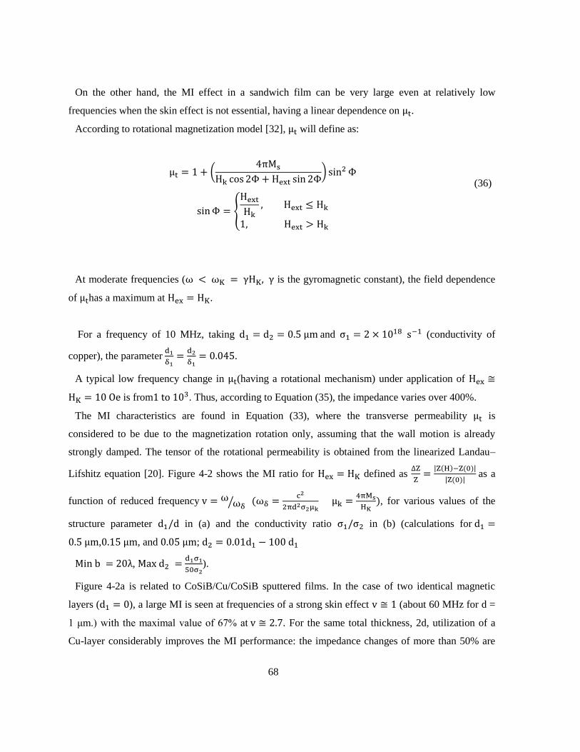
68
On the other hand, the MI effect in a sandwich film can be very large even at relatively low
frequencies when the skin effect is not essential, having a linear dependence on µt.
According to rotational magnetization model [32], µt will define as:
µt = 1 + (4πMs
Hk cos2Φ + Hext sin 2Φ) sin2 Φ
sinΦ =
Hext
Hk, Hext ≤ Hk
1, Hext > Hk
(36)
At moderate frequencies (ω < ωK = γHK, γ is the gyromagnetic constant), the field dependence
of µthas a maximum at Hex = HK.
For a frequency of 10 MHz, taking d1 = d2 = 0.5 µm and σ1 = 2 × 10¹⁸ s−1 (conductivity of
copper), the parameter d1
δ1=
d2
δ1= 0.045.
A typical low frequency change in µt(having a rotational mechanism) under application of Hex ≅
HK = 10 Oe is from1 to 103. Thus, according to Equation (35), the impedance varies over 400%.
The MI characteristics are found in Equation (33), where the transverse permeability µt is
considered to be due to the magnetization rotation only, assuming that the wall motion is already
strongly damped. The tensor of the rotational permeability is obtained from the linearized Landau–
Lifshitz equation [20]. Figure 4-2 shows the MI ratio for Hex = HK defined as ∆Z
Z=
|Z(H)−Z(0)|
|Z(0)| as a
function of reduced frequency v = ωωδ⁄ (ωδ =
c2
2πd2σ2µk µk =
4πMs
HK), for various values of the
structure parameter d1/d in (a) and the conductivity ratio σ1/σ2 in (b) (calculations for d1 =
0.5 µm,0.15 µm, and 0.05 µm; d2 = 0.01d1 − 100 d1
Min b = 20λ, Max d2 = d1σ1
50σ2).
Figure 4-2a is related to CoSiB/Cu/CoSiB sputtered films. In the case of two identical magnetic
layers (d1 = 0), a large MI is seen at frequencies of a strong skin effect v ≅ 1 (about 60 MHz for d =
1 μm.) with the maximal value of 67% at v ≅ 2.7. For the same total thickness, 2d, utilization of a
Cu-layer considerably improves the MI performance: the impedance changes of more than 50% are
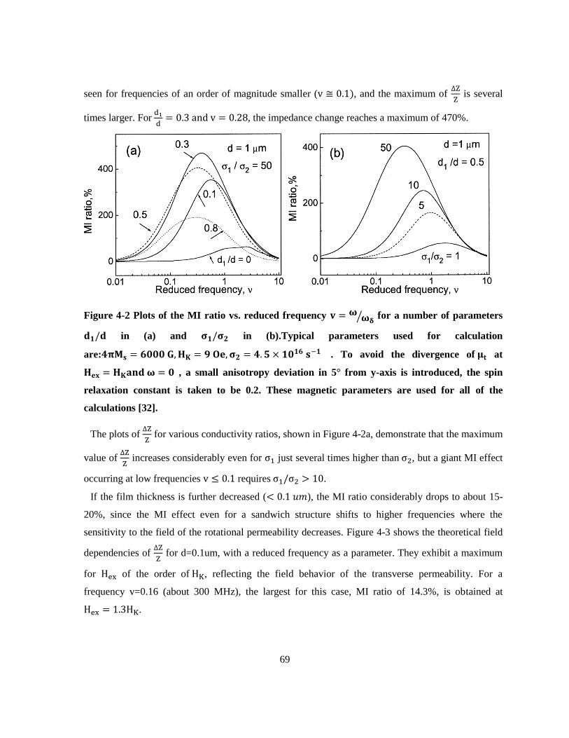
69
seen for frequencies of an order of magnitude smaller (v ≅ 0.1), and the maximum of ∆Z
Z is several
times larger. For d1
d= 0.3 and v = 0.28, the impedance change reaches a maximum of 470%.
Figure 4-2 Plots of the MI ratio vs. reduced frequency 𝐯 = 𝛚𝛚𝛅⁄ for a number of parameters
𝐝𝟏/𝐝 in (a) and 𝛔𝟏/𝛔𝟐 in (b).Typical parameters used for calculation
are:𝟒𝛑𝐌𝐬 = 𝟔𝟎𝟎𝟎 𝐆,𝐇𝐊 = 𝟗 𝐎𝐞, 𝛔𝟐 = 𝟒. 𝟓 × 𝟏𝟎𝟏𝟔 𝐬−𝟏 . To avoid the divergence of 𝛍𝐭 at
𝐇𝐞𝐱 = 𝐇𝐊𝐚𝐧𝐝 𝛚 = 𝟎 , a small anisotropy deviation in 5° from y-axis is introduced, the spin
relaxation constant is taken to be 0.2. These magnetic parameters are used for all of the
calculations [32].
The plots of ∆Z
Z for various conductivity ratios, shown in Figure 4-2a, demonstrate that the maximum
value of ∆Z
Z increases considerably even for σ1 just several times higher than σ2, but a giant MI effect
occurring at low frequencies v ≤ 0.1 requires σ1/σ2 > 10.
If the film thickness is further decreased (< 0.1 𝑢𝑚), the MI ratio considerably drops to about 15-
20%, since the MI effect even for a sandwich structure shifts to higher frequencies where the
sensitivity to the field of the rotational permeability decreases. Figure 4-3 shows the theoretical field
dependencies of ∆Z
Z for d=0.1um, with a reduced frequency as a parameter. They exhibit a maximum
for Hex of the order of HK, reflecting the field behavior of the transverse permeability. For a
frequency v=0.16 (about 300 MHz), the largest for this case, MI ratio of 14.3%, is obtained at
Hex = 1.3HK.
70
Figure 4-3 The MI ratio as a function of 𝐇𝐞𝐱 for two frequencies v=0.04 and v=0.16, d=0.1um,
𝛔𝟐 = 𝟏. 𝟕 × 𝟏𝟎𝟏𝟕𝐬−𝟏and 𝛔𝟏
𝛔𝟐= 𝟏𝟐(related to NiFe/Cu/NiFe) [32].
4.2.1.1 Dependency to width of the strip (b)
Figure 4-4 shows the plots of the MI ratio vs. frequency with the film width as a parameter, while its
thickness is fixed at d=0.5 um and d1
d= 0.5. The calculation corresponds to CoFeSiB/Cu/CoFeSiB
films[32]. For a sandwich 100um wide, the result is very close to that obtained from the exact
solution Equation (33) for an infinite film. With decreasing b, the MI ratio drops and its maximum
shifts to higher frequencies. At frequency v=1 (around 250MHz), ∆Z
Z of a 100um-wide film has a
maximum of 360%, whereas a 10um-wide film shows only 75%. For these dimensions and
frequencies, and Hex ≅ HK, the characteristic parameter λ is estimated to be about 3um. Hence,
b=10um is comparable to 2λ. In general, the AC demagnetizing effect in the multilayer structures
essentially reduces the MI ratio if the film width but does not satisfy the condition of b ≫ 2λ.[32]

71
Figure 4-4 Plots of the MI ratio vs. frequency with the film width as a parameter: d=0.5 um
and d_1=d_2. The calculation is related to CoFeSiB/Cu/CoFeSiB films [37].
Based on the theoretical model, a simulation has been done to design samples with pick impedance
change at 10 Gausses. According to the simulation, two types of samples were designed, as follows:
Meander type structures
1 mm × 0.5 mm dimensions
Metal trace width: 10, 20, 50, and 100 μm
CoSiB overlap over the metal trace: 10, 20, and 30 μm
Straight wire test structures
10 mm length
Metal trace width: 10, 20, 50, 100, and 200 μm
CoSiB overlap over the metal trace: 10, 20, 50, 100, 200, 400, and 1400 μm
Simulation results for 1 mm x 0.5 mm resistors:
0.6 um Ag thickness, 200 um line pitch, R = 0.1 ohm, delta(Z) = 90% f = 10MHz.
60 nm Ag thickness, 40 um line pitch, R = 200 ohm, delta(Z) = 1% at f = 10MHz.
It should be noted that changing Ag to Au will have the same results and will even improve the MI
ratio.

72
4.3 COMSOL FEM Simulation
In 2002, Dong [46] presented an analytical model for the permeability change in Giant magneto-
impedance metallic glass materials over a frequency and external magnetic field. This analytical
model is derived from the Launda-Liftshitz equation. In order to set up the COMSOL simulation, we
used the permeability equations to calculate the real and imaginary permeability factors. The results
are shown in Figure 4-5 and Figure 4-6.
Figure 4-5- The calculated dependence of μ’; the real part of effective permeability, on applied
external magnetostatic field Hext

73
Figure 4-6 The calculated dependence of μ”; the imaginary part of effective permeability, on
Hext
After calculating these two variables in MATLAB, the data of these two graphs was fed to COMSOL
to solve the GMI equations. In the COMSOL simulation, an AC/DC module is employed with the
magnetic and electrical field activated. In order to make it easier for simulation, the meander-shaped
devices were assumed to be linear and their total length projected in a linear multilayer GMI
structure. A frequency range of 200 kHz to 40 MHz is simulated in this work. In the simulation setup,
the AC current is passing the conductive layer (Au) from the upper and lower planes, while the other
boundaries are set to insulation. The simulation results are illustrated in the following figures. Figure
4-7 shows the circumferential magnetic flux of the sensor at 1 MHz. This magnetic flux is a result of
the current density inside the device.

74
Figure 4-7 Circumferential magnetic flux of the sensor at 1 MHz
In order to see the current density inside the device and study its distribution, the current density on a
cross session area is plotted in Figure 4-8. The figure reveals the skin effect in this structure. It is
obvious that the current tends to pass through the edges of the cross section area. Another interesting
point in this graph is the leakage of the current from the conductive material to the magnetic one. This
leakage and accumulation of portion of the current on the edges of the magnetic layer causes the
increase in the impedance in higher magnetic fields and frequencies. This leakage is the cause of MI
phenomena in multilayer structures.

75
Figure 4-8 Current density distribution along the cross section under the external field of 2400
A/m
Figures 4-9 to 4-14 show the calculated impedance for different frequencies.

76
Figure 4-9 Simulation results for impedance of the GMI sensor at 200 kHz

77
Figure 4-10 Simulation results for impedance of the GMI sensor at 500 kHz

78
Figure 4-11 Simulation results for impedance of the GMI sensor at 1 MHz
Figure 4-12 The impedance of sample for different ac frequencies under various external
magnetic fields.

79
4.3.1 Study the effect of thickness
Increasing the length has a significant effect on increasing the MI ratio. However, increasing or
decreasing the width does not have any effect, as long as the overlap remains constant.
Figure 4-13 Left) impedance of R-50-30 GMI sensor with 2 um thickness at 1 MHz, Right)
impedance of R-50-30 GMI sensor with 1 um thickness at 1 MHz,
Figure 4-14 Left) impedance of GMI sensor with 2 um thickness at 500 kHz, Right) impedance of GMI sensor with 1 um thickness at 500 kHz,

80
4.4 Fabrication Process
4.4.1.1 Material Research
The GMI layer used in this research is CoSiB, and the deposition of this material was done using a
sputtering process. As fabrication of this material is new to CIRFE and UWATERLOO, a
characterization process was done to develop the fabrication process. The characterization process is
reported below:
Deposition rate determined for 2 recipes
o DC Sputtering Recipe #1: 1.67 Å/s
o Pressure = 1.5 mTorr (15 SCCM Ar flow)
o Power = 300 W
o DC Sputtering Recipe #2: 3.1 Å/s
o Pressure = 1.5 mTorr (15 SCCM Ar flow)
o Power = 600 W
Adhesion properties
o No adhesion layer is required
o The samples survived the adhesive tape test on both glass and Si wafers
Etching process developed
o Less than 1 um undercut
o Features as small as 10 um can be fabricated
o Etchant: Ni Etchant Type I Transene + BHF dip
Etchant selectivity is very poor
o Etch rate in gold etchant: > 12 nm/s
o Etch rate in Cr (CR14) etchant: > 12 nm/s

81
Electrical resistivity determined: 18.7 µΩ.m
4.4.1.2 Fabrication Process
The fabrication sequence is illustrated in Figure 4-15:
Figure 4-15 Fabrication process sequence of GMI samples.
GMI thin film magnetic sensors were fabricated on 3-inch glass wafers. At the outset of the
fabrication process, the wafers were placed for RCA cleaning, after which the deposition of CoSiB
using the intelvac deposition system was done. The deposition is performed as a DC sputtering in
1.5mTorr (15 SCCM Ar flow) pressure and with 600W of power. The measured deposition rate was
3.1 Å/s. In the next step, the deposited CoSiB layer was patterned using positive photoresist;
unwanted parts were etched away using a Ni etchant. The accuracy of the patterning step yielded a
10-um feature size. Following the characterization of the wafers in this step, 2um of undercut was
observed, as shown in Figure 4-16.

82
Figure 4-16 Undercut of CoSiB sample.
A thin film adhesive layer like Ti needs to be deposited on top of the wafers. This layer is also
needed to save the CoSiB layer from etching by an Au etchant; otherwise, the wet-etching of the layer
will be unsuccessful, as the CoSiB layer is attacked by Au etchants at rates faster than Au. A thicker
Ti barrier/stiction layer is required that will undermine the potential performance of the device.
Therefore, in this step, a Ti/Au/Ti metal layer is deposited and patterned. Afterwards, Gold
resistivity, measured by the Van der Pauw method and with a sheet resistance equal to 92 mΩ.
Ti/Au/Ti, is patterned, using the lift-off process. It should be noted that the kwik strip solution mildly
but negligibly attacked the CoSiB layer.
Optical images of fabricated GMI samples are shown in Figures 4-17 and 4-18. In Figure 4-17, the
two different types of samples are illustrated. These devices have the following design rules:
o Meander type structures
1 mm × 0.5 mm dimensions
Metal trace width: 10, 20, 50, and 100 μm
CoSiB overlap over the metal trace: 10, 20, and 30 μm
o Straight wire test structures
10 mm lenght
Metal trace width: 10, 20, 50, 100, and 200 μm

83
CoSiB overlap over the metal trace: 10, 20, 50, 100, 200, 400, and 1400 μm
Figure 4-17 A view of one batch of fabricated sensors. Two categories of devices are shown in
this figure.
Figure 4-18 Various types of minder shape GMI sensors.

84
4.4.2 Test Setup and Measurement
The devices are tested using a custom-made experimental setup. An external magnetic field is
exerted, employing a Helmholtz coil. The custom-made setup is fabricated with aluminum which,
because it is not a magnetic material, will not affect the magnetic flux streams of coil. The other
instruments employed as setup components are 4 DC probes with micro-positioners and an optical
microscope. Figure 4-19 shows the setup components.
Figure 4-19 DC probes and measuring the variation of impedance under magnetic field in GMI
samples.
The impedance is measured with two different methods and systems and the results are compared at
the end. The first method is a 4 point probe measurement using oscilloscope and second one is using
an advance precision impedance analyzer from Agilent.

85
4.4.2.1 Impedance measurement with Oscilloscope
The impedance measurement setup includes a function generator, an oscilloscope, and one known
resistor in the order of DUTs (device under test) resistance. Figures 4-20 and 4-21 illustrate a
schematic of the measurement setup and a picture of the measurement setup, respectively.
Figure 4-20 Schematic of measurement setup.
Figure 4-21 The measurement setup.

86
To measure the impedance of the system, a known resistor is connected in series with the DUT, and
the voltage drop over the sample and the resistor is measured. (Note that the DUT and resistor
currents can be calculated from the voltage drop over the resistor.) The DUT impedance is
subsequently calculated from the device’s voltage and current. Using this setup, 𝑉𝐷𝑈𝑇 and 𝑉𝑅 are
captured and then processed in MATLAB to calculate the impedance and phase of the signal. The
impedance of DUT is calculated using Equation (37):
𝑍𝐷𝑈𝑇 = 𝑅𝑉𝐷𝑈𝑇
(𝑉1 − 𝑉𝐷𝑈𝑇)
(37)
4.4.2.1.1 Experimental results
Some of the samples were tested under the magnetic field and various frequencies. The results are
shown in Figures 4-12 to 4-14.
Figure 4-22 Impedance magnitude and phase of Device R10-40-1.

87
Figure 4-23 Impedance magnitude of Device R10-40-1 at1 and 10 MHz.
Figure 4-24 Impedance magnitude of Device 50-30 at1 and 10 MHz.

88
4.4.2.1.2 Discussion and Conclusion
o The measured impedance and phase of the devices increases with signal frequency
due to enhanced inductance of the line.
o At f = 1 kHz, the impedance of the devices does not increase with applied magnetic
field.
o When the impedance and phase are calibrated (using short and open measurements),
the same trend is observed in impedance magnitude but not in the phase.
o The measured / calibrated impedance of the device at 10MHz is not valid, as after the
calibration, negative impedance is achieved for the phase. This is due to the parasitic
inductors of the measurement setup having higher impedances values compared to
the device.
I- Slight increase of the impedance magnitude is observed at the 5-10 G external magnetic field
o The impedance change is less than 1% for R10-40-1 design at 1 MHz.
o The impedance change is less than 5% for R5030 design at 1 MHz.
o The impedance measurement may not be valid at 10 MHz due to measurement setup
parasitics.
II. To find an alternative way to magnetize GMI material, we started some preliminary tests. Our
preliminary test with ferromagnetic materials showed that we can make them like a
permanent magnet by annealing them under magnetic field. Thus, we studied the effect of
thermal and magento thermal treatment on our fabricated samples, the results of which are
reported in Chapter 5. As a result of the characterization study, we ended up performing a
magneto-thermal treatment on our samples. The treatment parameters time, temperature and
magnetic field all have a corresponding effect on the device performance. During high
temperature annealing, the magnetic domains in ferromagnetic material were expected to lose
their walls and fall in line with the external exerted magnetic field. A schematic of the
magnetization the occurred in the annealing step is shown in Fig 4-25. One of the main
challenges here would be protecting the thin films from becoming oxidized in the hot
temperatures. This challenge has been overcome by performing the annealing in nitrogen
ambient. An Energy-dispersive X-ray spectroscopy (EDX) confirms the negligible oxidation
after the process. Applying this process will reduce the cost and workload of the fabrication
process.

89
Figure 4-25 Schematic of magnetization process in magneto-thermal annealing step
The fabricated set of sensors was first annealed in a nitrogen environment furnace at 300 °C for
three hours, with two 1000-G high temperature permanent magnets located under the samples. By
performing the same measurement in these samples, and as reported in Figures 4-24 and 4-26, there is
a marked improvement in the change of impedance. The preliminary measured results after annealing
are illustrated in Figure 4-26. Here, it can be seen that the GMI R-50-30 samples at 200 kHz and 500
KHz measurement frequencies exhibit increased impedance magnitudes of 36% and 45%,
respectively; in contrast, R-40-10 shows increases of only 17% and 21% at these frequencies. These
data show promising improvements from the measured data before the post-processing step.

90
Figure 4-26 Measured impedance of two different GMI devices with different dimensions. As
expected, the sensor demonstrates a substantial increase in impedance at higher excitation
frequencies.
We propose developing the annealing process and optimizing its parameters for GMI magnetic
sensors. The detailed study on this optimization and characterization can be found in the next chapter.
The intended function of these sensors is to enable or disable a logic circuit.
The fabricated device will be mounted on a Wheatstone bridge. Exposure to a magnetic field of 10
G will cause the sensor impedance to change and the Wheatstone bridge to assume an unbalanced
position. As a result of this instability, an On/Off circuit will be activated. The Wheatstone bridge and
the DUT in its system are shown in Fig. 4-27. To achieve better sensing accuracy, the circuit can be

91
designed as unstable by default. Thus, by inserting a magnetic field when the sensor is sensing the
desired amount of field, its impedance will increase and the bridge will achieve a stable condition,
which will cause the current G to become zero. The reported results show a satisfying range of
impedance change for the Wheatstone bridge’s proper performance.
Figure 4-27 Wheatstone bridge and DUT in final sensor.
The integration will help create a 0/1 digital sensor for a narrow band of the magnetic field. The result
will yield two types of sensors: one with high sensitivity, and one with low sensitivity. In a high
sensitivity sensor, the bridge is normally unstable and the circuit is off; when the GMI sample reaches
the desired impedance (which is a function of the magnetic field), the bridge will go to stable mode
and the circuit will be on. When the device is turned on, a logic circuit will run and let us know that
our exact desired field is sensed. In low sensitivity mode, the bridge will be normally stable and
therefore the circuit normally on. After sensing a known amount of magnetic field and above, the
impedance will change and break the stable mode. At this point, the circuit will go off and we will be
notified of the existence of a measurable range of magnetic field around the sensor.
In order to ensure the quality of the measurement in this section, an Agilent precision impedance
analyzer E4990A is employed. A detailed study of measurements using this device is reported in the
next section.

92
4.4.2.2 Impedance Measurement Using Agilent Precision Impedance Analyzer
E4990A
Agilent E4990A is a precision impedance analyzer with the ability to do measurements in a sweep
frequency range of 20Hz to 120 MHz. This device empowered us to do the measurements in different
frequencies and compare the results with the old measurements. Below, a summary of measurement
results is presented.
In order to see the effect of frequency at a constant magnetic field, one can slice the graph at the
desired magnetic field. To see the impedance changes at a constant frequency, the same slicing can be
done on a 3D graph at the desired frequency. Figure 4-29 shows the changes in impedance at a
constant magnetic field. As shown in the figure, frequency increases result in impedance increases. It
is also notable that the frequency effect on impedance has almost the same trend for different
magnetic fields. From this graph, if we cross a vertical line at 500 kHz, the data from Table 4-1 can
be captured.
Figure 4-28 Impedance of GMI sample, R-50-30, measured in different magnetic fields in a frequency sweep of
150 Hz to 10 MHz

93
Figure 4-29 Measured impedance for R-50-30 (this is the same sample as previous section) at
constant external magnetic fields over a frequency sweep
Table 4-1 Impedance Values for GMI R-50-30 at 500 kHz Measured with Agilent Impedance
Analyzer
Frequency 0 G 5 G 8 G 10G 15 G 20 G
5.00E+05 16.95
ohm
17.76
ohm
22.46
ohm
27.07
ohm
24.91
ohm
19.30
ohm
It should be noted that in order to compare the measured value with the previously measured data
from the other method, the same sample is tested here. Table 4-2 shows the measured value of this
sample with Oscilloscope measurement. Using the data in these two tables, Figure 4-30 illustrates the
impedance graph of this sample measured in each method.
0.00
20.00
40.00
60.00
80.00
100.00
120.00
140.00
160.00
-1.00E+06 1.00E+06 3.00E+06 5.00E+06 7.00E+06 9.00E+06 1.10E+07
0 G
5 G
8 G
10G
15 G
20 G

94
Table 4-2Measured Values for GMI R-50-30 in Oscilloscope Measurement of Impedance
R-50-30 500khz
B R(ohm) V1(V) V2(V) V1-V2(V) R short (ohm)t Z (ohm)
0 20 3.6 1.98 1.62 7.75 16.69444
5 20 3.6 2.02 1.58 6.36 19.20962
10 20 3.32 2.06 1.26 6.36 26.33841
15 20 3.32 1.98 1.34 6.5 23.05224
20 20 3.6 1.98 1.62 6.44 18.00444
short condition: 2.32 0.56 1.76 6.363636
To make a better comparison, both of these graphs are depicted in the same graph in Figure 4-25,
along with simulation data for the same sample in the same frequency. As shown in the figure, the
simulation results are in a good agreement with the measured values of the two methods.
15
17
19
21
23
25
27
0 10 20 30
Imp
ed
ance
(o
hm
)
R-50-30 GMI sensor measured with Oscilloscope
500 kHz
15.00
17.00
19.00
21.00
23.00
25.00
27.00
0 G 5 G 8 G 10G 15 G 20 G
R-50-30 GMI sensor measured with Agilent
500 kHz
Figure 4-30 The measured impedance for GMI R-50-30 which suing both measurement methods.

95
Figure 4-31 A comparison of 3D simulation for GMI R-50-30 and the measured impedances
captured with Impedance analyzer (Blue) and Oscilloscope (Red)
After characterizing the post-processing (the details of which are reported in next chapter), sample R-
50-30 was processed in the optimal treatment condition. This optimal processing is a magneto-
thermal treatment of sample at 550 C for 3 hours in nitrogen ambient. Two ultra-high temperature
permanent magnets with magnetic field of 1000 G were place under the die of sample. Figures 4-26
and 4-32 show the new measured values for the impedance of this sample.
15.00
17.00
19.00
21.00
23.00
25.00
27.00
0 G 5 G 8 G 10G 15 G 20 G
Comparison of various measurements and 3D simulations
LCR Meter
Oscilloscope
COMSOL Simulation

96
Figure 4-32 Measured impedance for R-50-30 (this sample is post process at the optimal
processing condition) at constant external magnetic fields over a frequency sweep
Figure 4-33 Impedance of R-50-30 sample annealed in optimized condition
0.00
20.00
40.00
60.00
80.00
100.00
120.00
140.00
160.00
0.00E+00 2.00E+06 4.00E+06 6.00E+06 8.00E+06 1.00E+07 1.20E+07
0 G
5 G
8 G
10G
15 G
20 G
15.00
20.00
25.00
30.00
35.00
40.00
0 G 5 G 8 G 10G 15 G 20 G
New R-50-30 500 kHz
500 kHz

97
Figure 4-33 shows an MI ratio of 141%. This is a tremendous improvement in impedance value of the
sample with respect to the unprocessed sample and the previously processed samples. Figure 4-34
shows a comparison of measured impedance and MI ratio for R-50-30 in respect to simulations
results for higher frequencies.
Figure 4-34 Comparison of experimental measurement and simulation results for frequency
range of 1 MHz to 10 MHz.
Figure 4-35 shows the dependency of MI ratio and impedance to frequencies in higher frequencies.

98
Figure 4-35 Maximum GMI as a Function of frequncy

99
5 Chapter Five
Characterization of GMI material- CoSiB
In this chapter, CoSiB alloy is developed to enhance the performance of multilayer thin film GMI
sensors. The material is investigated for several different post-processing thermal and magneto-
thermal treatments, which are categorized to study the effect of temperature, time, and the existence
of an external magnetic field. The prepared samples are tested with various magnetics and material
characterization tools in order to obtain a detailed understanding of the process and its effects. The
post-processing shows a significant impact on the magnetic properties of the material. The causes of
this impact are studied in detail. It is shown that CoSiB with enriched magnetic properties has some
nano-clusters of cobalt in its amorphous matrix structure. The post-process technique can be
employed to facilitate cost-effective fabrication of GMI structures in conventional micro-fabrication
facilities.
5.1 Introduction
Sensor technology is one of the most attractive topics to scientists today, both in academia and in
the industry [1]. Magnetic sensors are widely employed in various technological fields such as
geology, aeronautics, maritime navigation, and the automobile and medical sectors [1-6]. The keen
interest in developing reliable, accurate, and miniature sensors makes giant magnet-impedance (GMI)
sensors an ideal solution. A giant magneto-impedance phenomenon is the change in impedance of a
high-permeability material with a DC magnetic field. This occurs due to the skin effect and skin depth
changes in different frequencies [5-10].
The GMI effect has been extensively studied in ferromagnetic wires and ribbons because of the
main applications of sensing [6-8]. Recently, some multilayer GMI sensors that take advantage of
thin film technology were introduced [3, 9-13]. Because of the dimensions of the thin films, the recent
multilayered sensors have enhanced sensitivity to the skin effect and could show better results even at
lower frequencies [9-12].

100
In a multilayer GMI structure, a conductive layer is sandwiched with layers of GMI material and
will exhibit changes in the impedance upon sensing an external magnetic field. The GMI material in
these structures is magnetized toward the easy axis of the device. The fabrication process of the layers
and devices is a unique and highly expensive process that prevents the use of normal microfabrication
machines [5, 6, and 8]. This makes them unattractive from an industry perspective.
On the other hand, beyond the study of giant magneto-resistive sensors from a materials point of view
[14, 15], many studies have been carried out on the characteristics of GMI material, with the end goal
of discovering an alternate (i.e., less ‘exotic’ and thus more cost-effective) fabrication method for
these structures. In our previous work [44 and 45], we fabricated and reported on a multilayer GMI
sensor with conventional microfabrication, and did a post-process procedure on devices to expose the
GMI phenomenon. In this study, an extensive post-processing study has been implemented on the
GMI material CoSiB, and the characterization results are reported and discussed.
5.2 Fabrication and Post-Processing
In this study, a CoSiB amorphous metallic alloy is deposited and investigated. The alloy employed
in this study is Co73S12B15, but we later find that the same behavior is expected for the same family
of material. The alloy has been sputtered in a DC magnetron sputtering system. Sputtering was
performed in Ar plasma at a pressure of 1.5 mTorr and 600 W of DC power at a rate of 3.1 Å/s.
Three-hundred nm of material was deposited on a glass wafer, after which the wafer was diced to 1
by 1 cm dies.
In order to perform a meaningful study on post-processing effects, we examined the effects of
thermal treatment versus those of magneto-thermal treatment. We also studied the effects of
annealing dwell time and temperature on the structure: The post-processing was carried out in two

101
main categories: a) thermal treatment, and b) magneto-thermal treatment. In each category, the
samples are processed over two different dwell times: 3 and 4 h. Furthermore, in each category, the
thermal treatments include annealed samples in 300 to 700 °C, with 100 °C increments. The
annealing process was done in a clean room using a high-temperature oven with nitrogen ambient.
The detailed processes of the samples are as follows:
a) thermal treatment:
In the thermal treatment, the samples are annealed in the oven with nitrogen ambient in dwell
temperatures of 300, 400, 500, 600, and 700 °C. The rise time of all annealings was 1 h, and the dwell
times were 3 and 4 h. The samples were then cooled to room temperature.
b) magneto-thermal treatment:
In the magneto-thermal treatment two 1000 G high-temperature permanent magnets were placed
under the dice of the samples in the oven provided with the external DC magnetic field during the
annealing process. With this DC magnetic field, the same thermal process as discussed in a) was
implemented on a batch of samples.
5.3 Magnetic Characterizations
After the post-processing, all the samples were characterized to identify their magnetic properties.
Permeability and AC susceptibility (in-phase component X' (m³/kg)) was measured with a model
KLY-2 Kappabridge, and hysteresis loops were measured with a Princeton Measurements model
3900 MicroMag vibrating sample magnetometer (VSM) using a maximum field of 1 T.

102
5.3.1 Permeability Measurement
The relative permeability was measured for both categories of samples, and the results are illustrated
in Figures 5-1 and 5-2.
Figure 5-1 The relative permeability of samples thermally treated for 3 h; (b) the same for
samples annealed for 4 h.
Figure 5-2 (a) The relative permeability of samples treated magneto-thermally for 3 h; (b) the same for
samples annealed for 4 h.

103
Figures 5-1 and 5-2 confirm enhancement of the relative permeability under the thermal treatment.
Based on the measurements, the existence of an external magnetic field does not have a significant
effect on the permeability improvement of the alloy. It is worth noting that except for the high peaks,
the measured points for the magneto-thermal samples have a higher general average of relative
permeability than the thermal ones.
Moreover, the results also show a high peak of relative permeability forming around 600 °C. The high
peaks of permeability for all four conditions are reported in Table 1:
Table 5-1 High Peaks of The Relative Permeability for Different Post-Processing Conditions
Type of Post-
process
Dwell Time
(h)
Dwell
Temperature
(°C)
Peak of
Relative
Permeability
(μr)
Thermal 3 600 3615.56
Thermal 4 500 2868.37
Magneto-thermal 3 600 3551.82
Magneto-thermal 4 600 2446.96
Based on the achieved results, we can see that samples could reach a higher permeability of
approximately 3500 μr in 3 h of treatment for both thermal and magneto-thermal processes. We think
the local minimum captured in the relative permeability graph of 4 h of magneto-thermal processing
could be an error. If the local minimum in Figure 5-2 is assumed to be a measurement error, it can be
concluded that the longer annealing dwell time of 4 h leads to a broader relative permeability peak,
which allows the user to achieve higher permeability in lower annealing temperatures. As shown in
Figure 1, for samples treated for 3-h the recorded permeability of thermal process was 2025 μr at 400
104
°C, whereas it was 2425 μr for the same temperature and 4 h of annealing. Similarly, Figure 2 also
shows 1876 μr for samples treated for 3 h at 300 °C, whereas the relative permeability was 2411 μr
for the same temperature but 4 h of treatment. This can prove beneficial for devices with high-
temperature limitations in their structures.
The reason for permeability enhancement in the alloy is the formation of nano-clusters of Co within
the entire amorphous metal structure. These nano-clusters, which are discussed later in this work,
have the main impact on permeability change without changing the morphology of the whole alloy.
5.3.2 Hysteresis Loop and Magnetization
Samples are measured for magnetic hysteresis loop, and the results show mass normalized values.
The samples are given a nominal mass of 1 g and a nominal volume of 1 cm3 in order to ease the
calculations. Hysteresis is present in ferromagnetic materials and materials with magnetization ability.
As soon as a magnetic field is applied, the material becomes magnetic until all the Weiss domains of
the material have the same orientation and directions. This state is the maximum magnetization of
material. When the external magnetic field is removed, some materials retain a considerable amount
of magnetization and remain magnetic. This is the main feature in forming a hysteresis shape [4], and
thus a larger loop area represents better magnetization. The hysteresis loop and magnetization curve
of the studied post-processed CoSiB are presented below:

105
Figure 5-3 (a) The hysteresis loop of samples thermally treated for 3 h; (b) the same samples
annealed for 4 h. The square marker shows the loop for the process with the highest
permeability, and the triangle marker is for the after fabrication (AF) sample.
Figure 5-4 (a) The hysteresis loop of samples magneto-thermally treated for 3 h; b) the same
annealed for 4 h. The square marker shows the loop for the process with the highest
permeability, and the triangle marker is for the after fabrication (AF) sample.

106
Based on Figures 5- 3 and 5-4, the post-processing improves the magnetizability of the GMI material.
The higher magnetizability leads to better magnetization of the GMI layer in a multilayer sensor,
which is done by a magneto-thermal process.
5.3.3 Magnetization of CoSiB Layer in a layered structure
After the magnetic properties of the GMI material are improved, the material should be magnetized
in order to show the GMI phenomenon and be employed in a multilayer GMI structure. As
demonstrated in section III-b, the material has a high potential of magnetization in some known post-
processes conditions. A magneto-thermal treatment in specified temperature and time will result in
breaking the Weiss domains’ walls. Upon losing the magnetic walls, the magnetic domains of
material will align in the direction of the exerted magnetic field. This process bypasses the need for a
special and expensive sputtering system for GMI material fabrication. Figure 5-5 shows a schematic
of this process.

107
Figure 5-5 Schematic of annealing magnetization under a magneto-thermal post-process. It is
shown how the Weiss walls are breaking up and letting the domains be aligned to the external
field.
5.4 Material Characterizations
For material characterization, the material is tested using Raman spectroscopy, X-ray diffraction,
and energy dispersive X-ray spectroscopy. In the following sections, measurements for each test are
illustrated.
5.4.1 Raman Spectroscopy
A Raman test is done on the CoSiB before and after the annealing step to see whether or not the
crystallization of material changes during this step. The narrowing and increasing in the intensity of

108
the Raman band, as well as the shifting in the bands to higher wave numbers, can be attributed to an
increase in particle size and improved crystallinity. The Raman test is implemented using Raman
spectroscopy and a microscopy machine, Bruker Senterra Confocal Microscope (with 532 and 785
nm lasers). The result of Raman spectroscopy supports the preliminary expectations for higher
crystallinity after the treatment. It also shows high quality small-sized crystals of Co in the spectrum.
Figures 5-6 and 5-7 give the Raman spectroscopy results for thermal and magneto-thermal samples.
Figure 5-6 Raman spectroscopy for thermal post-processed samples.
Figure 5-7 Raman spectroscopy for magneto-thermal post-processed samples.

109
In Figures 5-6 and 5-7, the condition which had the highest permeability is bolded in the graphs. It
is interesting to note that the condition corresponding to the highest permeability has higher intensity
and better quality peaks in the Raman spectroscopy results as well, which confirms the formation of
nano-crystals in the entire metallic glass structure of CoSiB. Another interesting fact in the Raman
test is that the treatment of samples at higher temperatures makes a better quality of nano-crystallines
until the highest permeability point, after which the crystals lose their quality and vanish. This is due
to the probable formation of equilibrium phases of material at temperatures higher than 650 °C.
Among those phases, it is probable that boride phases such as Co3B and Co2B will be formed. Boride
phases normally decrease the relative permeability of materials [4, 16]. Figures 5-1 and 5-2 verify the
assumption of boride formation in temperatures above 650 °C, as they confirm the decreasing of
permeability at this temperature.
5.4.2 X-Ray Diffraction
X-ray diffraction (XRD) is done on samples using a bruker d8 advance X-Ray diffractometer
system with the capability of testing thin films. The XRD parameters for the experiment are reported
in Table 5-2.
Table 5-2 X-Ray Diffractometer Parameters
Parameter Value
Current intensity of X-ray tube 40 mA
Voltage of X-ray tube 40 kV
Beam wavelength 0.154 nm
Time of counting in one measurement point 5 s
Step between measurement points 0.05 °
Range of scan 20-80 °

110
Figures 5-8 and 5-9 illustrate the XRD measurement for thermally treated and magneto-thermally
treated samples, respectively.
Figure 5-8 XRD graphs of samples thermally treated for 3 and 4 h.
Figure 5-9 XRD graph of samples magneto-thermally treated for 3 and 4 h.

111
In Figures 5-8 and 5-9, some peaks can be detected in specified angles. Checking these peaks with
X'Pert Highscore Plus software (provided with the XRD diffractometer) and comparing the peaks
with those found in other research reports reveals that they are all showing -Co crystalline. The fact
that only Co crystalline is detected in XRD supports the idea of the formation of Co nano-clusters in
the matrix of an amorphous metallic alloy. Normally in an XRD graph, a higher intensity of baseline
is related to a higher quality of amorphous structure. As is shown in Figure 5-8 and 5-9, the baselines
of captured streams have high intensity values; even the stream with the crystalline shows a general
amorphous structure. For the above data, and using the Scherrer method [17] in the software, the
crystallite size of the Co nano-clusters is calculated at around 2.5 nm. In this method, the size is
calculated using the Scherrer equation, which relates the size of a crystallite to the beam wavelength,
peak angle, and full width at half maximum (FWHM) of the peak [17].
5.4.3 Energy Dispersive X-Ray Spectroscopy
In order to determine the elemental composition of specimens and ensure that the samples have the
same alloy ratio as the sputtering target, energy dispersive X-ray spectroscopy (EDX) is performed on
samples. The measurement is done using a TEAM EDS analysis system for SEM. EDX
measurements for all of the samples are the same, and the same results are captured. The results
indicate that annealing does not change the alloy structure and that no external chemical reaction
occurs in the main material. Figure 5-10 shows the EDX of a sample thermally treated for 3 h at 600
°C.

112
Figure 5-10 EDX graph of a sample magneto-thermally treated for 3 h at 600 °C. It should be
noted the same graph is captured for all other samples.
Table 5-3 shows the quantitative measured values for this experiment.
Table 5-3 EDX Captured Quantitative Results. The Main Elements are Highlighted
Element Weight% Atomic%
B K 11.31 20.99
C K 1.69 2.01
O K 2.44 3.14
Co L 72.85 57.52
Si K 10.28 12.98
Al K 0.6 0.72
Ca K 0.83 2.64
As can be observed from Table 5-3, the main captured elements are Co, Si and B, with almost the
same weight distribution in the alloy as the source of the sputtering. Some other elements with

113
negligible amounts are also detectable, but these correspond to sample contamination and test
environment.
5.5 Results and Discussion
Based on the achieved results for the various magnetic and material characterization tests, it can be
concluded that CoSiB GMI material keeps its elemental composition and amorphous shape in post-
processing treatments. Furthermore, the results show that some nano-crystallines of Co formed in the
amorphous matrix of material. These nano-crystals are congregated together as nano-clusters of Co in
the matrix. The formation of Co nano-clusters is the main reason for permeability enhancement in the
material. Experiments also indicate the critical temperature at which the highest permeability can be
reached. A detailed study of the material properties of the CoSiB confirms the formation of small
nano-crystallines of -Co in the structure.
Moreover, the tests show that the high level of background baseline in XRD measurements
confirms the morphology of the material as metallic glass. According to the Raman spectroscopy of
the material, the quality of nano-crystals decreases after a critical temperature is reached. This occurs
due to the formation of equilibrium phases of material in the alloy, e.g., boride phases. The probable
boride phases have a reverse influence on magnetic enhancement, which results in a decrease in
permeability. This reduction in permeability can be verified in Figures 5-1 and 5-2 for samples treated
at 700 °C.
When viewing this research work, a misconception may arise regarding the source of enhancing
magnetic properties of CoSiB. Specifically, it might be assumed that thermal treatment is the sole
significant process in enhancing CoSiB’s magnetic properties and that a magneto-thermal process
will have exactly the same effect, but this would be an inaccurate assumption. To resolve this
misconception, note that in order to be able to use CoSiB as a GMI material, especially for a

114
multilayer structure, the material not only should have high permeability but also must be
magnetized. A magneto-thermal post-process leads to both of these properties. At a high temperature,
after removing the magnetic domain walls, the domains are all magnetized in the direction of the
external magnetic field and cool down in the same magnetic environment, ensuring layer
magnetization by the end of process.
In previous publications [3, 10], the authors reported fabrication and testing of multilayer GMI
sensors with a magneto-thermal post-process. The reported sensors indicate an impedance increase of
16.69 to 26.33 Ω, and 102 to 123.75 Ω for two different sensors. Since different elemental ratios of
CoSiB can be employed as GMI material with the same material morphology and behavior, the above
conclusions and qualitative patterns are valid for all CoSiB amorphous metallic alloys.
.
5.6 Experimental Tests on Tri-Layer Thin Film GMI Sensors
A batch of tri-layer thin film GMI sensors is fabricated using the same fabrication recipe. The
sensors consist of CoSiB(400nm)/Au(200 nm)/CoSiB(400 nm). The schematic of the fabrication
steps and an optical image of the batch of sensors are illustrated in Figure 5-11. Details of the
fabrication of these sensors can be found in the authors’ previous works [9 and 10].

115
Figure 5-11 GMI thin film samples fabrication process flow a) sputtering and patterning of
CoSiB b) Deposition and patterning of Metal trace layer c) sputtering and patterning of CoSiB
d) A 1-inch to 1-inch die of glass wafer, containing the thin film GMI samples.
The devices are tested using a custom-made experimental setup and employing Agilent E4990
precision impedance analyzer. Using a Helmholz coil [19], an external magnetic field is exerted on
the samples. The sample stage is made of aluminum that is not a magnetic material and will not affect
the magnetic flux streams of coil. The test results of one of the samples R-50-30 is reported below. In
this sample, the width of CoSiB layer is 50 μm and the width of the Au layer is 30 μm. Three R-50-30
are tested in 3 different phases: immediately after fabrication; after 300 C magneto-thermal after 600
C magneto-thermal treatment and 500 kHz of AC current. The results are shown in Figure 5-12.

116
Figure 5-12 Measurement results of GMI R-50-30 in 500 kHz ac current.
As illustrated above, the magneto thermal treatment has drastically increased the impedance change
in the tested thin film GMI sensor.

117
6 Chapter Six
Conclusions and Future Plans
The main focus of this work was realising miniature magnetic sensors. Miniaturizing sensors makes
it easier to integrate them with conventional industrial systems and also makes them useful for
biomedical applications. Due to high industrial demand for digital 0/1 magnetic sensors in the
millitesla range (also known as low field intensities), the goal spec of the sensors was set to this
working range. This magnetic field is not harmful to the human body and is in the range of fields
generated by biomedical devices. A main application of these devices is hearing aids. Typically when
using hearing aid devices, the user cannot speak on a phone or cellphone because a beeping noise
occurs in their ears. This problem arises from the conflict between the magnetic field in the hearing
aid and that in the speaker. In these cases, cutting one of the fields will resolve the problem. By
integrating a miniature magnetic sensor, the hearing aid’s magnetic field will be cut when it senses a
threshold field of noise generation.
After conducting a broad literature review on the recent advancements of magnetic sensors, we
chose two different types of sensors which we deemed well-suited to the scope of the research:
1- MEMS reed sensors
2- Giant Magneto Impendence (GMI) sensors
As reported in the thesis, both of these sensor types were studied in detail, and a miniature version of
them was successfully fabricated and tested. Contributions
1- Development of tri-layer MEMS Reed sensors:
A tri-layer MEMS reed sensor was designed, fabricated and tested in this thesis. The multilayer
beams were comprised of a Ni layer (3 μm bottom electrode, and 1 μm bottom electrode) sandwiched
between two gold layers (75 nm each). These sensors were studied and designed in COMSOL
Multiphysics, and were simulated in detail. Using the simulation results, the general working map of
these sensors was investigated and presented. The achieved sensors of this study were fabricated
using microfabrication technology. The full sensor size was around 300 μm * 100 μm, which is the
smallest fabricated MEMS reed sensor so far. The previously reported smallest MEMS reed sensor
was 1 mm * 1 mm, which is larger than our sensor by a factor of 10. The final fabricated sensors are
normally open switches that provide a 30 ohm contact upon actuation.
.

118
2- Development of multilayer Giant Magento-impedance thin film sensors:
In addition, this study presented the design and microfabrication of multilayer GMI thin film sensors.
The GMI multilayer is comprised of an Au layer (200 nm) sandwiched between two magnetic layers
(400 nm). GMI materials need an expensive sputtering system, which provides a magnetic field
during their deposition. A new post-processing treatment was investigated and tested that enabled the
fabrication of these materials using conventional microfabrication facilities. Moreover, a complete 3D
COMSOL simulation of GMI phenomena for multilayer thin film structures was presented. This
simulation was among the frontier efforts for simulating sensors using FEM simulation software.
Devices were designed based on the simulation results, and these were tested with two different
measurement methods. All of the captured results from the simulations and measurements were in the
acceptable range and verified each other. The GMI thin film sensors fabricated in this thesis showed
an MI ration of up to 100%.
3- Characterization of CoSiB material for GMI applications
CoSiB was studied and developed to be employed as a GMI material and enhance the performance
of multilayer GMI structures. This study is a complimentary investigation of post-processing
treatment and concludes the optimal post-processing treatment to achieve the best performance of the
GMI sensors. The characterization consists of various material characterization tests as well as
magnetic characterization tests. The tested samples were each treated at various dwell times and
temperatures. The characterizations show the formation of Co nano-clusters in the matrix of GMI
amorphous material as a result of the post-treatment. The formed Co nano-clusters were responsible
for the magnetic performance enhancement of these materials. To the best knowledge of the authors,
this thesis represents the first general study of the characterization of CoSiB as a GMI material.
6.1 Future Works
This thesis has carried out extensive research and investigations into a wide range of topics, aiming
to advance the development of miniature magnetic sensors and giant magneto-impedance phenomena.
There are several related research problems in this area that could potentially be explored in the
future. Below is a small sample of them:
Developing an array of MEMS sensors in order to sense multilevel threshold magnetic fields.
This can be helpful in applications sensitive to various levels of magnetic fields.

119
Integrate an on-chip magnetic coil in order to make the systems testable on-chip and
compensate the external magnetic field in necessary cases.
A more extensive study on the effect of time on the post-processing of GMI materials would
be beneficial. This study of time should be related to both the dwell time of treatments and
the cooling time of samples.
Ultimately, a GMI material could be employed as the core magnetic material of MEMS reed
sensors, and their performance enhanced with thermal treatment (as addressed in Chapter 5).
This integration could result in highly sensitive MEMS reed sensors that can be employed for
sensing lower magnetic fields. This could also be an initiative to futher miniaturize the
structures from the size achieved in this thesis.

120
Appendix A
Theory and mathematical equations for MEMS REED Sensors
Hybrid BIE/Poisson approach for magnetostatic analysis
The magnetostatic governing equations are derived from Maxwell’s equations and can be written as
[8]:
∇ × 𝑯 = 𝑱 (1)
∇.𝑩 = 0 (2)
where H is the magnetic field intensity, B is the magnetic flux density, and J is the current density. B
and H are related by the constitutive relation:
𝑩 = µ𝑯 = µ0µ𝑟𝑯 = µ0(𝑴 + 𝑯) (3)
where µ = µ0µr is the permeability of the magnetic material, µ0 is the permeability of the vacuum
and µr is the relative permeability of the magnetic material. M is the magnetization [8] of the
magnetic material and can be written as:
𝑴 = (µ𝑟 − 𝟏)𝑯 = 𝜒𝑯 =𝜒
µ(𝑩)
(4)
where χ is the magnetic susceptibility. The magnetic material is considered linear when µr is constant
and nonlinear when
µr is a function of the magnetic field. As the magnetic field, B, is divergence-free (Equation (2)), the
magnetostatic equations can be expressed using a vector potential, A, as [8]:
∇ × (1
µ𝑟 ∇ × 𝐀) = µ0𝑱
(5)
where
B = ∇ × 𝑨 (6)
For two-dimensional (2D) analysis of a linear homogeneous magnetic material, Equation (5) can be
simplified as:

121
∇2𝐴𝑧 = −µ𝐽𝑧 (7)
where the scalars Az and Jz are the z-components of A and J, respectively, and when the 2D analysis
is performed in the X-Y domain. Magnetostatic analysis will be performed by solving Equation (7) in
the magnetostatic domain to compute the magnetic field, B, from which the magnetostatic body force
(needed in the mechanical analysis) can be computed.
Magnetostatic MEMS switches and relays typically operate in the linear region of magnetic
materials [4-5], where µr is constant and attractive forces are present. Hence, the linear analysis can
be applied for those cases assuming no magnetic dispersion, hysteresis and anisotropy in the magnetic
materials. However, the nonlinearity in the magnetic material property µr = µr(H) can easily be
incorporated into the hybrid Lagrangian framework, like what COMSOL is doing in the FEM
analysis of magnetostatic forces. In this case, Equation (7) would be nonlinear in nature and can be
solved using a Newton method.
Figure 0-1 The three basic subdomains typically present at magnetic MEMS [8].

122
Figure 3-2 shows the three basic subdomains typically present in magnetostatic MEMS at any
instant in time in their deformed configuration. All magnetic cores and deformable magnetic
beams/microstructures (generally, they are ferromagnetic materials with high permeability µ) are
denoted by ωm (Jz = 0 in these domains), γm is the boundary of ωm, ωs represents all the current
carrying coils/conductors (Jz ≠ 0 in these domains), γs is the boundary of ωs, and ω0 represents the
surrounding medium (air or vacuum) whereJz is zero. ω0 also includes any nonmagnetic materials
present in the device, such as the substrate shown in Figure 1. Equation (7) is valid in each subdomain
and the interface conditions (derived from the integral form of Maxwell’s equations) on the
boundaries between the subdomains are given by [8].
𝐴𝑧 𝜔𝑚= 𝐴𝑧 𝜔0
𝑎𝑛𝑑 1
µ𝑚
𝜕𝐴𝑧
𝜕𝑛 𝜔𝑚
=1
µ0
𝜕𝐴𝑧
𝜕𝑛 𝜔0
𝑜𝑛 𝛾𝑚 (8)
𝐴𝑧 𝜔𝑠= 𝐴𝑧 𝜔0
𝑎𝑛𝑑 1
µ𝑠
𝜕𝐴𝑧
𝜕𝑛 𝜔𝑠
=1
µ0
𝜕𝐴𝑧
𝜕𝑛 𝜔0
𝑜𝑛 𝛾𝑠 (9)
where, for example, Az ωm= Az ω0
on γm means that the value of Az obtained by solving the
Poisson equation in ωm and the value of Az obtained by solving the BIE in ω0 should be the same
on the interface/boundary between ωm and ω0, which is γm. n is the unit normal in the outward
direction, as shown in Figure 2, andµm , µs and µ0 are the magnetic permeabilities of the subdomains
ωm, ωs and ω0, respectively. The key idea in a hybrid approach for magnetostatic analysis is to
solve a boundary integral form of Equation (7) for Jz = 0, i.e., ∇2Az = 0 , for the unbounded/exterior
subdomain, ω0 , and the Poisson equation (i.e., Equation (7) with Jz ≠ 0) for the interior
subdomains, ωm and ωs (see [8] and [39] for details). The subdomains are then coupled to each
other using the interface conditions Equations (8) and (9). The boundary integral form of the Laplace
equation ∇2Az = 0 for ω0 is given by [8] (and many basic FEM books):
𝑐𝐴𝑧(𝑥) = ∫ 𝐴𝑧(𝑥′)
𝜕𝐺(𝑥, 𝑥′)
𝜕𝑛′
𝛾
𝑑𝛾(𝑥′) − ∫𝜕𝐴𝑧(𝑥
′)
𝜕𝑛′𝐺(𝑥, 𝑥′)
𝛾
𝑑𝛾(𝑥′) + 𝐴𝑧𝑟𝑒𝑓
(10)
∫𝜕𝐴𝑧(𝑥
′)
𝜕𝑛′
𝛾
𝑑𝛾(𝑥′) = 0
(11)

123
where x is the source point and x’ is the field point on the boundary of the subdomains γ = γm ∪ γs. c
is the corner tensor (c = 1/2 for smooth boundaries [1]), n’ is the unit normal in the outward direction
at the point x’, and G is Green’s function. In two dimensions, G(x, x′) = − ln|x − x′| /2π, where
|x − x′| is the is the distance between the source point x and the field point x’, and Azref is the
reference potential (it is the potential at infinity in this case).
At the boundaries γmand γs, the value of Az obtained from the BIEs (Equations (10) and (11),
solved for the subdomain ω0) serves as a boundary condition for solving the Poisson equation
(Equation (7)) in the subdomains ωm and ωs. On the other hand, the normal derivative of Az, i.e.,
∂Az
∂n, on the boundaries γmand γsobtained by solving Equation (7) in the
subdomains ωm and ωs , respectively, gives the value of ∂Az
∂n in the BIEs (Equations (10) and (11),
solved for the subdomain ω0) through equations (8) and (9). A self-consistent solution for the
magnetic vector potential, Az, is obtained by solving the coupled BIE/Poisson problem. As the value
of Az is not specified at any point in the magnetostatic domain, the value of Az obtained by solving
Equations (7), (10) and (11) along with the interface conditions equations (8) and (9) is not unique,
although the value of the magnetic flux density, B, obtained is unique [8],[14]. A unique solution of
Az is obtained by fixing the value of Az at some points in the magnetostatic domain.
Lagrangian formulation
One of the drawbacks of the approach described above and also of the conventional tools for
magnetostatic analysis is that the magnetostatic equations are written in the deformed configuration of
the domains (Figure 3-3 shows the subdomains in the deformed configuration). As a result, when the
microstructure deforms under the application of the magnetostatic force, the geometry has to be
updated, rediscretized and the numerical interpolations recalculated before any analysis can be
performed. This significantly increases the computational cost. In this report, a Lagrangian
formulation of the hybrid magnetostatic equations under arbitrary deformation is presented for
efficient analysis of magnetostatic MEMS.

124
Figure 0-2 Various configurations of a deformed body [8].
When a material body is subjected to a force, either internal or external, its geometrical shape
undergoes a change. As shown in Figure 3, the initial or the undeformed configuration of a body is
denoted by B (all quantities in the initial configuration are denoted by capital letters) and the
deformed configuration of the body is denoted by b (all quantities in the deformed configuration are
denoted by lower case letters). Consider an infinitesimal segment on the boundary of B. Let P be the
point where the infinitesimal boundary segment is directed from, X be the position vector of P, dX be
the vector representing the infinitesimal boundary segment, and N be the unit outward normal at P.
When the body deforms from B to b, point P moves to p and its position changes to x. The boundary
segment, dX, and the unit outward normal, N, in the initial configuration deform to dx and n in the
deformed configuration, respectively. Note that the boundary segment changes not only in length but
also in direction when it deforms. The displacement from P to p is denoted by vector u. The physical
quantities in the deformed configuration can be expressed by the corresponding physical quantities in
the initial configuration (Lagrangian description), as described below [8]:
𝑥 = 𝐗 + 𝐮 (12)
𝑥 = 𝑭𝑑𝑿 (13)
𝐗 = 𝑭−𝟏𝑑𝑥 (14)

125
where F is the deformation gradient tensor [8]. The relation between the unit outward normal at the
point x in the deformed configuration, n, and the unit outward normal at the point X in the initial
configuration, N, is given by Nanson’s law [8]:
𝐧dγ = 𝐽−𝑻𝑵𝑑Γ (15)
where dΓ is the length of the infinitesimal boundary segment, dX, in the initial configuration and dγ
is the length of the boundary segment, dx, in the deformed configuration (see Figure 3), and J =
det (F). Further, using Nanson’s law, the following relation between dΓ and dγ can be derived [8]:
dγ = 𝐽|𝑭−𝑻𝑵|𝑑Γ = (𝐓. 𝐂𝐓)12𝑑Γ
(16)
where C = FTF is the Green deformation tensor and T and N are the unit tangential and the normal
vectors in the undeformed configuration, respectively. By using the chain rule and Equation (14), the
gradient of a physical quantity φ in the deformed configuration can be expressed as [8]:
∇𝑥𝜙 = 𝑭−𝑻∇𝑋𝜙 (17)
where ∇Xϕ and ∇xϕ denote the gradient of ϕ in the initial and the deformed configurations,
respectively. Equation (17)
shows that the differential operator ∇x in the deformed configuration can be rewritten in the initial
configuration as
∇𝑥= 𝑭−𝑻∇𝑋 (18)
The normal derivative of a physical quantity ϕ in the deformed configuration can also be rewritten
as [8]:
∂𝜙
∂n= ∇𝑥𝜙. 𝐧 = 𝑭−𝑻∇𝑋𝜙 .
𝑭−𝑻𝑵
|𝑭−𝑻𝑵|= ∇𝑋𝜙 .
𝑭−𝟏𝑭−𝑻𝑵
|𝑭−𝑻𝑵|
(19)
By using the above relations, the geometry of a deformed structure and the differential operators
defined on the deformed structure can be expressed in terms of the geometry and the differential
operators in the initial configuration and its deformation information.

126
The Poisson equation (Equation (7)), which is stated in the deformed configuration, can be
transformed into the initial configuration by substituting Equation (18) into Equation (7), which can
then be rewritten in the Lagrangian form as:
(𝑭−𝑻∇𝑋). (𝑭−𝑻∇𝑋𝐴𝑧) = −𝜇𝐽𝑧 (20)
Note that, in Equation (20), all of the quantities are mapped to the initial or the undeformed
configuration. Next, Equations (10) and (11) are mapped to the initial configuration by representing
each component in Equations (10) and (11) by its counterpart in the initial configuration. Using
Equation (12), Green’s function in two dimensions, G(x, x′), can be rewritten as
𝐺(𝑥, 𝑥′) = 𝐺(𝑥(𝑿), 𝑥′(𝑿′)) =1
2𝜋𝑙𝑛|𝑋 − 𝑋′ + 𝑢 − 𝑢′|
(21)
where X and X’ are the source and the field points in the initial configuration corresponding to the
source and the field points x and x’ in the deformed configuration, x(X) denotes x in the deformed
configuration mapped to X in the initial configuration with the mapping x = X + u, and u and u’ are
the displacements of points X and X’, respectively.
For magnetostatic MEMS analysis, these displacements are computed by a mechanical analysis.
The normal derivative of
Green’s function can be rewritten as [8]:
𝜕𝐺(𝑥, 𝑥′)
𝜕𝒏′= ∇𝑥′𝐺(𝑥, 𝑥′). 𝒏′ =
−𝑋 − 𝑋′ + 𝑢 − 𝑢′
2𝜋|𝑋 − 𝑋′ + 𝑢 − 𝑢′|2
−𝑌 − 𝑌′ + 𝑣 − 𝑣′
2𝜋|𝑋 − 𝑋′ + 𝑢 − 𝑢′|2
. 𝒏′
= ∇𝑋′𝐺(𝑥(𝑿), 𝑥′(𝑿′)). 𝒏′
(22)
where u and u’ are the X-displacements of the points X and X’, respectively, and v and v’ are the Y-
displacements of the points X and X’, respectively. By using Equations (16) and (19), the Lagrangian
form of the second term on the right-hand side of Equation (10) can be written as

127
∫𝜕𝐴𝑧(𝑥
′)
𝜕𝑛′𝐺(𝑥, 𝑥′)
𝛾
𝑑𝛾(𝑥′)
= ∫[∇𝑋′𝐴𝑧(𝑥′(𝑿′))
Γ
.𝑭−𝟏(𝑿′)𝑭−𝑻(𝑿′)𝑵(𝑿′)
|𝑭−𝑻(𝑿′)𝑵(𝑿′)|
× 𝐺(𝑥(𝑿), 𝑥′(𝑿′))(𝐓(𝑿′). 𝐂(𝑿′)𝐓(𝑿′))12𝑑Γ(𝑿′)
(23)
where Γ is the undeformed configuration of the boundary 𝛾 , which is in the deformed configuration.
By using equations (15) and (22), the Lagrangian form of the first term on the right-hand side of
Equation (10) can be rewritten as
∫ 𝐴𝑧(𝑥′)
𝜕𝐺(𝑥, 𝑥′)
𝜕𝑛′
𝛾
𝑑𝛾(𝑥′) = ∫ 𝐴𝑧(𝑥′(𝑿′))
𝛾
. ∇𝑥′𝐺(𝑥(𝑿), 𝑥′(𝑿′)). 𝒏′𝑑𝛾(𝑥′)
= ∫ 𝐴𝑧(𝑥′(𝑿′))
Γ
∇𝑋′𝐺(𝑥(𝑿), 𝑥′(𝑿′)). 𝐽(𝑿′)𝑭−𝑻(𝑿′)𝑵(𝑿′)𝑑Γ(𝑿′)
(24)
Substituting Equations (23) and (24) into Equation (10), the Lagrangian form of Equation (10) is
given by
𝐶𝐴𝑧(𝑥(𝑿)) = ∫ 𝐴𝑧(𝑥′(𝑿′))
Γ
∇𝑋′𝐺(𝑥(𝑿), 𝑥′(𝑿′)). 𝐽(𝑿′)𝑭−𝑻(𝑿′)𝑵(𝑿′)𝑑Γ(𝑿′) + 𝐴𝑧𝑟𝑒𝑓
− ∫[∇𝑋′𝐴𝑧(𝑥′(𝑿′))
Γ
.𝑭−𝟏(𝑿′)𝑭−𝑻(𝑿′)𝑵(𝑿′)
|𝑭−𝑻(𝑿′)𝑵(𝑿′)|
× 𝐺(𝑥(𝑿), 𝑥′(𝑿′))(𝐓(𝑿′). 𝐂(𝑿′)𝐓(𝑿′))12𝑑Γ(𝑿′)
(25)
The Lagrangian form of equation (11) is given by:
∫[∇𝑋′𝐴𝑧(𝑥′(𝑿′))
Γ
.𝑭−𝟏(𝑿′)𝑭−𝑻(𝑿′)𝑵(𝑿′)
|𝑭−𝑻(𝑿′)𝑵(𝑿′)|× (𝐓(𝑿′). 𝐂(𝑿′)𝐓(𝑿′))
12𝑑Γ(𝑿′) = 0
(26)
In the hybrid full-Lagrangian BIE/Poisson technique for magnetostatic analysis presented in this
thesis, Equation (20) is solved in the undeformed configuration of the magnetostatic
subdomains ωm and ωs and equations (25) and (26) are solved for the subdomain ω0 on the

128
undeformed configuration of the boundaries γmand γs. Equations (8) and (9) can be written in the
Lagrangian form using Equation (19) in a straightforward manner and are applied as boundary
conditions on the undeformed configuration of the boundaries γmand γs.
Once A is computed from the magnetostatic analysis, the magnetic field, B, can be computed using
the relation B = F−T∇X × A (derived from Equation (6)). In the case of 2D analysis performed in the
X-Y domain, the magnetic field, B, consists of the terms BX and BY (as BZ = 0), which can be
computed as
𝑩 = 𝐵𝑋
𝐵𝑌
= 𝑭−𝑻
𝜕𝐴𝑧𝜕𝑌
−𝜕𝐴𝑧𝜕𝑋
=
[ 1 +
𝜕𝑢𝜕𝑋
𝜕𝑢𝜕𝑌
𝜕𝑣
𝜕𝑋𝟏 +
𝜕𝑣
𝜕𝑌] −𝑻
𝜕𝐴𝑧𝜕𝑌
−𝜕𝐴𝑧𝜕𝑋
(27)
The magnetostatic body force fmagacting on the microstructure in the deformed configuration can
be computed as [8]
𝑓𝑚𝑎𝑔 = 𝑴.∇𝑥𝑩 = 𝑴.𝑭−𝑻∇𝑋𝑩 (28)
where M can be computed from B using Equation (4). In the Lagrangian formulation, the force is
mapped back to the undeformed geometry using [8]:
𝐹𝑚𝑎𝑔 = 𝑓𝑚𝑎𝑔 = 𝑴.𝑭−𝑻∇𝑋𝑩 (29)
where Fmag is the magnetostatic body force in the undeformed configuration.
For mechanical resorting force, one can find out the spring constant of the beams based on
mechanical strength equations and beam dimensions. The equations for various kinds of beams are
different. For instance, for a simple cantilever beam, the spring constant is:
𝐾 =3𝐸𝐼
𝐿3
(30)
where E is Young’s modulus of beam material, L is beam length and I is moment of inertia of
corresponding beam. A cantilever beam can be calculated by (31):
𝐼 =𝑤𝑡3
12
(31)
where w is beam width and t is beam thickness. After calculating the spring constant of the beam,
mechanical restoring force can be calculated using Hooks law:
129
Fmech = ky (32)
Once the magnetic body force is sufficiently high to overcome Fmech value in y=gap, the switch will
be actuated. It should be noted that more complicated beam models can be employed to calculate
mechanical forces, but response errors are negligible between various models. It is also important to
note that the spring constant equation will change by altering beam and support shapes.

130
Appendix B
The design has been developed based on UW-MEMS rules and is briefly described below:
Design rules identify the physical limitations of individual process steps. These rules are extremely
important and need to be considered at the design stage. If the guidelines are not respected, the device
will not meet the specifications and thus will most likely fail or malfunction.
Generally there are two types of rules. The first type of rule specifies minimum feature and gap
sizes. Minimum feature size refers to the minimum width of a trace that will be feasible using the
current process. In other words, if this rule is violated, there is no guarantee that the feature will be
produced on the wafer. In the same way, the minimum gap specifies the shortest separation distance
between two adjacent features. Failure to follow this rule results in a merged feature consisting of the
later patterns. The second type of rules specifies crossovers and inter-level spacing. This relates to the
alignment of the layers and will be detailed shortly. Both rule types are considered in our study and
are reported below.
1-Nickel- bottom electrode
Figure 0-1 Bottom electrode design rules.
Description Rule Label Value(μm)
Minimum width/length Ni1
Minimum distance Ni2
2-Anchors
Description Rule Label Value(μm)
≥ 60
≥ 60
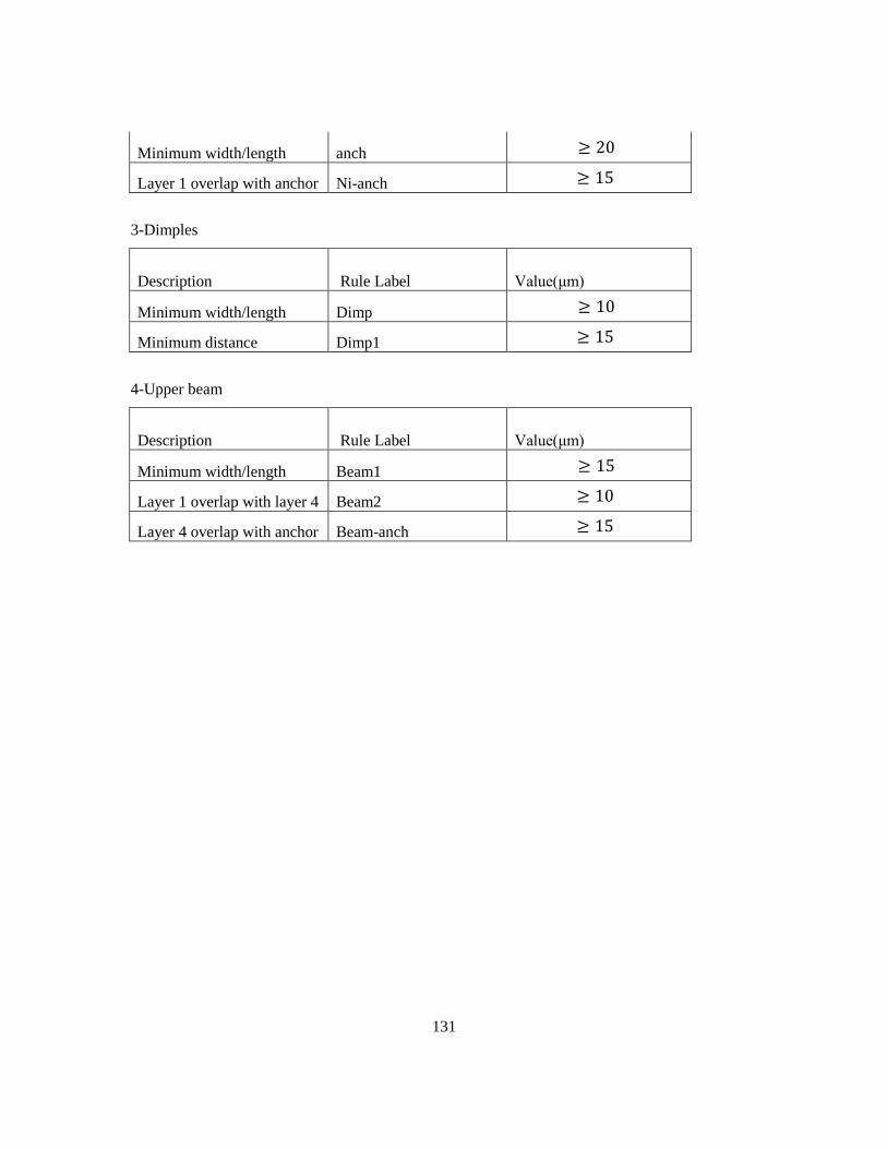
131
Minimum width/length anch
Layer 1 overlap with anchor Ni-anch
3-Dimples
Description Rule Label Value(μm)
Minimum width/length Dimp
Minimum distance Dimp1
4-Upper beam
Description Rule Label Value(μm)
Minimum width/length Beam1
Layer 1 overlap with layer 4 Beam2
Layer 4 overlap with anchor Beam-anch
≥ 20
≥ 15
≥ 10
≥ 15
≥ 15
≥ 10
≥ 15

132
Appendix C
Detailed Microfabrication recipe used for MEMS Reed sensors
1. Create Alumina/Glass/Silicon Superstrate 2.5” square wafers
Naming: #1, #2, #3, #4
2. RCA
o Ratio = 650:130:130 H2O:NH4OH:H2O2
o Temperature = Bubbling!
o Time = 15:00
3. Dehydrate
o Time = 04:00
o Temperature = 120 ⁰C
4. INTLVAC Cr/Au
o 40 nm Cr (e-beam)
o 70 nm Au (e-beam)
5. Mask “L1”
o AZ 3330
FT = 2 µm
Step 1 of 3: 100 RPM for 10 sec.
Step 2 of 3: 500 RPM for 10 sec.
Step 3 of 3: 3000 RPM for 30 sec.
o Soft Bake at 110 ⁰C for 60 sec.
o Exposure:
Intensity at 365 nm = 26 mW.cm-2
Time = 4 sec.
o Post Exposure Bake at 110 ⁰C for 60 sec.
o Develop in AZ 300 MIF for 60 sec.
o Hard Bake at 110 ⁰C for 120 sec.
6. Wet Etch Cr/Au:
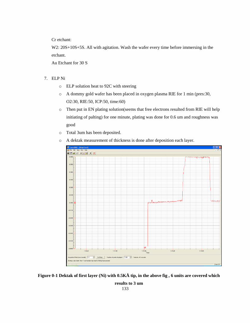
133
Cr etchant:
W2: 20S+10S+5S. All with agitation. Wash the wafer every time before immersing in the
etchant.
Au Etchant for 30 S
7. ELP Ni
o ELP solution heat to 92C with steering
o A dommy gold wafer has been placed in oxygen plasma RIE for 1 min (pres:30,
O2:30, RIE:50, ICP:50, time:60)
o Then put in EN plating solution(seems that free electrons resulted from RIE will help
initiating of palting) for one minute, plating was done for 0.6 um and roughness was
good
o Total 3um has been deposited.
o A dektak measurement of thickness is done after deposition each layer.
Figure 0-1 Dektak of first layer (Ni) with 0.5KÅ tip, in the above fig , 6 units are covered which
results to 3 um

134
8. Gold Electroless
o Heating the solution to 70-75 degree the rate is 25nm per min(2 min I used)
9. Polyimide Preparation W1, W2, W3, W4
o Spinning:
ADD Aluminum Foil
FT = 2.7 µm
Step 1 of 3: 100 RPM for 10 sec.
Step 2 of 3: 500 RPM for 10 sec.
Step 3 of 3: 1300 RPM for 40 sec.
o First Bake at 90 ⁰C for 2:00
o Second Bake at 150 ⁰C for 2:00
o Cure in furnace:
25 ⁰C - 150 ⁰C
Time = 40:00
150 ⁰C - 350 ⁰C
Time = 50:00
350 ⁰C - 350 ⁰C
Time = 30:00
350 ⁰C - 150 ⁰C
Time = 40:00
150 ⁰C - 25 ⁰C
Time = 2:00:00
10. Patterning Anchor
o AZ nLOF 2035
FT = 2.6 µm
Step 1 of 3: 100 RPM for 10 sec.
Step 2 of 3: 500 RPM for 10 sec.
Step 3 of 3: 2500 RPM for 30 sec.
o Soft Bake at 110 ⁰C for 60 sec.
o Exposure:
Intensity at 365 nm = 26 mW.cm-2
Time = 3 sec.

135
o Post Exposure Bake at 110 ⁰C for 60 sec.
o Develop in MIF 300 for 120 sec.
o Hard Bake at 120 ⁰C for 120 sec.
11. Dry Etch PI to pattern anchor
RIE O2 plasma on W1, W3 and W5
o Pressure = 50
o ICP = 150
o RIE = 50
o O2 = 30
o Wafers needed some O2 plasma to clean them from sturdy resist spots
o Time = 30 sec.
o Wafers look BETTER.
12. Dry etch Dimple like step 10
13. Gold Sputtering
Intelvac 0.1um GOLD, SPUTTERING
14. Final mask patterning
15. Wet etch gold 25 Sec
16. ELP Ni for 3 min
17. ELP Gold for 2 min
18. PR coating BEFORE dicing
o Spin AZ 3330 using 500 RPM for 15 sec. then 2000 RPM for 45 sec.
o Bake at 110⁰C for 3 min.
19. EKC of devices
o 30 min. (more than 20 min. to guarantee the release)
o 60 C
20. IPA of W3 devices
o Total time = 3*8:00 min.
21. CO2 CPD of devices
o The whole chamber, glass, carrier and lid are cleaned with IPA
o A new cylinder is being used
o 4 different designs of W3 devices are inside the chamber for CPD release

136
o CPD process was successful

137
Bibliography
[1] J. Lenz and A. S. Edelstein (2006), “Magnetic Sensors and Their Applications”, IEEE Sensors
Journal, 6(3), pp. 631-649.
[2] P. Ripka (2001). Magnetic Sensors and Magnetometers. Artech House, Norwood, MA.
[3] R. L. Fagaly (2006), “Superconducting quantum interference device instruments and
applications”, Rev. Sci. Instrum., 77, pp. 101-145.
[4] L. D. Landau and E. M. Lifshitz (1960). Electrodynamics of Continuous Media. Pergamon Press,
Oxford.
[5] G. T. Rado and V. J. Folen (1961), “Observation of the Magnetically Induced Magnetoelectric
Effect and Evidence for Antiferromagnetic Domains”, Phys. Rev. Lett., 7, pp. 310-311.
[6] R. Ramesh and N. A. Spaldin (2007), “Multiferroics: progress and prospects in thin films”,
Nature Mater, 6, pp. 21-29.
[7] W. Eerenstein, N. D. Mathur, and J. F. Scott (2006) “Multiferroic and magnetoelectric
materials”, Nature, 442, pp. 759-765.
[8] S. De and N. Aluru, “A hybrid full-Lagrangian technique for the static and dynamic analysis of
magnetostatic MEMS”, Journal of Micromechanics and Microengineering, 16 (2006) 2646-2658.
[9] M. Tang, Y. Lee, R. Kumar, R. Shankar, and O. Neel, “A MEMS Micro-Reed Switch Designed
for Portable Applications”, Transducers’11, Beijing, China, June 5-9, 2011.
[10] M. Tang, E. Liao, Ch. Cheng, D. Lee,Y. Lee, R. Kumar, R. Shankar, O. Neel, G. Noviello, and
F. Italia, “A Magnetostatic MEMS Switch Designed for Portable Applications”, Journal Of
Microelectromechanical Systems, Vol. 19, No. 5, October 2010.
[11] S. Marauska, R. Jahn, H. Greve, E. Quandt, R. Knochel, and B. Wagner, “ MEMS magnetic field
sensor based on magnetoelectric composites”, Journal of Micromechanics and Microengineering,
Vol. 22, No. 6.
[12] M. Tang, E. Liao, Ch. Cheng, D. Lee,Y. Lee, R. Kumar, R. Shankar, O. Neel, G. Noviello, and
F. Italia, “A MEMS Microreed Switch with One Reed Embedded in the Silicon Substrate”, JMEMS,
Vol. 20, Issue 6.

138
[13] H. Yanga, N. Myung, J. Yeea, Y. Park, B. Yoob, M. Schwartz, K. Nobe, and J. Judya,
“Ferromagnetic micromechanical magnetometer”, Sensors and Actuators, 2002, Vol. 97.
[14] D. DiLellaa, L. J. Whitmana, R. J. Coltona, and T. W. Kenny, “A micromachined magnetic-field
sensor based on an electron tunneling displacement transducer”, Sensors and Actuators, 2000, Vol.
86.
[15] R. B. Givens, J. C. Murphy, R. Osiander, T. J. Kistenmacher, and D. K. Wickenden, “A high
sensitivity, wide dynamic range magnetometer designed on a xylophone resonator”, Applied Physics
Letter, 1996, Vol. 96.
[16] A. S. Edelstein and G. A. Fischer, “Minimizing 1/f noise in magnetic sensors using a
microelectromechanical system flux concentrator”, J. Appl. Phys., Vol. 91, pp. 7795-7797, 2002.
[17] H. H. Gatzen, E. Obermeier, T. Kohlmeier, T. Budde, H. D. Ngo, B. Mukhopadhya, and M. Farr
2003, “An electromagnetically actuated bi-stable MEMS optical microswitch”, Int. Conf. on Solid-
State Sensors and Actuators: Transducers, pp. 1514-7.
[18] Z. Nami, C. H. Ahn, and M. G. Allen, 1996, “An energy-based design criterion for magnetic
microactuators”, J. Micromech. Microeng. 6 337-44.
[19] A. Frangi, P. F. Ragani, and L. Ghezzi, 2005, “Magneto-mechanical simulations by a coupled
fast multipole method-finite element method and multigrid solvers”, Comput. Struct. 83 718-26.
[20] A. Nicolet, F. Delince, A. Genon, and W. Legros, 1992, “Finite elements-boundary elements
coupling for the movement modeling in two dimensional structures”, J. Physique III 2 2035-44
[21] M.-H. Phan and H.-X. Peng. Progress in Materials Science. 53 (2008) 323-420.
[22] J. E. Lenz, “A review of magnetic sensors”, Proc IEEE 1990;78:973-89.
[23] T. Meydan. Application of amorphous materials to sensors. J Magn Magn Mater 1995;133:525-
32.
[24] P. Ripka, “Magnetic sensors and magnetometers”, Artech House Publishers, 2001.
[25] L. V. Panina and K. Mohri. Magneto-impedance effect in amorphous wires. Appl Phys Lett
1994;65:1189-91.
[26] L. V. Panina, K. Mohri, T. Uchiyama, and M. Noda. Giant magneto-impedance in Co-rich
amorphous wires and films. IEEE Trans Magn 1995;31:1249-60.
[27] M. Vazquez and A. Hernando. A soft magnetic wire for sensor applications. J Phys D: Appl Phys
1996;29:939-49.
[28] H. Chiriac and T. A. Ovari. Amorphous glass-covered magnetic wires: preparation, properties,
applications. Prog Mater Sci 1996;40:333-407.

139
[29] M. Vazquez. Giant magnetoimpedance in soft magnetic ‘‘wires’’. J Magn Magn Mater
2001;226-230:693-9.
[30] M. Knobel and K. R. Pirota. Giant magnetoimpedance: concepts and recent progress. J Magn
Magn Mater 2002;242-245:33-40.
[31] M. Knobel, M. Vazquez, and L. Kraus. Giant magnetoimpedance. In: Buschow KH, editor.
Handbook of magnetic materials, Vol. 15. Amsterdam: Elsevier Science B.V.; 2003. pp. 1-69
[Chapter 5].
[32] L. Kraus. GMI modeling and material optimization. Sens Acta A 2003;106:187-94.
[33] C. Tannous and J. Gieraltowski. Giant magneto-impedance and its applications. J Mater Sci:
Mater Electro 2004;15:125-33.
[34] K. Mohri, T. Kohsawa, K. Kawashima, H. Yoshida, and L. V. Panina. Magneto-inductive effect
(MI effect) in amorphous wires. IEEE Trans Magn 1992;28:3150-2.
[35] D. Menard, M. Britel, P. Ciureanu, and A. Yelon. Giant magnetoimpedance in a cylindrical
magnetic conductor. J Appl Phys 1998;84:2805-14.
[36] A. Yelon, D. Menard, M. Brittel, and P. Ciureanu. Calculations of giant magnetoimpedance and
of ferromagnetic resonance response are rigorously equivalent. Appl Phys Lett 1996;69:3084-5.
[37] L. V. Panina and K. Mohri, “Magneto-Impedance in Multilayer Films”, 2000, Sensors and
Actuators A, Vol. 81, 71-76.
[38] T. Morikawa, Y. Nishibe, H. Yamadera, Y. Nonomura, M. Takeuchi, and Y. Taga, “Giant
Magneto-Impedance Effect in Layered Thin Films”, IEEE Transactions on Magnetics, Vol. 33, 1997.
[39] Z. Ren, F. Bouillault, A. Razek, and J. C. Verite, “Comparison of different boundary integral
formulations when coupled with finite elements in three dimensions”, IEE Proc., 1988, 135 501-7.
[40] Y. Hui, T. X. Nan, N. X. Sun, and M. Rinaldi, (2013, January). MEMS resonant magnetic field
sensor based on an AlN/F e G a B bilayer nano-plate resonator. In Micro Electro Mechanical Systems
(MEMS), 2013 IEEE 26th International Conference on (pp. 721-724). IEEE.
[41] C. I. Chang, M. H. Tsai, C. M. Sun, and W. Fang, (2014). Development of CMOS-MEMS in-
plane magnetic coils for application as a three-axis resonant magnetic sensor. Journal of
Micromechanics and Microengineering, 24(3), 035016.
[42] S. Park, M. S. Al-Ghamdi, M. Khater, E. Abdel-Rahman, and M. Yavuz, (2014, August).
Adjustable Sensitivity MEMS Magnetic Sensor. In ASME 2014 International Design Engineering
Technical Conferences and Computers and Information in Engineering Conference (pp.
V004T09A016-V004T09A016). American Society of Mechanical Engineers.

140
[43] S. Gudoshnikov, N. Usov, A. Nozdrin, M. Ipatov, A. Zhukov, and V. Zhukova, (2014). Highly
sensitive magnetometer based on the off‐diagonal GMI effect in Co‐rich glass‐coated
microwire. physica status solidi (a), 211(5), 980-985.
[44] S. NazariNejad, A. Akhavan Fomani and R. Mansour, 'Giant Magneto-Impedance Thin Film
Magnetic Sensor', IEEE Transactions on Magnetics, vol. 49, no. 7, pp. 3874-3877, 2013.
[45] S. NazariNejad, A. A. Fomani, & R. R. Mansour “Multilayer Giant Magneto-Impedance sensor
for low field sensing”, IEEE SENSORS 2013, IEEE (pp. 1-4). November 2013.
[46] F. Barazandeh, S. NazariNejad, R. Nadafi, A. MehdiAbadi and Z. Ghasemi, 'Design and
microfabrication of a compliant microgripper using nonbrittle and biocompatible material',
Proceedings of the Institution of Mechanical Engineers, Part C: Journal of Mechanical Engineering
Science, vol. 227, no. 12, pp. 2886-2896, 2013.
[47] M. Hajhashemi, F. Barazandeh, S. Nejad and R. Nadafi DB, 'Design and microfabrication of a
constant-force microgripper', Proceedings of the Institution of Mechanical Engineers, Part C:
Journal of Mechanical Engineering Science, vol. 225, no. 11, pp. 2739-2748, 2011.
[48] R. Nadafi DB, S. Nazari Nejad, M. Kabganian and A. Dinparast Djadid, 'Adaptive control of a
legged capsular microrobot based on Lyapunov stability criteria', Proceedings of the Institution of
Mechanical Engineers, Part C: Journal of Mechanical Engineering Science, vol. 226, no. 4, pp. 887-
899, 2011.
[49] H. Parsaiyan, F. Barazandeh, S. Nazari Nejad, S. Rezaei, M. Kabganian, M. Parsaiyan and M.
Safdari, 'Theoretical and experimental study of a novel microfabricated fibrillar structure',
Proceedings of the Institution of Mechanical Engineers, Part L: Journal of Materials: Design and
Applications, vol. 224, no. 4, pp. 199-207, 2010.
[50] Reza Nadafi, D. B., S. N Nejad, M. Kabganian, & F. Barazandeh, (2010, May). “Neural network
calibration of a semiconductor metal oxide micro smell sensor” , Test Integration and Packaging of
MEMS/MOEMS (DTIP), 2010 Symposium on (pp. 154-157). IEEE.
[51] R. Nadafi, F. Edalatfar, P. Zomorodian, S. N. Nejad, M. Kabganian, & F. Barazandeh, "A
comparative design study on in-pipe inspection micro robots using AHP method." Design Test
Integration and Packaging of MEMS/MOEMS (DTIP), 2010 Symposium on. IEEE, 2010.
[52] N. Sayyaf, F. Barazandeh, S. N. Nejad, & M. R. Razfar, (2009, December). Design and
Fabrication of a Novel Micro Angle Sensor. In 2009 Fifth International Conference on MEMS
NANO, and Smart Systems (pp. 37-40). IEEE.

141
[53] C. Dong; S. Chen; T. Y. Hsu, "A simple model of giant magneto-impedance effect in amorphous
thin films." Journal of magnetism and magnetic materials 250 (2002): 288-294.
[54] E. Costa Silva; L. Gusmão; L. Hall; E. Costa Monteiro, “Magnetic field transducers based on the
phase characteristics of GMI sensors and aimed at biomedical applications”, 13TH International
Conference on Biomedical Engineering, 2009, Singapore.
[55] A. García-Arribas; J. M. Barandiaran; D. De Cos, (2008), Finite element method calculations of
GMI in thin films and sandwiched structures: size and edge effects. Journal of Magnetism and
Magnetic Materials, 320(14), e4-e7.
[56] L. Kraus, "GMI modeling and material optimization." Sensors and Actuators A: Physical 106.1
(2003): 187-194.
[57] B. Li and J. Kosel, 'Optimized 425MHz passive wireless magnetic field sensor', 2014 IEEE
MTT-S International Microwave Symposium (IMS2014), 2014.
[58] R. Popovic, & H. P. Baltes, (1987). U.S. Patent No. 4,700,211. Washington, DC: U.S. Patent
and Trademark Office.