minatec and cea-tech : at the core of the french ... · semiconductor materials for extreme...
TRANSCRIPT

| PAGE 1CEA | 10 AVRIL 2012NIMS WeekOct.20th, 2016
MINATEC and CEA-Tech :
At the core of the French
innovation hub of Grenoble
Jean-Charles GUIBERT,Director of Technology Transfer, CEA
Director of MINATEC

HIGH LEVEL FORUM 2016@GRENOBLE M. SUMIKAWA
The Policy Speech by Prime Minister Shinzo Abe
as of January 22, 2016
The Policy Speech by Prime Minister Shinzo Abe
as of January 22, 2016
Governmental Policy for Innovation
To foster innovation ~from basic research
to practical use and commercialization~
Open Innovation!
The most innovation friendly country
in the world
• 5th Science and Technology Basic Plan (2016-2020)- Council for Science, Technology and Innovation
2

3
MilitaryApplications
Division
Nuclear EnergyDivision
TechnologicalResearch Division
Mission DAM : France’s national security independence
Mission DEN : France’s energy independence
Mission DRT : French business’ economic competitiveness
CEA : Worldwide leader in technological research

SUMMARY
| PAGE 4Direction de la Valorisation
• The RTO model (Research Technological Organization)
• CEA, the French RTO
• MINATEC the Grenoble Innovation Campus
• Conclusion

5
GAP
Pump primingwith academics
5–10 years
Technology transferwith industry
1–3 years
the French RTO to bridge the gap between research and industry

6
Research Technological Organizations (RTO) :
A key structure in the research tool box of governments
Research leads to invention
Industry leads to products
Who cares of innovation ?
RTO mission isto bridge, to fill in the gap
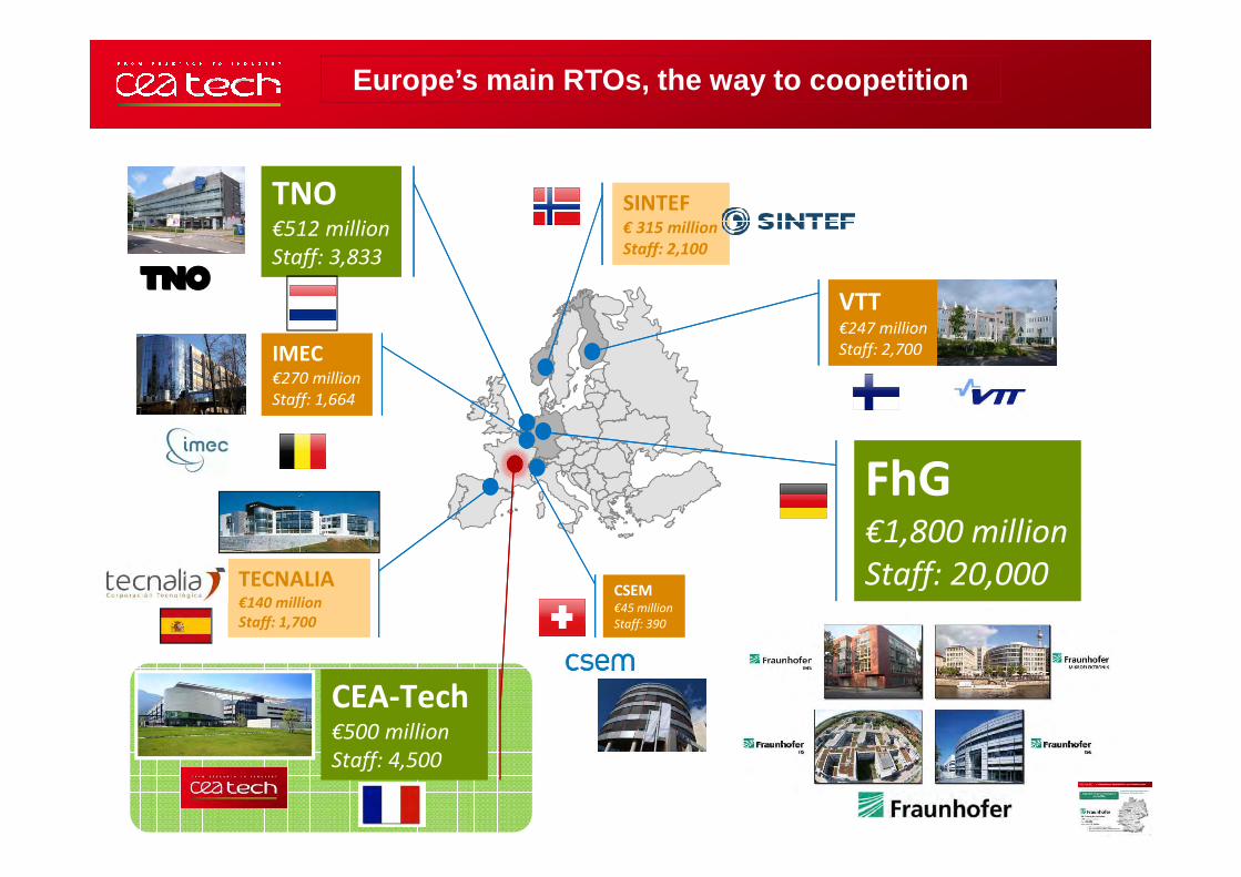
Europe’s main RTOs, the way to coopetition
7
IMEC€270 million
Staff: 1,664
CSEM€45 million
Staff: 390
VTT€247 million
Staff: 2,700
TECNALIA€140 million
Staff: 1,700
SINTEF€ 315 million
Staff: 2,100
TNO€512 million
Staff: 3,833
FhG€1,800 million
Staff: 20,000
CEA-Tech€500 million
Staff: 4,500

CEA | Benchmark CEA Tech | 20 Janvier 2016
32% 27%40%
19%
35%
15%
28%32%
17% 28%
15%
8% 8% 8%
6%
13%
17%
32% 34% 36%
75%
24%
53%
0%
10%
20%
30%
40%
50%
60%
70%
80%
90%
100%
Funding mix 2014
Industrial funding
European funding
National public funding
Base funding
EUROPEAN RTOs – Funding benchmark
| PAGE 8
On long term, RTO funding equilibrium model : 1/3 Base, 1/3 Public competitive, 1/3 Industry

CEA | Benchmark CEA Tech | 20 Janvier 2016 | PAGE 9CSEM
IMEC
TNO
SANDIANREL
KAIST
NIMS / AIST
ITRI
A-STARFZK
FhG
Selection of centres for benchmark analysis
CNSI
JPL/CALTECH
Nth Carolina.
Georgia Tech.
MIT.
CATAPULTBOMBAY
OIST
ALBANY
NANOPOLIS
TECHNION

SUMMARY
| PAGE 10Direction de la Valorisation
• The RTO model (Research Technological Organization)
• CEA, the French RTO
• MINATEC the Grenoble Innovation Campus
• Conclusion

11
MilitaryApplications
Division
Nuclear EnergyDivision
TechnologicalResearch Division
Mission DAM : France’s national security independence
Mission DEN : France’s energy independence
Mission DRT : French business’ economic competitiveness
CEA : Worldwide leader in technological research

4 octobre
| PAGE 12Direction de la Valorisation
Ranking of the world most innovative research institutio ns
Thomson Reuters : CEA is topping the list thanks to its tech transfer and IP strategy
1 - CEA Score : 206 France2 - Fraunhofer Society Score: 202 Germany
3 - Japan Science & Technology Agency Score: 201 Japan
4 - U.S. Department of Health & Human Services Score: 193 USA
5 - National Center for Scientific Research Score: 189 France
6 - Korea Institute of Science & Technology Score: 183 South Korea
7 - National Institute of Advanced Industrial Science & Technology Score: 182 Japan
8 - U.S. Department of Energy Score: 179 USA
9 - Agency for Science, Technology & Research Score: 175 Singapore10 - French Institute of Health & Medical Research Score: 175 France
11 - Helmholtz Association Score: 157 Germany
12 - U.S. Department of Veterans Affairs Score: 157 USA
13 – RIKEN Score: 146 Japan
14 - National Research Council Canada Score: 139 Canada
15 - Max Planck Society Score: 137 Germany
16 - Chinese Academy of Sciences Score: 135 China
17 - Pasteur Institute International Network Score: 135 France
18 - National Institute for Materials Science Score: 132 Japan
19 - United States Navy Score: 123 USA
20 - Commonwealth Scientific & Industrial Research Organisation Score: 119 Australia
21 - Spanish National Research Council Score: 114 Spain
22 - Academia Sinica Score: 106 Taiwan
23 - United States Army Score: 100 USA
24 - National Aeronautics and Space Administration Score: 99 USA
25 - Russian Academy of Sciences Score: 98 Russia
“Silicon Valley’s hoodie-wearing techentrepreneurs are the poster kids ofinnovation. But the innovators who arereally changing the world are more likely towear labcoats and hold government-relatedjobs in Grenoble, Munich or Tokyo.”
Direction de la Valorisation
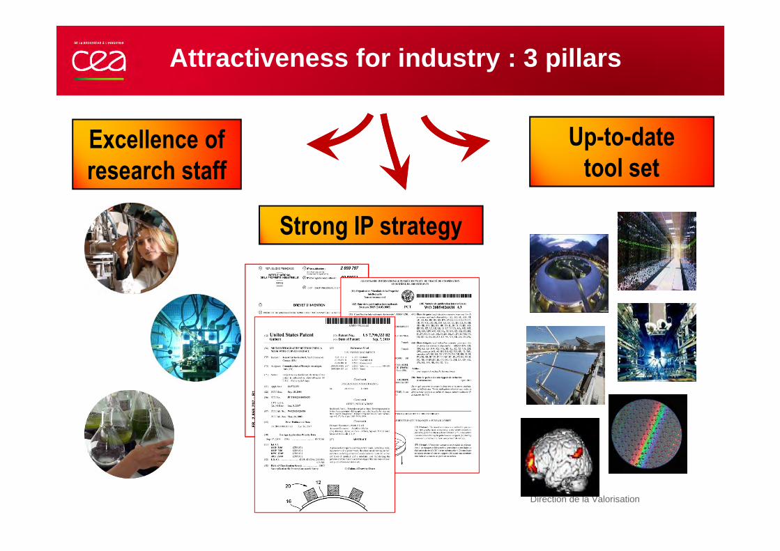
Attractiveness for industry : 3 pillars
Excellence of
research staff
Strong IP strategy
Up-to-date
tool set

BUSINESS MODEL OF RESEARCH FOR CEA
| PAGE 14Direction de la Valorisation
Excellence of staff
in research labs
R&D for industry and agencies
and subsequent Licensing
Spin-off strategy
IP portfolio generation
IP EXPLOITATION
through contracted research« mid-long term industrial partner » « new industrial partner»

300 mm clean room
The Leti silicon platform for nanoelectronics
Information
| PAGE 15

The LETI MEMS 200 platform
Information
16
200 mm clean room
The Leti silicon platform for N&MEMS

Access to large
research facilities
Characterization platform
~80 Researchers and Technicians,40 Principal characterization tools,2,500m2 of laboratories,3,5 � million of investments per year,7 Centers of expertise

18
MANUFACTURING

Architectures and systems-on-chip
> Manycore processor
> Safe RT OS
> IC Architecture
> IC & SOC simulation
> Imaging
> EMC / RF Reliability
> Smart Sensors
Systems engineering tools
> Green IT
> Wire diagnostic
> Pedestrian detection
> Vision-based geolocation
> Safe command-control
> Hardened camera
> Energy management
2626-2
Safety, reliability, and standards
Embedded systems

The batteries platform
| 20
Energy

NANOMATERIALS ARE STRATEGIC FOR THE PERFORMANCES OF THE COMPONENTS FOR LOW CARBON ENERGY
| PAGE 21
LWR GEN IV Fusion
ElectrochemicalStorage Hydrogen Solar
Ene
rgy
Effi
cien
cy&
Har
vest
ing
Nuc
lear
Ene
rgy
Alte
rnat
ive
Ene
rgie
s

NEW NANOCOMPOSITES FOR SUPERCAPACITORS THROUGHAEROSOL CVD OF VERTICALLY ALIGNED CNT
| PAGE 22
Transport, electronic, applications for unique use, …
Different fields of applications
� Time constant : few seconds - few minutes
Supercapacitors
- Electrodes, electroactive materials- Electrolyte
� Performances depends on their components :

PROCESS UPSCALING
Production on large silicon wafers : 300 mm diameter
P. Boulanger et al., Journal of Physics: Conference Series429, 012050 (2013)
E=100µm
V=6µm/min
707 cm2
Optimization in progress: increase of homogeneity in thickness and of growth rate
| PAGE 23

24
Up-scaled High QualityVACNT Growth
Conformal ECP coating
Creation of a start-upP. BoulangerApril 2013
Targeted market : next generation of supercapacitors based on VACNT-engineered electrodes
License agreement between CEA and NaWa : 4 patents
VALORIZATION AND TECHNOLOGY TRANSFER
Electrodes exhibiting
promising properties=
New concept of supercapacitorsContinuous and low
cost process
| PAGE 24
| 25
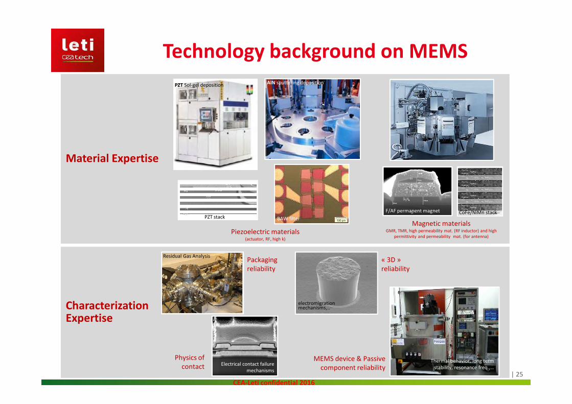
Technology background on MEMS
CharacterizationExpertiseCharacterizationExpertise
Packaging
reliability
Residual Gas Analysis
Physics of
contact Electrical contact failure
mechanisms
« 3D »
reliability
electromigrationmechanisms,..
MEMS device & Passive
component reliabilityThermal behavior, long term
stability, resonance freq.,…
Material ExpertiseMaterial Expertise
Piezoelectric materials(actuator, RF, high k)
Magnetic materials GMR, TMR, high permeability mat. (RF inductor) and high
permittivity and permeability mat. (for antenna)
PZT Sol-gel depositionAlN sputtering deposition
F/AF permanent magnet
BAW filter
CoFe/NiMn stackPZT stack
CEA-Leti confidential 2016
| 26
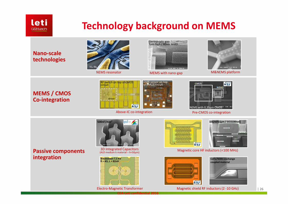
Technology background on MEMS
MEMS / CMOSCo-integrationMEMS / CMOSCo-integration
Above-IC co-integration
NEMS with 0.35µm CMOS
driver
RF switch on top of CMOS circuit
GMR sensor on top of CMOS circuit
Pre-CMOS co-integration
Nano-scaletechnologiesNano-scaletechnologies
M&NEMS platformNEMS resonator MEMS with nano-gap
Electrostatic gap:3µm high / 80nm width
Passive componentsintegrationPassive componentsintegration
500nF/mm²
3D Integrated Capacitors(ALD medium k material – h=50µm)
Magnetic core HF inductors (<100 MHz)
Magnetic shield RF inductors (2 -10 GHz)
CoFe/NiMn exchange
coupled material
10x[NiFe1µm / SiO2100nm]
Electro-Magnetic Transformer
Breakdown 7,5 KV R ≈ 4Ω, L ≈ 82nH
CEA-Leti confidential 2016
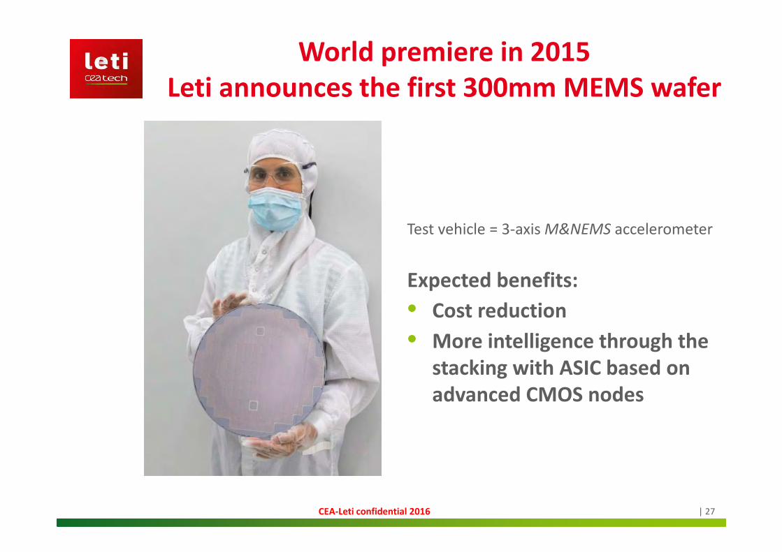
| 27
World premiere in 2015
Leti announces the first 300mm MEMS wafer
Test vehicle = 3-axis M&NEMS accelerometer
Expected benefits:
• Cost reduction
• More intelligence through the
stacking with ASIC based on
advanced CMOS nodes
CEA-Leti confidential 2016

SUMMARY
| PAGE 28Direction de la Valorisation
• The RTO model (Research Technological Organization)
• CEA, the French RTO
• MINATEC the Grenoble Innovation Campus
• Conclusion

MINATEC – June 2014Page 29
MINATECinnovation campus

MINATEC® 2015 - Jean-Charles Guibert – Director of MINATEC ®
Systems for biology & health
Smart systems, Telco, IT design
Microelectronics on silicon
Microsystems on silicon
Optoelectronics components
Technology research on micro and nanotechnologies
Research & Technology
Institute founded in 1967
Director : Dr Marie-Noëlle Semeria
1700 collaborators250+ PhD & post-docs
40 nationalities
2200 patent families40 % under licensing
300+ industry partners
50 start-ups
8 000m² clean roomsFor 200 and 300mm wafer fab, operated 24/7
CEA-Leti institute is the heart of MINATEC campus

MINATEC® 2015 - Jean-Charles Guibert – Director of MINATEC ®
2,400 people
560 PhDs & post-docs
� Interdisciplinarity
� Creativity
� Technology transfer
Research
1,400 people
� Attractivity
� Skills for the future
Education
MINATEC campus based on the triple helix concept : Education – Research - Industry
600 people
� Technology transfer
� Industrial partnerships
� Jobs creation
Industry
� >3000 research staff
� >1000 students
� Annual Budget 350 M€
Industry & contracts >60%
� 13 000m² cleanrooms
� 400 graduates MS/PhD
� 1600 scientific publications /year
� 400 new patents /year
� 20 joint laboratories
� 10 start-up /year
� Operated by the
joint labs
Start-ups

MINATEC® 2015 - Jean-Charles Guibert – Director of MINATEC ®
MINATEC® campus – from labs to shared platforms
TTO

MINATEC® 2015 - Jean-Charles Guibert – Director of MINATEC ®
1 official delegation weekly to discover our campus
International official delegations
• 2015 : 40 delegations received to visit
MINATEC campus
• from 20 nationalities
• > 40 000 visitors in 2015
• 126 events
• 627 meetings
They visited MINATEC in 2016
Yoichi SUZUKI, Japan Ambassador
Najat VALLAUT-BELCKACEM, French Minister for Higher Education & Research
Yuko HARAYAMA, Japan Prime Minister cabinet office, executive member of the council for science, technology and innovation
Hiroshi AMANO, 2014 Nobel Prizein Physics Nogoya University

MINATEC® 2015 - Jean-Charles Guibert – Director of MINATEC ®
MINATEC / JAPAN relationship highlights
2014/10 : MoU NIMS-GIANT - 2 offices opened in Grenoble (1 in MINATEC) 1 in Tsukuba to host researchers� 3 Tsukuba University’ students in internships in MINATEC Leti’s labs in 2015
- 2014/09 : MoU KEIO-CEA-CNRS on micro- and nano-technologies� 3 students in internship in MINATEC Leti’s labs in 2015
- 2014/07 : Hirofumi NAKASONE, visit Member of the House of Councillors of Japan
- 2014/10 : Hiroshi AMANO, 2014 Nobel Prize in Physics announcement in MINATEC – working with Aledia r&d team

MINATEC® 2015 - Jean-Charles Guibert – Director of MINATEC ®
Large part of MINATEC activity isdedicated to develop science and
technology and transfer to industry or create future industry through start-up

MINATEC® 2015 - Jean-Charles Guibert – Director of MINATEC ®
/. 1972- Leti EFCIS/. 1982 : EFCIS absorbed by THOMSON/.Created as SGS-THOMSON Microelectronics in June 1987, from merger of SGS Microelettronica (Italy) and Thomson Semiconducteurs (France)/. Renamed STMicroelectronics in May 1998
(Etude et Fabrication de Circuits Intégrés Spéciaux)
• Among the world’s largest semiconductor companies
• A leading Integrated Device Manufacturer serving all electronics segments
• A leading technology innovator ( around 8,700 R&D researchers, ~24,000 patents)
• Key strengths in Multimedia Convergence, Power Applications and Sensors
• Rich, balanced portfolio (ASICs, Application-Specific Standard Products and Multi-Segment Products)
• A pioneer and visionary leader in sustainability
A world leader in providing the semiconductor solutions
• Approximately 45,000 employees including ST-Ericsson (Dec.31, 2014)
• 2014 revenue: $7.40 billion
• Advanced R&D centers in 10 countries&11 main manufacturing sites
• Corporate Headquarters: Geneva, Schwtz
• Global presence with sales offices all around the world
• Public since 1994 - shares traded on New York Stock Exchange (NYSE: STM), Euronext Paris, and Borsa Italiana
STMicroelectronics // A world leader in providing the semiconductor solutions
MINATEC® 2015 - Jean-Charles Guibert – Director of MINATEC ®
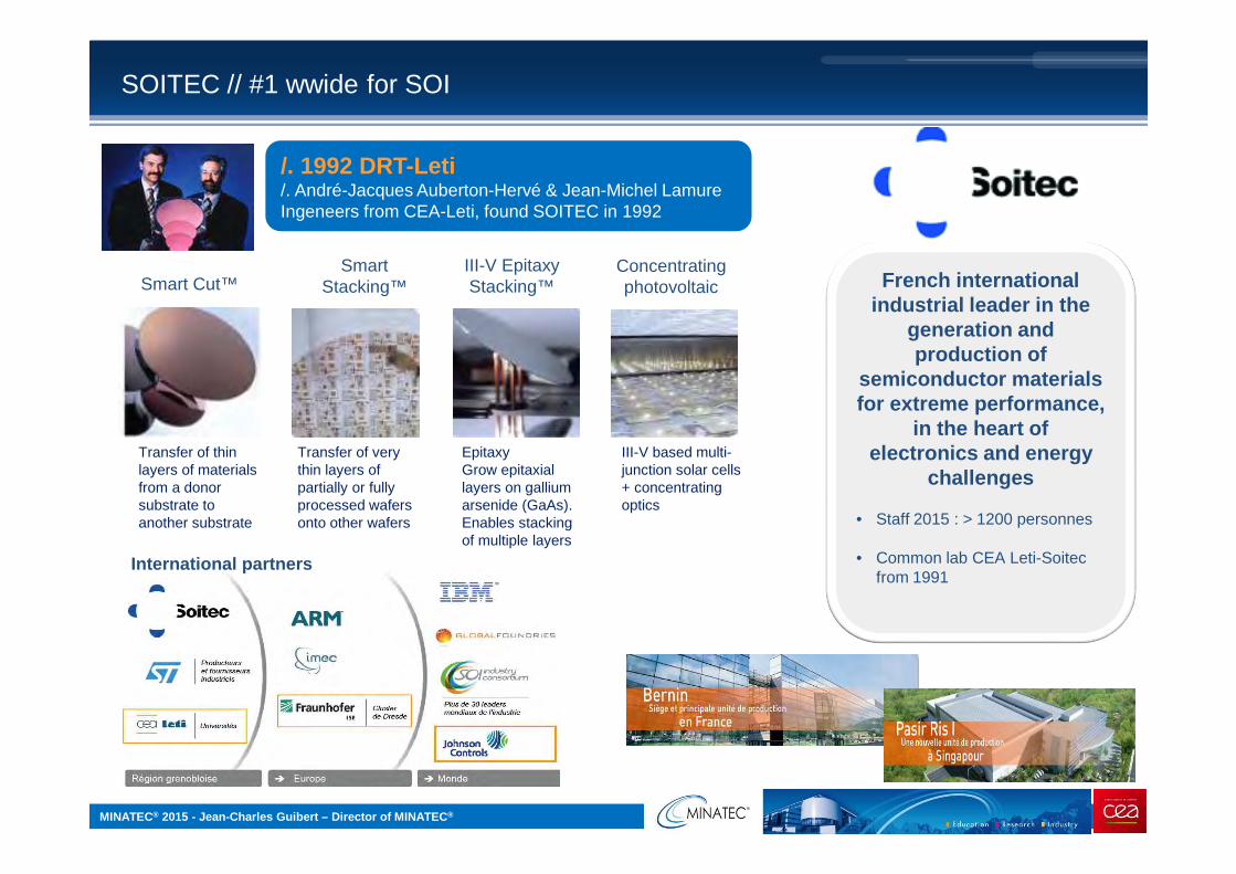
Smart Cut™III-V EpitaxyStacking™
Concentratingphotovoltaic
International partners
French international industrial leader in the
generation and production of
semiconductor materials for extreme performance,
in the heart of electronics and energy
challenges
• Staff 2015 : > 1200 personnes
• Common lab CEA Leti-Soitecfrom 1991
/. 1992 DRT-Leti/. André-Jacques Auberton-Hervé & Jean-Michel LamureIngeneers from CEA-Leti, found SOITEC in 1992
Smart Stacking™
Transfer of thin layers of materials from a donor substrate to another substrate
Transfer of very thin layers of partially or fully processed wafers onto other wafers
EpitaxyGrow epitaxial layers on gallium arsenide (GaAs).Enables stacking of multiple layers
III-V based multi-junction solar cells + concentrating optics
SOITEC // #1 wwide for SOI
MINATEC® 2015 - Jean-Charles Guibert – Director of MINATEC ®
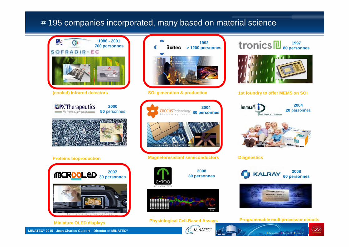
1986 - 2001700 personnes
200050 personnes
200730 personnes
1992> 1200 personnes
200480 personnes
200830 personnes
199780 personnes
200420 personnes
200860 personnes
(cooled) Infrared detectors SOI generation & production 1st foundry to offer MEMS on SOI
Proteins bioproduction Magnetoresistant semiconductors Diagnostics
Miniature OLED displays Physiological Cell-Based Assays Programmable multiprocessor circuits
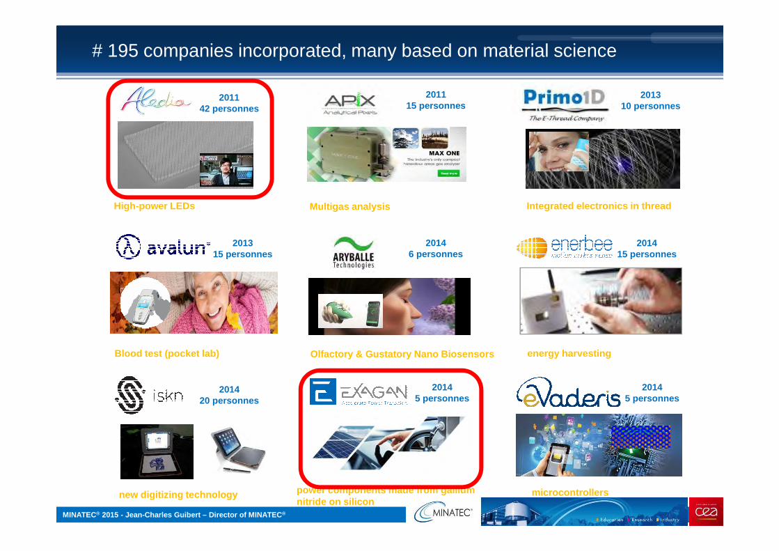
# 195 companies incorporated, many based on material science
MINATEC® 2015 - Jean-Charles Guibert – Director of MINATEC ®
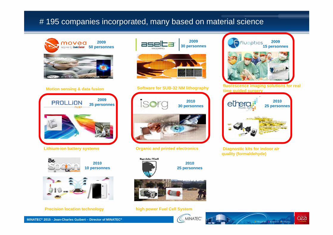
201030 personnes
200915 personnes
200950 personnes
200930 personnes
200935 personnes
201025 personnes
201010 personnes
201025 personnes
Motion sensing & data fusion Software for SUB-32 NM lithography fluorescence imaging solutions for real time guided surgery
Lithium-ion battery systems Organic and printed electronics Diagnostic kits for indoor air quality (formaldehyde)
Precision location technology high power Fuel Cell System
# 195 companies incorporated, many based on material science
MINATEC® 2015 - Jean-Charles Guibert – Director of MINATEC ®
201415 personnes
201310 personnes
201315 personnes
201420 personnes
201142 personnes
201115 personnes
20146 personnes
20145 personnes
20145 personnes
High-power LEDs Multigas analysis Integrated electronics in thread
Blood test (pocket lab) Olfactory & Gustatory Nano Biosensors energy harvesting
new digitizing technology power components made from gallium nitride on silicon
microcontrollers
# 195 companies incorporated, many based on material science

SUMMARY
| PAGE 41Direction de la Valorisation
• The RTO model (Research Technological Organization)
• CEA, the French RTO
• MINATEC the Grenoble Innovation Campus
• Conclusion
MINATEC® 2015 - Jean-Charles Guibert – Director of MINATEC ®
Vision and mission � cultural change
� Vision �have to be supported by politics and top management� focus on cultural change (ie public research favorize
employment….in private industry) � results only on long term � will not be seen at the timing
of political agendas ! �Comprehensive by all citizens
� Mission �daily job of middle management to focus on impact�explain why and how public salaries are paid !�Short / middle term oriented�Dedication of all research staff�Benchmark : programs, organization, costs, investment,..

MINATEC® 2015 - Jean-Charles Guibert – Director of MINATEC ®
The 3 pillars of attractivty
� Research staff platform � how much ? Permanent staff ? engineers, technicians, PhD ? International ? Master students available on site ?
� Equipments platform � Investment capacity along last years? Wwide unique ? Maintenance ? 24/7 operation for industry support ? Sharing costs with start-up ?
� Intellectual property platform � Investment capacity along last years? portfolio size ? In-house dedicated staff ? Strong management strategy ? Seen as an advertising tool or as a cost ?

MINATEC® 2015 - Jean-Charles Guibert – Director of MINATEC ®
The 3 requests from customers
� How to achieve customer goals � Project management ? Reporting ? ISO certified ? Results guaranteed ? SWOT analysis culture ?
� Business model � existing one ? Full cost per person per activity per year ? How much to cover for the customer : 50, 80, 100, 120 % ? Same cost for national and international customers ?
� Intellectual property access � Background access included in program cost ? Foreground proprietary rules ? Licence fee calculation ? Rules for exclusive or non exclusive licence ?
MINATEC® 2015 - Jean-Charles Guibert – Director of MINATEC ®
� International visibility � are you in premier league ? Do international rankings have a real impact ? and is your center attractive enough for the best students, researchers, industry, investors?
� Ecosystem generation and development � strength and commitment of collaborations and interactions between the different entities from education, research and industry ? Are you contributing to new research model generation ?
� Economic impact � to estimate per year, on your research area ? who is able to calculate? Who cares of precise datas ? Advertising tool or guideline for authorities ?
The 3 high level KPI (Key Performance Indicators)

46
Thank you, http://www.minatec.org/ja/