mikroniek_2008-3 - dspe
TRANSCRIPT

P R O F E S S I O N A L J O U R N A L O N P R E C I S I O N E N G I N E E R I N G V O L U M E 4 8 - I S S U E 3
Picometre metrology in space • Thermo-mechanical precision design
Optical strain gauge • Smallest laser ever • Configurable Slit Unit
Flexure-based active mirror support • 3D measurement of micro-components
Workpiece touch probes • Active damping • Wafer measuring machine
MIKRONIEK IS A PUBLICATION OF THE DUTCH SOCIETY OF PRECISION ENGINEERINGWWW.PRECISIEPORTAAL.NL
SPECIAL ISSUEOn the occasion of the Summer School Opto-mechatronicsEindhoven, the Netherlands30 June - 4 July 2008
00_Omslag_nr3_2008.indd 100_Omslag_nr3_2008.indd 1 06-06-2008 12:06:3806-06-2008 12:06:38

Within the Business Unit Advanced Precision and Production Equipment(APPE) precision technology is a familiar term. What about a highlyaccurate spectrometer that orbits in space for many years in extremeconditions and can continue to spot the polluted air in your back garden? Or the very latest inspection or handling system for lithographyin which a speck of just 50 nanometres presents an insurmountableobstacle? Or cutting the cost in the production process of a mass product right down to the last cent so as to make the differencebetween profit and loss? We can provide solutions for these and moreissues with the level of accuracy that is representative not only of ourfield but also of our customer focus.
TNO Science and Industry
TNO.NL
The face of ...
00_Omslag_nr3_2008.indd 200_Omslag_nr3_2008.indd 2 06-06-2008 12:06:4406-06-2008 12:06:44

N r . 3 2 0 0 83
3 Mi
kr
on
ie
k
-
20
08
In this issue4
510
12
17
222833
34
37
43465660
EditorialHenri Werij (TNO Science and Industry) on international partner-ships and local collaborations.
Picometre metrology in spaceDutch contribution to the Gaia mission.
Summer School Opto-mechatronicsThe scope is to learn from expert designers about the system design of opto-mechatronical instruments.
Design and temperature control for nm precisionA positioning precision to within one nanometre makes very high demands on thermo-mechanics of the design.
Optical strain gauge extremely stable in thin plateThe greatest challenge in developing an ‘optical strain gauge’ was to make the system extremely stable.
Design of a flexure-based active mirror support Alignment of primary mirror segments with high accuracy.
Nanometre level uncertainty with the Gannen XPRedesign of a 3D measuring probe.
High-tech specialists join forcesMikrocentrum: from Precision Fair to High Tech Specialists Work Group
Smallest laser everMetallic nano-cavity laser having dimensions substantially smaller than the wavelength of the emitted light.
Configurable Slit Unit for Canary telescopeDevelopment of a specific and extremely compact drive andmeasuring system for astronomic instrumentation.
Workpiece touch probes increase productivityIn the workshop and in series production.
Active damping using piezoelectric Smart DiscsConstruction principles often lead to a lack of damping.
Pioneering mechatronicsAccount of Mechatronics Valley Twente conference.
Innovative wafer measuring machine Susan, a device for double-sided measuring of silicon wafers, measures fast, accurately and with high resolution.
Publication information
ObjectiveProfessional journal on precision engineer-ing and the official organ of the DSPE (in Dutch, NVPT), the Dutch Society of Precision Engineering. Mikroniek provides current information about technical develop-ments in the fields of mechanics, optics and electronics.The journal is read by professionals who are responsible for the development and reali-sation of advanced precision machinery for industrial applications and the production of consumer goods.
PublisherDSPE (NVPT)PO Box 3595600 CJ Eindhoven, The NetherlandsTelefoon +31 (0)40 – 296 99 11Telefax +31 (0)40 – 296 99 10E-mail [email protected]
EditorHans van EerdenE-mail [email protected]
Advertising canvasserDSPETelephone +31 (0)40 – 296 99 11E-mail [email protected]
Design and realisationTwin Media bvPO Box 3174100 AH Culemborg, The NetherlandsTelephone +31 (0)345 – 470 500Fax +31 (0)345 – 470 510E-mail [email protected]
Mikroniek appears six times a year.© Nothing from this publication may be reproduced or copied without the express permission of the publisher.
ISSN 0026-3699
The cover photo (Gaia scanning our galaxy) has been provided by ESA/Medialab.
Subscription costsThe Netherlands € 70.00 (excl. VAT) per yearAbroad € 80.00 (excl. VAT) per year
03_Inhoud_nr3_2008.indd 303_Inhoud_nr3_2008.indd 3 06-06-2008 12:21:0406-06-2008 12:21:04

N r . 3 2 0 0 8 4
edit
ori
alFor a long time, the Netherlands has played an important role in many areas of science and industry. Quite a few inventions that originated in the country have had a major impact on society. Some early examples that come to mind include the pendulum clock, invented by Huygens, and Antoni van Leeuwenhoek’s pioneering work in the field of microscopy. Obviously, Dutch achievements continued in later times, as proven by the long list of Dutch Nobel prize winners and Dutch companies considered to be trendsetters in their class.
It should be clear that, nowadays, it is hard to limit oneself to just one country. Nobody can afford not to look globally for the know-how required to be successful in the international struggle for survival. This has led to joint ventures and long-lasting international partnerships. Notwithstanding the success of some of these partnerships, there is an advantage in collaboration within a shorter distance. Birds of a feather flock together, as can be observed in Silicon Valley. In this respect, the region we live in can also be considered a breeding ground for break-through technologies. The combined knowledge we have in fields like precision mechanics, control engineering, optics and mechatronics is phenomenal. However, in order to continue our success from the past and to create new business, it is crucial to seek collaboration with players in neighbouring fields. There are probably more than enough opportunities. We sometimes just need the courage to look for common goals and get rid of the not-invented-here syndrome.
The coming Summer School Opto-mechatronics, which will be organised by NVPT and TNO Science and Industry, with contributions from industry and universities, should be considered with the above in mind. Apart from the educational aspects, an important side effect is the growth of networks in several fields of excellence.
Nowadays, a lot of people, including politicians, talk about pride. In most cases, this pride is not related to our own achievements and therefore somewhat meaningless. On the other hand, we must be aware of the great expertise we have at our disposal and act accordingly. In the end, our com-bined strength will create new business and attract talent from all over the world. When we get this wheel of excellence spinning, we really will have something to be proud of.
Henri WerijBusiness Unit Manager Advanced Precision and Production Equipment, TNO Science and Industry
Something to be proud of
04_Editorial_nr3_2008.indd 404_Editorial_nr3_2008.indd 4 06-06-2008 12:22:3406-06-2008 12:22:34

N r . 3 2 0 0 8
G
5
Gaia is a global space astrometry mission, and a successor to the ESA Hipparcos mission, launched in 1989. Slowly spinning around its axis, Gaia will monitor each target star about 100 times over a five-year period, precisely measuring its distance, movement, and change in brightness; see Figure 1. Through comprehensive photometric classification, it will provide the detailed physical properties of each star observed: characterizing their luminosity, temperature, gravity, and ele-mental composition. This massive stellar census will provide the basic observational data to tackle an enormous range of important questions related to the origin, structure, and evolu-tionary history of our Galaxy.
Gaia Payload ModuleThe Gaia Payload Module (PLM) consists of two telescopes (1.45 m x 0.5 m) focalized over 35 m in a common focal plane thanks to folding mirrors and to a beam combiner; see Figure 2. The telescopes are mounted on a torus structure. The payload structure and mirrors are made entirely of silicon carbide (SiC), for reasons of dimensional stability. The over-all payload is therefore a-thermal, and the line-of-sight fluctu-ations can only result from thermal gradient fluctuations
within the payload. The minimum operating temperature of the Gaia payload will be 100 K. The accuracy of the astro-metric measurements will better than 24 micro arcsec (µas) at 15 magnitude, compar able to measuring the diameter of a human hair at a distance of 1,000 kilometres.
DUTCH CONTRIBUTION TO THE GAIA MISSION
The Gaia mission will create an ultra-precise three-dimensional map of about one billion stars
in our Galaxy. Part of ESA’s Cosmic Vision program, the Gaia spacecraft is being built by EADS
Astrium and is scheduled for launch in 2011. TNO is developing a picometre metrology system
– the Basic Angle Monitoring Opto-Mechanical Assembly (BAM OMA) – for this mission.
• Ellart Meijer and Fred Kamphues •
Picometre metrology in space
Figure 1. Gaia scanning our galaxy. (Credit: ESA/Medialab)
05_09_GAIA_nr3_2008.indd 505_09_GAIA_nr3_2008.indd 5 06-06-2008 12:23:1706-06-2008 12:23:17

Figure 2. Gaia PLM Telescope Optical design.
Basic Angle Monitoring (BAM)The angle between the lines of sight of the two telescopes is 106.5°. This is called the Basic Angle. A Basic Angle Monitoring (BAM) system continuously measures the angle between the line of sight of the two telescopes, to be able to make corrections for small thermal deformations; see Figure 3. Maximum fluctuation of the Basic Angle in flight is assumed to be lower than < 7 µas rms for the random contri-bution and < 4 µas for the systematic contribution during the nominal spin period of six hours. The Basic Angle shall be monitored in flight with accuracy better than 0.5 micro arcsec rms for every five minutes interval of scientific operation. Considering a telescope base length of 0.6 m, this variation corresponds to an optical path difference (OPD) of 1.5 pico-metre rms.
The BAM principle is based on the measurement of the rela-tive position of two interferometric patterns, each one being generated from a common laser diode source split towards the two telescopes. A point source is mounted on a rigid bar (#2) located at the opposite side of telescope #2. The colli-mated point source generates four beams in total, two beams are sent towards telescope #2 and produce a fringe pattern in the focal plane of this telescope. The two beams left are sent towards bar #1, whose optics deflect the beams which are sent towards telescope #1 and produce another fringe pattern in the focal plane common to both telescopes. The differen-tial fringe motion with respect to the detector frame provides variation of the line of sight of each telescope along scan, and therefore the basic angle variations linked to the differential variation of both lines of sight.
Figure 3: Basic Angle measuring principle.
Each bar consists of a structure supporting beam splitters, folding mirrors, and collimating optics (the latter on Bar # 2 only). The folding mirrors and the structure are made of SiC. The beam splitters are transmission elements and are there-fore made of fused silica. Each bar is mounted via isostatic mounts on the Gaia payload main SiC structure (torus).
Two CCD detectors on the focal plane, nominal (N) and redundant (R), are dedicated to the BAM function; see Figure 4. Each BAM CCD receives the two fringe patterns gener-ated by the corresponding laser source through the two bars.
Figure 4. BAM Detection Unit.
TNO, in close cooperation with Astrium and ESA, has been involved in the development of the Basic Angle Monitoring system since 1996. Initially an aluminum setup was designed to prove the feasibility of picometre resolution measure-ments. In subsequent years, ultra-stable SiC components and
DUTCH CONTRIBUTION TO THE GAIA MISSION
N r . 3 2 0 0 8 6
05_09_GAIA_nr3_2008.indd 605_09_GAIA_nr3_2008.indd 6 06-06-2008 12:23:1906-06-2008 12:23:19

N r . 3 2 0 0 8
polishing processes for SiC were developed. A Ph.D. student from Eindhoven University of Technology obtained his doc-tor’s degree on this topic. In November 2006, the Gaia BAM OMA project kicked off for TNO. Time to design and build flight hardware.
Silicon carbideFor the first time in history, a spacecraft payload module is completely built from sintered silicon carbide (SSiC). The use of silicon carbide as a construction material requires a different engineering approach than is common for metal designs. The production process of SiC parts limits the design freedom and the mechanical properties of the material are a major design driver. Like all ceramics, high tensile stresses are to be avoided. The maximum tensile stress of SSiC is around 100 MPa, factors lower than that of high-strength metals. Due to its high stiffness, any deformation – some-times 0.005 mm is enough – of a part results in stresses exceeding the maxima easily. To keep stresses in hand, contact areas between two (SiC) parts have to be as flat as possible or the contact forces must be very low. Grinding and lapping as final treatment is very common. Nevertheless, SSiC is the preferred material for the Gaia payload, thanks to the low thermal expansion coupled with a high thermal con-ductivity, high specific stiffness and excellent dimensional stability. The SSiC parts are manufactured bij Boostec.
Before SSiC parts obtain their final shape, they have to go through a number of production steps. Parts are milled over-sized out of chalk-like blocks of ‘green’ SSiC material. After milling they are sintered in a special oven at circa 2100 °C, to obtain the required material properties. During this proc-ess, the parts shrink 17% with an accuracy of 0.4%. This may look accurate, but with part sizes of about a meter in length, this means 4 mm length variation to the nominal dimen-sions. The design has to cover for this uncertainty for optical and mechanical interfaces, since excessive grinding is slow and expensive. A minimal amount of grinding is required to achieve the required surface accuracy.
BAM barsThe BAM OMA consists of two bars carrying optical components. The optical layout of the Gaia BAM-OMA is designed to meet the specified requirements to be able to measure the Basic Angle variation of the telescope mirrors. The exact location of the optical components however, is to a large extent defined by the production process of the base
plates (due to the large diameter of the grinding wheel). To achieve superior stability, the fixation brackets of the optical components are integrated with the base plate (monolithic design); see Figure 5.
Figure 5. Base plate of Bar #2.
The milling needs to be done with the vertical axis and because of the limited accuracy of the sintering process, all interface areas have to be ground after sintering to the desired position accuracy and flatness. Grinding is done on a dedi-cated tool at Boostec. Due to close spacing, bracket angles and mutual distances have to be thought over very early in the design.
To keep overall mass low, the base plates have been light-weighted at the backside; see Figure 6. The ribs have the a minimum thickness of 2 mm, pockets are 48 mm deep. To allow crack detection of the sintered parts, it is not possible to close the back. This affects overall stiffness of the base plate. To compensate for this, the height of the plate was increased.
Figure 6. Lightweight section of Bar #2.
7
05_09_GAIA_nr3_2008.indd 705_09_GAIA_nr3_2008.indd 7 06-06-2008 12:23:2006-06-2008 12:23:20

The requirements on optical beam direction are very stringent and the number of reflecting components is large. It therefore is not possible to mount all optics on production tolerances to the brackets on the bars. Several components are shimmed to correct for tilt or optical path length. The optical system must operate within specification under both ambient and cryogenic conditions (minimum 100 K). SSiC shrinks when cooled down. The optical design is such that homogeneous scaling of the system has no effect on performance (a-thermal design). Therefore the BAM OMA is made from a single type of SiC. Only thermal gradients in the system will affect the performance. Because of the high thermal conductivity of SiC, gradients may only be expected at interconnections of parts due to limited thermal coupling.
BAM mirrorsA mirror could have a slightly different temperature than its bracket. To avoid optical path differences (OPD), the reflect-ing area is in plane with the interface area of the bracket; see Figure 7. Differences in expansion now do not affect optical path length or angles. Volumetric changes will take place at the back side of the mirror. The flatness of the bracket interface cannot be guaranteed below 0.05 mm; here we have to take the worst shape possible into account. To keep the stresses out of the important reflective area, the mirror is designed with spokes between the contact areas and the reflective area. The absolute angular stability of the mirrors is better than 2 microrad. This includes launch, cool down to 100 K and 5 years of operation. The mirrors are polished in-house by TNO to a surface error of less than 2 nm rms.
Figure 7. Flat folding mirror mounted to its bracket.
Beam splitterBeam splitters are the only transmission components in the BAM OMA. A special coating was designed to achieve 50/50 ratio at the laser beam wavelength of 852 nm; see Figure 8. Like the mirrors, extreme stability of the orientation of the beam splitter is required. Mechanical and thermal loads shall not tilt the component more than 1 microrad from its nominal aligned orientation.Like the mirror, the (splitting) optical plane is in line with the SSiC interfaces. The beam splitter halves are connected via optical contacting. Both measures ensure that small CTE (thermal expansion coefficient) differences between fused silica (FS) of the beam splitters do not result in OPD errors. The wave front error (WFE) of an individual beam splitter shall be less than 6 nm rms under operational conditions.
Figure 8. 50/50 Beam splitter.
In order to avoid radial stresses and optical deformation dur-ing cool down, the beam splitter is designed to slide over its SSiC contact areas; see Figure 9. A particle of only 50 nm in between of one of the three contact areas will lead to a tilt of over 2 micro radian. To avoid damage to these contact areas, a passive design locks the beam splitter during launch. Designing this mechanism was one of the biggest challenges in the BAM OMA system. An extensive development pro-gram was done to verify the performance under ambient and cryogenic conditions; see Figure 10.
DUTCH CONTRIBUTION TO THE GAIA MISSION
N r . 3 2 0 0 8 8
05_09_GAIA_nr3_2008.indd 805_09_GAIA_nr3_2008.indd 8 06-06-2008 12:23:2106-06-2008 12:23:21
N r . 3 2 0 0 8
Figure 9. Beam splitter mount with optical path shown.
Figure 10. SiC beam splitter vibration test at NLR.
Fibre collimatorThe dimensional stability of the collimator mirror must be less than 2 microrad (tilt) and 16 nm rms WFE under opera-tional conditions. In order to avoid thermally induced errors, an all-SiC mirror solution was selected for the fibre collima-tor; see Figure 11. The mounting principle is identical to the flat folding mirrors. Due to the short focal length of the collimator, a strongly curved off-axis parabolic mirror was required. This strong curvature makes it difficult to polish and TNO is currently developing alternative methods for con-ventional polishing.
Figure 11. Off-axis parabolic SiC mirror blank.
Application in other areasThe knowledge and experience that TNO has gained with Gaia will be invaluable for other industry segments as well. In the semicon industry, requirements for ultra-high precision and stability will naturally further increase, as new technol-ogy is becoming available. TNO is open to co-operation with other partners for the development of ultra-stable silicon car-bide instruments and components.
Authors’ noteEllart Meijer is a systems engineer at TNO Science and Industry for the Gaia BAM OMA project. Fred Kamphues is a consultant at Mill House and works on component develop-ment for Gaia. Fred is also a writer and photographer.
9
TNO Science and Industrywww.tno.nl/gaiabam
Information
05_09_GAIA_nr3_2008.indd 905_09_GAIA_nr3_2008.indd 9 06-06-2008 12:23:2106-06-2008 12:23:21

N r . 3 2 0 0 8 10
T
SUMMER SCHOOL OPTO-MECHATRONICS 30 JUNE - 4 JULY 2008
The scope of this first international sum-
mer school is to learn from expert design-
ers about the system design of opto-
mechatronical instruments, based on
fundamental knowledge of optical design,
mechanical design and actively controlled
systems. These systems typically include
semiconductor equipment, metrology
systems, microscopes, printers, space
instruments and high-tech production
equipment.
The high-tech course for
The summer school will be held from 30 June to 4 July 2008 in Eindhoven, at TNO Science and Industry. It is organised by the Dutch Society of Precision Engineering (DSPE, i.e. in Dutch, NVPT) in collaboration with TNO Science and Industry. The summer school is hosted by Eindhoven University of Technology, Delft University of Technology, Philips, ESO, Dutch Space and ASML, and sponsored by IOP Precision Technology and the Programme for High Tech Systems.
The two main topics are systems engineering and system design. Systems engineering subjects include requirements management, conceptual system design, fi rst elaboration of preferred concept, system breakdown/budget fl ow, and verifi cation. System design includes optical, opto-mecha-tronical, control and opto-mechanical design, and mecha-nics and dynamics.
The target group of the summer school comprises of engi-neers working on an academic level with a background in physics, mechanics, electrical or control engineering, that are experiencing the boundaries of their discipline, and want to learn more about designing a complete opto-mecha-tronical system.
The design of the Optical Delay Line for the Very Large Telescope (VLT) will be presented at the summer school by a representatie of ESO, the European Organisation for Astronomical Research in the Southern Hemisphere. The VLT array on top of the Paranal mountain in Chile consists of four Unit Telescopes with main mirrors of 8.2 m diameter and four movable 1.8 m diameter Auxiliary Telescopes. The telescopes can work together, in groups of two or three, to form a giant ‘interferometer’. The optical delay lines serve to ensure that the light beams from several telescopes arrive in phase at the common interferometric focus.
Schematic lay-out of the VLT Interferometer. The light from a distant celestial objects enters two of the VLT telescopes and is reflected by the various mirrors into the Interferometric Tunnel, below the observing platform on the top of Paranal. Two Delay Lines with moveable carriages continuously adjust the length of the paths so that the two beams interfere constructively and produce fringes at the interferometric focus in the laboratory. (Credit: ESO)
Information
Astronomical case study
10_11_summerschool_nr3_2008.indd 1010_11_summerschool_nr3_2008.indd 10 06-06-2008 12:24:2006-06-2008 12:24:20

N r . 3 2 0 0 811
optics and mechatronics
The preliminary course programme (as of 29 May) each day covers a combination of theory and practice. As a carrier, the participants will design an optical delay line.
Monday, 30 June: Systems EngineeringOpto-mechatronical instruments always co-exist with other equipment.So before one can start designing, one needs to know the essence of systems engineering.What is critical, where are the margins, and how large are they? How to approach such a project and how to gain insight in the back-ground of requirements?Hosted by J. Doornink (Dutch Space) and F. Klinkhamer (TNO Science and Industry)
Tuesday, 1 July: OpticsThe case starts with an introduction to the optical design of opto-mechatronical instruments and their use in optical aperture synthesis applications (interferometry for imaging, nulling applications). Next, in teams, several delay line designs will be compared, so the best design can be selected with respect to the optical requirements. After this, one needs to find an effective optical design that can be used to measure the optical path differences. In the workshop, Zemax will be used to analyse the optics in the delay line with a focus on tolerancing. Further work is done on wave front analysis and pupil imaging while moving the delay line. The accuracy of the alignment is part of the assignment as well.Hosted by S. Bäumer (Philips Applied Technologies) and E. van Brug (TNO Science and Industry)
Wednesday, 2 July: ControlBased on the functional requirements of the optical delay line, the challenges for control are discussed. These include actuation for a high-dynamic range, servo behaviour, vibration rejection, sensor noise, closed-loop stability and others. An introduction of suitable control design methods is presented to achieve nanometre positioning accuracy.Hosted by prof. M. Steinbuch (Eindhoven University of Technology), N. Doelman and T. v.d. Dool (TNO Science and Industry)
Thursday, 3 July: Opto-mechanical DesignThe trade off made for a linear guiding, with sub-millimetre accuracy, in an optical delay line will be presented. After the
introduction, the participants will go through the design. In a team effort one is requested to design and assess the perfor-mance of a linear guiding. Supervision and relevant informa-tion will be given. The requirements for the performance of the delay line are the input for this mechanical design.With the Finite Element Method program ANSYS insight will be gained in mounting of (aberration-free) optical com-ponents, and some smart construction principles. The first exercise involves the thermal loading of an optical component that is fixed with an adhesive. After that the results of an optical system will be discussed. Mirror positions and the use of materials are key words of this exercise. The presentation focusses on the abilities of a FEM simulation, determination of the required input, and how to interpret the output.Hosted by J. Nijenhuis (TNO Science and Industry) and prof. R. Munnig Schmidt (Delft University of Technology)
Friday, 4 July: Mechanics and DynamicsDesigning an actively controlled delay line that is stable enough to perform interferometry over large distances, is far from trivial. The system needs to operate constantly over long time scales. Temperature changes, ground vibrations, moving systems, acoustic and electrical noise are some of the things that will influence its performance. One learns to understand what these influences are and how to deal with them in a smart constructive way.Hosted by J. Nijenhuis (TNO Science and Industry) and prof. R. Munnig Schmidt (Delft University of Technology)
www.summer-school.nl
The course week
10_11_summerschool_nr3_2008.indd 1110_11_summerschool_nr3_2008.indd 11 06-06-2008 12:24:2206-06-2008 12:24:22

N r . 3 2 0 0 8 12
F In order to achieve the necessary speed and acceleration, strong actuators are needed to drive the stages to which the wafer and reticle are attached. Because of this, many kilo-Watts are dissipated in a limited space, while, a few centi-metres further on, a thermal stability at milli-Kelvin level and lower is required.
The standard solution for a design for ultra-precision posi-tioning is often the use of materials with a very low thermal expansion coefficient. This results in a relaxation of the temperature requirements. This however does not always have to be the best solution possible. A design based upon a low thermal expansion material often has disadvantages in the field of material or production properties or costs, which do not outweigh the relaxation of the thermal specifications in terms of materials, production and cost price. This is illustrated using a real-life example, the design of a metro-logy frame for the ASML TWINSCANTM machine.
THERMO-MECHANICS
ASML’s current IC production machines operate with such accuracy that positioning
precision requirements are in the order of a nanometre. This makes very high
demands on the stiffness and dynamics but certainly also on the thermo-mechanics of
the design. Besides thermal expansion, other thermal and thermo-mechanical charac-
teristics must be taken into account. It is also important that the method of thermal
conditioning is tuned to the thermo-mechanical behaviour and vice versa. Only then
can a good assessment be made and the best concept be chosen.
This article was previously published (in Dutch) in Mikroniek 2006, no. 6.
• Sjef Box •
From a technical point of view, an interesting spectacle takes place in the heart of a wafer scanner, around the pro-jection lens. The original (reticle) and the substrate (wafer) are moved with nanometre precision at a speed of around one metre per second; the reticle at the top side of the pro-jection lens, the wafer at the underside, in opposite direc-tions. At the end of the stroke, the direction of movement is reversed and the reticle is scanned again and projected onto the wafer. This process is continued until the entire wafer has been exposed. ASML machines process more than a hundred wafers per hour.
To give an idea of the physics: the dimensions of a projec-tion lens are dependent on the type of machine but are typi-cally one metre in length and several tens of centimetres in diameter. The diameter of the wafers is 30 cm and the number of images per wafer is around a hundred, depend-ing on the customer’s IC design.
Design and temper nanometre
12_16_ASML_nr3_2008.indd 1212_16_ASML_nr3_2008.indd 12 06-06-2008 12:25:2606-06-2008 12:25:26

N r . 3 2 0 0 813
ASML TwinscanASML has been marketing the Twinscan for several years now. With this machine, the position of the wafer in rela-tion to the wafer stage together with the wafer height map is determined exceedingly accurately in the machine’s measurement section; in Figure 1, a schematic overview of the machine is shown. After this, the stage with the wafer moves from the measurement towards the projection sec-tion of the machine where the wafer is exposed. The geo-metric data obtained shortly before is used to position the wafer under the projection lens as accurately as possible, using six degrees of freedom.
A design with two wafer stages creates the possibility to measure and expose a wafer simultaneously. In this way, the most expensive parts of the machine, the optical com-ponents, are used virtually continuously and therefore as efficiently as possible. As a result of this, the production speed is very high.
Figure 1. Schematic overview of the ASML Twinscan machine.
The metrology frameAt the heart of the machine the metrology frame is located. This frame connects the projection lens to the sensors that determine the position of the stages in relation to the lens as well as other sensors. Because of this, a distortion of the metro-frame between lens and sensor, or between sensors, immediately results in a measurement error. This is why the specifications for the thermal drift during measurement
or exposure of a wafer are in the order of 1 nanometre. Because the machine must also remain stable at a relatively low production speed, a typical short-term stability time period of 5 minutes is maintained. In most cases, the long-term specification is automatically met if the short-term specification is met. This is why only the short-term speci-fication is taken into account in this article.
It is particularly important that the metrology frame remains stable during measurement and exposure of a wafer. It is, therefore, mostly the changes in the heat load on this frame that lead to thermo-mechanical drifts dur-ing or at the start of these processes, which, in turn, lead to measurement inaccuracies. A first-order estimation of the fluctuations in the heat load on a Twinscan metrology frame is shown in Figure 2.
Figure 2. Fluctuating heat load on a Twinscan metrology frame.
On the top side, the surrounding air typically fluctuates with 20 mK. With a heat transfer coefficient of approxi-mately 10 W/m2·K and an upper surface area of approxi-mately 2 m2, the result is a heat load fluctuation on the upper side of approximately 0.4 W. As a result of the fast movements and the high power dissipation of the wafer stages at the underside, the air temperature fluctuations as well as the effective heat transfer coefficient are higher. As a result of this, the power fluctuation at the underside will
r ature control for precision
wafer stage measurement section wafer stageexposure section
projection lens
metrology frame
reticle stage
projection beam
measurement beams
12_16_ASML_nr3_2008.indd 1312_16_ASML_nr3_2008.indd 13 06-06-2008 12:25:2706-06-2008 12:25:27

N r . 3 2 0 0 8 14
amount to approximately 1.2 W. Transmission losses in the projection lens also lead to power fluctuations, for example when starting production or after changing the reticle (orig-inal). The typical fluctuation of the heat load of the projec-tion lens is 0.8 W. Therefore, the total fluctuation of the heat load on the metrology frame is approximately 2.4 W.Note: in addition to the abovementioned heat loads, there are also components that create a fluctuating heat load directly onto the metrology frame. These values are rela-tively small and are not considered here, for the sake of simplicity.
Alternative materialsTraditionally, the metrology frame is constructed of invar and typically weighs 1,500 kilograms. The weight is important with regard to the dynamic insulation from out-side vibrations. The traditional frame consists of a welded sheet metal construction (see Figure 3).
Figure 3. Schematic view of the traditional invar sheet metal frame.
The disadvantages of this type of frame are:• a very high cost price;• a long lead time (typically six months).
Mainly because of the very high price, it was decided to look for an alternative design. This study showed that a solid aluminium design is the most interesting alternative; see Figure 4. In Table 1, several important characteristics of both materials are compared with each other. The fact that is most striking is that the thermal expansion coeffi-cient is approximately 13 times higher. Because of this, the design initially caused great amazement. Also from a first-
order estimation of the thermal drift, an aluminium metro-logy frame seems much worse than the traditional design.
Figure 4. Solid aluminium metrology frame.
Thermo-mechanical behaviourFor a first-order estimation of the temperature drift, it is assumed that the system roughly behaves like a first-order system. In that case, the metrology frame in thermal equilibrium will display a typical exponential variation in temperature over time after a stepwise change in the heat load; see Figure 5.
Figure 5. First-order behaviour of a thermal system.
Immediately after the stepwise change, the temperature increase is only a function of this change and the heat capacity of the frame. The following applies for this initial uniform temperature change:
Because the thermal time constant of the metrology frame is much larger than the short-term stabilisation time of 5 minutes (this will be confirmed later), this initial tempera-ture drift can be used to determine the heating up after 5 minutes:
THERMO-MECHANICS
1 Pure aluminium is not suitable with regard to construction and pro-duction techniques. The properties shown here are those of alumin-ium that is alloyed in order to achieve good machinability; the main effect of this is a strong decrease of the heat conduction coefficient.
Table 1. Material properties of invar and aluminium.
Invar Aluminium 1
Density ρ [kg/m3] 8,030 2,660
Specific heat C [J/kg·K] 500 900
Heat conduction coefficient k [W/m·K] 14 122
Thermal CTE [1/K] 1.8·10-6 24·10-6 expansion coefficient
K/s 102.3)(
)(5001,500.42
)(
60
0
0invar
−⋅=
⋅⋅=
⋅⋅=Δ
dt
tdTdt
tdTdt
tdTCmQ MFMF
⋅
K 100.1102.3605min) 5( 36invar
−− ⋅=⋅⋅⋅==Δ tT
12_16_ASML_nr3_2008.indd 1412_16_ASML_nr3_2008.indd 14 06-06-2008 12:25:2806-06-2008 12:25:28

N r . 3 2 0 0 815
The typical length of the measurement beams is 0.5 m and using the thermal expansion coefficient of invar, the uni-form expansion can be estimated (it will be checked later if this calculation is valid for this design):
So, the uniform expansion of the invar metrology frame is approximately 1 nm and complies with the specifications. If we perform the same exercise with an aluminium metro-logy frame of the same compulsory weight of 1,500 kg, the heating-up after 5 minutes equals:
However, with the expansion coefficient of aluminium, the uniform change in length is equal to:
This clearly exceeds the specified value and it could there-fore be concluded that aluminium is not a suitable material for the metrology frame. This conclusion however is not correct because the completely different thermo-mechani-cal behaviour is not taken into account nor the associated possibilities of thermal conditioning.
Apart from uniform thermal expansion, the thermal time constant τ, the thermal penetration depth δ and the relation-ship between the internal and external thermal resistance of an object as defined in the Biot number are also important. The thermal time constant can be calculated as:
In which τ = thermal time constant [s] m = mass [kg] C = specific heat of the material [J/kg·K] hc = heat transfer coefficient [W/m2·K] A = surface area [m2]
For the thermal penetration depth (defined as the maximum depth of penetration from the surface inwards of a fictitious linear temperature curve with the same thermal energy as the real temperature curve) at a constant heat flux, the fol-lowing applies:
In which δ(t) = thermal penetration depth [m] k = heat conduction coefficient [W/m·K] ρ = material density [kg/m3] The Biot number is defined as
In which Bi = Biot number [-] hc
external = the external heat transfer coefficient
[W/m2·K] L = characteristic dimension [m] k = heat conduction coefficient of the material
[W/m·K]
It is often used as a rule of thumb that the temperature distribution of an object can be regarded as uniform if the Biot number is less than 0.1, i.e. the thermal resistance towards the environment exceeds the internal resistance by at least one order of magnitude. A comparison of all the abovementioned properties pro-vides a better picture of the thermo-mechanical behaviour of both materials; see Table 2.
Table 2. Comparison of thermo-mechanical properties of invar and aluminium.
This comparison reveals that the thermo-mechanical proper-ties of both materials differ considerably. The Biot number of the invar frame shows that a significant non-uniformity in temperature across the measurement length can be expected. The sheet metal construction increases the internal thermal resistance even more, causing the non-uniformity of the temperature to be even greater. In addition, the non-uniformity will increase even more in this non-stationary situation because of the limited thermal penetration depth. The stiffness distribution of such a sheet metal frame is also highly non-uniform. As a result the measurement errors will
min) 5(min) 5( invarmeas.invar ==Δ⋅⋅==Δ tTCTELtL
m 109.0101108.15.0 936 −−− ⋅=⋅⋅⋅⋅
K 1053.0min)5( 3alu
−⋅==Δ tT
min) 5(min) 5( alumeas.alu ==Δ⋅⋅==Δ tTCTELtL
m 104.61053.010245.0 936 −−− ⋅=⋅⋅⋅⋅
tC
kt ⋅
⋅⋅=ρ
πδ )(
k
LhcBi external ⋅=
∑ ⋅
⋅=
Ahc
Cmτ
Invar Aluminium Ratio
aluminium/invar
Uniform expansion 0.9 nm 6.4 nm 7.4after 5 min. Thermal time constant 4.2 hrs 7.5 hrs 1.8
Thermal penetration 0.057 m 0.22 m 3.9depth after 5 min.
Biot number 0.46 0.05 0.11
12_16_ASML_nr3_2008.indd 1512_16_ASML_nr3_2008.indd 15 06-06-2008 12:25:2806-06-2008 12:25:28

N r . 3 2 0 0 8 16
not so much be caused by a homogenous drift of the frame, but much more by local rotation angles of the design; see Figure 6. For these local effects the ratio between the heat capacity and the heat transfer can be completely different compared to the value as used for the estimation of the ther-mal time constant of the total frame, furthermore resulting in a completely different transient behaviour.
Figure 6. Measurement error as result of localised rotation of the measuring beam.
As a result of the lower density of aluminium, a completely solid frame is possible without exceeding the previously mentioned mass requirements (see Figure 4), causing the internal thermal resistance to be much lower, regardless of material properties. As a result of the combination of the thermo-mechanical properties as shown in Table 2, the measurement errors in the aluminium design will not be caused by local effects but by homogenous deformations.
Thermal conditioningIf we assume a maximum drift for the metrology frame of 1 nm per 5 minutes, a temperature stability of 0.08 mK per 5 minutes will be required. With the previously described fluctuating heat load on the frame, an active temperature control will be necessary. In a Twinscan, however, water systems are already active for thermal conditioning of the temperature critical components. The aluminium metrology frame can be included in this water system. In that case an adjustment of the temperature control algorithm is required, because the temperature of the metrology frame needs to be included in the setpoint derivation; see Figure 7.
Specifically because of the thermal properties of alu-minium, active water conditioning is highly effective. The internal conduction and the thermal penetration speed are high enough to enable excellent conditioning of the entire frame. In addition, the relatively large heat capacity of aluminium ensures that temperature fluctuations, of the environment as well as the cooling water, are dampened very well. This provides an excellent basis for a correct functioning of the temperature control of the frame and its immediate environment. Another advantage of this concept is that the metrology frame now also acts as a thermal sta-biliser for the airstreams around the frame, the sensors and the projection lens. In addition, the part of the project lens that is located inside the metrology frame will be condi-tioned better.
Introduction of aluminiumThe aluminium metrology frame can be introduced for all Twinscan machine types, making a great reduction in cost price possible. The lead time will also be reduced from several months to several weeks. This method of applying materials for the design of accurate frames for IC produc-tion machines has been patented by ASML.
Author’s noteSjef Box was senior designer at ASML in Veldhoven, the Netherlands, and is now with Philips Applied Technologies in Eindhoven.
THERMO-MECHANICS
Figure 7. Control algorithm in which the temperature of the metrology frame is included.
www.asml.com
Information
12_16_ASML_nr3_2008.indd 1612_16_ASML_nr3_2008.indd 16 06-06-2008 12:25:2906-06-2008 12:25:29

N r . 3 2 0 0 817
OPTO-MECHATRONICS
D there is interest from, amongst others, the aviation, medical, offshore, maritime and space industries. In order to develop the functional model into a working product, TNO decided to engage an external party to take care of the project development. After some investigation, it was decided that Technobis be selected, a company with extensive experi-ence in opto-mechanics and in developing functional models into market-ready products. Technobis Mechatronics has been established for ten years, has its offices in Uitgeest, the Netherlands, and recently formed sister companies
Taking measurements using an optical fibre (fibre optic sensing) offers unprecedented pos-
sibilities when compared to conventional electronic measuring. This is mainly due to the
wave characteristic of light: think of aspects such as resolution and multiplexing, with a good
example being the ‘optical strain gauge’. TNO Science and Industry has developed the prin-
ciple for a high-frequency multi-channel measuring system based on Fibre Bragg Grating.
This system can measure any quantity that can be translated into thermal or mechanical
strain on the fibre. Technobis has now developed it into a product that is ready for the mar-
ket, the Fibre Bragg Grating Interrogator. The greatest challenge, however, was to make the
system extremely stable.
This is an updated version of the article that was previously published (in Dutch) in
Mikroniek 2006, nr. 4.
• Pim Kat, Harrie Kessels, Jan-Chris van Osnabrugge, Piet van Rens and Hans van Eerden •
During a project at TNO Science and Industry, the need was felt for a measuring system for fibre optic sensors that could read out several channels in parallel and at high speed. This led to the initiation of the development of Deminsys (Demultiplexing Interrogator System). Current commercially available systems have only one channel with a sample fre-quency of 3 kHz. In comparison, TNO’s functional model of Deminsys is unique: it has a sample frequency of 19,3 kHz for all 32 sensors simultaneously (four channels, each with eight sensors); see Figure 1. Market research has shown that
Optical strain gauge extremely stable in
thin plate
17_21_technobis_nr3_2008.indd 1717_21_technobis_nr3_2008.indd 17 06-06-2008 12:26:0306-06-2008 12:26:03

N r . 3 2 0 0 8
in Eindhoven, Technobis Optronics and Technobis Fibre Technologies.
Figure 1. A view of the insides of TNO’s functional model of Deminsys with, from left to right, a grating under which there are four fibre entrances, a lens, a spectrometer and a line scan camera.
Fibre Bragg GratingThe technique of Fibre Bragg Grating (FBG) is suitable for measuring any quantity of which a change in value can be translated into a variation of the strain on a glass fibre. For example, temperature, pressure and acoustic vibrations but also concentrations (by applying a layer of deuterium to the fibre which expands when absorbing hydrogen, a H
2
detector is created) or EM (electromagnetic) fields caused by high-voltage currents. In this way, fibres of tens or hundreds of metres in length can measure the stress loads inside the wing of a JSF fighter plane during test flights. It is also possible to continuously monitor the stress loads on the sails of windmills so that overload or fatigue can be detected on time. The same goes for bridges: see Figure 2.
Figure 2. An example of the sensitivity of a FBG sensor: monitor-ing of the dynamic load on the Tsing Ma Bridge in Hong Kong. The optical strain gauge compared with its conventional counterpart.
Optical versus conventional strain gaugeThe first advantage of replacing electrical measuring with optical measuring is that it is intrinsically safe: there is no risk of explosion as a result of sparks (relevant in, for example, the offshore extraction of oil and gas). Above all, there is no problem with electromagnetic compatibility. Furthermore, multiplexing is easy using optical techniques. In principle, one glass fibre can be used to carry out 128 measurements. Conventionally, this would require 128 strain gauges with four wires each, in other words, a com-plete cable tree. Strain gauges have a range of up to 100 Hz; above this threshold, the adhesive layer between the strain gauge and the object being measured will wrinkle. The optical strain gauge can measure at frequencies up to 20-80 kHz, which means that the measurement capabilities are not restricted to slow variations due to, for example, temperature swings. Acoustic vibrations, those found for example under water (whales, submarines) or used in MRI machines to communicate with patients because normal electric microphones do not work, are also within range. In the future, tsunami warnings will come from a sensor network based on fibre optics. Because of its high sample frequency, a FBG system is pre-eminently suitable for studying the dynamic behaviour of motion control systems such as stages or air bearings
It is possible to conduct measurements from a distance of up to 10-20 km without significant power – and therefore signal – loss. If measurements need to be conducted from a larger distance, there is always the possibility of boosting the signal by optical amplification. Finally, there is redun-dancy. If there is a single break in the cable, measurements can still be taken up to the fracture point or even on both sides of the fracture (i.e. the whole cable) if the cable runs in a loop.
PrincipleThe principle of Fibre Bragg Grating is shown in Figure 3. Broadband light (typically ∆λ = 40 ~ 80 nm) enters the optical fibre. In a number of places, a grating is applied, a longitudinal periodic variation in the refractive index of the core of the fibre. Each grating has a unique spacing that determines the wavelength to be reflected by the grating, which can then be detected at the end of the fibre where measurements are taken. Thermal or mechanical stresses cause strain variations in the fibre; the variations cause a varying period and with that a variation in the reflected
18
OPTO-MECHATRONICS
17_21_technobis_nr3_2008.indd 1817_21_technobis_nr3_2008.indd 18 06-06-2008 12:26:0406-06-2008 12:26:04

N r . 3 2 0 0 8
wavelength. The principle is based on the Bragg condition, which is calculated from both energy and momentum con-servation:
λB = 2L n
eff
in which L is the period of the grating and neff
is the effec-tive refractive index. The measured wavelength varies line-arly with temperature and/or strain. By giving each grating its own period and thereby a unique reflection wavelength, every measuring point on the fibre can be distinguished in the detection process. This is one of the properties that make multiplexing simple.
Figure 3. The principle of Fibre Bragg Grating. Specific wave-lengths (1, 2 and 3) are reflected by different gratings. Below is shown how the wavelength that meets the Bragg condition is reflected and how other wavelengths pass through a grating.
DetectionThe exiting reflected bundle is a compound of the reflec-tions from FBGs in the fibre. Because each reflection has its own wavelength (colour), the signals can be resolved by means of a reflection grating; see Figure 4. This reflection grating spatially resolves the signals and projects them onto a CCD array of 256 pixels. Each signal is a spot which falls onto two adjacent pixels, that form a duo-detection cell, as it were. The exact position of the spot can be determined with a resolution of 50 nm through the relative signals of the two pixels. This corresponds to 2 pm wave-
length resolution. The shift of a spot on the two pixels is a measure for the induced strain on the corresponding FBG. The high bandwidth of the system, i.e. a high sample fre-quency for the read out of the CCD array and the subse-quent calculation of a measurement value, is the result of a ‘trick’: only the bits/pixels that catch the light of a spot are measured after initialisation. Because of the high frequen-cy, it is impossible to ‘lose’ a spot between two samplesIn order to be able to resolve the spots on the array, a dif-ference in wavelength (read difference in period) of 4 nm is maintained between successive FBGs. This is a trade-off between the number of sensors, or FBGs, and the move-ment of the signal on the array (measuring range). The larger the signals to be measured (meaning large position shifts), the further apart the spots have to be (a greater dif-ference in period) and the lesser the number of spots that fit on the array. If fitted with a memory, the detection system can operate stand-alone. This is used in, amongst other things, crash-test dummies. The data is then downloaded to the ‘real world’ at a later point in time. In most cases, however, this system will be linked directly to a pc if continuous meas-urement is required.
Figure 4. The detection principle, with the beam path drawn in: lenses, grating for resolving the different reflection signals, the CCD array. On the left spots on the CCD array.
19
17_21_technobis_nr3_2008.indd 1917_21_technobis_nr3_2008.indd 19 06-06-2008 12:26:0606-06-2008 12:26:06

N r . 3 2 0 0 8
ConstructionThe greatest challenge when realising a market-ready pro-duct, is optimising the design of the construction. The stability, or the insensitivity to external influences, must be great. For crash-test measurements, the system has to be able to withstand up to 200 g. The functional model built by TNO did not have great stability however: a bang, a voice, the air conditioning, everything was reflected in the signal because those disturbances led to small displace-ments of the optical components. The final construction cannot be shown in detail. It comes down to, amongst other things, kinematic design, correctly defining the degrees of freedom, maintaining as good a (rotational) symmetry as possible and introducing a ther-mal centre. As a result of these measures, the stiffness and stability of the construction increases to the point where accelerations of 200 g no longer cause noticeable relative displacements of the optical components. It is also important to select the proper materials so that the expansion coefficients match, and to cleverly use thin plate materials. On the one hand this ensures a high stiffness of the base structure (the inner casing) while on the other it offers the possibility to compensate for expansion differ-ences between the built-in components perpendicularly to the plate surface. The concept is derived from the ideas of prof. ing. W. van der Hoek, who, between 1962 and 1984, laid the foundations for the way of thinking as demon-strated in [1].
StiffnessThe detection system itself is housed in a thin-walled box of 25 x 25 x 100 mm3. This constitutes the base casing fit-ted tightly around the optics; see Figure 5. This thin-walled
casing ensures a high intrinsic stiffness. The maximum load at 200 g is very limited due to the small mass of the optical components. The rectangular base casing only becomes stiff when stiff end pieces are fitted at the ends of the base and define the shape of its cross-section. The construction provides for this by means of stiff optical components which keep the rectangular cross-section of the case in shape. It is necessary to define four degrees of freedom in the circumferential direction of the casing (see [1]). The same applies to the outer casing. A positive aspect is that the rectangular outer casing takes its stiffness from the ends of the base casing (one degree of freedom at one case end) whilst on the other side making use of the four screw connections to the solid world to define the other end. Seven degrees of freedom are required to define the position of the now stiff base casing inside the outer case. Besides, one extra degree of freedom is defined to make the outer casing stiff as a fixed rectangle at one end. Lips that stick through the outer casing transfer the seven defined degrees of freedom between the base casing and the protection casing. In this way, the connection is simple and extra stress being introduced into the base casing is avoided.
InsulationThe optical components sit tightly in the middle of the thin plate surfaces of the casing. The difference in expansion of optical components with respect to the casing leads to parts of the plating being forced a few microns inwards or outwards in places. The middle of the components, how-ever, remains in the middle with respect to the heart of the casing, while the optical components’ expansion behaviour only has the effect of pushing the plate walls outwards
20
OPTO-MECHATRONICS
Figure 5. Front and side elevations of the construction.
17_21_technobis_nr3_2008.indd 2017_21_technobis_nr3_2008.indd 20 06-06-2008 12:26:0706-06-2008 12:26:07

N r . 3 2 0 0 8
locally. The optical design has been chosen so that it is not very sensitive to changes in the base casing’s length. The second casing that surrounds the base casing will prevent localised thermal radiation from the latter, and because the temperature difference between the two casings is very limited, the heat transfer by radiation will be limited while relatively the conduction is much better. In this way, the outer casing ensures thermal and mechanical insulation of the base casing, as well as containment of the base casing and provision of pull relief for the fibres. Moreover, this casing prevents undesirable external forces from directly affecting the base casing.
Joining techniquesSpot welding of the plating is used as the main joining technique. A hysteresis-free technique is especially impor-tant for the sensitive base casing; [1]. After all, permanent deformation as a result of acceleration forces caused by drops or jolts must be avoided. Spot welds appear to show much less hysteresis than bolts or staples. The glass components are glued into the casing. The shrinkage of the glue creates a slight pre-stressing of the glass components against small bumps in the casing wall. The introduction of forces into the base casing plating has been carefully constructed [1], in order to maintain a suf-ficiently high level of suspension stiffness. If forces are not neatly introduced into the plating, it will quickly result in a lower level of stiffness. After all, the plating surfaces easily are subject to moments out of the plane and these result in a major distortion of thin plating.Of course, a number of measures have been incorporated into the design to keep ‘false light’ out of the system. Enclosing the optics in a casing is also helpful in this respect.
BusinessIn autumn last year, a prototype of Deminsys was realised and Technobis is now building the systems; no high tech-nology is involved in this production. Figure 6 shows the final system. In the meantime, the first orders have come in. If interest proves to be overwhelming, Technobis will find a solution in the form of production elsewhere. TNO and Technobis have signed a licensing agreement concern-ing Technobis’ application of TNO’s knowledge. TNO will invest proceeds generated by this agreement into new
research into optical sensing technology in order to be able to answer, amongst other things, additional questions from Technobis and/or their customers.
Figure 6. The world’s first high-speed FBG Interrogator, having a sample frequency of 19,3 kHz and a total of 32 sensors.
Authors’ notePim Kat is director of Technobis Group (Mechatronics, Optronics and Fibre Technologies) in Uitgeest and Eindhoven, the Netherlands. Harrie Kessels is system engi-neer with Vision Dynamics in Eindhoven, and seconded to Technobis Optronics. Jan-Chris van Osnabrugge is manager of Technobis Fibre Technologies. Piet van Rens is senior mechatronics consultant with TNO and Hans van Eerden is editor of Mikroniek.
Reference[1] M.P. Koster, Constructieprincipes voor het nauwkeurig
bewegen en positioneren (in Dutch), edition 2005, ISBN 90-78249-01-3. Publisher PrintPartners Ipskamp, Enschede, the Netherlands. Specifically V1.3.10 and V6.3.
21
www.technobis.nlwww.tno.nl
Information
17_21_technobis_nr3_2008.indd 2117_21_technobis_nr3_2008.indd 21 06-06-2008 12:26:0806-06-2008 12:26:08

N r . 3 2 0 0 8 22
O
INSTRUMENTATION FOR LARGE OPTICAL TELESCOPES
• Rob van Haendel •
In astronomy, the ever increasing demand for sharper images at smaller wavelengths leads
to larger and larger optical telescopes, beyond the limits of feasibility and economics. The
answer lies in segmented primary mirrors. For the segments to optically function as one single
reflective surface, they have to be aligned with high accuracy. To this end, an active 6-DOF
mirror segment support has been designed.
Design of a flexure-based
Optical telescopes have been used for centuries to study the universe. The quality of the image in the focal plane of the telescope is limited by the physical phenomenon known as diffraction. When light passes through a small aperture, diffraction occurs, causing the resulting image to blur. The larger the numerical aperture of the optical system, the smaller the wavelength at which this blurring occurs. Due to this diffraction limit, the ever increasing demand for sharper images at smaller wavelengths leads to larger and larger optical telescopes.
Segmented telescopesSingle mirror rotating die casting techniques have been used to manufacture mirrors up to 8.4 metre in diameter for the VLT telescopes. This process can however not be used for the cost-effective manufacturing of larger mirrors. For the next generation extra large telescopes (ELTs) with pri-mary mirrors ranging from 20 to 100 metres, the attention has shifted to segmented primary mirrors. Multiple hexa-gonal shaped segments are placed in array to form a single large fi lled aperture. In order for the segments to optically function as one single refl ective surface, they have to be aligned within a fraction of the observed wavelength. To this end, an active 6-DOF mirror segment support has been designed at TNO Science and Industry, for the US-Canadi-an Thirty Meter Telescope (TMT); see Figures 1 to 3.
40
1200
30m
Figure 1. Artist impression of the TMT telescope (copyright TMT, www.tmt.org).
Figure 2. The 30 metre diameter primary mirror consists of 738 hexagonal mirror segments.
22_27_Flexure_nr3_2008.indd 2222_27_Flexure_nr3_2008.indd 22 06-06-2008 12:26:3206-06-2008 12:26:32
N r . 3 2 0 0 823
active mirror support
Figure 3. The three mirror optical layout for the TMT.
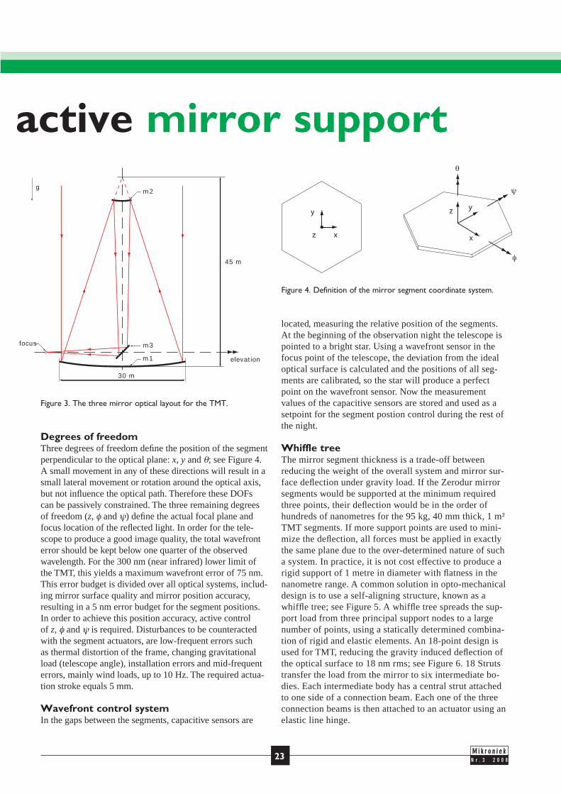
Degrees of freedomThree degrees of freedom defi ne the position of the segment perpendicular to the optical plane: x, y and θ; see Figure 4. A small movement in any of these directions will result in a small lateral movement or rotation around the optical axis, but not infl uence the optical path. Therefore these DOFs can be passively constrained. The three remaining degrees of freedom (z, φ and ψ) defi ne the actual focal plane and focus location of the refl ected light. In order for the tele-scope to produce a good image quality, the total wavefront error should be kept below one quarter of the observed wavelength. For the 300 nm (near infrared) lower limit of the TMT, this yields a maximum wavefront error of 75 nm. This error budget is divided over all optical systems, includ-ing mirror surface quality and mirror position accuracy, resulting in a 5 nm error budget for the segment positions. In order to achieve this position accuracy, active control of z, φ and ψ is required. Disturbances to be counteracted with the segment actuators, are low-frequent errors such as thermal distortion of the frame, changing gravitational load (telescope angle), installation errors and mid-frequent errors, mainly wind loads, up to 10 Hz. The required actua-tion stroke equals 5 mm.
Wavefront control systemIn the gaps between the segments, capacitive sensors are
located, measuring the relative position of the segments. At the beginning of the observation night the telescope is pointed to a bright star. Using a wavefront sensor in the focus point of the telescope, the deviation from the ideal optical surface is calculated and the positions of all seg-ments are calibrated, so the star will produce a perfect point on the wavefront sensor. Now the measurement values of the capacitive sensors are stored and used as a setpoint for the segment postion control during the rest of the night.
Whiffle treeThe mirror segment thickness is a trade-off between reducing the weight of the overall system and mirror sur-face defl ection under gravity load. If the Zerodur mirror segments would be supported at the minimum required three points, their defl ection would be in the order of hundreds of nanometres for the 95 kg, 40 mm thick, 1 m² TMT segments. If more support points are used to mini-mize the defl ection, all forces must be applied in exactly the same plane due to the over-determined nature of such a system. In practice, it is not cost effective to produce a rigid support of 1 metre in diameter with fl atness in the nanometre range. A common solution in opto-mechanical design is to use a self-aligning structure, known as a whiffl e tree; see Figure 5. A whiffl e tree spreads the sup-port load from three principal support nodes to a large number of points, using a statically determined combina-tion of rigid and elastic elements. An 18-point design is used for TMT, reducing the gravity induced defl ection of the optical surface to 18 nm rms; see Figure 6. 18 Struts transfer the load from the mirror to six intermediate bo-dies. Each intermediate body has a central strut attached to one side of a connection beam. Each one of the three connection beams is then attached to an actuator using an elastic line hinge.
30 m
45 m
g
elevationm1
m2
m3focus
x
y
z x
y z
θ
ψ
φ
Figure 4. Definition of the mirror segment coordinate system.
22_27_Flexure_nr3_2008.indd 2322_27_Flexure_nr3_2008.indd 23 06-06-2008 12:26:3506-06-2008 12:26:35

N r . 3 2 0 0 8 24
Figure 5. A schematic representation of a 2D whiffle tree.
Figure 6. The mirror segment is supported by the 18-point whiffle tree.
Lateral support structureThe lateral support structure must adequately support the mirror segment in x, y and θ, while leaving z, φ and ψ free to be actively controlled by the segment actuators. The tele-scope can tilt to up to 15° elevation (90° is pointing straight upwards) to enlarge the fi eld of view. The lateral support must therefore not only constrain the in-plane motion of the segments but also carry a fraction of their weight when the telescope is pointed to the horizon. An elastic parallel guide is added at every whiffl e tree-mirror interface point; see Figure 7. These parallel guides are oriented in tangential direction constraining the tangential motion of all interface points. They are however free to move in radial direction to allow for differences in thermal expansion between the frame and the mirror, with a thermal centre coinciding with the optical axis of the segment; see Figure 8. The axial di-rection is also free, allowing active control of z, φ and ψ. All these parallel guides are laser cut in the same 1 mm sheet of duplex stainless steel. The combined tangential stiffness of the parallel guides results in a fi rst mirror segment natural frequency of 145 Hz in x and y, and 195 Hz in θ. Due to the high in-plane stiff-ness of the mirror segment itself, the rms defl ection of the optical plane at 15° elevation is a factor two less (8.3 nm)
than at 90°. The force required to overcome the parasitic stiffness of the parallel guides when actuating the mirror segments, is delivered directly at the leaf spring by the actu-ators, without distorting the optical surface. The drive force also acts in the centre of the parallel guide, eliminating all reaction moments at the mirror interface. Using 18 parallel guides to constrain 3 DOFs results in a kinematically over-determined design. The initial stresses are minimized by mounting the mirror interface pads to the 18 parallel guides before gluing the mirror segment to all pads simultaneously.
Figure 7. Parallel elastic guide.
INSTRUMENTATION FOR LARGE OPTICAL TELESCOPES
mirror
intermediatebody
struts
g
principal support nodeconnection beam
axial freedom (actuator motion)radial freedom (thermal compensation)
radial direction
tangential direction
Figure 8. All parallel elastic guides are oriented in tangential direc-tion to provide a thermal centre coinciding with the optical axis.
22_27_Flexure_nr3_2008.indd 2422_27_Flexure_nr3_2008.indd 24 06-06-2008 12:26:3506-06-2008 12:26:35

N r . 3 2 0 0 825
A second sheet of stainless steel is used to provide a late-ral support for the intermediate bodies of the whiffl e tree. These so called ‘spiders’ are only constrained in z, φ and ψ by the struts of the whiffl e tree. Their in-plane motion is constrained in their center of gravity by three tangential struts, laser cut in the sheet for each spider; see Figure 9. Both sheets with lateral support fl exures are laser welded to a 50 mm thick spacer structure to form a stiff sandwich support plate, providing lateral support for the mirror and whiffl e tree components; see Figure 10.
Figure 9. Lateral support of the intermediate bodies by means of three tangential struts.
Figure 10. Lateral support plate assembly.
Active axial supportThree actuators are placed at the center of each whiffl e tree interconnection beam to control the segment z, φ and ψ, at 120°. The actuators are designed to be free of friction and play, like the lateral support structure and whiffl e tree, to guar-antee accurate performance over the lifetime of the telescope, specifi ed at 30 years. A mass-balanced voice coil is used, providing a friction-free, non-commutating actuator with low
power. Due to the balanced nature of the system, it is invari-ant to the elevation angle of the telescope and features low power consumption. This is extremely important, because heat dissipation behind the mirror segments would heat the mirror and result in a source of infrared radiation in the light path, destroying the capability to observe the universe at short wavelengths. The magnetic circuit of the voice coil is attached to a cantilever beam with a 1:4 ratio by a strut. The moving part of the actuator is designed to resemble 1/4 of 1/3 of the total mass of the mirror segment and whiffl e tree.
The 8.5 kg mass of the counterweight, mainly consisting of soft iron and NdFeB magnets, is guided by a double parallel elastic guide. The parallel guide allows for large displacements of ±10 mm. The coil assembly is attached to the actuator frame; see Figure 11. An optical encoder with a resolution of 5 nm is used for closed-loop position control of the actuator. The designed actuator has a maxi-mum force output of 500 N, with an actuator constant of 50 N/W½.
Figure 11. Cross section of the actuator assembly.
mirror bonding pad
whiffle tree intermediate body
280
344
cantilever beam
magnet assy
coil tube
connecting struts
frame interface
elastic hinge
paralel elastic guide
parallel elastic guide intermediate body
22_27_Flexure_nr3_2008.indd 2522_27_Flexure_nr3_2008.indd 25 06-06-2008 12:26:3606-06-2008 12:26:36

N r . 3 2 0 0 8 26
The Van Haendel cross spring hingeAn elastic hinge provides rotational freedom to the canti-lever and diverts the support load from the mirror to the frame. The hinge consists of a monolith wherein two re-inforced orthogonal leafsprings are produced using wire EDM. The centre of the reinforced section of leafspring A is separated to allow for leafspring B to pass through. Both sections of leafspring A are connected with bolts us-ing a thin plate on either side of the leafsprings. These two thin parallel plates (basically a parallel guide) introduce an internal degree of freedom in leafspring A, resulting in a kinematically defi ned (initially stress-free) and highly symmetrical elastic hinge. All accurate and elastic parts are produced using a single EDM production step, providing a compact and cost-effi cient elastic hinge: the Van Haendel cross spring hinge; see Figure 12.
Figure 12. The Van Haendel cross spring hinge.
System analysisIn order to attenuate disturbances up to 10 Hz, the stiffness of the entire active support must be high enough to place all relevant resonances above at least 50 Hz. Finite-element analysis of the fi nal design shows the fi rst resonance mode being φ and ψ at 68 Hz and z at 82 Hz. Above these fre-quencies the mirror mass decouples from the actuators.
Actuator testrigA prototype of the active support has been manufactured to provide data on the performance and experiment with different control parameters; see Figure 13. The mirror and whiffl e tree mass is replaced by a block of lead, attached to the cantilever beam by a strut with equal stiffness as the entire whiffl e tree; see Figure 14. A laser interferometer is used to measure the position of the load (lead block/mirror).
Figure 14. The assembled prototype actuator, the mirror mass being replaced by a lead block.
INSTRUMENTATION FOR LARGE OPTICAL TELESCOPES
A1 A2
B
connection plate
rotor
stator
mirror
lateral support
whiffle tree
actuator frame
telescope interface
Figure 13. Side view of the assembled active mirror support.
22_27_Flexure_nr3_2008.indd 2622_27_Flexure_nr3_2008.indd 26 06-06-2008 12:26:3806-06-2008 12:26:38

N r . 3 2 0 0 827
System identifi cation shows a fi rst resonance peak at 2.8 Hz; see Figure 15. This represents the total moving mass reso-nating on the combined parasitic stiffness of guides and the elastic hinge. At 59 Hz the mass decouples from the actua-tor. After tuning of the control parameters, the dynamic rms error on the actuator side equals 12.6 nm, with 5.1 nm on load side. With these results the project has been concluded successfully and the segment support has been offered to a number of ELT consortia.
AcknowledgmentThe design of the active mirror support would not have been possible without the support and involvement of Nick Rosielle from the Dynamics and Control Technology group, Eindhoven University of Technology, and Pieter Kappelhof (now at Mapper Lithography), Joep Pijnenburg, Arthur
Berkhoff, Robert Zuljar and Emile Noothout from TNO Science and Industry, Opto Mechanical Instrumentation group.
Author’s noteRob van Haendel is a mechatronics designer at Philips Applied Technologies in Eindhoven. Last year he won the Wim van der Hoek Award for the best Dutch graduation work in mechatronics.
-240
-220
-200
-180
-160
-140
-120
-100
-80
-60
-40
Mag
nitu
de (
dB)
10-1
100
101
102
103
104
-315
-270
-225
-180
-135
-90
-45
0
Pha
se (
deg)
SPECTRAL ESTIMATION
Frequency (Hz)
Figure 15. Measured frequency response of the prototype actuator.
www.dct.tue.nlwww.tno.nl
Information
22_27_Flexure_nr3_2008.indd 2722_27_Flexure_nr3_2008.indd 27 06-06-2008 12:26:4006-06-2008 12:26:40

N r . 3 2 0 0 8
TThere is a growing demand for high-precision coordinate measuring machines (CMMs). An important application involves 3D measurements of micro-products, such as Micro Electro Mechanical Systems (MEMS). Examples include watch cogs or the fluid ducts found in inkjet heads or injec-tion engines. High-precision probes have to be suitable for measuring these components. This is why these CMMs need a tactile sensor system with an uncertainty level substantially below 100 nm (Pril, 2002). Various Ph.D. students in Eindhoven and Delft have worked on the development of high-precision CMMs (Vermeulen, 1999; Ruijl, 2001; Van Seggelen, 2007) and a number of them are now available on the market. In 2003, a doctoral study was started at Eindhoven University of Technology entitled ‘Automatische assemblage van hybride microcomponenten’ (Automatic assembly of hybrid micro-components) (Bos, 2008). The study focused on the redesign of a 3D tactile sensor (Pril, 2002) with the aim of improving the assembly and the measuring accuracy. The new tactile sensor system was called Gannen XP.
How the system works The first prototype of the silicon chip, which forms the heart
of the Gannen XP tactile sensor system, is shown in Figure 1. The triangle in the middle of the chip can move relative to the outer edge using three small rods that are attached to the corners of the triangle. The deformation of the three rods is measured with piezo-resistive strain gauges attached to them.
Figure 1. Prototype of the silicon chip that forms the heart of the Gannen XP.
28
3D MEASUREMENT OF MICRO-COMPONENTS
Nanometre level uncertainty with
Coordinate measuring machines (CMMs) visualise a three-dimensional object by skimming
it with a spherical tip on a thin needle. To do so, a CMM uses a sensor system that directly
feeds back any contact between the tip and the object, enabling the machine to calculate
the displacement of the tip in three dimensions. By skimming a product in this way, either
by scanning or moving from point to point, the shape of the object can be reconstructed to
a high degree of accuracy. The uncertainty of the measurement is currently limited by the
accuracy of the available sensor systems. This article describes the redesign of a 3D measuring
probe aimed at improving its assembly process and measurement uncertainty.
• Edwin Bos •
28_32_Gannen_nr3_2008-1.indd 2828_32_Gannen_nr3_2008-1.indd 28 06-06-2008 12:27:0606-06-2008 12:27:06

the Gannen XP
N r . 3 2 0 0 8
Figure 2 shows one of the rods. The piezo-resistive strain gauges on the rod form a Wheatstone bridge, as shown in the diagram in Figure 3. When the probe tip is moved, two strain gauges are stretched (R
1 and R
2) and two strain gauges are
compressed (R3 and R
4). The Wheatstone bridge converts the
resulting change in resistance into an electrical signal Vm.
Figure 2. A rod in the prototype chip with four piezo-resistive strain gauges.
Figure 3. Diagram of how the probe works.
The probe tip is connected rigidly to the triangle in the mid-dle of the chip by the stylus. This inner triangle is suspended on the outer edge by three rods, which fixate three of its degrees of freedom. As mentioned before, the probe receives a mea surement signal from each rod. Using these three mea-surement signals, it is possible to calculate the remaining three degrees of freedom, thus determining the displacement of the probe tip.
High-precision measurements The measurement uncertainty of the Gannen XP (see Figure 4) is determined with the aid of a calibration set-up in which the displacement of a measurement mirror is measured simul-
taneously by the probe and a laser interferometer. This makes it possible to compare the displacement as measured by the probe to the same displacement as measured by the laser.
Figure 4. The Gannen XP on a high-precision coordinate measur-ing machine. (Photo: Bart van Overbeeke)
The deviation between the probe and the laser interferometer for a displacement in x, y and z direction is shown in Figure 5. For a period of 6 hours, the measurement mirror is moved back and forth 1,000 times over a distance of 5 micrometres in increments of 0.25 micrometres. The measured standard deviation between the probe and the laser interferometer is 2 nm at each measuring point for all directions. A second important value is the drift of the probe, which is shown in Figure 6 for a 60-hour measurement without con-tact with an object. This figure shows that the contribution made by the electronics and thermal tension in the design is less than 2 nm in any 20-minute interval.
29
28_32_Gannen_nr3_2008-1.indd 2928_32_Gannen_nr3_2008-1.indd 29 06-06-2008 12:27:0706-06-2008 12:27:07

N r . 3 2 0 0 8
Figure 5. Measurement deviation of Gannen XP in the x, y and z direction compared to a laser interferometer over a displacement of 5 micrometres.
Figure 6. Drift of the Gannen XP measured over a period of 60 hours in a temperature-conditioned room.
The combined 3D uncertainty at twice the standard devia-tion (k = 2) of the Gannen XP is 50 nanometres. The Gannen XP is one of the most accurate 3D measuring probes on the market today. The main limitations are the compensation for
unroundness and roughness of the probe tip. For the smaller tips in particular, with diameters of under 100 micrometres, it is still a major challenge to calibrate them and make them accurate enough. An important advantage of the Gannen XP is that the probe’s colliding mass and stiffness are extremely low, making it possible to avoid damaging products during the measur-ement. This damage influences the measurement and renders the often unique products unusable. This system can prevent these permanent deformations.
Measuring micro-components The increasing miniaturisation of components, such as the parts in mobile telephones, sensors in cars, computers and medical equipment, create a growing demand for methods to measure them. That is why the Gannen XM was introduced at the end of 2007, 18 months after the launch of the Gannen XP. The Gannen XM is specially designed for 3D measur-ements of these micro-components (see Figure 7). It can be used with probe tips with a diameter of 50 micrometres, half the thickness of a hair, so the probe fits into minute open-ings and holes. The low stiffness and replacement costs and the possibility of using extremely small probe tips make the Gannen XM ideal for measuring micro-components and MEMS.
Figure 7. The Gannen XM, the second tactile sensor system pro-duced by Xpress, was designed for 3D measurements of micro-products such as MEMS.
Influence of surface forces Measurements with tactile sensors are influenced by surface forces consisting of electrostatic, hydrostatic and Van der
30
3D MEASUREMENT OF MICRO-COMPONENTS
28_32_Gannen_nr3_2008-1.indd 3028_32_Gannen_nr3_2008-1.indd 30 06-06-2008 12:27:1006-06-2008 12:27:10

N r . 3 2 0 0 8
Waals forces. In order to measure with small tips without damaging the object, the contact forces between the probe tip and the object have to be reduced considerably. In the case of the Gannen XM, these forces are in the range of a few microNewtons. These contact forces, therefore, are in the same range as the surface forces between the probe tip and the object being measured. This makes its possible to measure these forces with the probe when the probe tip is close enough to the object. Figure 8 shows that the object attracts the probe tip before there is any contact between them. From a certain distance, the sur-face forces are high enough to pull the probe tip to the object. This is called the ‘snap-in’ effect.
Figure 8: The influence of surface forces during a measurement.
Partnership A number of companies worked on the research project and participated in the guiding committee, set up as part of the Innovation-driven Research Programme (IOP) for Precision Technology. As TNO Science and Industry’s technology partner, C2V (Concept to Volume) supplied the silicon chip in the tactile sensor system. The assembly was completed in close co-operation with TNO Science and Industry. Other important contributions to the project came from NTS Mechatronica, Mitutoyo, NMi, Delft University of Technology, Heidenhain, IBS Precision Engineering, Hogeschool Utrecht (Utrecht University of Applied Sciences) and the Joint Technical Department (GTD) of Eindhoven University of Technology.
31
In 2004, shortly after starting on his doctoral research, Edwin Bos set up Xpress Precision Engineering. The main aim of the firm was to support research and strengthen working relations with the industry. The improvements in the area of assembly resulted in a considerable reduction in the cost price of the probe. In combination with an improvement in measuring behaviour, this led to further steps toward the commercialisation of the tactile measuring system called Gannen XP. Ernst Treffers joined the company, which has been a private limited liability company since 2007. The Gannen XP is the first product to come from Xpress Precision Engineering. The name is based on the Japanese calen-dar, in which Gannen heralds a new era. ‘As far as we are con-cerned, our product not only symbolises the start of our compa-ny, but also an entirely new measuring era’, say Bos and Treffers.June 2007 saw the final of New Venture 2007, a Dutch competition for new businesses initiated by McKinsey & Company. The New Venture jury, which consisted of (pri-vate) investors, companies and coaches, was hugely enthusi-astic about the strategy and technological impact of Xpress. Of the 1,200 competitors, who submitted almost 500 busi-ness plans, Xpress was proclaimed the winner. A second major development in that year was when Xpress was awarded a first- and second-phase Valorisation Grant by Technology Foundation STW. A committee consisting of investors, entrepreneurs and scientists chose Xpress from a number of proposals on the basis of technical and commer-cial potential, the business team and their planning.
www.xpresspe.com
Edwin Bos (left) and Ernst Treffers after winning the final of New Venture 2007.
Xpress Precision Engineering
28_32_Gannen_nr3_2008-1.indd 3128_32_Gannen_nr3_2008-1.indd 31 06-06-2008 12:27:1206-06-2008 12:27:12

N r . 3 2 0 0 8
Author’s noteEdwin Bos was awarded his PhD on 8 April 2008 for the design of the Gannen XP at Eindhoven University of Technology (TU/e) and has been managing director of TU/e-spin-off Xpress Precision Engineering since 2004.
ReferencesE.J.C. Bos, Tactile 3D probing system for measuring MEMS with nanometre uncertainty, ISBN 978-90-386-1216-4, Ph.D. Thesis, Eindhoven University of Technology, 2008.W.O. Pril, Development of High Precision Mechanical Probes for Coordinate Measuring Machines, ISBN 90-386-2654-1, Ph.D. Thesis, Eindhoven University of Technology, 2002.T.A.M. Ruijl, Ultra Precision Coordinate Measuring Machine: Design, Calibration and Error Compensation, ISBN 90-6464-287-7, Ph.D. Thesis, Delft University of Technology, 2001.J.K. van Seggelen, NanoCMM: A 3D Coordinate Measuring Machine with low moving mass for measuring small products in array with nanometre uncertainty, ISBN 90-386-2629-0, Ph.D. Thesis, Eindhoven University of Technology, 2007.M.M.P.A. Vermeulen, High-Precision 3D-Coordinate Measuring Machine: Design and Prototype-Development, ISBN 90-386-2631-2, Ph.D. Thesis, Eindhoven University of Technology, 1999.
32
3D MEASUREMENT OF MICRO-COMPONENTS
28_32_Gannen_nr3_2008-1.indd 3228_32_Gannen_nr3_2008-1.indd 32 06-06-2008 12:27:1306-06-2008 12:27:13

N r . 3 2 0 0 833
CCollaboration is the order of the day in the Dutch high-tech systems industry. A number of large OEMs have joined forces in the High Tech Systems Platform. Together with system suppliers and knowledge institutes, they have initiated various major innovation programmes, such as the Programme for High Tech Systems and Point-One (for nano-electronics and embedded systems). The system suppliers have in turn merged or established alliances. And in late 2006, a group of ‘one-man shows’ joined forces in the High Tech Specialists Work Group and introduced themselves at the Precision Fair. The work group and the trade fair were both initiatives of Mikrocentrum.
The High Tech Specialists Work Group now comprises ten independent technological experts from various fields, from electrochemical machining and electrical discharge machining technology to high-precision design principles and the optimisation of production processes.
Clients can have projects carried out by one or more of the group’s specialists. The advantage of doing so is that they all know one another extremely well and can always resort to the know-how in the group. Joint marketing is a primary goal, since in a large group, the attention paid to marketing can be evenly spread over time. Furthermore, partners get to know and trust one another within the work group so they have no qualms about taking a partner to a client or
involving them in a project. The first projects worked on by members of the High Tech Specialists Work Group have already been completed.
MIKROCENTRUM : FROM PRECISION FAIR TO HIGH TECH SPECIALISTS WORK GROUP
Independent high-tech specialists join forces
Eindhoven-based Mikrocentrum is an independent compe-tence centre with a 40-year history of supporting companies and institutes. The main objectives are improving know-how and stimulating intercompany networking and co-operation. Mikrocentrum’s network extends into government(-related) organisations, as well as into scientific and educational insti-tutes, and its High Tech Platform comprises over 480 high-tech industrial companies. Annually, over 20,000 people participate in events organised by Mikrocentrum, such as 30 to 40 special-interest sessions on topics ranging from technology, product development and manufacturing to quality and management. Mikrocentrum also offers a comprehensive array of short, concise practi-cal courses and workshops in technology and management at all educational levels ranging from the hands-on technical up to the academic. Additionally, Mikrocentrum organises a dozen trade fairs a year in fields such as precision technology, industrial automation solutions, vision & robotics, and health & technology.
www.mikrocentrum.nl
Mikrocentrum
The well-known Precision Fair will be held for the 8th time on 26 and 27 November 2008 in Veldhoven (near Eindhoven). It is the lar-gest event in its field in the Netherlands. Over 2,500 visitors and 200 exhibitors are expected this year. The exhibition and the exten-sive lecture programme will devote special attention to vision, micro-systems, and piezo technology.
33_Microcentrum_nr3_2008.indd 3333_Microcentrum_nr3_2008.indd 33 06-06-2008 12:27:4006-06-2008 12:27:40

N r . 3 2 0 0 8
MMartin Hill (see Figure 1) performed his research at COBRA, the Eindhoven-based, Inter-University Research Institute on Communication Technology Basic Research and Applications. His laser has a diameter of 210 nm and its dimensions can be reduced considerably further, far below half a wavelength, which seems contradictory to laser fun-damentals. However, metallic sidewalls enable reduction of laser dimensions far below the wavelength. Before Hill’s publication in the leading journal Nature Photonics, many researchers were convinced that such metallic cavities would exhibit too high losses to achieve laser action, but Martin Hill’s perseverance showed that this conviction was wrong.
Figure 1. Martin Hill calculating the performance of his laser. (Photo: Bart van Overbeeke)
34
SMALLEST ELECTRICALLY PUMPED LASER EVER
Metal-coated
Dielectric micro-cavity semiconductor lasers used to have dimensions of many times the
wavelength of the emitted radiation. Now, Australian Martin Hill has succeeded in designing
and building a metallic nano-cavity laser with dimensions that are substantially smaller than
the wavelength of the emitted light. He has made a success of a job that experts considered
virtually impossible, thanks to his own tenacious determination and to the elaborate facilities
at Eindhoven University of Technology (TU/e). The new laser is still in the laboratory phase
of development and operates at liquid nitrogen temperature. TU/e researchers work hard to
make the laser function at room temperature. Hill’s achievement creates prospects for clock
frequencies in the Terahertz range (i.e. 1012 s-1) and incredibly small switching energies below
1 fJ (i.e. 10-15 J).
• Frans Zuurveen •
34_36_goldfinger_nr3_2008.indd 3434_36_goldfinger_nr3_2008.indd 34 06-06-2008 13:43:5106-06-2008 13:43:51

nano-cavity laser
N r . 3 2 0 0 8
Meint Smit, Eindhoven professor in opto-electronic devices, sees a great future for metallic nano-cavity lasers. Their tiny dimensions allow them to serve as the basis for high-speed digital processors, with up to a hundred thousand lasers in one opto-electronic circuit. Such opto-electronic ICs might be a factor of 100 faster than transistor ICs. They are less suited for memory circuits, however, because of their much higher static power consumption.
A submicron pillarThe basic geometry of this smallest laser in the world is shown in Figure 2. In reality, the laser consists of more layers than shown in the figure but for a better understanding, only three layers are represented. In a double hetero-structure, an active layer of a few hundred nanometres of InGaAs with an emission wavelength of about 1.65 µm is cladded between an n-type and a p-type doped InP layer. This structure is covered with a thin dielectric layer of 10-20 nm SiN. Finally, a layer of silver is deposited to form a lasing cavity.
Figure 2. Structure of the metal-coated semiconductor nano-cavity laser.
Figure 3 shows the laser structure as a pillar 200-300 nm in diameter and 1 µm in height observed with a scanning
electron microscope. In practice, the various layers are firstly deposited on a wafer after which the pillars are formed by e-beam litho graphy and ICP etching. After depositing SiN and metal, the dielectric layer is selectively opened to apply a metal contact layer.
Figure 3. SEM image of the pillar-like laser structure.
Part of the light in the cavity escapes through the bottom of the pillar and can be detected through the substrate, which is transparent for the emitted infrared light. In the future, slits in the metal wall will produce more efficient coupling of light out of the cavity. Figure 4 shows the simulated light distribu-tion of the lasing mode. The experimental set-up for testing the nano-cavity laser is represented in Figure 5.
Figure 4. Simulated light distribution of the lasing mode.
35
InP
Dielectric layer Metal
Active layerInGaAs Q1.65
34_36_goldfinger_nr3_2008.indd 3534_36_goldfinger_nr3_2008.indd 35 06-06-2008 13:43:5406-06-2008 13:43:54

N r . 3 2 0 0 8
Figure 5. Experimental testing set-up. (Photo: Bart van Overbeeke)
PlasmonicsFigure 6 shows some of Hill’s metal-coated nano-cavity lasers. Their small dimensions can be explained by the interaction of plasmons and photons. Plasmons are virtual particles that originate from the quantisation of oscillations in plasmas and metals. They play a part in the light reflection properties of metals. Light of frequencies below the plasma frequency is reflected, because the electrons in the metal shield the electric field from the light. Light of frequencies above the plasma frequency is transmitted because the elec-trons cannot respond fast enough to shield it. In most metals, the plasma frequency is in the ultraviolet range, making them reflective in the visible range.
Figure 6. Some of Hill’s metal-coated nano-cavity lasers. (Photo: Bart van Overbeeke)
Martin Hill made use of software that he modified for his purposes from a program he used when working in the Korean Advanced Institute for Science and Technology. With his adapted software, he could calculate and simulate resonance effects in his new laser. Figure 7 shows the light spectrum of his laser with a sharp peak at the 1400 nm wave-length. The inset shows spectra measured just below and above the threshold current of 6 µA.
Figure 7. Measured light spectrum of the laser with a sharp peak at the 1400 nm wavelength. Inset: spectra just below and above the threshold current of 6 µA.
Author’s noteFrans Zuurveen is a freelance text writer in Vlissingen, the Netherlands.
ReferencesM.T. Hill and M.K. Smit, Ultra-compact metal-coated semi-conductor nano-cavity lasers, EOS Conference, 2008.The smallest laser in the world (in Dutch: De kleinste laser ter wereld), Matrix (Eindhoven University of Technology), 14(4), 2007.Paul van Gerven, Goldfinger, the world’s smallest laser (in Dutch: Goldfinger, ’s werelds kleinste laser), Bits&Chips, April 2008.
36
SMALLEST ELECTRICALLY PUMPED LASER EVER
34_36_goldfinger_nr3_2008.indd 3634_36_goldfinger_nr3_2008.indd 36 06-06-2008 13:43:5606-06-2008 13:43:56

N r . 3 2 0 0 8
T
37
The new generation of extremely large reflecting tele-scopes is a recent phenomenon. The concept of construct-ing an optical telescope’s primary mirror from a number of mirror segments provided the breakthrough. The GTC on La Palma is a part of this new generation; see Figure 1. As a result of the pioneering optical sensitivity and resolution that this telescope will be able to realise, scientists can bet-ter study the underlying processes of the formation of stars, systems and the Universe. The most important research objective of the GTC will be obtaining and studying spec-tra in the NIR (Near-Infrared, 0.9-2.5 µm) wavelength region. For this purpose, the telescope will be equipped with an NIR multi-object spectrograph. To minimise back-ground noise, vacuum (10-6 mbar) and cryogenic (77 K) conditions are prevalent inside this instrument. Figure 1. Grand Telescopio de Canarias under construction.
ASTRONOMIC INSTRUMENTATION
Configurable Slit Unit for Canary telescope
On the Canary Island of La Palma, the world’s largest reflecting telescope is being built, the
‘Grand Telescopio de Canarias’ (GTC) with a diameter of 10.4 metres. Janssen Precision
Engineering is involved in the development of instrumentation for the GTC. For the past four
years, work has been done on the development of a specific and extremely compact drive and
measuring system for cryogenic and vacuum applications. This has finally led to the realisation
of a demonstration model of the Configurable Slit Unit for the GTC infrared instrument.
This is an updated version of the article that was previously published (in Dutch) in
Mikroniek 2006, no. 2.
• Norbert Meijs and Maurice Teuwen •
37_42_CSU+UVA_nr3_2008.indd 3737_42_CSU+UVA_nr3_2008.indd 37 06-06-2008 12:28:4606-06-2008 12:28:46

N r . 3 2 0 0 8
Configurable Slit UnitOne of the most complex parts of the spectrograph is the Configurable Slit Unit (CSU). This is a configurable mask, which is positioned at the spectrograph’s entrance focal plane (340 x 340 mm). The mask consists of 110 bars that can be positioned arbitrarily within the instrument’s image field (see Figure 2). The space that remains between two bars placed opposite each other is called a slit. The slits are used as a mask during spectrographic recording. Because a number of slits can be distributed across the image field, it is known as a multi-object spectrograph. In this way, a number of stars can be viewed simultaneously. The con-figuration of the slits will be changed several times a night.
Figure 2. Draft layout of the CSU (in a previous 100-bar version).
The following specifications roughly apply to the mask.
Number of bars: 110 (2 x 55)Stroke per bar: 340 mmBar position accuracy: < 10 µmBar speed: > 1 mm / sPitch bar - bar: 340 mm / 55 ~~ 6 mmEnvironmental conditions: 10-6 mbar, 77 K (-196 °C)
Janssen Precision Engineering (JPE), situated near Maastricht Airport, the Netherlands, became involved in the development of the CSU at the end of 2003. Challenged by the extreme specifications, it developed a concept for the accurate positioning of the bars under cryogenic and vacuum conditions on its own initiative. The concept was developed into a prototype, which formed the basis for further collaboration with the ‘Instituto de Astrofísica de Canarias’.
‘Inertial piezo drive’ conceptThe given preconditions with regard to the environmental conditions drastically limit the options for a suitable actua-tor principle. In addition, there is limited available enve-lope in which to build, imposed by the 6 mm pitch between
two successive bars. Furthermore, there is the requirement that the actuator must dissipate absolutely no energy when at a standstill; each heat source within the cryostat could create an aberration in the extremely sensitive infrared detector. Finally, the cost price is obviously also an impor-tant factor considering a total of 110 individual actuators are necessary.It was decided to use a piezo as the fundamental building block in realising the actuator. Piezos are extremely suit-able in this application because of a combination of proper-ties: vacuum compatibility, minimal outgassing; cryogenic-compatibility and extremely low dissipation.
To limit the number of piezo actuators, a concept was con-sciously sought with only one piezo for every moving bar. For this, the so-called ‘inertial drive’ concept was used. Figure 3 shows the actuator concept. The piezo is included in a mechanism that pushes against the bar with pre
-
tension force F. Together with two guiding wheels, this mechanism also forms the guide for the bar. By gradually increasing the voltage on the piezo, it will slowly extend. The accelerating power that occurs can be transferred by friction contact onto the bar, which will move in equal proportion. Should the piezo be abruptly discharged, the occurring acceleration will be so large that the accompany-ing acceleration power cannot be transferred from actuator to bar; through inertia, the bar remains virtually still while the actuator is dragged back over the full stroke. By repeat-ing this cycle, a net-movement can be realised.
Figure 3. ‘Inertial piezo drive’ actuator concept.
38
ASTRONOMIC INSTRUMENTATION
37_42_CSU+UVA_nr3_2008.indd 3837_42_CSU+UVA_nr3_2008.indd 38 06-06-2008 12:28:4706-06-2008 12:28:47

N r . 3 2 0 0 8
From an electrical point of view, this cycle can be viewed in the following way. In the electrical respect, the piezo acts as a capacity. The speed of charging and discharging is proportional to the RC time of the equivalent network in which the piezo is included. Based on the electrical diagram in Figure 4, an amplifier has been realised for controlling the piezo. The design of the actuator is charac-terised by the following properties:• simple, elementary; this is particularly important bear-
ing in mind costs and lifespan;• play-free design; this is particularly important for the
transition from room temperature (assembly) to cryo-genic temperature (operation), a large temperature transition that requires a design that can handle ex pansion differences;
• by definition, dissipation-free when standing still.
Figure 4. Electrical diagram of the piezo control.
Capacitive position measuring systemPosition measuring per bar is necessary in order to realise an accurate positioning of the bars. The choice of this measur-ing system was, once again, limited by environmental pre-conditions, limited envelope to build within and cost price.A capacitive measuring principle was chosen. Decisive fea-tures for choosing this measuring principle are:• the quantity (capacity) to be measured is not influenced
by the environmental conditions (vacuum, cryogenic temperature);
• the actual sensor consists of no more than two conduc-tors facing each other, so that:– the sensor can easily be made vacuum-compatible; – there is a relatively high degree of freedom in the
sensor’s design by finishing the required conductor plates as a vacuum vaporised conductor on a cera-mic base plate.
The accepted method for measuring movement with the aid of a capacitive measuring system is the measuring of the capacity between two conducting surfaces. With this, the measured capacity is inversely proportional to the variable distance between the conducting surfaces. The accompany-ing range, however, is typically ≤ 1 mm and therefore not suitable for the measuring of movements up to 340 mmTherefore, an alternative application of this measuring prin-ciple has been developed. The two conducting surfaces are placed a set distance apart from each other. By moving a conductor between the two conducting surfaces, the meas-ured capacity will increase. This principle is illustrated in Figure 5. The measured variation in capacity is now, on the one hand, dependent on the movement x and on the other it is limited by the ratio between distance D and distance D-d. Note that a transverse movement of the conductor between the plates (⊥ x) has no influence on the measured capacity!
Figure 5. Capacitive movement measuring system.
39
CHARGING
volta
ge
time
DISCHARGING
37_42_CSU+UVA_nr3_2008.indd 3937_42_CSU+UVA_nr3_2008.indd 39 06-06-2008 12:28:4806-06-2008 12:28:48
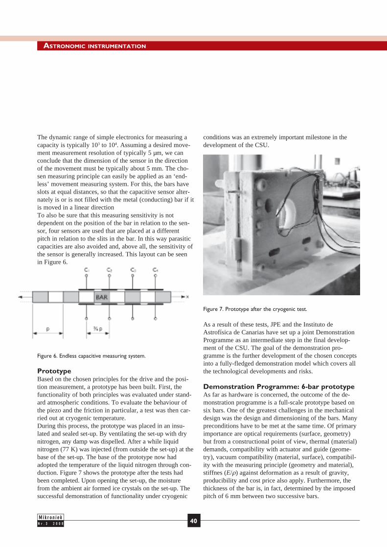
N r . 3 2 0 0 8
The dynamic range of simple electronics for measuring a capacity is typically 103 to 104. Assuming a desired move-ment measurement resolution of typically 5 µm, we can conclude that the dimension of the sensor in the direction of the movement must be typically about 5 mm. The cho-sen measuring principle can easily be applied as an ‘end-less’ movement measuring system. For this, the bars have slots at equal distances, so that the capacitive sensor alter-nately is or is not filled with the metal (conducting) bar if it is moved in a linear directionTo also be sure that this measuring sensitivity is not dependent on the position of the bar in relation to the sen-sor, four sensors are used that are placed at a different pitch in relation to the slits in the bar. In this way parasitic capacities are also avoided and, above all, the sensitivity of the sensor is generally increased. This layout can be seen in Figure 6.
Figure 6. Endless capacitive measuring system.
PrototypeBased on the chosen principles for the drive and the posi-tion measurement, a prototype has been built. First, the functionality of both principles was evaluated under stand-ard atmospheric conditions. To evaluate the behaviour of the piezo and the friction in particular, a test was then car-ried out at cryogenic temperature.During this process, the prototype was placed in an insu-lated and sealed set-up. By ventilating the set-up with dry nitrogen, any damp was dispelled. After a while liquid nitrogen (77 K) was injected (from outside the set-up) at the base of the set-up. The base of the prototype now had adopted the temperature of the liquid nitrogen through con-duction. Figure 7 shows the prototype after the tests had been completed. Upon opening the set-up, the moisture from the ambient air formed ice crystals on the set-up. The successful demonstration of functionality under cryogenic
conditions was an extremely important milestone in the development of the CSU.
Figure 7. Prototype after the cryogenic test.
As a result of these tests, JPE and the Instituto de Astrofísica de Canarias have set up a joint Demonstration Programme as an intermediate step in the final develop-ment of the CSU. The goal of the demonstration pro-gramme is the further development of the chosen concepts into a fully-fledged demonstration model which covers all the technological developments and risks.
Demonstration Programme: 6-bar prototypeAs far as hardware is concerned, the outcome of the de -monstration programme is a full-scale prototype based on six bars. One of the greatest challenges in the mechanical design was the design and dimensioning of the bars. Many preconditions have to be met at the same time. Of primary importance are optical requirements (surface, geometry) but from a constructional point of view, thermal (material) demands, compatibility with actuator and guide (geome-try), vacuum compatibility (material, surface), compatibil-ity with the measuring principle (geometry and material), stiffnes (E/ρ) against deformation as a result of gravity, producibility and cost price also apply. Furthermore, the thickness of the bar is, in fact, determined by the imposed pitch of 6 mm between two successive bars.
40
ASTRONOMIC INSTRUMENTATION
37_42_CSU+UVA_nr3_2008.indd 4037_42_CSU+UVA_nr3_2008.indd 40 06-06-2008 12:28:5006-06-2008 12:28:50

N r . 3 2 0 0 8
Figure 8 shows the final design of the bars. On the left side of the figure, a cross-sectional profile of the bars can be seen; in the final application, light (in this view) will enter from the right side of the instrument. In order to block the light as well as possible, the bars overlap in a labyrinthine construction. On the right of the figure, it can be clearly seen that the bar has slots required for the measuring system.
Figure 8. Design of the bars.
Ceramic sensorThe sensor is made of ceramic material. Metallic surfaces, applied by CVD, form the active sensor probes. The meas-urement signal is read out by a specifically designed meas-uring system that uses the ‘active guarding’ technique. This means that the capacitive measuring signal is actively fed back to the shielding of the vacuum-compatible, coaxial measuring cable. In this way, the capacity between core and shielding is eliminated from the measurement and the sensitivity to environmental disturbances is also limited. The four capacities are sequentially read out using a mul-tiplexer. Then an AD converter digitalises the measuring signals. Figure 9 shows the sensor.
The actuator mechanism is realised as a monolithic design in aluminium; see Figure 10. The two guides inside the mecha-nism are realised by means of elastic hinges. The piezo is mechanically pre-tensioned within the mechanism using a wire spring. A second wire spring realises the pre-tension of the actuator in the direction of the bar. For the positioning
of the bar, feedback from the measuring system is necessary. Control of the piezo and measuring of the position are carried out by a 32-bit micro-controller. The signals from the four capacities, read out by the AD-converter, must be combined into a linear measuring signal. For this purpose, an interpola-tion algorithm has been designed that determines positions within the periodic slot pattern in the bar. This algorithm is based on a look-up table, obtained through calibration of the bar. The micro-controller is further equipped with an interface for a higher control level. Homing and positioning commands can be introduced at this level, which is equipped with a graphic user interface. See Figure 11 for the measuring system.
FutureThe successful delivery of the 6-bar CSU prototype by Janssen Precision Engineering to the Instituto de Astrofísica de Canarias does not mark the actual end of the development. In the meantime, the public tender procedure for the develop-ment of the definitive instrument has been completed and the contract awarded to JPE. The development of the definitive instrument with 110 bars (see Figure 12) will be realised based on the tested concepts. Delivery is planned for the beginning of 2009. In the project, JPE is ultimately respon-
41
Figure 10. The actuator mechanism.
Figure 11. The measuring system for reading-out and digitalising the measuring signal.
Figure 9. The capacitive sensor.
37_42_CSU+UVA_nr3_2008.indd 4137_42_CSU+UVA_nr3_2008.indd 41 06-06-2008 12:28:5006-06-2008 12:28:50

N r . 3 2 0 0 8
sible for the total realisation of the instrument. The project will be carried out in co-operation with the sub-contractor NTE (Barcelona, Spain). NTE is responsible for the work-ing out and realisation of the necessary electronics.
The acquired experience in the development of instruments for use in cryogenic applications is, for Janssen Precision Engineering, supplementary to the existing expertise in the development of vacuum applications and precision mechatronic systems.
Authors’ noteNorbert Meijs is a freelance text writer in Cadier & Keer, the Netherlands, and Maurice Teuwen is project manager CSU at Janssen Precision Engineering, Maastricht, the Netherlands.
42
ASTRONOMIC INSTRUMENTATION
Janssen Precision EngineeringHuub Janssen, directorTel. +31 (0)43 - 358 57 77www.jpe.nl
Information
MAKE LIGHT | MANAGE LIGHT | MEASURE LIGHT AD-050807-EN
For more than 35 years the Newport name has been synonymouswith precision positioning system solutions and has built thousandsof precision motion systems for hundreds of applications in thearea of semiconductor wafer inspection, sensor test and calibration,laser machining, metrology, and ultra-precision assembly.
Newport offers many customizable products and solutions. X marksjust the beginning:
• XPS controller - High-performance, easy to use, integratedmotion controller/driver, high-speed communication.
• XM stages - Ultra-precision motion, high dynamics, reliabilityfor 24/7 production environments.
• X-factor - Wide breadth of standard solutions, customizableproducts, experience
Our extensive experience and custom solutions will answer themost challenging motion requirements - from A to Z. Call us todayor visit www.newport.com/Xfactor8
X Marks the Spot for
High Performance Motion
BelgiumNewport Spectra-Physics B.V.
Phone: +32 (0)0800-11 257Fax: +32 (0)0800-11 302
NetherlandsNewport Spectra-Physics B.V.Phone: +31 (0)30 659 21 11
Fax: +31 (0)30 659 21 [email protected] © 2008 Newport Corporation.
Figure 12. Design of a Configurable Slit Unit.
37_42_CSU+UVA_nr3_2008.indd 4237_42_CSU+UVA_nr3_2008.indd 42 06-06-2008 12:28:5106-06-2008 12:28:51
N r . 3 2 0 0 843
T
MEASUREMENT IN THE WORKSHOP AND IN SERIES PRODUCTION
The touch probes are available in two versions, depending on the application:
The TS workpiece touch probe is inserted directly into the • machine tool spindle. It can be ordered with a cable or with an infrared interface. Some of its typical tasks are work-piece alignment, presetting, and workpiece measurement.The TT tool touch probe permits fully automatic measu-• rement of stationary or rotating tools right in the machine, depending on the functions featured by the NC control.
High long-term stabilityWhen the probe contact is defl ected, HEIDENHAIN touch probes generate a trigger signal from an optical sensor. A
lens system collimates the light generated from an LED and focuses it onto a differential photocell. When the stylus is defl ected, the point of light changes its position on the pho-tocell, releasing a trigger signal. With the contact-free ope-ration of the optical switch, the sensor does not wear, which guarantees the high long-term stability of HEIDENHAIN touch probes.
Optical displayWith the HEIDENHAIN touch probes’ optical display, the user can check whether the touch probe is properly swit-ched off or on. The device indicates its readiness explicitly with a blinking light. Manual probing is also very conve-
• DR. JOHANNES HEIDENHAIN GmbH •
The use of touch probes reduces setup times,
helps to increase machine usage time, and
improves the dimensional accuracy of the
finished workpieces. Their setup, measuring
and monitoring functions can be performed
manually or automatically. Touch probes
are used primarily on milling machines and
machining centers, and they are suitable for
a large number of measuring tasks – both in
the workshop and in series production.
Workpiece touch probes
increase productivityin manufacturing
43_45_heidenhain_nr3_2008.indd 4343_45_heidenhain_nr3_2008.indd 43 06-06-2008 12:29:1606-06-2008 12:29:16

N r . 3 2 0 0 8 44
MEASUREMENT IN THE WORKSHOP AND IN SERIES PRODUCTION
nient for the user because stylus defl ection is indicated by a continuous light.
Operating times more than doubledWorking with the standard touch probes TS 640 and TS 440 has become more convenient. The revised electronics now operate signifi cantly more economically, so that the opera-ting time with one set of batteries has more than doubled. The operating time, i.e. the time for which the touch probe is actually in operation, is now approx. 800 hours for the TS 640 and approx. 200 hours for the compact TS 440.This example illustrates the improvements:Assuming that probing occupies 5% of working time and a plant runs three shifts for 220 days per year, the batteries would not need to be exchanged until after about three years for the TS 640 and after about three quarter of a year for the TS 440.
Different possible types of batteriesHEIDENHAIN touch probes are supplied with lithium bat-teries. This makes it possible to keep the intervals between battery exchange as long as possible. Besides lithium batte-ries, HEIDENHAIN touch probes can also be operated with standard alkaline batteries or rechargeable batteries. Thank to the sophisticated electronics, even batteries with very low voltage can be used. With these batteries, however, you would have to plan for shorter battery exchange intervals.
TS 740 - The Infrared Touch Probe System for Stringent RequirementsStandard touch probes like the TS 640 and TS 440 operate on the principle of an optical switch as sensor. The TS 740, however, which was introduced at the EMO 2007, features a newly developed sensor with pressure elements at its core. When probing a workpiece, the stylus is defl ected so that a force acts on these elements. The difference in forces is calculated by the electronics, and the trigger signal is gene-rated. This system makes a probing accuracy of ≤± 1 µm and a probing repeatability of 2 σ ≤ 0.25 µm possible.
The TS 740 is designed for use in modern machine tools with fast tool changers. Likewise, rapid acceleration or de-celeration does not cause uncontrolled trigger signals. The TS 740 distinguishes itself from the TS 640 with its higher probing accuracy and repeatability at a probing speed of 0.25 m/min (TS 640: 3 m/min), and by its lower probing forces. The more complex electronics, however, necessitate
shorter operating times between battery exchange than for the standard touch probes.The new TS 740 infrared touch probe is used to perform measurement tasks in a machine tool where there is an especially high demand regarding the accuracy and repeat-ability of the touch probe.
TS 444 - Battery-Free, Air-Driven Touch ProbeThe TS 444 offers an innovative and smart solution: at the same time that it cleans the probing point, it generates its own energy. Compressed air must be supplied through the spindle in order to use the TS 444. The air is introduced into the touch probe via the taper shank and powers a turbine wheel inside the touch probe. The turbine wheel generates electrical energy through changes in the magnetic fi eld, which is stored in high-power capacitors. As with conventi-onal touch probes, the exit air is used for cleaning the pro-bing point. This means that at the same time that the touch probe is charged with energy, the probing point is cleaned. Those who use the TS 444 need not handle, store or dispose of any batteries.
The charging time varies depending on the pressure: the higher the pressure, the shorter is the charging time. A supply pressure of 5 bars or more is recommended to ensure that charging is complete in a reasonably short time. For example, when a pressure of 5.5 bars is used, the touch probe is fully charged after around 3 seconds. With fully charged capaci-tors, the touch probe is able to probe for two minutes.
This touch probe is particularly interesting for those who manufacture in series and cannot allow any interruption in their processes at critical times in order to exchange batte-
Figure 1. The TS 740 at work.
43_45_heidenhain_nr3_2008.indd 4443_45_heidenhain_nr3_2008.indd 44 06-06-2008 12:29:1706-06-2008 12:29:17

N r . 3 2 0 0 845
ries. But the TS 444 is also an interesting alternative for users who very seldom use a touch probe but cannot afford the delay that occurs when the proper size of batteries is not immediately available.
Tool MeasurementTool measurement on the machine shortens non-productive times, increases machining accuracy and reduces scrapping and reworking of machined parts. With the contactless scan-ning of the TT 3-D touch probes and the contact-free TL laser systems, HEIDENHAIN offers two completely diffe-rent possibilities for tool measurement:
TT 140• The trigger signal is generated through a wear-free optical switch that ensures high reliability. The disk-type probe contact is easy to exchange. The connection pin to the touch probe’s contact plate features a rated break point. This protects the touch probe very effectively from physi-cal damage due to operator error.TL laser systems• The TL Micro and TL Nano laser systems can measure tools at the rated speed without making contact. With the aid of the included measuring cycles you can have tool
lengths and diameters measured, the form of the indivi-dual teeth inspected, and the tool checked for wear or breakage.
ConclusionHEIDENHAIN touch probes offer a number of new benefi ts and innovations. Among these are their extremely extended operating times and more fl exible battery handling with the standard models. In addition, the fl ushing/blowing feature typical to HEIDENHAIN touch probes now serves to power a new touch probe that operates entirely without batteries. Besides the optical standard sensor, HEIDENHAIN has introduced to the market a new sensor principle for very high measuring accuracy and, with it, offers one of the most accurate touch probes now available for machine tools on today’s market.
Figure 2. TS 444 principle of function.Figure 3. Tool measurement options:(a) TT.(b) TL.
www.heidenhain.com
Information
a
b
43_45_heidenhain_nr3_2008.indd 4543_45_heidenhain_nr3_2008.indd 45 06-06-2008 12:29:1806-06-2008 12:29:18

N r . 3 2 0 0 8
L system offers a solution. The passive system then ensures isolation of high-frequency disturbances and the active system ensures the correct static position of the machinery and sufficient damping of the low-frequency suspension modes. A machine frame has many more vibration modes, which mainly describe internal deformations of the frame at higher frequencies. To minimise their negative influence on accuracy, the frame must, to begin with, be as stiff as possible and have a mass as small as possible (the prin-ciples of ‘stiffness management’ and ‘weight watching’). However, stiffness cannot be increased limitlessly. The designer also has to take into account other design princi-ples such as ‘kinematic design’ [4].
46
DESIGN PRINCIPLES FOR PRECISION MACHINERY
For the development of precision machinery, a limited number of well-known design
principles apply. They include stiffness management, ‘weight watching’, kinematic
design, and elimination of friction and backlash. A disadvantage of constructions
designed in this way is a lack of damping. The Smart Disc concept uses piezoelectric
sensors and actuators to actively dampen vibrations. The challenge in designing accu-
rate, well-dampened machine frames lies in having the control technology – in itself
not overly complicated – accepted as an established design principle.
This article is a compilation of two articles that were previously published (in Dutch)
in Mikroniek, 2002, no. 5 and 2005, no. 4.
• Jan Holterman and Theo J.A. de Vries •
Large spacecrafts must be extremely light, and consequent-ly, usually are very flexible and easily induced to vibrate. Damping the vibrations is no simple task. Traditional, passive solutions such as applying visco-elastic materials to large surfaces quickly add too much weight to the equa-tion. In space travel, therefore, it seemed obvious to switch to active damping with sensors that can measure the vibra-tions and actuators that can reduce them.
In precision machinery, active vibration control in the form of vibration isolation is not new either. Most disturbances enter through the floor, which is a reason to place the machinery on special vibration isolators. If necessary, the combination of a passive system and an actively controlled
Active damping using Smart Discs
46_56_actieve demping_nr3_2008.indd 4646_56_actieve demping_nr3_2008.indd 46 06-06-2008 12:29:4706-06-2008 12:29:47

N r . 3 2 0 0 8
Wafer scanner lens suspensionTake the suspension of a wafer scanner lens (see the box). In Figure 1, the so-called main plate represents the ‘clean world’. It stands on three air mounts (active pneumatic vibration isolators) and is almost unaffected by vibrations from the floor. The lens is suspended in a circular hole made in the main plate. This lens is, in fact, a stack of lens-es with a total height of about 1 m and a diameter of 0.5 m. The lens is set in a flange that, in turn, is mounted to the main plate with the aid of three identical steel blocks, the so-called lens supports.
Figure 1. Diagram of the lens suspension in a wafer scanner.
In order to define all six degrees of freedom of the lens exactly once (the principle of ‘kinematic design’), each of the lens supports must define two coordinates, vertical and tangential (y and z in Figure 2). Locally, the remaining four coordinates must be left free and, for that, a lens support must be fitted with various hinges. In order to avoid back-lash and friction, notorious sources of inaccuracy, the use of elastic hinges is an obvious choice [4].
A conventional lens support is fitted with two horizontal elastic hinges across the entire length (see Figure 2). This means, however, that for each suspension point only two coordinates (x en ϕx) are left free, whereas it should have been four coordinates. This is the result of a trade-off between the principles of ‘stiffness management’ and ‘kinematic design’: a lens support with more than two elastic hinges would result in too much stiffness loss.
A consequence is that the two end surfaces of a lens sup-port, and with these the corresponding reference surfaces in the machine, must be presented sufficiently parallel.
47
piezoelectric
Wafer scanners are used in the production of ICs (integrated circuits). Through a lithographic process, they apply a pat-tern of electronic circuits onto a silicon wafer. The reticle with the desired pattern is positioned by a stage at the top of the machine. The wafer is positioned by the wafer stage. Between both stages, there are various stacked lenses (in short, lens). This lens projects the desired pattern onto the silicon. The non-exposed material on the wafer is etched away, so that a circuit with the desired form remains. The smaller the pattern, the more circuits per wafer and the faster the chips.The wafer scanner is an excellent example of a precision machine; the specifications are formulated in terms of nano-metres. The lens suspension of a wafer scanner frame that was specially adapted for this purpose served as the test assembly for the Smart Disc experiments described here.
Figure A. Simple representation of the lithographic process in a wafer scanner.
Wafer scanner
46_56_actieve demping_nr3_2008.indd 4746_56_actieve demping_nr3_2008.indd 47 06-06-2008 12:29:4806-06-2008 12:29:48

N r . 3 2 0 0 8
Figure 2. Diagram of a conventional lens support.
For the analysis of the system (main plate and lens, to gether properly isolated from the floor) we assume, for the sake of convenience, that no internal deformation occurs. The dynamic behaviour can then be characterised by six vibration modes of the lens with respect to the main plate (Figure 3):• Two joystick modes, with the lowest natural frequen-
cies (approx. 100 Hz). In these modes, the lens tilts around an axis in the suspension plane (x-y-surface in Figure 1). These modes are due to the limited vertical stiffness of the lens supports.
• Two pendulum modes. The lens moves more or less horizontally in the suspension plane. These modes are particularly due to the limited horizontal stiffness, i.e. the shear stiffness of the lens supports.
• In the two remaining vibration modes (not shown in Figure 3), there is relative vertical displacement and relative rotation around the vertical axis, respectively.
In the wafer scanner, the joystick modes and, to a lesser extent, the pendulum modes result in the highest vibration levels.
Figure 3. Diagram of the dominant vibration modes of the lens with respect to the main plate.
Reference experimentThis article firstly focuses on active damping of both joy-stick modes. To make a joystick mode clearly visible, a ref-erence experiment was carried out [6]. For this experiment, it was attempted to measure the joystick rotation around the (randomly chosen) x-axis in Figure 1, or rotation in the drawing surface in Figure 4. The air mounts were used to introduce a controllable disturbance to the main plate, the torque Tam around the x-axis. This torque is a white noise signal (0-300 Hz). The spectrum of the disturbance is there-fore flat in a sufficiently broad frequency range.
Figure 4. Side view of the test set-up for determining the joystick rotation around the x-axis.
The joystick rotation ϕx(t) cannot be measured directly. Instead, the rotation is reconstructed from four acceleration measurements, on the lens and the main plate (the white squares in Figure 4), with the aid of the following equation:
abottom(t) – atop(t) amp,2(t) – amp,1(t)ϕx(t) = ∫∫ [ –––––––––––––– – –––––––––––––– ] (dt)2 hlens wmp
The results of the reference experiment are shown in Figure 5 (also see the box).
48
DESIGN PRINCIPLES FOR PRECISION MACHINERY
46_56_actieve demping_nr3_2008.indd 4846_56_actieve demping_nr3_2008.indd 48 06-06-2008 12:29:4906-06-2008 12:29:49

N r . 3 2 0 0 8
Figure 5. Results of the reference experiment.Top: the reconstructed joystick rotation.Middle: the accompanying Power Spectral Density PSD.Bottom: the accompanying cumulative PSD.
This reference experiment shows an amplitude of the joy-stick rotation of 0.43 μrad. Furthermore, it appears from
the steep step around 110 Hz in the cumulative PSD that this rotation emanates almost completely from the lack of damping of the joystick modes. Further inspection of the measuring results has revealed that the damping ratio of the joystick modes amounted to only 0.2% [6].In theory, this low value of the damping does not have to be a problem but in practice it is impossible to isolate the lens and the main plate completely from all disturb-ing forces in the vicinity. The acoustics turn out to be the most important source of disturbance; the air in the system moves around a lot.
The obvious solution is to increase the damping in the sys-tem. Passive damping in mechanical systems, however, is mainly caused by friction and this is mostly disastrous for accuracy. Just as in space travel, the step to active damp-ing is a logical one. The main challenge with this is to guarantee the stability of the controlled system. The control design is based on a model, i.e. a simplification of reality. Non-modelled vibration modes can easily cause instability. The simplest way to prevent this is to use the collocated control principle: the closing of a control loop between a sensor and an actuator that are positioned at the same place in the system [5].
49
and with this the 3σ value can then be determined. The following is derived from Figure 5:
3σ = 3 2.1•10-14 = 0.43 μrad1/2
The cumulative PSD in Figure 5 shows that this power is almost totally attributable to one of the joystick modes (at 110 Hz). From the PSD, however, it becomes clear that the accel-eration sensors also pick up small contributions from other vibration modes:• the other joystick mode (at 105 Hz; from this it becomes
clear that, in practice, the assembly is not completely sym-metrical);
• a mode around 140 Hz (torsion from the main plate; so, the main plate does deform, contrary to one of the assumptions made for the purpose of simplification in this article);
• modes around 280 Hz (the so-called pendulum modes, by which the lens moves more or less horizontally in the plane of suspension; see Figure 3).
Two important characteristics of a signal x(t) are the mean μ and the standard deviation σ. The power P of a signal is equal to the sum of μ squared and σ squared. A suitable measure for the amplitude of a noisy signal is the 3σ value. A normally distribut-ed signal is within the limits [μ–3σ, μ+3σ] for 99.7% of the time.For the contribution of certain vibration modes to the ampli-tude of the measured signal, the frequency content of the signal is important. The Power Spectral Density, PSD(f), is a measure of the power at frequency f. The cumulative PSD is defined as the surface under the PSD up to frequency f:
cumPSD(f) = Σ f0 PSD(ρ)dρ
The end value of cumPSD is equal to the total signal power. When μ is equal to zero, the standard deviation can be calcu-lated from the end value of cumPSD:
σ = cumPSD(fmax)
Power Spectral Density
46_56_actieve demping_nr3_2008.indd 4946_56_actieve demping_nr3_2008.indd 49 06-06-2008 12:29:5006-06-2008 12:29:50

N r . 3 2 0 0 8
Smart Disc conceptThe so-called Smart Disc concept [1] enables collocated control. The Smart Disc is an active structural element for improving the dynamic behaviour of precision machinery and can be realised with the aid of piezoelectric material. This material can serve as an actuator (it expands under the influence of a voltage) but also as a sensor (when it is sub-jected to a force, an electric charge is the result).
Within the framework of the Smart Disc research project [1], two prototype active lens supports fitted with a piezo-electric position actuator and a piezoelectric force sensor were developed for the wafer scanner. The first prototype, the Smart Lens Support (SLS), was aimed at active damp-ing of the joystick modes. In order to enable active damp-ing of these modes by means of three identical SLSs, each SLS should locally display Smart Disc functionality in the vertical direction, i.e. have the ability to measure a local vertical force and produce a local vertical displacement.
SLS - mechanical designThe mechanical design of the Smart Lens Support [7] is based on the conventional lens support and has the same dimensions (100 x 20 x 60 mm3). The two horizontal elastic hinges are copied, just as the foundation surfaces and the threaded holes for the bolts on the top and bottom sides. The SLS is constructed from (see Figure 6):• a flexure block;• two actuator-sensor stacks, each consisting of an
actuator (multi-layer, to be able to realise a reasonable
expansion, even with a limited voltage) and a single-layer sensor;
• a preload bolt with two accompanying nuts.
Symmetry in the design should ensure purely vertical dis-placement when the actuators are controlled. In addition, the design contains an elastic preload element, which is necessary because piezoelectric material should not be sub-jected to tensile loads. As the adjustment of the mechani-cal preload is quite difficult, it was decided to place one preload bolt in the middle and two actuator-sensor stacks on the side of the SLS. Both actuators as well as both sen-sors are connected in electric parallel, so that, together, they ensure Smart Disc functionality in just one direction. An additional advantage of choosing two actuator-sensor stacks is the fact that the effective surface area of the actu-ator (and therefore the stiffness) is doubled.
SLS - actuator-sensor stackAs a basis for the actuator-sensor stack, a standard multi-layer actuator with a surface area of 10 x 10 mm2, a height of 18 mm and a maximum expansion of 15 μm are used. Because this is much more than the required expansion (eventually, 0.1 μm proved more than enough) and because there is only limited room in the lens support to build in the stacks, it was decided to cut one actuator into two smaller actuators (4 mm in height) and to mount a single-layer piezoelectric sensor (1 mm thick) onto them. Thin layers of passive ceramics were applied to both ends of the stack and between the actuator and the sensor as electric insulation. The resulting actuator-sensor stack (Figure 7) is 7.3 mm high.
Figure 7. Bottom and front view of the actuator-sensor stack.
50
DESIGN PRINCIPLES FOR PRECISION MACHINERY
Figure 6. Smart Lens Support.
46_56_actieve demping_nr3_2008.indd 5046_56_actieve demping_nr3_2008.indd 50 06-06-2008 12:29:5106-06-2008 12:29:51

N r . 3 2 0 0 8
Another reason for keeping the height of the stacks so small is to limit the loss of the support’s stiffness. Based on rough modelling, it was expected that the vertical stiffness of the SLS, determined mainly by the horizontal elastic hinges in series with the two parallel stacks, would amount to approximately half the stiffness of the conventional lens support. Although this is a drastic decline in stiffness, the design of the SLS (the stacks in particular) was not further optimised. The reason was the expectation that the given design would, in any case, enable Smart Disc experiments in the wafer scanner lens suspension.
SLS - flexure blockFigure 8 shows the front and two cross-section views of the SLS flexure block. In the middle of the block, two holes have been cut in which the actuator-sensor stacks can be placed. Between both holes, a horizontal incision was made and accordion springs were fitted on either side of the block. In addition, there is a vertical slot in the middle of the block in which the preload bolt and the nuts can be placed. The accordion springs ensure an elastic degree of freedom in (among others) the vertical direction between the top and bottom sides of the flexure block. The preload force they produce is insufficient under operational condi-tions, hence the need for the preload bolt.
Figure 8. Front view and cross-section views of the SLS flexure block.
To fix the stacks in the flexure block, the preload force of the accordion springs alone would probably have been sufficient, but it was still decided to use glue on the top and bottom sides of the actuator-sensor stacks. The main purpose of this was to prevent damage to the piezoelectric material as a result of size discrepancies, roughness or unevenness; the disadvantage of glue is, once again, the decreased stiffness. For gluing, a specially designed gluing mould was used with which the correct final height of the SLS can be guaranteed. All tolerances are then absorbed into the two layers of glue (per stack) with an intended thickness of 2 x 0.05 mm.
Experiment with passive SLSsUsing the set-up as outlined in Figure 1, but now fitted with (passive) Smart Lens Supports, an experiment was carried out that was identical to the reference experiment with the conventional lens supports as described earlier. Figure 9 represents the results [6].
Figure 9. Results of the experiment with passive SLSs.
Conclusions from the PSD (central figure):• The frequency of the joystick modes decreased from
110 to 96 Hz and from 105 to 92 Hz, respectively. This means that, as a consequence of the decreased vertical stiffness of the lens supports, the effective stiffness that plays a role in these modes decreased to (92/105)2 ≈ 0.76 of the original value.
51
46_56_actieve demping_nr3_2008.indd 5146_56_actieve demping_nr3_2008.indd 51 06-06-2008 12:29:5206-06-2008 12:29:52

N r . 3 2 0 0 8
• The frequency of the pendulum modes decreased from 274 to 184 Hz and from 266 to 179 Hz, respectively. This means that, as a result of the decreased tangential stiffness of the lens supports, the effective stiffness that plays a role in these modes decreased to (179/266) 2 ≈ 0.45 of the original value.
• The frequency of the vibration mode around 140 Hz (torsion of the main plate) hardly decreased at all, which indicates that the stiffness of the lens supports in this mode hardly plays a role.
From the cumulative PSD (bottom figure) it can be deduced that, although the stiffness of the lens supports had decreased drastically, the average joystick rotation had not increased. In fact, in terms of the 3σ value, it turned out that the joystick rotation had actually decreased (from 0.43 μrad to 0.38 μrad). This reduction can be explained by the increased passive damping in the system, caused by a combination of hysteresis in the piezoelectric material, resistance in the actuator-sensor electronics (connected, but not powered) and the visco-elasticity of the glue. Further inspection of the measuring results has shown that the damping ratio of the joystick modes increased from 0.2% for the conventional lens support to 0.5% for the lens sus-pension with passive SLSs. Although the new value of the damping is still very small, its positive influence on the
dynamic behaviour of the lens and the main plate is already apparent from the experiment. Therefore, actively increas-ing damping further seems eminently worthwhile.
Active damping: control engineeringThe control strategy used to actively dampen by means of the SLS is based on the application of collocated control by which the behaviour of a passive element (‘guaranteed’ stable) can be actively realised (with the aid of actuators, sensors and amplifiers). To illustrate, Figure 10 shows the simple one-dimensional case in which a machine consists of two frame parts (m1 and m2) which are joined together with limited stiffness: k21 < ∞ (Figure 10a). Stiffness k10 represents an isolator.A Smart Disc can be introduced into this configuration (Figure 10b). Passively, the actuator-sensor stack behaves mainly as an elastic element: ks. Under the influence of an electric charge induced on the actuator, it will want to expand, which is indicated by the ‘displacement source’ xact. The actu-al expansion, however, is dependent on a number of factors. Static displacement, for example, is dependent on the preload stiffness kp. For reasons of efficiency as well as adjustability [1], it is advisable to minimize the preload stiffness.The force in the actuator-sensor stack is measured (Fsens) and serves as an input signal for the controller. Together with the time derivative of the controlled position, this force constitutes a power conjugated variable pair: the product of the measured (compressive) force and the con-trolled velocity is equal to the power that flows from the mechanical system to the control system. If the sign of this product is positive at all times, it is certain that the control system extracts energy from the mechanical system. Thus, in an active way, the (passive) behaviour of a viscous damper is realised (Figure 10c). The controller simply has to prescribe a static linear relationship between the meas-ured force and the velocity to be controlled:
vact (t) = K Fsens(t),
which corresponds to a viscous damper with a value of
davc = Fsens/vact = 1/K.
The control signal for the position actuator can be obtained by integrating vact(t):
xact(t) = ∫ vact(t)dt = ∫ K Fsens(t)dt = K ∫ Fsens(t)dt
52
DESIGN PRINCIPLES FOR PRECISION MACHINERY
Figure 10. Illustration of the Smart Disc concept.(a) Simple, undampened one-dimensional system.(b) Smart Disc functionality added between both masses.(c) Passive equivalent of a pure integrator in the controller.(d) Passive equivalent of a leaking integrator in the controller.
46_56_actieve demping_nr3_2008.indd 5246_56_actieve demping_nr3_2008.indd 52 06-06-2008 12:29:5306-06-2008 12:29:53

N r . 3 2 0 0 8
or, after Laplace transformation: K xact(s) = –– = Fsens(s). s
This control strategy is referred to as Integral Force Feedback [5], [1].In order to limit the control gain for low frequencies, a ‘leaking integrator’ is often used: K xact(s) = –––– = Fsens(s), s + p
with a static gain K/p. The passive equivalent of this con-troller is outlined in Figure 10d: parallel to the original damper davc = 1/K appears an additional stiffness, repre-sented by kavc = p/K.This control strategy is very robust and requires hardly any model knowledge. The only knowledge necessary is that the actuator and the sensor should be located at the same place in the system. For the performance of the control system it is, of course, important to tune the control param-eters K and p correctly to the mechanical system. For this purpose, a set of tuning rules have been drawn up [1]. Crucial to implementing this method of active damping is a good balance between the values of the stiffness kavc and the damper davc in Figure 10d. If kavc is too large, the damper is hardly effective; if the value is too small, the stiffness of the whole system decreases too much [1].
Experiment with active SLSsThe control strategy was simultaneously applied to each of the three Smart Lens Supports in the wafer scanner lens suspension. After careful tuning, the same experiment was carried out as previously. The results are shown in Figure 11, [6], [1].A comparison of the time domain signals with the refer-ence experiments (the uppermost results in Figures 5, 9, and 11) shows that the joystick rotation has decreased sig-nificantly (note the scale along the vertical axis). The PSD shows that this is purely the result of increased damping of the joystick modes.From the cumulative PSD, a measure can be distilled for the amplitude of the joystick rotation: the 3σ value has decreased from 0.43 μrad for the conventional lens sup-ports, via 0.38 μrad for the passive SLS, to 0.10 μrad for the active SLSs. However, further inspection shows that only 0.06 μrad of this can be attributed to the joystick modes. When the whole frequency range is considered,
there is a factor 4 improvement but, limited to the real rota-tion as a consequence of the joystick mode, there is a factor 7 improvement. A factor 80 even applies to the damping ratio of the joystick mode because this has increased from 0.2%, via 0.5%, to as much as 16%. In this way, lens vibrations can be reduced to less than 25% of the initial level.The pendulum modes, on the other hand, are hardly dampened with the SLS, simply because the actuator- sensor stacks are only active in a vertical direction.
Piezo Active Lens MountIn order to be able to dampen the pendulum modes as well as the joystick modes, a second prototype lens support was developed, which is also active in the horizontal (or tan-gential) direction: the Piezo Active Lens Mount (PALM, [8], see Figure 12). The most notable changes in the SLS design for this purpose are:• In the PALM, the actuator-sensor stacks are tilted 45°.
By independently controlling and reading out the actua-tor-sensor stacks, two active degrees of freedom are created per PALM.– Controlling the actuators in phase results in a verti-
cal displacement. The sum of the sensor signals is a measure for the vertical force on the PALM.
– Control in anti-phase results in horizontal displace-ment of the upper part of the PALM in relation to the lower part. The difference between the sensor signals is a measure for the horizontal (shear) force on the PALM.
53
Figure 11. Results of the experiment with active SLSs.
46_56_actieve demping_nr3_2008.indd 5346_56_actieve demping_nr3_2008.indd 53 06-06-2008 12:29:5406-06-2008 12:29:54

N r . 3 2 0 0 8
As a consequence of the piezos being tilted 45°, the PALM has an equally large actuation range in the horizontal and the vertical direction and the piezos deliver an equal contribution to PALM stiffness in both directions.
• To preserve the piezo material for possible shear stress-es, additional flexure hinges with sufficient axial stiff-ness have been included in the flexure block around the sensor stacks.
• In the PALM design, the ‘awkward’ preload bolt has been omitted. The accordion springs are dimensioned in such a way that they can produce sufficient mechanical preload.
• As in the SLS, the piezos in the PALM are glued on with the aid of a special gluing mould. The glue is applied through special channels in the flexure block (see Figure 13).
• In view of possible use in other machine types, the height of the PALM has been changed from 60 mm to 85 mm. This does not benefit the stiffness of the lens suspension.
As with the SLS, it became clear that it is also quite possi-ble to realise active damping with the PALM, albeit now for all six vibration modes of the lens with respect to the main plate – including the pendulum modes. The damping ratio for the various modes can even be enhanced to over 20%.
Figure 13. Detail of the PALM: glue channels. The soldering notch has been put in to enable soldering repairs to the piezo material electrodes.
Stiffness lossAlthough the SLS as well as the PALM have proven to be eminently suitable for damping vibrations of the lens, both designs have a number of disadvantages. The main prob-lem with both designs is the decreased stiffness of the lens suspension and, with that, the decreased natural frequen-cies. Table 1 shows the natural frequencies of the joystick and pendulum modes for the different lens supports. Based on this information, it was reconstructed how the effec-tive vertical and horizontal stiffnesses of the SLS and the PALM relate to the stiffness of the conventional lens sup-port (normalised at 100%).
Of course, some stiffness loss was factored in for both active lens supports, simply because two stacks of piezo material with a surface area of 10 x 10 mm2 replace a ‘slab of steel’ with a surface area of 20 x 100 mm2. With this in mind, the decrease in stiffness due to the SLS in the active, vertical direction was less than expected: from 100% to 76%. More alarming is the fact that the decrease in stiff-ness is so much larger in the non-active, horizontal direc-tion of the SLS: from 100% to 45%.It is the same with the PALM. Here, special attention was paid to sufficient axial stiffness in the design of the extra flexure hinges around the actuator-sensor stacks. With the tilting of the stacks, this had as a result that the extra stiff-ness loss in the horizontal direction remained within the limits: from 45% to 40%. In this case, the decrease in verti-cal stiffness is actually the most troubling: from 76% to 37%. This halving can be explained by the fact that where-as, in the SLS, all the axial piezo stiffness was available for the vertical direction, only half remains in the PALM, with the other half being employed in horizontal direction.Why this has not led to an increase in total stiffness in ho rizontal direction can be explained by the fact that the horizontal stiffness in the SLS is made up by the shear stiffness of the piezos. As a result of the extra flexure hinges, meant to relieve the piezos of shearing, this shear stiffness – logically – no longer plays a role in the PALM.
For the SLS and the PALM, the conclusion is that the stiff-ness should have been dealt with more economically, espe-cially in the non-active direction of the piezos.As a result of the drastic stiffness loss, the PALM – in terms of the vibration levels on the lens and compared to the SLS – has hardly led to any improvement despite the increase in damping possibilities.
54
DESIGN PRINCIPLES FOR PRECISION MACHINERY
Figure 12. Piezo Active Lens Mount (photo: Job van Amerongen).
46_56_actieve demping_nr3_2008.indd 5446_56_actieve demping_nr3_2008.indd 54 06-06-2008 12:29:5406-06-2008 12:29:54

N r . 3 2 0 0 8
ConclusionThe experiments described show that it is worthwhile to pay attention to realising sufficient damping in the design of precision machinery. Given the problems associated with designing ‘reliable’ passive damping mechanisms (based on phenomena that do not negatively influence accuracy), active damping seems to be a very suitable ‘design principle’ for this purpose. The relative ease with which active damping can be realised has been pointed out: an actuator and a sensor in one and the same, suitably chosen place in the system and a simple, robust control strategy. The ex periments with the SLS and the PALM, built into a wafer scanner lens suspension, have shown that, in practice, vibrations can be reduced to less than 25% of the initial level.
On the basis of these experiences, piezoelectric material is pre-eminently suitable for the realisation of the actuator and sensor function in a machine frame. One disadvantage, however, is the inevitable loss of stiffness, rendering active damping at odds with the design principle of stiffness man-agement. In the design of active structural elements, it is important, therefore, to minimise stiffness loss. It became clear from the stiffness analysis of the wafer scanner active lens supports that it is the stiffness in the non-active direction of the actuator and the sensor in particular that deserves special attention.
Authors’ noteJan Holterman and Theo J.A. de Vries are with imotec in Hengelo (Ov), the Netherlands. The Smart Disc project (1998-2004, University of Twente) was made possible in part by financial support from the Ministry of Economic Affairs within the framework of the Innovation Orientated Research Programme (IOP) Precision Technology.
References[1] Holterman, J. (2002), Vibration Control of High-
precision Machines using Active Structural Elements, thesis, University of Twente.
[2] Holterman, J. and T.J.A. de Vries (2002), “Actieve demping. Een nieuw constructie-principe?” (in Dutch), Mikroniek, no. 5.
[3] Holterman, J. and T.J.A. de Vries (2005), “Actieve demping haaks op optimale stijfheid? Optimale stijfheid haaks op actieve demping!” (in Dutch), Mikroniek, no. 4.
[4] Koster, M.P., (1998), Constructieprincipes voor het nauwkeurig bewegen en positioneren (in Dutch), 2nd impression, Twente University Press, Enschede, ISBN 9036511356.
[5] Preumont, A, (1997), Vibration Control of Active Structures – An Introduction, Kluwer Academic Publishers, Dordrecht, ISBN 0792343921.
[6] Jansen, B.S.H., (2000), Smart Disc tuning and applica-tion, thesis, University of Twente.
[7] Holterman, J. and B.G. Tacoma, (2001), Smart Lens Support – mechanical design, Report, Faculty of Electrical Engineering, University of Twente.
[8] Van den Elzen, S.A., (2001), Design of a Smart Lens Support with Two Active Degrees of Freedom, thesis, University of Twente.
55
Table 1. Comparison of dominant vibration modes for different types of lens supports.
type joystick modes pendulum modesof lens support frequency vertical (active) frequency horizontal (active) [Hz] stiffness damping [Hz] stiffness damping passive 107 100% < 0.5% 270 100% < 0.5% SLS 94 76% ≈ 16% 181 45% ≈ 1.5% PALM 65 37% > 20% 170 40% > 20%
Tel. +31 (0)74 - 250 59 [email protected]/smartdisc
Information
46_56_actieve demping_nr3_2008.indd 5546_56_actieve demping_nr3_2008.indd 55 06-06-2008 12:29:5606-06-2008 12:29:56

N r . 3 2 0 0 8
TThe fifth TValley conference on innovation and business for the high-tech manufacturing industry explored the boundaries of mechatronics. Dutch high-tech machine and equipment manufacturers are always looking for new horizons when it comes to the visible, measurable and makeable. Increasingly sophisticated mechatronic solutions are required to break down new barriers standing in the way of miniaturisation and precision, and plenty of fascinating examples were presented at the conference.
Henk Zijm, vice-chancellor of the University of Twente (UT), and Arie Kraaijeveld, chairman of the Twente Innovation Platform, opened the conference. This sym-bolised the close relationship between academia and the business community, one of the results of which is Twente’s high ranking in Dutch innovation programmes, as Kraaijeveld pointed out. Zijm mentioned the gradual clari-fication of the grey area between fundamental and applied research as a key development in this respect, making spe-cific reference to research fields such as safety & security, robotics and medical technology (devices).
Visualising nano-structuresThe presentation given by Frank de Jong, director of research & technology at electron microscope manufacturer FEI from Eindhoven, clearly showed the extent of the breakthrough in
56
FIFTH ANNIVERSARY CONFERENCE OF MECHATRONICS VALLEY TWENTE FOUNDATION
Pioneering
In mid-April, Mechatronics Valley Twente held its fifth TValley conference at the IMPACT
research institute, University of Twente. Speakers from renowned mechatronics-related com-
panies from the Dutch regions of Twente and Eindhoven each gave their interpretation of
the theme ‘Pioneering mechatronics’. Mechatronics from the Netherlands keeps pushing back
frontiers, be they physical, geographical or commercial. The country is way ahead in this field,
particularly in mechatronics at nano level.
• Hans van Eerden •
56_59_TVvalley_nr3_2008.indd 5656_59_TVvalley_nr3_2008.indd 56 06-06-2008 13:08:1906-06-2008 13:08:19

mechatronics
N r . 3 2 0 0 8
microtechnology and that nanotechnology has left the hype phase far behind. The most sophisticated electron micro-scopes produced by FEI can visualise nano-structures and the mechatronics in the instruments that are required to do so are heading in the direction of nanotechnology as well. Last year saw a record resolution of 0.05 nanometres in (S)TEM images with a new instrument (a scanning trans-mission electron microscope) that was developed by a joint venture comprising FEI, laboratories of the American Department of Energy and the German company CEOS.
The record resolution was achieved on hard material. According to De Jong, the major challenge facing FEI now concerns the ‘soft materials’ in life sciences. He presented the Krios, the latest FEI system in this area of expertise. The name Krios refers to the cryogenic conditions in which bio-logical materials are studied. This was a prelude to the four challenges to mechatronics that De Jong formulated at the end of his speech, the first of these challenges being the use of mechatronic solutions for working at cryogenic temperatures.
Other challenges are the proliferation of electron microscopy into other areas of application, where the integration of tech-nologies should result in price breakthroughs, the modifica-tion of micro- and nano-structures using ion bundles (FEI already has a dual-beam device that can modify and visualise at the same time), and finally, metrology: measuring dimen-sions in the nano-range requires the utmost from the electron microscopic ‘measuring equipment’ in terms of stability, reli-ability and reproducibility.
Micro-manipulationPartners and suppliers that have worked with FEI for some time and also face these challenges are based in Twente and elsewhere. They include the University of Twente. UT researcher Dannis Brouwer’s presentation on MEMS-based micro-mechatronics carried on where FEI left off. Brouwer presented the design of a MEMS manipulator with six degrees of freedom that can be used in an electron micro-scope to manipulate samples. Micro Electro Mechanical Systems (MEMS) are ideal for this kind of application. However, MEMS system designers have to weigh up the advantages and disadvantages of tried and trusted design principles from the macro-world and the limitations of the available micro-manufacturing technologies.
AssemblyDannis Brouwer was the first in a line of representatives from member companies of Mechatronics Valley Twente that came to present their mechatronic wares at TValley. Manipulation of miniscule components was also mentioned in the speech given by Nol Brouwers, managing director of IMS (Integrated Mechanization Solutions) from Almelo. IMS uses its solutions for micro-assembly to build complete pro-duction lines with which the company is pushing back fron-tiers, both geographically and in terms of productivity. One example is the company’s recent sale of an assembly line to a Chinese company, thus winning the competitive fight with the low-wage countries. The line in question is required to generate no fewer than twenty million miniature products a year, all thanks to mechatronics from Twente.
Smart electronicsOther products sold worldwide are the defence electronics (radar) made by Thales Nederland in Hengelo. Ben Burgers outlined how radar has become gradually less dependent on mechanics and is now based more and more on electronics and software. An important milestone was the recent sale of a radar system for Dutch naval patrol ships which has no moving parts at all. The radar works with a phased array, in which smart electronics change the scanning direction.
Moving in a vacuumSubsequent presentations at TValley did discuss motion, such as movement in a vacuum using linear motors that work through walls. Product developer Peter Krechting of Tecnotion from Almelo demonstrated that this solves the
57
56_59_TVvalley_nr3_2008.indd 5756_59_TVvalley_nr3_2008.indd 57 06-06-2008 13:08:2106-06-2008 13:08:21

N r . 3 2 0 0 8
problem of external drive devices and vacuum lead-throughs. That is a major development, since more and more industrial processes such as metallisation, sputtering, ion implantation and electron microscopy require a vacuum. In combination with sensors and digital control technology, linear motors make it possible to manufacture extremely practical drive systems.
Precision laser weldingNot all mechatronics are used in nanotechnology, however. In a study for the national Materials Innovation Institute and the University of Twente, Wouter Hakvoort developed a mechatronic solution to improve the tracking precision of an industrial welding robot. A fast, high-performance laser weld-ing robot is required to track a welding seam to an accuracy of 0.1 millimetres. Conventional designs are unable to do so due to the low closed-loop bandwidth and the elasticity in the robot mechanism. Hakvoort designed an Iterative Learning Controller that is able to achieve the required precision.
Mechatronic design principlesThe consistent application of mechatronic design principles was nicely demonstrated in the talk given by Theo de Vries, technical director of Imotec from Hengelo. He presented the design and realisation of a unique mobility platform for reha-bilitation applications. De Vries’s speech included a look at the debate in the machine and instrument construction indus-try between the growing stringency of the requirements for precision and velocity of movement, on the one hand, and the enormous pressure on cost price, on the other.
This prompted Imotec to develop a linear drive shaft for their mobility platform that combines good performance with a relatively low price. The innovative aspect of this new pro-duct is that various functions are integrated into a minimum number of components that can be produced inexpensively. The design principles demonstrated by De Vries are propa-gated via the Mechatronic Design chair at the University of Twente, which is funded by Mechatronics Valley Twente.
SoftwareFinally, the fact that software is playing an increasingly important role in high-tech mechatronic systems along with mechanics and electronics was evidenced by the presentation given by Peter Rutgers, director of mechatronics engineer-ing company DEMCON from Oldenzaal, in association with Frank Auer of lithography systems manufacturer ASML from Veldhoven. They presented the design of the drive system for a prototype wafer stage. This drive system comprises no fewer than 24 control loops with 18 motors and 26 sensors, which are combined to form seven actuator systems and six sensor systems, respectively. The model for the prototype built by DEMCON fits into ASML’s new software architec-ture. Rutgers demonstrated that the combination of hard- and software can open up new horizons in mechatronics.
International perspectiveAfter all these cutting-edge achievements, the final speaker was Jan van Eijk, professor at Delft University of Technology, an independent mechatronics consultant and former CTO Mechatronics at Philips Applied Technologies. He opened by putting Dutch mechatronics into an international perspective and went on to outline the development from the mechanisa-tion stage at Philips and the work on optical data storage up to the lithography machines built by ASML and the electron microscopes manufactured by FEI. Van Eijk concluded that the Netherlands focuses primarily on high-end applications at the apex of the mechatronics pyramid.
The Netherlands is outstanding in the production of nano-mechatronics for high-tech equipment. But there is more out there than just that. Van Eijk referred to ‘consumer mechatro nics’ (in which the US leads the field), automotive applications (Germany and France) and intelligent robotics (Japan). The greatest economic potential is to be found lower in the pyramid. He urged the Dutch mechatronics commu-nity to broaden its horizons, not just in the field of physics, because that happens anyway, but more in the area of busi-
58
FIFTH ANNIVERSARY CONFERENCE OF MECHATRONICS VALLEY TWENTE FOUNDATION
56_59_TVvalley_nr3_2008.indd 5856_59_TVvalley_nr3_2008.indd 58 06-06-2008 13:08:2206-06-2008 13:08:22

www.tvalley.nl
Author’s noteHans van Eerden is a freelance text writer in Winterswijk, the Netherlands, and editor of Mikroniek.
N r . 3 2 0 0 8
ness. Twenty years have been invested in the development of know-how, it is now time to reap the benefits. According to Jan van Eijk, this will require more ‘respect for operations’, integrated cost awareness and business acumen. This call to arms was a suitable ending to the TValley conference on innovation and business in mechatronics.
59
At the TValley conference held by Mechatronics Valley Twente (MVT), the 2008 MVT Mechatronics Award was presented for the best mechatronics project made by a graduate student at the University of Twente (UT). The criteria for the award are the mechatronics content and the graduate’s quality and creativity and, above all, that graduate’s standing among his or her peers. This year’s jury, which comprised UT professors Job
van Amerongen, Ben Jonker and chairman Herman Soemers, awarded the prize to Michel Franken for his graduation project entitled ‘Ankle actuation for planar bipedal robots’, which is part of the work on the bipedal robot called Dribbel conducted under the supervision of professor Stefano Stramigioli in the Control Engineering department. Franken studied an energy-efficient means of driving the walking movement using actuation of the ankle movement.
From left to right: jury chairman Herman Soemers, award winner Michel Franken, graduate supervisor professor Stefano Stramigioli and bipedal robot Dribbel. (Photos: University of Twente)
2008 MVT Mechatronics Award
Information
In the corridors of the 2008 TValley conference.(Photos: University of Twente)
56_59_TVvalley_nr3_2008.indd 5956_59_TVvalley_nr3_2008.indd 59 06-06-2008 13:08:2306-06-2008 13:08:23

N r . 3 2 0 0 8 60
INNOVATIVE WAFER MEASURING MACHINE
MMeasuring machines based on capacitive measurement technology are often used in the semiconductor industry for measuring the geometric characteristics of wafers. IBS Precision Engineering in Eindhoven, the Netherlands, builds on this principle with its device, Susan, taking things one step further by using highly accurate air bearing guide-ways. The result is a very precise, highly stable design for a faster, more accurate and reliable operation. The design of Susan (see Figure 1) drew on knowledge gained from the European SuperWafer project aimed at the develop-ment of new production technology for 200 mm and 300 mm wafers, which was rounded off at the end of 2004. IBS partook in the project along with such parties as the Fraunhofer Institute for Production Technology in Aachen, Germany, and the Eindhoven University of Technology in the Netherlands.
Figure 1. Susan (without casing).
• Hans Koopmans •
Susan measures faster, more accurately and with higher resolution
IBS Precision Engineering has, under the name Susan (SUperwafer Surface ANalysis),
developed a device for the double-sided measuring of silicon wafers. The machine, based
on capacitive measurement technology, measures characteristics such as warp, bow and
thickness in wafers up to 300 mm. Susan is considerably faster and more accurate than
existing machine concepts thanks to the use of air bearings. Its modular structure allows
room for an optional high-resolution sensor for measuring surface roughness.
This article was previously published (in Dutch) in Mikroniek 2006, nr. 3.
60_62susan_nr3_2008.indd 6060_62susan_nr3_2008.indd 60 06-06-2008 13:09:3406-06-2008 13:09:34

N r . 3 2 0 0 861
CapacitiveThe capacitive measurement method is pre-eminently suit-able because it involves non-contact distance measurement. The measured capacity is inversely proportional to the width of the (air)gap between the sensor and the surface to be measured. By scanning a complete surface, a ‘contour map’ can be generated. Points in favour of the capacitive measuring system are its high bandwidth, high resolution, high linearity, vacuum compatibility and the fact that there is no local build-up of heat.
Bow and warpThe sensors that are used for Susan make it possible to measure wafers with a high degree of bow and warp. Extremely flat, polished wafers can also be measured with a high degree of accuracy. Bow is a measure of the curva-ture of a wafer’s median surface at its centre, regardless of variations in thickness. Warp is the difference between the maximum and minimum curvatures of a wafer’s median surface compared to a reference plane. Bow is an indica-tor of how convex or concave a wafer is, while warp is a measure of the wafer’s distortion, as you would see in a potato crisp.
MeasuringThe method is as follows. After it has been cut, ground, polished and doped, a wafer is placed by hand on a rotating plate in the form of a holder with air bearings (see Figure 2). The standard wafer size is 300 mm, measuring smaller wafers requires an adaptor. The wafer is held in place by three grabbers, the undersides of which define a reference plane while the spring upperparts can set off the variable thickness of the wafer. Table 1 shows a number of require-ments the wafer has to meet. The wafer stands vertically so that its own weight has no influence on the measurement results.
Table 1. Susan’s measurement range in terms of wafer properties.
Diameter 150 / 200 / 300 ± 1.5 mm Thickness 0.35 / 0.40 / 0.70 to 2.0 mm Maximum bow 800 µm Maximum warp 1,800 µm Specific resistance 10-6 to 102 Ωcm Edge exclusion 2.5 mm
The measurement is carried out by means of two capacitive sensors on either side of the wafer; see the diagram in Figure 3. The sensors are mounted on a measuring frame and are equipped with drivers, making the sensor gap adjustable. This adjustability makes it possible to measure all types of wafers without having to make manual adjust-ments. After the sensors have been set to the correct thick-ness, they are calibrated by measuring integrated block gauges. For a capacitive scan of the wafer’s surface, the wafer is rotated and, at the same time, linearly displaced (in a radial direction) past the sensors on the stationary measur-ing frame. This produces a spiral-shaped scan of the sur-face, with 30 seconds being required to make a capacitive scan of a 300 mm wafer. More time is needed to manually place the wafer into the device and to remove it after the scan has been carried out. However, Susan is fitted with facilities for the integration of a wafer-handler into the sys-tem at a future date.
Figure 3. Principle of a double-sided capacitive measurement of a wafer.
AccuracyThe design of the measuring frame, which links the two capacitive sensors, determines to a high degree the stabil-ity, and thereby the reproducibility and accuracy, of the machine. By using granite as a structural component of the machine (see Figure 4), the (dynamic and thermal) stability of the system is substantially increased. The uncertainty of the thickness measurement amounts to ± 0.5 µm, the repeatability is much better than ± 0.5 µm. A Lion Precision two-channel measuring system was chosen for the capacitive sensor. Table 2 shows a number of the sen-sor’s and the actuator’s (the sensor driver’s) specifications.Figure 2. The air bearing rotation plate.
60_62susan_nr3_2008.indd 6160_62susan_nr3_2008.indd 61 06-06-2008 13:09:3506-06-2008 13:09:35
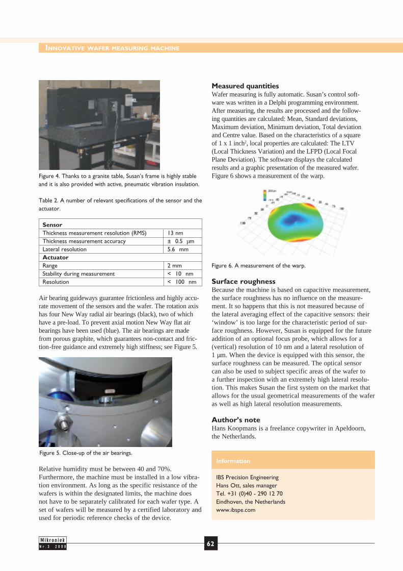
N r . 3 2 0 0 8 62
Measured quantitiesWafer measuring is fully automatic. Susan’s control soft-ware was written in a Delphi programming environment. After measuring, the results are processed and the follow-ing quantities are calculated: Mean, Standard deviations, Maximum deviation, Minimum deviation, Total deviation and Centre value. Based on the characteristics of a square of 1 x 1 inch2, local properties are calculated: The LTV (Local Thickness Variation) and the LFPD (Local Focal Plane Deviation). The software displays the calculated results and a graphic presentation of the measured wafer. Figure 6 shows a measurement of the warp.
Figure 6. A measurement of the warp.
Surface roughnessBecause the machine is based on capacitive measurement, the surface roughness has no influence on the measure-ment. It so happens that this is not measured because of the lateral averaging effect of the capacitive sensors: their ‘window’ is too large for the characteristic period of sur-face roughness. However, Susan is equipped for the future addition of an optional focus probe, which allows for a (vertical) resolution of 10 nm and a lateral resolution of 1 µm. When the device is equipped with this sensor, the surface roughness can be measured. The optical sensor can also be used to subject specific areas of the wafer to a further inspection with an extremely high lateral resolu-tion. This makes Susan the first system on the market that allows for the usual geometrical measurements of the wafer as well as high lateral resolution measurements.
Author’s noteHans Koopmans is a freelance copywriter in Apeldoorn, the Netherlands.
Figure 4. Thanks to a granite table, Susan’s frame is highly stableand it is also provided with active, pneumatic vibration insulation.
Table 2. A number of relevant specifications of the sensor and the actuator.
Sensor Thickness measurement resolution (RMS) 13 nm Thickness measurement accuracy ± 0.5 µm Lateral resolution 5.6 mm Actuator Range 2 mm Stability during measurement < 10 nm Resolution < 100 nm
Air bearing guideways guarantee frictionless and highly accu-rate movement of the sensors and the wafer. The rotation axis has four New Way radial air bearings (black), two of which have a pre-load. To prevent axial motion New Way flat air bearings have been used (blue). The air bearings are made from porous graphite, which guarantees non-contact and fric-tion -free guidance and extremely high stiffness; see Figure 5.
Relative humidity must be between 40 and 70%. Furthermore, the machine must be installed in a low vibra-tion environment. As long as the specific resistance of the wafers is within the designated limits, the machine does not have to be separately calibrated for each wafer type. A set of wafers will be measured by a certified laboratory and used for periodic reference checks of the device.
IBS Precision EngineeringHans Ott, sales managerTel. +31 (0)40 - 290 12 70Eindhoven, the Netherlandswww.ibspe.com
InformationFigure 5. Close-up of the air bearings.
INNOVATIVE WAFER MEASURING MACHINE
60_62susan_nr3_2008.indd 6260_62susan_nr3_2008.indd 62 06-06-2008 13:09:3606-06-2008 13:09:36
Within the Business Unit Advanced Precision and Production Equipment(APPE) precision technology is a familiar term. What about a highlyaccurate spectrometer that orbits in space for many years in extremeconditions and can continue to spot the polluted air in your backgarden? We can provide solutions for these and more issues with thelevel of accuracy that is representative not only of our field but also ofour customer focus.
TNO Science and Industry
TNO.NL
The face of ...
00_Omslag_nr3_2008.indd 6300_Omslag_nr3_2008.indd 63 06-06-2008 12:06:4506-06-2008 12:06:45

In the chip industry, globalization is no mere buzzword. It’s a fact. A business fact that is creating manufac-turing sites all over the world. The question now is, “How to expand operations with logistical technological support?” When it comes to precision metrology, the answer lies within HEIDENHAIN’s worldwide agency network. For linear and angular encoders, support personnel and the answers to meet whatever new challenges the industry throws your way, our worldwide network assures you HEIDENHAIN precision will always be close at hand. No matter where you find your -self. HEIDENHAIN NEDERLAND B.V., Postbus 92, 6710 BB Ede, Tel.: (0318) 581800, Fax: (0318) 581870, www.heidenhain.nl, E-Mail: [email protected]
How Can Semiconductor Manufacturers Find Precision Virtually Anywhere in the World?
angle encoders linear encoders contouring controls digital readouts length gauges rotary encoders
00_Omslag_nr3_2008.indd 6400_Omslag_nr3_2008.indd 64 06-06-2008 12:06:3506-06-2008 12:06:35