mikrobus™ interface board hw reference manual · the mikro us™ interface board connects to the...
TRANSCRIPT

VEST-MIB-USG-001, REV A.0.0
Page 1 APC Proprietary Information June 10, 2016
mikroBUS™ Interface Board HW Reference Manual
VEST-MIB-USG-001
Copyright © 2016 Advanced Products Corporation Pte Ltd. All rights reserved. No part of this document may be photocopied, reproduced, or translated to another language without the prior written permission of Advanced Products Corporation Pte Ltd.

VEST-MIB-USG-001, REV A.0.0
Page 2 APC Proprietary Information June 10, 2016
TABLE OF CONTENTS 1 Overview .........................................................................................................................................5
1.1 Introduction ........................................................................................................................................ 5 1.2 List Of Acronyms ................................................................................................................................. 5 1.3 Reference Documents ........................................................................................................................ 5
2 System Architecture .........................................................................................................................6
2.1 mikroBUS™ Interface Board Pinout .................................................................................................... 7
3 HARDWARE SPECIFICATION .............................................................................................................8
3.1 mikroBUS™ interface board Specification .......................................................................................... 8 3.2 mikroBUS™ UART Socket Interface connectors (J300/301) ............................................................... 8 3.3 mikroBUS™ SPI Socket Interface connectors (J309/310, J315/316) .................................................. 8 3.4 mikroBUS™ I2C Socket Interface connectors (J326/327,J302/303,J311/312,J317/318,J328/329) ... 9 3.5 mikroBUS™ One Wire Socket Interface connectors (J304/305)......................................................... 9 3.6 GPIO Socket Interface connectors (J319/320) ................................................................................... 9 3.7 PINOUT OF 50 WAY INTERFACE CONNECTOR (J200) ....................................................................... 10 3.8 INTERNAL USAGE CONNECTORS ...................................................................................................... 11
4 mikroBUS™ Interface Board Main components ............................................................................... 12
4.1 CONNECTORS AND SWITCHES .......................................................................................................... 12 4.2 CONFIGURATION .............................................................................................................................. 12
4.2.1 Switches .................................................................................................................................... 12 4.2.2 LEDs .......................................................................................................................................... 13
5 Revision History ............................................................................................................................. 14
6 Legal Notices ................................................................................................................................. 15

VEST-MIB-USG-001, REV A.0.0
Page 3 APC Proprietary Information June 10, 2016
LIST OF TABLES
Table 3-1: mikroBUS™ Interface Board Specification......................................................................................... 8 Table 3-2: mikroBUS™ UART Socket Interface Connectors Specification .......................................................... 8 Table 3-3: mikroBUS™ SPI Socket Interface Connectors Specification .............................................................. 8 Table 3-4: mikroBUS™ I2C Socket Interface Connectors Specification .............................................................. 9 Table 3-5: mikroBUS™ One Wire Socket Interface Connectors Specification .................................................... 9 Table 3-6: GPIO Socket Interface Connectors Specification ............................................................................... 9 Table 3-7: Pinout of 50 Way Interface Connector ............................................................................................ 11 Table 4-1: Switches Configuration .................................................................................................................... 13 Table 4-2: LEDs Function .................................................................................................................................. 13

VEST-MIB-USG-001, REV A.0.0
Page 4 APC Proprietary Information June 10, 2016
LIST OF FIGURES/DIAGRAMS Figure 1-1: mikroBUS™ interface board in Development Platform Ecosystem ................................................. 5 Figure 2-1: mikroBUS™ interface board Block Diagram System ........................................................................ 6 Figure 2-2: mikroBUS™ Pinout ........................................................................................................................... 7 Figure 3-1: J319, J320 Pinout Locations ............................................................................................................. 9 Figure 4-1: mikroBUS™ Interface Board ........................................................................................................... 12

VEST-MIB-USG-001, REV A.0.0
Page 5 APC Proprietary Information June 10, 2016
OVERVIEW 1.1 INTRODUCTION This document is the Hardware Reference Manual for mikroBUS™ interface board. The mikroBUS™ interface board supports multiple mikroBUS™ compatible devices and various peripherals for VK series development kits. The VK series development kits refer to VK8100, and VK5100 development kit etc. The mikroBUS™ interface board provides the flexibility to add new functionalities and features to VK series development platform with minimum hardware adjustment.
The mikroBUS™ interface board connects to the VK series development platforms through a 50 way cable. Please refer to the figure below.
Figure 2-1: mikroBUS™ interface board in Development Platform Ecosystem
1.2 LIST OF ACRONYMS Acronym Abbreviation
VEST Venture Embedded Solutions Technology
APC Advanced Products Corporation Private Limited
ISO International Organization for Standardization
DcDK Device Control Development Kit
1.3 REFERENCE DOCUMENTS VEST-DCDK-QSG-001.doc
VEST-MIB-SCH-001.pdf

VEST-MIB-USG-001, REV A.0.0
Page 6 APC Proprietary Information June 10, 2016
2 SYSTEM ARCHITECTURE
Below is the block diagram of the mikroBUS™ interface board connecting to VK series platform through a 50 way cable.
Figure 2-1: mikroBUS™ interface board Block Diagram System
The mikroBUS™ interface board has the following communication ports available :
a. 9 standard mikroBUS™ sockets which consists of UART(x1), SPI (x2), I2C (x5) and 1-wire (x1). Please
refer to the website http://www.mikroe.com/mikrobus/ for more details.
b. One GPIO port
c. Peripherals ie RS232 (DCE mode) and RS232(DTE) selectable, RS485 and CANbus.

VEST-MIB-USG-001, REV A.0.0
Page 7 APC Proprietary Information June 10, 2016
2.1 MIKROBUS™ INTERFACE BOARD PINOUT
Figure 2-2: mikroBUS™ Pinout
The mikroBUS™ pinout is shown above with the combination of two 1x8 female headers. In mikroBUS™ interface board, mikroBUS™ compatible host connectors are mainly provided to support Click Boards by MikroElektronika and they are categorized to UART, SPI, I2C and 1-wire interface where users connect the Click board accordingly depending on its communication interface. The unused interface is left no connection in each mikroBUS™ connector.
The 3 communication interfaces (UART, SPI, I2C) are connected to VK series development kit directly while for 1-wire bus, a 1-wire-to-I2C converter is inserted to support it through I2C.

VEST-MIB-USG-001, REV A.0.0
Page 8 APC Proprietary Information June 10, 2016
3 HARDWARE SPECIFICATION
3.1 MIKROBUS™ INTERFACE BOARD SPECIFICATION This section covers the specifications and features of the board and provides a high level description of the major components and interfaces that make up the board.
Feature Description
Operating Conditions 3.3V or 5V
MCU N/A
Power Source From VK series development kit
LDO N/A
Supported Boards 1. Click boards by MikroElektronika 2. mikroBUS™ compatible boards 3. GPIO Board
Supported Ports 4. RS232 (DTE or DCE mode selectable) 5. RS485 6. CAN Bus
No. of Functional Card Slots 10
PCB 4-layer Board
Serial Port RS232 and RS485
(RS232 is connected via DSUB9 while RS485 via RJ45)
CAN Bus RJ10 Connector
(CAN protocol, CAN1.2, CAN 2.0 and CANopen)
Table 3-1: mikroBUS™ Interface Board Specification
3.2 MIKROBUS™ UART SOCKET INTERFACE CONNECTORS (J300/301) This section covers the electrical specifications of the mikroBUS™ UART socket interface connectors.
Feature Description
Operating Voltage 3.3V+/-10%
UART_TXD Transmitter TTL/CMOS level Output
UART_RXD Receiver TTL/CMOS Input
UART_RTS UART RTS TTL/CMOS level Output
UART_CTS UART CTS TTL/CMOS level Input Table 3-2: mikroBUS™ UART Socket Interface Connectors Specification
3.3 MIKROBUS™ SPI SOCKET INTERFACE CONNECTORS (J309/310, J315/316) This section covers the electrical specifications of the mikroBUS™ SPI socket interface connectors. The SPI interface will support up to two SPI slave ports. Control signal SPI_SS0 selects the port 0 while SPI_SS1 selects the port 1.
Feature Description
Operating Voltage 3.3V+/-10%
SPI_SCLK SPI Clock Output
SPI_MOSI SPI Master Output, Slave Input
SPI_MISO SPI Master Input, Slave Output
SPI_SS0 SPI Port 0 Select
SPI_SS1 SPI Port 1 Select
Table 3-3: mikroBUS™ SPI Socket Interface Connectors Specification
VEST-MIB-USG-001, REV A.0.0
Page 9 APC Proprietary Information June 10, 2016
3.4 MIKROBUS™ I2C SOCKET INTERFACE CONNECTORS
(J326/327,J302/303,J311/312,J317/318,J328/329) This section covers the electrical specifications of the mikroBUS™ I2C socket interface connectors. The I2C interface will support up to five I2C device ports. That means all the five device ports share the same I2C clock and data bus.
Feature Description
Operating Voltage 3.3V+/-10%
I2C_SCL I2C Clock Output
I2C_SDA I2C Data Input/ Output
Table 3-4: mikroBUS™ I2C Socket Interface Connectors Specification
3.5 MIKROBUS™ ONE WIRE SOCKET INTERFACE CONNECTORS (J304/305) This section covers the electrical specifications of the mikroBUS™ One Wire socket interface connectors. There is a 1-wire-to-I2C converter IC inserted to support it through I2C bus.
Feature Description
Operating Voltage 3.3V+/-10%
CLICK_AN9 One Wire I/O
CLICK_PWM9 One Wire I/O
CLICK_RST9 One Wire I/O
CLICK_INT9 One Wire I/O
CLICK_CS9 One Wire I/O Table 3-5: mikroBUS™ One Wire Socket Interface Connectors Specification
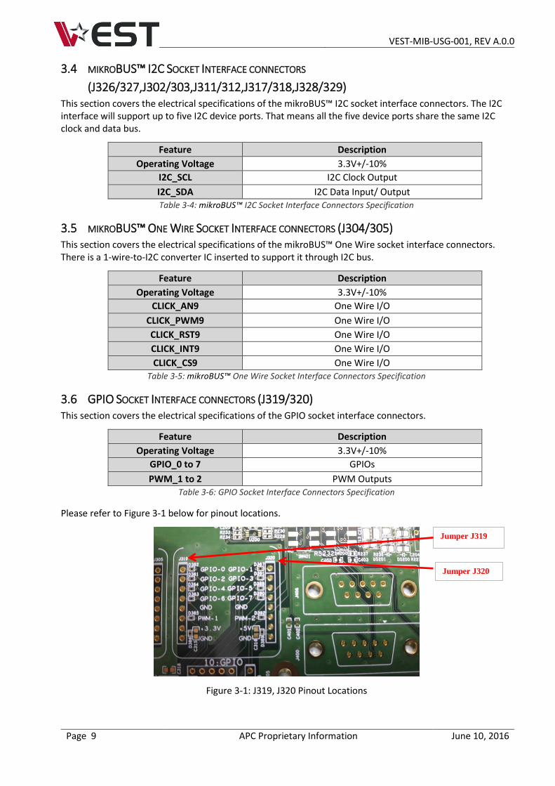
3.6 GPIO SOCKET INTERFACE CONNECTORS (J319/320) This section covers the electrical specifications of the GPIO socket interface connectors.
Feature Description
Operating Voltage 3.3V+/-10%
GPIO_0 to 7 GPIOs
PWM_1 to 2 PWM Outputs Table 3-6: GPIO Socket Interface Connectors Specification
Please refer to Figure 3-1 below for pinout locations.
Figure 3-1: J319, J320 Pinout Locations
Jumper J319
Jumper J320

VEST-MIB-USG-001, REV A.0.0
Page 10 APC Proprietary Information June 10, 2016
3.7 PINOUT OF 50 WAY INTERFACE CONNECTOR (J200) Pin Number Pin Name Description
1 GND Ground
2 GND Ground
3 SPI_SCK SPI Clock
4 SPI1_MOSI SPI MOSI
5 SPI1_MISO SPI MISO
6 SPI_SS0 SPI Chip Select 0 (Active Low)
7 SPI_SS1 SPI Chip Select 1 (Active Low)
8 GND Ground
9 I2C_SCL I2C Clock
10 I2C_SDA I2C Data
11 GND Ground
12 UART_CTS RS232 CTS
13 UART_RTS RS232 RTS
14 UART_TXD RS232 TXD
15 UART_RXD RS232 RXD
16 GND Ground
17 CAN_H CAN Bus Data Signal
18 CAN_L CAN Bus Data Signal
19 GND Ground
20 GPIO_0 General Purpose Input/Output
21 GPIO_1 General Purpose Input/Output
22 GND Ground
23 GPIO_2 General Purpose Input/Output
24 GPIO_3 General Purpose Input/Output
25 GPIO_4 General Purpose Input/Output
26 GND Ground
27 GPIO_5 General Purpose Input/Output
28 GPIO_6 General Purpose Input/Output
29 GPIO_7 General Purpose Input/Output
30 GND Ground
31 PWM1 Pulse Width Modulation 1
32 GND Ground
33 PWM2 Pulse Width Modulation 2
34 GND Ground
35 V5P0 5-V Power Supply
36 V5P0 5-V Power Supply
37 V5P0 5-V Power Supply
38 GND Ground
39 GND Ground
40 GND Ground
41 V3P3 3.3-V Power Supply
42 V3P3 3.3-V Power Supply
43 V3P3 3.3-V Power Supply
44 RSV1 Reserved

VEST-MIB-USG-001, REV A.0.0
Page 11 APC Proprietary Information June 10, 2016
45 GND Ground
46 GND Ground
47 RS485_DP RS485 Data Signal
48 RS85_DN RS485 Data Signal
49 GND Ground
50 GND Ground Table 3-7: Pinout of 50 Way Interface Connector
3.8 INTERNAL USAGE CONNECTORS The connectors listed below are for internal measurement and debugging purposes.
J306, J307, J308, J313, J314, J321, J322, J323, J324, J325, J330, J331, J332

VEST-MIB-USG-001, REV A.0.0
Page 12 APC Proprietary Information June 10, 2016
4 MIKROBUS™ INTERFACE BOARD MAIN COMPONENTS
This section describes the key components on the board. It provides information on their location and function.
4.1 CONNECTORS AND SWITCHES The picture below shows the locations of the connectors and switches on the PCB. There are total 10 card slots available where 9 slots are mikroBUS™ compatible and 1 slot is for GPIOs.
Figure 4-1: mikroBUS™ Interface Board
Interface connector is the interface with VK series development platform
Click (UART) supports Click Board with UART communication
Click (SPI1/2) supports Click Board with SPI communication
Click (I2C1~5) supports Click Board with I2C communication
Click (1-wire) supports Click Board that needs 1-wire bus
GPIO provides users a slot to design own board for GPIO application.
RS232(DTE) is a DB-9 male connector which supports the serial communication to ViO platform
RS232(DCE) is a DB-9 female connector which supports the serial communication to PC platform
RS485 is a RJ45 connector which supports the serial communication to VK series development
platform
CAN is a RJ10 connector which supports the CAN Bus communication to VK series development
platform
SW200 is to select the usage of Click Board (UART) or RS232 port
SW401 is to select the usage of RS232(DTE mode) or RS232 (DCE mode)
4.2 CONFIGURATION
4.2.1 Switches There are some settings to be configured before boot up. Table below shows the configuration setting by switches.
Click (UART)
CAN
RS232(DTE)
RS232(DCE)
SW2
00
Interface Connector
SW401
Click
(SPI1) Click (SPI2)
Click (I2C1)
Click (I2C2)
Click (I2C3)
Click (I2C4)
Click (I2C5)
Click (1-WIRE)
GPIO

VEST-MIB-USG-001, REV A.0.0
Page 13 APC Proprietary Information June 10, 2016
Switches Pos A (slide to top position) Pos B (slide to bottom position)
SW200 UART RS232
SW401 RS232 (DCE) RS232 (DTE)
Table 4-1: Switches Configuration
The interface for Click Board – UART is shared with RS232 Port where SW200 would be used to choose which path to go.
SW401 is to select between RS232 (DCE) and RS232 (DTE) for RS232 serial communication.
4.2.2 LEDs Below table shows the function of LEDs.
LED Function Description
DS200 Power indicator LED turns on when 3.3-V power is in.
DS201 Power indicator LED turns on when 5-V power is in.
Table 4-2: LEDs Function
VEST-MIB-USG-001, REV A.0.0
Page 14 APC Proprietary Information June 10, 2016
5 REVISION HISTORY
Version Date Released Changes
A June 10, 2016 First Official Release

VEST-MIB-USG-001, REV A.0.0
Page 15 APC Proprietary Information June 10, 2016
6 LEGAL NOTICES
The signed agreement between Purchaser and APC will govern the sale and purchase of APC’s Venture Embedded Solutions Technology (“VEST”) products (“Products”). In the event that no agreement has been concluded, APC’s terms and conditions of supply will apply.
Testing and other quality control techniques are used to the extent that APC deems necessary to support its warranty.
Except where required by law, specific testing of all parameters of each Product is not necessarily performed.
Purchaser must provide adequate design and operating safeguards to minimize inherent or procedural and technical risks associated with Purchaser products and applications. Purchaser is solely responsible for its selection and use of APC Products. APC assumes no liability for applications assistance, Purchaser product design or any incompatibility of the Product with Purchaser product.
Products supplied by APC are not designed, intended or authorized for use in life support, life sustaining, medical systems or devices, aircraft navigation, nuclear, or other applications, including, but not limited to, public transportation operating systems, in which the failure of such Products could reasonably be expected to result in personal injury, loss of life or severe property or environmental damage. Purchaser acknowledges that use of APC’s Products in such product applications is understood to be fully at the risk of Purchaser and that Purchaser is responsible for verification and validation of the suitability of APC’s Products in such applications. Purchaser agrees that APC is not and shall not be liable, in whole or in part, for any claim or damage arising from use in such applications. Purchaser agrees to indemnify, defend and hold APC harmless from and against any and all claims, damages, losses, costs, expenses and liabilities arising out of or in connection with any such use or application.
APC retains all rights to all proprietary intellectual property in the Products and associated manufacturing processes and has the right to file for and obtain intellectual property protection for same.