migration guide - orcad · migration guide migrating from pads to orcad pcb designer. 2 ... logic...
TRANSCRIPT

1
Migrating from PADS to OrCAD PCB Designer
Migration GuideMigrating from PADS to OrCAD PCB Designer

2
Migrating from PADS to OrCAD PCB Designer
Table of Contents
Overview . . . . . . . . . . . . . . . . . . . . . . . . . . . . . . . . . . . . . . . . . . . . . . . . . . . . . . . . . . . .3
Import Your PADS Schematic Data to OrCAD Capture . . . . . . . . . . . . . . . . . . . . . . . . . . .4
Import Your PADS PCB Data to OrCAD PCB Editor . . . . . . . . . . . . . . . . . . . . . . . . . . . . .5
Making the PCB Database Fully Compliant to OrCAD PCB Editor . . . . . . . . . . . . . . . . . .8
Synchronizing the Schematic to the Migrated PCB . . . . . . . . . . . . . . . . . . . . . . . . . . . .10
Importing Your PADS PCB Libraries into OrCAD PCB Editor . . . . . . . . . . . . . . . . . . . . . .10
Next Steps . . . . . . . . . . . . . . . . . . . . . . . . . . . . . . . . . . . . . . . . . . . . . . . . . . . . . . . . . .12

3
Migrating from PADS to OrCAD PCB Designer
Overview
Choosing the right PCB design solution is never an easy task . No matter if you are a startup company looking for tools to develop your first product, a large enterprise wanting to improve the productivity and efficiency of your design team, or somewhere in between, selecting a PCB solution can be a daunting task . Nobody wants to get 75% of the way through a design to find that the software you selected is not going to achieve what you need it to do .
There are many aspects you have to consider when choosing your PCB Design solution including:
• Do the capabilities of the offering and its technology meet your design requirements?
• What’s the cost of the software? Does it fit within your budget?
• What’s the support service like? Will you be able to get quick responses to your questions and access online based tutorials?
• Can its technology and solution scale with your needs? As designs are getting more and more complex, will the capabilities of the tool adjust accordingly?
• How many other companies in your industry are using this tool and what is their feedback?
With OrCAD® PCB Design Solutions, you can be confident that you will have the right solution and technol-ogies to meet all of your design challenges today and tomorrow . Here are five of many reasons why:
Reason 1: Security of Scalability for Your Future Design Challenge
Cadence and OrCAD provide the only full scalable PCB design solution on the market that can seamlessly grow with your needs . Invest for the future with a tool that can grow as your business does .
Reason 2: Affordable Price and Flexible Purchase Models
OrCAD provides flexible pricing tiers enabling design teams to access the capabilities they need for the price they can afford .
Reason 3: Cutting-edge Technologies
OrCAD offers constraint-driven design, advanced auto/interactive routing, high-speed design, DFM, dynamic shape technology, and much more, helping you deliver high-quality, first-time-right designs in the shortest timeframes .
Reason 4: Fully Customizable and Ecosystem Empowered
Open APIs allow you to extend and customize your design environment to meet your unique needs . Connect to external systems, generate custom reports, even customize the UI . It is all possible with OrCAD .
Reason 5: Industry’s Best Customer Support
OrCAD products are backed by Cadence and their network or certified Cadence Channel Partners (CCP) . Get help when you need it by phone or email from local, knowledgeable PCB design professionals .
Like many companies selecting OrCAD PCB Design Solutions, you may have existing or legacy designs you need to convert or translate into an appropriate design format . The good news is that these OrCAD tools are supplied with an integrated and proven PADS design translator built in .
This guide will walk you through the steps and process involved in getting your design IP into the OrCAD format so you can start realizing the advantages of moving to OrCAD!

4
Migrating from PADS to OrCAD PCB Designer
Import Your PADS Schematic Data to OrCAD Capture
Step 1 – Export schematic data from PADS.
In DX Designer export your PADS schematic to EDIF 2.0 format using the EDIF Interface:
Note: If you are using PADS Logic you will need to convert your design into DxDesigner first using the Mentor supplied conversion utilities then you can proceed with step 1 of the conversion process .
Step 2 – Import schematic data to OrCAD Capture.
Once the EDIF file is created, launch OrCAD Capture and use the File >> Import Design option and select the EDIF Tab for Import of your PADS EDIF file:
Your PADS DX Schematic has now been migrated . Some text cleanup may be required .

5
Migrating from PADS to OrCAD PCB Designer
Import Your PADS PCB Data to OrCAD PCB Editor
Step 1 - Preparing your PADS PCB database for migration.
In the PADS PCB tool, export your PCB database to a Version 2005 ASCII format:
This creates a V2005 ASCII database (* .ASC) we use for translation .
Note: Only copper pours in PADS defined as positive data are recognized by the translator .
Step 2 - Import your PADS PCB design into OrCAD PCB Editor.
Use File >> New Drawing to create a new board database:

6
Migrating from PADS to OrCAD PCB Designer
Next import your PADS PCB ASCII database:
Step 3 - Layer mapping your data into OrCAD PCB Editor.
Select your ASCII database for Import, enter an options file name and select “Show Options Dialog” to create your options file, then select “Translate”:
Map PADS layer numbers to the corresponding OrCAD PCB Editor layers (PCB footprint, board data layers, etch):

7
Migrating from PADS to OrCAD PCB Designer
Once the translation is complete, open the database with File >> Open and select the newly translated PCB database .
Step 4 - Checking the imported database for design errors.
Next check the database for errors using the command Tools >> Database Check:
DBDoctor purges redundant vias and fixes any database errors found shown here in the viewlog:
8
Migrating from PADS to OrCAD PCB Designer
Making the PCB Database Fully Compliant to OrCAD PCB Editor
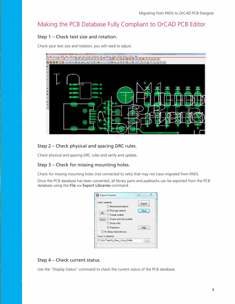
Step 1 – Check text size and rotation.
Check your text size and rotation, you will need to adjust .
Step 2 – Check physical and spacing DRC rules.
Check physical and spacing DRC rules and verify and update .
Step 3 – Check for missing mounting holes.
Check for missing mounting holes (not connected to nets) that may not have migrated from PADS .
Once the PCB database has been converted, all library parts and padstacks can be exported from the PCB database using the File >> Export Libraries command .
Step 4 – Check current status.
Use the “Display Status” command to check the current status of the PCB database .

9
Migrating from PADS to OrCAD PCB Designer
Step 5 – Check for disconnected nets.
Check for disconnected nets (These are usually connect lines that are not snapped to pin center) .
Step 6 – Check boundary-courtyard violations.
Review and waive any package-to-package boundary-courtyard violations . (Assuming placement was previ-ously verified in PADS .)
Your migration from PADS PCB Design to OrCAD PCB Editor should now be complete .

10
Migrating from PADS to OrCAD PCB Designer
Synchronizing the Schematic to the Migrated PCB
If you plan to translate a complete project that includes the PCB design into OrCAD design environment, first of all, open the migrated schematic design in OrCAD Capture .
To synchronize the schematic to the migrated PCB database, create a new netlist using the migrated PCB database as the input design .
Note: Duplicate pin names (other than PWR or GND designated pins) must be resolved .
Logic symbols and PCB footprint pin mismatches may need to be corrected . (This occurs when unused pins on the logic symbols are not accounted for with no-connect property .)
Once the schematic has been synchronized to the integrated PCB, cross-probing and cross-placement tools can be utilized .
Importing Your PADS PCB Libraries into OrCAD PCB Editor
Invoke the library translator from within OrCAD PCB Editor:

11
Migrating from PADS to OrCAD PCB Designer
Use the OrCAD library translator to browse to the folder where your PADS package and decal libraries are located, and specify your desired output folder for the migration . Type in the file name for the options file you wish to create, select the “Show Options Dialog”, and then “Translate”:
Select the options below:
The OrCAD footprint library parts and padstacks are created as shown here:

12
Migrating from PADS to OrCAD PCB Designer
Next Steps
Now that you know how easy it is to move to OrCAD PCB Designer, are you ready to learn more about the exciting OrCAD features and technologies which will help you improve your design productivity? Here are some resources you can leverage to learn more about OrCAD technologies .
What’s New in OrCAD
Want to know what are the new features in the latest OrCAD release? Check out what’s new .
Customer Testimonials
See how real companies are leveraging OrCAD to bring their products to market on time and on budget . View OrCAD customer stories .
Product Information
Need more videos, app notes, datasheets to dive deeper into the OrCAD technologies? View OrCAD product pages .
Ready to Talk?
The OrCAD product line is supported by a worldwide network of Cadence Channel Partners (CCP) . Would you like to talk with our channel partners? Contact us now!
© 2016 Cadence Design Systems, Inc . All rights reserved worldwide . Cadence, the Cadence logo, and OrCAD are registered trade-marks of Cadence Design Systems, Inc . in the United States and other countries . All other trademarks are the property of their respective owners .
The OrCAD product line is owned by Cadence Design Systems, Inc .