mid-ir broadband supercontinuum generation from a...
TRANSCRIPT
Mid-IR broadband supercontinuum generationfrom a suspended silicon waveguideRAI KOU,1,4,* TAIKI HATAKEYAMA,2 JASON HORNG,1 JI-HUN KANG,1 YUAN WANG,2,4
XIANG ZHANG,2,3,5 AND FENG WANG1,3,6
1Department of Physics, University of California at Berkeley, Berkeley, California 94720, USA2Nanoscale Science and Engineering Center, University of California, Berkeley, California 94720, USA3Materials Sciences Division, Lawrence Berkeley National Laboratory, Berkeley, California 94720, USA4Currently at National Institute of Advanced Industrial Science and Technology (AIST), Tsukuba, Ibaraki, 305-8569, Japan5e-mail: [email protected]: [email protected]*Corresponding author: [email protected]
Received 14 December 2017; revised 13 February 2018; accepted 14 February 2018; posted 16 February 2018 (Doc. ID 315728);published 14 March 2018
Mid-infrared light provides numerous unexpected oppor-tunities in scientific discoveries because this wavelengthregion covers the fingerprints of various molecular vibra-tional resonances. However, the light generation efficiencyand bandwidth have been a long-standing bottleneck whichhas limited the development so far. Moreover, the lightsource that can be integrated with other components suchas wavelength filters, detectors, and electronics, will be thekey factor toward the future practical applications. Here, wepropose an all-air-cladding silicon-rib waveguide to exper-imentally reveal the nonlinear performance of supercon-tinuum generation. By tuning the waveguide dispersionparameters with simulation, a continuous broad spectrumof 1.32 octave (2–5 μm) was observed with a pump pulsewavelength of 4 μm. To further investigate our device char-acteristics, multiple conditions were set by varying theinteraction length, pump power, and waveguide dimension,which revealed the nonlinear phenomenon in thewaveguide. © 2018 Optical Society of America
OCIS codes: (190.4360) Nonlinear optics, devices; (320.6629)
Supercontinuum generation; (130.3060) Infrared.
https://doi.org/10.1364/OL.43.001387
Silicon, a promising electronic material for more than half acentury, has recently gained importance as an optical material.As predicted by Soref in his Si-based optoelectronic integratedcircuit prediction [1], this material with germanium has beenattracting attention in “silicon photonics” since the beginningof this century. The distinctive features of a complementarymetal oxide semiconductor (CMOS)-compatible process openeda new world of high-performance optoelectronic circuits withextremely low fabrication cost. However, most applicationshave been developed for near-infrared (IR) telecommunicationbands around an optical wavelength of 1.5 μm so far, even
though this material has an excellent transparency window overIR and terahertz bands [2–4]. If a broadband supercontinuum(SC) light source can be generated in such an integrated opticalcircuit, it will be able to open up possibilities for various ap-plications such as environmental measurement [5], bio-chemicalsensing [6], metrology [7], optical communication [8], and ab-sorption spectroscopy in basic science [9]. Furthermore, recentadvanced technology of chalcogenide glass-based fibers [10,11]and waveguides [12] generate SC lights very efficiently andbroadly, but the future compatibility with electronics integra-tion is still difficult. Previous challenges of the SC light genera-tion from the group IV materials began at a 1.5 μm pump witha standard silicon wire waveguide [13,14], and then graduallyextended to a longer wavelength up to a mid-infrared (mid-IR)regime recently. Thanks to the material nature of silicon, thelarge optical linear susceptibility allows a tight guiding-modeconfinement as small as a sub-μm2 cross-sectional area, andthe remarkably large third-order nonlinear susceptibility ena-bles an efficient SC light generation induced by multi-complexlight-matter interactions such as self-phase modulation (SPM),cross-phase modulation, four-wave mixing, self-steepening,stimulated Raman scattering (SRS), Cherenkov radiation, andsoliton fission. It should be noted that the Kerr coefficientn2;Si in bulk crystalline silicon has been reported as 4.2 ×10⁻¹⁸ m2∕W [15,16] which is about 20 times larger in valuethan silicon nitride [17], and more than 160 times larger thansilica glass [18] around a wavelength of 1.5 μm. Moreover, ahighly confined waveguide due to silicon’s high refractive indexallows large anomalous dispersion that can maintain a veryshort pulse duration by counterbalancing the SPM effect. Sucha dispersion-induced pulse compression effect, which can berealized by tuning the waveguide dimensions, creates strongpeak power and leads to efficient SC generation. Reducingmulti-photon absorption is also a remarkable advantage whenmoving the wavelength range of interest to the mid-IR region.While the Kerr coefficient n2;Si does not change by orders ofmagnitude as the wavelength becomes longer, the multi-photon
Letter Vol. 43, No. 6 / 15 March 2018 / Optics Letters 1387
0146-9592/18/061387-04 Journal © 2018 Optical Society of America

absorption such as two-photon absorption and three-photonabsorption can be greatly suppressed [19–21].
According to the latest updates related to the SC generationin mid-IR, an octave-spanning SC light ranging from 1.5 to3.6 μm [22] and a frequency comb ranging from 1.5 to 3.2 μm[23] using a standard silicon-channel waveguide have beendemonstrated. The limited spectral performance is restrictedby the strong absorption edge due to a Si-O-Si vibrationalmode from around 2 μm (e.g., absorption index k reaches∼10−4 at 4 μm and ∼10−2 at 5 μm) and the presence of OHgroups at wavelengths of 2.73–2.85, 3.5, and 4.3 μm [24].(Note that the absorption rate depends greatly on the samplepreparation methods.) In another report, over 1.5 octave SCspectrum covering from 2.0 to 5.6 μm with a silicon-on-sapphire platform [25] has been achieved. Although the sap-phire cladding has a wider transparent window compared tosilicon dioxide, the absorption coefficient is continuously risingbeyond 5 μm [26]. To overcome these restrictions, we demon-strate a suspended all-air-cladding silicon waveguide to generateSC light in the mid-IR range. This structure no longer requiresa special wafer-bonding process that causes a cost increase andincompatibility with the standard CMOS process. In fact, sev-eral groups have predicted an efficient SC generation from anysuspended Si, Ge, or SiGe waveguides by theoretical analysis[25,27,28], but the experimental demonstration has not beenreported. According to the past research, several different typesof transparent silicon waveguides have been proposed for themid-IR wavelength such as a suspended structure fabricatedby wafer boding [29] or wet etching [30], and low-loss platformenabled by mode-distribution adjustment [31]. In this Letter,we selected the wet etching method because of the design flex-ibility of the waveguide dimension, as well as wavelengthdispersion and relatively simple fabrication procedures.
Figure 1(a) shows the schematic illustration of the sus-pended waveguide. The thicknesses of the waveguide (H ), slab(S), and buried oxide were 2 μm, 500 nm, and 3 μm, respec-tively. There were 1 μm × 2 μm holes around the waveguidefor wet etching. The distance between the waveguide andthe hole was 4 μm. The waveguide was fabricated on a SOIsubstrate. The device layer was grown by the floating-zonemethod to minimize free carrier absorption. The pattern waswritten by an e-beam lithography machine and transferredto the substrate by reactive ion etching (RIE). The holes aroundthe waveguide were made by e-beam lithography and RIE proc-esses. After making the holes, the substrate was dipped in 5∶1buffered hydrofluoric acid (BHF) to remove the oxide layer be-low the waveguide. Figure 1(b) shows a cross-sectional image ofthe suspended silicon waveguide. The silicon membrane doesnot have a deflection because the slab is thick enough to avoid
the mechanical instability. If the thickness of slab is less than500 nm, the suspended waveguide would bend down to thesubstrate. The deflection of the beam at the center point is de-scribed by Fl 3∕4ES3, where F is the force on the center of thebeam, and l is the length of the beam between the supports.E represents Young’s modulus of silicon. Given that the force isapplied only by the weight of the waveguide, the maximumdeflection by the force is less than 1 nm. Therefore, the deflec-tion by the weight of the waveguide is negligible. The deflec-tion of the membrane is also caused by the residual stress in thesilicon layer. The deflection induced by the residual stress iswritten by 3Ml2∕4ES3, where M is the bending moment.Thus, the deflection by the residual stress is proportional to S−3.This trend has been experimentally shown in a previous report[20]. It indicates that the thicker membrane has more mecha-nical stability if the residual stress does not change. Besides,Young’s modulus of a silicon membrane becomes lower thanthe bulk silicon when the thickness of the membrane is lessthan 300 nm [21]. For example, Young’s modulus of a 300 nmthick silicon cantilever is 168 GPa, which is the same as thebulk silicon, while Young’s modulus of a 12 nm thick siliconcantilever is 53 GPa. By considering the residual stress andYoung’s modulus of a silicon membrane, we conclude thatour device is mechanically stable compared to thin siliconmembranes (<300 nm).
A flat dispersion in an anomalous regime results in group-velocity-matched light propagation in a short pulse width bybalancing with the SPM effect. We calculated the dispersioncurves for a single mode and tightly confined the rib waveguideswith W:1000–3000 nm ×H:500 nm × S:100 nm [Fig. 2(a)].While the anomalous dispersion reaches up to 900 ps/nm/kmat the narrowest waveguide width (W: 1000 nm), the availablebandwidth was limited due to the mode confinement. (Notethat the positive value in the vertical axis corresponds to the
Fig. 1. (a) Schematic of suspended silicon waveguide. (b) Scanningelectron microscope image of the suspended waveguide.
Fig. 2. Calculated dispersion profiles to compare the difference be-tween thin and thick SOI substrates. (a) With a thin SOI thickness (H)of 500 nm and slab thickness (S) of 100 nm. (b) With a thick SOIthickness (H) of 2000 nm and a slab thickness (S) of 500 nm.
1388 Vol. 43, No. 6 / 15 March 2018 / Optics Letters Letter

anomalous dispersion.) Additionally, both the dispersion andbandwidth are significantly modulated by the dimensions ofthe core, which results in a low tolerance to the fabricationerror. In Fig. 2(b), we designed a relatively large-core wave-guide with dimensions ofW:4000–10000 nm ×H:2000 nm ×S:500 nm to improve the dispersion profiles to be wider andflatter over the mid-IR region. When the thickness of the wave-guide is 2000 nm, the dispersion is not greatly modulated byvarying the width of the waveguide. Thus, our device is notaffected by the fabrication errors compared to the thinner wave-guides. To realize an efficient light coupling, 10 μm wide adia-batic tapers were equipped at both input and output edges.
The experiment setup for SC generation is illustrated inFig. 3. A pump light source is generated by a Yb:KGW pulselaser system followed by an optical parametric amplifier. Theoscillator produces a 300 fs short pulse with a center wave-length of 1028 nm at a repetition rate of 150 kHz. By adjustingthe LiNbO3 crystal angle for a birefringent phase-matchedcondition between the fundamental (λfund:1028 nm) and idler(λidler:1384 nm) beams, a difference-frequency generationwavelength as a pump source (λpump:4000 nm) is generated.The light polarization is adjusted to a quasi-TE mode (parallelto substrate). The femtosecond mid-IR pump pulse is coupledinto the suspended silicon waveguide by using a pair of high-numerical-aperture (NA � 0.85 at input, 0.56 at output)black-diamond (BD) lenses with an anti-reflection coatingfor the 3–5 μm range. To couple the pump light efficiently,a continuous-wave (CW) laser diode (λtracer: ∼ 1500 nm) wasused for imaging the input/output cross sections of the wave-guide by an InGaAs camera, as well as tracing of the mid-IRlight path. For the sample position alignment, a liquid-nitrogen-cooled HgCdTe detector (MCT#1) coupled the output lightdirectly followed by a current-mode transimpedance preampli-fier and a lock-in amplifier. Next, a refractive-grating-based(300 grooves/mm, 2–5 μm design wavelength) monochroma-tor with an MCT#2 was used to perform the spectroscopy in20 nm resolution steps.
We start the device characterization with loss measurementby coupling a CW-LD tracer light. With a waveguide width(W) of 8 μm, a transmittance of 15–20% using two couplinglenses was measured across a 12 mm long device. Next, we mea-sured the loss at the pump wavelength of 4 μm. The couplingefficiency at the input was estimated to be ∼15%. The losscontains the transmittance of a BD lens (50%), Fresnel reflec-tion on the silicon surface, and mode-field mismatching betweenthe incident light and confinement mode (especially due to thewaveguide height). The propagation loss was ∼5 dB∕cm at the
pump wavelength. Taking the maximum input pump intensityof 28.8 mW for an example, the actual coupled power to thewaveguide is around 4.3 mW which corresponds to 96 kW inpeak power and 600 GW∕cm2 in power density. To preventlaunching any higher-order modes coupling we optimized themode-field distribution to be single by monitoring it with anInGaAs camera from the output. At the beginning of the align-ment for SC generation, we used neutral density (ND) filters toattenuate the pump intensity to operate at sub milliwatt level toprotect the device surface from excessive heat. Then the focus-ing position was aligned by iterations to maximize the lighttransmittance from the wavelength of 1.5–4 μm. Figure 4(a)shows the spectra obtained using three input intensity condi-tions of 1.9, 14.9, and 28.6 mW (average power), with a 7 mmlong device. At the maximum input power, a spectrum ranging3.0–4.7 μm was observed at an output intensity of −30 dBlevel. A simple mountain-shaped spectrum suggests that theSPM effect is a dominant nonlinearity that spreads toward bothsides while increasing the pump power. (Note that the sharpabsorption observed at around 4.25 μm was caused by a vibra-tion of asymmetric-bond stretching in CO2.) According toRef. [13], the SRS plays a small role in a crystalline-siliconwaveguide because the gain bandwidth is narrow enough.Next, a 12 mm long device was measured to investigate theinteraction length dependence. Figure 4(b) exhibits the spectrameasured with comparable pump intensity from 1.5 to28.8 mW. Now, we recognized that even with the 1.5 mW,the pumped spectrum induced spectral broadening slightly.As we increase the pump intensity above 10 mW, many smallpeaks were induced due to the soliton fission, which meansdifferent nonlinear broadening mechanisms were observed atthe device lengths of 7 and 12 mm. According to the Ref. [32],the dispersion length LD (� T 2
0∕jβ2j) is ∼100 mm withT 0 � 300 fs, and β2 � −0.85 ps2∕m at 4 μm. The soliton fis-sion point can usually be observed in the range of 10–50% of
Fig. 3. Schematic of the experiment setup. HWP, half-wave plate;DM, dichroic mirror; FM, flip mirror; BS, beam splitter.
Fig. 4. (a) Measured spectra with a 7 mm long device. The averagepumping power was at 1.9, 14.9, and 28.5mW. (b)With a 12mm longdevice, the average pumping power was at 1.5, 12.6, and 28.8 mW.
Letter Vol. 43, No. 6 / 15 March 2018 / Optics Letters 1389
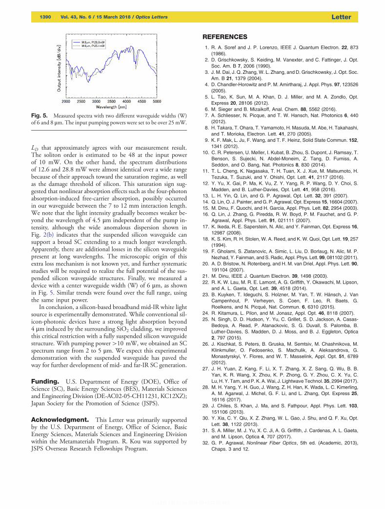
LD that approximately agrees with our measurement result.The soliton order is estimated to be 48 at the input powerof 10 mW. On the other hand, the spectrum distributionsof 12.6 and 28.8 mW were almost identical over a wide rangebecause of their approach toward the saturation regime, as wellas the damage threshold of silicon. This saturation sign sug-gested that nonlinear absorption effects such as the four-photonabsorption-induced free-carrier absorption, possibly occurredin our waveguide between the 7 to 12 mm interaction length.We note that the light intensity gradually becomes weaker be-yond the wavelength of 4.5 μm independent of the pump in-tensity, although the wide anomalous dispersion shown inFig. 2(b) indicates that the suspended silicon waveguide cansupport a broad SC extending to a much longer wavelength.Apparently, there are additional losses in the silicon waveguidepresent at long wavelengths. The microscopic origin of thisextra loss mechanism is not known yet, and further systematicstudies will be required to realize the full potential of the sus-pended silicon waveguide structures. Finally, we measured adevice with a center waveguide width (W) of 6 μm, as shownin Fig. 5. Similar trends were found over the full range, usingthe same input power.
In conclusion, a silicon-based broadband mid-IR white lightsource is experimentally demonstrated. While conventional sil-icon-photonic devices have a strong light absorption beyond4 μm induced by the surrounding SiO2 cladding, we improvedthis critical restriction with a fully suspended silicon waveguidestructure. With pumping power >10 mW, we obtained an SCspectrum range from 2 to 5 μm. We expect this experimentaldemonstration with the suspended waveguide has paved theway for further development of mid- and far-IR SC generation.
Funding. U.S. Department of Energy (DOE), Office ofScience (SC), Basic Energy Sciences (BES), Materials Sciencesand Engineering Division (DE-AC02-05-CH11231, KC12XZ);Japan Society for the Promotion of Science (JSPS).
Acknowledgment. This Letter was primarily supportedby the U.S. Department of Energy, Office of Science, BasicEnergy Sciences, Materials Sciences and Engineering Divisionwithin the Metamaterials Program. R. Kou was supported byJSPS Overseas Research Fellowships Program.
REFERENCES
1. R. A. Soref and J. P. Lorenzo, IEEE J. Quantum Electron. 22, 873(1986).
2. D. Grischkowsky, S. Keiding, M. Vanexter, and C. Fattinger, J. Opt.Soc. Am. B 7, 2006 (1990).
3. J. M. Dai, J. Q. Zhang, W. L. Zhang, and D. Grischkowsky, J. Opt. Soc.Am. B 21, 1379 (2004).
4. D. Chandler-Horowitz and P. M. Amirtharaj, J. Appl. Phys. 97, 123526(2005).
5. L. Tao, K. Sun, M. A. Khan, D. J. Miller, and M. A. Zondlo, Opt.Express 20, 28106 (2012).
6. M. Sieger and B. Mizaikoff, Anal. Chem. 88, 5562 (2016).7. A. Schliesser, N. Picque, and T. W. Hansch, Nat. Photonics 6, 440
(2012).8. H. Takara, T. Ohara, T. Yamamoto, H. Masuda, M. Abe, H. Takahashi,
and T. Morioka, Electron. Lett. 41, 270 (2005).9. K. F. Mak, L. Ju, F. Wang, and T. F. Heinz, Solid State Commun. 152,
1341 (2012).10. C. R. Petersen, U. Møller, I. Kubat, B. Zhou, S. Dupont, J. Ramsay, T.
Benson, S. Sujecki, N. Abdel-Moneim, Z. Tang, D. Furniss, A.Seddon, and O. Bang, Nat. Photonics 8, 830 (2014).
11. T. L. Cheng, K. Nagasaka, T. H. Tuan, X. J. Xue, M. Matsumoto, H.Tezuka, T. Suzuki, and Y. Ohishi, Opt. Lett. 41, 2117 (2016).
12. Y. Yu, X. Gai, P. Ma, K. Vu, Z. Y. Yang, R. P. Wang, D. Y. Choi, S.Madden, and B. Luther-Davies, Opt. Lett. 41, 958 (2016).
13. L. H. Yin, Q. Lin, and G. P. Agrawal, Opt. Lett. 32, 391 (2007).14. Q. Lin, O. J. Painter, and G. P. Agrawal, Opt. Express 15, 16604 (2007).15. M. Dinu, F. Quochi, and H. Garcia, Appl. Phys. Lett. 82, 2954 (2003).16. Q. Lin, J. Zhang, G. Piredda, R. W. Boyd, P. M. Fauchet, and G. P.
Agrawal, Appl. Phys. Lett. 91, 021111 (2007).17. K. Ikeda, R. E. Saperstein, N. Alic, and Y. Fainman, Opt. Express 16,
12987 (2008).18. K. S. Kim, R. H. Stolen, W. A. Reed, and K. W. Quoi, Opt. Lett. 19, 257
(1994).19. F. Gholami, S. Zlatanovic, A. Simic, L. Liu, D. Borlaug, N. Alic, M. P.
Nezhad, Y. Fainman, and S. Radic, Appl. Phys. Lett. 99, 081102 (2011).20. A. D. Bristow, N. Rotenberg, and H. M. van Driel, Appl. Phys. Lett. 90,
191104 (2007).21. M. Dinu, IEEE J. Quantum Electron. 39, 1498 (2003).22. R. K. W. Lau, M. R. E. Lamont, A. G. Griffith, Y. Okawachi, M. Lipson,
and A. L. Gaeta, Opt. Lett. 39, 4518 (2014).23. B. Kuyken, T. Ideguchi, S. Holzner, M. Yan, T. W. Hänsch, J. Van
Campenhout, P. Verheyen, S. Coen, F. Leo, R. Baets, G.Roelkens, and N. Picqué, Nat. Commun. 6, 6310 (2015).
24. R. Kitamura, L. Pilon, and M. Jonasz, Appl. Opt. 46, 8118 (2007).25. N. Singh, D. D. Hudson, Y. Yu, C. Grillet, S. D. Jackson, A. Casas-
Bedoya, A. Read, P. Atanackovic, S. G. Duvall, S. Palomba, B.Luther-Davies, S. Madden, D. J. Moss, and B. J. Eggleton, Optica2, 797 (2015).
26. J. Kischkat, S. Peters, B. Gruska, M. Semtsiv, M. Chashnikova, M.Klinkmuller, O. Fedosenko, S. Machulik, A. Aleksandrova, G.Monastyrskyi, Y. Flores, and W. T. Masselink, Appl. Opt. 51, 6789(2012).
27. J. H. Yuan, Z. Kang, F. Li, X. T. Zhang, X. Z. Sang, Q. Wu, B. B.Yan, K. R. Wang, X. Zhou, K. P. Zhong, G. Y. Zhou, C. X. Yu, C.Lu, H. Y. Tam, andP. K. A.Wai, J. Lightwave Technol. 35, 2994 (2017).
28. M. H. Yang, Y. H. Guo, J. Wang, Z. H. Han, K. Wada, L. C. Kimerling,A. M. Agarwal, J. Michel, G. F. Li, and L. Zhang, Opt. Express 25,16116 (2017).
29. J. Chiles, S. Khan, J. Ma, and S. Fathpour, Appl. Phys. Lett. 103,151106 (2013).
30. Y. Xia, C. Y. Qiu, X. Z. Zhang, W. L. Gao, J. Shu, and Q. F. Xu, Opt.Lett. 38, 1122 (2013).
31. S. A. Miller, M. J. Yu, X. C. Ji, A. G. Griffith, J. Cardenas, A. L. Gaeta,and M. Lipson, Optica 4, 707 (2017).
32. G. P. Agrawal, Nonlinear Fiber Optics, 5th ed. (Academic, 2013),Chaps. 3 and 12.
Fig. 5. Measured spectra with two different waveguide widths (W)of 6 and 8 μm. The input pumping powers were set to be over 25 mW.
1390 Vol. 43, No. 6 / 15 March 2018 / Optics Letters Letter