microwave plasma chemical vapor deposition of diamond films with low residual stress on large area...
TRANSCRIPT

Microwave plasma chemical vapor deposition of diamond ®lms with lowresidual stress on large area porous silicon substrates
M.A. Khan, M.S. Haque, H.A. Naseem*, W.D. Brown, A.P. Malshe
High Density Electronic Center (HiDEC), Department of Electrical Engineering, University of Arkansas, Fayetteville, AR 72701, USA
Abstract
Diamond ®lms were deposited on 3-inch diameter p-type k100l oriented porous silicon substrates using a microwave plasma disc reactor.
Thin porous silicon layers were obtained on silicon wafers by anodization in an H2O/HF/C2H5OH solution. Process parameters were varied to
obtain the best quality uniform porous silicon ®lms. Diamond ®lms were deposited on these substrates with and without dry seeding
techniques utilizing 4-nm diamond particles. Power and pressure were varied in the range of 2800±3300 W and 50±60 Torr, respectively,
while the methane concentration was kept constant at 1% by volume in hydrogen. Diamond was successfully deposited on anodized silicon
substrates without dry seeding. However, the ®lms were discontinuous in certain regions even after 20 h of deposition and the deposition rate
was low. Dry seeding of the porous silicon surface yielded a high deposition rate and uniform ®lms. Porous silicon was found to reduce the
intrinsic stress in the deposited diamond ®lm considerably. Furthermore, ®lm adhesion was also improved with porous silicon. q 1998
Elsevier Science S.A. All rights reserved.
Keywords: Microwave plasma chemical vapor deposition; Diamond ®lms; Porous silicon
1. Introduction
Diamond is one of the most precious materials found on
the surface of earth. It has many desirable electrical and
mechanical properties suitable for many high-tech engineer-
ing applications. The unmatched physical properties
coupled with the ease with which diamond can be synthe-
sized at low temperatures and low pressures, gives diamond
a vast range of industrial application in the ®elds of optoe-
lectronics, and mechanical and chemical engineering. As
the cost of synthesis goes down and the volume production
goes up, diamond can offer simple solutions to the problems
encountered in complex electronic systems. Its high thermal
conductivity, good mechanical strength, and good electrical
insulation property make diamond an ideal substrate for
high density, high power electronic packages. Diamond
has a very low coef®cient of thermal expansion (CTE),
and a low dielectric constant which gives it an added advan-
tage in the microelectronics packaging industry. Diamond
has a very low loss tangent and very good transparency over
a broad optical spectrum, which makes it suitable for use in
radome applications in dual or multispectral electromag-
netic systems. Diamond has a high dielectric strength and
a higher charge carrier velocity than any other semiconduc-
tor. This renders it most useful in microwave power ampli-
®er applications [1].
The nucleation density of diamond on heterogeneous
substrates is very low. Silicon is the most common substrate
used for diamond deposition. A certain pre-treatment of the
silicon substrate before depositing diamond enhances the
nucleation density considerably. Dry polishing is a promis-
ing technique for getting a uniformly seeded diamond layer,
but that alone may not give suf®ciently high nucleation
density. Therefore, we investigated the use of a ®ne layer
of porous silicon to provide nucleation sites on a silicon
substrate by trapping diamond seed particles in its
nanometer-size pores. The results show a good nucleation
density, as well as uniform diamond deposition on porous
silicon samples.
2. Porous silicon
A porous silicon layer consists of nano-pores or deformi-
ties formed on top of the silicon substrate. These pores may
act as preferred sites for nucleation of diamond. A porous
silicon surface also has many hydrogen-terminated atoms
which readily react with CH3 radicals in a methane plasma
to form SiC-type bonds by hydrogen abstraction [2]. Once a
carbon layer is formed on top of the porous silicon coated
substrate, nucleation is expected to be fast. A further advan-
Thin Solid Films 332 (1998) 93±97
0040-6090/98/$ - see front matter q 1998 Elsevier Science S.A. All rights reserved.
PII S0040-6090(98)01209-7
* Corresponding author Tel.:100 1 5021 575 6052; fax:100 1 501 575
7967; e-mail: [email protected].

tage of a nano-structure porous silicon surface comes from
its ability to hold nano-size diamond particles during dry
polishing. `Dry polishing' is a simple technique in which
dry diamond particles are rubbed on the silicon substrate
with lint free paper. Fine (nanometer size) scratches are
created uniformly on the surface of the wafer which are
also heavily loaded with these nanometer size diamond
particles. These scratches plus the diamond powder left
behind on the substrate act as nucleation sites, thus increas-
ing the nucleation density. Porous silicon has 600 times
more surface area compared to an untreated polished silicon
wafer [3]. This means that its surface would be loaded to the
maximum with diamond particles after dry polishing. In
fact, the surface coverage may be even higher than 100%
under ideal loading conditions since the surface area of
porous silicon is much higher than that of polished silicon.
Also, if the same size pores are generated uniformly over the
entire silicon surface, the diamond particles trapped in the
pores after dry polishing would be uniformly distributed. A
porous silicon layer is a spongy material. It has many Si
dangling bonds on its surface which are ready to form
chemical bonds with other atoms, such as carbon, and
thus, has great potential to increase diamond nucleation.
The porous silicon layer could also reduce biaxial stress in
the growing diamond ®lm due to its increased surface (and
interface) area and its morphology. Being spongy, it is
expected to be more compliant as well. At the same time,
these properties of porous silicon are expected to yield
higher adhesion between diamond and silicon. All these
characteristics are attractive for applications where diamond
on silicon is utilized.
3. Experimental
The substrates used for diamond deposition were 3-inch
diameter k100l, p-type, and 0.4±1 mm thick polished silicon
wafers. Prior to dry seeding, the wafers were cleaned in a
freshly prepared pirannah etch (H2SO4/H2O2 cleaning solu-
tion in the ratio of 7:3) followed by a quick etch in 10% HF
solution. A small amount of diamond powder was dispensed
on top of the wafer and the surface was polished thoroughly
using clean lint free paper. Afterwards, the extra diamond
powder was blown away using nitrogen gas. The diamond
particle size used for polishing the silicon wafers was 4 nm.
Diamond ®lms were deposited in a Wavemat microwave
plasma disc reactor (MPDR). It uses a microwave power
generator that operates at a frequency of 2.45 GHz, with a
maximum power rating of 6 kW. Power and pressure were
varied in the range of 2800±3300 W and 50±60 Torr, respec-
tively, while the methane concentration was kept constant at
1%. The substrate temperature was maintained at around
8508C.
The anodizing cell used for anodization of silicon was
made of Te¯on. The electrolytic solution used to form the
porous layer was HF/H2O/C2H5OH in the ratio of 1:1:2. The
cathode was a platinum grid which was placed at a distance
of 2 cm from the wafer. The silicon wafer acts as the anode.
It was coated with silver paste on the backside for good
electrical contact. A copper plate provided electrical contact
and support on the backside of the wafer. The current
density applied was in the range of 100±200 A/m2. A digital
multimeter was used to measure the current. The anodizing
process was done for a period of 15±30 min to get a good
porous silicon layer on the silicon wafer. The diamond ®lms
were deposited on seeded and unseeded porous silicon
substrates under the same deposition conditions as given
above.
Surface morphology and roughness were determined
using a Hitachi S-2000 scanning electron microscope
(SEM) and Digital Instruments atomic force microscope
(AFM). A Philips Model X-pert system X-ray diffract-
ometer was used for stress measurement and ®lm texture
analysis. This system uses a Cu Ka (wavelength l �0:15406 nm) X-ray source operating at 45 kV and 40 mA.
The residual stress in the ®lms was measured using the same
M.A. Khan et al. / Thin Solid Films 332 (1998) 93±9794
Fig. 1. SEM of porous silicon after anodization at Ja � 150 A/m2 for 30
min.
Fig. 2. AFM of porous silicon after anodization at Ja � 150 A/m2 for 30
min.
system by the dsin2c technique, where d is the lattice
spacing calculated using the Bragg law: 2dsinu � nl, and
c is the sample tilt [4]. For maximum sensitivity, Bragg
re¯ection due to (331) planes was used; the corresponding
2u being at around 1408.
4. Results and discussion
4.1. Anodization results
Fig. 1 shows an SEM picture of a sample anodized at a
current density Ja � 150 A/m2 for 15 min. The pore size is
essentially the same for 100 A/m2. The AFM results in Fig.
2 show that the average roughness is approximately 121 nm
and the maximum depth of the layer is approximately 1 mm.
A uniform porous layer was formed on the surface of the
silicon substrate.
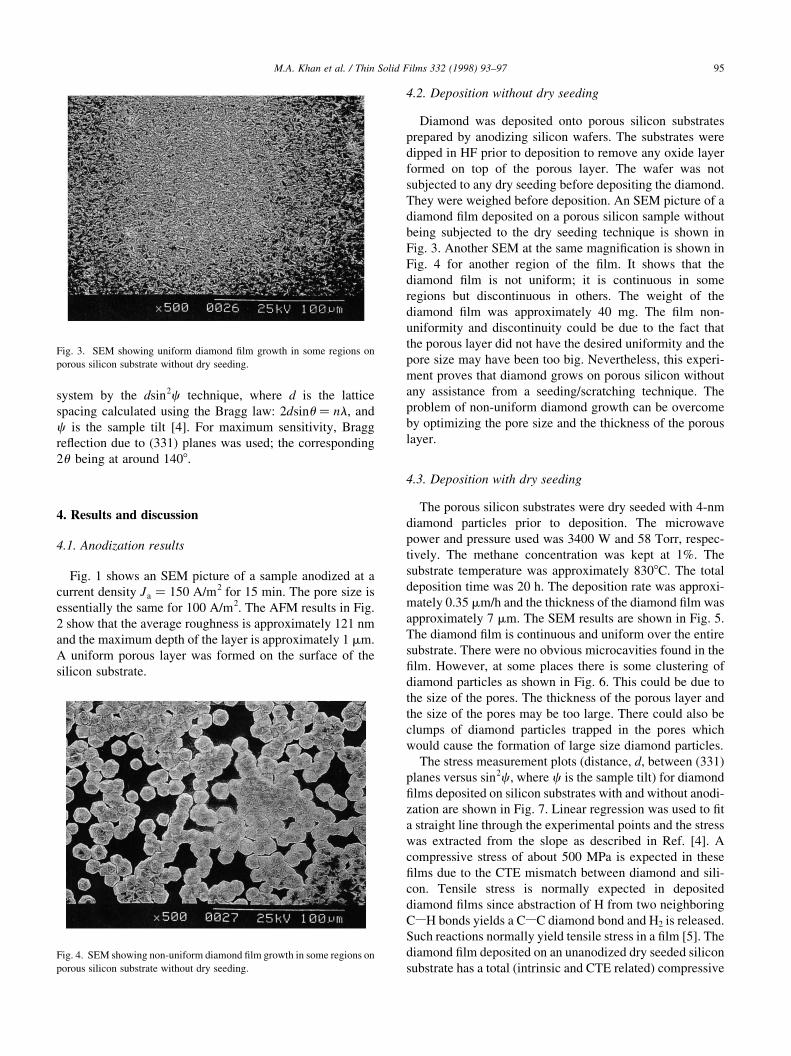
4.2. Deposition without dry seeding
Diamond was deposited onto porous silicon substrates
prepared by anodizing silicon wafers. The substrates were
dipped in HF prior to deposition to remove any oxide layer
formed on top of the porous layer. The wafer was not
subjected to any dry seeding before depositing the diamond.
They were weighed before deposition. An SEM picture of a
diamond ®lm deposited on a porous silicon sample without
being subjected to the dry seeding technique is shown in
Fig. 3. Another SEM at the same magni®cation is shown in
Fig. 4 for another region of the ®lm. It shows that the
diamond ®lm is not uniform; it is continuous in some
regions but discontinuous in others. The weight of the
diamond ®lm was approximately 40 mg. The ®lm non-
uniformity and discontinuity could be due to the fact that
the porous layer did not have the desired uniformity and the
pore size may have been too big. Nevertheless, this experi-
ment proves that diamond grows on porous silicon without
any assistance from a seeding/scratching technique. The
problem of non-uniform diamond growth can be overcome
by optimizing the pore size and the thickness of the porous
layer.
4.3. Deposition with dry seeding
The porous silicon substrates were dry seeded with 4-nm
diamond particles prior to deposition. The microwave
power and pressure used was 3400 W and 58 Torr, respec-
tively. The methane concentration was kept at 1%. The
substrate temperature was approximately 8308C. The total
deposition time was 20 h. The deposition rate was approxi-
mately 0.35 mm/h and the thickness of the diamond ®lm was
approximately 7 mm. The SEM results are shown in Fig. 5.
The diamond ®lm is continuous and uniform over the entire
substrate. There were no obvious microcavities found in the
®lm. However, at some places there is some clustering of
diamond particles as shown in Fig. 6. This could be due to
the size of the pores. The thickness of the porous layer and
the size of the pores may be too large. There could also be
clumps of diamond particles trapped in the pores which
would cause the formation of large size diamond particles.
The stress measurement plots (distance, d, between (331)
planes versus sin2c , where c is the sample tilt) for diamond
®lms deposited on silicon substrates with and without anodi-
zation are shown in Fig. 7. Linear regression was used to ®t
a straight line through the experimental points and the stress
was extracted from the slope as described in Ref. [4]. A
compressive stress of about 500 MPa is expected in these
®lms due to the CTE mismatch between diamond and sili-
con. Tensile stress is normally expected in deposited
diamond ®lms since abstraction of H from two neighboring
CZH bonds yields a CZC diamond bond and H2 is released.
Such reactions normally yield tensile stress in a ®lm [5]. The
diamond ®lm deposited on an unanodized dry seeded silicon
substrate has a total (intrinsic and CTE related) compressive
M.A. Khan et al. / Thin Solid Films 332 (1998) 93±97 95
Fig. 3. SEM showing uniform diamond ®lm growth in some regions on
porous silicon substrate without dry seeding.
Fig. 4. SEM showing non-uniform diamond ®lm growth in some regions on
porous silicon substrate without dry seeding.

stress of 140 MPa. The total compressive stress present in
the ®lm deposited on an anodized silicon substrate is 440
MPa. This means that there is a net tensile stress of 360 MPa
(after subtracting the CTE related stress component) in the
diamond ®lm deposited on an unanodized substrate,
whereas, it is only 60 MPa in the case of a porous Si
substrate. Therefore, it can be stated that porous silicon
substrates result in diamond ®lms with a signi®cantly
reduced stress. The stress reduction may be due the inter-
mediate compliant porous layer, which relieves the net
stress in the ®lm.
The adhesion of the diamond ®lm to the porous silicon
substrate was measured and was found to be 11 MPa,
whereas, the adhesion of diamond ®lm to a plain silicon
substrate is less than 7 MPa. This may be because of the
increased surface area and a better interaction between the
growing diamond and the surface silicon atoms in the case
of porous silicon. Carbon atoms may also penetrate deep
into the substrate, producing better adhesion. Hence, porous
silicon not only produces a lower stress in diamond ®lms,
but also better adhesion.
To solve the problem of clustering of diamond particles,
we changed the dry seeding procedure. Instead of dry seed-
ing the porous silicon substrate by rubbing with diamond
particles, we poured diamond powder onto the substrate and
then softly wiped the excess powder away. Thus, a porous
silicon substrate with diamond particles trapped in the pores
was obtained. Diamond was deposited on this substrate for
20 hours. A uniform ®lm was obtained without any discern-
ible large clusters on the entire surface as seen by SEM. Fig.
8 shows an SEM picture of the resulting diamond ®lm. This
is typical of the entire surface. It is clear, thus, that by
reducing the density of trapped diamond clusters in the
pores, a uniform deposited layer of diamond could be
obtained.
5. Conclusions
Diamond deposited on porous silicon without any dry
M.A. Khan et al. / Thin Solid Films 332 (1998) 93±9796
Fig. 5. SEM showing uniform diamond ®lm growth on porous silicon
substrate with dry seeding.
Fig. 6. SEM showing diamond cluster growth in some regions on porous
silicon substrate with dry seeding.
Fig. 7. Stress measurement plot (d vs. sin2c) of diamond ®lm grown on dry
seeded silicon with (solid triangles) and without (solid squares) porous Si
layer.
Fig. 8. SEM showing typical diamond morphology of ®lms deposited on
porous silicon with soft seed dispensing technique.

polishing gave non-uniform deposition and low deposition
rate. Nevertheless, it was established that nano-deformities
are potential diamond nucleation sites. Diamond ®lms
deposited on porous silicon dry seeded with 4 nm diamond
powder gave uniform nucleation and high deposition rates.
The porous silicon layer helped trap diamond nano-particles
ef®ciently to enhance the nucleation density. Thus, nano-
deformities and the diamond seed particles left on the
substrate are extremely useful for obtaining high nucleation
densities, as well a uniform growth. Porous silicon allowed
the stress in deposited diamond ®lms to be reduced consid-
erably. The adhesion of diamond ®lm to the substrate also
improved with the use of a porous silicon layer.
Acknowledgements
This research was sponsored by the Defense Advanced
Research Projects Agency (DARPA) under grant no.
MDA972-93-1-0036. The content of the information does
not necessarily re¯ect the position or the policy of the
government and no of®cial endorsement should be inferred.
References
[1] M.N. Yoder, in: K.E. Spear, J.P. Dismukes (Eds.), Synthetic Diamond,
John Wiley, New York, 1994.
[2] N. Satto, T. Yonehara, Appl. Phys. Lett. 65 (1994) 1924.
[3] H.A. Naseem, M.S. Haque, M.A. Khan, A.P. Malshe, W.D. Brown,
Thin Solid Films 308 (1997) 141.
[4] B.D. Cullity, Elements of X-Ray Diffraction, 2nd ed., Addison Wesley,
Reading, MA, 1978.
[5] M.A. Khan, Master's Thesis, University of Arkansas, 1997.
M.A. Khan et al. / Thin Solid Films 332 (1998) 93±97 97