microwave and radar - navodaya institute of technology ... · microwave and radar ... explain the...
TRANSCRIPT

Up
date
s
Dec. 2013/Jan. 2014Fifth Semester B.E. Degree Examination
Microwave and Radar
Time: 3 hrs. Max. Marks: 100
Note: 1. Answer any FIVE full questions, selecting at least two questions from each part.
PART - A
1. a. By considering elementary section of a transmission line derive transmission line equations. (08 Marks)
Ans:
v(z, t)
i(z, t)
i(z, t) z�z = (R +j�L)�z
i(z,+�z, t)
G�z C�z
i(z+�z, t)
v(z + �z, t)
�z
The change in voltage w.r.t the distance �z along the line is given by
iv Ri z L z
t
v iRi L
z t
∂Δ = Δ + Δ∂
Δ ∂∴ = +Δ ∂
v vAs z 0,
z z
Δ ∂Δ → →Δ ∂
v iRi L
z t
∂ ∂∴ = +∂ ∂ (1)
Similarly change in current w.r.t �z is given byv
i G zv C zt
i vGV C
z t
∂Δ = Δ + Δ∂
Δ ∂∴ = +Δ ∂
i iAgain as z 0,
z z
Δ ∂Δ → →Δ ∂
3-Microwave and Radar Dec 13 Jan 14.indd 343-Microwave and Radar Dec 13 Jan 14.indd 34 09/08/2014 11:32:45 AM09/08/2014 11:32:45 AM

��Microwave and Radar Dec.2013/Jan.2014
Up
date
si VGV C
z t
∂ ∂∴ = +∂ ∂
(2)
Differentiating eqn (1) w.r.t z partially, we get2
2
v i iR L
z z t z
∂ ∂ ∂ ∂⎛ ⎞= + ⎜ ⎟∂ ∂ ∂ ∂⎝ ⎠ (3)
Using (2) in (3)2
2
v v VR GV C L GV C
z t t t
∂ ∂ ∂ ∂⎡ ⎤ ⎛ ⎞= + + +⎜ ⎟⎢ ⎥ ⎝ ⎠∂ ∂ ∂ ∂⎣ ⎦
( )2 2
2 2
v v vRGV RC GL LC
z t z
∂ ∂ ∂∴ = + + +∂ ∂ ∂
(4)
∂ ∂ ∂= + + +∂ ∂ ∂
2 2
2 2
i i iSimilarly, RGi (RC GL) LCz t t
(5)
Redenote the V & I in sinusodial formV = V (z, t) = V(z) ej�t (6)i = i (z, t) = I (z) ej�t (7)differentiating eqn (6) twice w.r.t z we get
2 2j t
2 2
V d v(z)e
z dzω∂ =
∂ (8)
differentiating eqn (6) w.r.t. t we get
( )j tvv(z) e j
tω∂ = ω
∂ (9)
differentiating again w.r.t. t
( )2
2j t2
vV(z) e j
tω∂ = ω
∂
( )2
2 j t2
vv z e
tω∂∴ = −ω
∂ (10)
Using eqn (8) to eqn (10) in eqn (4) we get
( ) ( ) ( )( )2
j t j t j t 2 j t2
d V(z)e RGV(z)e RC GL V z j e LC V z e
dzω ω ω ω⎡ ⎤= + + ω + −ω⎣ ⎦
( ) ( )
( ) ( )
⎡ ⎤= + ω + − ω⎣ ⎦
= ⎡ + ω + ω + ω ⎤⎣ ⎦
22
2
d v(z) RG j RC GL LC V zdz
R G j C j L G j C V(z)
( )( )2
2
d V(z)R j L G j C V(z)
dz∴ = + ω + ω (11)
Let Z = R + j�L, Y = G + j�C (12)Z � series impedance/unit lengthy � series admittance/unit length
2
2
d V(z)ZY V(z)
dZ= (13)
3-Microwave and Radar Dec 13 Jan 14.indd 353-Microwave and Radar Dec 13 Jan 14.indd 35 09/08/2014 11:32:50 AM09/08/2014 11:32:50 AM

�� Dec.2013/Jan.2014 Microwave and Radar
Up
date
s
or 2
2
d V(z)ZY V(z) 0
dZ= = (14)
Similarly, 2
2
d I(z)ZY I(z) 0
dZ− = (15)
� Transmission line equations are
= − = −dv dIZI, YVdz dz
(16)2 2
2 22 2
d v d Iv, I
dz dz= γ = γ (17)
2where ZY ZY
ZY j
γ = ⇒ γ =
⇒ γ = = α + β
1. b. Derive an expression for the line impedance of transmission line in term of ZS and Z
O. (05 Marks)
Ans: Refer Q. no. 1a of June 2011
1. c. A load impedance of ZR = 60 –j 80� is required to be matched to a 50 ohm co - axial line, by using a
short circuited stub of length 'l' located at a distance 'd' from the load. The wavelength of operation is 1 meter. Using Smith chart, fi nd 'd' 'l'. (07 Marks)
Ans: Given data: Zl = 60 – j80� , Zo = 50�
o
Z 60 j80Z 1.2 j1.6
Z 50
−⇒ = = = − Ωl
l
Step 1: Locate Zl = 1 – 2 – j 1.6 � Smith chart and mark it as point A.
Draw line from 0 to A. With a radius of OA draw a circle and name it as constant VSWR (S) circle.Step 2: Draw a diagonally opposite line to OA and name it as B and extent it to B1. B is admittance
point.Step 3: Mark the points where S circle and G = 1 circle meets both in +ve and –ve half of Smith charts.
i.e., points C and E respectively extend C to C1 and E to E1.Step 4: When we move from admittance point in clockwise direction i.e., towards generator the first intersection point is considered i.e.,C � 1 + j1.5 with susceptance 1.5Step 5: Measure the distance from B1 to C1 i.e., d/� = 0.175 – 0.065 We know that. � = 1m (from data) �d/� = 0.11 � d = 0.11 1 m = 0.11mStep 6: Mark the susceptance of –1.5j on Smith chart as D1. Draw a line from 0 to D1. The line OD1 cuts constant S circle at D.Step 7: Measure the distance from P to D1
i.e., 0.344 0.25 0.94
0.94 1m 0.94m
= − =λ
⇒ = × ⇒ =
l
l l
3-Microwave and Radar Dec 13 Jan 14.indd 363-Microwave and Radar Dec 13 Jan 14.indd 36 09/08/2014 11:32:50 AM09/08/2014 11:32:50 AM

��Microwave and Radar Dec.2013/Jan.2014
Up
date
sZo = 50� d/� = 0.175 – 0.065 = 0.11Z
l = 60��j �� d = 0.11 � = 0.11 1 = 0.11m
o
Z 60 j80Z 1.2 1.6
Z 50
− Ω⇒ = = = − Ωl
l
Constant VSWR (S) circle
P
1/� =
0.94
Y1 = 0.3 + 10.39
B
d/� = 0.11
B1
E
E1
D1
D
A
C 1
C1+
j1.5
0.344 0.25 0.94
0.94 0.94 1m 0.94m
= − =λ
= ⇒ = × =λ
l
ll
2. a. With a near diagram, explain the working of a two hole directional coupler. Also derive the scattering matrix of the same. (10 Marks)
3-Microwave and Radar Dec 13 Jan 14.indd 373-Microwave and Radar Dec 13 Jan 14.indd 37 09/08/2014 11:32:51 AM09/08/2014 11:32:51 AM

� Dec.2013/Jan.2014 Microwave and Radar
Up
date
s
Ans:
Auxiliary waveguidePf Port (4)
Port (3)
Pb
�g
�Tiny hole 1 Tiny hole 2
PiPr
Port (1) Port (2)Main waveguide
Pt
two hole Directional compilerIn the above fig, two identical holes are drilled along the width of the main wave guide and an auxiliary wave guide.There waveguides are connected such that the holes are common between the two waveguides. The distance between three two holes is equal to �g/4 where �g is guide wavelength.Operation : There are two tiny holes 1 and 2. When the signal travels �g/4 distance, then it undergoes a phase shift of 900. Port 4 will get two signals from hole 1 and hole 2 respectively, both with a face shift of 900 . So they will add up and give forward power at port 4. port 3 will get 2 signals from holes 1 and 2 respectively but one without any phase shift, other will travel �g/4 distance to reach hole 2 and then it travels back a distance of �g/4 to reach port 3, so it has (900 + 900) = 1800 phase shift both signals out of phase by 1800 and cancelled each other, Therefore back power at port 3 is zero.S – matrix :In a directional coupler all ports are completely matched.i.e. S11 = S22 = S33 = S44 = 0 ...............(1)There is no coupling between ports 1 and port 3 and port 2 and port 4. � S13 = S31 = S24 = S42 = 0 ...............(2)
12 14
21 23
32 34
41 43
0 S 0 S
S 0 S 0S
0 S 0 S
S 0 S 0
⎡ ⎤⎢ ⎥⎢ ⎥∴ = ⎢ ⎥⎢ ⎥⎢ ⎥⎣ ⎦ ...............(3)
Equation (3) can be reduced by zero property of S matrix.* *
12 14 32 34S S S S 0+ = ...............(4)* *
21 23 41 43S S S S 0+ = ...............(5)Also from the unity property of S matrix
* *12 12 14 14S S S S 1+ = ...............(6)
Equation (4) and (5) can be written as |S12| |S14| = |S32| |S34| ..............(7)|S21| |S23| = |S41| |S43| ..............(8)Since S12 = S21, S14 = S41, S23 = S32 and S34 = S43 then|S12| = |S34| ..............(9)
3-Microwave and Radar Dec 13 Jan 14.indd 383-Microwave and Radar Dec 13 Jan 14.indd 38 09/08/2014 11:32:53 AM09/08/2014 11:32:53 AM
��Microwave and Radar Dec.2013/Jan.2014
Up
date
s|S14| = |S23| ..............(10)Let S12 = S34 = P ..............(11)Where P is +ve and real then from equation (5) ( )*
23 41P 0S S =+ ..............(12)Let 23 41S S jq= = ..............(13)Where q is +ve and real then from equation (6)p2 + q2 = 1 ..............(14)the S matrix of a direction coupler is reduced to
0 p 0 jq
p 0 jq 0S
0 jq 0 p
jq 0 p 0
⎡ ⎤⎢ ⎥⎢ ⎥=⎢ ⎥⎢ ⎥⎣ ⎦
..............(15)
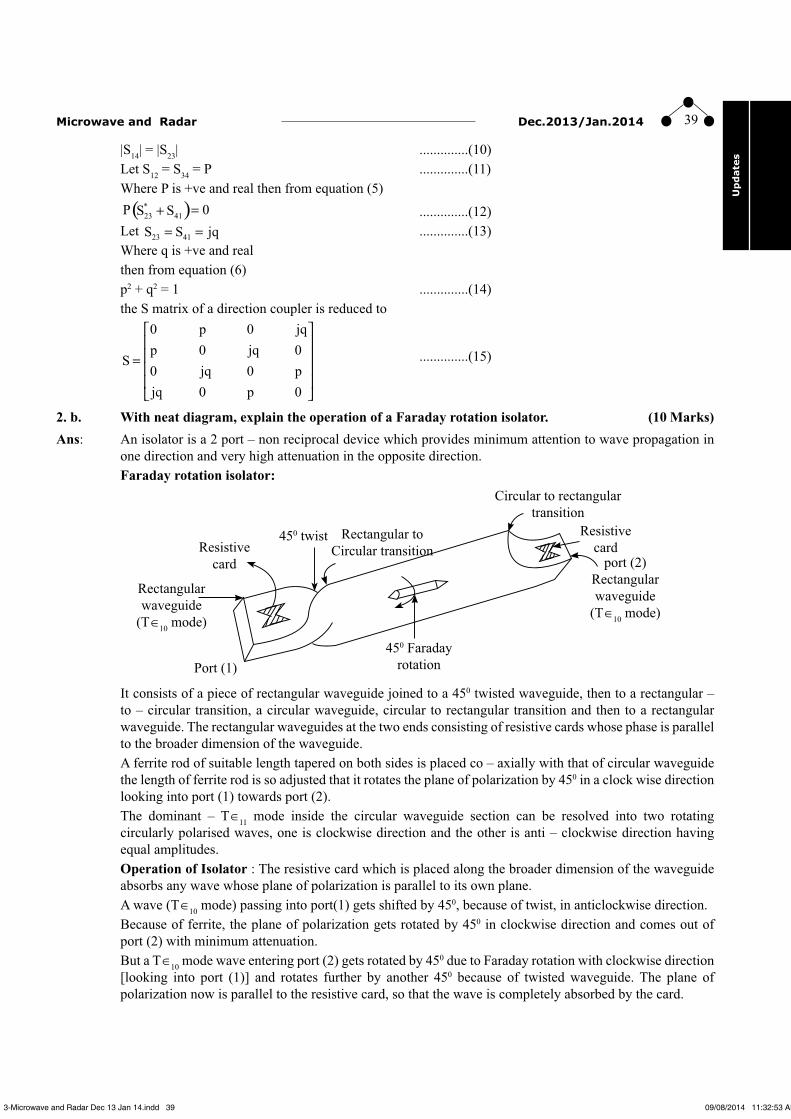
2. b. With neat diagram, explain the operation of a Faraday rotation isolator. (10 Marks)
Ans: An isolator is a 2 port – non reciprocal device which provides minimum attention to wave propagation in one direction and very high attenuation in the opposite direction.Faraday rotation isolator:
450 Faraday rotation
Circular to rectangular transition
Resistive card
port (2) Rectangular waveguide
(T�10 mode)
Rectangular toCircular transition
450 twistResistive
card
Rectangular waveguide
(T�10 mode)
Port (1)
It consists of a piece of rectangular waveguide joined to a 450 twisted waveguide, then to a rectangular – to – circular transition, a circular waveguide, circular to rectangular transition and then to a rectangular waveguide. The rectangular waveguides at the two ends consisting of resistive cards whose phase is parallel to the broader dimension of the waveguide.A ferrite rod of suitable length tapered on both sides is placed co – axially with that of circular waveguide the length of ferrite rod is so adjusted that it rotates the plane of polarization by 450 in a clock wise direction looking into port (1) towards port (2).The dominant – T�11 mode inside the circular waveguide section can be resolved into two rotating circularly polarised waves, one is clockwise direction and the other is anti – clockwise direction having equal amplitudes.Operation of Isolator : The resistive card which is placed along the broader dimension of the waveguide absorbs any wave whose plane of polarization is parallel to its own plane.A wave (T�10 mode) passing into port(1) gets shifted by 450, because of twist, in anticlockwise direction. Because of ferrite, the plane of polarization gets rotated by 450 in clockwise direction and comes out ofport (2) with minimum attenuation.But a T�10 mode wave entering port (2) gets rotated by 450 due to Faraday rotation with clockwise direction [looking into port (1)] and rotates further by another 450 because of twisted waveguide. The plane of polarization now is parallel to the resistive card, so that the wave is completely absorbed by the card.
3-Microwave and Radar Dec 13 Jan 14.indd 393-Microwave and Radar Dec 13 Jan 14.indd 39 09/08/2014 11:32:53 AM09/08/2014 11:32:53 AM

�� Dec.2013/Jan.2014 Microwave and Radar
Up
date
s
3. a. What is 'Gunn Effect'? With a neat diagram explain the constructional details of a Gunn diode. (08 Marks)
Ans: Gunn effect:
From Gunn's observation the carrier drift velocity is linearly increased from zero to a maximum when electric � eld is varied from zero to a threshold value (3000V/cm for n type GaAs), when E � eld is beyond the threshold value then the drift velocity decreased and the diode exhibits Negative resistance as shown in � gure. This is called Gunn effect.
0 3 4Field kV/cm
Drift velocity
cm/s
2 107
107
5 10 15 20
Construction of details of Gunn diode:
––
––––––
– +– +– +– +– +––– +
+++++
+Anode
High � eld domain
Cathode
Metal coated contact
+++ Metal (Au) stud cathode
n+ layer
n+ substrate
Metal (Au) anode contact
Active n - layer (10�m for 10GHz)
A Gunn diode consists of n - type GaAs semiconductor with regions of high doping (n+). Although there is no junction, this is called a diode with reference to the +ve end (anode) and –ve end (cathode) of the dc voltage applied across the device.If voltage or electric field at low level is applied to the GaAs initially the current will increase with a rise in the voltage. When a diode voltage exceeds certain threshold voltage a high electric field (3.2 kV/m for GaAs) produced across the active region and electrons are excited from their initial lower valley to the higher valley, where they become virtually immobile.If the rate at which electrons are transferred is very high, the current will decrease with increase in voltage resulting in the equivalent negative resistance effect.Since GaAs is not a good conductor, considerable heat is generated within the diode. The diode should be well bounded into a heat sink (Cu - stud).The equivalent circuit of Gunn diode is as shown below.
Cj
CP
–Rj
LP
RS
[Equivalent circuit of Gunn diode]
3-Microwave and Radar Dec 13 Jan 14.indd 403-Microwave and Radar Dec 13 Jan 14.indd 40 09/08/2014 11:32:53 AM09/08/2014 11:32:53 AM

��Microwave and Radar Dec.2013/Jan.2014
Up
date
sCj and Rj � are diode capacitance and resistance.RS � includes total resistance of lead, ohmic contact and bulk resistance of diode.CP � Package capacitanceLP � Package InductanceThe value of negative resistance is –5� to –20�
3. b. Give a brief account of RWH theory. (06 Marks)
Ans: RWH (Ridley - Watkins - Hilsum) theory consists two concepts
i) Differential negative resistance
ii) Two valley theory
i) Differential negative resistance: The fundamental concept of RWH theory is differential negative resistance developed in a bulk solid state compound when either a voltage or a current is applied to the terminals of the sample.
There are two modes of negative resistance devices voltage controlled mode and current controlled mode.
J
E E
J
Negative resistance region
Negative resistance region
Voltage controlled mode Current controlled mode
High � eld
Low � eld
I I
Low current
High current
High field domain High field filament(Voltage controlled mode) (Current controlled mode)
In voltage controlled, the current density is multivalued and in current controlled, the voltage can be �multivalued.Due to negative resistance region in current density curve the sample leads to be unstable, as a result �the initially, homogeneous sample becomes heterogeneous to reach stability.In voltage controlled mode high � eld domains are formed by separating two low � eld regions, where �as in current controlled mode, High current � lament will be running along the � eld direction.
dI dJNegative resis tan ce
dV dE= =
ii. Two valley theory:
3-Microwave and Radar Dec 13 Jan 14.indd 413-Microwave and Radar Dec 13 Jan 14.indd 41 09/08/2014 11:32:53 AM09/08/2014 11:32:53 AM

�� Dec.2013/Jan.2014 Microwave and Radar
Up
date
s
According to the energy bond theory of the n type GaAs, a high mobility lower valley is separated by an energy of 0.36eV from a low - mobility upper valley as shown below.
Eg = 1.43ev
Lower valley
Upper valley
�E = 0.36ev
Conduction band
Forbidden band
Valence bandK
When applied field is lower than the E field of the lower valley (E < El) no electrons will transfer from
lower to upper valley
E
K
E
K
E
K a) E < E
l b) E
l < E < Eu c) E > Eu (or) Eu < E
When the applied � eld is higher than that of lower valley and than that of upper valley (E �l< E < Eu)
electrons will begin to transfer to the upper valley.When applied � eld is greater than that of upper valley i.e., (E > E � u) all the electrons transfer to the upper valley.
3. c. With neat diagram, explain the construction and operation of Schottky barrier diode. (06 Marks)
Ans: Schottky Barrier diode : It is a point contact – silicon crystal diode, where the metal – semiconductor function formed is a surface rather than a point contact. It dominates the minority carrier flow in the reverse biased condition of the diode.
n
Rectifying surface constantGold or
aluminium
SiO2
Gold or Aluminium
n+ substrate
CC
LS
RS
CjRj
(a) Schottky barrier diode (b) Equivalent CircuitThe diode consists of n+ silicon substrate upon which a thin layer of silicon of 2 to 3 micron thickness
3-Microwave and Radar Dec 13 Jan 14.indd 423-Microwave and Radar Dec 13 Jan 14.indd 42 09/08/2014 11:32:53 AM09/08/2014 11:32:53 AM

��Microwave and Radar Dec.2013/Jan.2014
Up
date
sis epitaxially grown. Then a thin insulating layer of silicon dioxide is grown thermally. After opening a window through masking process, a metal – semiconductor function is formed by depositing metal over Sio2.Because of larger contacts area of rectifying contact, the forward resistance is lower as also noise.
4. a. Explain S - matrix representation of multiport network. (07 Marks)
Ans: S-parameters for 2 port network
Zg Zo
Z S
Zo
OutputInput
ZLa1
b1
Pi
Pi-Pr
PrPo
Device 2 port network ZVg
The incident & re� ected amplitudes of microwaves at any port are used to characterise a microwave circuit.The amplitudes of these are normalised.
2thin n
1Input power at n port P = a
2⇒ (1)
2thr n n
1Reflected power at n port P = b
2⇒ (2)
an � Normalised incident wave amplitude at nth port bn � Normalised re� ected wave amplitude at nth portFor a two port network, the relation between incident & re� ected waves are expressed in terms of S-parameters Sij b1 = S11 a1 + S12 a2 (3)b2 = S21 a1 + S22 a2 (4)S11 = b1/a1|a2
= 0
� Re� ection coef� cient K1 at port 1 when port 2 is terminated with matched load (a2 = 0)
S22 = b2/a2|a1 = 0
� Re� ection coef� cient K2 at port 2 when port 1 is terminated with matched load (a1 = 0)
S12 = b1/a2|a1 = 0
� Attenuation of wave travelling from port 2 to port 1S21 = b2/a1|a2
= 0
� Attenuation of wave travelling from port 1 to port 2
In general [b] = [s] [a]
11 12 1N1 1
21 22 2N2 2
N NN1 N2 NN
S S ............Sb a
S S ............Sb a
b aS S ...........S
⎡ ⎤⎡ ⎤ ⎡ ⎤⎢ ⎥⎢ ⎥ ⎢ ⎥⎢ ⎥⎢ ⎥ ⎢ ⎥
⇒ = ⎢ ⎥⎢ ⎥ ⎢ ⎥⎢ ⎥⎢ ⎥ ⎢ ⎥⎢ ⎥⎢ ⎥ ⎢ ⎥
⎣ ⎦ ⎣ ⎦⎣ ⎦
4. b. Explain symmetrical Z and Y matrix for reciprocal network. (08 Marks)
Ans: In reciprocal network, the impedance and the admittance matrices are symmetrical and the junction �
3-Microwave and Radar Dec 13 Jan 14.indd 433-Microwave and Radar Dec 13 Jan 14.indd 43 09/08/2014 11:32:53 AM09/08/2014 11:32:53 AM

�� Dec.2013/Jan.2014 Microwave and Radar
Up
date
s
media is characterized by scalar electrical parameters permittivity (�) permeability (�).For multiport network (N ports), let the incident wave amplitude V � n
+ be so chosen that the total voltage.
Vn = Vn+ + V–
n at all ports n = 1, 2, ............ N, except the ith port where the fields are Ei, Hi. Similarly let Vn = 0 at all ports except jth port where fields are Ei, Hi. Then from Lorentz reciprocity theorem.
( )i j j i
S
E H E H .ds 0× − × =∫ (1)where S is closed surface area of the conducting walls enclosing junction and N ports in absence of any source.Since the integral over the perfectly conducting walls vanishes, the only non - zero integrals are those taken over the reference planes of the corresponding ports, so that.
( )n
N
i j j in 1 t
E H E H .ds 0=
× − × =∑∫ (2)
Since Vn except Vi and Vj are zero,Eti = n Ei and Etj = n Ej are zero on all reference planes at the corresponding ports ti and tj respectively.� Eqn (2) reduces to
( ) ( )i j
i j j i
t t
E H .dS E H ds× = ×∫ ∫ (3)
OR Pij = Pji (4)Where Pij represents the power at reference plane i due to an input voltage at plane j.From admittance matrix representation [I] = [Y] [V] and power relation P = VIEqn (4) reduces toViVj Yij = Vj Vi Yji OR Yij = Yji (5) Zij = Zji (6)This proves that impedance and admittance matrices are symmetrical for a reciprocal Junction.
4. c. Explain symmetric properties of S - matrix. (05 Marks)
Ans: If a microwave junction satis� es reciprocity condition and if these are no active devices, then the S - parameters are equal to their corresponding transposes.i.e., Sij = Sji (i � j)which results [S]t = [S]Proof:
( )
( )
n
i ij ij jj 1
n
i ij ij jj 1
1a Z I and
2
1b Z I
2
=
=
= + δ
= − δ
∑
∑
where �ij � "Kronecker delta".
ij
ij
1 if i j
0 if i j
δ = =⎧⎪⎨δ = ≠⎪⎩
In matrix notation
[ ] [ ] [ ]{ }[ ] ( )
[ ] [ ] [ ]{ }[ ] ( )
1a Z U I 1
21
b Z U I 22
= +
= − where [U] � Identify matrix
So, {[Z] + [U]} [I] = 2[a]
3-Microwave and Radar Dec 13 Jan 14.indd 443-Microwave and Radar Dec 13 Jan 14.indd 44 09/08/2014 11:32:54 AM09/08/2014 11:32:54 AM
��Microwave and Radar Dec.2013/Jan.2014
Up
date
sPremultiplying both sides by {[Z] + [U]}–1 we get{[Z] + [U]} {[Z] + [U]}–1 [I] = 2{[Z] + [U]–1 [a]� {[I] = 2{[Z] + (U)}–1 [a]Substitute above equation in (2)� [b] = {[Z] – [U]} {[Z] + [U]–1} [a] (3)We know that, [b] = [s] [a] (4)Compare eqns (3) and (4) we get[S] = {[Z] – [U]} {[Z] + [U]}–1 (5)Let P = [Z] – [U] Q= [Z] + [U]Now eqn (5) becomes[S] = [P] [Q]–1 (6)For a reciprocal network, the [Z] matrix is symmetricHence [P] and [Q] are also symmetric so that,[P] [Q] = [Q] [P] (7)Pre and post multiply equation (7) on both side by Q–1
[Q]–1 [P] [Q] [Q]–1 = [Q]–1 [Q] [P] [Q]–1
� [Q]–1 P = [P] [Q]–1 = [S] (8)Consider now the transpose of [S] i.e., eqn (5)
[ ] [ ]{ } [ ] [ ]{ } ( )[ ] [ ]{ } [ ] [ ]{ } ( )
1 1
T
T
Z U Z U 10
& Z U Z U 11
− −+ = +
− = +
Using equations (10) and (11) in (9)
[ ] [ ] [ ]{ } [ ] [ ]{ }[ ] [ ] ( )
1
T
1
T
S Z U Z U
S Q P 12
−
−
= + −
=
Compare equations (6) and (12) we get [S] = [S]T
PART - B
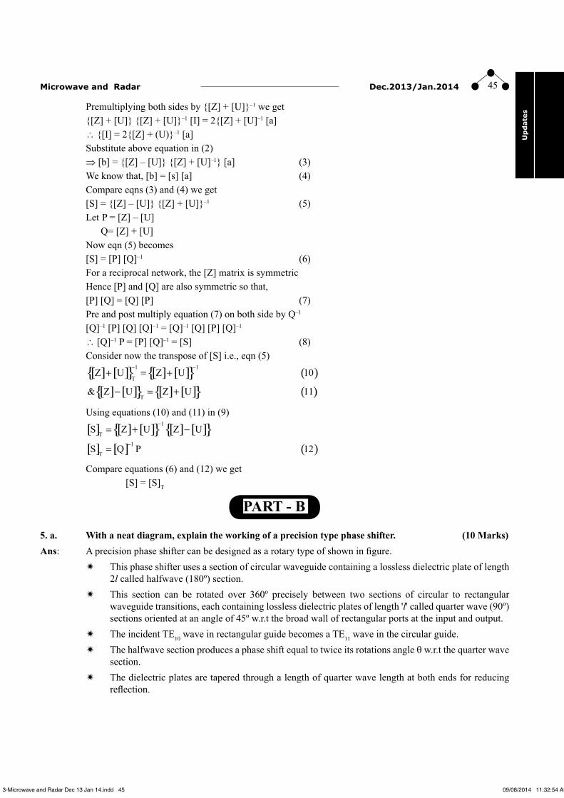
5. a. With a neat diagram, explain the working of a precision type phase shifter. (10 Marks)
Ans: A precision phase shifter can be designed as a rotary type of shown in � gure.This phase shifter uses a section of circular waveguide containing a lossless dielectric plate of length �2l called halfwave (180º) section.This section can be rotated over 360º precisely between two sections of circular to rectangular �waveguide transitions, each containing lossless dielectric plates of length 'l' called quarter wave (90º) sections oriented at an angle of 45º w.r.t the broad wall of rectangular ports at the input and output.The incident TE � 10 wave in rectangular guide becomes a TE11 wave in the circular guide.The halfwave section produces a phase shift equal to twice its rotations angle � � w.r.t the quarter wave section.The dielectric plates are tapered through a length of quarter wave length at both ends for reducing �re� ection.
3-Microwave and Radar Dec 13 Jan 14.indd 453-Microwave and Radar Dec 13 Jan 14.indd 45 09/08/2014 11:32:54 AM09/08/2014 11:32:54 AM

�� Dec.2013/Jan.2014 Microwave and Radar
Up
date
s
Ei
y z
Dielectric plates
x
4π plate
Plane of input plate
Rotary section
�/2 plate�/4 plate
Ei <2�
Plane of rotary plate
E2Y
E1
Ei
450
X
E4Y E5
E3
450
X
E4E2 E6
Y
��
E1
E3
X
Input 4π plate Rotary
2
π plate Output 4π plate
Principle of operation:
The TE � 11 mode incident � eld Ei in the input quarter wave section can be decomposed into two transverse components.
One E1 polarised parallel and other E2 perpendicular to quarter wave plate. After propagation through the quarter wave plate these components areE1 = Ei cos 45º e–j��l = E0 e
–j��l (1)E2 = Ei sin 45º e–j��l = E0 e
–j��l (2)
i0
Ewhere E2
=
The length 'l' is adjusted such that there 2 components will have equal magnitude but a differential phase angle of (�1 – �2)l = 900
� After propagation through quarter wave plate field components become( )
( )
1
1
j1 0
jj 2
2 0 1 1
E E e 3
E jE e jE E e 4
− β
π− β
=
= = =
l
l
3-Microwave and Radar Dec 13 Jan 14.indd 463-Microwave and Radar Dec 13 Jan 14.indd 46 09/08/2014 11:32:54 AM09/08/2014 11:32:54 AM

��Microwave and Radar Dec.2013/Jan.2014
Up
date
sThus 4π section convert linearly polarized TE11 wave to circularly polarised wave and vice - versa.
After emergence from the halfwave section, the field components parallel and perpendicular to the halfwave plate isE3 = (E1 cos � – E2 sin �) ( )2 1j2 j3j
0e E e e 5− β − β− θ=l l
E4 = (E2 cos � + E1 sin �) ( )2 1jj2 j3j 2
0e E e e e 6π−− β − β− θ=l l
( ) ( )1 2 2 12 or 2 2 7β −β = π − β = π − βl l l
Then the � eld components E � 3 and E4 may again be decomposed into two TE11 modes, polarised parallel and perpendicular to the output quarterwave plate.At the output end of quarterwave plate the � eld components parallel and perpendicular to the quarter �wave plate is( ) ( )( ) ( )
1 1
2 1
j j4j25 3 4 0
j j4j26 4 3 0
E E cos E sin e E e e 8
E E cos E sin e E e e 9
− β − β− θ
− β − β− θ
= θ + θ =
= θ − θ =
l l
l l
The resultant field i.e., linearly polarised TE11 wave
( )1 1j4 j4j2 j2out 0 iE 2E e e E e e 10− β − β− θ − θ= =l l
5. b. With a neat diagram, explain the working of a H - plane Tee Junction. Also derive its scattering matrix. (10 Marks)
Ans: In an H - plane Tee, if two in - phase input waves are fed into port1 and port 2 of the collinear arm, the output waves at port 3 will be in phase and additive. of this the third port is called the sum arm.OR an input wave at port 3 will be equally divided into ports 1 and 2 in phase.Because the magnetic field loops get divided into two arms 1 and 2 in a manner perpendicular to currents between branches in the parallel circuit.
Plane of symmetry
Port 1
Port 2
Port 3
Side arm
(H arm)
S - matrix derivation:
i. Because of Symmetry input at port 3 divided into 1 and 2 collinear arms.
� S31 = S32
ii. Port 3 is perfectly matched.
S33 = 0
3-Microwave and Radar Dec 13 Jan 14.indd 473-Microwave and Radar Dec 13 Jan 14.indd 47 09/08/2014 11:32:54 AM09/08/2014 11:32:54 AM

� Dec.2013/Jan.2014 Microwave and Radar
Up
date
s
iii. From The symmetry property
Sij = Sji
[ ]11 12 13
21 22 23H
31 32 33
S S S
We know that S S S S
S S S
⎡ ⎤⎢ ⎥= ⎢ ⎥⎢ ⎥⎣ ⎦
Use above 3 properties in (*) matrix
[ ]11 12 13
12 22 13H
13 13
S S S
S S S S
S S 0
⎡ ⎤⎢ ⎥∴ = ⎢ ⎥⎢ ⎥⎣ ⎦
Since S21 = S12, S23 = S32 = S31 = S13
iv. From unitary property [S] [S] * = [U]
* * *1 1 1 2 1311 12 13
* * *12 22 13 1 2 22 13
* *13 13 1 3 13
S S SS S S 1 0 0
S S S S S S 0 1 0
0 0 1S S 0 S S 0
⎡ ⎤⎡ ⎤ ⎡ ⎤⎢ ⎥⎢ ⎥ ⎢ ⎥⇒ =⎢ ⎥⎢ ⎥ ⎢ ⎥⎢ ⎥⎢ ⎥ ⎢ ⎥⎣ ⎦⎣ ⎦ ⎣ ⎦
Multiply 1st row of 1st matrix and 1st column of 2nd matrix
S11 S11* + S12 S
*12 + S13 S
*13 = 1
� |S11|2 + |S22|
2 + |S13|2 = 1 (1)
Multiply 2nd row of 1st matrix and 2nd column of 2nd matrix
S12S12* + S22S22
* + S13S13* = 1
� |S12|2 + |S22|
2 + |S13|2 = 1 (2)
Multiply 3rd of 1st matrix and 3rd column of 2nd matrix
S13 S13* + S13 S
*13 + 0 = 1
� |S13|2 + |S13|
2 = 1
� 2|S13|2 = 1 (3)
Multiply 3rd row of 1st matrix and 1st column of 2nd matrix
S13 S11* + S13 S
*12 = 0 (4)
From eqn (3) � 2|S31|2 = 1 13
1S
2⇒ = (5)
S11 = S22 (6)
From eqn (4) S13 (S*11 + S*
12) = 0
Since S13�0, S*12S
*11 = 0 � S*
12 = –S*11 � S12 –S11 (7)
Using eqn (7) and (5) in eqn (1)
|S11|2 + |S12|
2 + 2
1
2
⎛ ⎞⎜ ⎟⎝ ⎠
= 1
� |S11|2 + |S11|
2 + 2
1
2
⎛ ⎞⎜ ⎟⎝ ⎠
= 1
3-Microwave and Radar Dec 13 Jan 14.indd 483-Microwave and Radar Dec 13 Jan 14.indd 48 09/08/2014 11:32:55 AM09/08/2014 11:32:55 AM

��Microwave and Radar Dec.2013/Jan.2014
Up
date
s211
11
1 12 | S | 1
2 21S 2
⇒ = − =
⇒ =
12 11
22 11
1S S
21
S S2
∴ = − = −
= =
[ ]H
1 1 1
2 2 21 1 1S 2 2 21 1 0
2 2
⎡ ⎤−⎢ ⎥⎢ ⎥−⎢ ⎥∴ =⎢ ⎥⎢ ⎥⎢ ⎥⎣ ⎦
[ ]1 1 1 1
2 2 2 2H
3 3 3 3
1 1 1
2 2 2b a b a1 1 1We know that b S a b a2 2 2
b a b a1 1 0
2 2
⎡ ⎤−⎢ ⎥⎡ ⎤ ⎡ ⎤ ⎡ ⎤ ⎡ ⎤⎢ ⎥⎢ ⎥ ⎢ ⎥ ⎢ ⎥ ⎢ ⎥−⎢ ⎥= ⇒ =⎢ ⎥ ⎢ ⎥ ⎢ ⎥ ⎢ ⎥⎢ ⎥⎢ ⎥ ⎢ ⎥ ⎢ ⎥ ⎢ ⎥⎢ ⎥⎣ ⎦ ⎣ ⎦ ⎣ ⎦ ⎣ ⎦⎢ ⎥⎣ ⎦
1 1 2 3
2 1 2 3
3 1 2
1 1 1b a a a
2 2 21 1 1
b a a a2 2 21 1
b a a 02 2
⇒ = − +
−= + +
= + +
6. a. Calculate the characteristic impedance of a wide microstrip line having negligible thickness and having a width at 0.8 mm, thickness at substrate 0.2mm and has a dielectric constant 3.55.
(04 Marks)
Ans: Given data:Zo = ? W = 0.8mm, h = 0.2 mm, �r = 3.55W >> h,
o
r
o
o
377 hZ
w
377 0.2Z
0.83.55
Z 50
⎛ ⎞= ⎜ ⎟ε ⎝ ⎠
⎛ ⎞⇒ ⎜ ⎟⎝ ⎠⇒ = Ω
6. b. Explain the various losses taking place in microstrip lines. (08 Marks)
Ans: When the dielectric substrate of dielectric constant �r is purely non – magnetic then there are 3 types of losses in microstripline .a. Dielectric losses in the substrateb. Ohmic losses in the strip and ground plane c. Radiation losses
3-Microwave and Radar Dec 13 Jan 14.indd 493-Microwave and Radar Dec 13 Jan 14.indd 49 09/08/2014 11:32:55 AM09/08/2014 11:32:55 AM
�� Dec.2013/Jan.2014 Microwave and Radar
Up
date
s
a. Dielectric losses : All dielectric materials possess some conductivity � but it will be small that � < w� when this � is not negligible, the electric and magnetic � elds in the dielectric are no longer in time phase.
In that case the dielectric attenuation constant, and expressed as
d Np / cm2
σ μα = ε .............(1)
Loss tangent is tanw
σθ =ε
.............(2)
The dielectric attenuation constant is
d
wtan Np / cm
2α = με θ .............(3)
b. Ohmic losses: In MSL major contribution to the losses at microwave frequency is from the � nite � of microstrip conductor placed on a low loss dielectric substrate.
Due to the current flowing through the conductor there will be ohmic loss and hence attenuation of signal twice place.
Attenuation constant due to ohmic loss of a wide MSL w1
h⎡ ⎤>⎢ ⎥⎣ ⎦
is c
c0
8.686RdB / cm
Z Wα −
Where S
fR
π μ= →σ
surface skin resistance in �/cm2
c. Radiation losses: At microwave frequencies the microstrip line acts as an antenna radiating small amount of power, resulting in radiation losses.
The radiation loss depends on the substrate's thickness and dielectric constant, as well as its geometry.The ratio of radiated power Prad to the total dissipated power Pt for an open microstrip is given by
rad r
t r
P R
P Z= ............(1)
Z0 � Characteristic impedance Rr � Radiation resistance
6. c. With a neat diagram, explain shielded strip lines. (08 Marks)
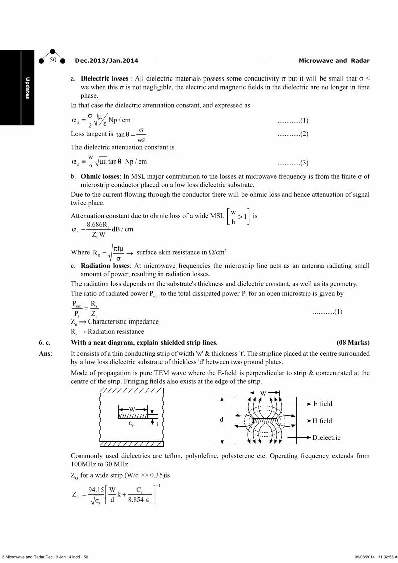
Ans: It consists of a thin conducting strip of width 'w' & thickness 't'. The stripline placed at the centre surrounded by a low loss dielectric substrate of thickless 'd' between two ground plates.Mode of propagation is pure TEM wave where the E-� eld is perpendicular to strip & concentrated at the centre of the strip. Fringing � elds also exists at the edge of the strip.
W
t�rd
WE � eld
H � eld
Dielectric
Commonly used dielectrics are te� on, polyole� ne, polysterene etc. Operating frequency extends from 100MHz to 30 MHz.ZO for a wide strip (W/d >> 0.35)is
1
fO
rr
C94.15 WZ k
d 8.854
−⎡ ⎤
= +⎢ ⎥∈∈ ⎣ ⎦
3-Microwave and Radar Dec 13 Jan 14.indd 503-Microwave and Radar Dec 13 Jan 14.indd 50 09/08/2014 11:32:55 AM09/08/2014 11:32:55 AM

��Microwave and Radar Dec.2013/Jan.2014
Up
date
s1where K
t1 d
=−
t � the strip thickness d � the distance between two ground plates.
( ) ( ) ( )2rf
8.854C 2k ln k 1 k 1 ln k 1
Fringe capacitance in pF / m
∈ ⎡ ⎤= + − − −⎣ ⎦π
7. a. Derive radar range equation in terms of effective aperture, radar cross section of target and minimum detectable signal power of receiver. (10 Marks)
Ans: Radar equation relates the range of the radar to characteristics of the transmitter, receiver, antenna, target & environment.If the transmitter power Pt is radiated by an isotropic antenna.The power density at a distance R from the radar is equal to radiated power divided by the surface area.
t2
PPower densityat range R is W/sq.m
4 R∴
π (1)
But Radar employ directive antenna to concentrate the radiated power Pt in a particular direction.
t2
P GPower density at range R from directive antenna is
4 R∴
π (2)
Wheremax power density radiated by directive antenna
GPower density radiated by lossless isotropicantenna
=
The target intercepts a portion of incident energy and reradiates in various directions.The radar cross section of the target determines the power density returned to the radar.
t2 2
P GReradiated power density back at the radar
4 R 4 R
σ∴ =π π
(3)
The radar antenna captures a portion of the incident eacho signal.The power received by the radar = incident power × effective area
tr e2 2
P GP A
4 R 4 R
σ=π π
(4)
where Ae = �a A. [A: physical area, �a: Antenna aperture ef� ciency]The maximum range of radar Rmax is the distance beyond which target cannot be detected.� Pr is equal to minimum detectable signal Smin
t er min 2 2
P G .AP S
4 R 4 R
σ∴ = =
π π
( )
14
t emax 2
min
P GAR
4 S
⎡ ⎤σ∴ = ⎢ ⎥
π⎢ ⎥⎣ ⎦ (5)
e2
4 A cBut WKT, G , wavelength fπ
= λ → =λ
3-Microwave and Radar Dec 13 Jan 14.indd 513-Microwave and Radar Dec 13 Jan 14.indd 51 09/08/2014 11:32:55 AM09/08/2014 11:32:55 AM

�� Dec.2013/Jan.2014 Microwave and Radar
Up
date
s ( )
142 2
tmax 3
min
P GR
4 S
⎡ ⎤λ σ∴ = ⎢ ⎥
π⎢ ⎥⎣ ⎦ (6)
OR1
2 4t e
max 2min
P AR
4 S
⎡ ⎤σ= ⎢ ⎥πλ⎣ ⎦
(7)
7. b. Discuss various applications of radar. (05 Marks)
Ans: Various applications of Radar: Radar has been employed to detect targets on the ground, on the sea, in the air, in space & even below ground.Major areas of Radar applications are 1. Military: Radar is an important part of air-defence systems
It will be used for surveillance & weapon control. Surveillance includes target detection, target �recognition, target tracking & designation to a weapon system.Weapon control radars track targets, detect the weapon to an intercept �High resolution radars such as SAR are used for detecting � xed & moving targets on the �battle� eld.
2. Remote sensing: All radars are remote sensors. Ex:
a) Weather observation, which is a regular part of TV weather reporting, done by Radar remote sensing
b) Planetary observationc) Short-range below ground probingd) Mapping of sea ice to route shipping
3. Air traffi c Control: In the vicinity of airports radars have been employed for safety control of air traf� c.
To enroute aircraft from one airport to another ASR (Air survivalnce radars) will be employed �ASR also maps regions of rain so that aircraft can be directed around them �TDWR (Terminal Doppler weather radars) are dedicatedly employed for observing weather in �the vicinity of airports.
4. Law enforcement & highway safety:A radar speed meter is used by police to measure the speed of vehicles �Radars are used to measure the speed of tennis ball �
5. Aircraft safety & Navigation:Some radars outline the regions of dangerous wind shear to allow the pilot to avoid hazardous �conditionsTo measure the height of radar from earth, radar altimeter will be used �
6. Ship Safety: Radar is found on ships & boats for collision avoidance & to enroute the slip when visibility is poor
7. Space: Space vehicles use radars for landing on moon. Large ground based radars are used for detection & tracking of satellites and other space objects.
8. Other applications:In industry for measurement of speed & distance �
3-Microwave and Radar Dec 13 Jan 14.indd 523-Microwave and Radar Dec 13 Jan 14.indd 52 09/08/2014 11:32:55 AM09/08/2014 11:32:55 AM
��Microwave and Radar Dec.2013/Jan.2014
Up
date
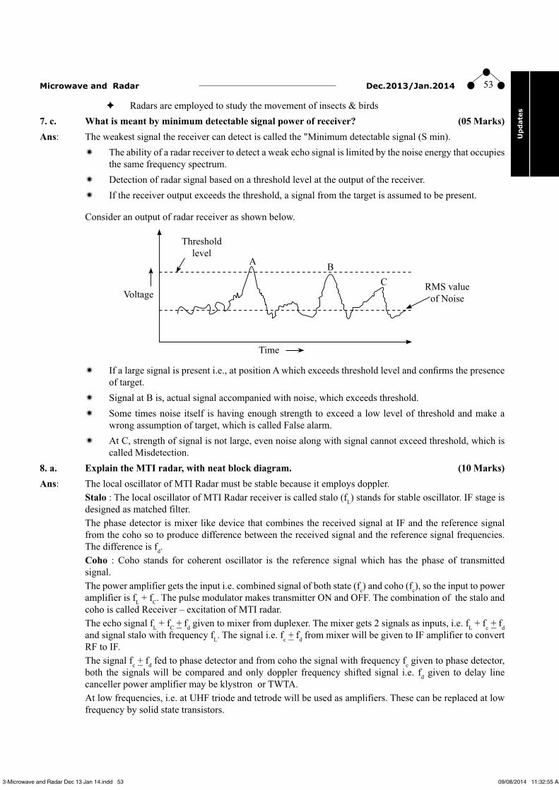
sRadars are employed to study the movement of insects & birds �7. c. What is meant by minimum detectable signal power of receiver? (05 Marks)
Ans: The weakest signal the receiver can detect is called the "Minimum detectable signal (S min).The ability of a radar receiver to detect a weak echo signal is limited by the noise energy that occupies �the same frequency spectrum.Detection of radar signal based on a threshold level at the output of the receiver. �If the receiver output exceeds the threshold, a signal from the target is assumed to be present. �
Consider an output of radar receiver as shown below.
RMS value of Noise
Threshold level
Voltage
Time
A BC
If a large signal is present i.e., at position A which exceeds threshold level and con� rms the presence �of target.Signal at B is, actual signal accompanied with noise, which exceeds threshold. �Some times noise itself is having enough strength to exceed a low level of threshold and make a �wrong assumption of target, which is called False alarm.At C, strength of signal is not large, even noise along with signal cannot exceed threshold, which is �called Misdetection.
8. a. Explain the MTI radar, with neat block diagram. (10 Marks)
Ans: The local oscillator of MTI Radar must be stable because it employs doppler.Stalo : The local oscillator of MTI Radar receiver is called stalo (fL) stands for stable oscillator. IF stage is designed as matched filter.The phase detector is mixer like device that combines the received signal at IF and the reference signal from the coho so to produce difference between the received signal and the reference signal frequencies. The difference is fd. Coho : Coho stands for coherent oscillator is the reference signal which has the phase of transmitted signal.The power amplifier gets the input i.e. combined signal of both state (fc) and coho (fc), so the input to power amplifier is fL + fC. The pulse modulator makes transmitter ON and OFF. The combination of the stalo and coho is called Receiver – excitation of MTI radar.The echo signal fL + fC +_ fd given to mixer from duplexer. The mixer gets 2 signals as inputs, i.e. fL + fc +_ fd and signal stalo with frequency fL. The signal i.e. fc +_ fd from mixer will be given to IF amplifier to convert RF to IF.The signal fc +_ fd fed to phase detector and from coho the signal with frequency fc given to phase detector, both the signals will be compared and only doppler frequency shifted signal i.e. fd given to delay line canceller power amplifier may be klystron or TWTA.At low frequencies, i.e. at UHF triode and tetrode will be used as amplifiers. These can be replaced at low frequency by solid state transistors.
3-Microwave and Radar Dec 13 Jan 14.indd 533-Microwave and Radar Dec 13 Jan 14.indd 53 09/08/2014 11:32:55 AM09/08/2014 11:32:55 AM

�� Dec.2013/Jan.2014 Microwave and Radar
Up
date
s
Pulse modulator
Duplexer Power ampli� er
Mix MixStalo
FL
IFampli� er
Phasedetector
Cohofc
Reference signal
fd
To DLC
fL + Fc +_ fd
fc +_ fd
fL + fC
fL + fC
MTI Block diagram
8. b. With neat block diagram, explain moving target detector. (05 Marks)
Ans:
3 Pulse canceler
Zero velocity � lter Magnitude
Cluttermap recursive � lter
Memory(clutter map)
Thresholding
8 pulse doppler � lter bank
Weighting & Magnitude
I, Q
The output of receiver IF ampli� er was fed to I & Q phase detectors from there the A/D conversion change analog signals to 10-bit digital words.Coherent processing Interval (CPI): The range was quantized 1
16 nmi intervals, this is equal to range resolution of the pulse. The azimuth angle was quantized into ¾ degree intervals. In each ¾ degree azimath cell there were 10 pulses transmitted at a constant prf, on receive these 10 pulses are called CPI.Filter bank: It is implemented by a FFT. There are 10pulses in the CPI, but only 8 doppler � lters. Since 3 pulse canceler requires all 3 pulses before it cancel the clutter, the � rst 2 pulses are discarded. The frequency response of each � lter of the FFT � lters bank has (sin x)/x shape.Clutter map: The MTI processor eliminates stationary clutter, but it also eliminates aircraft moving on a trajectory (one �
r to radar Los), which causes the aircraft redial velocity to be zero. The clutter map stores
3-Microwave and Radar Dec 13 Jan 14.indd 543-Microwave and Radar Dec 13 Jan 14.indd 54 09/08/2014 11:32:55 AM09/08/2014 11:32:55 AM

��Microwave and Radar Dec.2013/Jan.2014
Up
date
smagnitude of clutter echoes in a digital memory.3 pulse canceler removed all echoes with zero velocity, the zero velocity � lter had to be restablished in order to produce the cluttermap.
Adaptive thresholds:
Prf - 1
5 6 7 8 1 2 3 4 5
Prf - 2
5 6 7 8 1 2 3 4 5
Radial velocity
RainThe
aircraft velocity
Fig a
aircraft echo
�aircraft echo at � lter 7
�aircraft echo at � lter 8
�rain clutter at � lter 8
aircraft echo
Consider the eight doppler � lters as shown in � g. a.The adaptive threshold setting for � lter no1 was determined by the value stored in clutter map. The adaptive thresholds for � lter no. 3 through 7 were set by a CFAR. For remaining two � lters 2 & 8, the threshold was selected as the larger of that given by the clutter map & the clutter CFAR.
Unmasking moving targets in moving clutter: For the � g a, at one prf the aircraft echo is at � lter no. 7. At other prf, the aircraft echo is at � lter 8. The rain echo is at � lter 8 & it masks aircraft echo. The masked aircraft echo at � lter 8 is unmasked at � lter no. 7.Post processor Centroiding: The output of MTD processor is a hit report, as many as 20 hit reports generated & produced as one single report.
8. c. A Doppler radar set operates at 12 GHz and is used for traffi c speed measurement, what are Doppler frequencies for the speed of 40 Kmph and 100 kmph. (05 Marks)
Ans: Given data, f = 12GHz.r r
d
2V 2V fWe know that, f
C= =
λ
For a speed of 40 Kmph, Vr = 40 Kmph9
d 8
2 40 1000 12 10f 888.89Hz
3600 3 10
× × × ×⇒ = =× ×
rV 40 Kmph
40 1000m /sec
3600
=×=
For a speed of 100 Kmph, Vr = 100Kmph9
d 8
2 100 1000 12 10f 2222.22Hz
3600 3 102.22KHz
× × × ×⇒ = =× ×
=
3-Microwave and Radar Dec 13 Jan 14.indd 553-Microwave and Radar Dec 13 Jan 14.indd 55 09/08/2014 11:32:55 AM09/08/2014 11:32:55 AM