microprocessors interfacing and applications · addresses of instructions and data in memory, which...
TRANSCRIPT

PPT’s on
MICROPROCESSORS INTERFACING
AND APPLICATIONS
for
VI Semester -ITBy
Mrs. G Bhavana
1
Microprocessor Interfacing and Applications

UNIT-I
OVERVIEW OF 8086 MICROPROCESSOR
2
Microprocessor Interfacing and Applications

Introduction to 8085
microprocessor
3
Microprocessor Interfacing and Applications

Introduction to processor:
• A processor is the logic circuitry that responds to and processes the
basic instructions that drives a computer.
• The term processor has generally replaced the term central
processing unit . The processor in a personal computer or embedded
in small devices is often called a microprocessor.
• The processor (CPU, for Central Processing Unit) is the computer's
brain. It allows the processing of numeric data, meaning information
entered in binary form, and the execution of instructions stored in
memory.
4
Microprocessor Interfacing and Applications

Evolution of Microprocessor:
• A microprocessor is used as the CPU in a microcomputer. There are
now many different microprocessors available.
• Microprocessor is a program-controlled device, which fetches the
instructions from memory, decodes and executes the instructions.
Most Micro Processor are single- chip devices.
• Microprocessor is a backbone of computer system. which is called
CPU
• Microprocessor speed depends on the processing speed depends on
DATA BUS WIDTH.
• A common way of categorizing microprocessors is by the no. of bits
that their ALU can Work with at a time
5
Microprocessor Interfacing and Applications

• The address bus is unidirectional because the address information is always given by the Micro Processor to address a memory location of an input / output devices.
• The data bus is Bi-directional because the same bus is used for transfer of data between Micro Processor and memory or input / output devices in both the direction.
• It has limitations on the size of data. Most Microprocessor does not support floating-point operations.
• Microprocessor contain ROM chip because it contain instructions to execute data.
• Storage capacity is limited. It has a volatile memory. In secondary storage device the storage capacity is larger. It is a nonvolatile memory.
6
Microprocessor Interfacing and Applications

Primary devices are: RAM (Read / Write memory, High Speed, Volatile
Memory) / ROM (Read only memory, Low Speed, Non Voliate
Memory)
Secondary devices are: Floppy disc / Hard disk
Compiler:
Compiler is used to translate the high-level language program into
machine code at a time. It doesn’t require special instruction to store
in a memory, it stores automatically. The Execution time is less
compared to Interpreter
7
Microprocessor Interfacing and Applications

RISC and CISC processors
8
Microprocessor Interfacing and Applications

RISC (Reduced Instruction Set Computer):
• RISC stands for Reduced Instruction Set Computer. To execute each
instruction, if there is separate
• electronic circuitry in the control unit, which produces all the
necessary signals, this approach of the design of the control section
of the processor is called RISC design. It is also called hardwired
approach.
Examples of RISC processors:
• IBM RS6000, MC88100
• DEC’s Alpha 21064, 21164 and 21264 processors
9
Microprocessor Interfacing and Applications

Features of RISC Processors:
• The standard features of RISC processors are listed below:
• RISC processors use a small and limited number of instructions.
• RISC machines mostly uses hardwired control unit.
• RISC processors consume less power and are having high performance.
• Each instruction is very simple and consistent.
• RISC processors uses simple addressing modes.
• RISC instruction is of uniform fixed length
10
Microprocessor Interfacing and Applications

CISC (Complex Instruction Set Computer):
• CISC stands for Complex Instruction Set Computer. If the control
unit contains a number of microelectronic circuitry to generate a set
of control signals and each micro circuitry is activated by a micro
code, this design approach is called CISC design.
Examples of CISC processors are:
• Intel 386, 486, Pentium, Pentium Pro, Pentium II, Pentium III
• Motorola’s 68000, 68020, 68040, etc.
11
Microprocessor Interfacing and Applications

Features of CISC Processors:
• CISC chips have a large amount of different and complex
instructions.
• CISC machines generally make use of complex addressing modes.
• Different machine programs can be executed on CISC machine.
• CISC machines uses micro-program control unit.
• CISC processors are having limited number of registers
12
Microprocessor Interfacing and Applications

Architecture of 8086
microprocessor
13
Microprocessor Interfacing and Applications

Architecture :
14
Microprocessor Interfacing and Applications

• 8086 Microprocessor is divided into two functional units, i.e.,
EU(Execution Unit) and BIU (Bus Interface Unit).
EU (Execution Unit):
Execution unit gives instructions to BIU stating from where to fetch
the data and then decode and execute those instructions. Its function
is to control operations on data using the instruction decoder &
ALU. EU has no direct connection with system buses as shown in
the above figure, it performs operations over data through BIU.
15
Microprocessor Interfacing and Applications

• BIU(Bus Interface Unit):
BIU takes care of all data and addresses transfers on the buses for
the EU like sending addresses, fetching instructions from the
memory, reading data from the ports and the memory as well as
writing data to the ports and the memory. EU has no direction
connection with System Buses so this is possible with the BIU. EU
and BIU are connected with the Internal Bus.
• Instruction queue:
BIU contains the instruction queue. BIU gets up to 6 bytes of next
instructions and stores them in the instruction queue. When EU
executes instructions and is ready for its next instruction, then it
simply reads the instruction from this instruction queue resulting in
increased execution speed.
16
Microprocessor Interfacing and Applications

• Segment register:
BIU has 4 segment buses, i.e. CS, DS, SS& ES. It holds the
addresses of instructions and data in memory, which are used by the
processor to access memory locations. It also contains 1 pointer
register IP, which holds the address of the next instruction to
executed by the EU.
17
Microprocessor Interfacing and Applications

Special functions of general
purpose register
18
Microprocessor Interfacing and Applications

AX & DX registers:
In 8 bit multiplication, one of the operands must be in AL. The other operand can be a byte in memory location or in another 8 bit register. The resulting 16 bit product is stored in AX, with AH storing the MS byte. In 16 bit multiplication, one of the operands must be in AX. The other operand can be a word in memory location or in another 16 bit register. The resulting 32 bit product is stored in DX and AX, with DX storing the MS word and AX storing the LS word.
BX register :
In instructions where we need to specify in a general purpose register the 16 bit effective address of a memory location, the register BX is used (register indirect).
19
Microprocessor Interfacing and Applications

CX register :
• In Loop Instructions, CX register will be always used as the implied
counter. In I/O instructions, the 8086 receives into or sends out data
from AX or AL depending as a word or byte operation. In these
instructions the port address, if greater than FFH has to be given as
the contents of DX register.
• Ex : IN AL, DX
DX register will have 16 bit address of the I/P device
20
Microprocessor Interfacing and Applications

• Segment register: BIU has 4 segment buses, i.e. CS, DS, SS& ES.
It holds the addresses of instructions and data in memory, which are
used by the processor to access memory locations. It also contains 1
pointer register IP, which holds the address of the next instruction to
executed by the EU.
21
Microprocessor Interfacing and Applications

8086 Flag Register and Function
of 8086 Flags
22
Microprocessor Interfacing and Applications

Flag Register
• Flag Register contains a group of status bits called flags that
indicate the status of the CPU or the result of arithmetic operations.
• There are two types of flags:
• The status flags which reflect the result of executing an instruction.
The programmer cannot set/reset these flags directly.
• The control flags enable or disable certain CPU operations. The
programmer can set/reset these bits to control the CPU's operation.
23
Microprocessor Interfacing and Applications

• Nine individual bits of the status register are used as control flags (3 of
them) and status flags (6 of them).The remaining 7 are not used.
• A flag can only take on the values 0 and 1. We say a flag is set if it has the
value 1.The status flags are used to record specific characteristics of
arithmetic and of logical instructions.
24
Microprocessor Interfacing and Applications

25
Microprocessor Interfacing and Applications

• Control Flags: There are three control flags
• The Direction Flag (D): Affects the direction of moving data
blocks by such instructions as MOVS, CMPS and SCAS. The flag
values are 0 = up and 1 = down and can be set/reset by the STD (set
D) and CLD (clear D) instructions.
• The Interrupt Flag (I): Dictates whether or not system interrupts
can occur. Interrupts are actions initiated by hardware block such as
input devices that will interrupt the normal execution of programs.
The flag values are 0 = disable interrupts or 1 = enable interrupts
and can be manipulated by the CLI (clear I) and STI (set I)
instructions.
26
Microprocessor Interfacing and Applications

• The Trap Flag (T): Determines whether or not the CPU is halted
after the execution of each instruction. When this flag is set (i.e. =
1), the programmer can single step through his program to debug
any errors. When this flag = 0 this feature is off. This flag can be set
by the INT 3 instruction.
• Status Flags: There are six status flags
• The Carry Flag (C): This flag is set when the result of an unsigned
arithmetic operation is too large to fit in the destination register. This
happens when there is an end carry in an addition operation or there
an end borrows in a subtraction operation. A value of 1 = carry and 0
= no carry.
27
Microprocessor Interfacing and Applications

• The Overflow Flag (O): This flag is set when the result of a signed
arithmetic operation is too large to fit in the destination register (i.e.
when an overflow occurs). Overflow can occur when adding two
numbers with the same sign (i.e. both positive or both negative). A
value of 1 = overflow and 0 = no overflow.
• The Sign Flag (S): This flag is set when the result of an arithmetic
or logic operation is negative. This flag is a copy of the MSB of the
result (i.e. the sign bit). A value of 1 means negative and 0 =
positive.
28
Microprocessor Interfacing and Applications

• The Zero Flag (Z): This flag is set when the result of an arithmetic
or logic operation is equal to zero. A value of 1 means the result is
zero and a value of 0 means the result is not zero.
• The Auxiliary Carry Flag (A): This flag is set when an operation
causes a carry from bit 3 to bit 4 (or a borrow from bit 4 to bit 3) of
an operand. A value of 1 = carry and 0 = no carry.
• The Parity Flag (P): This flags reflects the number of 1s in the
result of an operation. If the number of 1s is even its value = 1 and if
the number of 1s is odd then its value = 0.
29
Microprocessor Interfacing and Applications

Addressing Modes of 8086
30
Microprocessor Interfacing and Applications

Addressing Modes of 8086
• Addressing mode indicates a way of locating data or operands.Depending up on the data type used in the instruction and thememory addressing modes, any instruction may belong to one ormore addressing modes or same instruction may not belong to anyof the addressing modes.
• The addressing mode describes the types of operands and the waythey are accessed for executing an instruction. According to the flowof instruction execution, the instructions may be categorized as
• Sequential control flow instructions and
• Control transfer instructions.
Microprocessor Interfacing and Applications
31

• Sequential control flow instructions are the instructions which after
execution, transfer control to the next instruction appearing
immediately after it (in the sequence) in the program. For example
the arithmetic, logic, data transfer and processor control instructions
are Sequential control flow instructions.
• The control transfer instructions on the other hand transfer control to
some predefined address or the address somehow specified in the
instruction, after their execution. For example INT, CALL, RET &
JUMP instructions fall under this category.
Microprocessor Interfacing and Applications
32

• The addressing modes for Sequential and control flow instructions
are explained as follows.
• Immediate addressing mode:
• In this type of addressing, immediate data is a part of instruction,
and appears in the form of successive byte or bytes.
Example: MOV AX, 0005H.
• In the above example, 0005H is the immediate data. The immediate
data may be 8- bit or 16-bit in size.
Microprocessor Interfacing and Applications
33

Direct addressing mode:
• In the direct addressing mode, a 16-bit memory address (offset)
directly specified in the instruction as a part of it.
Example: MOV AX, [5000H].
Register addressing mode:
• In the register addressing mode, the data is stored in a register and it
is referred using the particular register. All the registers, except IP,
may be used in this mode.
Example: MOV BX, AX
Microprocessor Interfacing and Applications
34

Register indirect addressing mode:
• Sometimes, the address of the memory location which contains dataor operands is determined in an indirect way, using the offsetregisters. The mode of addressing is known as register indirectmode.
• In this addressing mode, the offset address of data is in either BX or SI or DI Register. The default segment is either DS or ES.
Example: MOV AX, [BX].
•
Microprocessor Interfacing and Applications
35

• Indexed addressing mode:
In this addressing mode, offset of the operand is stored one of the
index registers. DS & ES are the default segments for index registers
SI & DI respectively.
Example: MOV AX, [SI]
Here, data is available at an offset address stored in SI in DS.
• Register relative addressing mode:
In this addressing mode, the data is available at an effective address
formed by adding an 8-bit or 16-bit displacement with the content of
any one of the register BX, BP, SI & DI in the default (either in DS
& ES) segment.
Example: MOV AX, 50H [BX]
Microprocessor Interfacing and Applications
36

• Based indexed addressing mode:
The effective address of data is formed in this addressing mode, byadding content of a base register (any one of BX or BP) to thecontent of an index register (any one of SI or DI). The defaultsegment register may be ES or DS.
Example: MOV AX, [BX][SI]
• Relative based indexed:
The effective address is formed by adding an 8 or 16-bit displacement with the sum of contents of any of the base registers (BX or BP) and any one of the index registers, in a default segment.
Example: MOV AX, 50H [BX] [SI]•
Microprocessor Interfacing and Applications
37

• Addressing Modes for control transfer instructions:
• Intersegment
– Intersegment direct
– Intersegment indirect
• Intrasegment
– Intrasegment direct
– Intrasegment indirect
Microprocessor Interfacing and Applications
38

• Intersegment direct:
In this mode, the address to which the control is to be transferred is
in a different segment. This addressing mode provides a means of
branching from one code segment to another code segment. Here,
the CS and IP of the destination address are specified directly in the
instruction.
Example: JMP 5000H: 2000H;
Jump to effective address 2000H in segment 5000H.
Microprocessor Interfacing and Applications
39

• Intersegment indirect:
In this mode, the address to which the control is to be transferred
lies in a different segment and it is passed to the instruction
indirectly, i.e. contents of a memory block containing four bytes, i.e.
IP(LSB), IP(MSB), CS(LSB) and CS(MSB) sequentially. The
starting address of the memory block may be referred using any of
the addressing modes, except immediate mode.
Example: JMP [2000H].
Jump to an address in the other segment specified at effective
address 2000H in DS.
Microprocessor Interfacing and Applications
40

• Intrasegment direct mode:
In this mode, the address to which the control is to be transferredlies in the same segment in which the control transfers instructionlies and appears directly in the instruction as an immediatedisplacement value. In this addressing mode, the displacement iscomputed relative to the content of the instruction pointer.
Microprocessor Interfacing and Applications
41

• The effective address to which the control will be transferred is
given by the sum of 8 or 16 bit displacement and current content of
IP. In case of jump instruction, if the signed displacement (d) is of 8-
bits (i.e. -128<d<+127), it as short jump and if it is of 16 bits (i.e. -
32768<d<+32767), it is termed as long jump.
Example: JMP SHORT LABEL.
Microprocessor Interfacing and Applications
42

• Intrasegment indirect mode:
In this mode, the displacement to which the control is to be
transferred is in the same segment in which the control transfer
instruction lies, but it is passed to the instruction directly. Here, the
branch address is found as the content of a register or a memory
location.
This addressing mode may be used in unconditional branch
instructions.
Example: JMP [BX]; Jump to effective address stored in BX.
Microprocessor Interfacing and Applications
43

Instruction set of 8086
44
Microprocessor Interfacing and Applications

INSTRUCTION SET OF 8086
• The Instruction set of 8086 microprocessor is classified into 7 Types,
they are:-
• Data transfer instructions
• Arithmetic& logical instructions
• Program control transfer instructions
• Machine Control Instructions
• Shift / rotate instructions
• Flag manipulation instructions
• String instructions
45
Microprocessor Interfacing and Applications

Data Transfer instructions
• Data transfer instruction, as the name suggests is for the transfer of
data from memory to internal register, from internal register to
memory, from one register to another register, from input port to
internal register, from internal register to output port etc
MOV instruction
• It is a general purpose instruction to transfer byte or word from
register to register, memory to register, register to memory or with
immediate addressing.
46
Microprocessor Interfacing and Applications

General Form:
MOV destination, source
Here the source and destination needs to be of the same size, that is both 8 bit or both 16 bit.
MOV instruction does not affect any flags.
Example:
MOV BX, 00F2H; load the immediate number 00F2H in BX
register
MOV CL, [2000H] ;Copy the 8 bit content of the memorylocation, at a displacement of 2000Hfrom data segment base to the CL register
47
Microprocessor Interfacing and Applications

MOV [589H], BX; Copy the 16 bit content of BX register on to
the memory location, which at a
displacement of 589H from the data segment
base.
MOV DS, CX; Move the content of CX to DS
PUSH instruction
The PUSH instruction decrements the stack pointer by two and
copies the word from source to the location where stack pointer now
points. Here the source must of word size data. Source can be a
general purpose register, segment register or a memory location.
48
Microprocessor Interfacing and Applications

The PUSH instruction first pushes the most significant byte to sp-1, then
the least significant to the sp-2.
Push instruction does not affect any flags.
49
Microprocessor Interfacing and Applications

Example:-
PUSH CX ; Decrements SP by 2, copy content of CX to the
stack (figure shows execution of this instruction)
PUSH DS ; Decrement SP by 2 and copy DS to stack
POP instruction
The POP instruction copies a word from the stack location pointed
by the stack pointer to the destination. The destination can be a
General purpose register, a segment register or a memory location.
Here after the content is copied the stack pointer is automatically
incremented by two.
The execution pattern is similar to that of the PUSH instruction.
Example:
POP CX ; Copy a word from the top of the stack to CX and
increment SP by 2.
50
Microprocessor Interfacing and Applications

IN & OUT instructions
The IN instruction will copy data from a port to the accumulator. If
8 bit is read the data will go to AL and if 16 bit then to AX.
Similarly OUT instruction is used to copy data from accumulator to
an output port.
Both IN and OUT instructions can be done using direct and indirect
addressing modes.
Example:
• IN AL, 0F8H; Copy a byte from the port 0F8H to AL
• MOV DX, 30F8H;Copy port address in DX
• IN AL, DX; Move 8 bit data from 30F8H port
• IN AX, DX; Move 16 bit data from 30F8H port
• OUT 047H, AL; Copy contents of AL to 8 bit port 047H
• MOV DX, 30F8H;Copy port address in DX
51
Microprocessor Interfacing and Applications

XCHG instruction
The XCHG instruction exchanges contents of the destination and
source. Here destination and source can be register and register or
register and memory location, but XCHG cannot interchange the
value of 2 memory locations.
General Format
XCHG Destination, Source
Example:
• XCHG BX, CX; exchange word in CX with the word in BX
• XCHG AL, CL; exchange byte in CL with the byte in AL
• XCHG AX, SUM[BX];here physical address, which is
DS+SUM+[BX]. The content at physical
address and the content of AX are interchanged.
52
Microprocessor Interfacing and Applications

Instruction set of 8086
(Arithmetic Instructions in 8086)
53
Microprocessor Interfacing and Applications

Arithmetic Instructions: ADD, ADC, INC, AAA, DAA
Mnemonic Meaning Format Operation Flags
affected
ADD Addition ADD D,S (S)+(D) (D)
carry (CF)
ALL
ADC Add with
carry
ADC D,S (S)+(D)+(CF) (D)
carry (CF)
ALL
INC Increment by
one
INC D (D)+1 (D) ALL but CY
AAA ASCII adjust
for addition
AAA If the sum is >9, AH
is incremented by 1
AF,CF
DAA Decimal
adjust for
addition
DAA Adjust AL for decimal
Packed BCD
ALL
54
Microprocessor Interfacing and Applications

Arithmetic Instructions–SUB, SBB, DEC, AAS, DAS, NEG
Mnemonic Meaning Format Operation Flags
affected
SUB Subtract SUB D,S (D) - (S) (D)
Borrow (CF)
All
SBB Subtract
with
borrow
SBB D,S (D) - (S) - (CF) (D) All
DEC Decrement
by one
DEC D (D) - 1 (D) All but CF
NEG Negate NEG D All
DAS Decimal
adjust for
subtraction
DAS Convert the result in AL to
packed decimal format
All
AAS ASCII
adjust for
subtraction
AAS (AL) difference
(AH) dec by 1 if borrow
CY,AC
55
Microprocessor Interfacing and Applications

Multiplication and Division
56
Microprocessor Interfacing and Applications

Multiplication and Division
57
Microprocessor Interfacing and Applications

Instruction set of 8086
(Logical Instructions in 8086)
58
Microprocessor Interfacing and Applications

AND instruction
This instruction logically ANDs each bit of the source byte/word
with the corresponding bit in the destination and stores the result in
destination. The source can be an immediate number, register or
memory location, register can be a register or memory location.
The CF and OF flags are both made zero, PF, ZF, SF are affected by
the operation and AF is undefined.
General Format:
AND Destination, Source
Example:
AND BL, AL ;suppose BL=1000 0110 and AL = 1100 1010
then after the operation BL would be BL= 1000 0010.
AND CX, AX ;CX <= CX AND AX
AND CL, 08 ;CL<= CL AND (0000 1000)59
Microprocessor Interfacing and Applications

OR instruction
This instruction logically ORs each bit of the source byte/word with
the corresponding bit in the destination and stores the result in
destination. The source can be an immediate number, register or
memory location, register can be a register or memory location.
The CF and OF flags are both made zero, PF, ZF, SF are affected by
the operation and AF is undefined.
General Format:
OR Destination, Source
60
Microprocessor Interfacing and Applications

Example:
OR BL, AL; suppose BL=1000 0110 and AL = 1100 1010 then after the operation BL would be BL= 1100 1110.
OR CX, AX;CX <= CX AND AX
OR CL, 08;CL<= CL AND (0000 1000)
NOT instruction
The NOT instruction complements (inverts) the contents of an operand register or a memory location, bit by bit. The examples are as follows:
Example:
NOT AX (BEFORE AX= (1011)2= (B) 16 AFTER EXECUTION AX= (0100)2= (4)16).
NOT [5000H]
61
Microprocessor Interfacing and Applications

XOR instruction
The XOR operation is again carried out in a similar way to the AND
& OR operation. The constraints on the operands are also similar.
The XOR operation gives a high output, when the 2 input bits are
dissimilar. Otherwise, the output is zero. The example instructions
are as follows:
Example:
• XOR AX,0098H
• XOR AX,BX
• XOR AX,[5000H]
62
Microprocessor Interfacing and Applications

Shift / Rotate Instructions
Shift instructions move the binary data to the left or right by shifting
them within the register or memory location. They also can perform
multiplication of powers of 2+n and division of powers of 2-n.
There are two type of shifts logical shifting and arithmetic shifting,
later is used with signed numbers while former with unsigned.
63
Microprocessor Interfacing and Applications

SHL/SAL instruction
Both the instruction shifts each bit to left, and places the MSB in CF
and LSB is made 0. The destination can be of byte size or of word
size, also it can be a register or a memory location. Number of shifts
is indicated by the count.
All flags are affected.
General Format:
SAL/SHL destination, count
Example:
MOV BL, B7H;
BL is made B7HSAL BL, 1;
shift the content of BL register one place to left.
Before execution,
CY B7,B6 B5 B4 B3 B2 B1 B0
64
Microprocessor Interfacing and Applications

SHR instruction
This instruction shifts each bit in the specified destination to the
right and 0 is stored in the MSB position. The LSB is shifted into the
carry flag. The destination can be of byte size or of word size, also it
can be a register or a memory location. Number of shifts is indicated
by the count.
All flags are affected
General Format: SHR destination, count
Example:
MOV BL, B7H;BL is made B7H
SHR BL, 1;shift the content of BL register one place to the right.
Before execution,
B7 B6 B5 B4 B3 B2 B1 B0 CY
65
Microprocessor Interfacing and Applications

After execution,
B7 B6 B5 B4 B3 B2 B1 B0 CY
ROL instruction
This instruction rotates all the bits in a specified byte or word to the
left some number of bit positions. MSB is placed as a new LSB and
a new CF. The destination can be of byte size or of word size, also it
can be a register or a memory location. Number of shifts is indicated
by the count.
All flags are affected
66
Microprocessor Interfacing and Applications

General Format: ROL destination, count
Example:
MOV BL, B7H;BL is made B7H
CY B7 B6 B5 B4 B3 B2 B1 B0
ROL BL, 1;rotates the content of BL register one place to
the left.
Before execution,
CY B7 B6 B5 B4 B3 B2 B1 B0
67
Microprocessor Interfacing and Applications

ROR instruction
This instruction rotates all the bits in a specified byte or word to theright some number of bit positions. LSB is placed as a new MSBand a new CF. The destination can be of byte size or of word size,also it can be a register or a memory location. Number of shifts isindicated by the count.
All flags are affected
General Format: ROR destination, count
Example:
MOV BL, B7H; BL is made B7H
ROR BL, 1;shift the content of BL register one place to the right.
Before execution,
B7 B6 B5 B4 B3 B2 B1 B0 CY
68
Microprocessor Interfacing and Applications

RCR instruction
This instruction rotates all the bits in a specified byte or word to theright some number of bit positions along with the carry flag. LSB isplaced in a new CF and previous carry is placed in the new MSB.The destination can be of byte size or of word size, also it can be aregister or a memory location. Number of shifts is indicated by thecount.
All flags are affected
General Format: RCR destination, count
Example:
MOV BL, B7H;BL is made B7H
RCR BL, 1;shift the content of BL register one place to the right.
Before execution,
B7 B6 B5 B4 B3 B2 B1 B0 CY
69
Microprocessor Interfacing and Applications

Classified into 7 categories:
1. Data Transfer
2. Arithmetic
3. Bit manipulation instructions
4. String
5. Program execution transfer instructions
6. High level language interface instructions
7. Processor control instructions
70
Microprocessor Interfacing and Applications

String - a byte or word array located in memory.
Operations that can be performed with string instructions:
• copy a string into another string
• search a string for a particular byte or word
• store characters in a string
• compare strings of characters alphanumerically
71
Microprocessor Interfacing and Applications

String Instruction Basics
Source DS:SI, Destination ES:DI
– You must ensure DS and ES are correct
– You must ensure SI and DI are offsets into DS and ES
respectively
Direction Flag (0 = Up, 1 = Down)
– CLD - Increment addresses (left to right)
– STD - Decrement addresses (right to left)
72
Microprocessor Interfacing and Applications

String Control Instructions
1) MOVS/ MOVSB/ MOVSW
Dest string name, src string name
This instruction moves data byte or word from location in DS
to
location in ES.
2) REP / REPE / REPZ / REPNE / REPNZ
Repeat string instructions until specified conditions exist.
This is prefix a instruction.
3) CMPS / CMPSB / CMPSW
Compare string bytes or string words.
73
Microprocessor Interfacing and Applications

String Control Instructions
4)SCAS / SCASB / SCASW
Scan a string byte or string word.
Compares byte in AL or word in AX. String address is to be loaded in
DI.
5)STOS / STOSB / STOSW
Store byte or word in a string.
Copies a byte or word in AL or AX to memory location pointed by DI.
6)LODS / LODSB /LODSW
Load a byte or word in AL or AX
Copies byte or word from memory location pointed by SI into AL or
AX register.
74
Microprocessor Interfacing and Applications

5. Program Execution TransferInstructions
These instructions are similar to branching or looping instructions. These
instructions include unconditional jump or loop instructions.
Classification:
•Unconditional transfer instructions
•Conditional transfer instructions
•Iteration control instructions
•Interrupt instructions
75
Microprocessor Interfacing and Applications

Unconditional transfer instructions
CALL: Call a procedure, save return address on stack
RET: Return from procedure to the main program.
JMP: Goto specified address to get next instruction
CALL instruction: The CALL instruction is used to transfer execution
of program to a subprogram or procedure.
76
Microprocessor Interfacing and Applications

CALL instruction
Near call
1.Direct Near CALL: The destination address is specified in the
instruction itself.
2.Indirect Near CALL: The destination address is specified in any 16-bit
register, except IP.
Far call
1.Direct Far CALL: The destination address is specified in the
instruction itself. It will be in different Code Segment.
2.Indirect Far CALL: The destination address is specified in two word
memory locations pointed by a register.
77
Microprocessor Interfacing and Applications

JMP instruction
The processor jumps to the specified location rather than the
instruction after the JMP instruction.
Intra segment jump
Inter segment jump
RET
RET instruction will return execution from a procedure to the next
instruction after the CALL instruction in the calling program.
78
Microprocessor Interfacing and Applications

Conditional Transfer Instructions
• JA/JNBE: Jump if above / jump if not below or equal
• JAE/JNB: Jump if above /jump if not below
• JBE/JNA: Jump if below or equal/ Jump if not above
• JC: jump if carry flag CF=1
• JE/JZ: jump if equal/jump if zero flag ZF=1
• JG/JNLE: Jump if greater/ jump if not less than or equal.
79
Microprocessor Interfacing and Applications

Conditional Transfer Instructions
• JGE/JNL: jump if greater than or equal/ jump if not less than
• JL/JNGE: jump if less than/ jump if not greater than or equal
• JLE/JNG: jump if less than or equal/ jump if not greater than
• JNC: jump if no carry (CF=0).
• JNE/JNZ: jump if not equal/ jump if not zero(ZF=0)
80
Microprocessor Interfacing and Applications

Conditional Transfer Instructions
• JNO: jump if no overflow(OF=0)
• JNP/JPO: jump if not parity/ jump if parity odd(PF=0)
• JNS: jump if not sign(SF=0)
• JO: jump if overflow flag(OF=1)
• JP/JPE: jump if parity/jump if parity even(PF=1)
• JS: jump if sign(SF=1).
81
Microprocessor Interfacing and Applications
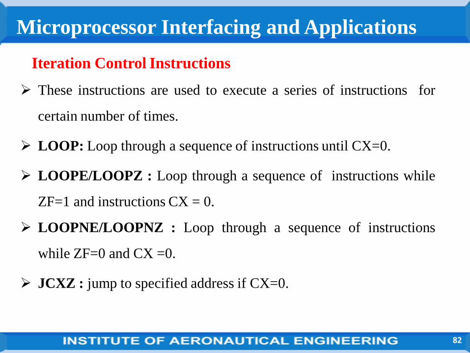
Iteration Control Instructions
These instructions are used to execute a series of instructions for
certain number of times.
LOOP: Loop through a sequence of instructions until CX=0.
LOOPE/LOOPZ : Loop through a sequence of instructions while
ZF=1 and instructions CX = 0.
LOOPNE/LOOPNZ : Loop through a sequence of instructions
while ZF=0 and CX =0.
JCXZ : jump to specified address if CX=0.
82
Microprocessor Interfacing and Applications

Interrupt Instructions
Two types of interrupt instructions:
Hardware Interrupts (External Interrupts)
Software Interrupts (Internal Interrupts and Instructions)
Hardware Interrupts:
• INTR is a maskable hardware interrupt.
• NMI is a non-maskable interrupt.
83
Microprocessor Interfacing and Applications

Software Interrupts
• INT : Interrupt program execution, call service procedure
• INTO : Interrupt program execution if OF=1
• IRET: Return from interrupt service procedure to main program.
84
Microprocessor Interfacing and Applications

High Level Language Interface Instructions
ENTER : enter procedure.
LEAVE: Leave procedure.
BOUND: Check if effective address within specified array
bounds.
85
Microprocessor Interfacing and Applications

Processor Control Instructions
I. Flag set/clear instructions
STC: Set carry flag CF to 1
CLC: Clear carry flag CF to 0
CMC: Complement the state of the carry flag CF
STD: Set direction flag DF to 1 (decrement string pointers)
CLD: Clear direction flag DF to 0
STI: Set interrupt enable flag to 1(enable INTR input)
CLI: Clear interrupt enable Flag to 0 (disable INTR input)
86
Microprocessor Interfacing and Applications

II. External Hardware synchronization instructions
HLT: Halt (do nothing) until interrupt or reset.
WAIT: Wait (Do nothing) until signal on the test pin is low.
ESC: Escape to external coprocessor such as 8087 or 8089.
LOCK: An instruction prefix. Prevents another processor from taking
the bus while the adjacent instruction executes.
NOP: No operation. This instruction simply takes up three clock
cycles and does no processing.
87
Microprocessor Interfacing and Applications

Assembler Directives
88
Microprocessor Interfacing and Applications

Assembler Directives
ASSUME
DB -
DD -
DQ -
DT -
DW -
Defined Byte.
Defined Double Word
Defined Quad Word
Define Ten Bytes
Define Word
89
Microprocessor Interfacing and Applications

ASSUME Directive- The ASSUME directive is used to tell the
assembler that the name of the logical segment should be used for a
specified segment. The 8086 works directly with only 4 physical
segments: a Code segment, a data segment, a stack segment, and an
extra segment.
Example:
ASUME CS:CODE ;This tells the assembler that the logical
segment named CODE contains the instruction statements for the
program and should be treated as a code segment.
ASSUME DS:DATA ;This tells the assembler that for any
instruction which refers to a data in the data segment, data will
found in the logical segment DATA.
90
Microprocessor Interfacing and Applications

DB - DB directive is used to declare a byte- type variable or to
store a byte in memory location.
Example:
1. PRICE DB 49h, 98h, 29h ;Declare an array of 3 bytes,
named as PRICE and initialize.
2. NAME DB ‘ABCDEF’ ;Declare an array of 6
bytes and initialize with ASCII code for letters
3. TEMP DB 100 DUP(?);Set 100 bytes of storage in
memory and give it the name as TEMP, but leave the 100 bytes
uninitialized. Program instructions will load values into these
locations.
91
Microprocessor Interfacing and Applications

DW-The DW directive is used to define a variable of type word or
to reserve storage location of type word in memory.
Example:
MULTIPLIER DW 437Ah ; this declares a variable of type word and named it as MULTIPLIER. This variable is initialized with the value 437Ah when it is loaded into memory to run.
EXP1 DW 1234h, 3456h, 5678h ; this declares an array of 3
words and initialized with specified values.
STOR1 DW 100 DUP(0); Reserve an array of 100 words of memory
and initialize all words with 0000.Array is named as STOR1.
92
Microprocessor Interfacing and Applications

END - END directive is placed after the last statement
of a program to tell the assembler that this is the end of the program
module. The assembler will ignore any statement after an END
directive.
ENDP - ENDP directive is used along with the name of
the procedure to indicate the end of a procedure to the assembler
Example:
• SQUARE_NUM PROCE ; It start the procedure
;Some steps to find the square root of a number
• SQUARE_NUM ENDP ;Hear it is the End for the procedure
93
Microprocessor Interfacing and Applications

END -
ENDP -
ENDS -
EQU -
EVEN -
EXTRN -
End Program
End Procedure
End Segment
Equate
Align on Even Memory Address
94
Microprocessor Interfacing and Applications

ENDS - This ENDS directive is used with name of the segment to
indicate the end of that logic segment.
Example: CODE SEGMENT ;Hear it Start the logic segment
containing code ;
CODE ENDS ;End of segment named as CODE
GLOBAL - Can be used in place of a PUBLIC directive or in place
of an EXTRN directive.
95
Microprocessor Interfacing and Applications

GROUP-Used to tell the assembler to group the logical statements
named after the directive into one logical group segment, allowing
the contents of all the segments to be accessed from the same group
segment base.
INCLUDE - Used to tell the assembler to insert a block of source
code from the named file into the current source module.
LABEL- Used to give a name to the current value in the location
counter.
NAME- Used to give a specific name to each assembly module
when programs consisting of several modules are written.
E.g.: NAME PC_BOARD
96
Microprocessor Interfacing and Applications

OFFSET- Used to determine the offset or displacement of a nameddata item or procedure from the start of the segment which containsit.
E.g.: MOV BX, OFFSET PRICES
ORG- The location counter is set to 0000 when the assemblerstarts reading a segment. The ORG directive allows setting adesired value at any point in the program.
E.g.: ORG 2000H
PROC- Used to identify the start of a procedure.
E.g.: SMART_DIVIDE PROC FAR
PTR- Used to assign a specific type to a variable or to a label.
E.g.: INC BYTE PTR[BX] tells the
97
Microprocessor Interfacing and Applications

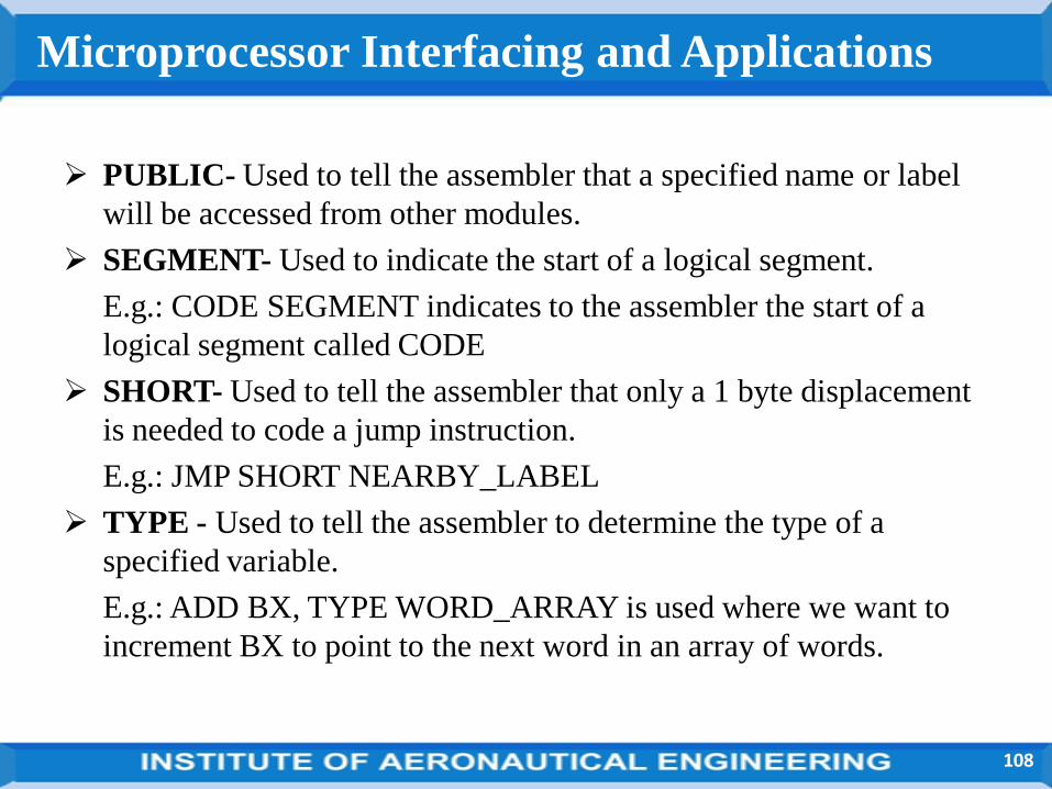
PUBLIC- Used to tell the assembler that a specified name or label
will be accessed from other modules.
SEGMENT- Used to indicate the start of a logical segment.
E.g.: CODE SEGMENT indicates to the assembler the start of a
logical segment called CODE
SHORT- Used to tell the assembler that only a 1 byte displacement
is needed to code a jump instruction.
E.g.: JMP SHORT NEARBY_LABEL
TYPE - Used to tell the assembler to determine the type of a
specified variable.
E.g.: ADD BX, TYPE WORD_ARRAY is used where we want to
increment BX to point to the next word in an array of words.
98
Microprocessor Interfacing and Applications

Assembler Directives:
ASSUME
DB -
DD -
DQ -
DT -
DW -
Defined Byte.
Defined Double Word
Defined Quad Word
Define Ten Bytes
Define Word
99
Microprocessor Interfacing and Applications

ASSUME Directive- The ASSUME directive is used to tellthe assembler that the name of the logical segment should beused for a specified segment. The 8086 works directly withonly 4 physical segments: a Code segment, a data segment, astack segment, and an extra segment.
Example:
ASUME CS:CODE ;This tells the assembler that thelogical segment named CODE contains the instructionstatements for the program and should be treated as a codesegment.
ASUME DS:DATA ;This tells the assembler that for any
instruction which refers to a data in the data segment, data will
found in the logical segment DATA.
100
Microprocessor Interfacing and Applications

DB - DB directive is used to declare a byte- type variable or to
store a byte in memory location.
Example:
1. PRICE DB 49h, 98h, 29h ;Declare an array of 3 bytes,
named as PRICE and initialize.
2. NAME DB ‘ABCDEF’ ;Declare an array of 6
bytes and initialize with ASCII code for letters
3. TEMP DB 100 DUP(?);Set 100 bytes of storage in
memory and give it the name as TEMP, but leave the 100 bytes
uninitialized. Program instructions will load values into these
locations.
101
Microprocessor Interfacing and Applications

DW - The DW directive is used to define a variable of type word or to reserve storage location of type word in memory.
Example:
• MULTIPLIER DW 437Ah ; this declares a variable of type word and named it as MULTIPLIER. This variable is initialized with the value 437Ah when it is loaded into memory to run.
• EXP1 DW 1234h, 3456h, 5678h ; this declares an array of 3 words and initialized with specified values.
• STOR1 DW 100 DUP(0); Reserve an array of 100 words of memory and initialize all words with 0000.Array is named as STOR1.
102
Microprocessor Interfacing and Applications

END - END directive is placed after the last statement
of a program to tell the assembler that this is the end of the program
module. The assembler will ignore any statement after an END
directive.
ENDP - ENDP directive is used along with the name of
the procedure to indicate the end of a procedure to the assembler
Example:
• SQUARE_NUM PROCE ; It start the procedure
;Some steps to find the square root of a number
• SQUARE_NUM ENDP ;Hear it is the End for the procedure
103
Microprocessor Interfacing and Applications

END -
ENDP -
ENDS -
EQU -
EVEN -
EXTRN
End Program
End Procedure
End Segment
Equate
Align on Even Memory Address
104
Microprocessor Interfacing and Applications

ENDS - This ENDS directive is used with name of the segment to
indicate the end of that logic segment.
Example: CODE SEGMENT ;Hear it Start the logic segment
containing code ;
Some instructions statements to perform the logical operation
CODE ENDS ;End of segment named as CODE
105
Microprocessor Interfacing and Applications

GROUP-Used to tell the assembler to group the logical statements
named after the directive into one logical group segment, allowing
the contents of all the segments to be accessed from the same group
segment base.
INCLUDE - Used to tell the assembler to insert a block of source
code from the named file into the current source module.
LABEL- Used to give a name to the current value in the location
counter.
NAME- Used to give a specific name to each assembly module
when programs consisting of several modules are written.
E.g.: NAME PC_BOARD
106
Microprocessor Interfacing and Applications

OFFSET- Used to determine the offset or displacement of a named
data item or procedure from the start of the segment which contains
it.
E.g.: MOV BX, OFFSET PRICES
ORG- The location counter is set to 0000 when the assembler
starts reading a segment. The ORG directive allows setting a
desired value at any point in the program.
E.g.: ORG 2000H
PROC- Used to identify the start of a procedure.
E.g.: SMART_DIVIDE PROC FAR
PTR- Used to assign a specific type to a variable or to a label.
E.g.: INC BYTE PTR[BX]
107
Microprocessor Interfacing and Applications
PUBLIC- Used to tell the assembler that a specified name or label
will be accessed from other modules.
SEGMENT- Used to indicate the start of a logical segment.
E.g.: CODE SEGMENT indicates to the assembler the start of a
logical segment called CODE
SHORT- Used to tell the assembler that only a 1 byte displacement
is needed to code a jump instruction.
E.g.: JMP SHORT NEARBY_LABEL
TYPE - Used to tell the assembler to determine the type of a
specified variable.
E.g.: ADD BX, TYPE WORD_ARRAY is used where we want to
increment BX to point to the next word in an array of words.
108
Microprocessor Interfacing and Applications

Simple Programs of 8086
109
Microprocessor Interfacing and Applications

Microprocessor Interfacing and Applications
DATA SEGMENT
A1 DB 50H
A2 DB 51H
RES DB ?
DATA ENDS
CODE SEGMENT
ASSUME CS: CODE, DS:DATA
START: MOV AX,DATA
MOV DS,AX
MOV AL,A1
MOV BL,A2
ADD AL,BL
MOV RES,AL
MOV AX,4C00H
INT 21H
CODE ENDS
END START
110

Microprocessor Interfacing and Applications
DATA SEGMENT
FIRST DW 03H
SEC DW 01H
DATA ENDS
CODE SEGMENT
ASSUME CS:CODE,DS:DATA
START: MOV AX,DATA
MOV DS,AX
MOV AX,SEC
MOV CX,FIRST
L1: MUL CX
DEC CX
JCXZ L2
JMP L1
L2: INT 3H
CODE ENDS
END START
111

Microprocessor Interfacing and Applications
DATA SEGMENT
NUM DW 5H
RES DW ?
DATA ENDS
CODE SEGMENT
ASSUME CS: CODE, DS: DATA
START: MOV AX,DATA
MOV DS,AX
MOV CX,NUM
MOV BX,00
L1: MOV AX,CX
MUL CX
ADD BX,AX
DEC CX
JNZ L1
MOV RES,BX
INT 3H
CODE ENDS
END START
112

Procedures:
• While writing programs, it may be the case that a particular
sequence of instructions is used several times. To avoid writing the
sequence of instructions again and again in the program, the same
sequence can be written as a separate subprogram called a
procedure.
Defining Procedures:
• Assembler provides PROC and ENDP directives in order to define
procedures. The directive PROC indicates beginning of a procedure.
Its general form is:
Procedure name PROC [NEAR|FAR]
113
Microprocessor Interfacing and Applications

Passing parameters to and from procedures:
The data values or addresses passed between procedures and main
program are called parameters. There are four ways of passing
parameters:
Passing parameters in registers
Passing parameters in dedicated memory locations
Passing parameters with pointers passed in registers
Passing parameters using the stack
114
Microprocessor Interfacing and Applications

MACROS:
When the repeated group of instruction is too short or not suitable to be
implemented as a procedure, we use a MACRO. A macro is a group of
instructions to which a name is given. Each time a macro is called in a
program, the assembler will replace the macro name with the group of
instructions.
Defining MACROS:
Before using macros, we have to define them. MACRO directive
informs the assembler the beginning of a macro. The general form is:
Macro_name MACRO argument1, argument2, …
Arguments are optional. ENDM informs the assembler the end of the
macro. Its general form is : ENDM
115
Microprocessor Interfacing and Applications

Procedures Macros
Accessed by CALL and RET
mechanism during program execution
Accessed by name given to macro
when
defined during assembly
Machine code for instructions only put
in memory once
Machine code generated for
instructions
each time called
Parameters are passed in registers,
memory locations or stack
Parameters passed as part of statement
which calls macro
Procedures uses stack Macro does not utilize stack
A procedure can be defined anywhere
in program using the directives PROC
and ENDP
A macro can be defined anywhere in
program using the directives MACRO
and ENDM
Procedures takes huge memory for
CALL(3 bytes each time CALL is
used) instruction
Length of code is very huge if macro’s
are called for more number of times
116
Microprocessor Interfacing and Applications

UNIT-II
PIN DIAGRAM OF 8086 AND AEESMBLY
LANGUAGE PROGRAMMING
117
Microprocessor Interfacing and Applications

Minimum mode operation in 8086
118
Microprocessor Interfacing and Applications

Minimum mode operation in 8086:
119
Microprocessor Interfacing and Applications

In a minimum mode 8086 system, the microprocessor 8086 is
operated in minimum mode by strapping its MN/MX pin to logic 1.
In this mode, all the control signals are given out by the
microprocessor chip itself. There is a single microprocessor in the
minimum mode system.
The remaining components in the system are latches, transceivers,
clock generator, memory and I/O devices. Some type of chip
selection logic may be required for selecting memory or I/O devices,
depending upon the address map of the system.
Latches are generally buffered output D-type flip-flops like
74LS373 or 8282. They are used for separating the valid address
from the multiplexed address/data signals and are controlled by the
ALE signal generated by 8086.
120
Microprocessor Interfacing and Applications

Transceivers are the bidirectional buffers and sometimes they are
called as data amplifiers. They are required to separate the valid data
from the time multiplexed address/data signals.
They are controlled by two signals namely, DEN and DT/R.
The DEN signal indicates the direction of data, i.e. from or to the
processor. The system contains memory for the monitor and users
program storage.
Usually, EPROM is used for monitor storage, while RAM for users
program storage. A system may contain I/O devices.
121
Microprocessor Interfacing and Applications

Maximum mode operation in 8086
122
Microprocessor Interfacing and Applications

• In the maximum mode, the 8086 is operated by strapping the MN/MX pin to ground.
• In this mode, the processor derives the status signal S2, S1, S0. Another chip called bus controller derives the control signal using this status information.
• In the maximum mode, there may be more than one microprocessor in the system configuration.
• The components in the system are same as in the minimum mode system.
• The basic function of the bus controller chip IC8288 is to derive control signals like RD and WR (for memory and I/O devices), DEN, DT/R, ALE etc. using the information by the processor on the status lines.
• The bus controller chip has input lines S2, S1, S0 and CLK. These inputs to 8288 are driven by CPU.
123
Microprocessor Interfacing and Applications

Maximum mode
124
Microprocessor Interfacing and Applications

• It derives the outputs ALE, DEN, DT/R, MRDC, MWTC, AMWC, IORC, IOWC and AIOWC. The AEN, IOB and CEN pins are especially useful for multiprocessor systems.
• AEN and IOB are generally grounded. CEN pin is usually tied to +5V. The significance of the MCE/PDEN output depends upon the status of the IOB pin.
• If IOB is grounded, it acts as master cascade enable to control cascade 8259A, else it acts as peripheral data enable used in the multiple bus configurations.
• INTA pin used to issue two interrupt acknowledge pulses to the interrupt controller or to an interrupting device.
• IORC, IOWC are I/O read command and I/O write command signals respectively.
• These signals enable an IO interface to read or write the data from or to the address port.
• The MRDC, MWTC are memory read command and memory write command signals respectively and may be used as memory read or write signals.
125
Microprocessor Interfacing and Applications

• The MRDC, MWTC are memory read command and memory write command signals respectively and may be used as memory read or write signals.
• All these command signals instructs the memory to accept or send data from or to the bus.
• For both of these write command signals, the advanced signals namely AIOWC and AMWTC are available.
• Here the only difference between in timing diagram between minimum mode and maximum mode is the status signals used and the available control and advanced command signals.
• R0, S1, S2 are set at the beginning of bus cycle.8288 bus controller will output a pulse as on the ALE and apply a required signal to its DT / R pin during T1.
• In T2, 8288 will set DEN=1 thus enabling transceivers, and for an input it will activate MRDC or IORC. These signals are activated until T4. For an output, the AMWC or AIOWC is activated from T2 to T4 and MWTC or IOWC is activated from T3 to T4.
126
Microprocessor Interfacing and Applications

Timing diagram for minimum
mode
127
Microprocessor Interfacing and Applications

Write Cycle Timing Diagram for Minimum Mode
128
Microprocessor Interfacing and Applications

• The working of the minimum mode configuration system can be
better described in terms of the timing diagrams rather than
qualitatively describing the operations.
• The opcode fetch and read cycles are similar. Hence the timing
diagram can be categorized in two parts, the first is the timing
diagram for read cycle and the second is the timing diagram for
write cycle.
129
Microprocessor Interfacing and Applications

Bus Request and Bus Grant Timings in Minimum Mode System of 8086
130
Microprocessor Interfacing and Applications

Timing diagram for maximum
mode
131
Microprocessor Interfacing and Applications

Memory Read Timing Diagram in Maximum Mode of 8086
132
Microprocessor Interfacing and Applications

Memory Write Timing in Maximum mode of 8086
133
Microprocessor Interfacing and Applications

Memory interfacing to 8086 (Static
RAM and EPROM)
134
Microprocessor Interfacing and Applications

• Interface two 4Kx8 EPROMS and two 4Kx8 RAM chips with 8086. select suitable maps.
135
Microprocessor Interfacing and Applications

136
Microprocessor Interfacing and Applications

137
Microprocessor Interfacing and Applications

Memory interfacing to 8086
(Static RAM and EPROM)
138
Microprocessor Interfacing and Applications

• Interface two 4Kx8 EPROMS and two 4Kx8 RAM chips with 8086. select suitable maps.
139
MICROPROCESSORS AND
INTERFACING
Microprocessor Interfacing and Applications

140
Microprocessor Interfacing and Applications

141
Microprocessor Interfacing and Applications

Need for DMA,DMA Data
transfer Method
142
Microprocessor Interfacing and Applications

Need For DMA
• Direct memory access (DMA) is a feature of modern computer
systems that allows certain hardware subsystems to read/write data
to/from memory without microprocessor intervention, allowing the
processor to do other work.
• Used in disk controllers, video/sound cards etc, or between memory
locations.
• Typically, the CPU initiates DMA transfer, does other operations
while the transfer is in progress, and receives an interrupt from the
DMA controller once the operation is complete.
• Can create cache coherency problems (the data in the cache may be
different from the data in the external memory after DMA)
143
Microprocessor Interfacing and Applications

• DMA Data Transfer Method
144
Microprocessor Interfacing and Applications

• The I/O device asserts the appropriate DRQ signal for the channel.
• The DMA controller will enable appropriate channel, and ask the
CPU to release the bus so that the DMA may use the bus. The DMA
requests the bus by asserting the HOLD signal which goes to the
CPU.
• The CPU detects the HOLD signal, and will complete executing the
current instruction. Now all of the signals normally generated by the
CPU are placed in a tri-stated condition (neither high or low) and
then the CPU asserts the HLDA signal which tells the DMA
controller that it is now in charge of the bus.
• The CPU may have to wait (hold cycles).
145
Microprocessor Interfacing and Applications

• DMA activates its -MEMR, -MEMW, -IOR, -IOW output signals,
and the address outputs from the DMA are set to the target address,
which will be used to direct the byte that is about to transferred to a
specific memory location.
• The DMA will then let the device that requested the DMA transfer
know that the transfer is commencing by asserting the -DACK
signal.
• The peripheral places the byte to be transferred on the bus Data
lines.
• Once the data has been transferred, The DMA will de-assert the -
DACK2 signal, so that the FDC knows it must stop placing data on
the bus.
146
Microprocessor Interfacing and Applications

• The DMA will now check to see if any of the other DMA channels
have any work to do. If none of the channels have their DRQ lines
asserted, the DMA controller has completed its work and will now
tri-state the -MEMR, -MEMW, -IOR, -IOW and address signals.
• Finally, the DMA will de-assert the HOLD signal. The CPU sees
this, and de-asserts the HOLDA signal. Now the CPU resumes
control of the buses and address lines, and it resumes executing
instructions and accessing main memory and the peripherals.
147
Microprocessor Interfacing and Applications

8237-DMA Controller
148
Microprocessor Interfacing and Applications

• Pin diagram
149
Microprocessor Interfacing and Applications

• Block Diagram
150
Microprocessor Interfacing and Applications

8237 Internal Registers
• CAR
• The current address register holds a 16-bit memory address used for
the DMA transfer.
• each channel has its own current address
register for this purpose.
• When a byte of data is transferred during a DMA operation, CAR is
either incremented
or decremented. depending on how it is programmed
• CWCR
• The current word count register programs a channel for the number
of bytes to transferred during a DMA action.
151
Microprocessor Interfacing and Applications

CR(Command Register)
• The command register programs the operation of the 8237 DMA
controller.
• The register uses bit position 0 to select the memory-to-memory
DMA transfer mode.
– Memory-to-memory DMA transfers use DMA channel
– DMA channel 0 to hold the source address
– DMA channel 1 holds the destination address
152
Microprocessor Interfacing and Applications

153
Microprocessor Interfacing and Applications

BA and BWC
• The base address (BA) and base word count (BWC) registers are
used when auto-initialization is selected for a channel.
• In auto-initialization mode, these registers are used to reload the
CAR and CWCR after the DMA action is completed.
MR (Mode Register)
• The mode register programs the mode of operation for a channel.
• Each channel has its own mode register as selected by bit positions 1
and 0.
– Remaining bits of the mode register select operation, auto-
initialization, increment/decrement, and mode for the channel
154
Microprocessor Interfacing and Applications

155
Microprocessor Interfacing and Applications

RR(Request Register)
• The request register is used to request
a DMA transfer via software.
• very useful in memory-to-memory transfers, where an external
signal is not available to begin the DMA transfer
156
Microprocessor Interfacing and Applications

157
Microprocessor Interfacing and Applications

MR(Mask Register)
• The mask register set/reset sets or clears the channel mask.
• if the mask is set, the channel is disabled.
• The RESET signal sets all channel masks
to disable them
158
Microprocessor Interfacing and Applications

MSR
The mask register clears or sets all of
the masks with one command instead of individual channels, as with
the MRSR.
159
Microprocessor Interfacing and Applications

SR(Status Register)
• The status register shows status of each DMA channel. The TC bits
indicate if the channel has reached its terminal count (transferred all
its bytes).
• When the terminal count is reached, the DMA transfer is terminated
for most modes
of operation.
• The request bits indicate whether the DREQ input for a given
channel is active.
160
Microprocessor Interfacing and Applications

161
Microprocessor Interfacing and Applications

DMA Controller-8257
162
Microprocessor Interfacing and Applications

Features of 8257
• Here is a list of some of the prominent features of 8257 −
• It has four channels which can be used over four I/O devices.
• Each channel has 16-bit address and 14-bit counter.
• Each channel can transfer data up to 64kb.
• Each channel can be programmed independently.
• Each channel can perform read transfer, write transfer and verify
transfer operations.
• It generates MARK signal to the peripheral device that 128 bytes
have
• been transferred.
• It requires a single phase clock.
• Its frequency ranges from 250Hz to 3MHz.
163
Microprocessor Interfacing and Applications

8257 Pin Description
• The following image shows the pin diagram of a 8257 DMA controller
164
Microprocessor Interfacing and Applications

165
Microprocessor Interfacing and Applications

• Block Diagram of 8257
166
Microprocessor Interfacing and Applications

• Terminal Count Register:
167
Microprocessor Interfacing and Applications

• Mode Set Register:
168
Microprocessor Interfacing and Applications

• Status Register:
169
Microprocessor Interfacing and Applications

170
Microprocessor Interfacing and Applications

Assembly language programs
using logical, branch& call
instructions
171
Microprocessor Interfacing and Applications

Programs using logical ,Branch and call instructions.Data segment
Org 2000h Mov [di],ax
N1 dw 5678h Int 03h
N2 dw 2345h Code ends
Data ends End
Code segment
Assume cs:code,ds:dats
Mov ax,data
Mov ds,ax
Mov DI,2040h
Mov ax,N1
AND ax,bx
Microprocessor Interfacing and Applications
172

2)Data segment• Org 2000h• N1 dw 5678h• N2 dw 2345h• Data ends• Code segment• Assume cs:code,ds:dats• Mov ax,data• Mov ds,ax• Mov DI,2040h• Mov ax,N1• MOV bx,N2• OR ax,bx• Mov [di],ax• Int 03h• Code ends• End
Microprocessor Interfacing and Applications
173

3)Data segment• Org 2000h• N1 dw 5678h• N2 dw 2345h• Data ends• Code segment• Assume cs:code,ds:dats• Mov ax,data• Mov ds,ax• Mov DI,2040h• Mov ax,N1• MOV bx,N2• xor ax,bx• Mov [di],ax• Int 03h• Code ends• End
Microprocessor Interfacing and Applications
174

4)Data segment
• Org 2000h
• N1 dw 5678h
• Data ends
• Code segment
• Assume cs:code,ds:dats
• Mov ax,data
• Mov ds,ax
• Mov DI,2040h
• Mov ax,N1
• SHL ax,04
• Mov [di],ax
• Int 03h
• Code ends
• End
Microprocessor Interfacing and Applications
175

Assembly language programs using logical, branch& call
instructions
Microprocessor Interfacing and Applications
176

Programs using logical ,Branch and call instructions.1)Data segment
• Org 2000h . Mov [di],ax
• N1 dw 5678h . Int 03h
• Data ends . Code ends
• Code segment . End
• Assume cs:code,ds:dats
• Mov ax,data
• Mov ds,ax
• Mov DI,2040h
• Mov ax,N1
• SHR ax,04
Microprocessor Interfacing and Applications
177

2)Data segment• Org 2000h• N1 dw 5678h• Data ends• Code segment• Assume cs:code,ds:dats• Mov ax,data• Mov ds,ax• Mov DI,2040h• Mov ax,N1• ROR ax,02• Mov [di],ax• Int 03h• Code ends• End
Microprocessor Interfacing and Applications
178

3)Data segment• Org 2000h• N1 dw 5678h• Data ends• Code segment• Assume cs:code,ds:dats• Mov ax,data• Mov ds,ax• Mov DI,2040h• Mov ax,N1• RCR ax,03• Mov [di],ax• Int 03h• Code ends• End
Microprocessor Interfacing and Applications
179

4)Data segment
• Org 2000h
• N1 dw 5678h
• Data ends
• Code segment
• Assume cs:code,ds:dats
• Mov ax,data
• Mov ds,ax
• Mov DI,2040h
• Mov ax,N1
• RCL ax,04
• Mov [di],ax
• Int 03h
• Code ends
• End
Microprocessor Interfacing and Applications
180

Sorting
181
Microprocessor Interfacing and Applications

Assembly language program to sort the given numbers in Ascending order
ASSUME CS: CODE
CODE SEGMENT
START: MOV AX,0000H
MOV CH, 0004H
DEC CH
UP1: MOV CL, CH
MOV SI, 2000H
UP: MOV AL, [SI]
INC SI
CMP AL, [SI]
182
Microprocessor Interfacing and Applications

JC DOWN
XCHG AL, [SI]
DEC SI
MOV [SI], AL
INC SI
DOWN: DEC CL
JNZ UP
DEC CH
JNZ UP1
INT 3
CODE ENDS
END START183
Microprocessor Interfacing and Applications

Assembly language program to sort the given numbers in Descending order
ASSUME CS: CODE
CODE SEGMENT
START: MOV AX, 0000H
MOV CH, 0004H
DEC CH
UP1: MOV CL, CH
MOV SI, 2000H
UP: MOV AL, [SI]
INC SI
CMP AL, [SI] 184
Microprocessor Interfacing and Applications

JNC DOWN
XCHG AL, [SI]
DEC SI
MOV [SI], AL
INC SI
DOWN: DEC CL
JNZ UP
DEC CH
JNZ UP1
I NT 3
CODE ENDSEND START
185
Microprocessor Interfacing and Applications

Evaluation of arithmetic expressions
186
Microprocessor Interfacing and Applications

An Assembly program for performing the following operation Z= ((A-B)/10*C)
DATA SEGMENTA DB 60B DB 20C DB 5Z DW?ENDSCODE SEGMENTASSUME DS: DATA CS: CODE
START: MOV AX, DATAMOV DS, AXMOV AH, 0 ; Clear content of AXMOV AL, A ; Move A to register AL
187
Microprocessor Interfacing and Applications

SUB AL, B ; Subtract AL and B
MUL C ; Multiply C to AL
MOV BL, 10 ; Move 10 to register BL
DIV BL ; Divide AL content by BL
MOV Z, AX ; Move content of AX to Z
MOV AH, 4CH
INT 21H
ENDS
END START
188
Microprocessor Interfacing and Applications

An Assembly program for performing the following operation C = (A + B)^2DATA SEGMENTA DB 60B DB 20C EQU 2000H ENDSCODE SEGMENTASSUME DS: DATA CS: CODE
START: MOV AX, DATAMOV DS, AXMOV AX, A ; Move A to Register Ax ADD AX, B ; Add B to A IMUL AX ; Square (A+B) MOV [C], AX ; Move (A+B) ^2 to C in BX.INT 21H
ENDSEND START
189
Microprocessor Interfacing and Applications
Evaluation of string manipulation
190
Microprocessor Interfacing and Applications

Program For String Transfer
DATA SEGMENT ; start of data segment
STR1 DB 'HOW ARE YOU'
LEN EQU $-STR1
STR2 DB 20 DUP (0)
DATA ENDS ; end of data segment
CODE SEGMENT ; start of code segment
ASSUME CS: CODE, DS: DATA, ES: DATA
START: MOV AX, DATA ; initialize data segment
MOV DS, AX
191
Microprocessor Interfacing and Applications

MOV ES, AX ; initialize extra segment for string operations
LEA SI, STR1 ; SI points to starting address of string at ; STR1
LEA DI, STR2 ; DI points to starting address of where the string has to be transferred
MOV CX, LEN ; load CX with length of the string
CLD ; clear the direction flag for auto increment SI; and DI
REP MOVSB ; the source string is moved to destination address till CX=0(after every move CX is; decremented)
MOV AH, 4CH ; terminate the process
INT 21H
CODE ENDS ; end of code segment
END START
192
Microprocessor Interfacing and Applications

Program To Reverse A String
DATA SEGMENT ; start of data segment
STR1 DB 'HELLO'
LEN EQU $-STR1
STR2 DB 20 DUP (0)
DATA ENDS ; end of data segment
CODE SEGMENT ; start of code segment
ASSUME CS: CODE, DS: DATA, ES: DATA
START: MOV AX, DATA ; initialize data segment
MOV DS, AX
MOV ES, AX
193
Microprocessor Interfacing and Applications

LEA SI, STR1
LEA DI, STR2+LEN-1
MOV CX, LEN
UP: CLD
LODSB
STD
STOSB
LOOP UP
MOV AH, 4CH
INT 21H
CODE ENDS
END START
194
Microprocessor Interfacing and Applications

UNIT-III
8255 PROGRAMMABLE
PERIPHERAL INTERFACE (PPI)
195
Microprocessor Interfacing and Applications

Introduction to 8255 (PIO)
196
Microprocessor Interfacing and Applications

84
8255-PROGRAMMABLE PERIPHERALINTERFACE
It has 24 input/output lines
24 lines divided into 3 ports
• Port A(8 bit)
• Port B(8 bit)
• Port C upper(4 bit), Port C Lower (4 bit)
All the above 3 ports can act as input or output ports
197
Microprocessor Interfacing and Applications

85
Block Diagram
Figure: Block Diagram of 8255(PIC)
198
Microprocessor Interfacing and Applications

Data Bus buffer
It is a 8-bit bidirectional Data bus.
Used to interface between 8255 data bus with system bus.
The internal data bus and Outer pins D0-D7 pins are connected in
internally.
The direction of data buffer is decided by Read/Control Logic.
86 199
Microprocessor Interfacing and Applications

Read/Write Control Logic
This is getting the input signals from control bus and Address Bus.
Control signal are RD and WR.
Address signals are A0, A1, and CS
8255 operation is enabled or disabled by CS.
Group A and B get the Control Signal from CPU and send the command to
the individual control blocks.
Group A send the control signal to port A and Port C (Upper) PC7-PC4.
Group B send the control signal to port B and Port C (Lower) PC3-PC0.
87 200
Microprocessor Interfacing and Applications

PORT A:
This is a 8-bit buffered I/O latch.
It can be programmed by mode 0 , mode 1, mode 2 .
PORT B:
This is a 8-bit buffer I/O latch.
It can be programmed by mode 0 and mode 1.
PORT C:
This is a 8-bit Unlatched buffer Input and an Output latch.
It is spitted into two parts.
It can be programmed by bit set/reset operation.88 201
Microprocessor Interfacing and Applications

Introduction to 8255 (PIO)
202
Microprocessor Interfacing and Applications

90
8255-PROGRAMMABLE PERIPHERAL INTERFACE
8255 Pin Diagram
203
Microprocessor Interfacing and Applications

Pin Description of 8255
PA7-PA0: These are eight port A lines that acts as either latched
output or buffered input lines depending upon the control
word loaded into the control word register.
PC7-PC4: Upper nibble of port C lines. They may act as either output
latches or input buffers lines. This port also can be used for
generation of handshake lines in mode 1 or mode 2.
PC3-PC0: These are the lower port C lines, other details are the
same as PC7-PC4 lines.
PB0-PB7: These are the eight port B lines which are used as
latched output lines or buffered input lines in the same way
as port A.
91 204
Microprocessor Interfacing and Applications

Pin Description of 8255
RD: This is the input line driven by the microprocessor and should
be low to indicate read operation to8255.
WR: This is an input line driven by the microprocessor. A low on
this line indicates write operation.
CS : This is a chip select line. If this line goes low, it enables the
8255 to respond to RD and WR signals, otherwise RD and WR signal
are neglected.
A1-A0: These are the address input lines and are driven by the
microprocessor.
RESET: The 8255 is placed into its reset state if this input line is a
logical 1. All peripheral ports are set to the input mode.
205
Microprocessor Interfacing and Applications

Various modes of 8255 operation and interfacing to 8086
206
Microprocessor Interfacing and Applications

Various modes of 8255:These are two basic modes of operation of 8255. I/O mode and Bit Set-
Reset mode (BSR).
In I/O Mode, the 8255 ports work as programmable I/O ports, while
in BSR mode only port C (PC0-PC7) can be used to set or reset its
individual port bits.
Under the I/O mode of operation, further there are three modes of
operation of 8255, so as to support different types of applications, mode
0, mode 1 and mode 2.
Mode 0 (Basic I/O mode): This mode is also called as basic
input/output Mode. This mode provides simple input and output
capabilities using each of the three ports. Data can be simply read from
and written to the input and output ports respectively, after appropriate
initialization.
207
Microprocessor Interfacing and Applications

Mode 1: (Strobed input/output mode) in this mode the
handshaking control the input and output action of the specified port.
Port C lines PC0-PC2, provide strobe or handshake lines for port B.
This group which includes port B and PC0-PC2 is called as group B
for Strobed data input/output. Port C lines PC3-PC5 provides strobe
lines for port A.
This group including port A and PC3-PC5 from group A. Thus port C
is utilized for generating handshake signals.
208
Microprocessor Interfacing and Applications

Mode 2 (Strobed bidirectional I/O): This mode of operation of 8255 is alsocalled as strobed bidirectional I/O. This mode of operation provides 8255with additional features for communicating with a peripheral device on an 8-bit data bus.
Handshaking signals are provided to maintain proper data flow andsynchronization between the data transmitter and receiver.
The interrupt generation and other functions are similar to mode 1.
BSR Mode:
In this mode any of the 8-bits of port C can be set or reset depending on D0of the control word. The bit to be set or reset is selected by bit select flagsD3, D2 and D1 of the CWR as given in table.
209
Microprocessor Interfacing and Applications

8255 interfacing with 8086:
210
MICROPROCESSORS AND INTERFACING

Interfacing Keyboard
211
Microprocessor Interfacing and Applications

Keyboard Interfacing:
In most keyboards, the key switches are connected in a
matrix of Rows and Columns.
Getting meaningful data from a keyboard requires three
major
tasks:
• Detect a key press
• Debounce the key press.
• Encode the key press (produce a standard code for the
pressed
key).
Logic ‘0’ is read by the microprocessor when the key is pressed.
212
Microprocessor Interfacing and Applications

Key Debounce:
Whenever a mechanical push-bottom is pressed or released once, the
mechanical components of the key do not change the position
smoothly; rather it generates a transient response. These may be
interpreted as the multiple pressures and responded accordingly.
213
Microprocessor Interfacing and Applications

214
Microprocessor Interfacing and Applications

215
Microprocessor Interfacing and Applications

216
Microprocessor Interfacing and Applications

Keyboard Interfacing Program:Assume that base address of 8255 is 8000H. So, addresses of ports will be as follows.
PORT A = 8000H (ROWS)
PORT B = 8002H (COLUMNS)
CONTROL PORT = 8006H
DATA SEGMENT
CNTLPRT EQU 8006H
PORTA EQU 8000H
PORT B EQU 8002H
DELAY EQU 6666 ; Delay constant for 20ms.
TABLE DB 30H, 31H, 32H, 33H, 34H, 35H, 36H, 37H, 38H, 39H, 41H, 42H, 43H, 44H, 45H, 46H
DATA ENDS
CODE SEGMENT
ASSUME CS: CODE, DS: DATA
START: MOV AX, DATA
MOV DS, AX.
MOV AL, 82H
MOV DX, CNTLPRT
OUT OX, AL
217
Microprocessor Interfacing and Applications

XOR AL, AL
MOV DX, PORTA
OUT DX, AL
MOV DX, PORTB
RDCOL: IN AL, DX
AND AL, 0FH
CMP AL, 0FH
JNE RDCOL
MOV CX, DELAY
SELF: LOOP SELF
IN AL,DX
AND AL, 0FH
CMP AL, 0FH
JNE RDCOL
RDAGN: IN AL,DX
AND AL, 0FH
JE RDAGN
MOV DX, DELAY
SELF1: LOOP SELF1
IN AL, DX
218
Microprocessor Interfacing and Applications

AND AL, 0FH
JE RDAGN
MOV AL, 0FEH
MOV BL, AL
ENROW: MOV DX, PORTA
OUT DX, AL
MOV DX, PORTB
IN AL, DX
AND AL, 0FH
CMP AL, 0FH
JNE CCODE
ROL BL, 1
MOV AL, BL
JMP ENROW
CCODE: MOV CL, 0
NXTCOL: ROR AL, 1
JNC CHKROW
INC CL
219
Microprocessor Interfacing and Applications

JMP NXTCOL
CHKROW: MOV DL, 0
NXTROW: ROR BL, 1
JNC CALADR
ADD DL, 4
JMP NXTROW
CALADR: ADD DL, CL
MOV AL, DL
LEA BX, TABLE
XLAT
INT 3
CODE ENDS
END START
220
Microprocessor Interfacing and Applications

Displays
221
Microprocessor Interfacing and Applications

Multiplexed Display:
222
Microprocessor Interfacing and Applications

Program for Multiplexed Display:
Assume base address of 8255 to be FFF8H
Address of port A = FFF8H
Address of port B = FFFAH
Address of control port = FFFEH
Algorithm:
1. Turn ON Q0 (Q1 to Q7 OFF) by applying a logical low to base of Q0 as transistor.
2. Send seven segment code for D0 (LSD) i.e., digit 0'
3. After 1ms turn OFF Q0 turn on Q1, so Q] will be ON and Q0 and Q2 ~ Q7 Will be OFF.
4. Send seven segment code for D1 i.e., digit 1.
5. After 1ms turn off Q1 and turn on Q2. So Q2 will be ON and Q0 Q1 and Q3-Q7 will be OFF.
6. Repeat the process for all 8 digits. It completes one cycle.
7. Start the cycle again.
223
Microprocessor Interfacing and Applications

Program for multiplexed Display:DATA SEGMENT
PORT A EQU OFFF8H
PORT B EQU OFFFAH
CNTLPRT EQU OFFFEH
DELAY EQU 012CH
DIGITS DB 1, 2,3,4,6,7,8,9
DATA ENDS
CODE SEGMENT
ASSUME CS: CODE, DS: DATA
START: MOV AX, DATA
MOV DS, AX
MOV DX, CNTL PRT
MOV AL, 80H
OUT DX, AL
REPEAT: MOV BH, 8
LEA SI, DIGITS
MOV BL, 0FEH
MOV AL, BL
MOV DX, PORT A
OUT DX, AL
MOV AL, [SI]
MOV DX, PORTB
OUT DX, AL
MOV CX, DELAY
SELF: LOOP SELF
INC SI
ROL BL, 1
DEC BH
JNZ BACK
JMP REPEAT
CODE ENDS
END START
224
Microprocessor Interfacing and Applications

8279 Stepper motor and actuators
225
Microprocessor Interfacing and Applications

Stepper motor is often used in computer systems. Normally DC and
AC motors move smoothly in a circular fashion.
Stepper motor is a DC motor, specially designed, which moves in
discrete or fixed step and thus complete one rotation of 360 degrees.
To rotate the shaft of the motor a sequence of pulses are applied to the
windings in a predefined sequence.
The number of pulses required to complete one rotation depends on
the number of teeth on the rotor. Hence rotation Per pulse sequence is
3600/NT where NT is the number of teeth on rotor.
If NT is equal to 200 then one step rotation will be of 1.80. The motors
are generally available to move in steps of 0.90 to 30° i.e. The step size
range is 0.90 -36°.
226
Microprocessor Interfacing and Applications

Programs for Stepper Motor Rotation:
1. Program to rotate the stepper motor continuously in clockwise
direction for following specification
NT = Number of teeth on rotor = 200
Speed of motor = 12 rotations/minute.
CPU frequency = 10MHz
227
Microprocessor Interfacing and Applications

DATA SEGMENT
PORTC EQU 8004H
CNTLPRT EQU 8006H
DELAY EQU 14705
DATA ENDS
CODE SEGMENT
ASSUME CS: CODE, DS: DATA
START: MOV AX, DATA
MOV DS, AX
MOV AL, 80H
MOV DX, CNTLPORT
OUT DX, AL
MOV AL, 33H
MOV DX, PORTC
BACK: OUT DX, AL
ROR AL, 1
MOV CX, DELAY
SELF: LOOP SELF
DELAY LOOP FOR 25Ms
JMP BACK
CODE ENDS
END START
228
Microprocessor Interfacing and Applications

Digital to analog converter
interfacing
229
Microprocessor Interfacing and Applications

DAC0800 8-bit Digital to Analog Converter
• The DAC 0800 is a monolithic 8-bit DAC manufactured by National
Semiconductor.
• It has settling time around 100ms and can operate on a range of
power supply voltages i.e. from 4.5V to +18V.
• Usually the supply V+ is 5V or +12V.
• The V-pin can be kept at a minimum of -12V.
230
Microprocessor Interfacing and Applications

231
Microprocessor Interfacing and Applications

Intersil‟s AD 7523 is a 16 pin DIP, multiplying digital to analo
converter, containing R-2R ladder(R=10KΩ) for digital to
analog conversion along with single pole double through NMOS
switches to connect the digital inputs to the ladder.
232
Microprocessor Interfacing and Applications

Pin Diagram of AD7523
• The supply range extends from +5V to +15V , while Vref
may be anywhere between -10V to +10V. The maximum
analog output voltage will be +10V, when all the digital
inputs are at logic high state. Usually a Zener is connected
between OUT1 and OUT2 to save the DAC from negative
transients.
• An operational amplifier is used as a current to voltage
converter at the output of AD 7523 to convert the current
output of AD7523 to a proportional output voltage.
• It also offers additional drive capability to the DAC output.
An external feedback resistor acts to control the gain. One
may not connect any external feedback resistor, if no gain
control is required.
233
Microprocessor Interfacing and Applications

Pin Diagram of AD7523
234
Microprocessor Interfacing and Applications

Analog to digital converter
interfacing
235
Microprocessor Interfacing and Applications

Block Diagram of ADC 0808/0809
236
Microprocessor Interfacing and Applications

Pin Diagram of ADC 0808/0809
237
Microprocessor Interfacing and Applications

Timing Diagram Of ADC 0808.
238
Microprocessor Interfacing and Applications

Interfacing ADC0808 with 8086
239
Microprocessor Interfacing and Applications

Interrupt structure of 8086
240
Microprocessor Interfacing and Applications

Interrupt structure of 8086
241
Microprocessor Interfacing and Applications

Vector interrupt table, interrupt service routines
242
Microprocessor Interfacing and Applications

Vector interrupt table
243
Microprocessor Interfacing and Applications

Introduction to DOS and BIOS
interrupts
Microprocessor Interfacing and Applications
244

BIOS INTERRUPT
• INT 10H – Video Screen
– The option is chosen by putting a specific value in register AH
– The video screen is text mode is divided into 80 columns and 25
rows
– A row and column number are associated with each location on
the screen with the top left corner as 00,00 and the bottom right
corner as 24,79. The center of the screen is at 12,39 or (0C,27 in
hex)
– Specific registers has to be set to specific values before invoking
INT 10H
Microprocessor Interfacing and Applications
245

• Function 06 – clear the screen
• AH = 06 ; function number
• AL = 00 ; page number
• BH = 07 ; normal attribute
• CH = 00 ; row value of start point
• CL = 00 ; column value of start point
• DH = 24 ; row value of ending point
• DL = 79 ; column value of ending point
• Function 02 – setting the cursor to a specific location
• AH = 06 ; function number
• DH = row ; cursor
• DL = column ; position
Microprocessor Interfacing and Applications
246

• Function 03 – get the current cursor position
• AH = 03 ; function number
• BH= 00 ; currently viewed page
• The position is returned in DH = row and DL = column
•
• Function 0E – output a character to the screen
• AH = 0E ; function number
• AL = Character to be displayed
• BH = 00 ; currently viewed page
• BL = 00 ; default foreground color
Microprocessor Interfacing and Applications
247

• Function 09 – outputting a string of data to the monitor
• AH = 09 ; function number
• DX = offset address of the ASCII data to be displayed, data segment
is assumed
• The ASCII string must end with the dollar sign $
• Function 02 – outputting a single character to the monitor
• AH = 02 ; function number
• DL = ASCII code of the character to be displayed
• Function 01 – inputting a single character, with an echo
• AH = 01 ; function number.After the interrupt AL = ASCII code of
the input and is echoed to the monitor
Microprocessor Interfacing and Applications
248

• Function 0A – inputting a string of data from the keyboard
• AH = 0A ; function number
• DX = offset address at which the string of data is stored (buffer area), data
• segment is assumed and the string must end with <RETURN>
• After execution:
• DS:DX = buffer in bytes (n characters + 2)
• DS:DX+1 = number of entered characters excluding the return key
• DS:DX+2 = first character input
• · · ·
• DS:DX+n = last character input
• To set a buffer, use the following in the data segment:
• Buffer DB 10, ? , 10 DUP(FF)
Microprocessor Interfacing and Applications
249

• Function 07 – inputting a single character from the keyboard
without an echo
• AH = 07 ; function number
• Waits for a single character to be entered and provides it in AL
• INT16 – Keyboard Programming
• Function 01 – check for a key press without waiting for the user
• AH = 01
• Upon execution ZF = 0 if there is a key pressed
• Function 00 – keyboard read
• AH = 00
• Upon execution AL = ASCII character of the pressed key
• Note this function must follow function 01
Microprocessor Interfacing and Applications
250

8259 PIC architecture and
interfacing
Microprocessor Interfacing and Applications
251

Internal Structure of 8259A
INTEL 8259A Programmable Interrupt Controller
Microprocessor Interfacing and Applications
252

Data bus buffer:
• This 3- state, bidirectional 8-bit buffer is used to interface the 8259A to the
system data bus. Control words and status information from the
microprocessor to PIC and from PIC to microprocessor respectively, are
transferred through the data bus buffer.
Read/Write & Control Logic: The function of this block is to
accept output commands sent from the CPU. It contains the
initialization command word (ICW) registers and operation
command word (OCW) registers which store the various control
formats for device operation. This function block also allows the
status of 8259A to be transferred to the data bus.
Microprocessor Interfacing and Applications
253

• Interrupt Request Register (IRR): Interrupt request register (IRR)
stores all the interrupt inputs that are requesting service. It is an 8-bit
register – one bit for each interrupt request. Basically, it keeps track
of which interrupt inputs are asking for service. If an interrupt input
is unmasked, and has an interrupt signal on it, then the
corresponding bit in the IRR will be set. The content of this register
can be read to know the status of pending interrupts.
Microprocessor Interfacing and Applications
254

• Interrupt Mask Register (IMR): The IMR is used to disable
(Mask) or enable (Unmask) individual interrupt request inputs. This
is also an 8-bit register. Each bit in this register corresponds to the
interrupt input with the same number. The IMR operates on the IRR.
Masking of higher priority input will not affect the interrupt request
lines of lower priority. To unmask any interrupt the corresponding
bit is set ‘0’.
Microprocessor Interfacing and Applications
255

• In-service Register (ISR): The in-service register keeps track of
which interrupt inputs are currently being serviced. For each input
that is currently being serviced the corresponding bit of in-service
register (ISR) will be set. In 8259A, during the service of an
interrupt request, if another higher priority interrupt becomes active,
it will be acknowledged and the control will be transferred from
lower priority interrupt service subroutine (ISS) to higher priority
ISS. Thus, more than one bit of ISR will be set indicating the
number of interrupts being serviced.
• Each of these 3-registers can be read as status register.
Microprocessor Interfacing and Applications
256

• Priority Resolver:This logic block determines the priorities of the
interrupts set in the IRR. It takes the information from IRR, IMR
and ISR to determine whether the new interrupt request is having
highest priority or not. If the new interrupt request is having the
highest priority, it is selected and processed. The corresponding bit
of ISR will be set during interrupt acknowledge machine cycle.
Microprocessor Interfacing and Applications
257

• Cascade Buffer/Comparator: This function block stores and
compares the IDs of all 8259A’s in the system. The associated 3-I/O
lines (CAS2-CAS0) are outputs when 8259A is used as a master and
are inputs when 8259A is used as a slave. As a master, the 8259A
sends the ID of the interrupting slave device onto the CAS2-0 lines.
The slave 8259As compare this ID with their own programmed ID.
Thus selected 8259A will send its pre-programmed subroutine
address on to the data bus during the next one or two successive
INTA pulses.
258
Microprocessor Interfacing and Applications

Cascading of interrupt controller
and its importance.
259
Microprocessor Interfacing and Applications

Cascading of interrupt controller of 8259A
260
Microprocessor Interfacing and Applications

CAS2-CAS0 (Cascade lines): The CAS2-0 lines form a local 8259A
bus to control multiple 8259As in master-slave configuration, i.e., to
identify a particular slave 8259A to be accessed for transfer of vector
information. These pins are automatically set as output pins for master
8259A and input pins for a slave 8259A once the chips are programmed
as master or slave
261
Microprocessor Interfacing and Applications

Cascade Buffer/Comparator: This function block stores and compares
the IDs of all 8259A’s in the system. The associated 3-I/O lines (CAS2-
CAS0) are outputs when 8259A is used as a master and are inputs when
8259A is used as a slave. As a master, the 8259A sends the ID of the
interrupting slave device onto the CAS2-0 lines. The slave 8259As
compare this ID with their own programmed ID. Thus selected 8259A
will send its pre-programmed subroutine address on to the data bus
during the next one or two successive INTA pulses.
262
Microprocessor Interfacing and Applications

Cascading of interrupt controller importance.
The 8259A can be easily interconnected in a system of one master with
up to eight slaves to handle up to 64 priority levels. The master controls
the slaves through the 3 line cascade bus. The cascade bus acts like chip
selects to the slaves during the INTA sequence. In a cascade
configuration, the slave interrupt outputs are connected to the master
interrupt request inputs. When a slave request line is activated and
afterwards acknowledged, the master will enable the corresponding
slave to release the device routine address during bytes 2 and 3 of
INTA. (Byte 2 only for 8086/8088).
263
Microprocessor Interfacing and Applications

• The cascade bus lines are normally low and will contain the slave address
code from the trailing edge of the first INTA pulse to the trailing edge of
the third pulse. Each 8259A in the system must follow a separate
initialization sequence and can be programmed to work in a different mode.
An EOI command must be issued twice: once for the master and once for
the corresponding slave. An address decoder is required to activate the
Chip Select (CS) input of each 8259A. The cascade lines of the Master
8259A are activated only for slave inputs, non-slave inputs leave the
cascade line inactive (low).
264
Microprocessor Interfacing and Applications

UNIT-IV
SERIAL DATA TRANSFER
SCHEMES
265
Microprocessor Interfacing and Applications

Asynchronous and synchronous
data transfer schemes
266
Microprocessor Interfacing and Applications

SERIAL AND PARALLEL TRANSMISSION
267
Microprocessor Interfacing and Applications

Even in shorter distance communications, serial computer buses are
becoming more common because of a tipping point where the
disadvantages of parallel busses (clock skew, interconnect density)
outweigh their advantage of simplicity. The serial port on your PC is a
full-duplex device meaning that it can send and receive data at the same
time. In order to be able to do this, it uses separate lines for transmitting
and receiving data.
268
Microprocessor Interfacing and Applications

Advantages of serial communications:
• Requires fewer interconnecting cables and hence occupies less
space.
• "Cross talk" is less of an issue, because there are fewer conductors
compared to that of parallel communication cables.
• Many IC s and peripheral devices have serial interfaces.
• Clock skew between different channels is not an issue.
• Cheaper to implement.
269
Microprocessor Interfacing and Applications

• SERIAL DATA TRANSMISSION MODES
When data is transmitted between two pieces of equipment, three
communication modes of operation can be used.
• Simplex: In a simple connection, data is transmitted in one direction
only. For example, from a computer to printer that cannot send
status signals back to the computer.
• Half-duplex: In a half-duplex connection, two-way transfer of data
is possible, but only in one direction at a time.
• Full duplex: In a full-duplex configuration, both ends can send and
receive data simultaneously, which technique is common in our PCs.
270
Microprocessor Interfacing and Applications

• SERIAL DATA TRANSFER SCHEMS
• There are two ways to synchronize the two ends of the
communication.
• Synchronous data transmission
• Asynchronous data transmission
271
Microprocessor Interfacing and Applications

Synchronous Data Transmission
272
Microprocessor Interfacing and Applications

• The synchronous signaling methods use two different signals. A
pulse on one signal line indicates when another bit of information is
ready on the other signal line.
• In synchronous transmission, the stream of data to be transferred is
encoded and sent on one line, and a periodic pulse of voltage which
is often called the "clock" is put on another line, that tells the
receiver about the beginning and the ending of each bit
273
Microprocessor Interfacing and Applications

• Advantages: The only advantage of synchronous data transfer is the
Lower overhead and thus, greater throughput, compared to
asynchronous one.
• Disadvantages:
– Slightly more complex
– Hardware is more expensive
274
Microprocessor Interfacing and Applications

275
Microprocessor Interfacing and Applications

• The asynchronous signaling methods use only one signal. The
receiver uses transitions on that signal to figure out the transmitter bit
rate (known as auto baud) and timing. A pulse from the local clock
indicates when another bit is ready. That means synchronous
transmissions use an external clock, while asynchronous transmissions
are use special signals along the transmission medium.
276
Microprocessor Interfacing and Applications

Asynchronous communication is the commonly prevailing communication
method in the personal computer industry, due to the reason that it is
easier to implement and has the unique advantage that bytes can be sent
whenever they are ready, no need to wait for blocks of data to accumulate.
277
Microprocessor Interfacing and Applications

Advantages:
• Simple and doesn't require much synchronization on both
communication sides.The timing is not as critical as for synchronous
transmission; therefore hardware can be made cheaper.
• Set-up is very fast, so well suited for applications where messages
are generated at irregular intervals, for example data entry from the
keyboard.
278
Microprocessor Interfacing and Applications

Disadvantages:
• One of the main disadvantages of asynchronous technique is the
large relative overhead, where a high proportion of the transmitted
bits are uniquely for control purposes and thus carry no useful
information.
279
Microprocessor Interfacing and Applications

Introduction to 8251 (USART)
280
Microprocessor Interfacing and Applications

USART
8251A is a USART (Universal Synchronous Asynchronous Receiver
Transmitter) for serial data communication.
Programmable peripheral designed for synchronous/asynchronous serial
data communication, packaged in a 28-pin DIP.
Receives parallel data from the CPU & transmits serial data after
conversion.
Also receives serial data from the outside & transmits parallel data to
the CPU after conversion.
281
Microprocessor Interfacing and Applications

Pin diagram of 8251
282
Microprocessor Interfacing and Applications

Figure: Block diagram of the 8251 USART
283
Microprocessor Interfacing and Applications

Sections of 8251A
Data Bus buffer
Read/Write Control Logic
Modem Control
Transmitter
Receiver
Data Bus Buffer
D0-D7 : 8-bit data bus used to read or write status, command word or data
Read/Write Control logicCS – Chip Select
C/D – Control/Data
WR: When signal is low, the MPU either writes.
RD : When signal goes low, the MPU either reads.
RESET : A high on this signal reset 8252A.
284
Microprocessor Interfacing and Applications

Control Register
16-bit register for a control word consist of two independent bytes
namely mode word & command word.
Mode word : Specifies the general characteristics of operation such
as baud, parity, number of bits etc.
Command word : Enables the data transmission and reception.
Register can be accessed as an output port when the Control/Data
pin is high.
Status register
Checks the ready status of the peripheral.
Status word register provides the information concerning register
status and transmission errors.
285
Microprocessor Interfacing and Applications

Dataregister
Used as an input and output port when the C/D is low.
286
Microprocessor Interfacing and Applications

8251 USART Architecture
287
Microprocessor Interfacing and Applications

Modem Control
DSR - Data Set Ready : Checks if the Data Set is ready when
communicating with a modem.
DTR - Data Terminal Ready : Indicates that the device is ready
to accept data when the 8251 is communicating with a modem.
CTS - Clear to Send : If its low, the 8251A is enabled to transmit the
serial data provided the enable bit in the command byte is set to ‘1’.
RTS - Request to Send Data : Low signal indicates the modem that
the receiver is ready to receive a data byte from the modem.
Transmitter section
Accepts parallel data from MPU & converts them into serial data.
Has two registers:
• Buffer register : To hold eight bits
• Output register : To convert eight bits into a stream of serial bits.
288
Microprocessor Interfacing and Applications

Transmitter section
Receiver Section
Accepts serial data on the RxD pin and converts them to parallel data.
289
Microprocessor Interfacing and Applications

Mode word & command word for 8251
290
Microprocessor Interfacing and Applications

Status word register of 8251
291
Microprocessor Interfacing and Applications

TTL to RS 232C and RS232C to
TTL conversion
292
Microprocessor Interfacing and Applications

RS-232 defines serial, asynchronous communication
• Serial - bits are encoded and transmitted one at a time (as opposed to
parallel transmission)
• Asynchronous - characters can be sent at any time and bits
are not individually synchronized
293
Microprocessor Interfacing and Applications

Electrical Characteristics
Single-ended
• One wire per signal, voltage levelsare with respect to system
common (i.e. signal ground)
Mark: –3V to –15V
• represent Logic 1, Idle State (OFF)
Space: +3 to +15V
• represent Logic 0, Active State (ON)
Usually swing between –12V to +12V
Recommended maximum cable length is 15m, at 20kbps
294
Microprocessor Interfacing and Applications

25-Pin RS232 Connector 9-Pin RS232 Connector
Mechanical Characteristics
25-pin connector
Use male connector on DTE and female connector on DCE.
295
Microprocessor Interfacing and Applications

Function of Signals
TD: transmitted data
RD: received data
DSR: data set ready
• indicate whether DCE is powered on.
DTR: data terminal ready
• indicate whether DTR is powered on
• turning off DTR causes modem to hang up the line
RI: ring indicator
• ON when modem detects phone call.
DCD: data carrier detect
• ON when two modems have negotiated successfully
and the carrier signal is established on the phone line.
296
Microprocessor Interfacing and Applications

RTS: request to send
• ON when DTE wants to send data
• Used to turn on and off modem’s
carrier signal in multi-point (i.e. multi-drop) lines
• Normally constantly ON in point-to-point lines
CTS: clear to send
• ON when DCE is ready to receive data.
SG: signal ground
297
Microprocessor Interfacing and Applications

• Voltage levels, slew rate, and short-circuit behavior are typically
controlled by a line driver(MC 1488) that converts from the
USART's logic levels (TTL levels) to RS-232 compatible signal
levels, and a receiver (MC 1489) that converts RS-232 compatible
signal levels to the USART's logic levels (TTL levels).
298
Microprocessor Interfacing and Applications

Sample program of serial data
transfer
299
Microprocessor Interfacing and Applications

Assembly Language Program to transmit 100 bytes of data string starting at location 2000:5000H.
Asynchronous mode control word for transmitting 100 bytes of data:
300
Microprocessor Interfacing and Applications

ASSUME CS: CODE
CODE SEGMENT
START: MOV AX, 2000H
MOV DS,AX ; DS points to byte string segment
MOV SI,5000H ; SI points to byte string
MOV CL,64H ; Length of string in CL (hex)
MOV AL,0FEH ; Mode control word to D0 – D7
OUT 0FEH,AL
MOV AX,11H ; Load command word
OUT 0FE,AL ; to transmit enable and error reset
WAIT : IN AL,0FEH ; Read status301
Microprocessor Interfacing and Applications

AND AL,01H ; Check transmitter enable
JZ WAIT ; bit, if zero wait for the transmitter to be ready
MOV AL,[SI] ; If ready, first byte of string data
OUT 0FCH, AL ; is transmitted
INC SI ; Point to next byteDEC CL ; Decrement counter
JNZ WAIT ; If CL is not zero, go for next byte
MOV AH,4CH
INT 21H
CODE ENDS
END START302
Microprocessor Interfacing and Applications

Assembly Language Program to receive 100 bytes of data string and store it at 3000:4000.
ASSUME CS:CODE
CODE SEGMENT
START : MOV AX,3000H
MOV DS,AX ; Data segment set to 3000H
MOV SI,4000H ; Pointer to destination offset
MOV CL,64H ; Byte count in CL
MOV AL,7EH ; Only one stop bit for
OUT OFEH,AL ; receiver is set
MOV AL,14H ; Load command word to enable
303
Microprocessor Interfacing and Applications

OUT 0FEH,AL ; the receiver and disable transmitter
NXTBT : IN AL,OFEH ; Read status
AND AL,38H ; Check FE, OE and PE
JZ READY ; If zero, jump to READY
MOV AL,14H ; If not zero, clear them
OUT OFEH,AL
READY: IN AL,0FEH ; Check RXRDY, if receiver is not ready
AND AL,02H
JZ READY ; wait
IN AL,0FCH ; If it is ready,
304
Microprocessor Interfacing and Applications

MOV [SI],AL ; receive the character
INC SI ; Increment pointer to next byte
DEC CL ; Decrement counter
JNZ NXTBT; Repeat, if CL is not zero
MOV AH, 4CH
INT 21H
CODE ENDS
END START
305
Microprocessor Interfacing and Applications

Sample program of serial data
transfer
306
Microprocessor Interfacing and Applications

Program To Test 8251 Receiving PartDSEG SEGMENT
ORG 0000: 3000HDSEG ENDSCSEG SEGMENT
ORG 0000: 4000H ASSUME CS : CSEG, DS : DSEG
START: MOV AX, 00H MOV SS, AX MOV SP, 2000H MOV DS, AXCLICLD MOV BX, 0202H PUSH CSPOP AX
307
Microprocessor Interfacing and Applications

MOV [BX], AXMOV BX, 200H LEA AX, CS: SRVC2MOV [BX], AXMOV DX, FFD8H ; ICW1 MOV AL, 13HOUT DX, ALMOV DX, FFDAH MOV AL, 80H OUT DX, ALMOV AL, 0FH OUT DX, AL MOV AL, 0FEHOUT DX, ALMOV BX, EXT_RAM_LC MOV DX, CTL_8253
308
Microprocessor Interfacing and Applications

MOV AL, 76HOUT DX, ALMOV DX, TMR1_8253 MOV AL, <CNT_BAUD_9600_MODE16 OUT DX, ALMOV AL, >CNT_BAUD_9600_MODE16 OUT DX, ALSTI MOV DX, CTL_8251 MOV AL, 00H OUT DX, AL NOPNOPNOPNOP
309
Microprocessor Interfacing and Applications

OUT DX, ALNOPNOPNOPNOPOUT DX, ALMOV DX, CTL_8251 MOV AL, 40H OUT DX, ALNOPNOPNOPNOPMOV DX, CTL_8251 MOV AL, MODE_WORD16OUT DX, AL
310
Microprocessor Interfacing and Applications

NOPNOPNOPNOPMOV DX, CTL_8251 MOV AL, 36HOUT DX, AL
BACK1: NOPJMP BACK1
SRVC2: MOV DX, DATA_8251IN AL, DX IN AL, DX NOP NOP NOP NOP
311
Microprocessor Interfacing and Applications

CMP AL, 0DH JNZ AHEAD2MOV AH, 00MOV SI, AXCALL FAR DBDTMOV BX, EXT_RAM_LC JMP TERM
AHEAD2: MOV [BX], AL INC BX
TERM: STIIRET
CSEG ENDSEND
312
Microprocessor Interfacing and Applications

Introduction to high speed serial
communications standards, USB
313
Microprocessor Interfacing and Applications

USB Features:
Simple Connectivity
Simple cables
One interface for many devices
Automatic configuration
No user Setting
Hot pluggable
Data transfer rates
Coexistence with IEEE 1394
Reliability
Low cost
Low power consumption
Flexibility
Operating system support
314
Microprocessor Interfacing and Applications

USB System:
The Figure shows the basic components of USB system. It consists of
USB host, USB device and USB cable. The USB host is a personal
computer (PC) and devices are scanner, printer etc. There will be only one
host in the USB system; however there can be 127 devices in the USB
system.
315
Microprocessor Interfacing and Applications

Cables:
USB cables are designed to ensure correct connections are always
made. By having different connectors on host and devices, it is possible
to connect, two hosts or two devices together.
USB requires a shielded cable containing 4 wires. Two of these, D+
and D-, from a twisted pair responsible for carrying a differential data
signal, as well as some single-ended signal states. The signals on these
two wires are referenced to the (third) GND wire.
The fourth wire is called VBUS, and carries a nominal 5V supply,
which may be used by a device for power.
316
Microprocessor Interfacing and Applications

CLASSIFICATION:
Modes of Data Transfer can be broadly divided into two types:
1. PARALLEL TRANSFER
2. SERIAL TRANSFER
Modes of Data Transfer can also be divided into
1. SYNCHRONOUS TRANSMISSION
2. ASYNCHRONOUS TRANSMISSION
317
Microprocessor Interfacing and Applications

USB HOST:
The USB host communicates with the devices using a USB host
controller. The host is responsible for detecting and enumerating devices,
managing bus access, performing error checking, providing and
managing power, and exchanging data with the devices.
USB DEVICE :
A USB device implements one or more USB functions where a function
provides one specific capability to the system. Examples of USB
functions are keyboards, webcam, speakers, or a mouse. The
requirements of the USB functions are described in the USB class
specification.
318
Microprocessor Interfacing and Applications

CONTROL TRANSFERS:
Control transfers are used to configure and retrieve information about
the device capabilities.
a. BULK TRANSFERS: Bulk transfers are intended for devices that
exchange large amounts of data where the transfer can take all of the
available bus bandwidth.
b. INTERRUPT TRANSFERS: Interrupt transfers are designed to
support devices with latency constrains.
c. ISOCHRONOUS TRANSFERS:: Isochronous transfers are used
by devices that require data delivery at a constant rate with a certain
degree of error-tolerance.
319
Microprocessor Interfacing and Applications

UNIT-V
ADVANCED MICROPROCESSORS
320
Microprocessor Interfacing and Applications

80286 Microprocessor
architecture
321
Microprocessor Interfacing and Applications

Salient features of 80286
• High performance microprocessor with memory management
and protection
• 80286 is the first member of the family of advanced
microprocessors with built-in/on-chip memory management
and protection abilities primarily designed for multi-
user/multitasking systems
• Available in 8 MHz, 10 MHz & 12.5 MHz clock frequencies
• 80286 is upwardly compatible with 8086 in terms of instruction
set.
• 80286 have two operating modes namely real address mode and
virtual address mode.
322
Microprocessor Interfacing and Applications

• In real address mode, the 80286 can address up to 1Mb of physical
memory address like 8086.
• In virtual address mode, it can address up to 16 Mb of physical
memory address space and 1 GB of virtual memory address space.
• 80286 has some extra instructions to support operating system and
memory management.
• In protected virtual address mode, it is source code compatible with
8086.
• The performance of 80286 is five times faster than the standard
8086.
323
Microprocessor Interfacing and Applications

Bus and memory sizes
The 80286 CPU, with its 24-bit address bus is able to address 16MB
of physical memory.
1GB of virtual memory for each task
Microprocessor Data bus
width
Address bus
width
Memory size
8086 16 20 1M
80186 16 20 1M
80286 16 24 16M
324
Microprocessor Interfacing and Applications

Operating Modes:
Intel 80286 has 2 operating modes:
Real Address Mode : 80286 is just a fast 8086 --- up to 6 times faster All memory management and protection mechanisms are
disabled 286 is object code compatible with 8086
Protected Virtual Address Mode 80286 works with all of its memory management and
protection capabilities with the advanced instruction set. it is source code compatible with 8086
325
Microprocessor Interfacing and Applications

326
Microprocessor Interfacing and Applications

327
Microprocessor Interfacing and Applications

Functional Parts:
1.Bus Interface unit
2.Instruction unit
3.Execution unit
4.Address unit
328
Microprocessor Interfacing and Applications

Bus Interface Unit
Performs all memory and I/O read and write operations.
Take care of communication between CPU and a coprocessor.
Transmit the physical address over address bus A0 – A23.
Prefetcher module in the bus unit performs this task of prefetching.
Bus controller controls the prefetcher module.
Fetched instructions are arranged in a 6 – byte prefetch queue.
329
Microprocessor Interfacing and Applications

Instruction Unit
Receive arranged instructions from 6 byte prefetch queue.
Instruction decoder decodes up to 3 prefetched instruction and are
latched them onto a decoded instruction queue.
Output of the decoding circuit drives a control circuit in the
Execution unit.
330
Microprocessor Interfacing and Applications

Execution unit
EU executes the instructions received from the decoded instruction
queue sequentially.
Contains Register Bank.
contains one additional special register called Machine status word
(MSW) register --- lower 4 bits are only used.
ALU is the heart of execution unit.
After execution ALU sends the result either over data bus or back to
the register bank.
331
Microprocessor Interfacing and Applications

Address Unit
Calculate the physical addresses of the instruction and data that
the CPU want to access
Address lines derived by this unit may be used to address different
peripherals.
Physical address computed by the address unit is handed over to
the BUS unit.
332
Microprocessor Interfacing and Applications

Registers (Real/Protected mode)
333
Microprocessor Interfacing and Applications

REGISTER ORGANIZATION OF 80286:
The 80286 CPU contains almost the same set of registers, as in 8086,
namely
Eight 16-bit general purpose registers (AX, BX, CX, DX)
Four 16-bit segment registers (CS, SS, DS, ES)
Status and control registers (SP, BP, SI, DI)
Instruction Pointer (IP)
Two 16-bit register - FLAGS, MSW
Two 16-bit register - LDTR and TR
Two 48-bit register - GDTR and IDTR
334
Microprocessor Interfacing and Applications

335
Microprocessor Interfacing and Applications

336
Microprocessor Interfacing and Applications

• The initial protected mode, released with the 286, was not widely used;
• for example, it was used by Microsoft xenix (around 1984),coherentand minix. Several shortcomings such as the inability to access the BIOS or DOS calls due to inability to switch back to real mode without resetting the processor prevented widespread usage.
• Acceptance was additionally hampered by the fact that the 286 only allowed memory access in 16 bit segments via each of four segment registers, meaning only 4*2 bytes, equivalent to 256 kilobytes, could be accessed at a time Because changing a segment register in protected mode caused a 6-byte segment descriptor to be loaded into the CPU from memory
• The segment register load instruction took many tens of processor cycles, making it much slower than on the 8086; therefore, the strategy of computing segment addresses on-the-fly in order to access data structures larger than 128 kilobytes (the combined size of the two data segments) became impractical, even for those few programmers who had mastered it on the 8086/8088
337
Microprocessor Interfacing and Applications

Privilege levels
338
Microprocessor Interfacing and Applications

There are four types of privilege levels
• 00 - kernel level (highest privilege level)
• 01 - OS services
• 10 - OS extensions
• 11 - Applications (lowest privilege level)
• Each task assigned a privilege level, which indicates the priority or privilege of that task.
• It can only changed by transferring the control, using gate descriptors, to a new segment.
• A task executing at level 0, the most privileged level, can access all the data segment defined in GDT and LDT of the task.
• A task executing at level 3, the least privileged level, will have the most limited access to data and other descriptors.
339
Microprocessor Interfacing and Applications

340
Microprocessor Interfacing and Applications

Descriptor cache
341
Microprocessor Interfacing and Applications

Base Address
• 32 bit starting memory address of the segment
Segment Limit
• 20 bit length of the segment. (More specifically, the address of the last accessible data, so the length is one more that the value stored here.) How exactly this should be interpreted depends on other bits of the segment descriptor.
G=Granularity
• If clear, the limit is in units of bytes, with a maximum of 220 bytes. If set, the limit is in units of 4096-byte pages, for a maximum of 232 bytes.
D=Default operand size
• If clear, this is a 16-bit code segment; if set, this is a 32-bit segment
L=Long-mode segment
• If set, this is a 64-bit segment (and D must be zero), and code in this segment uses the 64-bit instruction encoding
AVL=Available
• For software use, not used by hardware342
Microprocessor Interfacing and Applications

P=Present
• If clear, a "segment not present" exception is generated on any
reference to this segment
DPL=Descriptor privilege level
• Privilege level required to access this descriptor
C=Conforming
• Code in this segment may be called from less-privileged levels
R=Readable
• If clear, the segment may be executed but not read from
A=Accessed
• This bit is set to 1 by hardware when the segment is accessed, and
cleared by software
343
Microprocessor Interfacing and Applications

Memory access in GDT and LDT
344
Microprocessor Interfacing and Applications

• The Global Descriptor Table or GDT is a data structure used by Intel x86-
family processors starting with the 80286 in order to define the
characteristics of the various memory areas used during program execution,
including the base address, the size and access privileges like execute-
ability and write-ability.
345
Microprocessor Interfacing and Applications

• There is also a Local Descriptor Table (LDT). While the LDT
contains memory segments which are private to a specific program,
the GDT contains global segments. The x86 processors have
facilities for automatically switching the current LDT on specific
machine events, but no facilities for automatically switching the
GDT.
346
Microprocessor Interfacing and Applications

Global Descriptor Table
347
Microprocessor Interfacing and Applications

Memory Accessing In GDT or LDT
348
Microprocessor Interfacing and Applications

Memory Accessing In GDT or LDT
• A segment cannot be accessed, if its descriptor does not exist in
either LDT or GDT.
• Set of descriptor (descriptor table) arranged in a proper sequence
describes the complete program.
349
Microprocessor Interfacing and Applications

• The descriptor is a block of contiguous memory location
containing information of a segment, like
• Segment base address
• Segment limit
• Segment type
• Privilege level – prevents unauthorized access
• Segment availability in physical memory
• Descriptor type
• Segment use by another task
350
Microprocessor Interfacing and Applications

• The Global Descriptor Table or GDT is a data structure used by
Intel x86-family processors starting with the 80286 in order to
define the characteristics of the various memory areas used during
program execution, including the base address, the size and access
privileges like execute- ability and write-ability.
351
Microprocessor Interfacing and Applications

• Local Descriptor Table (LDT). While the LDT contains memory
segments which are private to a specific program, the GDT contains
global segments. The x86 processors have facilities for
automatically switching the current LDT on specific machine
events, but no facilities for automatically switching the GDT.
352
Microprocessor Interfacing and Applications

Differentiate between GDT and LDT.
• LDT is actually defined by a descriptor inside the GDT, while the
GDT is directly defined by a linear address.The lack of symmetry
between both tables is underlined by the fact that the current LDT
can be automatically switched on certain events, notably if TSS-
based multitasking is used, while this is not possible for the GDT.
• The LDT also cannot store certain privileged types of memory
segments.
353
Microprocessor Interfacing and Applications

• The LDT is the sibling of the Global Descriptor Table (GDT) and similarly
defines up to 8191 memory segments accessible to programs.
• LDT (and GDT) entries which point to identical memory areas are called
aliases.
• Instruction to load GDT is LGDT(Load Global Descriptor Table) and
instruction to load LDT is LLDT(Load Global Descriptor Table). Both are
privileged instructions.
354
Microprocessor Interfacing and Applications

Multitasking
355
Microprocessor Interfacing and Applications

Multitasking
• multitasking is the concurrent execution of multiple tasks (also
known as processes) over a certain period of time. New tasks can
interrupt already started ones before they finish, instead of waiting
for them to end. As a result, a computer executes segments of
multiple tasks in an interleaved manner, while the tasks share
common processing resources such as central processing
unit (CPUs) and main memory.
356
Microprocessor Interfacing and Applications

context switch
• Multitasking automatically interrupts the running program, saving
its state (partial results, memory contents and computer register
contents) and loading the saved state of another program and
transferring control to it. This “context switch" may be initiated at
fixed time intervals (pre-emptive multitasking), or the running
program may be coded to signal to the supervisory software when it
can be interrupted (cooperative multitasking).
357
Microprocessor Interfacing and Applications

Features of Multitasking
• It allows more efficient use of the computer hardware; where a
program is waiting for some external event such as a user input or
an input/output transfer with a peripheral to complete, the central
processor can still be used with another program.
• In a time sharing system, multiple human operators use the same
processor as if it was dedicated to their use, while behind the scenes
the computer is serving many users by multitasking their individual
programs.
358
Microprocessor Interfacing and Applications

• In multiprogramming systems, a task runs until it must wait for an external
event or until the operating system's scheduler forcibly swaps the running task
out of the CPU.
Applications :
• Real-time systems such as those designed to control industrial robots,
require timely processing;
• a single processor might be shared between calculations of machine
movement, communications, and user interface.
359
Microprocessor Interfacing and Applications

Advantages
• Often multitasking operating systems include measures to change
the priority of individual tasks, so that important jobs receive more
processor time than those considered less significant.
• Depending on the operating system, a task might be as large as an
entire application program, or might be made up of
smaller threads that carry out portions of the overall program.
360
Microprocessor Interfacing and Applications

Addressing modes for 80286
361
Microprocessor Interfacing and Applications

Multitasking
• multitasking is the concurrent execution of multiple tasks (also known
as processes) over a certain period of time. New tasks can interrupt already
started ones before they finish, instead of waiting for them to end. As a
result, a computer executes segments of multiple tasks in an interleaved
manner, while the tasks share common processing resources such as central
processing unit (CPUs) and main memory.
362
Microprocessor Interfacing and Applications

context switch
• Multitasking automatically interrupts the running program, saving
its state (partial results, memory contents and computer register
contents) and loading the saved state of another program and
transferring control to it. This “context switch" may be initiated at
fixed time intervals (pre-emptive multitasking), or the running
program may be coded to signal to the supervisory software when it
can be interrupted (cooperative multitasking).
363
Microprocessor Interfacing and Applications

Features of Multitasking
• It allows more efficient use of the computer hardware; where a
program is waiting for some external event such as a user input or
an input/output transfer with a peripheral to complete, the central
processor can still be used with another program.
• In a time sharing system, multiple human operators use the same
processor as if it was dedicated to their use, while behind the scenes
the computer is serving many users by multitasking their individual
programs.
364
Microprocessor Interfacing and Applications

• In multiprogramming systems, a task runs until it must wait for an
external event or until the operating system's scheduler forcibly
swaps the running task out of the CPU.
365
Microprocessor Interfacing and Applications

Applications :
• Real-time systems such as those designed to control industrial
robots, require timely processing;
• a single processor might be shared between calculations of machine
movement, communications, and user interface.
366
Microprocessor Interfacing and Applications

Advantages
• Often multitasking operating systems include measures to change
the priority of individual tasks, so that important jobs receive more
processor time than those considered less significant.
• Depending on the operating system, a task might be as large as an
entire application program, or might be made up of
smaller threads that carry out portions of the overall program.
367
Microprocessor Interfacing and Applications

Direct addressing mode:
• In the direct addressing mode, a 16-bit memory address (offset)
directly specified in the instruction as a part of it.
Example: MOV AX, [5000H].
Register addressing mode:
• In the register addressing mode, the data is stored in a register and it
is referred using the particular register. All the registers, except IP,
may be used in this mode.
Example: MOV BX, AX
368
Microprocessor Interfacing and Applications

Register indirect addressing mode:
• Sometimes, the address of the memory location which contains dataor operands is determined in an indirect way, using the offsetregisters. The mode of addressing is known as register indirectmode.
• In this addressing mode, the offset address of data is in either BX or SI or DI Register. The default segment is either DS or ES.
Example: MOV AX, [BX].
•
369
Microprocessor Interfacing and Applications

Indexed addressing mode:
• In this addressing mode, offset of the operand is stored one of the
index registers. DS & ES are the default segments for index registers
SI & DI respectively.
Example: MOV AX, [SI]
• Here, data is available at an offset address stored in SI in DS.
Register relative addressing mode:
• In this addressing mode, the data is available at an effective address
formed by adding an 8-bit or 16-bit displacement with the content of
any one of the register BX, BP, SI & DI in the default (either in DS
& ES) segment.
Example: MOV AX, 50H [BX]
370
Microprocessor Interfacing and Applications

Based indexed addressing mode:
• The effective address of data is formed in this addressingmode, by adding content of a base register (any one of BX orBP) to the content of an index register (any one of SI or DI).The default segment register may be ES or DS.
Example: MOV AX, [BX][SI]
Relative based indexed:
• The effective address is formed by adding an 8 or 16-bit displacement with the sum of contents of any of the base registers (BX or BP) and any one of the index registers, in a default segment.
Example: MOV AX, 50H [BX] [SI]•
371
Microprocessor Interfacing and Applications

Addressing Modes for control transfer instructions:
• Intersegment
– Intersegment direct
– Intersegment indirect
• Intrasegment
– Intrasegment direct
– Intrasegment indirect
372
Microprocessor Interfacing and Applications

Intersegment direct:
• In this mode, the address to which the control is to be transferred is
in a different segment. This addressing mode provides a means of
branching from one code segment to another code segment. Here,
the CS and IP of the destination address are specified directly in the
instruction.
Example: JMP 5000H: 2000H;
• Jump to effective address 2000H in segment 5000H.
373
MICROPROCESSORS AND
INTERFACING
Microprocessor Interfacing and Applications

Intersegment indirect:
• In this mode, the address to which the control is to be transferred
lies in a different segment and it is passed to the instruction
indirectly, i.e. contents of a memory block containing four bytes, i.e.
IP(LSB), IP(MSB), CS(LSB) and CS(MSB) sequentially. The
starting address of the memory block may be referred using any of
the addressing modes, except immediate mode.
Example: JMP [2000H].
Jump to an address in the other segment specified at effective
address 2000H in DS.
374
Microprocessor Interfacing and Applications

Intrasegment direct mode:
• In this mode, the address to which the control is to be transferred
lies in the same segment in which the control transfers instruction
lies and appears directly in the instruction as an immediate
displacement value. In this addressing mode, the displacement is
computed relative to the content of the instruction pointer.
375
Microprocessor Interfacing and Applications

Intrasegment indirect mode:
• In this mode, the displacement to which the control is to be
transferred is in the same segment in which the control transfer
instruction lies, but it is passed to the instruction directly. Here, the
branch address is found as the content of a register or a memory
location.
• This addressing mode may be used in unconditional branch
instructions.
• Example: JMP [BX]; Jump to effective address stored in BX.
376
Microprocessor Interfacing and Applications

Flag Register of 80286
377
Microprocessor Interfacing and Applications

378
Microprocessor Interfacing and Applications

IOPL – Input Output Privilege Level flags (bit D12 and D13
• IOPL is used in protected mode operation to select the privilege
level for I/O devices. IF the current privilege level is higher or more
trusted than the IOPL, I/O executed without hindrance.
• If the IOPL is lover than the current privilege level, an interrupt
occurs, causing execution to suspend. Note that IPOL 00 is the
highest or more trusted; and IOPL 11 is the lowest or least
379
Microprocessor Interfacing and Applications

• NT – Nested task flag (bit D14)
• When set, it indicates that one system task has invoked another
through a CALL instruction as opposed to a JMP.
• For multitasking this can be manipulated to our advantage
380
Microprocessor Interfacing and Applications

Machine Status Word Register
• Consist of four flags
– PE,
– MP,
– EM and
– TS are for the most part used toindicate whether a processor
extension (co-processor) is present in the system or not
381
Microprocessor Interfacing and Applications

• Word Machine Status...
382
Microprocessor Interfacing and Applications

• PE - Protection enable
Protection enable flag places the 80286 in protected mode, if
set. this can only be cleared by resetting the CPU.
• MP – Monitor processor extension
flag allows WAIT instruction to generate a processor
extension.
• Emulate processor extension flag,
if set , causes a processor extension absent exception and
permits the emulation of processor extension by CPU.
383
Microprocessor Interfacing and Applications

Architecture of 80386
384
Microprocessor Interfacing and Applications

Architecture of 80386
The Internal Architecture of 80386 is divided into 3 sections.
• Central processing unit
• Memory management unit
• Bus interface unit
• Central processing unit is further divided into Execution unit
and Instruction unit
• Execution unit has 8 General purpose and 8 Special purpose
registers which are either used for handling data or calculating
offset addresses.
385
Microprocessor Interfacing and Applications

386
Microprocessor Interfacing and Applications

•The Instruction unit decodes the opcode bytes received from the 16-byte
instruction code queue and arranges them in a 3- instruction decoded
instruction queue.
•After decoding them pass it to the control section for deriving the
necessary control signals. The barrel shifter increases the speed of all shift
and rotate operations.
• The multiply / divide logic implements the bit-shift-rotate algorithms to
complete the operations in minimum time.
•Even 32- bit multiplications can be executed within one microsecond by
the multiply / divide logic.
•The Memory management unit consists of a Segmentation unit and a
Paging unit.
387
Microprocessor Interfacing and Applications

Pin diagram of 80386
388
Microprocessor Interfacing and Applications

Pin diagram of 80386
389
Microprocessor Interfacing and Applications

Signal Descriptions of 80386
•CLK2 :The input pin provides the basic system clock timing for the
operation of 80386.
•D0 – D31:These 32 lines act as bidirectional data bus during different
access cycles.
•A31 – A2: These are upper 30 bit of the 32- bit address bus.
•BE0 toBE3 : The 32- bit data bus supported by 80386 and the memory
system of 80386 can be viewed as a 4- byte wide memory access
mechanism.
•ADS: The address status output pin indicates that the address bus and
bus cycle definition pins( W/R#, D/C#, M/IO#, BE0# to BE3# ) are
carrying the respective valid signals.
390
Microprocessor Interfacing and Applications

Signal Descriptions of 80386
•VCC: These are system power supply lines.
•VSS: These return lines for the power supply.
•BS16: The bus size – 16 input pin allows the interfacing of 16 bit devices
with the 32 bit wide 80386 data bus.
•HOLD: The bus hold input pin enables the other bus masters to gain
control of the system bus if it is asserted.
•HLDA: The bus hold acknowledge output indicates that a valid bus hold
request has been received and the bus has been relinquished by the CPU.
391
Microprocessor Interfacing and Applications

Signal Descriptions of 80386
•ERROR: The error input pin indicates to the CPU that the coprocessor
has encountered an error while executing its instruction.
•PEREQ: The processor extension request output signal indicates to the
CPU to fetch a data word for the coprocessor.
•INTR: This interrupt pin is a maskable interrupt, that can be masked
using the IF of the flag register.
•NMI: A valid request signal at the non-maskable interrupt request
input pin internally generates a non- maskable interrupt of type2.
392
Microprocessor Interfacing and Applications

Signal Descriptions of 80386
• READY: The ready signals indicates to the CPU that the previous
bus cycle has been terminated and the bus is ready for the next
cycle.
• BUSY: The busy input signal indicates to the CPU that the
coprocessor is busy with the allocated task.
• RESET: A high at this input pin suspends the current operation and
restart the execution from the starting location.
• N / C : No connection pins are expected to be left open.
393
Microprocessor Interfacing and Applications

80386 Register Organization
394
Microprocessor Interfacing and Applications

80386 Register Organization
• The 80386 has eight 32 - bit general purpose registers which may be
used as either 8 bit or 16 bit registers.
• A 32 - bit register known as an extended register, is represented by
the register name with prefix E.
• The six segment registers available in 80386 are CS, SS, DS, ES, FS
and GS.
• The CS and SS are the code and the stack segment registers
respectively, while DS, ES, FS, GS are 4 data segment registers.
• A 16 bit instruction pointer IP is available along with 32 bit
counterpart EIP.
395
Microprocessor Interfacing and Applications

80386 Register Organization
396
Microprocessor Interfacing and Applications

• The Flag register of 80386 is a 32 bit register. Out of the 32 bits,
Intel has reserved bits D18 to D31, D5 and D3, while D1 is always
set at 1.
• Two extra new flags are added to the 80286 flag to derive the flag
register of 80386. They are VM and RF flags.
397
Microprocessor Interfacing and Applications

• VM - Virtual Mode Flag: If this flag is set, the 80386 enters the virtual
8086 mode within the protection mode.
• RF- Resume Flag: This flag is used with the debug register
breakpoints.
• Segment Descriptor Registers: This registers are not available for
programmers, rather they are internally used to store the descriptor
information, like attributes, limit and base addresses of segments
398
Microprocessor Interfacing and Applications

• Control Registers: The 80386 has three 32 bit control registers CR0,
CR2 and CR3 to hold global machine status
• System Address Registers: Four special registers are defined to refer
to the descriptor tables supported by 80386.
• Debug and Test Registers: Intel has provide a set of 8 debug
registers for hardware debugging.
399
Microprocessor Interfacing and Applications

Memory access in protected mode
400
Microprocessor Interfacing and Applications

Protected Mode of 80386:
All the capabilities of 80386 are available for utilization in its protected
mode of operation.
The 80386 in protected mode support all the software written for 80286
and 8086 to be executed under the control of memory management and
protection abilities of 80386.
The protected mode allows the use of additional instruction, addressing
modes and capabilities of 80386.
401
Microprocessor Interfacing and Applications

402
Microprocessor Interfacing and Applications

Addressing in protected mode
In this mode, the contents of segment registers are used as selectorsto address descriptors which contain the segment limit, base addressand access rights byte of the segment.
The effective address (offset) is added with segment base address tocalculate linear address.
This linear address is further used as physical address, if the pagingunit is disabled, otherwise the paging unit converts the linear addressinto physical address.
403
Microprocessor Interfacing and Applications

The paging unit is a memory management unit enabled only in
protected mode.
The paging mechanism allows handling of large segments of
memory in terms of pages of 4Kbyte size.
The paging unit operates under the control of segmentation unit.
The paging unit if enabled converts linear addresses into physical
address, in protected mode.
404
Microprocessor Interfacing and Applications

Paging
405
Microprocessor Interfacing and Applications

Paging Unit:
The paging unit of 80386 uses a two level table mechanism to convert a
linear address provided by segmentation unit into physical addresses.
The paging unit converts the complete map of a task into pages, each of
size 4K. The task is further handled in terms of its page, rather than
segments.
The paging unit handles every task in terms of three components namely
page directory, page tables and page itself.
406
Microprocessor Interfacing and Applications

Paging Unit:
The Paging unit organizes the physical memory in terms of pages of 4kbytes size each.
Paging unit works under the control of the segmentation unit, i.e. each segment is further divided into pages.
The virtual memory is also organizes in terms of segments and pages by the memory management unit.
Paging unit converts linear addresses into physical addresses.
407
Microprocessor Interfacing and Applications

The control and attribute PLA checks the privileges at the page level.
Each of the pages maintains the paging information of the task.
The limit and attribute PLA checks segment limits and attributes at
segment level to avoid invalid accesses to code and data in the
memory segments.
408
Microprocessor Interfacing and Applications

80486: Only the technical features
409
Microprocessor Interfacing and Applications

Introduction:
• One of the most obvious feature included in a 80486 is a built in
math coprocessor. This coprocessor is essentially the same as the
80387 processor used with a 80386, but being integrated on the chip
allows it to execute math instructions about three times as fast as a
80386/387 combination.
• 80486 is an 8Kbyte code and data cache.
• To make room for the additional signals, the 80486 is packaged in a
168 pin, pin grid array package instead of the 132 pin PGA used for
the 80386.
410
Microprocessor Interfacing and Applications

• Operates on 25MHz, 33 MHz, 50 MHz, 60 MHz, 66 MHz or
100MHz.
• It consists of parity generator/checker unit in order to implement
parity detection and generation for memory reads and writes.
• Supports burst memory reads and writes to implement fast cache
fills.
• Three mode of operation: real, protected and virtual 8086 mode.
• The 80486 microprocessor is a highly integrated device, containing
well over 1.2 million transistors.
411
Microprocessor Interfacing and Applications

• The address bus is unidirectional because the address information is always given by the Micro Processor to address a memory location of an input / output devices.
• The data bus is Bi-directional because the same bus is used for transfer of data between Micro Processor and memory or input / output devices in both the direction.
• It has limitations on the size of data. Most Microprocessor does not support floating-point operations.
• Microprocessor contain ROM chip because it contain instructions to execute data.
• Storage capacity is limited. It has a volatile memory. In secondary storage device the storage capacity is larger. It is a nonvolatile memory.
412
Microprocessor Interfacing and Applications

Primary devices are: RAM (Read / Write memory, High Speed, Volatile
Memory) / ROM (Read only memory, Low Speed, Non Voliate
Memory)
Secondary devices are: Floppy disc / Hard disk
Compiler:
Compiler is used to translate the high-level language program into
machine code at a time. It doesn’t require special instruction to store
in a memory, it stores automatically. The Execution time is less
compared to Interpreter
413
Microprocessor Interfacing and Applications