microfabrication - iit kanpurhome.iitk.ac.in/~nsinha/microfabrication i.pdfminiaturization:...
TRANSCRIPT
MicrofabricationMicrofabrication
Niraj Sinha
Department of Mechanical Engineering
Indian Institute of Technology Kanpur

MicrocantileverMicrocantileverMicrocantileverMicrocantilever Based DetectionBased DetectionBased DetectionBased Detection

MicrofluidicsMicrofluidicsMicrofluidicsMicrofluidics Based DetectionBased DetectionBased DetectionBased Detection

MicrofluidicsMicrofluidicsMicrofluidicsMicrofluidics Based DetectionBased DetectionBased DetectionBased Detection

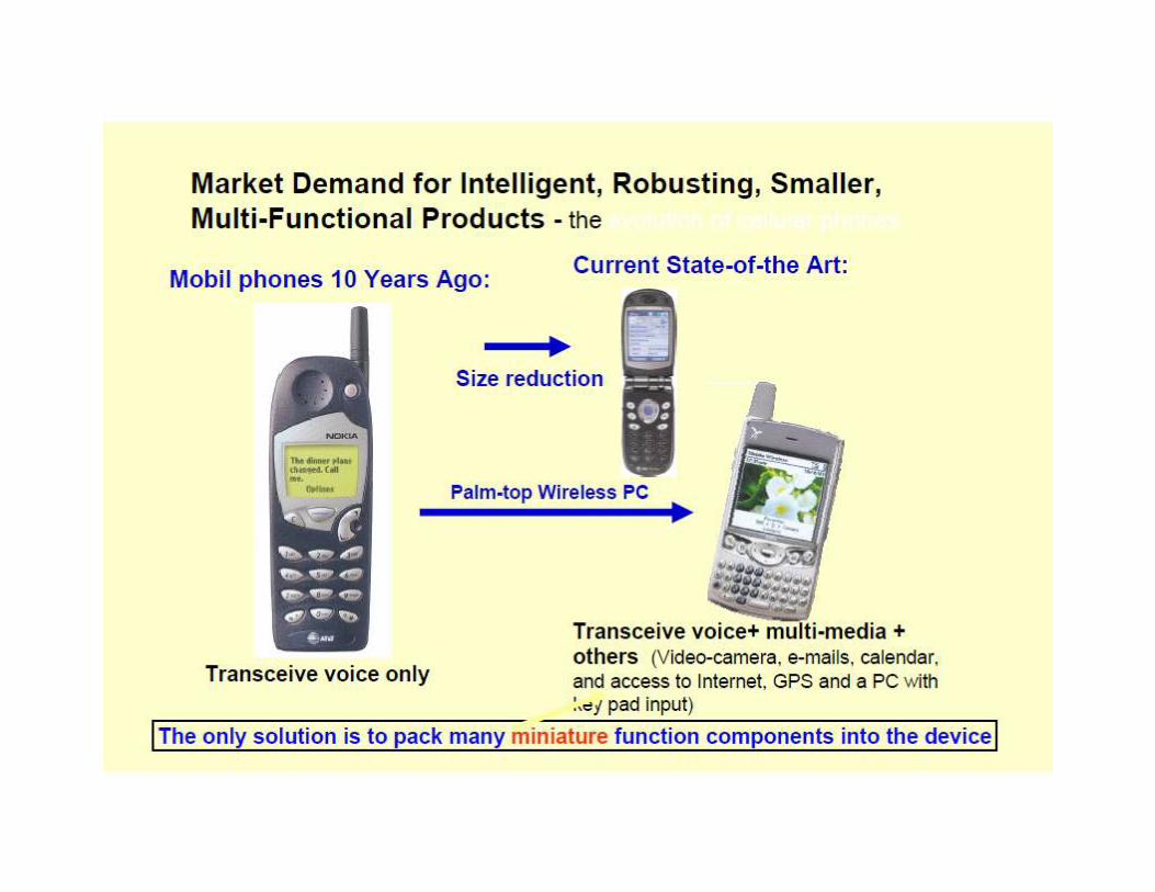
Miniaturization of ComputersMiniaturization of ComputersMiniaturization of ComputersMiniaturization of Computers
http://educationstormfront.wordpre
ss.com/2013/05/17/hardware-
innovation-vs-software-innovation/
http://ccatechnohistory.blogspot.in/2010/09
/evolution-of-computers.html

Ref : Hsu, T.R., L.I., 14, 168-171, 1972

Miniaturization: Information StorageMiniaturization: Information StorageMiniaturization: Information StorageMiniaturization: Information Storage
Fgure Source: International Data Corporation (IDC)
Data recording on a disc
� The information is transformed to strings of binary digits (0s and 1s, also
called bits).
� Each bit is then laser “burned” into the disc, using a single beam of light,
in the form of dots.
� The storage capacity of optical discs is mainly limited by the physical
dimensions of the dots.

Miniaturization: Information StorageMiniaturization: Information StorageMiniaturization: Information StorageMiniaturization: Information Storage
How far can we reduce the size of the dots?
Abbe’s Limit:
If a light beam is focused through a lens,
the diameter of the resulting spot of light
can’t be smaller than half its wavelength.
Way to get around the problem
http://theconversation.com/more-data-
storage-heres-how-to-fit-1-000-terabytes-
on-a-dvd-15306
Way to get around the problem
�The first beam (red, in the figure) has a
round shape, and is used to write data.
� Then, place a doughnut-shaped laser
(purple, in the figure) around the initial
laser in order to limit the abilities of the
first beam. This effectively made the
standard laser’s diameter smaller, and it
could then write smaller bits


ScalingScalingScalingScaling----Surface to Volume Ratio IncreasesSurface to Volume Ratio IncreasesSurface to Volume Ratio IncreasesSurface to Volume Ratio Increases
As surface to volume ratio increases
• A greater amount of a substance
comes in contact with surrounding
material.
• This helps in loading more drugs for
drug delivery.
• Also, elephant and dragonfly
example.


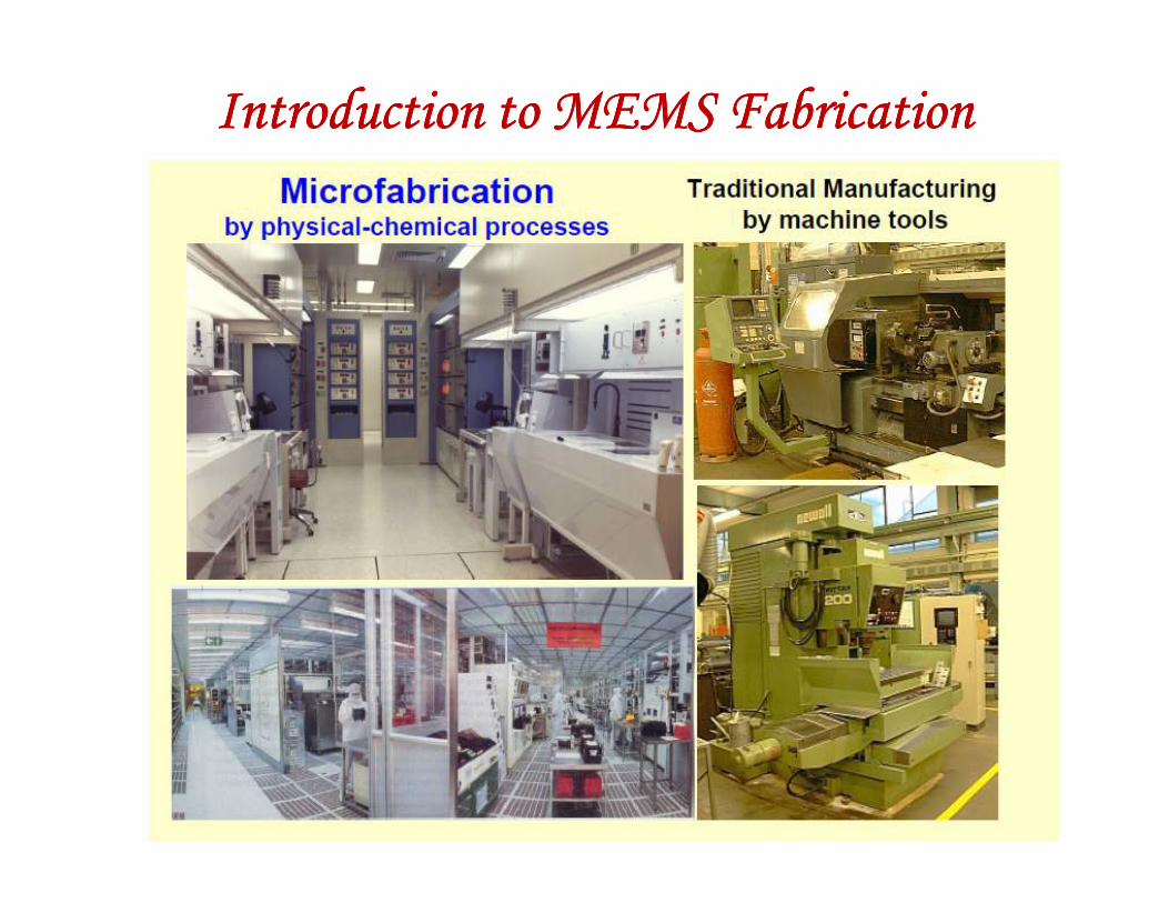
Introduction to MEMS FabricationIntroduction to MEMS FabricationIntroduction to MEMS FabricationIntroduction to MEMS Fabrication
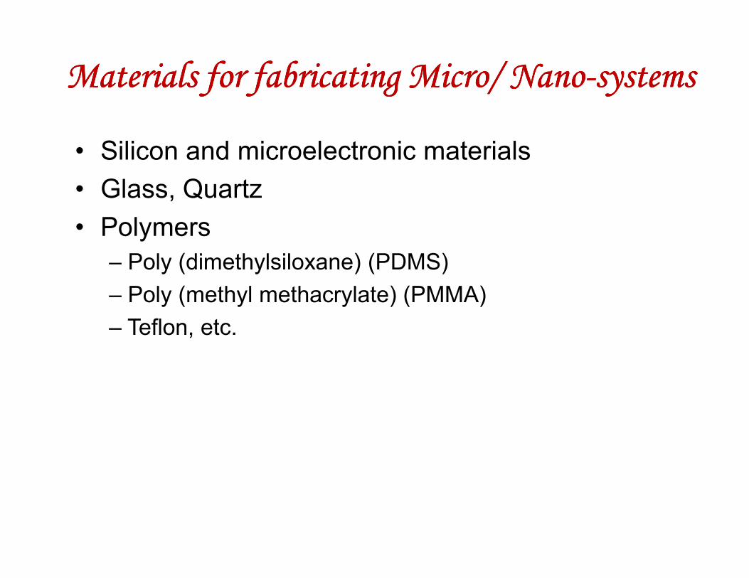
Materials for fabricating Micro/ NanoMaterials for fabricating Micro/ NanoMaterials for fabricating Micro/ NanoMaterials for fabricating Micro/ Nano----systemssystemssystemssystems
• Silicon and microelectronic materials
• Glass, Quartz
• Polymers
– Poly (dimethylsiloxane) (PDMS)
– Poly (methyl methacrylate) (PMMA)– Poly (methyl methacrylate) (PMMA)
– Teflon, etc.

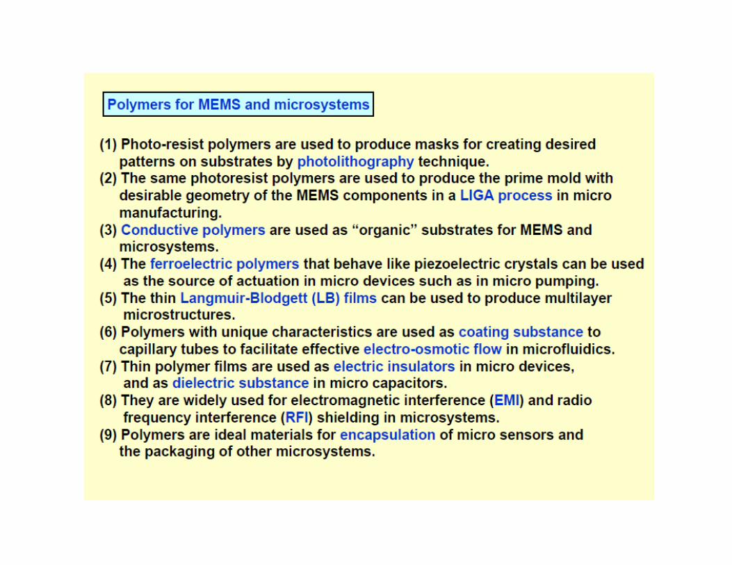
Materials for MEMSMaterials for MEMSMaterials for MEMSMaterials for MEMS


Taxonomy of Taxonomy of Taxonomy of Taxonomy of MicrofabricationMicrofabricationMicrofabricationMicrofabrication ProcessesProcessesProcessesProcesses

Ion ImplantationIon ImplantationIon ImplantationIon Implantation
( )
∆
−−
∆=
2
2
2exp
2)(
p
p
pR
Rx
R
QxN
π

DiffusionDiffusionDiffusionDiffusion
x
xNDF
∂∂
−=)(
Fick’s Law:F: dopant flux
D: diffusion coefficient
N: dopant concentration

Taxonomy of Taxonomy of Taxonomy of Taxonomy of MicrofabricationMicrofabricationMicrofabricationMicrofabrication ProcessesProcessesProcessesProcesses
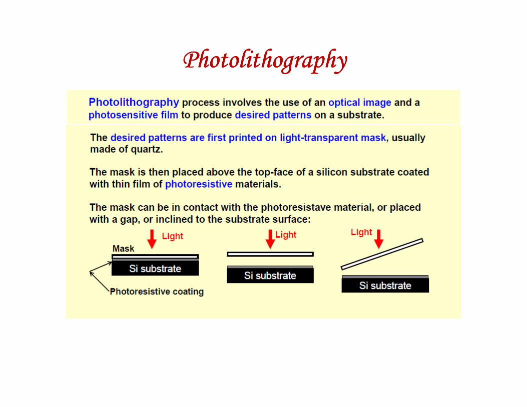
PhotolithographyPhotolithographyPhotolithographyPhotolithography
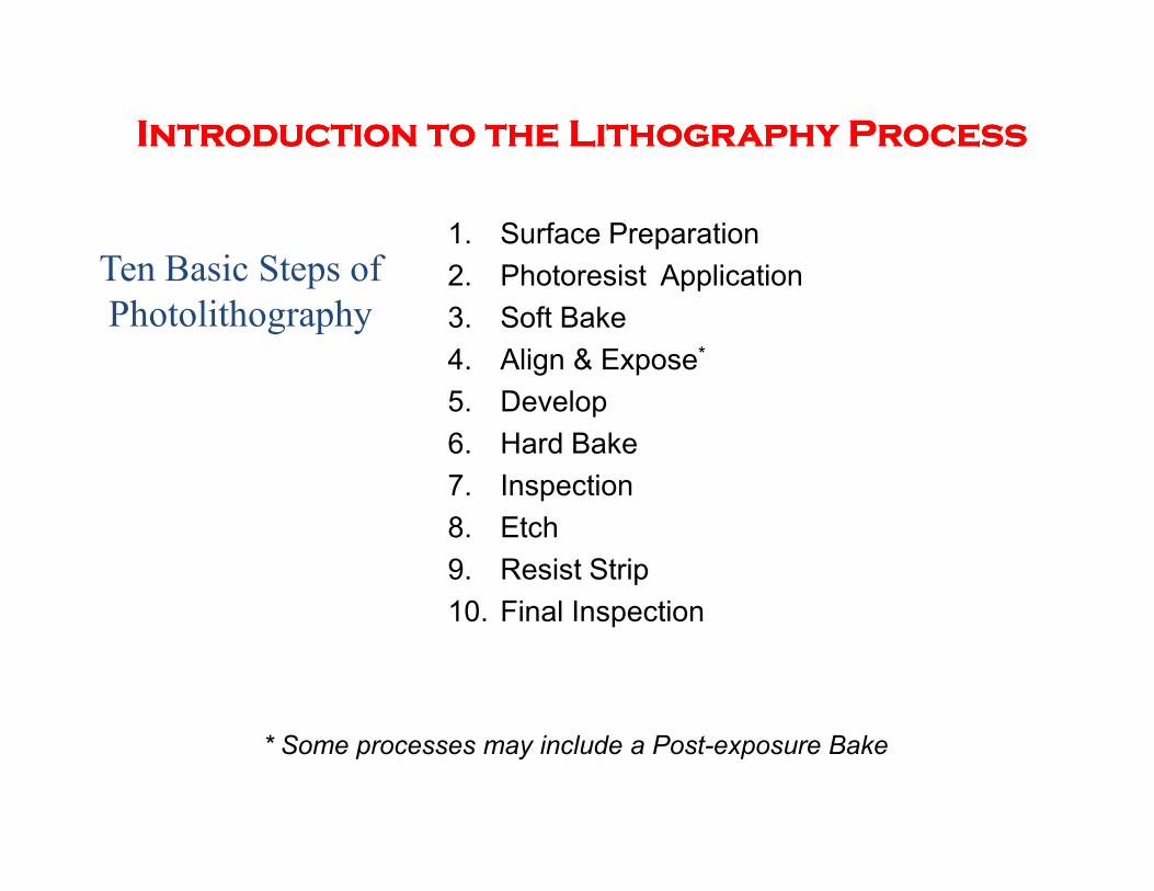
Ten Basic Steps of
Photolithography
1. Surface Preparation
2. Photoresist Application
3. Soft Bake
4. Align & Expose*
5. Develop
6. Hard Bake
Introduction to the Lithography ProcessIntroduction to the Lithography ProcessIntroduction to the Lithography ProcessIntroduction to the Lithography Process
6. Hard Bake
7. Inspection
8. Etch
9. Resist Strip
10. Final Inspection
* Some processes may include a Post-exposure Bake

PhotolithographyPhotolithographyPhotolithographyPhotolithography
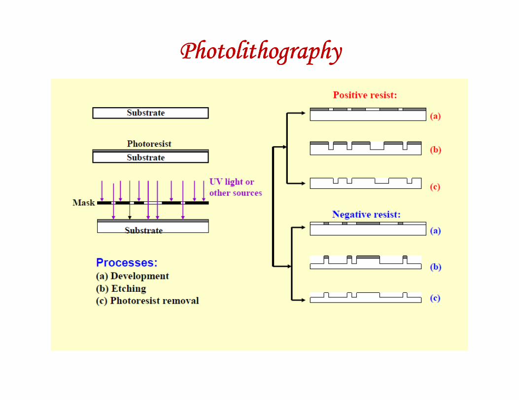
PhotolithographyPhotolithographyPhotolithographyPhotolithography

Negative LithographyNegative LithographyNegative LithographyNegative Lithography
Island
Areas exposed to light become polymerized and resist the develop chemical.
Ultraviolet Light
Exposed area
of photoresist
Chrome island on
glass mask
silicon substrate
oxide
photoresist
Window
Resulting pattern after the resist is developed.
photoresist
oxide
silicon substrate
of photoresist
Shadow on
photoresist

Positive LithographyPositive LithographyPositive LithographyPositive Lithography
Island
Areas exposed to light become photosoluble.
Shadow on
photoresist
Chrome island on
glass mask
Ultraviolet Light
silicon substrate
oxide
photoresist
Window
Resulting pattern after the resist is developed.
photoresist
Exposed area
of photoresist
photoresist
silicon substrate
oxide