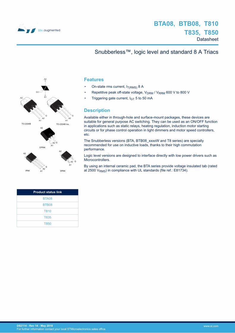
microcontrollers. t835, t850 bta08, btb08, t810 · a2 a1 a2 d²pak to-220ab to-220ab ins. ipak dpak...
TRANSCRIPT
A2
A1A2
D²PAK
TO-220AB TO-220AB Ins.
DPAKIPAK
A2
A1
G
G
A1A2 G
A2
A1
GA2
A2
A2
A2
A1
GA2
A1
G
Features• On-state rms current, IT(RMS) 8 A• Repetitive peak off-state voltage, VDRM / VRRM 600 V to 800 V• Triggering gate current, IGT 5 to 50 mA
DescriptionAvailable either in through-hole and surface-mount packages, these devices aresuitable for general purpose AC switching. They can be used as an ON/OFF functionin applications such as static relays, heating regulation, induction motor startingcircuits or for phase control operation in light dimmers and motor speed controllers,etc.
The Snubberless versions (BTA, BTB08_xxxxW and T8 series) are speciallyrecommended for use on inductive loads, thanks to their high commutationperformance.
Logic level versions are designed to interface directly with low power drivers such asMicrocontrollers.
By using an internal ceramic pad, the BTA series provide voltage insulated tab (ratedat 2500 VRMS) in compliance with UL standards (file ref.: E81734).
Product status link
BTA08
BTB08
T810
T835
T850
Snubberless™, logic level and standard 8 A Triacs
BTA08, BTB08, T810 T835, T850
Datasheet
DS2114 - Rev 14 - May 2018For further information contact your local STMicroelectronics sales office.
www.st.com
1 Characteristics
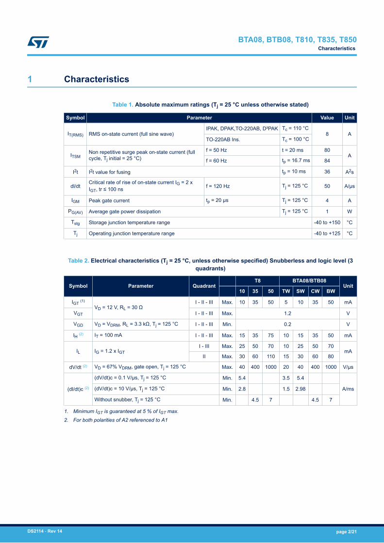
Table 1. Absolute maximum ratings (Tj = 25 °C unless otherwise stated)
Symbol Parameter Value Unit
IT(RMS) RMS on-state current (full sine wave)IPAK, DPAK,TO-220AB, D²PAK Tc = 110 °C
8 ATO-220AB Ins. Tc = 100 °C
ITSMNon repetitive surge peak on-state current (fullcycle, Tj initial = 25 °C)
f = 50 Hz t = 20 ms 80A
f = 60 Hz tp = 16.7 ms 84
I2t I2t value for fusing tp = 10 ms 36 A2s
dl/dtCritical rate of rise of on-state current IG = 2 xIGT, tr ≤ 100 ns f = 120 Hz Tj = 125 °C 50 A/µs
IGM Peak gate current tp = 20 µs Tj = 125 °C 4 A
PG(AV) Average gate power dissipation Tj = 125 °C 1 W
Tstg Storage junction temperature range -40 to +150 °C
Tj Operating junction temperature range -40 to +125 °C
Table 2. Electrical characteristics (Tj = 25 °C, unless otherwise specified) Snubberless and logic level (3quadrants)
Symbol Parameter QuadrantT8 BTA08/BTB08
Unit10 35 50 TW SW CW BW
IGT (1)
VD = 12 V, RL = 30 ΩI - II - III Max. 10 35 50 5 10 35 50 mA
VGT I - II - III Max. 1.2 V
VGD VD = VDRM, RL = 3.3 kΩ, Tj = 125 °C I - II - III Min. 0.2 V
IH (2) IT = 100 mA I - II - III Max. 15 35 75 10 15 35 50 mA
IL IG = 1.2 x IGTI - III Max. 25 50 70 10 25 50 70
mAII Max. 30 60 110 15 30 60 80
dV/dt (2) VD = 67% VDRM, gate open, Tj = 125 °C Max. 40 400 1000 20 40 400 1000 V/µs
(dl/dt)c (2)
(dV/dt)c = 0.1 V/µs, Tj = 125 °C Min. 5.4 3.5 5.4
A/ms(dV/dt)c = 10 V/µs, Tj = 125 °C Min. 2.8 1.5 2.98
Without snubber, Tj = 125 °C Min. 4.5 7 4.5 7
1. Minimum IGT is guaranteed at 5 % of IGT max.
2. For both polarities of A2 referenced to A1
BTA08, BTB08, T810, T835, T850Characteristics
DS2114 - Rev 14 page 2/21
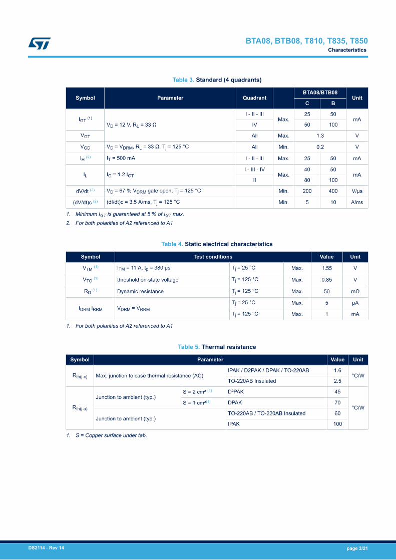
Table 3. Standard (4 quadrants)
Symbol Parameter QuadrantBTA08/BTB08
UnitC B
IGT (1)
VD = 12 V, RL = 33 Ω
I - II - IIIMax.
25 50mA
IV 50 100
VGT All Max. 1.3 V
VGD VD = VDRM, RL = 33 Ω, Tj = 125 °C All Min. 0.2 V
IH (2) IT = 500 mA I - II - III Max. 25 50 mA
IL IG = 1.2 IGTI - III - IV
Max.40 50
mAII 80 100
dV/dt (2) VD = 67 % VDRM gate open, Tj = 125 °C Min. 200 400 V/µs
(dV/dt)c (2) (dI/dt)c = 3.5 A/ms, Tj = 125 °C Min. 5 10 A/ms
1. Minimum IGT is guaranteed at 5 % of IGT max.
2. For both polarities of A2 referenced to A1
Table 4. Static electrical characteristics
Symbol Test conditions Value Unit
VTM (1) ITM = 11 A, tp = 380 µs Tj = 25 °C Max. 1.55 V
VTO (1) threshold on-state voltage Tj = 125 °C Max. 0.85 V
RD (1) Dynamic resistance Tj = 125 °C Max. 50 mΩ
IDRM IRRM VDRM = VRRMTj = 25 °C Max. 5 µA
Tj = 125 °C Max. 1 mA
1. For both polarities of A2 referenced to A1
Table 5. Thermal resistance
Symbol Parameter Value Unit
Rth(j-c) Max. junction to case thermal resistance (AC)IPAK / D2PAK / DPAK / TO-220AB 1.6
°C/WTO-220AB Insulated 2.5
Rth(j-a)
Junction to ambient (typ.)S = 2 cm² (1) D²PAK 45
°C/WS = 1 cm²(1) DPAK 70
Junction to ambient (typ.)TO-220AB / TO-220AB Insulated 60
IPAK 100
1. S = Copper surface under tab.
BTA08, BTB08, T810, T835, T850Characteristics
DS2114 - Rev 14 page 3/21
1.1 Characteristics (curves)
Figure 1. Maximum power dissipation versus on-stateRMS current (full cycle)
0 1 2 3 4 5 6 7 80
1
2
3
4
5
6
7
8
9
10P(W)
IT(RMS)(A)
Figure 2. RMS on-state current versus temperature (fullcycle)
0 25 50 75 100 1250
1
2
3
4
5
6
7
8
9
10IT(RMS)(A)
Tc(°C)
BTB/T8
BTA
Figure 3. RMS on-state current versus ambienttemperature (full cycle)
0 25 50 75 100 1250.0
0.5
1.0
1.5
2.0
2.5
3.0
3.5IT(RMS)(A)
Tc(°C)
Printed circuit board FR4, copper thickness: 35 µmD²PAK(S = 1 cm²)
DPAK(S = 0.5 cm²)
Figure 4. Relative variation of thermal impedance versuspulse duration
1E-3 1E-2 1E-1 1E+0 1E+1 1E+2 5E+21E-3
1E-2
1E-1
1E+0
K = [Zth/Rth]
tp(s)
Zth(j-c)
DPAK/IPAKZth(j-a)
TO-220AB/D²PAKZth(j-a)
BTA08, BTB08, T810, T835, T850Characteristics (curves)
DS2114 - Rev 14 page 4/21
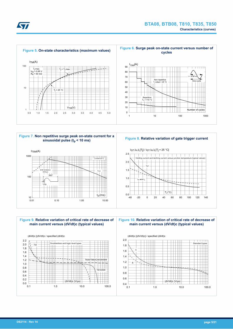
Figure 5. On-state characteristics (maximum values)
0.5 1.0 1.5 2.0 2.5 3.0 3.5 4.0 4.5 5.01
10
100
ITM(A)
VTM(V)
Tj max.Vto = 0.85 VRd = 50 mΩ
Tj = Tj max.
Tj = 25 °C
Figure 6. Surge peak on-state current versus number ofcycles
0
10
20
30
40
50
60
70
80
90
1 10 100 1000
Number of cycles
ITSM(A)
Non repetitiveTj initial = 25 °C
RepetitiveTC = 110 °C
One cycle
t = 16.66 ms
Figure 7. Non repetitive surge peak on-state current for asinusoidal pulse (tp < 10 ms)
0.01 0.10 1.00 10.0010
100
1000
t (ms)p
T initial=25°Cj
ITSMdI/dt limitation:
50A/µs
360°
α
ITSM(A)
Figure 8. Relative variation of gate trigger current
-40 -20 0 20 40 60 80 100 120 1400.0
0.5
1.0
1.5
2.0
2.5IGT,IH,IL[Tj] / IGT,IH,IL[Tj = 25 °C]
Tj (°C)
IH and IL
IGT
Holding current and latching current versus junction temperature (typical values)
Figure 9. Relative variation of critical rate of decrease ofmain current versus (dV/dt)c (typical values)
0.1 1.0 10.0 100.00.00.20.40.60.81.01.21.41.61.82.02.2
(dl/dt)c [(dV/dt)c / specified (dl/dt)c
(dV/dt)c (V/µs)
T810/SW
TW
T835/T850/CW/SW/BW
Snubberless and logic level types
Figure 10. Relative variation of critical rate of decrease ofmain current versus (dV/dt)c (typical values)
0.1 1.0 10.0 100.00.4
0.6
0.8
1.0
1.2
1.4
1.6
1.8
2.0(dl/dt)c [(dV/dt)c] / specified (dl/dt)c
(dV/dt)c (V/µs)
C
Standard types
B
BTA08, BTB08, T810, T835, T850Characteristics (curves)
DS2114 - Rev 14 page 5/21
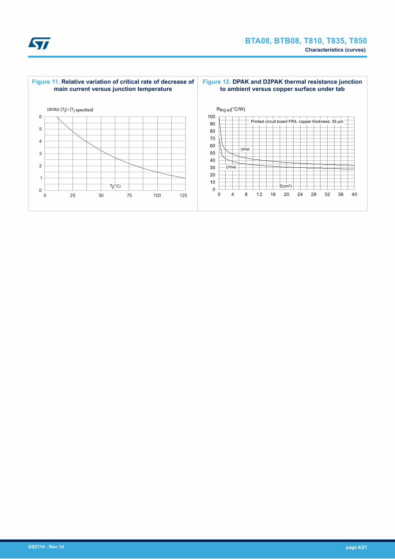
Figure 11. Relative variation of critical rate of decrease ofmain current versus junction temperature
0 25 50 75 100 1250
1
2
3
4
5
6(dl/dt)c [Tj] / [Tj specified]
Tj(°C)
Figure 12. DPAK and D2PAK thermal resistance junctionto ambient versus copper surface under tab
0 4 8 12 16 20 24 28 32 36 400
102030405060708090
100Rth(j-a)(°C/W)
S(cm²)
Printed circuit board FR4, copper thickness: 35 µm
DPAK
D²PAK
BTA08, BTB08, T810, T835, T850Characteristics (curves)
DS2114 - Rev 14 page 6/21
2 Package information
In order to meet environmental requirements, ST offers these devices in different grades of ECOPACK®
packages, depending on their level of environmental compliance. ECOPACK® specifications, grade definitionsand product status are available at: www.st.com. ECOPACK® is an ST trademark.
BTA08, BTB08, T810, T835, T850Package information
DS2114 - Rev 14 page 7/21
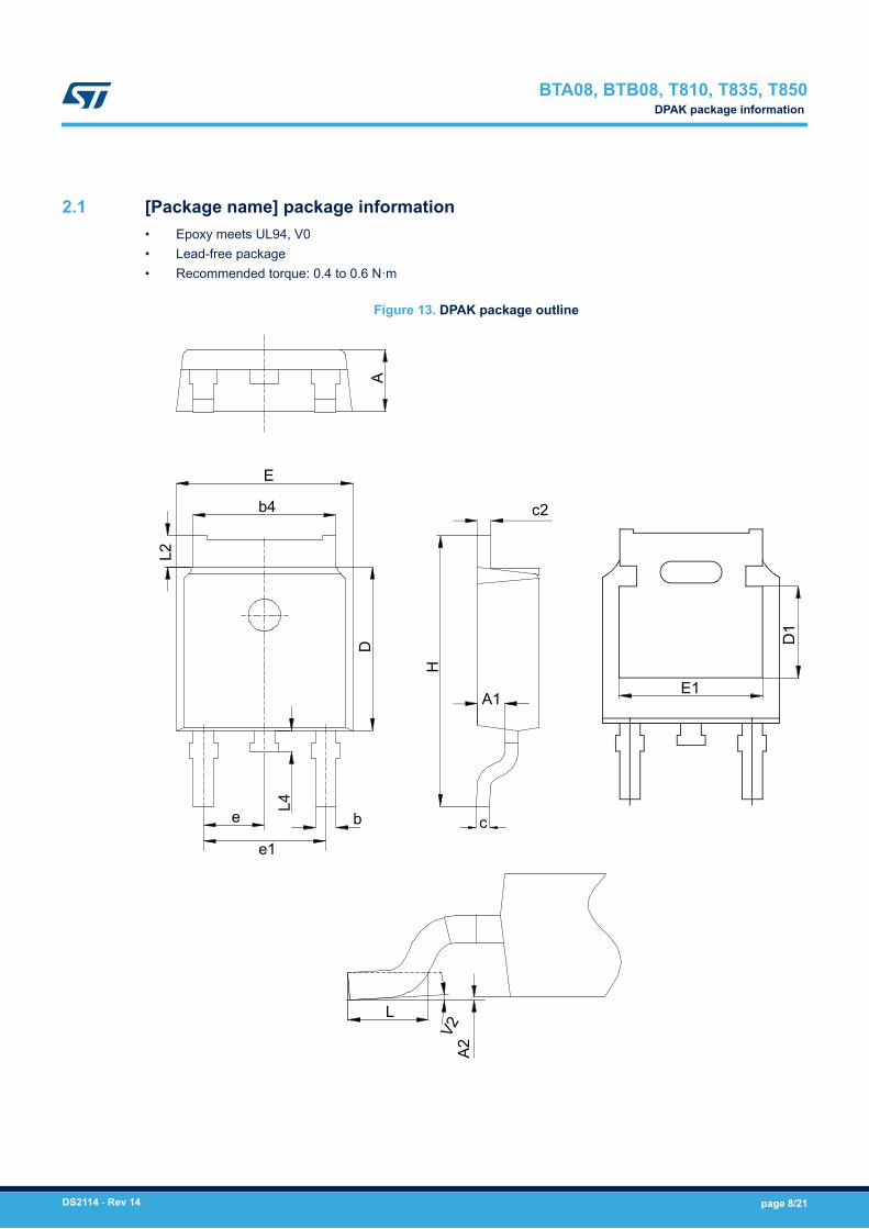
2.1 [Package name] package information• Epoxy meets UL94, V0• Lead-free package• Recommended torque: 0.4 to 0.6 N·m
Figure 13. DPAK package outline
A
E
b4
2L
D
4L
e
e1
b c
A1
H
c2
L
V2A2
E1
D1
BTA08, BTB08, T810, T835, T850DPAK package information
DS2114 - Rev 14 page 8/21

Table 6. DPAK package mechanical data
Ref.
Dimensions
Millimeters Inches(1)
Min. Typ. Max. Min. Typ. Max.
A 2.18 2.40 0.0858 0.0945
A1 0.90 1.10 0.0354 0.0433
A2 0.03 0.23 0.0012 0.0091
b 0.64 0.90 0.0252 0.354
b4 4.95 5.46 0.1949 0.2150
c 0.46 0.61 0.0181 0.0240
c2 0.46 0.60 0.0181 0.0236
D 5.97 6.22 0.2350 0.2449
D1 5.10 0.2008
E 6.35 6.73 0.2500 0.2650
E1 4.32 0.1701
e 2.29 0.0900
e1 4.57 0.1800
H 9.35 10.40 0.3681 0.4094
L 1.00 1.78 0.0394 0.0701
L2 1.27 0.0500
L4 0.60 1.02 0.0236 0.0402
V2 0° +8° 0° +8°
1. Dimensions in inches are given for reference only
Note: This package drawing may slightly differ from the physical package. However, all the specified dimensions areguaranteed.
Figure 14. DPAK recommended footprint (dimensions are in mm)
6.7
6.7 3.03.0
1.6
4.572A
B
The device must be positioned within 0.05 AB
12.7
BTA08, BTB08, T810, T835, T850DPAK package information
DS2114 - Rev 14 page 9/21
2.2 IPAK package information
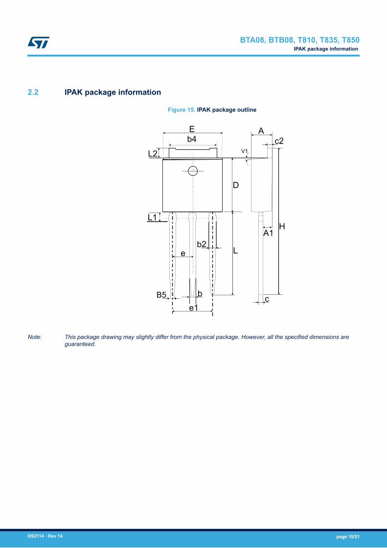
Figure 15. IPAK package outline
D
V1
Ac2
H
Lb2
A1
e1
e
b c
L2
L1
Eb4
B5
Note: This package drawing may slightly differ from the physical package. However, all the specified dimensions areguaranteed.
BTA08, BTB08, T810, T835, T850IPAK package information
DS2114 - Rev 14 page 10/21
Table 7. IPAK package mechanical data
Ref.
Dimensions
Millimeters Inches(1)
Min. Typ. Max. Min. Typ. Max.
A 2.20 2.40 0.0866 0.0945
A1 0.90 1.10 0.0354 0.0433
b 0.64 0.90 0.0252 0.0354
b2 0.95 0.0374
b4 5.20 5.43 0.2047 0.2138
B5 0.30 0.0118
c 0.45 0.60 0.0177 0.0236
c2 0.46 0.60 0.0181 0.0236
D 6.00 6.20 0.2362 0.2441
E 6.40 6.65 0.2520 0.2618
e 2.28 0.0898
e1 4.40 4.60 0.1732 0.1811
H 16.10 0.6339
L 9.00 9.60 0.3545 0.3780
L1 0.80 1.20 0.0315 0.0472
L2 0.80 1.25 0.0315 0.0492
V1 10° 10°
1. Inch dimensions are for reference only.
BTA08, BTB08, T810, T835, T850IPAK package information
DS2114 - Rev 14 page 11/21
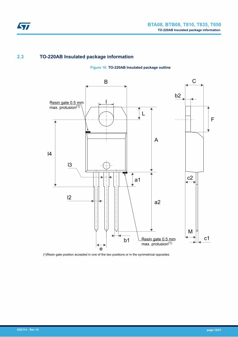
2.3 TO-220AB Insulated package information
Figure 16. TO-220AB Insulated package outline
C
b2
c2
FL
A
a1
a2
B
eb1
I4
l3
l2
c1M
Resin gate 0.5 mmmax. protusion(1)
Resin gate 0.5 mmmax. protusion(1)
(1)Resin gate position accepted in one of the two positions or in the symmetrical opposites.
I
BTA08, BTB08, T810, T835, T850TO-220AB Insulated package information
DS2114 - Rev 14 page 12/21
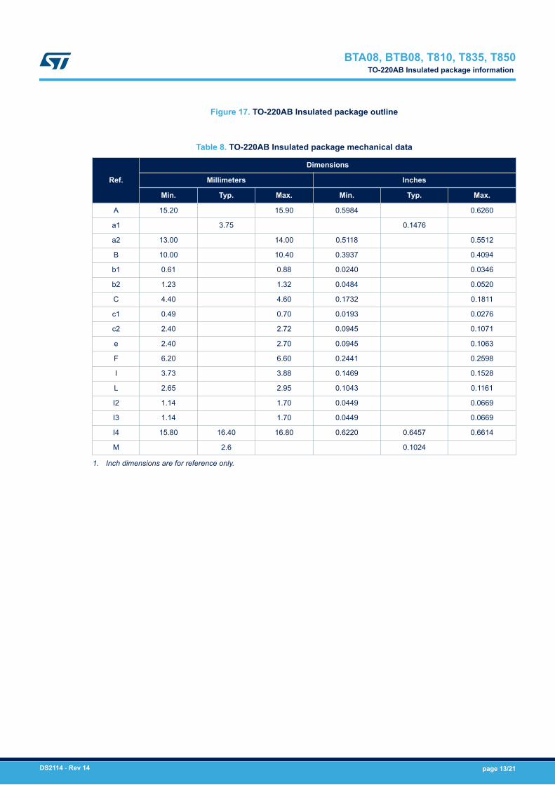
Figure 17. TO-220AB Insulated package outline
Table 8. TO-220AB Insulated package mechanical data
Ref.
Dimensions
Millimeters Inches
Min. Typ. Max. Min. Typ. Max.
A 15.20 15.90 0.5984 0.6260
a1 3.75 0.1476
a2 13.00 14.00 0.5118 0.5512
B 10.00 10.40 0.3937 0.4094
b1 0.61 0.88 0.0240 0.0346
b2 1.23 1.32 0.0484 0.0520
C 4.40 4.60 0.1732 0.1811
c1 0.49 0.70 0.0193 0.0276
c2 2.40 2.72 0.0945 0.1071
e 2.40 2.70 0.0945 0.1063
F 6.20 6.60 0.2441 0.2598
I 3.73 3.88 0.1469 0.1528
L 2.65 2.95 0.1043 0.1161
I2 1.14 1.70 0.0449 0.0669
I3 1.14 1.70 0.0449 0.0669
I4 15.80 16.40 16.80 0.6220 0.6457 0.6614
M 2.6 0.1024
1. Inch dimensions are for reference only.
BTA08, BTB08, T810, T835, T850TO-220AB Insulated package information
DS2114 - Rev 14 page 13/21
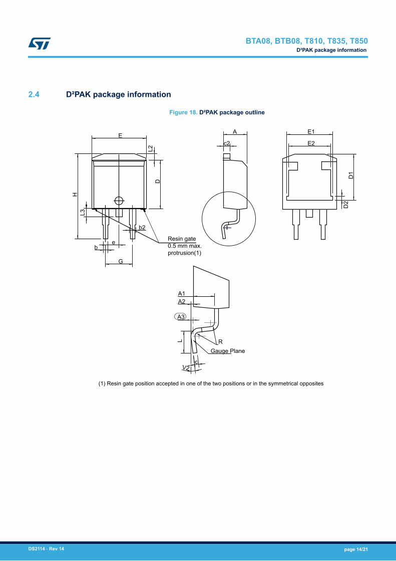
2.4 D²PAK package information
Figure 18. D²PAK package outline
(1) Resin gate position accepted in one of the two positions or in the symmetrical opposites
e
G
E1
E2c2
A
D2
D1
b
b2
H
E
L2
L3
D
V2c
A1A2
A3
L RGauge Plane
Resin gate0.5 mm max.protrusion(1)
BTA08, BTB08, T810, T835, T850D²PAK package information
DS2114 - Rev 14 page 14/21
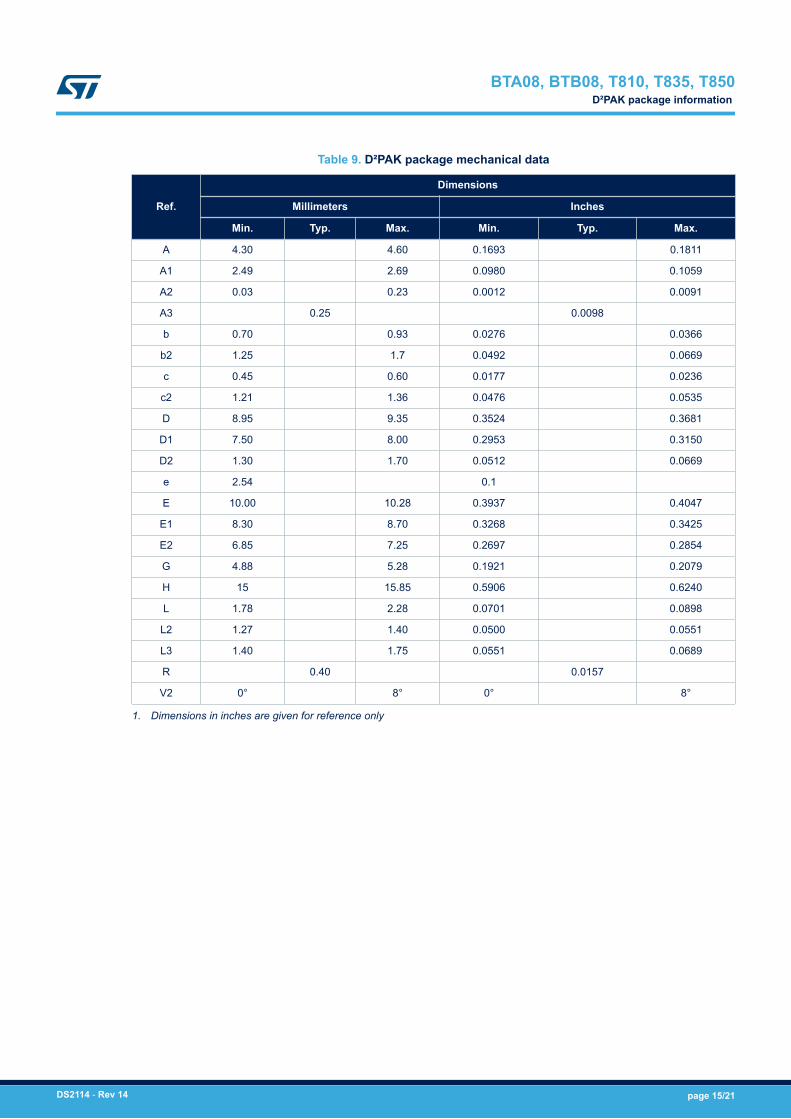
Table 9. D²PAK package mechanical data
Ref.
Dimensions
Millimeters Inches
Min. Typ. Max. Min. Typ. Max.
A 4.30 4.60 0.1693 0.1811
A1 2.49 2.69 0.0980 0.1059
A2 0.03 0.23 0.0012 0.0091
A3 0.25 0.0098
b 0.70 0.93 0.0276 0.0366
b2 1.25 1.7 0.0492 0.0669
c 0.45 0.60 0.0177 0.0236
c2 1.21 1.36 0.0476 0.0535
D 8.95 9.35 0.3524 0.3681
D1 7.50 8.00 0.2953 0.3150
D2 1.30 1.70 0.0512 0.0669
e 2.54 0.1
E 10.00 10.28 0.3937 0.4047
E1 8.30 8.70 0.3268 0.3425
E2 6.85 7.25 0.2697 0.2854
G 4.88 5.28 0.1921 0.2079
H 15 15.85 0.5906 0.6240
L 1.78 2.28 0.0701 0.0898
L2 1.27 1.40 0.0500 0.0551
L3 1.40 1.75 0.0551 0.0689
R 0.40 0.0157
V2 0° 8° 0° 8°
1. Dimensions in inches are given for reference only
BTA08, BTB08, T810, T835, T850D²PAK package information
DS2114 - Rev 14 page 15/21
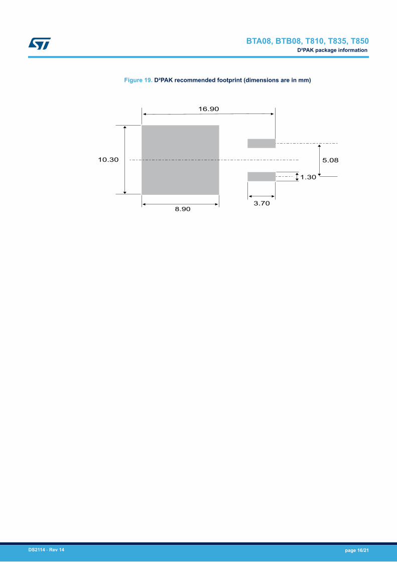
Figure 19. D²PAK recommended footprint (dimensions are in mm)
16.90
10.30
3.70
5.08
1.30
8.90
BTA08, BTB08, T810, T835, T850D²PAK package information
DS2114 - Rev 14 page 16/21
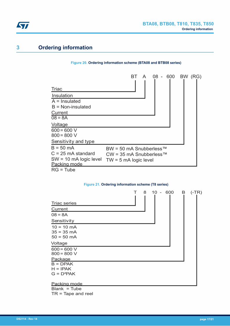
3 Ordering information
Figure 20. Ordering information scheme (BTA08 and BTB08 series)
BT A 08 - 600 BW (RG)
Triac InsulationA = InsulatedB = Non-insulatedCurrent
Voltage
Sensitivity and type
Packing modeRG = Tube
08 = 8A
600 = 600 V800 = 800 V
B = 50 mAC = 25 mA standardSW = 10 mA logic level
BW = 50 mA Snubberless™ CW = 35 mA Snubberless™ TW = 5 mA logic level
Figure 21. Ordering information scheme (T8 series)
T 8 10 - 600 B (-TR)
Triac series
PackageB = DPAKH = IPAKG = D²PAK
Current
Voltage
Sensitivity
Packing modeBlank = TubeTR = Tape and reel
08 = 8A
600 = 600 V800 = 800 V
10 = 10 mA35 = 35 mA50 = 50 mA
BTA08, BTB08, T810, T835, T850Ordering information
DS2114 - Rev 14 page 17/21
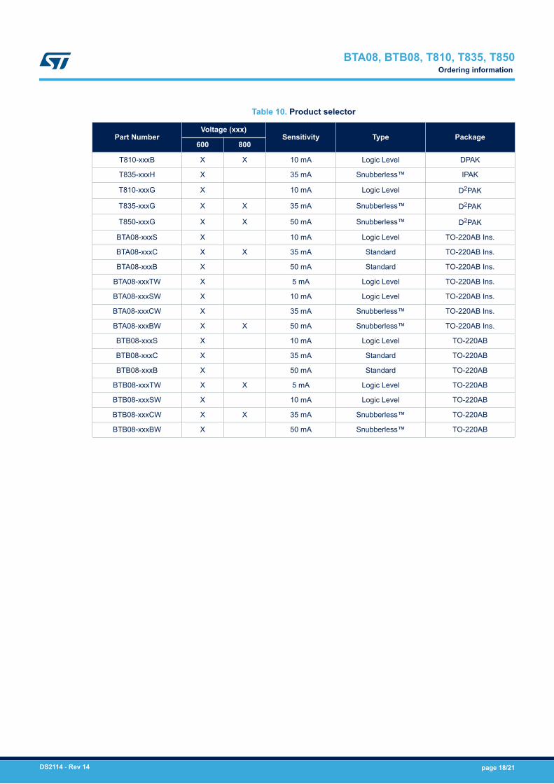
Table 10. Product selector
Part NumberVoltage (xxx)
Sensitivity Type Package600 800
T810-xxxB X X 10 mA Logic Level DPAK
T835-xxxH X 35 mA Snubberless™ IPAK
T810-xxxG X 10 mA Logic Level D2PAK
T835-xxxG X X 35 mA Snubberless™ D2PAK
T850-xxxG X X 50 mA Snubberless™ D2PAK
BTA08-xxxS X 10 mA Logic Level TO-220AB Ins.
BTA08-xxxC X X 35 mA Standard TO-220AB Ins.
BTA08-xxxB X 50 mA Standard TO-220AB Ins.
BTA08-xxxTW X 5 mA Logic Level TO-220AB Ins.
BTA08-xxxSW X 10 mA Logic Level TO-220AB Ins.
BTA08-xxxCW X 35 mA Snubberless™ TO-220AB Ins.
BTA08-xxxBW X X 50 mA Snubberless™ TO-220AB Ins.
BTB08-xxxS X 10 mA Logic Level TO-220AB
BTB08-xxxC X 35 mA Standard TO-220AB
BTB08-xxxB X 50 mA Standard TO-220AB
BTB08-xxxTW X X 5 mA Logic Level TO-220AB
BTB08-xxxSW X 10 mA Logic Level TO-220AB
BTB08-xxxCW X X 35 mA Snubberless™ TO-220AB
BTB08-xxxBW X 50 mA Snubberless™ TO-220AB
BTA08, BTB08, T810, T835, T850Ordering information
DS2114 - Rev 14 page 18/21
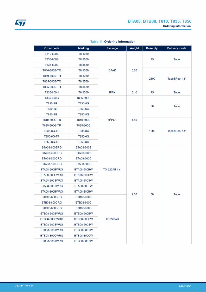
Table 11. Ordering information
Order code Marking Package Weight Base qty. Delivery mode
T810-600B T8 1060
DPAK 0.30
75 TubeT835-600B T8 3560
T835-800B T8 3580
T810-600B-TR T8 1060
2500 Tape&Reel 13"T810-800B-TR T8 1080
T835-600B-TR T8 3560
T835-800B-TR T8 3580
T835-600H T8 3560 IPAK 0.40 75 Tube
T835-600G T835-600G
D2PAK 1.50
50 TubeT835-8G T835-8G
T850-6G T850-6G
T850-8G T850-8G
T810-600G-TR T810-600G
1000 Tape&Reel 13"
T835-600G-TR T835-600G
T835-8G-TR T835-8G
T850-6G-TR T850-6G
T850-8G-TR T850-8G
BTA08-600SRG BTA08-600S
TO-220AB Ins.
2.30 50 Tube
BTA08-600BRG BTA08-600B
BTA08-600CRG BTA08-600C
BTA08-800CRG BTA08-800C
BTA08-600BWRG BTA08-600BW
BTA08-600CWRG BTA08-600CW
BTA08-600SWRG BTA08-600SW
BTA08-600TWRG BTA08-600TW
BTA08-800BWRG BTA08-800BW
BTB08-600BRG BTB08-600B
TO-220AB
BTB08-600CRG BTB08-600C
BTB08-600SRG BTB08-600S
BTB08-600BWRG BTB08-600BW
BTB08-600CWRG BTB08-600CW
BTB08-600SWRG BTB08-600SW
BTB08-600TWRG BTB08-600TW
BTB08-800CWRG BTB08-800CW
BTB08-800TWRG BTB08-800TW
BTA08, BTB08, T810, T835, T850Ordering information
DS2114 - Rev 14 page 19/21
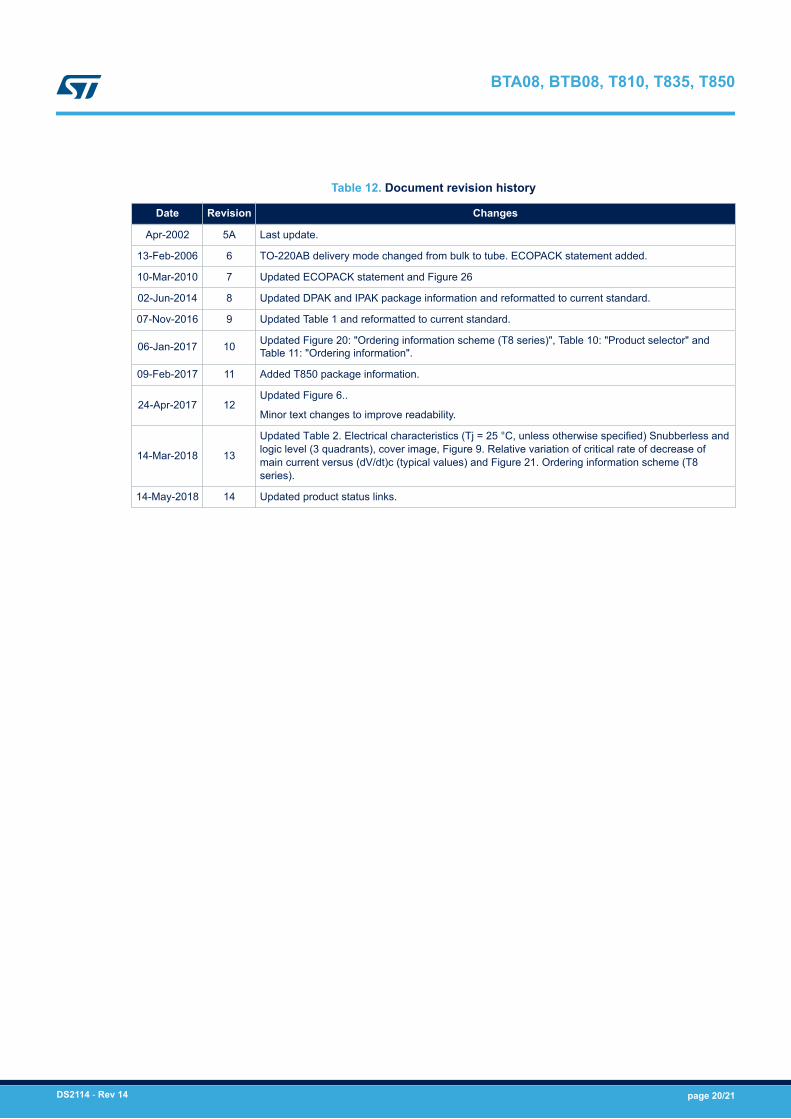
Table 12. Document revision history
Date Revision Changes
Apr-2002 5A Last update.
13-Feb-2006 6 TO-220AB delivery mode changed from bulk to tube. ECOPACK statement added.
10-Mar-2010 7 Updated ECOPACK statement and Figure 26
02-Jun-2014 8 Updated DPAK and IPAK package information and reformatted to current standard.
07-Nov-2016 9 Updated Table 1 and reformatted to current standard.
06-Jan-2017 10 Updated Figure 20: "Ordering information scheme (T8 series)", Table 10: "Product selector" andTable 11: "Ordering information".
09-Feb-2017 11 Added T850 package information.
24-Apr-2017 12Updated Figure 6..
Minor text changes to improve readability.
14-Mar-2018 13
Updated Table 2. Electrical characteristics (Tj = 25 °C, unless otherwise specified) Snubberless and logic level (3 quadrants), cover image, Figure 9. Relative variation of critical rate of decrease of main current versus (dV/dt)c (typical values) and Figure 21. Ordering information scheme (T8 series).
14-May-2018 14 Updated product status links.
BTA08, BTB08, T810, T835, T850
DS2114 - Rev 14 page 20/21
IMPORTANT NOTICE – PLEASE READ CAREFULLY
STMicroelectronics NV and its subsidiaries (“ST”) reserve the right to make changes, corrections, enhancements, modifications, and improvements to STproducts and/or to this document at any time without notice. Purchasers should obtain the latest relevant information on ST products before placing orders. STproducts are sold pursuant to ST’s terms and conditions of sale in place at the time of order acknowledgement.
Purchasers are solely responsible for the choice, selection, and use of ST products and ST assumes no liability for application assistance or the design ofPurchasers’ products.
No license, express or implied, to any intellectual property right is granted by ST herein.
Resale of ST products with provisions different from the information set forth herein shall void any warranty granted by ST for such product.
ST and the ST logo are trademarks of ST. All other product or service names are the property of their respective owners.
Information in this document supersedes and replaces information previously supplied in any prior versions of this document.
© 2018 STMicroelectronics – All rights reserved
BTA08, BTB08, T810, T835, T850
DS2114 - Rev 14 page 21/21