microcontrollers 8051. what is a microcontroller? all of the components needed for a controller were...
TRANSCRIPT

MICROCONTROLLERS8051
WHAT IS A MICROCONTROLLER?
• All of the components needed for a controller were built right onto one chip.
• A microcontroller is a highly integrated chip which includes, on one chip, all or most of the parts needed for a controller.
• The microcontroller could be called a "one-chip solution".
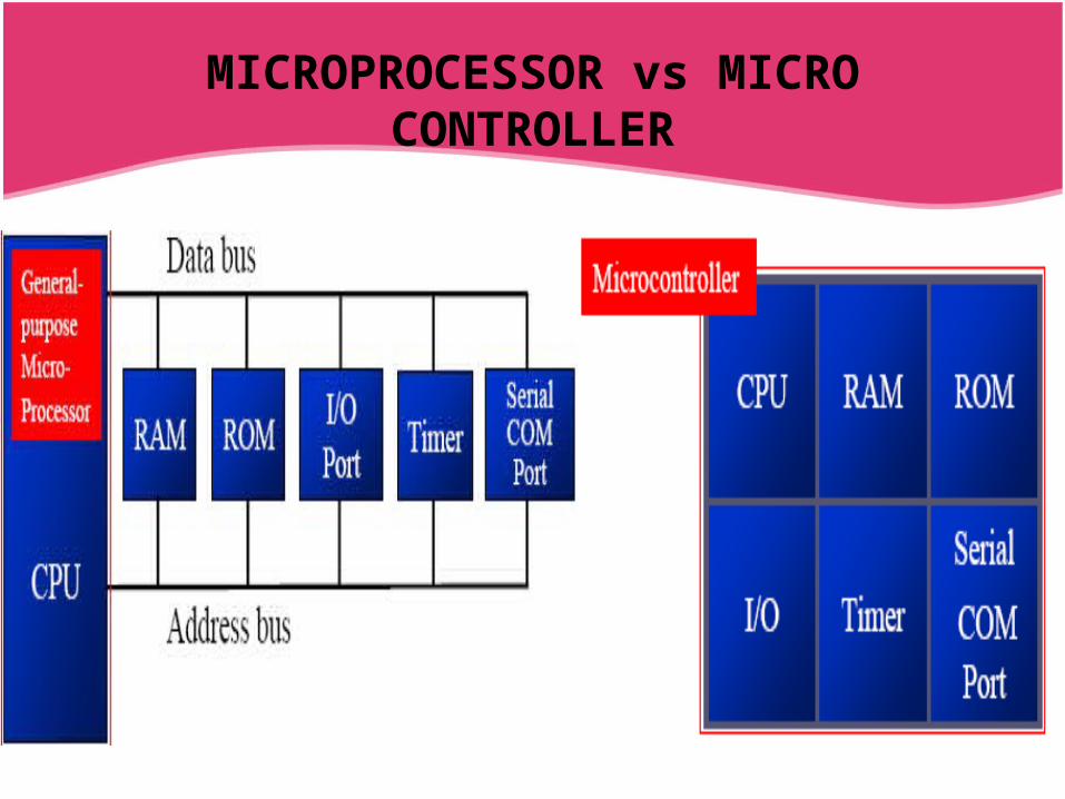
MICROPROCESSOR vs MICRO CONTROLLER
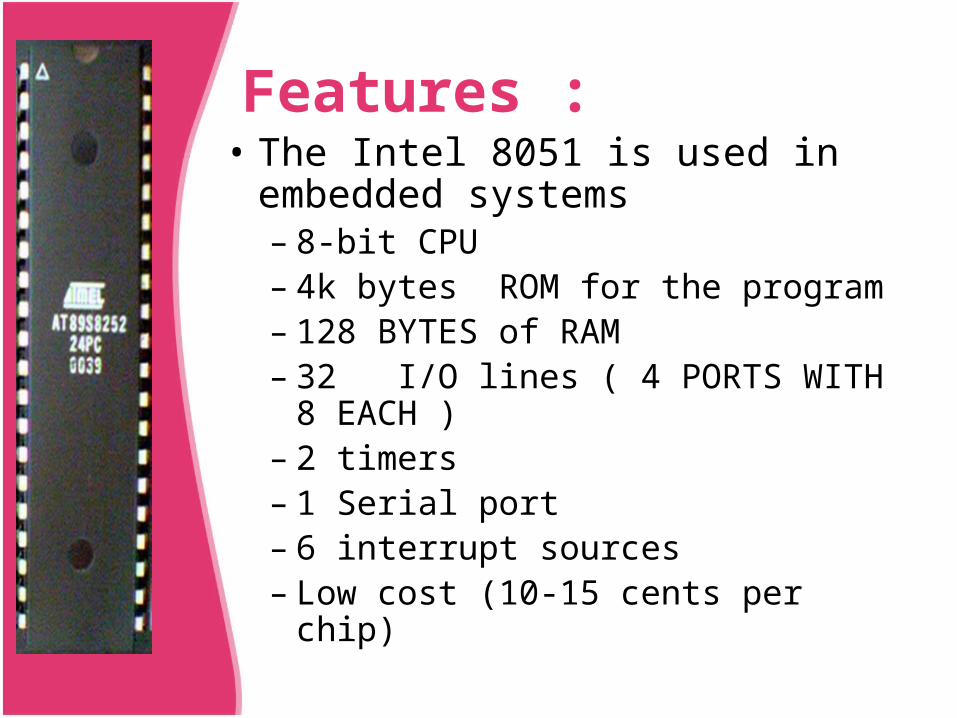
Features :• The Intel 8051 is used in embedded
systems– 8-bit CPU– 4k bytes ROM for the program– 128 BYTES of RAM– 32 I/O lines ( 4 PORTS WITH 8 EACH )– 2 timers– 1 Serial port– 6 interrupt sources– Low cost (10-15 cents per chip)

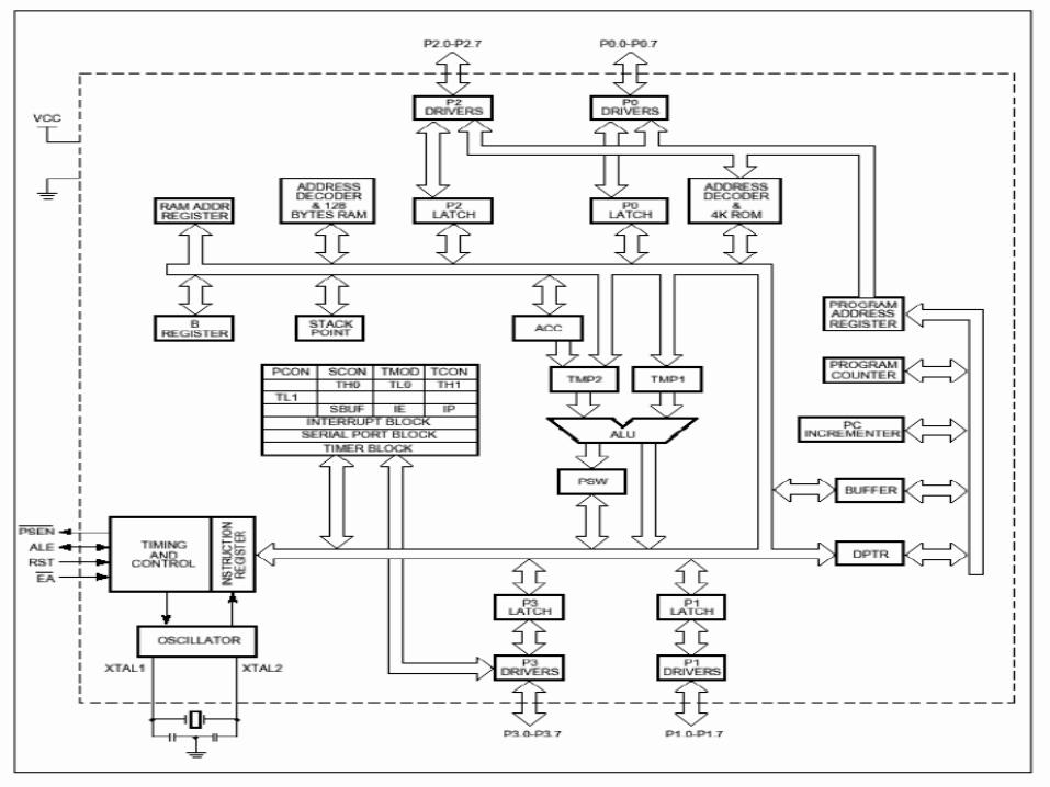
Block Diagram
CPU
InterruptControl
OSC BusControl
4kROM
Timer 1Timer 2
Serial
128 bytes RAM
4 I/O Ports
TXD RXD
External Interrupts
P0 P2 P1 P3Addr/Data

8051 – PIN DIAGRAM
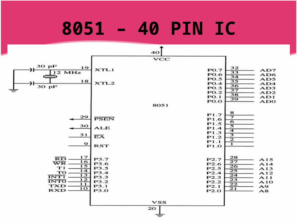
8051 – 40 PIN IC

• 8051 contains four I/O ports (P0 - P3)• Each port can be used as input or output
(bi-direction)

PORT 3 – MULTIPLE FUNCTIONS

IMPORTANT PINS
• PSENPSEN (out): (out): PProgram rogram SStore tore EnEnable, the read signal for able, the read signal for external program memory (active low).external program memory (active low).
• ALEALE (out): (out): AAddress ddress LLatch atch EEnable, to latch address nable, to latch address outputs at Port0 and Port2outputs at Port0 and Port2
• EAEA (in): (in): EExternal xternal AAccess Enable, active low to access ccess Enable, active low to access external program memory locations 0 to 4K external program memory locations 0 to 4K
• RXDRXD,,TXDTXD: UART pins for serial I/O on Port 3: UART pins for serial I/O on Port 3
• XTAL1XTAL1 & & XTAL2XTAL2: Crystal inputs for internal oscillator.: Crystal inputs for internal oscillator.
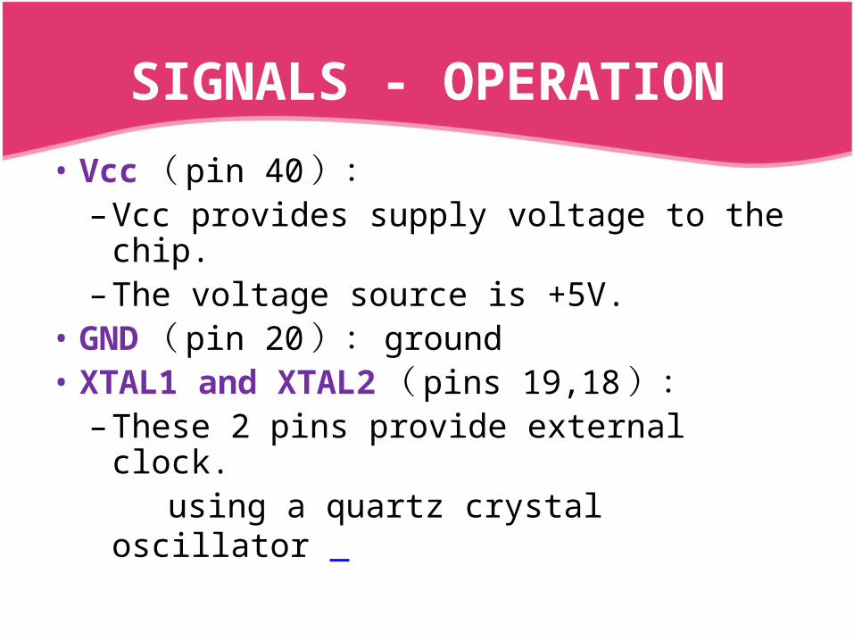
SIGNALS - OPERATION
• Vcc ( pin 40):– Vcc provides supply voltage to the chip. – The voltage source is +5V.
• GND ( pin 20): ground• XTAL1 and XTAL2 ( pins 19,18):
– These 2 pins provide external clock. using a quartz crystal oscillator
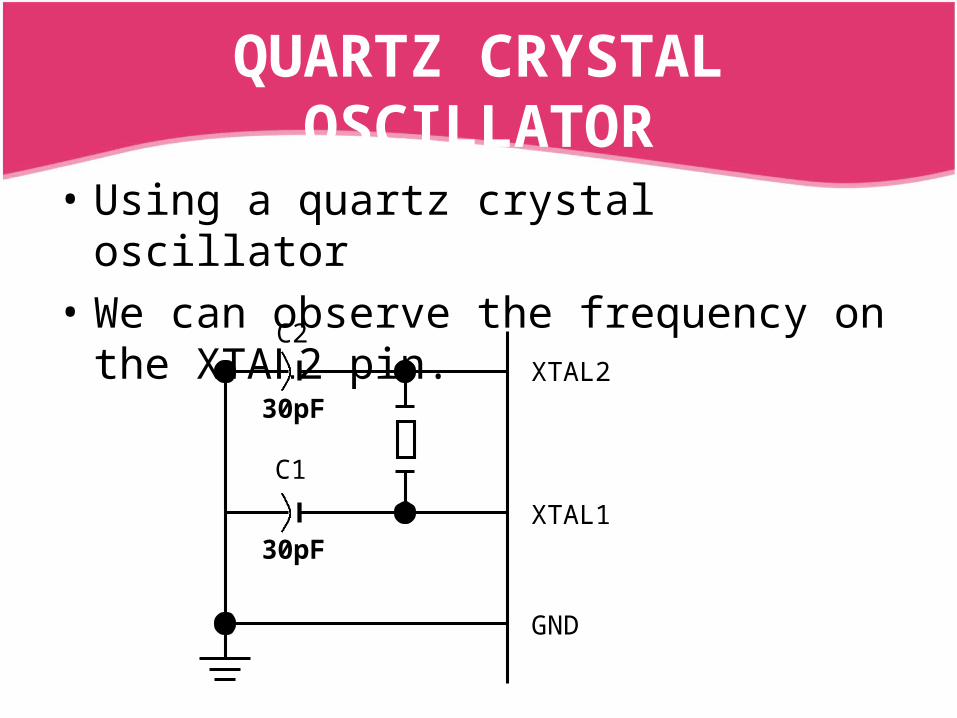
QUARTZ CRYSTAL OSCILLATOR
• Using a quartz crystal oscillator
• We can observe the frequency on the XTAL2 pin.
C2
30pF
C1
30pF
XTAL2
XTAL1
GND
RST - RESET
• RST ( pin 9): reset– input pin and active high
• The high pulse must be high at least 2 machine cycles.
– power-on reset.
• Upon applying a high pulse to RST, the microcontroller will reset and all values in registers will be lost.
• Reset values of some 8051 registers
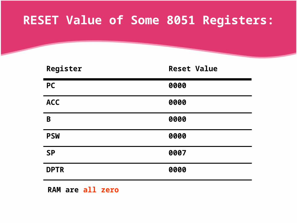
RESET Value of Some 8051 Registers:
0000DPTR
0007SP
0000PSW
0000B
0000ACC
0000PC
Reset ValueRegister
RAM are all zero

RESET CIRCUITARY
EA/VPPX1
X2RST
Vcc
10 uF
8.2 K
30 pF
9
31

17
BLOCK DESCRIPTION
• ACCUMULATOR ( ACC )• Operand register• Implicit or specified in the instruction• Has an address in on chip SFR bank
• B REGISTER• to store one of the operands for
multiplication and division• otherwise, scratch pad• considered as a SFR

18
PROGRAM STATUS WORD ( PSW )• Set of flags contain status information• One of the SFR
• STACK POINTER ( SP )• 8 bit wide register• Incremented before data is stored on to the
stack using PUSH or CALL instructions• Stack defined anywhere on the 128 byte
RAM• RESET initiated to 0007H• Not a top to down structure• Allotted an address in SFR

19
• DATA POINTER ( DPTR )• 16 bit register• contains DPH and DPL• Pointer to external RAM address• DPH and DPL allotted separate addresses in
SFR bank
• PORT 0 TO 3 LATCHES & DRIVERS• Each i/o port allotted a latch and a driver• Latches allotted address in SFR• User can communicate via these ports• P0, P1, P2,P3
20
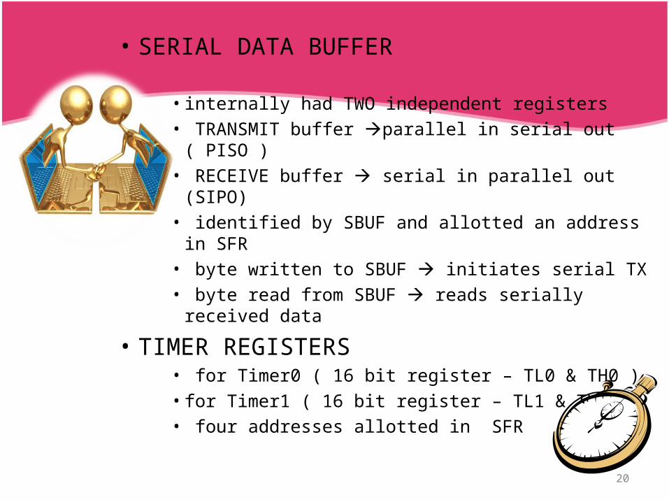
• SERIAL DATA BUFFER
• internally had TWO independent registers• TRANSMIT buffer parallel in serial out ( PISO )• RECEIVE buffer serial in parallel out (SIPO)• identified by SBUF and allotted an address in SFR• byte written to SBUF initiates serial TX• byte read from SBUF reads serially received
data
• TIMER REGISTERS• for Timer0 ( 16 bit register – TL0 & TH0 )• for Timer1 ( 16 bit register – TL1 & TH1 )• four addresses allotted in SFR

21
• OSCILLATOR• generates basic timing clock signal using crystal oscillator
• INSTRUCTION REGISTER• decodes the opcode and gives information to timing and
control unit• EPROM & PROGRAM ADDRESS REGISTER
• provide on chip EPROM and mechanism to address it• All versions don’t have EPROM
• RAM & RAM ADDRESS REGISTER• provide internal 128 bytes RAM and a mechanism to address internally

22
• ALU• Performs 8 bit arithmetic and logical
operations over the operands held by TEMP1 and TEMP 2
• User cannot access temporary registers
• SFR REGISTER BANK• set of special function registers• address range : 80 H to FF H

INSTRUCTIONS SET
• ARITHMETIC INSTRUCTIONS• LOGIC INSTRUCTIONS• BOOLEN INSTRUCTIONS• DATA TRANSFER INSTRUCTIONS• SINGLE BIT INSTRUCTIONS• JUMP,LOOP AND CALL INSTRUCTIONS

Arithmetic instructions
ADD,SUB,DIV,MUL,INC,DEC

add a, byte ; a a + byte
addc a, byte ; a a + byte + C
These instructions affect 3 bits in PSW:C = 1 if result of add is greater than FF
AC = 1 if there is a carry out of bit 3
OV = 1 if there is a carry out of bit 7,
but not from bit 6, or visa versa.
ADD & SUB
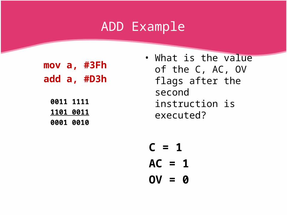
mov a, #3Fh
add a, #D3h
• What is the value of the C, AC, OV flags after the second instruction is executed?
0011 1111
1101 0011
0001 0010
C = 1
AC = 1
OV = 0
ADD Example
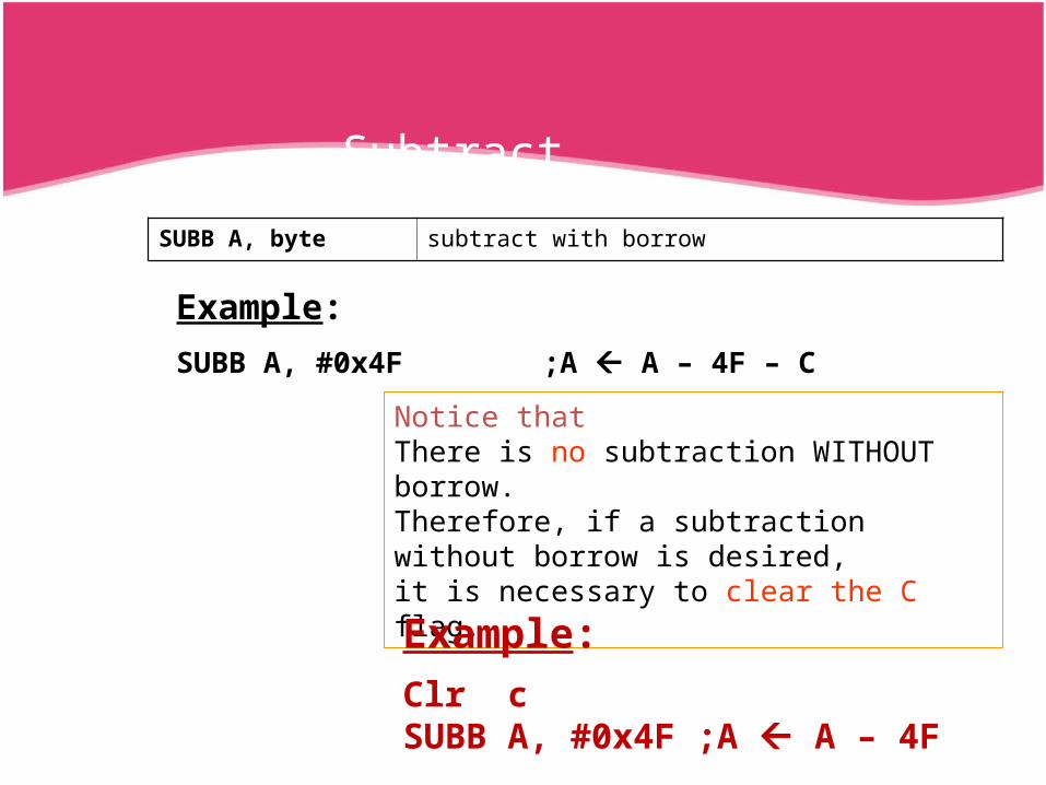
SUBB A, byte subtract with borrow
Example:
SUBB A, #0x4F ;A A – 4F – C
Notice that There is no subtraction WITHOUT borrow. Therefore, if a subtraction without borrow is desired, it is necessary to clear the C flag.
Example:
Clr cSUBB A, #0x4F ;A A – 4F
Subtract

• The increment and decrement instructions do NOT affect the C flag.
• Notice we can only INCREMENT the data pointer, not decrement.
INC A increment A
INC byte increment byte in memory
INC DPTR increment data pointer
DEC A decrement accumulator
DEC byte decrement byte
Increment & Decrement

• Assume 16-bit word in R3:R2mov a, r2
add a, #1 ; use add rather than increment to affect C
mov r2, a mov a, r3 addc a, #0 ; add C to most significant bytemov r3, a
SIGNIFICANCE OF carry flag
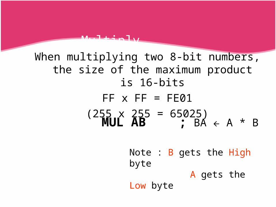
When multiplying two 8-bit numbers, the size of the maximum product is 16-bits
FF x FF = FE01(255 x 255 = 65025)
MUL AB ; BA A * B
Note : B gets the High byte A gets the Low byte
Multiply

• Integer Division
DIV AB ; divide A by B
A Quotient(A/B) B Remainder(A/B)
OV - used to indicate a divide by zero condition.
C – set to zero
Division
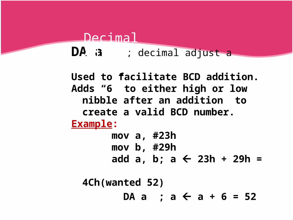
DA a ; decimal adjust a
Used to facilitate BCD addition. Adds “6” to either high or low nibble after an
addition to create a valid BCD number.Example:
mov a, #23hmov b, #29hadd a, b; a 23h + 29h =
4Ch(wanted 52)
DA a ; a a + 6 = 52
Decimal Adjust
BOOLEAN INSTRUCTIONS
CLR,CPL,SETB,AND,OR

BOOLEAN INSTRUCTIONS• This group of instructions is associated with the single-bit
operations of the 8051.• This group allows manipulating the individual bits of bit
addressable registers and memory locations as well as the CY flag.– The P, OV, and AC flags cannot be directly altered.
• This group includes:– Set, clear, and, or complement, move.– Conditional jumps.

CLR <bit>
CLR C• CLR instruction can operate
on the carry flag• CLR C• The CARRY flag is set to 0
CLR bit• CLR instruction can operate
on any directly addressable bitCLR P2.7• If Port 2 has been previously
written with DCH (11011100),• then the operation leaves the
port set to 5CH (01011100)

SETB <bit>
SETB C• SETB instruction operates
on the carry flag and sets the specified bit to 1
• SETB C• sets the carry flag to 1
SETB bit• SETB instruction operates
on any directly-addressable bit and
sets the specified bit to 1• SETB P2.0• Port 2 has the value of 24H
(00100100), the Port 2 value changes to 25H (00100101)

CPL <bit>
CPL C• This operation
complements the carry flag• CPL C
CPL bit• CPL instruction complements
any directly addressable Bit• CPL P2.2• If Port 2 has the value of 53H
(01010011) then after the execution the port set to 55H (01010101)
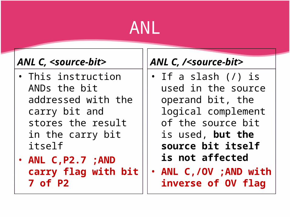
ANL
ANL C, <source-bit>• This instruction ANDs the
bit addressed with the carry bit and stores the result in the carry bit itself
• ANL C,P2.7 ;AND carry flag with bit 7 of P2
ANL C, /<source-bit>• If a slash (/) is used in the
source operand bit, the logical complement of the source bit is used, but the source bit itself is not affected
• ANL C,/OV ;AND with inverse of OV flag
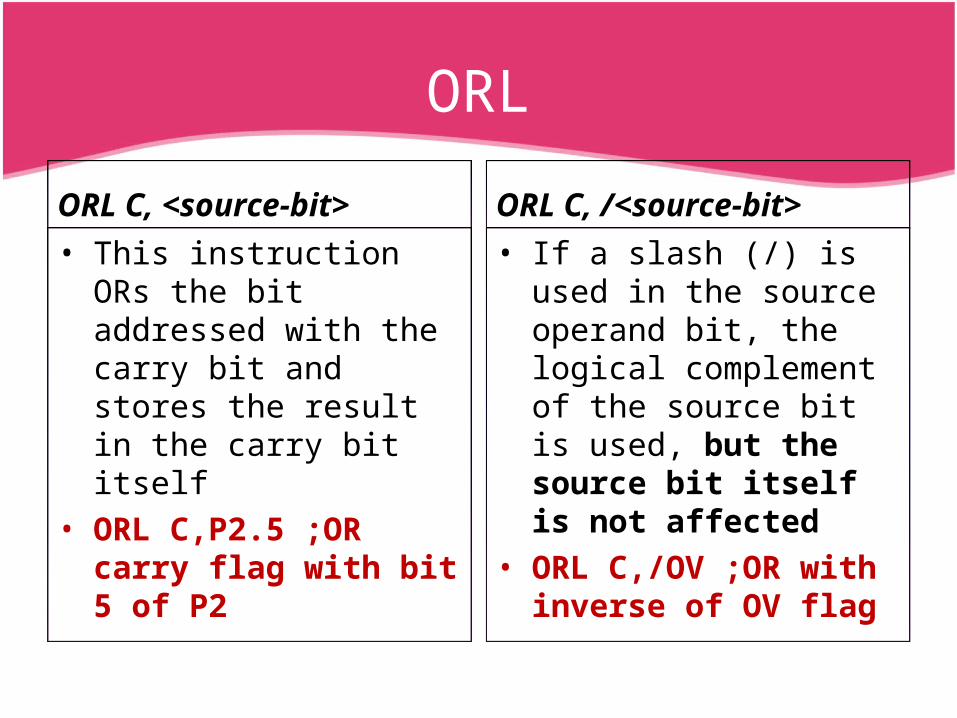
ORL
ORL C, <source-bit>• This instruction ORs the bit
addressed with the carry bit and stores the result in the carry bit itself
• ORL C,P2.5 ;OR carry flag with bit 5 of P2
ORL C, /<source-bit>• If a slash (/) is used in the
source operand bit, the logical complement of the source bit is used, but the source bit itself is not affected
• ORL C,/OV ;OR with inverse of OV flag
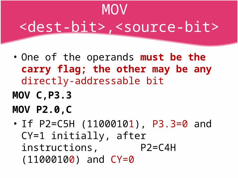
MOV <dest-bit>,<source-bit>
• One of the operands must be the carry flag; the other may be any directly-addressable bit
MOV C,P3.3MOV P2.0,C• If P2=C5H (11000101), P3.3=0 and CY=1 initially,
after instructions, P2=C4H (11000100) and CY=0
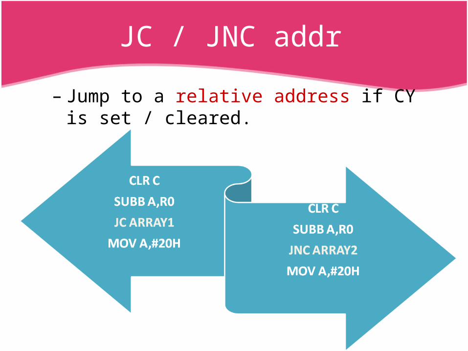
JC / JNC addr
– Jump to a relative address if CY is set / cleared.
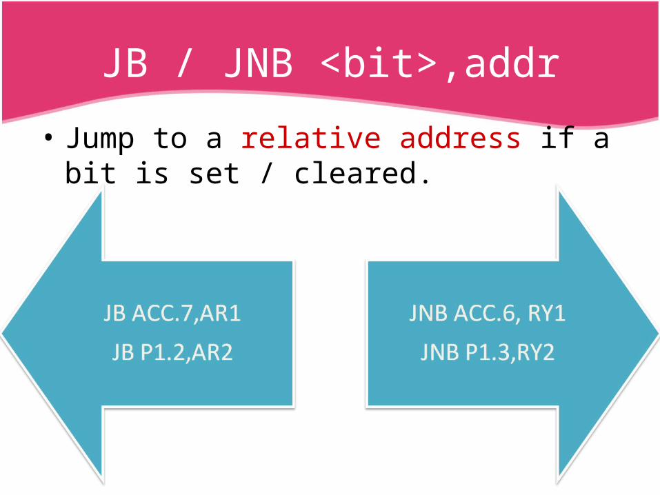
JB / JNB <bit>,addr
• Jump to a relative address if a bit is set / cleared.
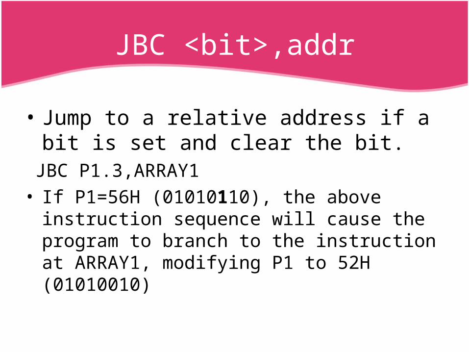
JBC <bit>,addr
• Jump to a relative address if a bit is set and clear the bit.
JBC P1.3,ARRAY1• If P1=56H (01010110), the above instruction sequence
will cause the program to branch to the instruction at ARRAY1, modifying P1 to 52H (01010010)

BRANCH INSTRUCTIONS
CALL, JMP, RET
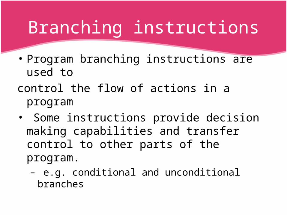
Branching instructions
• Program branching instructions are used tocontrol the flow of actions in a program• Some instructions provide decision making
capabilities and transfer control to other parts of the program.– e.g. conditional and unconditional branches
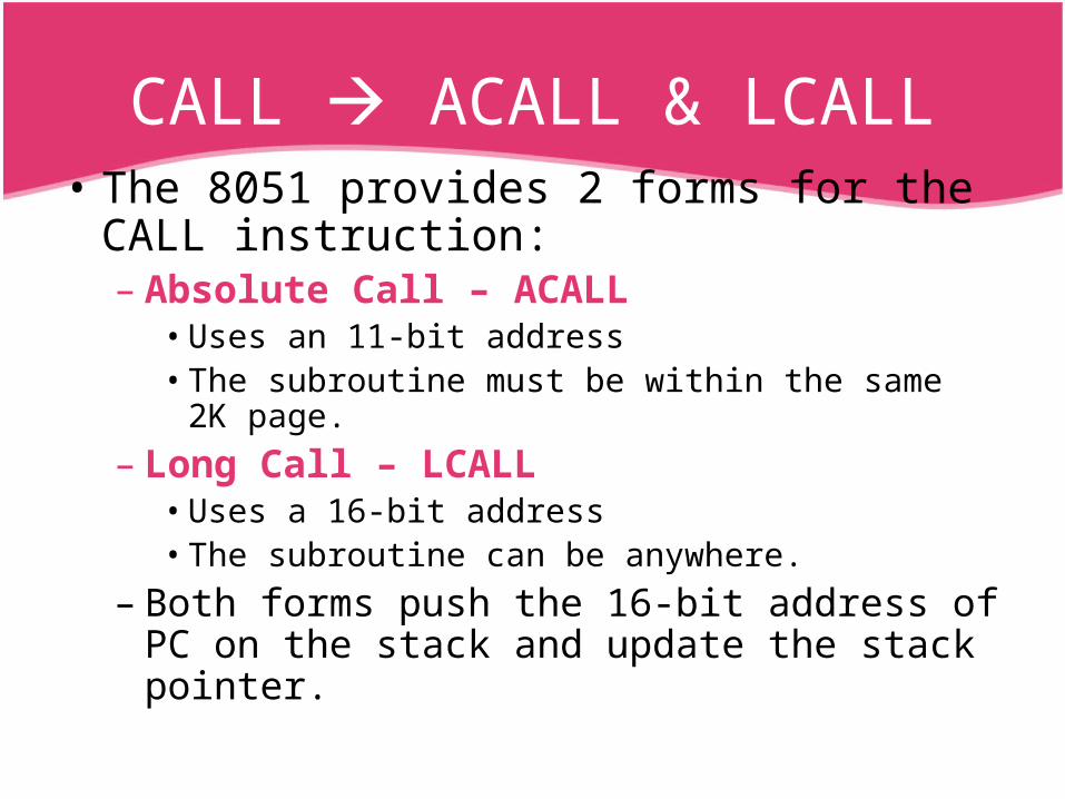
CALL ACALL & LCALL• The 8051 provides 2 forms for the CALL
instruction:– Absolute Call – ACALL
• Uses an 11-bit address• The subroutine must be within the same 2K page.
– Long Call – LCALL• Uses a 16-bit address• The subroutine can be anywhere.
– Both forms push the 16-bit address of PC on the stack and update the stack pointer.

Absolute Call – ACALL addr11
• This instruction unconditionally calls a subroutine indicated by the address
• 2 byte instruction: The upper 3-bits of the address combine with the 5-bit opcode to form the 1st byte and the lower 8-bits of the address form the 2nd byte
Eg. ACALL LOC_SUB• If SP=07H initially • label “LOC_SUB” is at memory 0567H,• then executing instruction at 0230H (PC),
– SP=09H, internal RAM locations 08H and 09H will contain 32Hand 02H respectively and PC=0567H
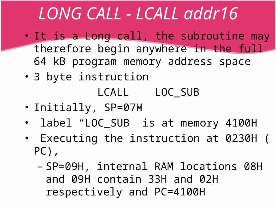
LONG CALL - LCALL addr16• It is a Long call, the subroutine may therefore begin
anywhere in the full 64 kB program memory address space
• 3 byte instructionLCALL LOC_SUB
• Initially, SP=07H • label “LOC_SUB” is at memory 4100H• Executing the instruction at 0230H ( PC),
– SP=09H, internal RAM locations 08H and 09H contain 33H and 02H respectively and PC=4100H

RETURN RET & RETI• The 8051 provides 2 forms for the return
instruction:– Return from subroutine – RET
• Pop the return address from the stack and continue execution there.
– Return from ISR – RETI• Pop the return address from the stack.• Restore the interrupt logic to accept additional
interrupts at the same priority level as the one just processed.
• Continue execution at the address retrieved from the stack.
• The PSW is not automatically restored.
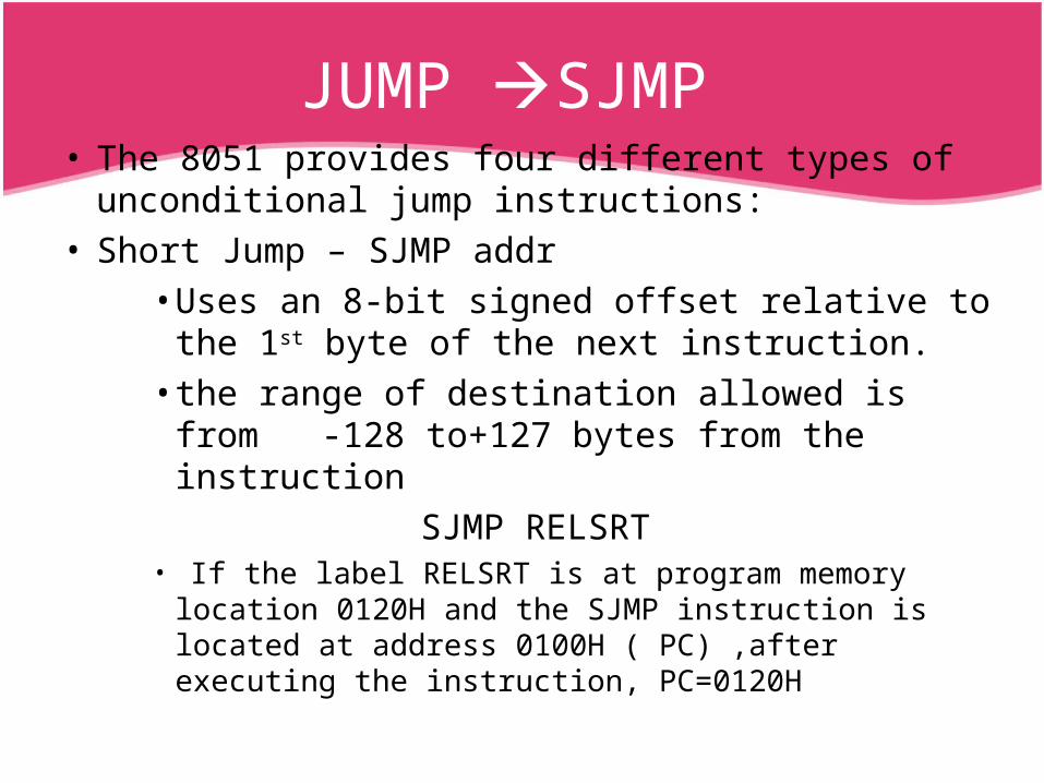
JUMP SJMP • The 8051 provides four different types of
unconditional jump instructions:• Short Jump – SJMP addr
• Uses an 8-bit signed offset relative to the 1st byte of the next instruction.
• the range of destination allowed is from -128 to+127 bytes from the instruction
SJMP RELSRT• If the label RELSRT is at program memory location 0120H
and the SJMP instruction is located at address 0100H ( PC) ,after executing the instruction, PC=0120H

JUMP LJMP• Long Jump – LJMP
• Uses a 16-bit address.• 3 byte instruction capable of referencing any
location in the entire 64K of program memory.LJMP FAR_ADR
• If the label FAR_ADR is at program memory location 3456H– the LJMP instruction at location 0120H (PC)– After instruction, it loads the PC with 3456H
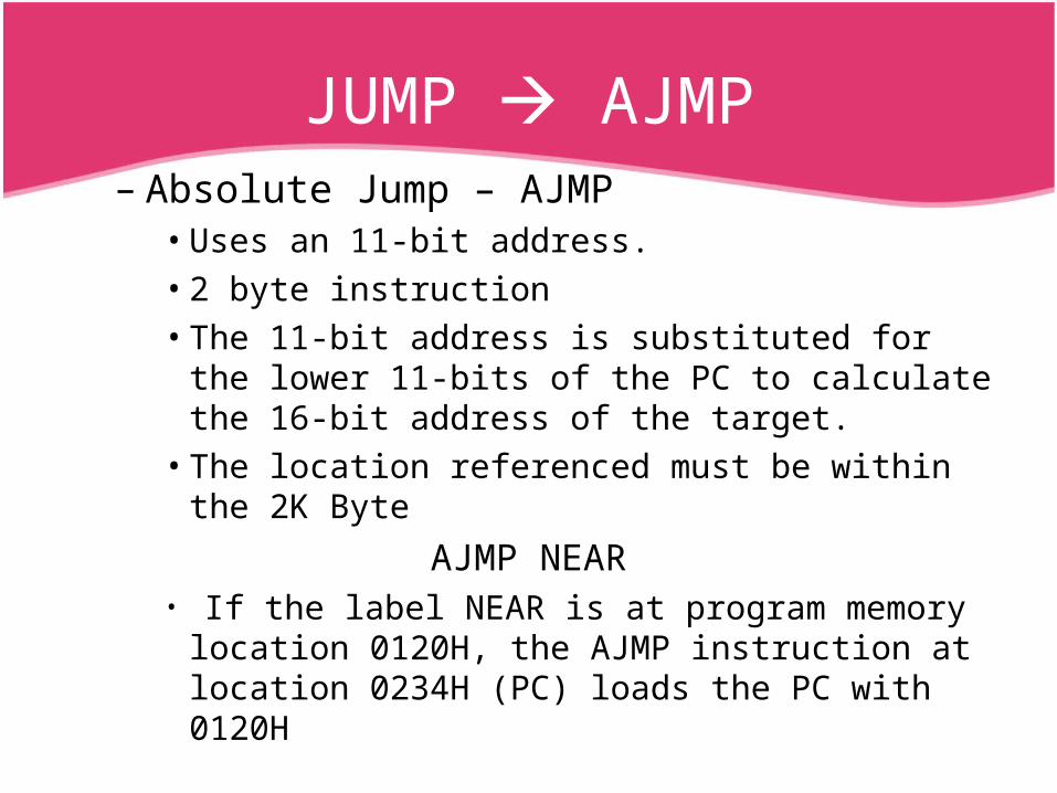
JUMP AJMP– Absolute Jump – AJMP
• Uses an 11-bit address.• 2 byte instruction• The 11-bit address is substituted for the lower 11-bits
of the PC to calculate the 16-bit address of the target.• The location referenced must be within the 2K Byte
AJMP NEAR• If the label NEAR is at program memory location
0120H, the AJMP instruction at location 0234H (PC) loads the PC with 0120H

Indirect Jump
• This instruction adds the 8-bit unsigned value of the ACC to the 16-bit data pointer and the resulting sum is returned to the PC
• Neither ACC nor DPTR is altered• No flags are affected
MOV DPTR, #LOOK_TBLJMP @A + DPTR
LOOK_TBL: AJMP LOC0AJMP LOC1AJMP LOC2
• If the ACC=02H, execution jumps to LOC2• AJMP is a two byte instruction
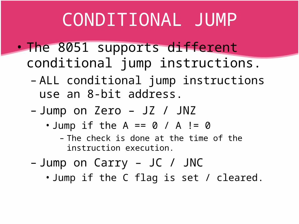
CONDITIONAL JUMP• The 8051 supports different conditional jump
instructions.– ALL conditional jump instructions use an 8-bit
address.– Jump on Zero – JZ / JNZ
• Jump if the A == 0 / A != 0– The check is done at the time of the instruction execution.
– Jump on Carry – JC / JNC• Jump if the C flag is set / cleared.
CONDITIONAL JUMP
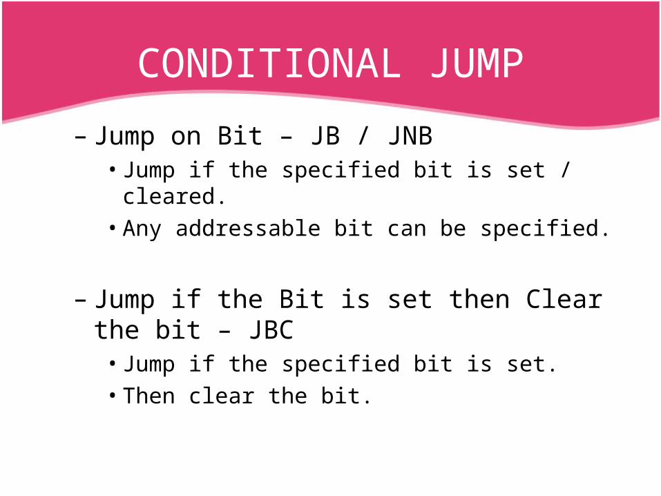
– Jump on Bit – JB / JNB• Jump if the specified bit is set / cleared.• Any addressable bit can be specified.
– Jump if the Bit is set then Clear the bit – JBC• Jump if the specified bit is set.• Then clear the bit.

Compare and Jump if Not Equal – CJNE
– Compare the magnitude of the two operands and jump if they are not equal.
• The values are considered to be unsigned.• The Carry flag is set / cleared appropriately.• CJNE A, direct, rel• CJNE A, #data, rel• CJNE Rn, #data, rel• CJNE @Ri, #data, rel

Decrement and Jump if Not Zero – DJNZ
– Decrement the first operand by 1 and jump to the location identified by the second operand if the resulting value is not zero.
DJNZ 20H,LOC1DJNZ 30H,LOC2DJNZ 40H,LOC3
• If internal RAM locations 20H, 30H and 40H contain the values 01H, 5FH and 16H respectively,
• the above instruction sequence will cause a jump to the instruction at LOC2, with the values 00H, 5EH, and 15H in the 3 RAM locations

NOP• This is the no operation instruction• The instruction takes one machine cycle operation
time• Hence it is useful to time the ON/OFF bit of an output
portCLR P1.2
NOPNOPNOPNOP
SETB P1.2

59
LOGICAL INSTRUCTIONS
AND,OR,NOT,XOR,ROTATE,SWAP
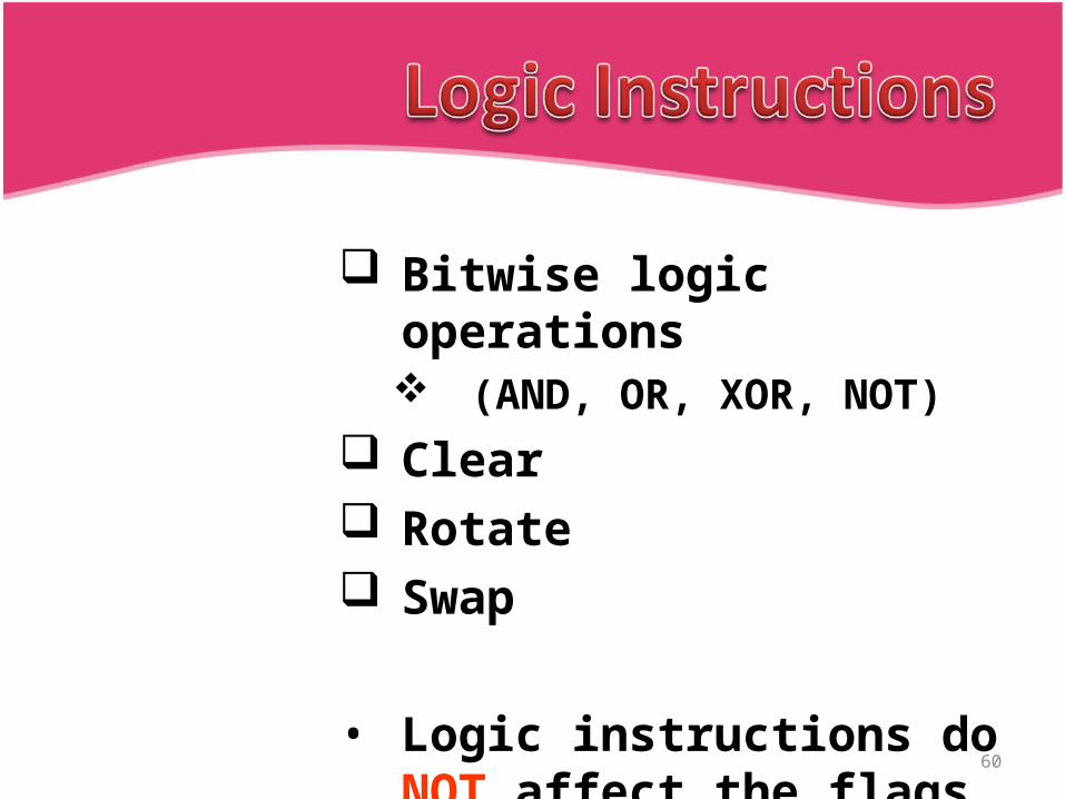
60
Bitwise logic operations (AND, OR, XOR, NOT)
Clear Rotate Swap
• Logic instructions do NOT affect the flags in PSW

61
Bitwise Logic
ANL AND
ORL OR
XRL XOR
CPL Complement
Examples:0000111110101100ANL
0000111110101100ORL
0000111110101100XRL
10101100CPL
00001100
10101111
10100011
01010011

62
anl PSW, #0xE7;PSW AND 11100111orl PSW, #0x18;PSW OR 00011000xrl P1, #0x40;P1 XRL 01000000
63
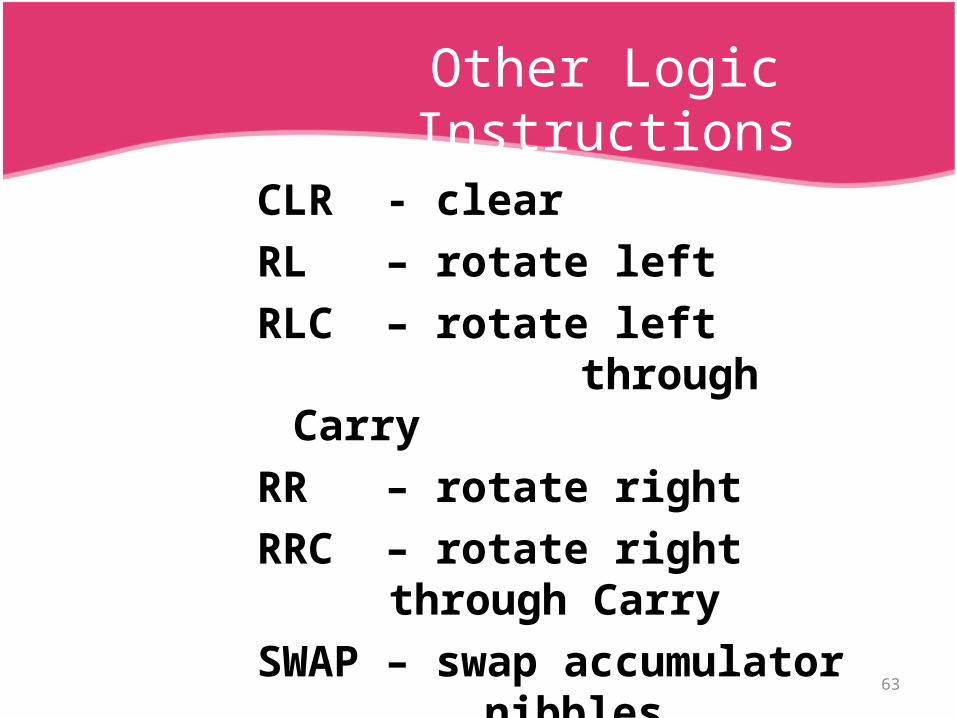
Other Logic Instructions
CLR - clear
RL – rotate left
RLC – rotate left through Carry
RR – rotate right
RRC – rotate right through Carry
SWAP – swap accumulator nibbles
64
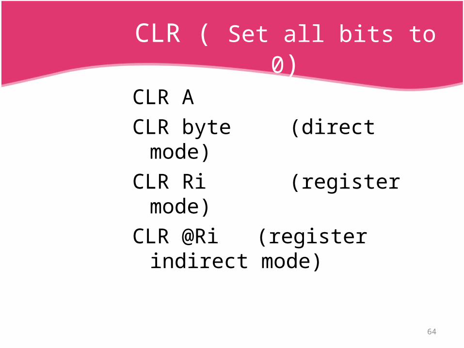
CLR ( Set all bits to 0)
CLR ACLR byte (direct mode)CLR Ri (register mode)CLR @Ri (register indirect mode)
65
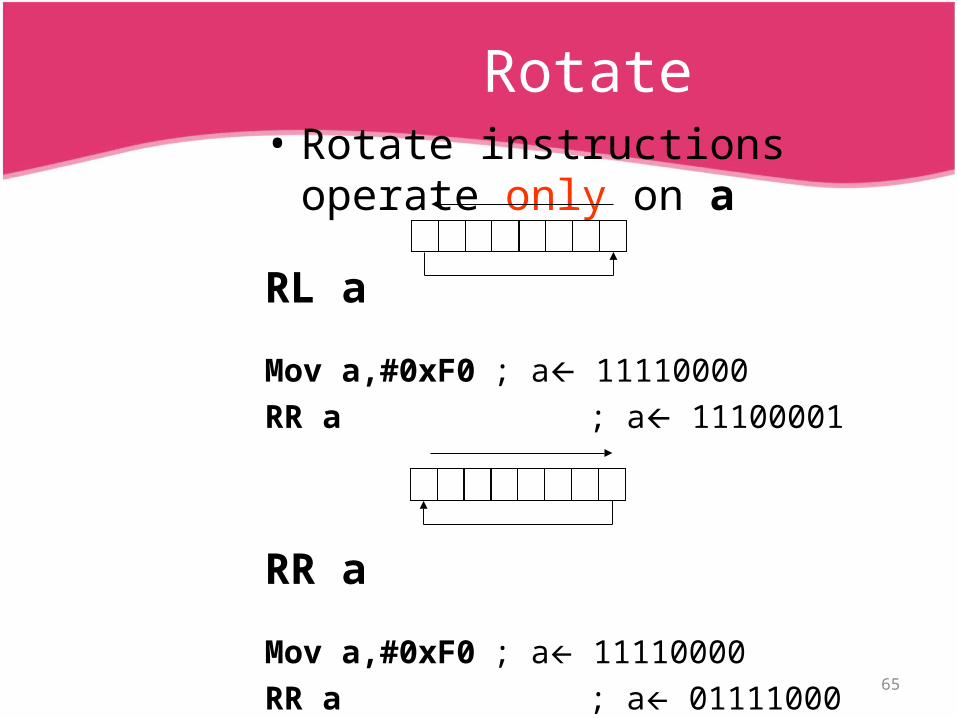
Rotate• Rotate instructions operate only on a
RL a
Mov a,#0xF0 ; a 11110000
RR a ; a 11100001
RR a
Mov a,#0xF0 ; a 11110000
RR a ; a 01111000

66
Rotate through Carry
RRC a
mov a, #0A9h ; a A9add a, #14h ; a BD (10111101),
C0
rrc a ; a 01011110, C1
RLC a
mov a, #3ch ; a 3ch(00111100)setb c ; c 1
rlc a ; a 01111001, C1
C
C
67
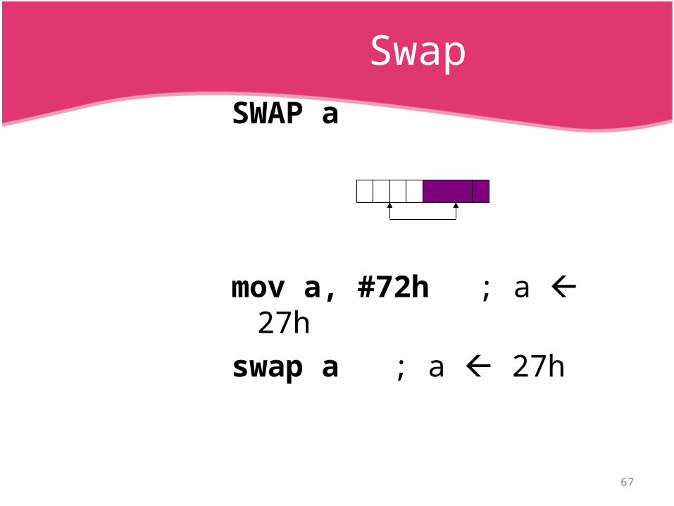
SwapSWAP a
mov a, #72h ; a 27h
swap a ; a 27h

68
Rotate and Multiplication/Division
• Note that a shift left is the same as multiplying by 2, shift right is divide by 2mov a, #3; A 00000011 (3)
clr C ; C 0
rlc a ; A 00000110(6)
rlc a ; A 0000110(12)
rrc a ; A 00000110(6)

69

Computers transfer data in two ways:
• Parallel Often 8 or more lines (wire conductors) are used to transfer data to
a device that is only a few feet away.
• Serial To transfer to a device located many meters away, the serial
method is used. The data is sent one bit at a time.
70

71

Serial Communication b/w micro controller & LCD.
72
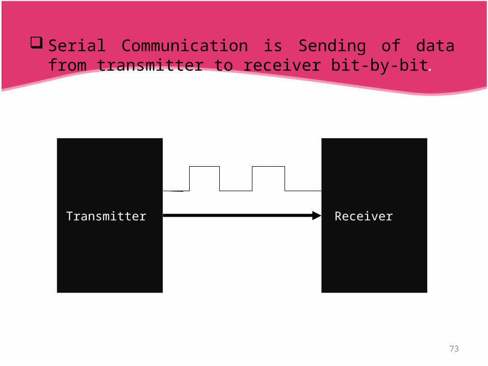
Serial Communication is Sending of data from transmitter to receiver bit-by-bit.
73
Transmitter Receiver

• For long distances.• Low Cost.
74
• The speed of serial Communication is very slow than parallel communication.
•
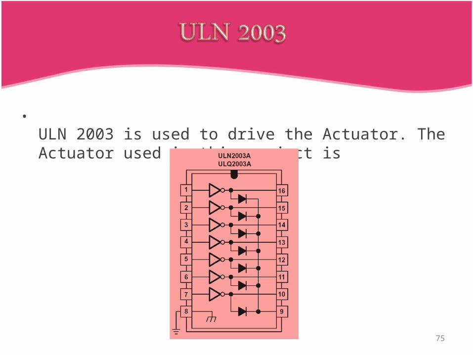
ULN 2003 is used to drive the Actuator. The Actuator used in this project is Stepper Motor.
• Pin Diagram of ULN 2003
75

76
• To control stepper motor , DC motor. Servomotor.
• To operate Relays.
77

How to use KEIL c• STEPS TO ACCESS µVISION:
• Double Click on the icon present on the desktop.• The following window will be popped-up
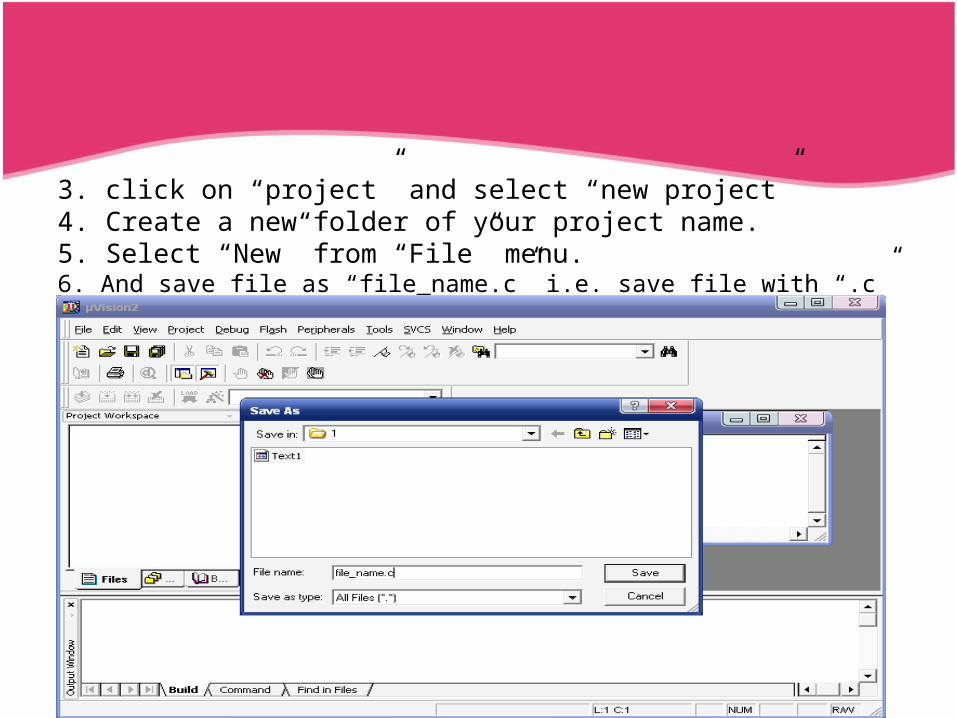
3. click on “project” and select “new project”4. Create a new folder of your project name.5. Select “New” from “File” menu.6. And save file as “file_name.c” i.e. save file with “.c” extension.

• 7. Select device for target as shown in figure below.
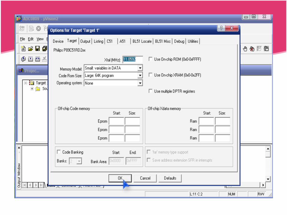
• 8. Configure Device and select clock 11.0592MHZ.
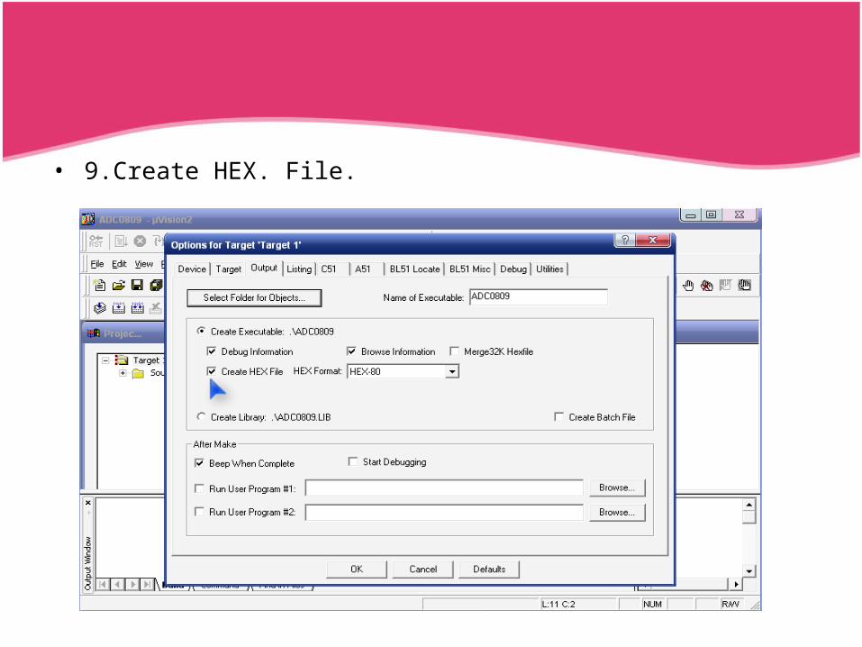
• 9.Create HEX. File.

• 10. Press right click and select “INSERT #include<REGF51.H>”.

• 11. Type the application code and after compiling, saving the code burn it into controller using
• “Flash Mazic”.