methods of designing analog-to-digital...
TRANSCRIPT
1
IHP Im Technologiepark 25 15236 Frankfurt (Oder) Germany www.ihp-microelectronics.com © 2011 - All rights reservedElena Shvaichenko
METHODS OF DESIGNING ANALOG-TO-DIGITAL
CONVERTERSMaster’s Thesis Presentation
Author: Olena Shvaichenko
2
IHP Im Technologiepark 25 15236 Frankfurt (Oder) Germany www.ihp-microelectronics.com © 2011 - All rights reservedElena Shvaichenko
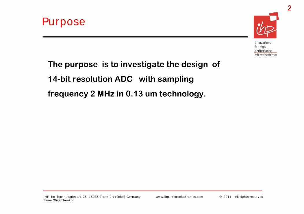
The purpose is to investigate the design of
14-bit resolution ADC with sampling
frequency 2 MHz in 0.13 um technology.
Purpose
3
IHP Im Technologiepark 25 15236 Frankfurt (Oder) Germany www.ihp-microelectronics.com © 2011 - All rights reservedElena Shvaichenko
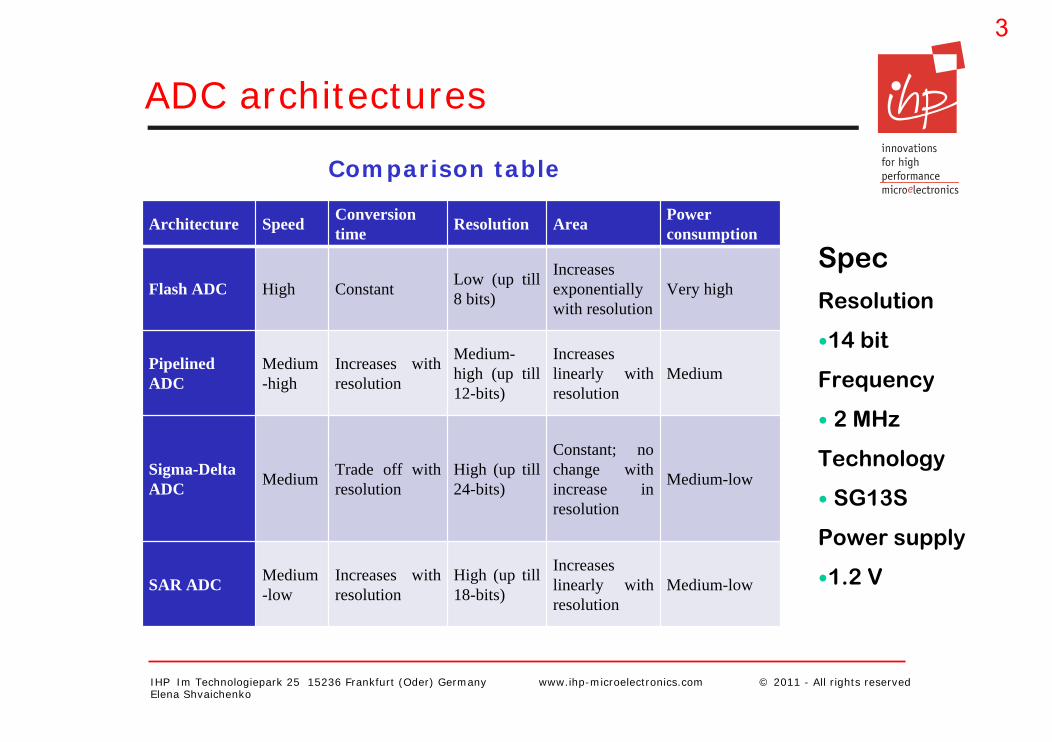
Architecture Speed Conversiontime Resolution Area Power
consumption
Flash ADC High Constant Low (up till8 bits)
Increasesexponentiallywith resolution
Very high
PipelinedADC
Medium-high
Increases withresolution
Medium-high (up till 12-bits)
Increaseslinearly withresolution
Medium
Sigma-DeltaADC Medium Trade off with
resolutionHigh (up till24-bits)
Constant; no change with increase in resolution
Medium-low
SAR ADC Medium-low
Increases withresolution
High (up till18-bits)
Increaseslinearly withresolution
Medium-low
SpecResolution
14 bit
Frequency
2 MHz
Technology
SG13S
Power supply
1.2 V
ADC architectures
Comparison table
4
IHP Im Technologiepark 25 15236 Frankfurt (Oder) Germany www.ihp-microelectronics.com © 2011 - All rights reservedElena Shvaichenko
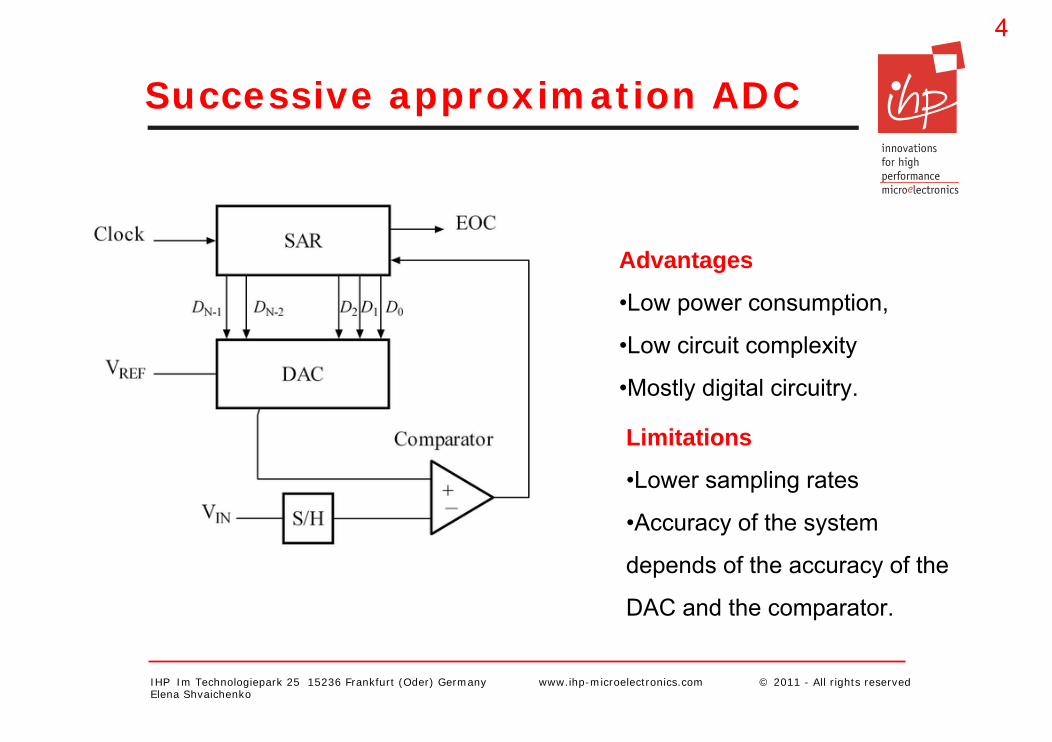
Advantages
•Low power consumption,
•Low circuit complexity
•Mostly digital circuitry.
Limitations
•Lower sampling rates
•Accuracy of the system
depends of the accuracy of the
DAC and the comparator.
Successive approximation ADC
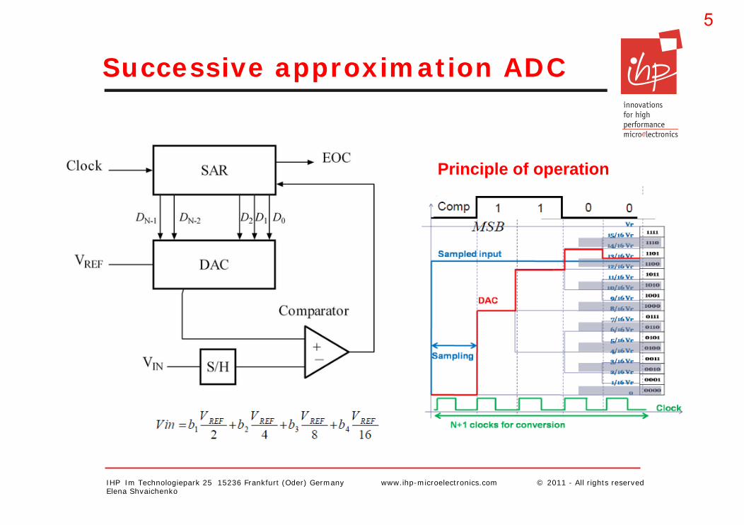
5
IHP Im Technologiepark 25 15236 Frankfurt (Oder) Germany www.ihp-microelectronics.com © 2011 - All rights reservedElena Shvaichenko
Principle of operation
Successive approximation ADC
6
IHP Im Technologiepark 25 15236 Frankfurt (Oder) Germany www.ihp-microelectronics.com © 2011 - All rights reservedElena Shvaichenko
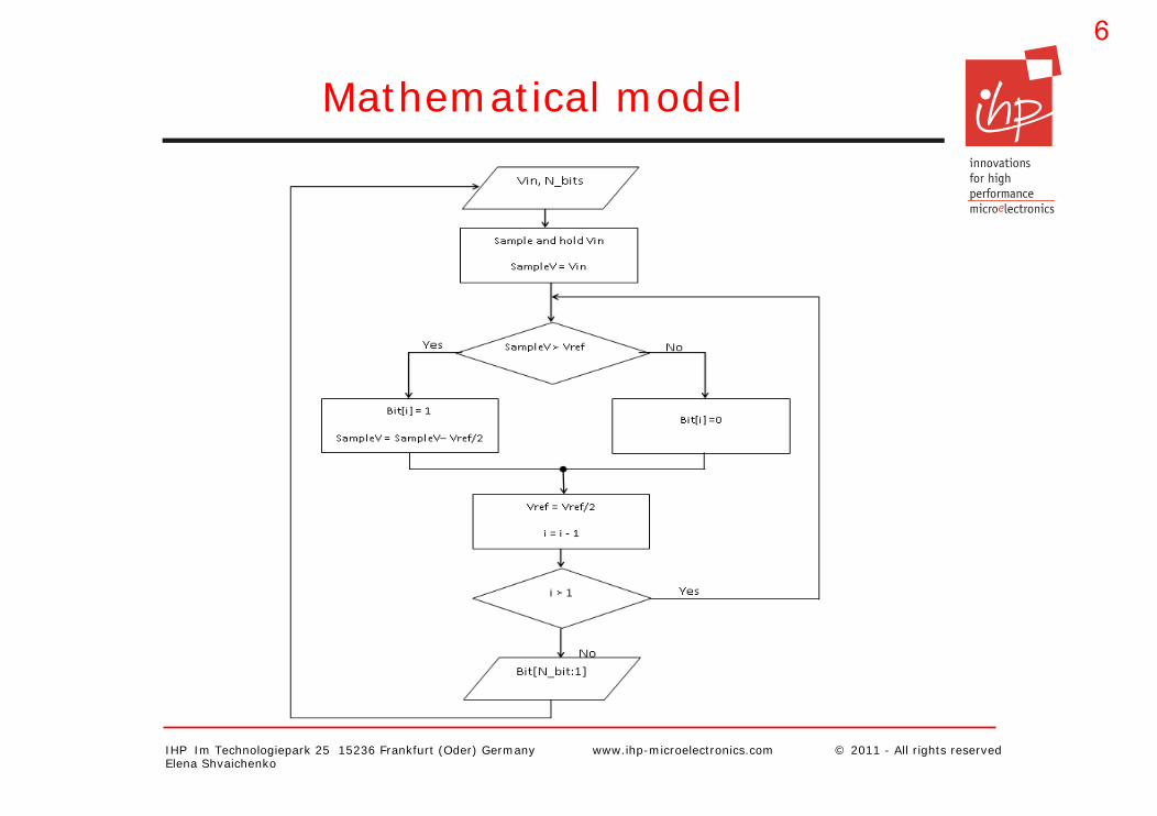
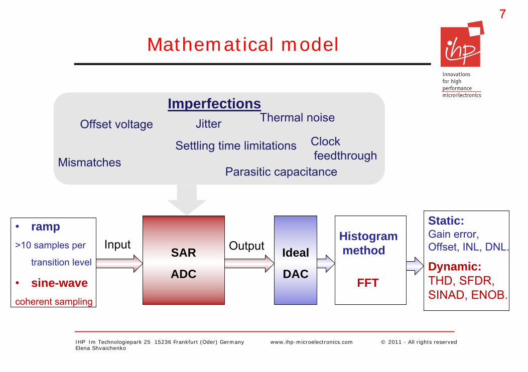
Mathematical model
7
IHP Im Technologiepark 25 15236 Frankfurt (Oder) Germany www.ihp-microelectronics.com © 2011 - All rights reservedElena Shvaichenko
Mathematical model
SAR
ADC
Input Output Ideal
DAC
Histogrammethod
FFT
• ramp >10 samples per
transition level
• sine-wavecoherent sampling
Static:Gain error, Offset, INL, DNL.
Dynamic:THD, SFDR, SINAD, ENOB.
Mismatches
Offset voltage
Settling time limitations
Imperfections
Parasitic capacitance
Thermal noise
Clockfeedthrough
Jitter
8
IHP Im Technologiepark 25 15236 Frankfurt (Oder) Germany www.ihp-microelectronics.com © 2011 - All rights reservedElena Shvaichenko
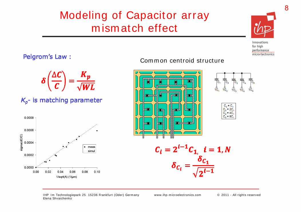
Modeling of Capacitor array mismatch effect
Common centroid structure
9
IHP Im Technologiepark 25 15236 Frankfurt (Oder) Germany www.ihp-microelectronics.com © 2011 - All rights reservedElena Shvaichenko
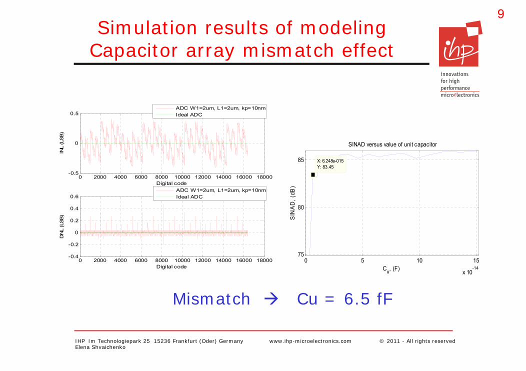
Simulation results of modeling Capacitor array mismatch effect
0 2000 4000 6000 8000 10000 12000 14000 16000 18000-0.5
0
0.5
Digital code
INL
(LS
B)
0 2000 4000 6000 8000 10000 12000 14000 16000 18000-0.4
-0.2
0
0.2
0.4
0.6
Digital code
DN
L (L
SB
)
ADC W1=2um, L1=2um, kp=10nmIdeal ADC
ADC W1=2um, L1=2um, kp=10nmIdeal ADC
0 5 10 15
x 10-14
75
80
85 X: 6.248e-015Y: 83.45
SINAD versus value of unit capacitor
Cu, (F)
SIN
AD
, (dB
)Mismatch Cu = 6.5 fF
10
IHP Im Technologiepark 25 15236 Frankfurt (Oder) Germany www.ihp-microelectronics.com © 2011 - All rights reservedElena Shvaichenko
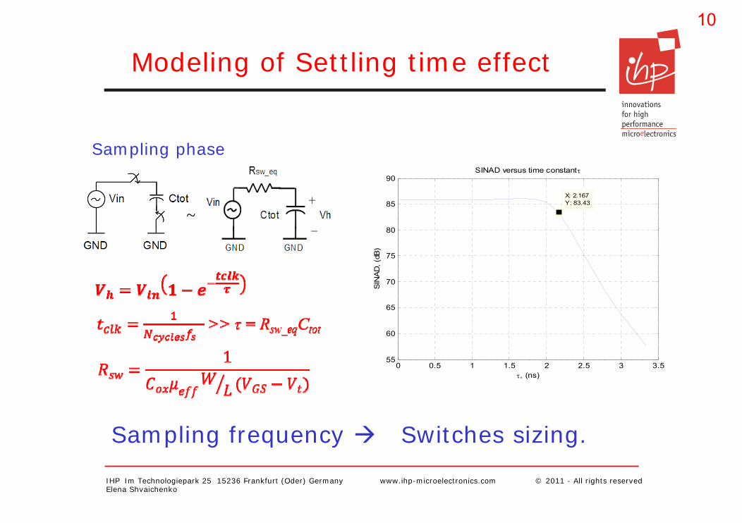
Modeling of Settling time effect
Sampling frequency Switches sizing.
~
Sampling phase
0 0.5 1 1.5 2 2.5 3 3.555
60
65
70
75
80
85
90
X: 2.167Y: 83.43
SINAD versus time constant τ
τ, (ns)S
INA
D, (
dB)
11
IHP Im Technologiepark 25 15236 Frankfurt (Oder) Germany www.ihp-microelectronics.com © 2011 - All rights reservedElena Shvaichenko
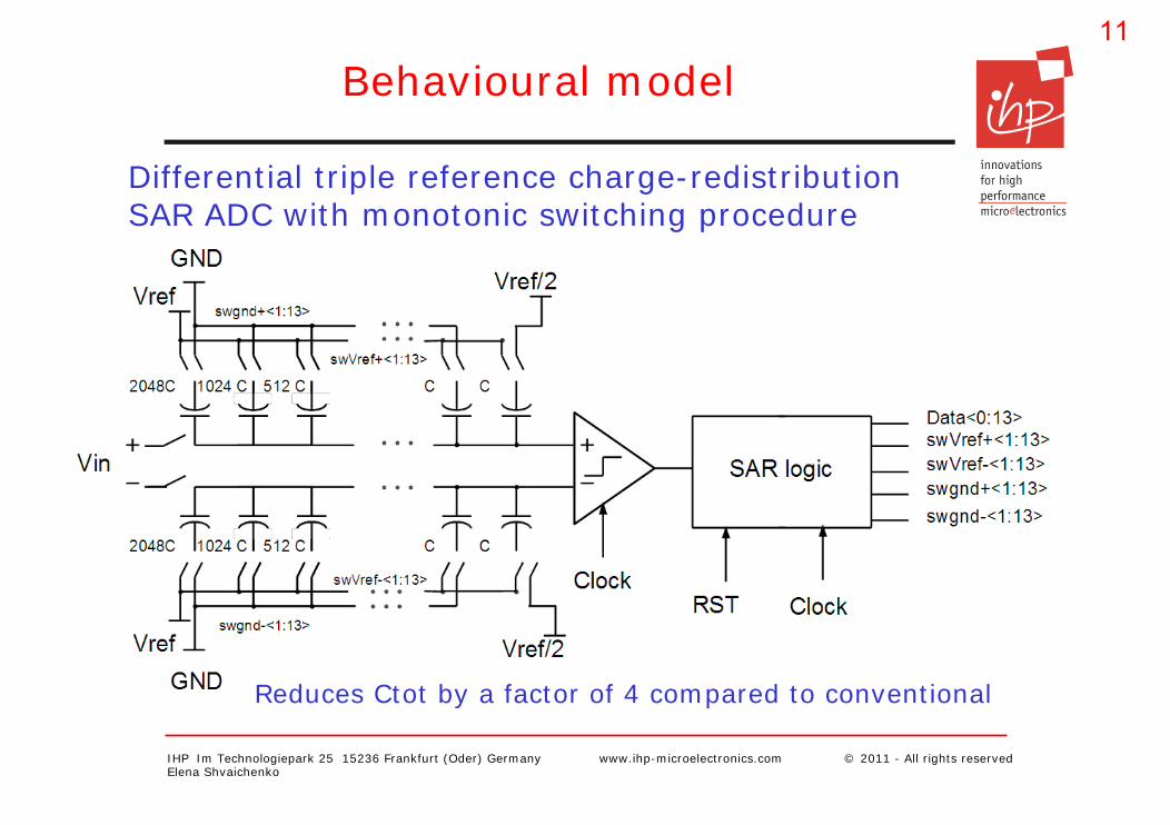
Behavioural model
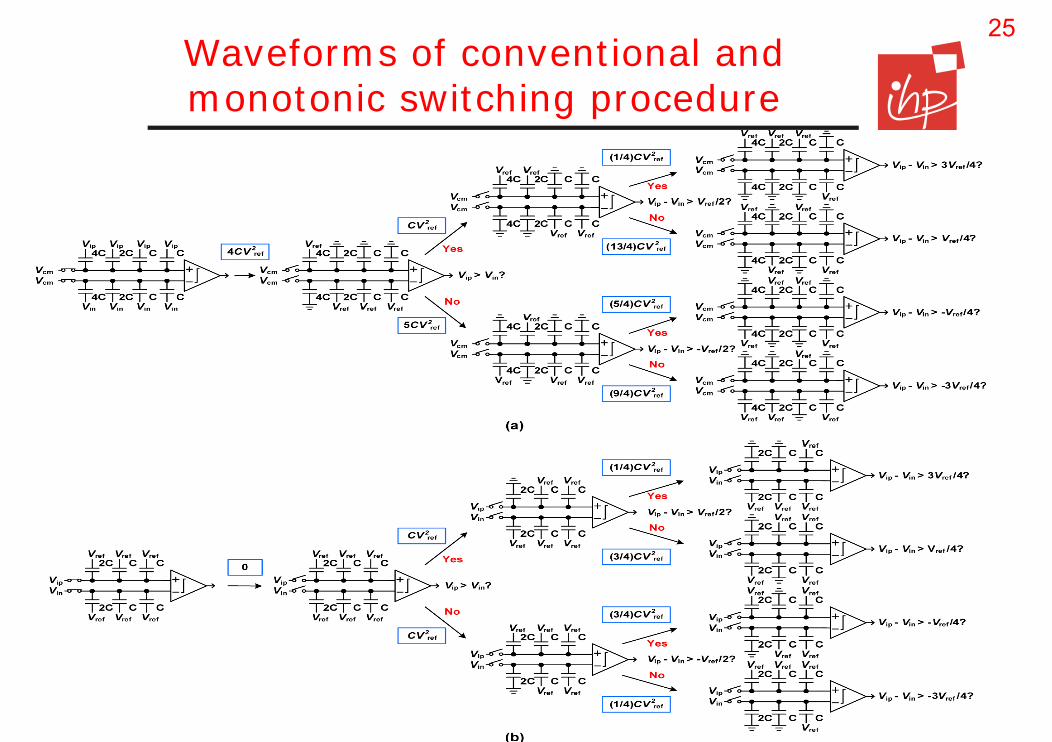
Differential triple reference charge-redistribution SAR ADC with monotonic switching procedure
Reduces Ctot by a factor of 4 compared to conventional
12
IHP Im Technologiepark 25 15236 Frankfurt (Oder) Germany www.ihp-microelectronics.com © 2011 - All rights reservedElena Shvaichenko
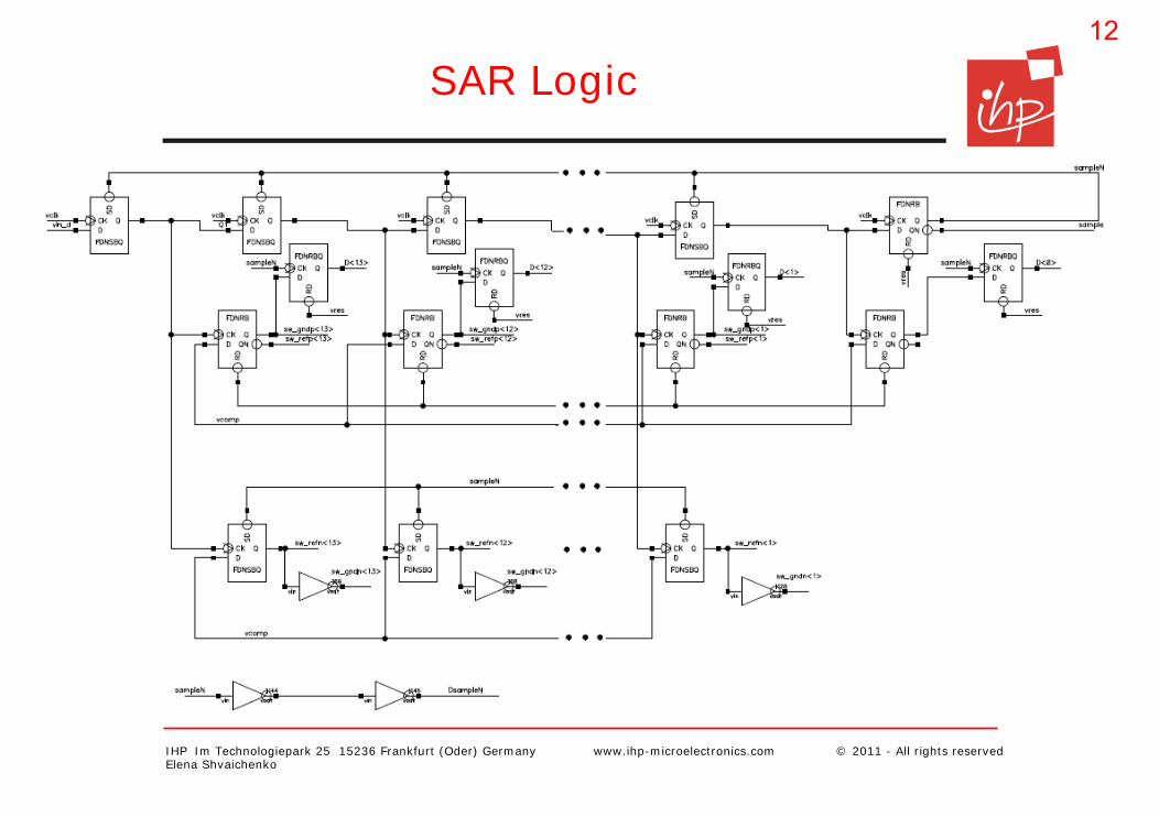
SAR Logic
13
IHP Im Technologiepark 25 15236 Frankfurt (Oder) Germany www.ihp-microelectronics.com © 2011 - All rights reservedElena Shvaichenko
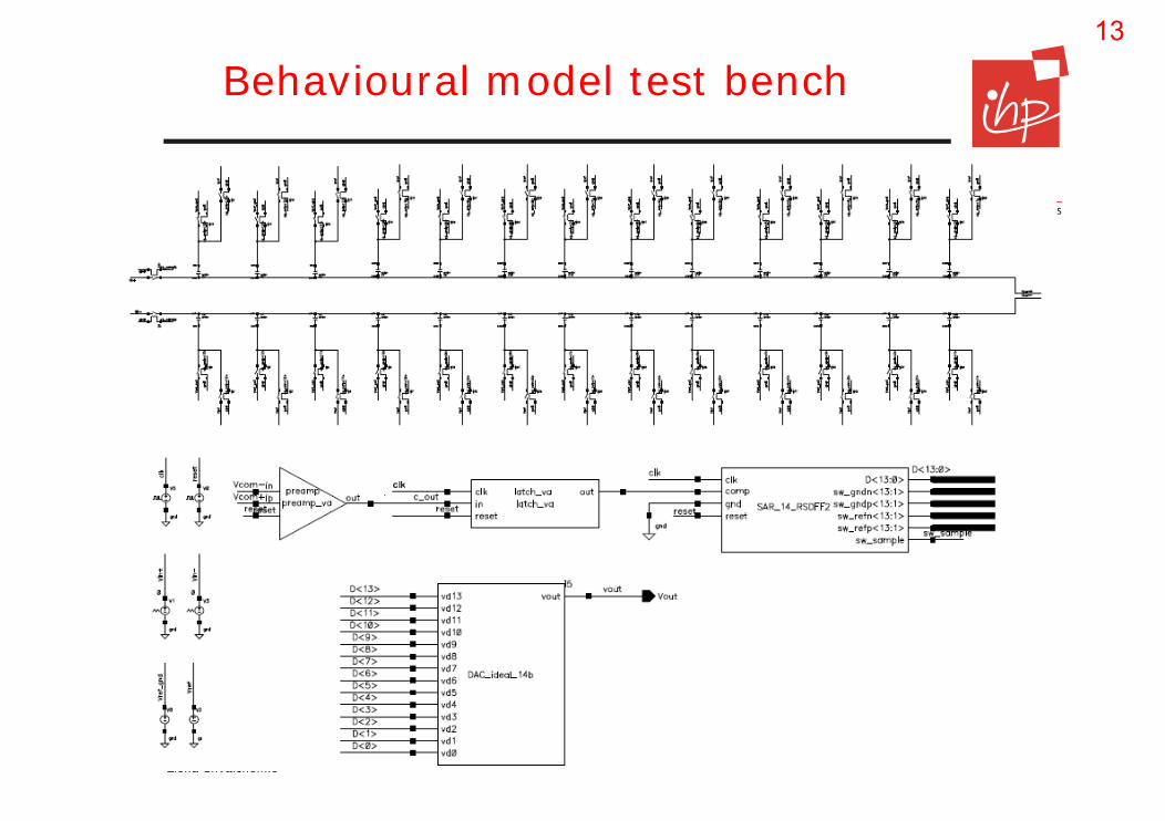
Behavioural model test bench
14
IHP Im Technologiepark 25 15236 Frankfurt (Oder) Germany www.ihp-microelectronics.com © 2011 - All rights reservedElena Shvaichenko
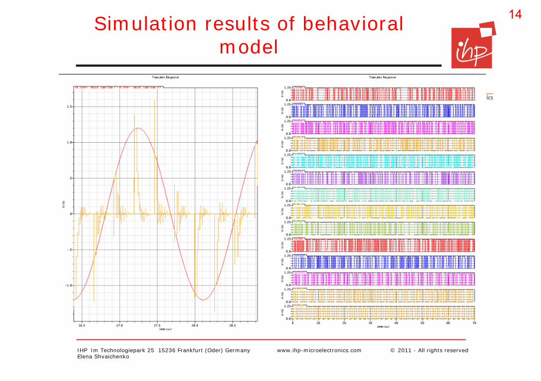
Simulation results of behavioralmodel
15
IHP Im Technologiepark 25 15236 Frankfurt (Oder) Germany www.ihp-microelectronics.com © 2011 - All rights reservedElena Shvaichenko
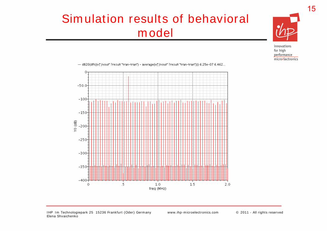
Simulation results of behavioralmodel
16
IHP Im Technologiepark 25 15236 Frankfurt (Oder) Germany www.ihp-microelectronics.com © 2011 - All rights reservedElena Shvaichenko
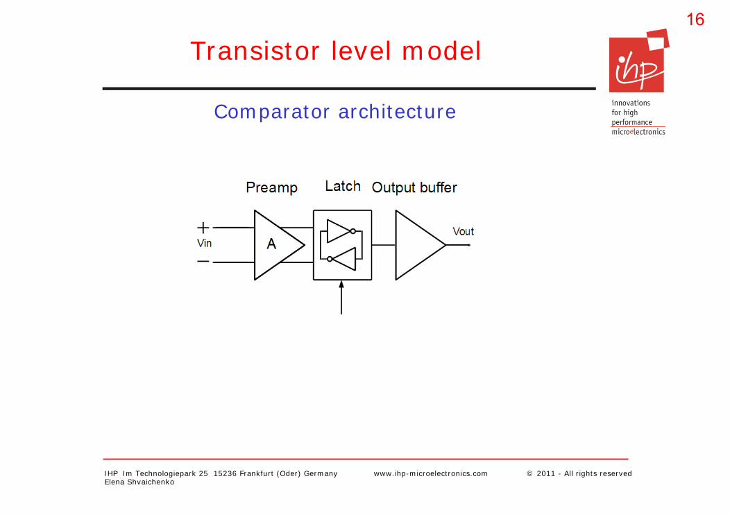
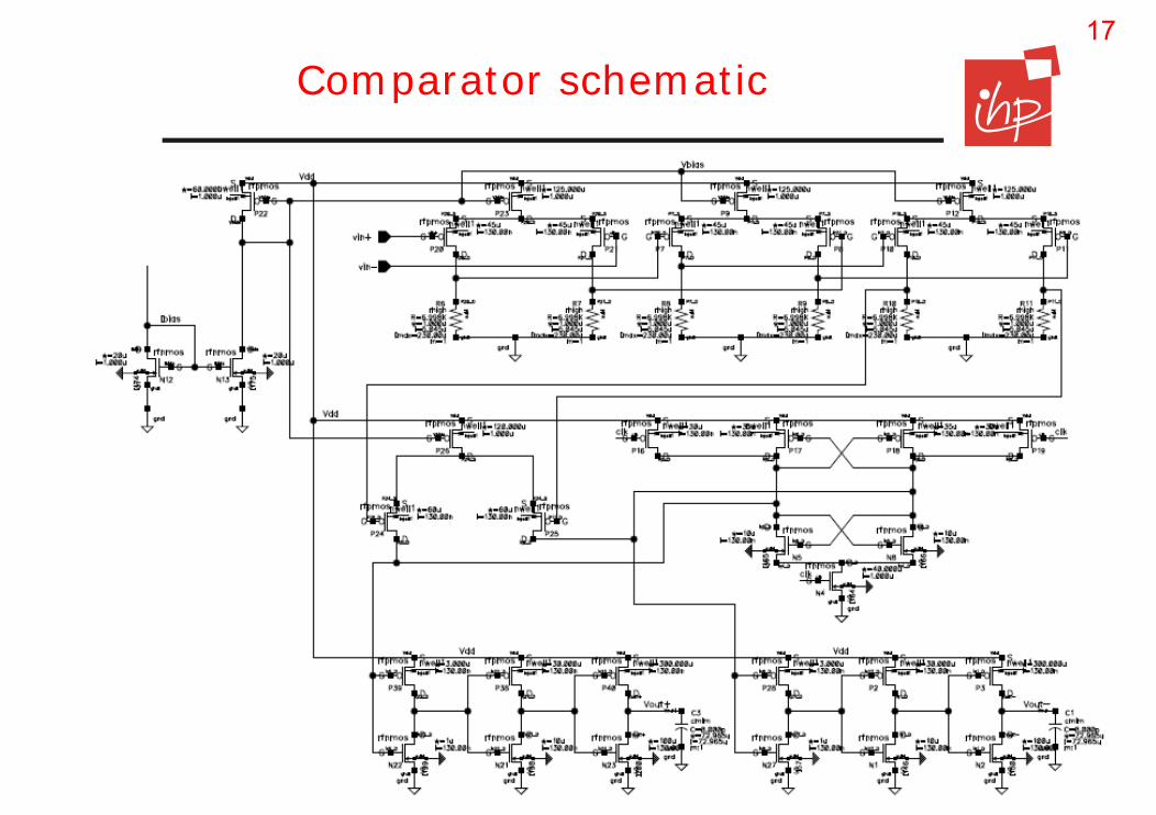
Transistor level model
Comparator architecture
17
IHP Im Technologiepark 25 15236 Frankfurt (Oder) Germany www.ihp-microelectronics.com © 2011 - All rights reservedElena Shvaichenko
Comparator schematic
18
IHP Im Technologiepark 25 15236 Frankfurt (Oder) Germany www.ihp-microelectronics.com © 2011 - All rights reservedElena Shvaichenko
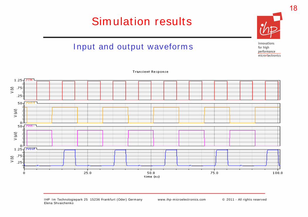
Simulation results
Input and output waveforms
19
IHP Im Technologiepark 25 15236 Frankfurt (Oder) Germany www.ihp-microelectronics.com © 2011 - All rights reservedElena Shvaichenko
Conclusion
Analysis of ADC architectures was done.
SAR architecture was chosen as most appropriate architecture to meet
given specification.
Development of program for modeling successive-approximation analog-to-digital conversion in MATLAB was done.
Analysis of non–ideal effects in SAR ADC was done.
Modeling of mismatch, input referred dc offset and settling time effects was done.
Simulation of modeling mismatch effect shows that for SG013S IHP technology it is possible to get DNL ≤ 0.5 LSB, INL < 0.5 LSB, THD = -95.07 dB, SFDR = 85.75 dB, SINAD =84.84 dB, ENOB = 13.8 bit with probability 99.7%.
Simulation of modeling comparator offset voltage effect shows that for SG013S IHP technology with 3.2 mV input referred dc offset it is possible to get THD = -84.33 dB, SFDR = 76.10 dB, SINAD =74.95 dB, ENOB = 12.16 bit with probability 99.7%.
20
IHP Im Technologiepark 25 15236 Frankfurt (Oder) Germany www.ihp-microelectronics.com © 2011 - All rights reservedElena Shvaichenko
Conclusion
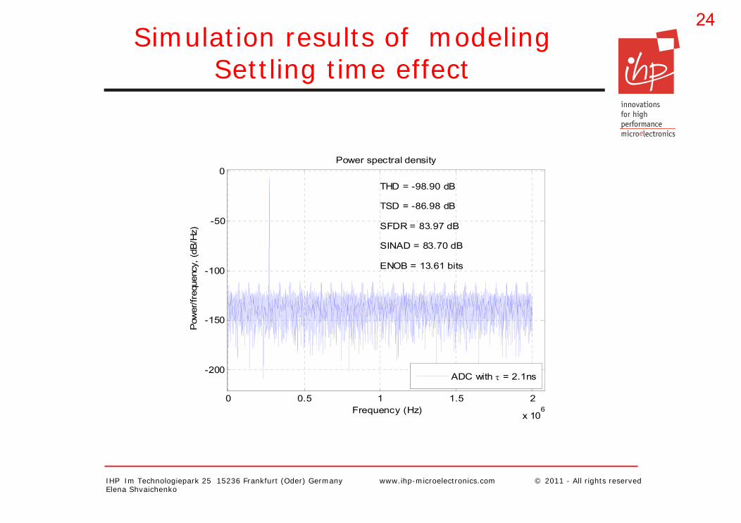
Simulation of modeling settling time effect shows that for SG013S IHP technology with 2.1 ns time constant it is possible to get SFDR = 83.97 dB, SINAD =83.7 dB, ENOB = 13.61 bit with probability 99.7%.
Verilog–A behavioral model of 14-bit differential charge–redistribution SAR ADC with monotonic switching procedure was developed.
Simulation of proposed high-speed comparator with resolution 40uV, clock frequency 100 MHz, supply voltage 1.2 V in SG013S IHP technology was done.
Analysis of more than 45 scientific sources up to 2011 year in the field of analog-to-digital conversion has been conducted.
Results of investigation have been published at the International conference on system analysis and information technologies.
The investigation was carried out for IHP - Innovations for High Performance Microelectronics company.
21
IHP Im Technologiepark 25 15236 Frankfurt (Oder) Germany www.ihp-microelectronics.com © 2011 - All rights reservedElena Shvaichenko
Thank You!!!
22
IHP Im Technologiepark 25 15236 Frankfurt (Oder) Germany www.ihp-microelectronics.com © 2011 - All rights reservedElena Shvaichenko
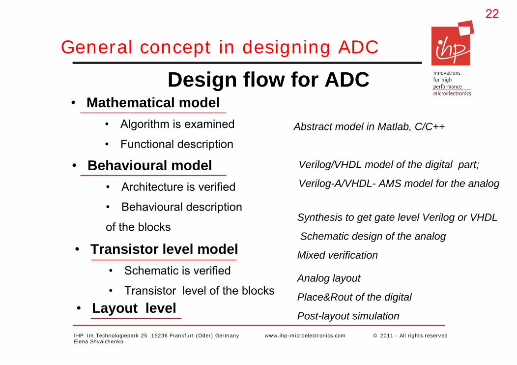
General concept in designing ADC
Design flow for ADC• Mathematical model
• Algorithm is examined
• Functional description
• Behavioural model• Architecture is verified
• Behavioural description
of the blocks
• Transistor level model• Schematic is verified
• Transistor level of the blocks• Layout level
Abstract model in Matlab, C/C++
Verilog/VHDL model of the digital part;
Verilog-A/VHDL- AMS model for the analog
Synthesis to get gate level Verilog or VHDL
Schematic design of the analog
Mixed verification
Analog layout
Place&Rout of the digital
Post-layout simulation
23
IHP Im Technologiepark 25 15236 Frankfurt (Oder) Germany www.ihp-microelectronics.com © 2011 - All rights reservedElena Shvaichenko
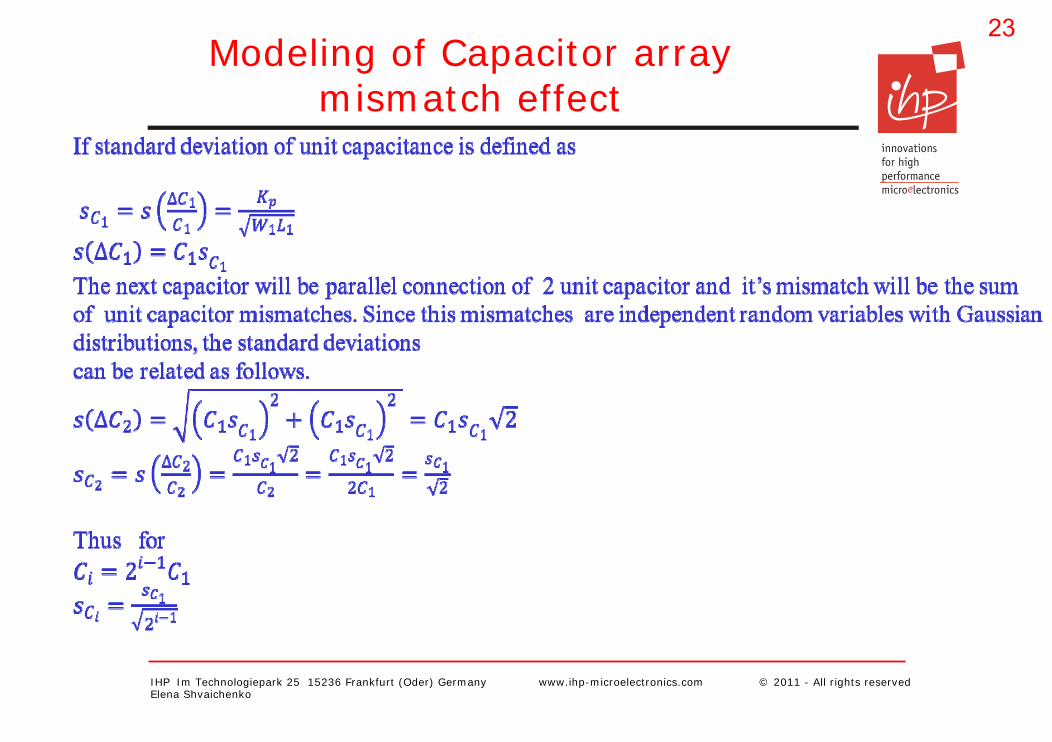
Modeling of Capacitor array mismatch effect
24
IHP Im Technologiepark 25 15236 Frankfurt (Oder) Germany www.ihp-microelectronics.com © 2011 - All rights reservedElena Shvaichenko
Simulation results of modeling Settling time effect
0 0.5 1 1.5 2
x 106
-200
-150
-100
-50
0Power spectral density
Frequency (Hz)
Pow
er/fr
eque
ncy,
(dB
/Hz)
THD = -98.90 dB
TSD = -86.98 dB
SFDR = 83.97 dB
SINAD = 83.70 dB
ENOB = 13.61 bits
ADC with τ = 2.1ns
25
IHP Im Technologiepark 25 15236 Frankfurt (Oder) Germany www.ihp-microelectronics.com © 2011 - All rights reservedElena Shvaichenko
Waveforms of conventional and monotonic switching procedure
26
IHP Im Technologiepark 25 15236 Frankfurt (Oder) Germany www.ihp-microelectronics.com © 2011 - All rights reservedElena Shvaichenko
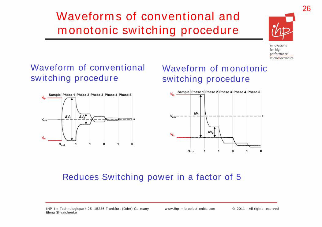
Waveforms of conventional and monotonic switching procedure
Waveform of monotonic switching procedure
Reduces Switching power in a factor of 5
Waveform of conventional switching procedure
27
IHP Im Technologiepark 25 15236 Frankfurt (Oder) Germany www.ihp-microelectronics.com © 2011 - All rights reservedElena Shvaichenko
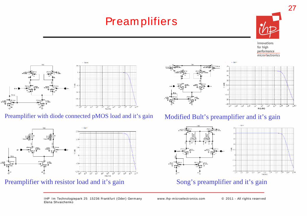
Preamplifiers
Preamplifier with diode connected pMOS load and it’s gain
Preamplifier with resistor load and it’s gain
Modified Bult’s preamplifier and it’s gain
Song’s preamplifier and it’s gain
28
IHP Im Technologiepark 25 15236 Frankfurt (Oder) Germany www.ihp-microelectronics.com © 2011 - All rights reservedElena Shvaichenko
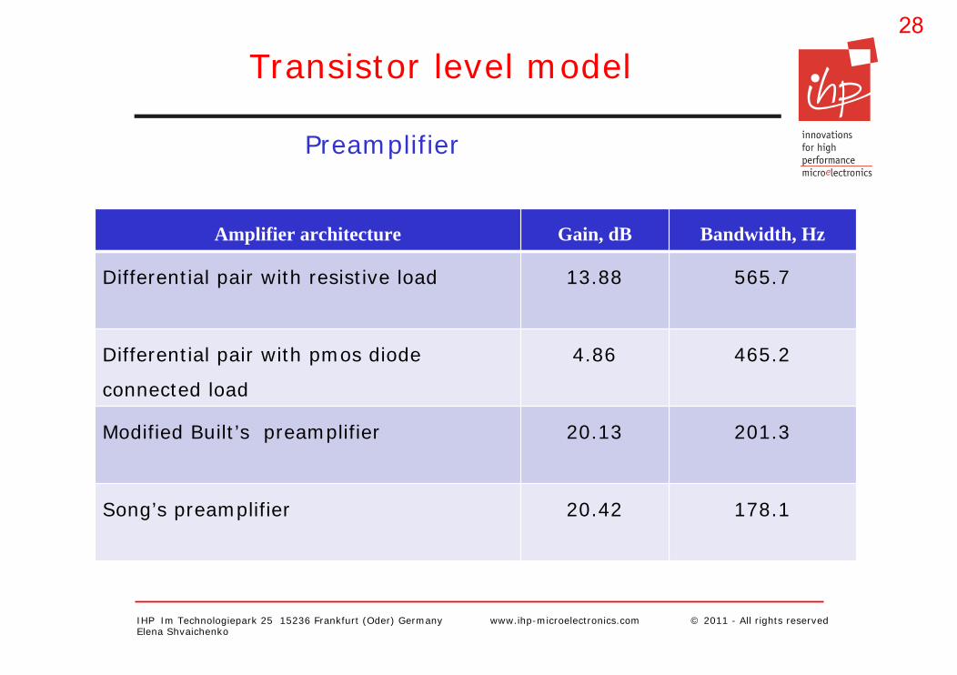
Transistor level model
Preamplifier
Amplifier architecture Gain, dB Bandwidth, Hz
Differential pair with resistive load 13.88 565.7
Differential pair with pmos diode
connected load
4.86 465.2
Modified Built’s preamplifier 20.13 201.3
Song’s preamplifier 20.42 178.1
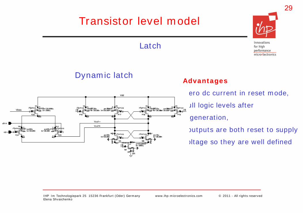
29
IHP Im Technologiepark 25 15236 Frankfurt (Oder) Germany www.ihp-microelectronics.com © 2011 - All rights reservedElena Shvaichenko
Transistor level model
Latch
Dynamic latchAdvantages
•zero dc current in reset mode,
•full logic levels after
regeneration,
• outputs are both reset to supply
voltage so they are well defined