metamaterial and metastructural architectures for novel ... · metamaterial and metastructural...
TRANSCRIPT

ARL-TR-7252 ● MAR 2015
US Army Research Laboratory
Metamaterial and Metastructural Architectures for Novel C4ISR Devices and Sensors
by Weimin Zhou, Gerard Dang, Monica Taysing-Lara, Daniel Shreiber, Melanie Cole, Eric Ngo, Matt Ivill, Grace Metcalfe, Nathaniel Woodward, and Amir Zaghloul Approved for public release; distribution unlimited.

NOTICES
Disclaimers
The findings in this report are not to be construed as an official Department of the
Army position unless so designated by other authorized documents.
Citation of manufacturer’s or trade names does not constitute an official
endorsement or approval of the use thereof.
Destroy this report when it is no longer needed. Do not return it to the originator.

ARL-TR-7252 ● MAR 2015
US Army Research Laboratory
Metamaterial and Metastructural Architectures for Novel C4ISR Devices and Sensors
by Weimin Zhou, Gerard Dang, Monica Taysing-Lara, Grace Metcalfe, Nathaniel Woodward, and Amir Zaghloul Sensors and Electron Devices Directorate
Daniel Shreiber Oak Ridge Institute for Science and Education Belcamp, MD
Melanie Cole, Eric Ngo, and Matt Ivill Weapons and Materials Research Directorate
Approved for public release; distribution unlimited.
FOR OFFICIAL USE ONLY (delete if not FOUO)

ii
REPORT DOCUMENTATION PAGE Form Approved
OMB No. 0704-0188 Public reporting burden for this collection of information is estimated to average 1 hour per response, including the time for reviewing instructions, searching existing data sources, gathering and maintaining the
data needed, and completing and reviewing the collection information. Send comments regarding this burden estimate or any other aspect of this collection of information, including suggestions for reducing the
burden, to Department of Defense, Washington Headquarters Services, Directorate for Information Operations and Reports (0704-0188), 1215 Jefferson Davis Highway, Suite 1204, Arlington, VA 22202-4302.
Respondents should be aware that notwithstanding any other provision of law, no person shall be subject to any penalty for failing to comply with a collection of information if it does not display a currently
valid OMB control number.
PLEASE DO NOT RETURN YOUR FORM TO THE ABOVE ADDRESS.
1. REPORT DATE (DD-MM-YYYY)
March 2015
2. REPORT TYPE
DSI
3. DATES COVERED (From - To)
2012–2014
4. TITLE AND SUBTITLE
Metamaterial and Metastructural Architectures for Novel C4ISR Devices and
Sensors
5a. CONTRACT NUMBER
5b. GRANT NUMBER
5c. PROGRAM ELEMENT NUMBER
6. AUTHOR(S)
Weimin Zhou, Gerard Dang, Monica Taysing-Lara, Daniel Shreiber, Melanie
Cole, Eric Ngo, Matt Ivill, Grace Metcalfe, Nathaniel Woodward, and Amir
Zaghloul
5d. PROJECT NUMBER
5e. TASK NUMBER
5f. WORK UNIT NUMBER
7. PERFORMING ORGANIZATION NAME(S) AND ADDRESS(ES)
US Army Research Laboratory
ATTN: RDRL-SEE-E
2800 Powder Mill Road
Adelphi, MD 20783-1197
8. PERFORMING ORGANIZATION REPORT NUMBER
ARL-TR-7252
9. SPONSORING/MONITORING AGENCY NAME(S) AND ADDRESS(ES)
10. SPONSOR/MONITOR'S ACRONYM(S)
11. SPONSOR/MONITOR'S REPORT NUMBER(S)
12. DISTRIBUTION/AVAILABILITY STATEMENT
Approved for public release; distribution unlimited.
13. SUPPLEMENTARY NOTES
14. ABSTRACT
We have developed novel metamaterial devices and metastructures with new electronic and optoelectronic (OE) properties
and used them to design and fabricate devices, such as slow-light, low-loss waveguides, terahertz modulators, and wideband
radio frequency (RF) antennas with new functionalities. These devices will provide basic building blocks for future chip-scale
semiconductor-integrated OE circuits and provide new capabilities over a wide range of frequencies from microwaves,
terahertz, and into the infrared in Command, Control, Communications, Computers, Intelligence, Surveillance and
Reconnaissance systems. We focused on 3 different types of metamaterial devices as basic building blocks. These are low-
loss, slow-light, hollow-core metastructure waveguides for chip-scale-integrated OE/RF photonic circuit; metamaterial
devices for terahertz communication/sensing/imaging; and tunable RF metamaterials. Some of our major accomplishments in
this area of study include developing and demonstrating the world’s first silicon-based slow-light metastructure hollow-core
waveguide, developing and demonstrating new tunable terahertz metamaterial devices, and designing and fabricating terahertz
metastructure hollow-core waveguide. The DSI project has resulted in 14 publications, 1 US patent, 1 invention disclosure,
and 1 press release. 15. SUBJECT TERMS
metamaterial, metastructure, devices, terahertz, hollow-core waveguide
16. SECURITY CLASSIFICATION OF: 17. LIMITATION OF ABSTRACT
UU
18. NUMBER OF PAGES
76
19a. NAME OF RESPONSIBLE PERSON
Weimin Zhou
a. REPORT
Unclassified
b. ABSTRACT
Unclassified
c. THIS PAGE
Unclassified
19b. TELEPHONE NUMBER (Include area code)
301-394-1435 Standard Form 298 (Rev. 8/98)
Prescribed by ANSI Std. Z39.18

iii
Contents
List of Figures v
Acknowledgments ix
1. Introduction 1
1.1 Objective 1
1.2 Approach 1
1.3 Major Accomplishments 2
2. Slow-Light High-Contrast Metastructure Hollow-Core Waveguide 3
2.1 Abstract 3
2.2 Introduction 3
2.3 Modeling and Simulation 5
2.4 Design and Fabrication 7
2.4.1 Fabrication Methods 8
2.4.2 Comparison 9
2.4.3 Expansion for Terahertz Waveguide Fabrication 11
2.5 Experimental Test Results 12
2.5.1 Waveguide Guiding Test 12
2.5.2 Waveguide Propagation Loss Measurement 12
2.5.3 Group Velocity Measurement 15
2.6 Discussion 17
2.7 Conclusion 18
2.8 References 19
3. Design and Fabrication of 3-dimensional (3-D) High-Contrast Metastructure Terahertz Cage Waveguides 20
3.1 Abstract 20
3.2 Introduction 20
3.3 Waveguide and Fabrication Designs 21
3.3.1 Waveguide Design and Simulation 21
3.3.2 Fabrication Technique 23

iv
3.4 Fabrication 24
3.4.1 Undercutting Etch to Form the Waveguide Hollow Core 24
3.4.2 Deep Through-Wafer Etch to Form the Waveguide’s High-Contrast-Grating (HCG) Metastructure Cladding 27
3.5 Conclusion 29
3.6 References 30
4. Tunable Terahertz Metamaterial Devices 31
4.1 Abstract 31
4.2 Introduction 31
4.3 Design, Modeling, and Simulation 32
4.4 Fabrication 36
4.4.1 Develop Fabrication Technique 36
4.4.2 BST Thin Film Growth 36
4.4.3 Bias metal lines 37
4.4.4 3-D Split-Ring Fabrication 38
4.4.5 Device Characterization and Test 39
4.6 Terahertz Transparent Electrode Study 42
4.7 Conclusion 43
5. Radio Frequency Metamaterial Research 44
5.1 Capacitively Loaded Loop/Probe (CLL-P) Cell 44
5.2 Random Capacitively Loaded Loop/Probe (CLL-P) Arrangement 50
5.3 Measurements of CLL-P Metamaterial Slabs 52
5.4 Remarks on Metamaterial Characterization 56
5.5 Application of CLL Metamaterials to Dipole Antenna Enhancement 56
5.6 References 59
6. List of Publications, Patents, and Papers 61
Distribution List 64

v
List of Figures
Fig. 2.1 Representation of the meta-HCG 3-D cage hollow-core waveguide structure ................................................................................................4
Fig. 2.2 Simulation modeling: the mode hopping due to the phase transition at the meta-HCG causes a flat slope on the dispersion curve, which represents a low group velocity ............................................................6
Fig. 2.3 Simulation of a 1-µm core metastructure hollow-core waveguide ......6
Fig. 2.4 Simulated “slow light” with average 0.02c velocity and 0.1 dB/cm loss over a 100-GHz bandwidth ...........................................................7
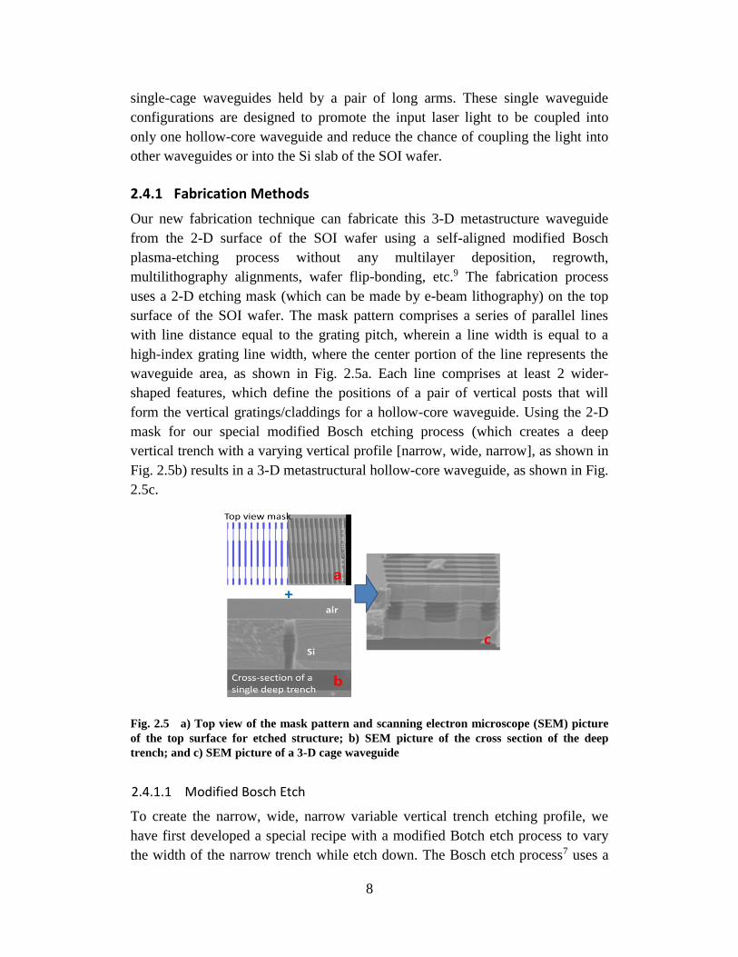
Fig. 2.5 a) Top view of the mask pattern and scanning electron microscope (SEM) picture of the top surface for etched structure; b) SEM picture of the cross section of the deep trench; and c) SEM picture of a 3-D cage waveguide ....................................................................................8
Fig. 2.6 SEM pictures of the metastructure cage waveguides of core size ~2 µm, HCG high 1.5 µm, period 627 nm in a) 5-waveguide array configuration; b) single waveguide supported by short arms; and c) single waveguide supported by long arms .........................................10
Fig. 2.7 The SEM pictures of the fabricated metastructure cage waveguide a) before and b) after the thermal oxidization and HF etching process ..10
Fig. 2.8 Block diagram of the waveguide test setup ........................................12
Fig. 2.9 Transmission curve averages of our waveguide for 3 different waveguide lengths ..............................................................................14
Fig. 2.10 Average propagation loss curve for our waveguide ...........................14
Fig. 2.11 Block diagram of the group velocity (waveguide delay) measurement setup ....................................................................................................15
Fig. 2.12 Transmitted pulses from the oscilloscope with (blue) and without (red) the waveguide. For comparison, reference pulse intensity is multiplied by a factor of 2 (green) for normalization. Comparing the 2 pulse positions, there is a delay of about 200 ns of the pulse passing through the waveguide. ......................................................................16
Fig. 2.13 Plot of the pulse peak position as a function of time for a pulse transmitted from a waveguide with short-arm support (blue), long-arm waveguide (green), and the reference pulse (red) .......................16
Fig. 3.1 Two- and three-dimensional cross-sectional diagrams of the terahertz hollow-core waveguide with high-contrast gratings. The axis for waveguiding is into the center of the cylindrical hollow core. ..........21
Fig. 3.2 a) Dispersion relation diagram of our 3-D waveguide. b) Mode pattern of the fundamental mode in our 3-D waveguide. ...................22

vi
Fig. 3.3 The excitation of a 10-ps pulse and subsequent decay of the waveguide mode. Slope of the decaying is proportional to the waveguide loss. ..................................................................................23
Fig. 3.4 Truncated .gds layout of overlaid mask levels. This would translate to a top view of the fabricated waveguide. The small boxes between the waveguides are alignment marks. .....................................................24
Fig. 3.5 Scanning electron microscope (SEM) image of wafer surface after the top-oxide etch. Dry-etching was used and some etching of the silicon occurred to ensure complete removal of the silicon dioxide. The photoresist mask was removed for the SEM image...................25
Fig. 3.6 SEM image showing the initial trench etch for reaching the center of the wafer prior to the hollow-core etch. A line can be seen in the trench because 2 separate Bosch etches were performed to achieve the desired depth. ..............................................................................26
Fig. 3.7 SEM image showing the hollow-core etch in the wafer and the etched spheres punching through to adjacent spheres. The surface of the sample used for this image shows damage from the scribe because a continuous cleaving plane does not exist after the hollow core is formed. ..................................................................................27
Fig. 3.8 Cross-sectional SEM images of the waveguides. (Top) An SiO2 shell in the shape of the first trench etched can be seen at the top of the hollow core. (Bottom) The SiO2 shell in the core was removed by buffered high-frequency etch. ...........................................................28
Fig. 3.9 SEM images of the waveguides after etching in CR-9 and buffered oxide etchant .....................................................................................29
Fig. 4.1a Tunable 3-D terahertz metamaterial unit cell. (Left) Cross section of the split-ring unit cell with complex oxide film as tunable capacitor (right) and (right inset) scanning electron microscopy (SEM) picture.33
Fig. 4.1b 3-D illustration of the tunable metamaterial .....................................33
Fig. 4.2 HFSS model simulation of the test surfaces showing the resonant frequency and some nonresonant energy dissipation........................33
Fig. 4.3 (Left) Time-resolved terahertz transmission spectroscopy data and (right) complex refractive index of a polyimide thin film on sapphire34
Fig. 4.4 Results from the HFSS model of the designed and implemented metamaterial surface. The location of the resonance peak is accurately predicted with assumed value of BST dielectric constant.35
Fig. 4.5 HFSS model of the metamaterial device when BST thin film is assumed to have a dielectric constant of 170 (blue) and 180 (red). The 1-GHz leftward shift is analogues to the 4-V bias applied to the device (experimental data). ...............................................................36
Fig. 4.6 (Left) Atomic Force Microscopy (AFM) image and (right) X-ray diffraction (XRD) image of BST thin film grown on sapphire substrate ............................................................................................37
vii
Fig. 4.7 Top and bottom electrode .................................................................37
Fig. 4.8 Left: microscope picture of the split-ring arrays focused on the bottom tunable capacitor with metal contact line; Right: 3-D optical microscope picture of the split-ring metamaterial device .................39
Fig. 4.9 Polarized terahertz transmission through SRR structures .................39
Fig. 4.10 Schematics of the experimental setup for WMRD’s terahertz time-domain spectrometer .........................................................................40
Fig. 4.11 Resonant peak shift when the bias of 0, 2, and 6 V is applied to active metamaterial in time-domain terahertz spectrometer. The inset shows a 2-GHz shift in resonance frequency when a 6-V bias is applied. ..............................................................................................41
Fig. 4.12 SEM of THz metamaterial unit cell with unfilled “capacitor gap”. The schematics of the structure are provided in Fig. 4.1. ...............42
Fig. 4.13 Transmission terahertz spectroscopy of ITO ....................................42
Fig. 5.1 a) Capactively loaded loop (CLL) and b) CLL plus probe (CLL-P) unit cells in parallel orientations .......................................................45
Fig. 5.2 CLL plus probe (CLL-P) unit cells in perpendicular orientation .....45
Fig. 5.3 S parameters, magnitude, and phase for CLL cells without probes: parallel orientation ............................................................................47
Fig. 5.4 Material impedance, refractive index, permittivity, and permeability for CLL cells without probes: parallel orientation ............................47
Fig. 5.5 S parameters, magnitude, and phase for CLL cells with probes of cut wires: parallel orientation .................................................................48
Fig. 5.6 Material impedance, refractive index, permittivity, and permeability for CLL cells with probes of cut wires: parallel orientation .............48
Fig. 5.7 S parameters, magnitude, and phase for CLL cells with probes of continuous wires: parallel orientation ...............................................49
Fig. 5.8 Material impedance, refractive index, permittivity, and permeability for CLL cells with probes of continuous wires: parallel orientation 49
Fig. 5.9 S parameters, magnitude, and phase for CLL cells with probes of continuous wires: perpendicular orientation .....................................50
Fig. 5.10 Material impedance, refractive index, permittivity, and permeability for CLL cells with probes of continuous wires: perpendicular orientation .........................................................................................50
Fig. 5.11 Three-dimensional random arrangement of CLL cells .....................51
Fig. 5.12 Two-dimensional random arrangement of CLL cells forming a slab: (left) top view of one layer and (right) side view showing 2-D layers52
Fig. 5.13 Magnitude (left) and phase (right) of S11 (red) and S21 (blue) for a layered 2-D random metamaterial of CLL-P cells ............................52

viii
Fig. 5.14 Unit cell of fabricated CLL-P periodic (left) and random (right) metamaterial with cut wire probes ....................................................53
Fig. 5.15 Picture of fabricated CLL-P metamaterial in periodic (top) and 3-D random arrangements ........................................................................53
Fig. 5.16 Sketch of the measurement setup to study the transmission, reflection, and refraction performance of the metamaterial slab for boresight and inclined incidence .......................................................54
Fig. 5.17 Picture of the measurement setup designed with optional upper plate for parallel-plate waveguide transmission ........................................54
Fig. 5.18 Refractive index for periodic and random structures as deduced from measured transmission and refraction phases ...................................55
Fig. 5.19 Transmission parameter S21 for periodic and random slabs, showing the shift in bandwidth........................................................................55
Fig. 5.20 Metamaterial-enhanced dipole using multiple planes of CLL cells and sharp high-gain beam .................................................................57
Fig. 5.21 Picture of fabricated planar structure for metamaterial-enhanced dipole.................................................................................................57
Fig. 5.22 Simulated and measured S11 of the planar metamaterial-enhanced dipole.................................................................................................58
Fig. 5.23 Comparison of measured (green and black) vs. simulated (orange and dashed blue) realized gain and front-to-back ratio of planar metamaterial-enhanced dipole; conventional dipole is also plotted as a reference (dotted red) .....................................................................58

ix
Acknowledgments
We acknowledge our university collaborators, Prof Connie Chang-Hasnain, Dr
Vadim Karagodsky, Tianbo Sun, and Dr Weijian Yang from the University of
California at Berkeley, and Dr Phillippe Lalanne from Institut d’Optique (France)
for their contribution of theoretical modelling and simulation for the metastructure
hollow-core waveguides.
We thank Dr Larry Stout, Dr Steve Weiss, and Dr Mike Wraback for their
administrative guidance.

x
INTENTIONALLY LEFT BLANK.

1
1. Introduction
1.1 Objective
Our objective for this research is to develop novel metamaterial devices and
metastructures with new electronic and optoelectronic (OE) properties and use
them to design and fabricate devices, such as slow-light, low-loss waveguides,
terahertz modulators, and wideband radio frequency (RF) antennas with new
functionalities. These devices will provide basic building blocks for future chip-
scale semiconductor-integrated OE circuits and provide new capabilities over a
wide range of frequencies from microwaves, terahertz, and into the infrared in
Command, Control, Communications, Computers, Intelligence, Surveillance, and
Reconnaissance (C4ISR) systems.
1.2 Approach
We are focusing on 3 different types of metamaterial devices as basic building
blocks:
Low-loss, slow-light, hollow-core metastructure waveguides for chip-
scale-integrated OE/RF photonic circuits (EO&P, SEDD). We will use a
new type of high-contrast-grating metastructure as “cage”-cladding of a
hollow-core waveguide structure to achieve low propagation loss and
“slow-light” properties. This can provide a long time delay or an ultra-
high Q cavity in a small semiconductor chip.
Metamaterial devices for terahertz communication/sensing/imaging
(SEDD and WMRD). We will develop an active metamaterial device to
control polarization or intensity in the terahertz regime. The active
metamaterial is constructed using split-ring resonator unit cells as
canonical elements with a tunable capacitor made by complex oxide thin
films or photoelectric materials. This device will provide the basic
building blocks for future terahertz communication/sensing/imaging
applications.
Tunable RF metamaterials (RF&E, SEDD). We will design and
characterize tunable metamaterials at RF frequencies through simulations
and measurements.

2
1.3 Major Accomplishments
Some of our major accomplishments in this area of study are as follows:
Developed and demonstrated the world’s first silicon (Si)-based slow-light
metastructure hollow-core waveguide. We have designed, fabricated, and
tested this new type of 3-dimensional (3-D) cage-like metastructure
waveguide. As a result, a new and unique fabrication technique was
developed in-house. We have experimentally tested several fabricated
waveguides to measure the propagation loss and group velocity. We
demonstrated propagation losses less than 1 dB/cm at certain wavelengths
and a group velocity greater than 0.2c, where c is the speed of light, for
slow-light propagation. In collaborating with UC Berkeley and Institute
d’Optique (France), we developed a simulation model for this waveguide.
Developed and demonstrated new tunable terahertz metamaterial devices.
We have designed several tunable terahertz metamaterial structures
containing 3-D metal split-rings with a tunable capacitor fabricated using
complex oxide thin films. Subsequently, the team developed a new
fabrication technique and successfully fabricated such 3-D tunable
metamaterial devices. In addition, a simulation model is developed to
assist the metamaterial device design and predict the resonance frequency
and tuning. We have finally tested a fabricated device sample in terahertz
frequency. The test result is in general agreement with the experimental
test.
Designed and fabricated terahertz metastructure hollow-core waveguide.
We have successfully designed and fabricated the world’s first Si-based
metastructure hollow-core waveguide. The waveguide is built using the
entire wafer thickness. The waveguides have a round cross-sectional
hollow core surrounded by highly reflective cladding walls, which is made
by high-contrast metastructure gratings. We developed a new fabrication
technique to fabricate such a 3-D metastructure cage-like waveguide
structure. The waveguide is aimed for low propagation loss and
integration with Si-based integrated circuits for the application in terahertz
circuitry for bio/chem sensing or terahertz imaging.
The DSI project has resulted in 14 publications, 1 US patent, 1 invention
disclosure, and 1 press release.
3
2. Slow-Light High-Contrast Metastructure Hollow-Core Waveguide
Gerard Dang, Monica Taysing-Lara, and Weimin Zhou (SEDD)
2.1 Abstract
We have developed a new type of silicon (Si)-based 3-dimensional (3-D) cage-
like high-contrast metastructure waveguide with both “slow-light” and low-loss
properties, which has applications in providing a long time-delay line or a high Q
cavity in chip-scale optoelectronic integrated circuits (OEICs). Traditional
semiconductor optical waveguides always have high loss when used in a high-
dispersion (slow-light) region. A preliminary computational model has predicted
that there is a slow-light and low-propagation loss region within cage-like hollow-
core waveguides formed by 4 high-contrast-grating (HCG) walls/claddings. Using
our new processing technique, we fabricated several such waveguides on an Si
wafer with different core sizes/shapes and different HCGs for 1,550 operation
wavelength. We have conducted experimental waveguide delay test
measurements using a short optical pulse which indicated that the group velocity
of these metastructure waveguides are in the range of 20%–30% of the speed of
the light. Using a waveguide “cut-back” method, we have experimentally
determined the propagation loss of these waveguides is in the range of 2–5
dB/cm. We are also developing this type of high-contrast metastructure hollow-
core waveguide for different operating wavelengths/frequencies, such as terahertz,
for different applications.
2.2 Introduction
Semiconductor integrated circuits (ICs) and fiber optics are the 2 basic
technologies that have made a big impact in our modern lives. In many cases,
low-loss long fiber has been used not for sending signals over long physical
distances, but rather for providing a long time delay or an ultra-high Q cavity.
Unfortunately, long fiber spools are large in size and cannot be monolithically
integrated with semiconductor IC. If we can create a slow-light, low-loss
waveguide with a small form factor on an Si wafer, we can then provide a long
time delay or an ultra-high Q cavity in a chip scale digital or analog OEIC for
many applications, such as a buffered delay for communication or computation
system, precision optical or radio frequency (RF) signal sources, optical true-
time-delay beamformer for phased array antennas, RF-photonic signal

4
processors/filters, etc. “Slow-light” is the key to reducing the size of the delay
line. Unfortunately, traditional waveguides always have a high propagation loss
when used in a high-dispersion wavelength region since loss and dispersion
cannot be separated in a homogeneous material.
In recent years, UC Berkeley has found a new type of HCG metastructure that has
demonstrated ultra-high reflectivity.1,2 Therefore, using this type of metagrating
as the wall/cladding to build a hollow-core waveguide, as shown in Fig. 2.1, can
achieve ultra-low loss because the propagation light cannot escape from the HCG
cladding, and there is no absorption loss in the core area.3–5 The physics of this
metagrating are related to resonance created by the artificial unit cell or the
geometric arrangement of 2 materials having a high index contrast. This provides
us with an opportunity to engineer the HCG metastructure to create a “bending”
in the -k dispersion curve for the propagation modes in the waveguide. The
“bending” causes a “0” slope region in the dispersion curve (“0” group velocity).
The challenge is to design the waveguide such that it has both slow-light and low-
loss properties in the same operational bandwidth. Hence, such a slow-light
waveguide device will be very useful for RF-photonics applications, such as delay
lines or building a high-Q-cavity microwave.
Fig. 2.1 Representation of the meta-HCG 3-D cage hollow-core waveguide structure
The next challenge is to fabricate such a 3-D cage-structure waveguide. Recently,
the RF-Photonics team at the US Army Research Laboratory developed a new
low-cost fabrication technique to construct the 3-D cage hollow-core waveguide
that has HCG metastructures as the 4 cladding/walls of the waveguide,4,6 all
fabricated on a standard Si-on-insulator (SOI) wafer.
In this project, we have to first improve our fabrication technique to reduce the
roughness and nonuniformity size variation by comparing and testing different
etching techniques, such as modified Bosch etch4,7 and modified Bosch with
isotropic under-cut etch.8 Since the simplified 2-dimensional (2-D) ideal
computation model cannot precisely predict the real case for the 3-D cage-
structure waveguide, we had to fabricate several waveguides with different core

5
sizes/shapes and different HCGs for 1,550 operation wavelength. We have
conducted an experimental waveguide delay test using a short optical pulse to
measure the group velocity and demonstrate the slow-light property. Using a
waveguide “cut-back” method, we have experimentally determined the
propagation loss of these waveguides.
2.3 Modeling and Simulation
The goal of this project is to develop the hollow-core waveguide not only for low
loss, but also for high dispersion or “slow-light” properties. To design such a
waveguide, as shown in Fig. 2.1 we use high-reflection HCG metastructures as the
4 cladding/walls of a squared hollow-core waveguide, where the guided light is
approximately 100% reflected from the metagratings, and there is no absorption
from the core, therefore resulting in ultra-low loss. Unlike a conventional
waveguide, a metastructural waveguide can be engineered to create a phase
transition that generates a “0” slope in the dispersion curve (i.e., “0” group
velocity). We chose Si-base SOI wafers to make our waveguide for operation
wavelength around 1,550 nm; therefore, the waveguide can be monolithically
integrated with an Si-based OE circuit and have the advantage of a complementary
metal-oxide semiconductor (CMOS)-compatible fabrication process.
We collaborated with Prof Connie Chang-Hasnain’s group at UC Berkeley to
conduct theoretical simulation and modeling to search a suitable waveguide structure
that has both low-loss and slow-light effects in the same operational bandwidth.
UC Berkeley’s research group has developed a simplified model to simulate such
a waveguide with beam propagation between 2 HCGs, as shown in Fig. 2.2. This
simplified simulation model is based on 2-D calculation of the high-contrast
grating and combining the 2-D result with the hollow-core waveguide simulation.
The black dispersion curves represent the propagation modes of a traditional
hollow-core slab waveguide with total reflection cladding. The blue curves
represent the modes of an HCG metastructure hollow-core slab waveguide. We
can see that there is a mode transition between 2 neighboring modes that has a
smaller slope. Figure 2.2 (left) shows the 2-D mapping of the computational
modeling results of the dispersion curve and loss plot (HCG’s reflectivity
showing by color) for the propagation modes in this waveguide. Figure 2.2 (right)
shows the mapping of the dispersion curves with the phase of the propagation
modes, which indicate that the mode hopping (transition) occurs at a π phase
transition. By adjusting the core dimension, D, the duty cycle, , and the height
of the grating bar, tg, one can obtain a region that has both “slow-light” (low
group velocity) and low-loss properties.

6
Fig. 2.2 Simulation modeling: the mode hopping due to the phase transition at the meta-
HCG causes a flat slope on the dispersion curve, which represents a low group velocity
Figure 2.3 shows the result for D = 1 µm, = 1.5 µm, and a duty cycle of 50/50.
Figure 2.4 (left) shows the “zoom-in” plot of the waveguide loss superimposed
with the “slow-light” region of the dispersion curve in k-space. Figure 2.4 (right)
shows both the loss and the group velocity as a function of frequency. These
preliminary modeling results indicate that the group velocity can be as low as
0.02c with very little waveguide loss; the bandwidth of this low-loss region is
about 100 GHz. This means such a slow-light waveguide device will be very
useful for RF-photonics applications, such as delay lines or building a high-Q-
cavity microwave.
Fig. 2.3 Simulation of a 1-µm core metastructure hollow-core waveguide

7
Fig. 2.4 Simulated “slow light” with average 0.02c velocity and 0.1 dB/cm loss over a 100-
GHz bandwidth
This simulation result may provide some guidance only for the hollow-core
metastructure waveguide’s property. A more complex 3-D simulation model is
needed to more precisely calculate the dispersion and waveguide loss for this new
type of waveguide. More detailed theoretical modeling and simulation will be
published elsewhere.
2.4 Design and Fabrication
The goal of this effort is to design and fabricate the metastructure hollow-core
waveguide that has both slow-light and low-loss properties. The simplified 2-D
ideal computation model for the slab waveguide formed by top and bottom HCGs
cannot precisely represent the real case for the 3-D cage-structure waveguide that
has 4 HCG walls. A more sophisticated 3-D simulation model is needed to find
the optimum slow-light and low-loss region with precise 3-D cage structure’s
HCG parameters for the 3-D waveguide. However, the simplified 2-D simulation
model can provide some hints for guidance. By adjusting the core dimension, D,
the duty cycle, , and the height of the grating bar, tg, one can see the trend of
change in the dispersion curve and loss property in the -k diagram. Using this
guidance, we have designed many of the waveguides for 1,550-nm operation with
different dimensions: core sizes D = 1 × 1 µm, 1.5 × 1 µm, 2 × 1.5 µm, and 2 × 2
µm, etc.; period from 0.625 to 0.7 µm; duty cycle from 20/80 to 50/50.
The waveguides are fabricated on SOI wafers so that they can be monolithically
integrated with an Si-base OEIC and have the advantage of a CMOS-compatible
fabrication process. The cage waveguide is made in the top Si layer. The silicon
dioxide (SiO2) layer under the waveguide region is removed to suspend the cage
waveguide. We have designed 3 configurations of the cage waveguide: 1) 5
waveguides per array so that each neighboring waveguide shares the same vertical
HCG cladding; 2) single-cage waveguides held by a pair of short arms; and 3)
8
single-cage waveguides held by a pair of long arms. These single waveguide
configurations are designed to promote the input laser light to be coupled into
only one hollow-core waveguide and reduce the chance of coupling the light into
other waveguides or into the Si slab of the SOI wafer.
2.4.1 Fabrication Methods
Our new fabrication technique can fabricate this 3-D metastructure waveguide
from the 2-D surface of the SOI wafer using a self-aligned modified Bosch
plasma-etching process without any multilayer deposition, regrowth,
multilithography alignments, wafer flip-bonding, etc.9 The fabrication process
uses a 2-D etching mask (which can be made by e-beam lithography) on the top
surface of the SOI wafer. The mask pattern comprises a series of parallel lines
with line distance equal to the grating pitch, wherein a line width is equal to a
high-index grating line width, where the center portion of the line represents the
waveguide area, as shown in Fig. 2.5a. Each line comprises at least 2 wider-
shaped features, which define the positions of a pair of vertical posts that will
form the vertical gratings/claddings for a hollow-core waveguide. Using the 2-D
mask for our special modified Bosch etching process (which creates a deep
vertical trench with a varying vertical profile [narrow, wide, narrow], as shown in
Fig. 2.5b) results in a 3-D metastructural hollow-core waveguide, as shown in Fig.
2.5c.
Fig. 2.5 a) Top view of the mask pattern and scanning electron microscope (SEM) picture
of the top surface for etched structure; b) SEM picture of the cross section of the deep
trench; and c) SEM picture of a 3-D cage waveguide
2.4.1.1 Modified Bosch Etch
To create the narrow, wide, narrow variable vertical trench etching profile, we
have first developed a special recipe with a modified Botch etch process to vary
the width of the narrow trench while etch down. The Bosch etch process7 uses a

9
repetition of 3 steps of either a plasma etch or a deposition cycle to achieve a
high-aspect ratio etch in Si with vertical sidewalls. The first step uses polymer
passivation to coat the open surface with a thin polymer coating. The second step
is a directional etch using high-energy plasma to remove the polymer that is on
the bottom of the open surfaces while maintaining a protective polymer layer on
the sidewalls of the trench. The third step is an isotropic Si etch. We modified the
standard Bosch process to achieve a wider core region in our etch profile by
adjusting the isotropic etch effect in order. This modified Bosch etch can undercut
the core region under the top HCG to form the hollow core and leave a series of
parallel vertical posts to form the vertical metagrating cladding as well as the
bottom metagrating. After the dry-etch processes, selective wet buffered hydrogen
fluoride (HF) etch is used to remove the SiO2 layer under the waveguide so that
the 3-D hollow-core waveguide is suspended in air.
2.4.1.2 Modified Bosch Etch with Isotropic Undercut Etch
We have developed an alternative etch method to create the narrow, wide, narrow
variable vertical trench etching profile, which adapted part of the Single-Crystal
silicon REactive etch and Metal (SCREAM) etch process8 in our modified Bosche
etch method. The method involves a few more steps. The first step is to use the
regular Bosch etch to etch the trench for the top HCG cladding with the same etch
mask. Then, deposit a thin coating of SiO2 on the etched trench surface using
plasma-enhanced chemical vapor deposition (PECVD) or put an additional
polymer coating. The next step is to use directional plasma etching to remove the
SiO2 coating (polymer) at the bottom of the trench, then perform another standard
Bosch etch to continue the trench by adding a waveguide core height. After that,
we use oxygen plasma to remove the polymer coating on the lower part (core
region) of the trench and perform an isotropic etching to expand the width of the
trench until it undercuts the core region completely. The next step is to repeat
another standard Bosch etch to create the bottom HCG/cladding until it reaches
the SiO2 layer of the SOI wafer. The final step is to again perform an HF wet etch
to remove the SiO2 layer under the waveguide.
2.4.2 Comparison
Figure 2.6 shows the scanning electron microscope (SEM) pictures of several
high-contrast metastructure hollow-core waveguides fabricated with the modified
Bosch method. Figure 2.6a shows a waveguide array, Fig. 2.6b shows a single
waveguide with short support arm configuration, and Fig. 2.6c shows a single
waveguide with the long-arm support. The advantage of the modified Bosch
method is the simplicity of fabrication. The fabrication can be done by a “single”

10
programmable, cycled, inductance coupled plasma (ICP) etch plus a wet etch with
HF. The problem with our modified Bosch etch technique is the scalloping
roughness on the vertical walls/posts and a needle bar in the middle of the core,
which was created by the shadow effect of the etching. To remove the needle bars
and smooth the surface of the HCGs, we performed a thermal oxidization and HF
wet etch on our sample. Figure 2.7 shows the waveguide before and after these
processes, which removed the unwanted needle bars in the core. However, when
the oxidization and HF wet etch process removed a layer of material in every
surface, the grating bars became thinner, therefore reducing the duty cycle of the
metastructure HCG.
Fig. 2.6 SEM pictures of the metastructure cage waveguides of core size ~2 µm, HCG high 1.5 µm, period
627 nm in a) 5-waveguide array configuration; b) single waveguide supported by short arms; and c) single
waveguide supported by long arms
Fig. 2.7 The SEM pictures of the fabricated metastructure cage waveguide a) before and b)
after the thermal oxidization and HF etching process
11
Previous work suggests that cryogenic ICP dry etch can produce smoother etching
walls than that from Bosch etch.10 Therefore, we attempted to develop a cryogenic
etch to fabricated the waveguide structures. But, our initial results indicate that
cryogenic etching is more difficult to control for very narrow, deep trenches.
Therefore, we switched to the modified Bosch etch with the SCREAM method’s
isotropic undercut in an attempt to obtain smooth etch walls with the right HCG
duty cycle.
The disadvantage of the modified SCREAM method is that the sample has to be
taken out of the ICP machine after the first Bosch etch for PECVD SiO2 deposit,
then put back to the ICP machine for the second Bosch etch, perform the O2
plasma etch, then the isotropic etch, and then the third Bosch etch. To avoid this
multiple-stage etching process, we have attempted to use the same polymer
deposit step in the Bosch etch instead the PECVD SiO2 to put an additional
coating on the top portion of the trench (top cladding/HCG region). The result, as
shown in Fig. 2.7, shows that the isotropic etch in the core region started much
quicker in the bottom than the trench wall, making the core region nonuniform
again; therefore, we have to use the PECVD SiO2 deposit for the modified
SCREAM process. The advantage of the modified SCREAM process is that it
does not produce the needle bars and reduces the roughness in the core region.
More importantly, compared with the modified Bosch etch which can open the
core region by undercutting only 50 to 100 nm maximum, the modified SCREAM
method can expand the core region with no undercutting limit as long as the SiO2
coating can hold. Therefore, we can use this method to produce a larger-scale
waveguide structure, such as a terahertz waveguide.
2.4.3 Expansion for Terahertz Waveguide Fabrication
This type of artificial metastructure waveguide should be scalable for different
operational wavelengths. As long as the index difference remains the same at the
new wavelength and there is no significant absorption of the high index material,
the waveguide propagation properties should be the same. We are developing the
fabrication processes that can proportionally scale up our 1,550-nm operation
waveguide to 1-THz operating frequency. For that, we are making a 3-D cage
waveguide on a 800-µm Si wafer. We used the modified SCREAM etch method
to fabricate an HCG cladding with a 100-µm period, 50% duty cycle, and 300-µm
grating height from both the top and bottom surfaces of the wafer. The detail of
this work will be presented elsewhere.

12
2.5 Experimental Test Results
2.5.1 Waveguide Guiding Test
Figure 2.8 shows the waveguide test setup and a picture of the waveguide output
facet from the infrared (IR) camera. Strong guiding in our waveguides is observed
from the IR camera. We used free-space microscope objective lenses to couple
the laser light in and out of the waveguide sample that is mounted on an XYZ and
tilt positioning mount. Two beam splitters are used to observe the input and out
images with IR camera/monitors. To ensure that the incident laser beam is
coupled into the hollow-core cage waveguide, we used free-space optics to align
both a 1,550-nm tunable laser beam with a 632-nm HeNe laser on the same axis
with the input focusing microscope objective lens. This allows us to view the
input facet of the waveguide using a beam splitter and eyepiece lens, so we can
ensure where the laser is focused into. The inserted IR camera image in Fig. 2.8
shows the guided waveguide output from an 11-mm-long cage waveguide sample.
Each sample contains at least 10 identical waveguides that are separated by 20
µm. When we laterally move the sample to scan through the 10 waveguides, we
can observe clearly that the light spot goes in a dim and bright cycle 10 times.
Fig. 2.8 Block diagram of the waveguide test setup
2.5.2 Waveguide Propagation Loss Measurement
Because of the nature of the hollow-core waveguide having no reflective facets
and no core material scattering/absorption, only a cutback method can be used to
determine the propagation loss of the waveguide, and our test setup is designed to
accommodate this type of measurement. The measurement objective is to
determine the waveguide’s propagation loss as function of the wavelength. There
are several challenges to our measurement: 1) the coupling loss may be an order

13
of magnitude larger than the propagation loss and may require many repeated
measurements to reduce the error on the coupling loss by averaging; 2) there may
be laser power fluctuation due to the wavelength tuning; and 3) interference from
reflection surfaces of lenses and other optics in the measurement system may
cause errors. Because of these factors, the standard deviation for this
measurement can be as high as ±8 dB. To reduce the error bar, we have to
increase the number of waveguides measured and average the results.
Figure 2.8 shows a schematic of the test setup used to measure propagation loss.
We used an external-cavity laser, tunable between the wavelengths of 1535 and
1575 nm. We split the beam from the laser to a photodetector (PD) and into an
objective lens. This objective lens is used to focus down the beam and couple it
into the hollow core of the waveguide on the input facet. We installed another
splitter before the input facet of the waveguide to split the beam to a PD (PD1) to
monitor the input laser’s intensity variation. Another objective lens is used to
collect the light from the output side of the waveguide. We used an adjustable
pinhole at the imaging plane of the second objective lens to cut out any scattered
leakage light surrounding the guided beam. The beam is then split again to an IR
camera for visual observation on a monitor and to a lens, which focuses the light
to a second PD (PD2). The voltage reading from the first PD is used to normalize
the voltage reading from the second PD as the laser is tuned across the
wavelength range to generate a transmission curve. Transmission curves were
then generated for the waveguide at different lengths. The measurement setup is
not changed when obtaining transmission curves at different lengths except for
mounting the sample and refocusing the 2 objective lenses for coupling and
collecting the laser light into and out of the waveguide.
We have measured several waveguide samples. These waveguide samples were
cleaved, and the transmission intensities were measured for multiple lengths of
the waveguide as a function of optical wavelength. The waveguides are cleaved
along an Si crystal plane to form the facets, and the waveguide lengths are
measured under a high-power microscope. Each sample had 60 waveguides, and
damaged ones were not included in the data sample. The cutback method is not
ideal, as the waveguides can be damaged from excessive handling and cleaving,
so extra care was taken for our measurements.
Figure 2.9 shows the transmission data for 16 identical waveguides on one of the
samples at the lengths of 1.169, 0.867, and 0.475 cm. These waveguides have a
core dimension of approximately 2 µm. The surface metagrating has a period of
625 nm defined in the fabrication process by ebeam lithography. The HCG high is
about 1.5 µm. We attempted to fabricate waveguides with a 50/50 duty cycle, but
because of the undercut etch required to form the hollow core, the duty cycle is
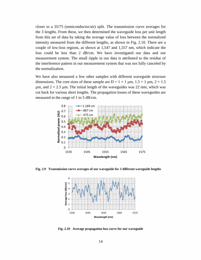
14
closer to a 35/75 (semiconductor/air) split. The transmission curve averages for
the 3 lengths. From these, we then determined the waveguide loss per unit length
from this set of data by taking the average value of loss between the normalized
intensity measured from the different lengths, as shown in Fig. 2.10. There are a
couple of low-loss regions, as shown at 1,547 and 1,557 nm, which indicate the
loss could be less than 2 dB/cm. We have investigated our data and our
measurement system. The small ripple in our data is attributed to the residue of
the interference pattern in our measurement system that was not fully canceled by
the normalization.
We have also measured a few other samples with different waveguide structure
dimensions. The core sizes of these sample are D = 1 × 1 µm, 1.5 × 1 µm, 2 × 1.5
µm, and 2 × 2.5 µm. The initial length of the waveguides was 22 mm, which was
cut back for various short lengths. The propagation losses of these waveguides are
measured in the range of 1 to 5 dB/cm.
Fig. 2.9 Transmission curve averages of our waveguide for 3 different waveguide lengths
Fig. 2.10 Average propagation loss curve for our waveguide
0
0.1
0.2
0.3
0.4
0.5
0.6
0.7
0.8
1535 1545 1555 1565 1575
No
rmal
ize
d p
ow
er
(AU
)
Wavelength (nm)
1.169 cm
.867 cm
.475 cm
0
1
2
3
4
5
6
1535 1545 1555 1565 1575
Ave
rage
loss
(d
b/c
m)
Wavelength (nm)
15
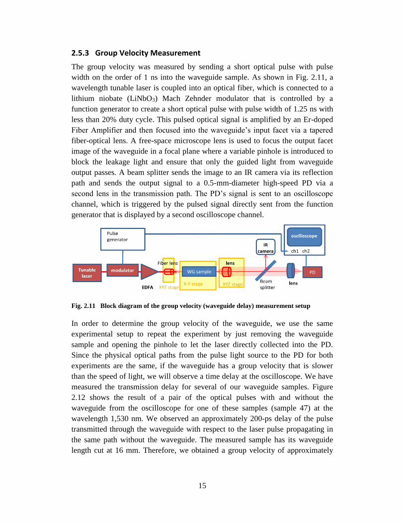
2.5.3 Group Velocity Measurement
The group velocity was measured by sending a short optical pulse with pulse
width on the order of 1 ns into the waveguide sample. As shown in Fig. 2.11, a
wavelength tunable laser is coupled into an optical fiber, which is connected to a
lithium niobate (LiNbO3) Mach Zehnder modulator that is controlled by a
function generator to create a short optical pulse with pulse width of 1.25 ns with
less than 20% duty cycle. This pulsed optical signal is amplified by an Er-doped
Fiber Amplifier and then focused into the waveguide’s input facet via a tapered
fiber-optical lens. A free-space microscope lens is used to focus the output facet
image of the waveguide in a focal plane where a variable pinhole is introduced to
block the leakage light and ensure that only the guided light from waveguide
output passes. A beam splitter sends the image to an IR camera via its reflection
path and sends the output signal to a 0.5-mm-diameter high-speed PD via a
second lens in the transmission path. The PD’s signal is sent to an oscilloscope
channel, which is triggered by the pulsed signal directly sent from the function
generator that is displayed by a second oscilloscope channel.
Fig. 2.11 Block diagram of the group velocity (waveguide delay) measurement setup
In order to determine the group velocity of the waveguide, we use the same
experimental setup to repeat the experiment by just removing the waveguide
sample and opening the pinhole to let the laser directly collected into the PD.
Since the physical optical paths from the pulse light source to the PD for both
experiments are the same, if the waveguide has a group velocity that is slower
than the speed of light, we will observe a time delay at the oscilloscope. We have
measured the transmission delay for several of our waveguide samples. Figure
2.12 shows the result of a pair of the optical pulses with and without the
waveguide from the oscilloscope for one of these samples (sample 47) at the
wavelength 1,530 nm. We observed an approximately 200-ps delay of the pulse
transmitted through the waveguide with respect to the laser pulse propagating in
the same path without the waveguide. The measured sample has its waveguide
length cut at 16 mm. Therefore, we obtained a group velocity of approximately

16
21% speed of light, C. This is the same sample for which we measured the
propagation loss, as shown in the last subsection of this report.
Fig. 2.12 Transmitted pulses from the oscilloscope with (blue) and without (red) the
waveguide. For comparison, reference pulse intensity is multiplied by a factor of 2 (green)
for normalization. Comparing the 2 pulse positions, there is a delay of about 200 ns of the
pulse passing through the waveguide.
We also plot the delay time of the peak position as a function of laser wavelength
from the waveguides in sample 47. Figure 2.13 shows these plots from one short-
arm support waveguide, one long-arm support single waveguide, and the
reference. We have measured other waveguide samples of different fabrication
batches with slightly different structure dimensions. Using the physical length of
these waveguide samples, we determined the group velocity of these waveguides
to be in the range of 20%–30% of the speed of the light.
Fig. 2.13 Plot of the pulse peak position as a function of time for a pulse transmitted from a
waveguide with short-arm support (blue), long-arm waveguide (green), and the reference
pulse (red)
-0.01
0
0.01
0.02
0.03
0.04
0.05
0 1 2 3 4
Pu
lse
In
ten
sity
(a.
u.)
Time (ns)
WG sample 47L=16mmλ=1530
WG#47
Ref
Ref(x2)
1.65
1.7
1.75
1.8
1.85
1.9
1525 1535 1545 1555 1565
tim
e (
ns)
Wavelength (nm)
WG47(short-arm)
Reference
WG47(long-arm)

17
2.6 Discussion
The challenge is to obtain both slow-light and low-loss properties in the same
operation bandwidth. The preliminary 2-D computation model indicates a
bandwidth of 100 GHz of group velocity of 0.02c slow-light region with a
0.1 dB/cm low-loss. Our experimental results seem to be much worse than that
model predicted. However, the preliminary modeling was made for a 2-D slab
waveguide configuration formed by 2 infinitely large ideal HCGs; therefore, the
results do not reflect our 3-D waveguide case. In the 3-D cage waveguide
configuration, there must be “corner effects”, and the polarization properties are
also different compared with the 2-D case. We are developing 3-D simulation
model codes to calculate the 3-D cage waveguide structure. Preliminary results do
indicate a higher loss. In addition, this discrepancy could be attributed to a
number of other factors:
Fabrication error: From the SEM pictures, we can see that some of these
samples still have the needle bars in the middle of the core region, and
there is scalloping roughness on the vertical walls/posts, as well as a
curved bottom grating shape.
Measurement error: Since the insertion/coupling losses are an order of
magnitude higher than the propagation loss, it is very difficult to repeat the
exact coupling condition for each cleaves from sample to sample. There is
also interference in our measurement system and unstable laser tuning that
can increase the error in our measurement.
Wavelength: We have a limited tuning range and tuning step accuracy for
our laser. The wavelength or size discrepancy can occur between the
calculated model and the real sample, which can put us outside of the
optimum spot. Therefore, it is no surprise that we have not seen the
desired slow-light/low-loss region from our first preliminary experiment.
Either our laser tuning range could not reach the right wavelength or the
fabrication errors are preventing the slow-light/low-loss region from being
formed.
The preliminary calculation suggested that increasing the hollow core size D may
reduce the propagation loss. However, reducing the hollow core size may reduce
the group velocity. We aim to develop a better 3-D simulation model to calculate
the exact 3-D cage waveguide structures in order to guide us in finding the
optimum slow-light and low-loss spot. In the meantime, we are currently
improving our fabrication tolerance/uniformity, fabricating and testing a large
number of samples with slight variations in the metastructure period, duty cycle,

18
core size, grating width, etc., in order to reach a better slow-light/low-loss region
experimentally.
2.7 Conclusion
We have demonstrated a new type of Si-based, high-contrast metastructure with a
cage-like hollow-core waveguide that has both slow-light and low-loss properties.
These 3-D metastructure cage waveguides were fabricated on an SOI wafer using
our new nanofabrication techniques with the self-aligned modified Bosch etching
process and modified SCREAM etching process. We experimentally
demonstrated a group velocity of 0.2c slow-light waveguide propagation with
about –2 dB/cm propagation loss. We continue to improve our fabrication process
and our simulation model to reduce the loss and group velocity. This type of
slow-light metawaveguide can provide a long time delay and high Q cavity in Si-
based OEIC for chip-scale integrated photonics, RF-photonics, and systems for
communication, radar, computation and sensor applications.

19
2.8 References
1. Mateus C, Huang M, Yunfei D, Neureuther A, Chang-Hasnain C. Ultra
broadband mirror using low-index cladded subwavelength grating. IEEE
Photonic Technology Let. February 2004;16(2):518–520.
2. Chang-Hasnain C. Zhou Y, Huang M, Chase C. High-contrast grating
VCSELs. IEEE J Sel Top Quantum Electron. 2009;15(3):869–878, and
Huang et al. A surface-emitting laser incorporating a high-index-contrast
subwavelength grating. Nature Photonics. 2007;1:119.
3. Zhou Y, et al. Ultra-low loss hollow-core waveguides using high-contrast
gratings. In: Proceedings of the Conference on Lasers and Electro-
Optics/International Quantum Electronics Conference, 2009.
4. Zhou W, et al. Slow light high contrast metastructure hollow-core
waveguides. Proc SPIE. 2012;8270:827009-1.
5. Sun T, et al. Low-loss slow light inside high contrast grating waveguide. Proc
SPIE. 2012;8270:82700A-1.
6. Zhou W. Semiconductor hollow-core waveguide using photonic crystal
gratings. United States patent US 8,506,829. 2013 Aug 13.
7. Laermer F, Schilp A. Method of anisotropically etching silicon. United States
patent US 5,501,893. 1996 Mar 26.
8. Shaw KA, et al. SCREAM I: a single mask, single-crystal silicon process for
microelectromechanical structures. In: MEMS ’93. Proceedings of 1993
IEEE Micro Electro Mechanical Systems: An Investigation of Micro
Structures, Sensors, Actuators, Machines and Systems; 1993 Feb 7–10; Fort
Lauderdale, FL. New York (NY): IEEE. 1993; p. 155–160.
9. Soukoulis CM. The history and a review of the modeling and fabrication of
photonic crystals. Nanotechnology 2002;13:420–423.
10. Taysing-Lara M, Dang G, Zhou W. A new fabrication method for 3D Si-
based photonic crystal structure. Proc. of SPIE. 2011;7927:792707-1.

20
3. Design and Fabrication of 3-dimensional (3-D) High-Contrast Metastructure Terahertz Cage Waveguides
Gerard Dang, Monica Taysing-Lara, Weimin Zhou (SEDD)
3.1 Abstract
We have designed a new terahertz metastructure waveguide on Si wafers, aimed
for low propagation loss and integration with Si-based integrated circuits (ICs).
The waveguide has a round cross-section hollow core surrounded by a high-
reflecting cladding wall, which is made by high-contrast metastructure gratings.
We developed a new fabrication technique to fabric such a 3-dimensional (3-D)
metastructure cage-like waveguide structure. The waveguide is built with an
entire wafer thickness, which involves a deep silicon (Si) etch of periodically
spaced holes and isotropic undercut etching to create a connecting circular hole in
the middle of the wafer to form the waveguide’s hollow core, then deep etch the
high-contrast grating (HCG) through the whole wafer to form the cladding for the
waveguide. We have successfully fabricated such a waveguide structure. The next
step is to experimentally test and characterize the waveguide in the terahertz
spectrum range.
3.2 Introduction
In recent years, there has been growing interest in terahertz research because of
attractive applications, such as see-through imaging, chemical/biosensing and
line-of-sight communications. However, terahertz technology is still in its
infancy. Other than a few traditional optics, there is a lack of necessary devices
and components to build circuitry to manipulate terahertz signals. To develop
terahertz devices and components, the basic element is a terahertz waveguide.
Using the traditional metal-tube microwave waveguide technology to build
terahertz waveguides will result in high loss and high cost; plus, this traditional
technology cannot be integrated with Si-based ICs.
Previously, we have developed a new type of 3-D cage-like high-contrast
metastructure hollow-core waveguide that showed reasonable low-loss and slow-
light effect at 1,550-nm operation wavelength.1-3 It has been demonstrated that the
high-contrast metastructure grating can be designed for very high reflectivity.1 It
then can be incorporated as the reflector in a hollow core waveguide without the
use of metal. One of the potential applications for such a waveguide is in
chemical gas sensing, because the cage design provides an open form of a high-Q
21
cavity that can be integrated with a light source and detector. However, it is
desirable to perform the chemical sensing in the terahertz regime that has a less
busy spectrum for easy chemical identification. Therefore, we have used the same
design concepts to change the wavelength scale from infrared to terahertz to
design a low-loss terahertz waveguide. We have developed a new fabrication
technique to fabricate a terahertz metastructure cage waveguide on Si wafers.
3.3 Waveguide and Fabrication Designs
3.3.1 Waveguide Design and Simulation
Figure 3.1 illustrates a targeted cage-like high-contrast metastructure hollow-core
terahertz waveguide structure to be constructed in an Si wafer. Since the
electromagnetic wave at terahertz is in the order of 100 s µm in wavelength, we
have to use the entire Si wafer thickness (~550 µm) to construct the waveguide.
First, we worked with our collaborator at UC Berkeley to develop a theoretical
computational model to simulate such a waveguide structure in order to guide us
to design the hollow-core waveguide using the high-contrast metastructure
gratings as waveguide cladding.
Fig. 3.1 Two- and three-dimensional cross-sectional diagrams of the terahertz hollow-core
waveguide with high-contrast gratings. The axis for waveguiding is into the center of the
cylindrical hollow core.
3.3.1.1. Dispersion Relation and Mode Pattern
To study the dispersion relation (i.e., ω𝜔-β𝛽 diagram) of our 3-D waveguide, we
use the dipole excitation method. In this method, dipoles with random orientation
are put into the waveguide hollow core. Bloch boundary condition is set at 2
facets of one period. These dipoles will excite many modes inside the hollow
core. After a long time decaying, only the intrinsic waveguide modes will build
up a strong field and are shown to have strong field strength (shown as red color
in Fig. 3.2a), and other lossy modes will decay out, leaving little intensity (shown

22
as white color in Fig. 3.2a). In this way we can study the dispersion relation inside
our novel waveguide.
We simulated the dispersion relation for a waveguide with 2- × 2-µm core size,
grating period 1 µm, duty cycle approximately 0.5, thickness for top/bottom
grating 0.71 µm, and thickness for 2-side grating 1.77 µm. Dipoles excited modes
with different frequencies and different wave vectors. When a stable state is
reached, only the intrinsic mode will build up; this is shown as the red color in
Fig. 3.2a. The black dashed line highlights the deep red region and indicates the
mode dispersion curve. This mode is the intrinsic low loss mode supported by the
structure. The black solid curve is the light line shown as general guidance. This
particular waveguide supports the fundamental mode operation in the wavelength
region we are interested in. The mode pattern for this fundamental mode is shown
in Fig. 3.2b at a frequency of 1.698 THz, which is in the center of the fundamental
mode band shown in Fig. 3.2a.
Fig. 3.2 a) Dispersion relation diagram of our 3-D waveguide. b) Mode pattern of the fundamental
mode in our 3-D waveguide.
3.3.1.2. Intrinsic Propagation Loss
In this subsection, we will estimate the intrinsic loss of our hollow-core
waveguide. An optical pulse centered at 1.698 THz with a 10-ps pulse is sent into
the waveguide. The excitation and subsequent decay of the waveguide mode is
sampled at various points inside the waveguide. The associated amplitude time
signal is plotted in Fig. 3.3. We can see the source pulse at the very beginning and
the slow decay of the intrinsic mode. Loss is then estimated following the formula
loss (dB
m) = 10 × log10 𝑒 × 𝑠/𝑣𝑔

23
where s is the slope of the decaying , and vg is the group velocity of the mode. For
the mode shown in Fig. 3.3, s is around 2 × 10⁷/s and vg is around 107 m/s. Thus,
the estimated the intrinsic loss is around 8.6 dB/m. This loss can be further
brought down by designing more reflective HCG as the waveguide walls.
Fig. 3.3 The excitation of a 10-ps pulse and subsequent decay of the waveguide mode. Slope
of the decaying is proportional to the waveguide loss.
3.3.2 Fabrication Technique
Unlike the near-IR hollow-core waveguides with HCGs we previously fabricated,
e-beam lithography is not needed to fabricate these waveguides. The features are
on the scale of tens of microns, and standard photolithography can be used. But,
because of the large size of the waveguide core, we cannot use the same undercut
etching method that we previously used for the near-IR hollow-core waveguide
fabrication. To fabricate these terahertz waveguides, we need to develop a new
undercut etch technique to create the 3-D cage-like structure that uses
approximately 500 µm (entire wafer thickness) to construct the waveguide. As
shown in Fig. 3.1, the waveguide core size is approximately 150 µm, leaving
cladding dimensions of 175 µm. We used a modified “SCREAM” (Single-Crystal
silicon REactive etch and Metal) process,4 such as using a masking oxide on the
surface of the wafer as well as on the sidewalls of etched trenches, but we also use
chromium metal in addition to an oxide. We modified the process by using an
inductively coupled plasma etching system, instead of a Reactive Ion Etcher, for
our deep silicon etches. Also, instead of deposition of the oxide, we used wet
thermo-oxidization of the Si to create the making layer.
We designed 2 photomask levels with grating patterns with a period of 100 µm
and an approximately 50/50 duty cycle. As shown in Fig. 3.4, the first level of the
mask design is used to access the center of the wafer to form the hollow core by

24
using a modified SCREAM process to undercut etch a column of connecting
spherical holes to ultimately form a cylindrical hollow core for the waveguide.
The second level is used to complete the formation of the high-contrast
metastructure cladding in the waveguide via a deep Si etch through the entire
thickness of the wafer.
Fig. 3.4 Truncated .gds layout of overlaid mask levels. This would translate to a top view of
the fabricated waveguide. The small boxes between the waveguides are alignment marks.
3.4 Fabrication
3.4.1 Undercutting Etch to Form the Waveguide Hollow Core
We are performing long-duration dry etches to form the features of the
waveguide, so masking is important in the fabrication process. We start by
growing a silicon dioxide (SiO2) layer on the wafer using a wet thermo-oxidation
furnace. The SiO2 will be used as one way to protect the surface of the wafer
during etching. The target thickness of the SiO2 is 3 µm. Using AZ9260
photoresist spun-on and baked for a final photoresist thickness of 9 µm, we
expose the photoresist with a pattern of the proper dimension for forming the core
of the waveguide. The dark-colored rectangular boxes in Fig. 3.2 show the pattern
used for this part of the process. These features after processing are about 50 ×
200 µm in the Si. This mask level is used to etch down a series of deep trenches
25
about the height of the top grating (175 µm) to reach the top of the core area of
the waveguide. These deep trenches provide access to the center of the wafer for
the isotropic undercut etch for formation of a cylindrical core of the waveguide.
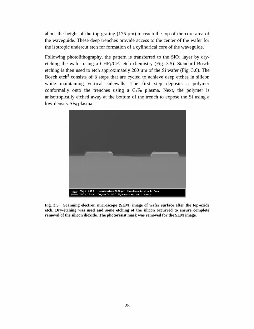
Following photolithography, the pattern is transferred to the SiO2 layer by dry-
etching the wafer using a CHF3/CF4 etch chemistry (Fig. 3.5). Standard Bosch
etching is then used to etch approximately 200 µm of the Si wafer (Fig. 3.6). The
Bosch etch5 consists of 3 steps that are cycled to achieve deep etches in silicon
while maintaining vertical sidewalls. The first step deposits a polymer
conformally onto the trenches using a C4F8 plasma. Next, the polymer is
anisotropically etched away at the bottom of the trench to expose the Si using a
low-density SF6 plasma.
Fig. 3.5 Scanning electron microscope (SEM) image of wafer surface after the top-oxide
etch. Dry-etching was used and some etching of the silicon occurred to ensure complete
removal of the silicon dioxide. The photoresist mask was removed for the SEM image.
26
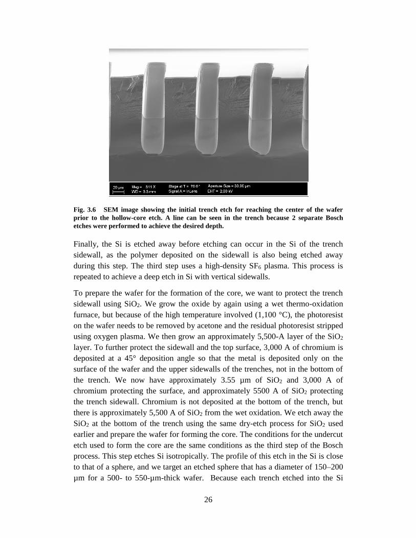
Fig. 3.6 SEM image showing the initial trench etch for reaching the center of the wafer
prior to the hollow-core etch. A line can be seen in the trench because 2 separate Bosch
etches were performed to achieve the desired depth.
Finally, the Si is etched away before etching can occur in the Si of the trench
sidewall, as the polymer deposited on the sidewall is also being etched away
during this step. The third step uses a high-density SF6 plasma. This process is
repeated to achieve a deep etch in Si with vertical sidewalls.
To prepare the wafer for the formation of the core, we want to protect the trench
sidewall using SiO2. We grow the oxide by again using a wet thermo-oxidation
furnace, but because of the high temperature involved (1,100 °C), the photoresist
on the wafer needs to be removed by acetone and the residual photoresist stripped
using oxygen plasma. We then grow an approximately 5,500-A layer of the SiO2
layer. To further protect the sidewall and the top surface, 3,000 A of chromium is
deposited at a 45° deposition angle so that the metal is deposited only on the
surface of the wafer and the upper sidewalls of the trenches, not in the bottom of
the trench. We now have approximately 3.55 µm of SiO2 and 3,000 A of
chromium protecting the surface, and approximately 5500 A of SiO2 protecting
the trench sidewall. Chromium is not deposited at the bottom of the trench, but
there is approximately 5,500 A of SiO2 from the wet oxidation. We etch away the
SiO2 at the bottom of the trench using the same dry-etch process for SiO2 used
earlier and prepare the wafer for forming the core. The conditions for the undercut
etch used to form the core are the same conditions as the third step of the Bosch
process. This step etches Si isotropically. The profile of this etch in the Si is close
to that of a sphere, and we target an etched sphere that has a diameter of 150–200
µm for a 500- to 550-µm-thick wafer. Because each trench etched into the Si

27
wafer is 50 µm away from an adjacent trench, the etched sphere punches through
to form a cylindrical core along the length of the waveguide. Figure 3.7 shows a
scanning electron microscope (SEM) image of the hollow-core etch. The surface
of the sample used for this image shows damage from the scribe because a
continuous cleaving plane in this direction does not exist in the Si after the hollow
core is formed. So the waveguide’s core is formed by the connecting spheres in
the center of the Si wafer.
Fig. 3.7 SEM image showing the hollow-core etch in the wafer and the etched spheres
punching through to adjacent spheres. The surface of the sample used for this image shows
damage from the scribe because a continuous cleaving plane does not exist after the hollow
core is formed.
3.4.2 Deep Through-Wafer Etch to Form the Waveguide’s High-Contrast-Grating (HCG) Metastructure Cladding
Following the formation of the core, photolithography is performed again using a
longer-lines feature to form the HCGs as the cladding of the waveguide. These are
the longer grating features shown in the mask pattern in Fig. 3.4 that overlay the
smaller rectangular features that were used for the under-cut etching of the core in
the center of the waveguide. The dimensions of these grating bar features after
processing are 50 µm × 1 mm. In order to etch into the Si using the wider grating
feature, we must first etch through the chromium that was deposited earlier and
the SiO2 layer. The chromium is wet-etched using CR-9, which selectively etches

28
away the metal and not the SiO2. The SiO2 is then dry-etched using the same
process as earlier. We then perform a Bosch etch through the entire thickness of
the wafer to define the HCG claddings of the waveguide. Figure 3.8 shows a SEM
image of the waveguide processed up to this point, viewing it in the direction of
waveguiding.
Fig. 3.8 Cross-sectional SEM images of the waveguides. (Top) An SiO2 shell in the shape of
the first trench etched can be seen at the top of the hollow core. (Bottom) The SiO2 shell in
the core was removed by buffered high-frequency etch.
The bottom corner of this facet is rough in the image because of scribing for
preparing the SEM sample, but the bottom surface of the wafer is polished Si. The
top SEM picture shows a shell of SiO2 in the core of the waveguide. This was
formed by wet oxidation in the trench sidewalls of the smaller grating feature
used to access the center of the wafer prior to the hollow-core etch. The shell
remains, as the Bosch process is highly selective to etching Si over SiO2. We

29
remove any remaining SiO2 on the waveguides by etching the wafer in buffered
oxide etch as shown in the lower SEM picture. Figure 3.9 shows 2 SEM images
of the completed waveguide.
Fig. 3.9 SEM images of the waveguides after etching in CR-9 and buffered oxide etchant
3.5 Conclusion
We have designed and fabricated new terahertz high-contrast metastructure cage
hollow-core waveguides. These 3-D metastructure cage waveguides were
fabricated on standard 4-inch Si wafers with a thickness of approximately 550 µm
using modified SCREAM and Bosch etch processes. We are continuing to
improve our fabrication process and are preparing the waveguides for testing and
measuring propagation loss. This type of waveguide can potentially be used as a
basic building component in circuitry designed to manipulate terahertz signals as
well as a chemical-biological sensor because of its open-cage design.

30
3.6 References
1. Zhou Y, et al. Ultra-low loss hollow-core waveguides using high-contrast
gratings. In: Proceedings of the Conference on Lasers and Electro-
Optics/International Quantum Electronics Conference, 2009.
2. Zhou W. Semiconductor hollow-core waveguide using photonic crystal
gratings. United States patent US 8,506,829. 2013 Aug 13.
3. Zhou W, Dang G, Taysing-Lara M. Demonstration of a slow-light high-
contrast metastructure cage waveguide. Proc. of SPIE Vol. 8633; High
Contrast Metastructures II; 2013 Mar 15. 863305.
4. Shaw KA, et al. SCREAM I: a single mask, single-crystal silicon process for
microelectromechanical structures. In: MEMS ’93. Proceedings of 1993
IEEE Micro Electro Mechanical Systems: An Investigation of Micro
Structures, Sensors, Actuators, Machines and Systems; 1993 Feb 7–10; Fort
Lauderdale, FL. New York (NY): IEEE. 1993; p. 155–160.
5. Laermer F, Schilp A. Method of anisotropically etching silicon. US Patent
No. 5501 893.
31
4. Tunable Terahertz Metamaterial Devices
Monica Taysing-Lara, Gerard Dang, Grace Metcalfe, Nathaniel Woodward,
Weimin Zhou (EO&P, SEDD)
Daniel Shreiber, Eric Ngo, Matt Ivill, Melanie Cole (M&MS, WMRD)
Amir Zaghloul (E&RF, SEDD)
4.1 Abstract
We have designed several tunable terahertz metamaterial structures containing 3-
dimensional (3-D) metal split-rings with a tunable capacitor fabricated using
complex oxide thin films (in this case, BaSrTiO3 [BST]). Subsequently, the team
developed a new fabrication technique and successfully fabricated such a 3-D
tunable metamaterial device. In addition, a simulation model was developed to
assist the metamaterial device design and predict the resonance frequency and
tuning. The model has also been used to determine the dielectric constant of the
BST thin film and to assist in BST thin film tunability measurements. This is, to
our knowledge, the first effort to measure the BST thin film tunability in the
terahertz spectrum.
The free space evaluation of the metamaterial device in the terahertz spectrum has
been performed and is in general agreement with the stated goals of this DSI: a
fabrication of a tunable metamaterial device in the terahertz spectrum.
4.2 Introduction
Metamaterial is a man-made material that has some engineering-designed
electromagnetic properties, such as specific ε and µ in a desired frequency
bandwidth. In order to obtain a desired value for ε and µ (in particular, the
negative values for ɛ and μ are of special interest), one has to manipulate or create
certain energy state “transitions”. That can be done by creating a group of micro-
resonators as unit cells in the metamaterial, such as metal split-ring resonators. In
this project, our objective is to develop a tunable metamaterial device in the
terahertz operation band. There are many interesting terahertz system applications
for the Army, such as see-through imaging, chemical/biosensing, and line-of-sight
communications. However, terahertz technology is still in its infancy. There is a
lack of necessary devices and components to build circuitry to manipulate
terahertz signals. To develop terahertz devices and components, the traditional
materials often have inadequate electromagnetic properties that result in loss or
unresponsiveness if used to build a terahertz device. Metamaterial may offer new

32
opportunities for solving this problem, and tunable metamaterial may provide
even more freedom for design of such a terahertz device. The most desirable
electromagnetic property for such a metamaterial is to have the value of ε and µ to
be able to tune over a certain terahertz frequency range, to have a tunable
resonance, or have the so-called double negative ε and µ so that special optical
properties can be realized. However, this will require a special 3-D geometric
topology for the split-ring unit cells; the traditional semiconductor device
fabrication processing technique may not be able to realize such device geometry.
In this project, we developed a new fabrication technique which allows us to build
a specific 3-D split-ring structure that realizes the desired device’s geometric
configuration. The goal of this project was to achieve the first step: to fabricate a
single negative tunable terahertz metamaterial device into a configuration that will
enable easy transformation into a double-negative device.
4.3 Design, Modeling, and Simulation
The DSI team worked together to design 8 versions of the tunable terahertz
metamaterials. Two of them that contain 3-D metal split-rings with tunable
capacitance fabricated using complex oxide (BST) thin films were down-selected.
Figure 4.1a shows the unit cell of the metamaterial device. A tunable capacitor is
formed in the gap of the metal split-ring. A complex oxide (BST) thin film is used
as the dielectric media for the capacitor because BST has a very high dielectric
constant in the high-frequency band. The BST thin film on top of a substrate
(sapphire) is sandwiched between 2 metal electric strip lines that are
perpendicular to the surface of the split-ring. A direct-current (DC) bias can be
applied to these electrodes to tune the capacitance in between the metal split-ring.
The standing-up metal split-ring is wrapped around on the surface of a rectangular
polymide ridge bar, which is formed on top of the substrate and BST film. Figure
4.1b shows the split-ring arrays with the DC metal bias electrodes that can apply
bias to all the capacitors in the gaps of the split-rings.
The Weapons and Materials Research Directorate (WMRD) team led the
simulation work of the metamaterial and the thin-film growth development of the
Ba1-xSrxTiO3 (BST) as the tunable capacitor material. A commercially available
high-frequency structural simulator (HFSS) software that solves Maxwell
equations for the waves propagating in the materials of interest has been used to
develop the model for the simulation. Figure 4.2 shows simulation results,
indicating that in addition to the resonant peak, interesting effects of nonresonant
energy dissipation of the impinging wave at certain frequencies can be seen as a
result of the interference-like behavior.

33
Fig. 4.1a Tunable 3-D terahertz metamaterial unit cell. (Left) Cross section of the split-ring
unit cell with complex oxide film as tunable capacitor (right) and (right inset) scanning
electron microscopy (SEM) picture.
Fig. 4.1b 3-D illustration of the tunable metamaterial
Fig. 4.2 HFSS model simulation of the test surfaces showing the resonant frequency and
some nonresonant energy dissipation

34
In the Sensors and Electron Devices Directorate (SEDD), we developed a method
of measuring and analyzing the complex refractive index of a variety of thin
films, as well as substrate material, using differential time-domain terahertz
spectroscopy (TDTS) in the 0.1- to 2-THz range (Fig. 4.3).
Fig. 4.3 (Left) Time-resolved terahertz transmission spectroscopy data and (right) complex
refractive index of a polyimide thin film on sapphire
The experimentally measured indices are used in the simulation model, which
predicts the resonant frequency of the metamaterial. For example, a shift of 0.11
THz occurred when the dielectric constant of the BST was increased from 100 to
500. Using the differential TDTS system, we measured the refractive index of the
substrate material’s sapphire as n = 3.06 ± i0.01 and silicon as n = 3.52 ± i0.02 in
the terahertz frequency range. For thin films, we measured n = 2.25 ± i0.04 for a
9.54-µm-thick polymide film on a sapphire substrate. As seen in Fig. 4.1, the
polymide is part of the 3-D metamaterial structure.
The model has been devised to predict the resonance response of the designed
metamaterial surface when the dielectric constant of the BST thin film is known
or, alternatively, the model can determine the dielectric constant of the BST film
by comparison with the experimental data (Fig. 4.4).
-2 -1 0 1 2 3 4 5 6 7 8 9 10-6
-4
-2
0
2
4
6
TH
z a
mplit
ude (
arb
. u.)
Time delay (ps)
incident THz field
substrate only
substrate and polyimide
0.2 0.4 0.6 0.8 1.0 1.2 1.4 1.6 1.8 2.0 2.2
0.0
0.5
1.0
1.5
2.0
2.5
Re(n)
Im(n)n
Frequency (THz)

35
-30
-25
-20
-15
-10
-5
0
0.2 0.4 0.6 0.8 1 1.2 1.4 1.6
S21
S21
f(THz)
Fig. 4.4 Results from the HFSS model of the designed and implemented metamaterial
surface. The location of the resonance peak is accurately predicted with assumed value of
BST dielectric constant.
Hence, the model can be applied to find the change in dielectric constant from the
resonance peak shift when the DC voltage bias is applied. Figure 4.5 shows the
simulated resonance shift of 1 GHz when the dielectric constant of BST is
increased from 170 to 180. This is the first time the tunability of BST in the
terahertz regime has been measured as a function of bias in the metamaterial
device. The experimental results of the resonant frequency shift by 2 GHz (when
6 V is applied) were compared with the confirmed model that showed a 1-GHz
leftward shift of the resonant frequency peak when the dielectric constant of BST
is increased from 170 to 180.

36
Fig. 4.5 HFSS model of the metamaterial device when BST thin film is assumed to have a
dielectric constant of 170 (blue) and 180 (red). The 1-GHz leftward shift is analogues to the
4-V bias applied to the device (experimental data).
4.4 Fabrication
4.4.1 Develop Fabrication Technique
Led by SEDD, we developed a new fabrication technique for the tunable split ring
resonators. The fabrication consists of a bottom bias electrode metal on a sapphire
substrate, the BST layer, a top bias electrode metal, and a 5,000-Å copper
deposition for the bottom of the split-ring. Then a 10-μm polyimide rib structure
is built.
4.4.2 BST Thin Film Growth
A 180-nm-thick BST film was grown and characterized both at SEDD and
WMRD. The thin film was grown at an ambient temperature of 490 °C, base
pressure of 5 × 10^–8 Torr, and deposition pressure of 10 mTorr. The deposition
gas mixture was 90%Ar/10% O2. The deposition time was 4 h 15 min at radio
frequency (RF) power of 150 W. Figure 4.6 shows one of the BST thin films
grown at WMRD. Although the BST film was too thin to measure the complex
refractive index accurately, the refractive index can still be deduced by measuring
the metamaterial resonance frequency with the help of the devised model.
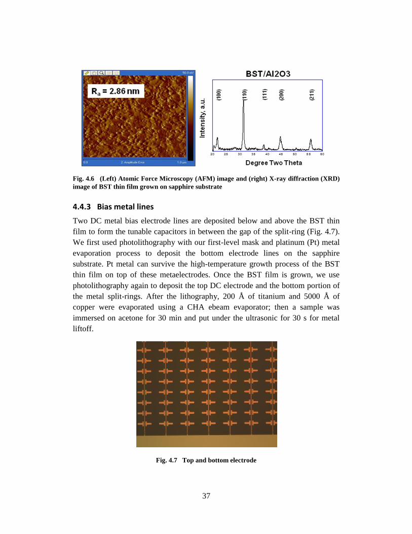
37
Fig. 4.6 (Left) Atomic Force Microscopy (AFM) image and (right) X-ray diffraction (XRD)
image of BST thin film grown on sapphire substrate
4.4.3 Bias metal lines
Two DC metal bias electrode lines are deposited below and above the BST thin
film to form the tunable capacitors in between the gap of the split-ring (Fig. 4.7).
We first used photolithography with our first-level mask and platinum (Pt) metal
evaporation process to deposit the bottom electrode lines on the sapphire
substrate. Pt metal can survive the high-temperature growth process of the BST
thin film on top of these metaelectrodes. Once the BST film is grown, we use
photolithography again to deposit the top DC electrode and the bottom portion of
the metal split-rings. After the lithography, 200 Å of titanium and 5000 Å of
copper were evaporated using a CHA ebeam evaporator; then a sample was
immersed on acetone for 30 min and put under the ultrasonic for 30 s for metal
liftoff.
Fig. 4.7 Top and bottom electrode

38
4.4.4 3-D Split-Ring Fabrication
To create the standing metal split-rings, we need to first form an array of
polyimide rectangle ridge bars that have a cross-section size that matched the
split-ring size, which is about 10 µm high and 50 µm wide. The center of these
ridge bars was aligned on top of the bottom portion of the split-ring that is already
deposited on the substrate with the tunable capacitors that were made in previous
steps. A third-level mask is used to create these polyimide bars by lithography and
high-temperature curing as follows: Polyimide HD 4100 was poured using a
dropper and let sit for 5 min; air bubbles at the top were removed with the
dropper. Then the sample was spun at 1,500 rpm for 40 s and soft-baked at
furnace for 10 min at 95 °C. Poly Mask was used to expose the polyimide for 15 s
using 300 W and post-expose-baked at the furnace at 95 °C for 50 s. The
polyimide was developed by immersing the sample on the PA 401 solution for 2
min and rinsing on the PA 400 solution for 30 s; after that, it was blow-dried with
the air gun. Finally, the sample was hard-baked at the furnace under oxygen, and
the temperature was increased at a rate of 10 °C/min until 200 °C then baked for
30 min, then increased at the same rate to a temperature of 375 °C and baked for
60 min. The polyimide scum from the top of the metal was removed by using the
Metroline/IC Plasma using 200 sccm of oxygen and the power of 200 mW at the
pressure of 1 Torr for 10 min. The polyimide thickness, 9.8 µm, was obtained
using a SEM.
Once the polyimide bars are made, we spin a thick photoresist on top of it. Using
the fourth-level mask lithography, we open a line slot on the photoresist that is
across the top of the polyimide bar so that a series of lines on the top and side of
the polyimide are exposed. The next step is to evaporate metal by tilting and
rotating the wafer 45° to the evaporation source. Then, 200 Å of titanium and
5,000 Å of copper were deposited using a CVC 610 sputtering system. The
sample was immersed in acetone for 30 min and put under the ultrasonic for 30 s
for metal liftoff. The result is that a series of half metal rings are wrapped around
the polyimide bars. The first fabricated metamaterial device is shown in Fig. 4.8.
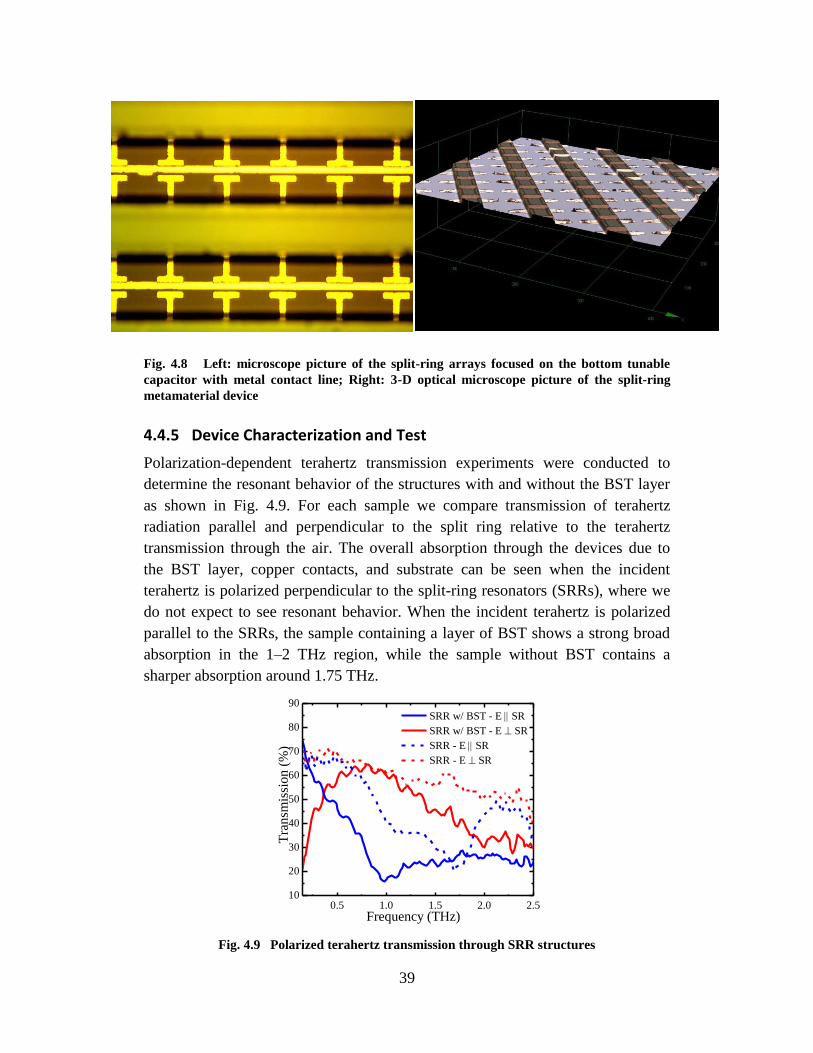
39
Fig. 4.8 Left: microscope picture of the split-ring arrays focused on the bottom tunable
capacitor with metal contact line; Right: 3-D optical microscope picture of the split-ring
metamaterial device
4.4.5 Device Characterization and Test
Polarization-dependent terahertz transmission experiments were conducted to
determine the resonant behavior of the structures with and without the BST layer
as shown in Fig. 4.9. For each sample we compare transmission of terahertz
radiation parallel and perpendicular to the split ring relative to the terahertz
transmission through the air. The overall absorption through the devices due to
the BST layer, copper contacts, and substrate can be seen when the incident
terahertz is polarized perpendicular to the split-ring resonators (SRRs), where we
do not expect to see resonant behavior. When the incident terahertz is polarized
parallel to the SRRs, the sample containing a layer of BST shows a strong broad
absorption in the 1–2 THz region, while the sample without BST contains a
sharper absorption around 1.75 THz.
0.5 1.0 1.5 2.0 2.510
20
30
40
50
60
70
80
90
Tra
nsm
issi
on
(%
)
Frequency (THz)
SRR w/ BST - E SR
SRR w/ BST - E SR
SRR - E SR
SRR - E SR
Fig. 4.9 Polarized terahertz transmission through SRR structures

40
We have characterized the first designed and fabricated active metamaterial with
time domain terahertz spectrometer (Figs. 4.10 and 4.11) for tunability.
Fig. 4.10 Schematics of the experimental setup for WMRD’s terahertz time-domain
spectrometer

41
Fig. 4.11 Resonant peak shift when the bias of 0, 2, and 6 V is applied to active
metamaterial in time-domain terahertz spectrometer. The inset shows a 2-GHz shift in
resonance frequency when a 6-V bias is applied.
Bias applied to the BST thin film (up to 6 V) had shifted the resonant peak of the
device by 2 GHz (from 1.142 to 1.14 THz) as indicated in the inset of Fig. 4.11.
The shift is quite remarkable since because of an insufficient thickness of the
bottom bias electrode, only a small portion of the “capacitor gap” is filled with
BST thin film (Fig. 4.12) and, hence, the fields that interact with the BST film are
much lower than the theoretical capability of the device.

42
Fig. 4.12 SEM of THz metamaterial unit cell with unfilled “capacitor gap”. The schematics
of the structure are provided in Fig. 4.1.
4.6 Terahertz Transparent Electrode Study
The efficiency of the metamaterial device can be further enhanced by using DC
bias electrodes composed of a DC conductor that is transparent to terahertz
radiation, e.g., indium tin oxide (ITO). ITO films were grown with varied ambient
argon (Ar)/oxygen (O2) ratios at WMRD and characterized at SEDD for
transparency in the terahertz regime (Fig. 4.13). We found the correct ratios to
produce the terahertz transparent ITO films with 2 orders of magnitude higher
resistivity with respect to the nontransparent ITO. The terahertz transparent
electrodes grown under the devised conditions can be used in future terahertz
metamaterial devices to enhance their efficiency.
Fig. 4.13 Transmission terahertz spectroscopy of ITO
43
4.7 Conclusion
The overarching goal of this part of the DSI—namely, demonstration of a tunable
metamaterial surface in the terahertz spectrum of radiation—has been achieved.
This tunable metamaterial surface will enable the design and fabrication of active
metamaterial devices in the terahertz spectrum. The architecture of the
metamaterial surface designed by the team allows for easy transformation from a
single negative to a double negative device. A numerical model has been devised
to match the experimental data and determine the dielectric constant of BST.
Alternatively, this model can be used to determine the resonant frequency of the
device in the terahertz spectrum. In addition, an investigation of the resonant peak
shift when the DC bias is applied with the model, and matching this shift with the
one obtained from experimental measurements, yielded the first measurement of
BST thin film tunability in the terahertz spectrum up to the bias of 6 V.
Experimental investigation of the designed metamaterial device also showed
polarization dependence of terahertz transmission through the device.
44
5. Radio Frequency Metamaterial Research
A Zaghloul, T Anthony, and SJ Weiss (E&RF, SEDD)
RF metamaterial research is focused on characterizing metamaterial properties at
frequency bands of interest to Army applications. Although the characterization
analysis is scalable in frequency, the work is mainly presented at the Ku-band.
For most of the analysis and measurements, the metamaterial structure is based on
the unit cell of capacitively loaded loop (CLL). This cell has been shown to
produce negative permeability in part of the frequency band. When combined
with a probe or wire, which is known to produce negative permittivity in part of
the band, a negative refractive index results in the medium. The cells are arranged
in periodic or random patterns, and each has certain properties that are studied.
An insight into the mechanism of the negative refraction provides a physical
explanation of this property under certain conditions in the wave propagation in
the material. The work discussed in this section has been reported in a number of
conference papers and presentations,1–9 an invention disclosure application
(pending),10 technical notes,11–13 and a master’s thesis14. References to these
publications are made, as appropriate, in the following subsections.
5.1 Capacitively Loaded Loop/Probe (CLL-P) Cell
Metamaterial cells that consist of metalized CLLs printed on dielectric substrate
constitute the main design used in this work. CLL is similar in function to the
split-ring resonator (SRR), as it operates on the permeability of the material
through coupling to the magnetic field. It was widely used in the literature to
realize negative permeability. The basic cell is shown in Fig. 5.1a. A metallic wire
or probe, on the other hand, oriented in parallel to the electric field operates on the
permittivity of the material and was used to realize negative permittivity at narrow
frequency bands. The combination of the CLL and the probe, called CLL-P, is
shown in Fig. 5.1b.
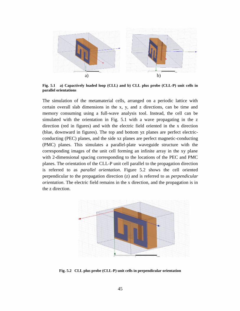
45
a) b)
Fig. 5.1 a) Capactively loaded loop (CLL) and b) CLL plus probe (CLL-P) unit cells in
parallel orientations
The simulation of the metamaterial cells, arranged on a periodic lattice with
certain overall slab dimensions in the x, y, and z directions, can be time and
memory consuming using a full-wave analysis tool. Instead, the cell can be
simulated with the orientation in Fig. 5.1 with a wave propagating in the z
direction (red in figures) and with the electric field oriented in the x direction
(blue, downward in figures). The top and bottom yz planes are perfect electric-
conducting (PEC) planes, and the side xz planes are perfect magnetic-conducting
(PMC) planes. This simulates a parallel-plate waveguide structure with the
corresponding images of the unit cell forming an infinite array in the xy plane
with 2-dimensional spacing corresponding to the locations of the PEC and PMC
planes. The orientation of the CLL-P unit cell parallel to the propagation direction
is referred to as parallel orientation. Figure 5.2 shows the cell oriented
perpendicular to the propagation direction (z) and is referred to as perpendicular
orientation. The electric field remains in the x direction, and the propagation is in
the z direction.
Fig. 5.2 CLL plus probe (CLL-P) unit cells in perpendicular orientation

46
The simulation results for different cell structures and orientations are shown in
Figs. 5.3–5.10.4,14 The amplitude and phase of the S parameters, S11 and S21, are
shown first. This is followed by a quad chart, showing the material impedance,
refractive index, permittivity, and permeability. All are shown as complex
numbers and are calculated in the range of 0–15 GHz.
The first case, shown in Figs. 5.3 and 5.4, is for CLL unit cells without the wire or
probe, as depicted in Fig. 5.1a. The cell orientation is for parallel propagation.
This case indicates that the CLL affects the permeability of the material, such that
it becomes a negative narrow bandwidth close to 7 GHz. It also affects amplitudes
and phases of other parameters around the same frequency. The refractive index
goes below unity, and the phases of the scattering parameters show inflection that
results from and causes these effects. Adding the probe or short wire on the other
side of a substrate with a length less than the full height of the loop is referred to
as a cut-wire addition. This changes the characteristics of the material, as shown
in Figs. 5.5 and 5.6 in a similar manner as the CLL-only case. When the length of
the wire increases to become continuous wire behind stacked CLLs, a negative
refraction index starts to appear over the narrow frequency band. This case is
shown in Figs. 5.7 and 5.8. In all 3 cases so far, the propagation of the signal
through the material is assumed to be in the parallel direction, with the length of
the loop aligned with the propagation direction.
When the propagation is in the direction perpendicular to the CLL plane, as
shown in Fig. 5.2, the inflection point moves up in frequency to around 14 GHz.
This is shown in Figs. 5.9 and 5.10. Here the permeability and permittivity show
negative values over a narrow band, and a wider negative refraction band appears
around the same frequency. As seen later in the next subsection, combining the
parallel and perpendicular arrangements of the CLL cells produce a cross-cell that
shows negative refraction in the experimental setup. The results of this simulation
indicate that the parameters, dimensions, and the inclusion of the probe or wire
behind the CLL layer in parallel and/or perpendicular arrangements affect the
material constitutive parameters to produce values that may not be available in
natural or composite materials.

47
Fig. 5.3 S parameters, magnitude, and phase for CLL cells without probes: parallel
orientation
Fig. 5.4 Material impedance, refractive index, permittivity, and permeability for CLL cells
without probes: parallel orientation
0.00 2.50 5.00 7.50 10.00 12.50 15.00
Freq [GHz]
-25.00
-20.00
-15.00
-10.00
-5.00
0.00
Y1
HFSSDesign1S-Parameter Magnitude (dB) ANSOFT
Curve Info
dB(S(1,1))
Setup1 : Sweep
dB(S(2,1))
Setup1 : Sweep
0.00 2.50 5.00 7.50 10.00 12.50 15.00
Freq [GHz]
-400.00
-350.00
-300.00
-250.00
-200.00
-150.00
-100.00
-50.00
0.00
Y1
[d
eg
]
HFSSDesign1S-Parameter Phase (deg) ANSOFT
Curve Info
cang_deg(S(1,1))
Setup1 : Sweep
cang_deg(S(2,1))
Setup1 : Sweep
0 5 10 15
x 109
-1
-0.5
0
0.5
1
1.5z
f
real(z) HFSS
imag(z) HFSS
0 5 10 15
x 109
0
1
2
3
4n
f
real(n) HFSS
imag(n) HFSS
0 5 10 15
x 109
-5
0
5
10
15
20
f
real() HFSS
imag() HFSS
0 5 10 15
x 109
-2
-1
0
1
2
3
4
f
real() HFSS
imag() HFSS

48
Fig. 5.5 S parameters, magnitude, and phase for CLL cells with probes of cut wires:
parallel orientation
Fig. 5.6 Material impedance, refractive index, permittivity, and permeability for CLL cells
with probes of cut wires: parallel orientation
0.00 2.50 5.00 7.50 10.00 12.50 15.00 17.50 20.00Freq [GHz]
-30.00
-25.00
-20.00
-15.00
-10.00
-5.00
0.00
Y1
HFSSDesign1XY Plot 1_1 ANSOFT
Curve Info
dB(S(1,1))Setup1 : Sweep
dB(S(2,1))Setup1 : Sweep
0.00 2.50 5.00 7.50 10.00 12.50 15.00 17.50 20.00Freq [GHz]
-500.00
-400.00
-300.00
-200.00
-100.00
-0.00
Y1
[d
eg
]
HFSSDesign1XY Plot 12 ANSOFT
Curve Info
cang_deg(S(1,1))Setup1 : Sweep
cang_deg(S(2,1))Setup1 : Sweep

49
Fig. 5.7 S parameters, magnitude, and phase for CLL cells with probes of continuous wires:
parallel orientation
Fig. 5.8 Material impedance, refractive index, permittivity, and permeability for CLL cells
with probes of continuous wires: parallel orientation
0.00 5.00 10.00 15.00 20.00 25.00 30.00Freq [GHz]
-30.00
-25.00
-20.00
-15.00
-10.00
-5.00
0.00
Y1
HFSSDesign1XY Plot 1_1 ANSOFT
Curve Info
dB(S(1,1))Setup1 : Sweep
dB(S(2,1))Setup1 : Sweep
0.00 5.00 10.00 15.00 20.00 25.00 30.00Freq [GHz]
-800.00
-600.00
-400.00
-200.00
0.00
200.00
Y1
[d
eg
]
HFSSDesign1XY Plot 12 ANSOFT
Curve Info
cang_deg(S(1,1))Setup1 : Sweep
cang_deg(S(2,1))Setup1 : Sweep
0 0.5 1 1.5 2 2.5 3
x 1010
-6
-4
-2
0
2
4
6z
f
real(z) HFSS
imag(z) HFSS
0 0.5 1 1.5 2 2.5 3
x 1010
-5
0
5n
f
real(n) HFSS
imag(n) HFSS
0 0.5 1 1.5 2 2.5 3
x 1010
-20
-10
0
10
20
f
real() HFSS
imag() HFSS
0 0.5 1 1.5 2 2.5 3
x 1010
-4
-2
0
2
4
6
8
f
real() HFSS
imag() HFSS

50
Fig. 5.9 S parameters, magnitude, and phase for CLL cells with probes of continuous wires:
perpendicular orientation
Fig. 5.10 Material impedance, refractive index, permittivity, and permeability for CLL cells
with probes of continuous wires: perpendicular orientation
5.2 Random Capacitively Loaded Loop/Probe (CLL-P) Arrangement
As noticed in the periodic arrangement of the CLL and CLL-P cells that are
simulated using a single cell in PEC and PMC boundaries, the material
characteristics have inflection points and, in some cases, negative constitutive
parameters and negative refraction coefficients over a narrow frequency band. It
was hypothesized that if the unit cells are arranged at random, their density in a

51
specific volume would be less, resulting in lower losses, and the lack of
periodicity would increase the bandwidth of the inflection region that leads to
negative refraction in some cases would increase. Simulation of such random
arrangements is shown in this subsection,4 while measurements of fabricated
random, as well as periodic, materials are shown in the next subsection. By the
nature of its structure and the lack of continuity in the wire or probe elements of
the cell, the random arrangement of the CLL-P cells is limited to the cut-wire
case. This limits, and may eliminate, the frequency band over which the negative
refraction occurs. Figure 5.11 shows a 3-dimensional (3-D) random arrangement
of CLL cells. Figure 5.12 shows the case of random arrangements in the planes of
layered 2-dimensional (2-D) material. The direction of propagation is neither
parallel nor perpendicular in the 3-D arrangement, and is more perpendicular than
parallel in the planar 2-D arrangement. The simulation results, represented by the
scattering matrix parameters S11 and S21 for a multilayer 2-D random material, are
shown in Fig. 5.13. The figure shows a distinct region in the frequency domain
where the inflection in phase appears. The frequency band over which the S
parameters are different is identified. More studies and simulations are needed,
along with statistical analyses of the constitutive parameters and refractive index
of the material.5 The measured results in the next subsection identify the
frequency band over which the material behaves differently, but conclusions
cannot be derived from the measurements either.
Fig. 5.11 Three-dimensional random arrangement of CLL cells
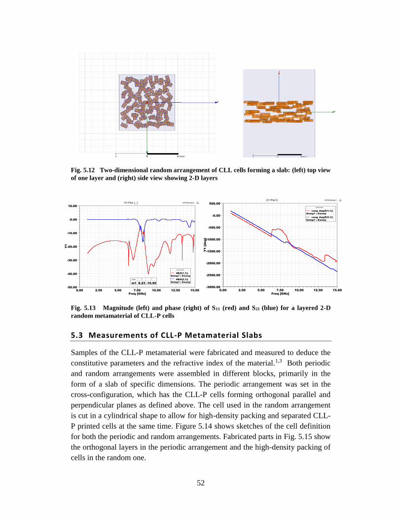
52
Fig. 5.12 Two-dimensional random arrangement of CLL cells forming a slab: (left) top view
of one layer and (right) side view showing 2-D layers
Fig. 5.13 Magnitude (left) and phase (right) of S11 (red) and S21 (blue) for a layered 2-D
random metamaterial of CLL-P cells
5.3 Measurements of CLL-P Metamaterial Slabs
Samples of the CLL-P metamaterial were fabricated and measured to deduce the
constitutive parameters and the refractive index of the material.1,3 Both periodic
and random arrangements were assembled in different blocks, primarily in the
form of a slab of specific dimensions. The periodic arrangement was set in the
cross-configuration, which has the CLL-P cells forming orthogonal parallel and
perpendicular planes as defined above. The cell used in the random arrangement
is cut in a cylindrical shape to allow for high-density packing and separated CLL-
P printed cells at the same time. Figure 5.14 shows sketches of the cell definition
for both the periodic and random arrangements. Fabricated parts in Fig. 5.15 show
the orthogonal layers in the periodic arrangement and the high-density packing of
cells in the random one.
0.00 2.50 5.00 7.50 10.00 12.50 15.00
Freq [GHz]
-50.00
-40.00
-30.00
-20.00
-10.00
-0.00
10.00
Y1
HFSSDesign1XY Plot 1_1 ANSOFT
m1
Curve Info
dB(S(1,1))
Setup1 : Sweep
dB(S(2,1))
Setup1 : Sweep
Name X Y
m1 8.23 -16.95
0.00 2.50 5.00 7.50 10.00 12.50 15.00
Freq [GHz]
-3000.00
-2500.00
-2000.00
-1500.00
-1000.00
-500.00
-0.00
500.00Y
1 [d
eg
]
HFSSDesign1XY Plot 5 ANSOFT
Curve Info
cang_deg(S(1,1))
Setup1 : Sweep
cang_deg(S(2,1))
Setup1 : Sweep

53
Fig. 5.14 Unit cell of fabricated CLL-P periodic (left) and random (right) metamaterial
with cut wire probes
Fig. 5.15 Picture of fabricated CLL-P metamaterial in periodic (top) and 3-D random
arrangements
A sketch of the experimental setup is shown in Fig. 5.16. A transmitter and
receiver are placed across from each other around a circular turntable that houses
the metamaterial slab. Narrow-beam horns are used on both sides to suppress
undesired interference and reflections. The metamaterial slab is surrounded by
sheets of absorbing material to limit the diffraction of the radiation from the
transmitter to the receiver. The rotation of the transmitter allows for testing the
material over a wide variation of incident angles. A picture of the setup is shown
in Fig. 5.17. An upper plate hinged to the lower plate of the turntable, and of the
same size, allows for creating a parallel plate waveguide environment for the
metamaterial testing.
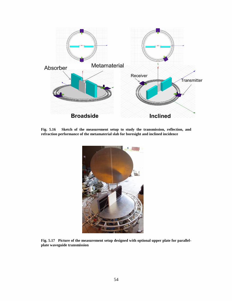
54
Fig. 5.16 Sketch of the measurement setup to study the transmission, reflection, and
refraction performance of the metamaterial slab for boresight and inclined incidence
Fig. 5.17 Picture of the measurement setup designed with optional upper plate for parallel-
plate waveguide transmission

55
The results reported in this subsection are for the case with the upper plate lifted,
as shown in Fig. 5.17, as the parallel plate environment was proven to be hard to
control with the plate sizes at the frequency of measurements.2 Scattering matrix
parameters, in an amplitude phase, were recorded and used to derive the refractive
index of the material and the corresponding constitutive parameters. The angular
location of the peak level of radiation as detected by the receive horn for different
inclined transmit angles was also used to determine the refractive index of the
material. Phase measurements were a key element in the accuracy of predicting
the constitutive parameters from the scattering matrix data. Samples of the
measured results are shown in Figs. 5.18 and 5.19 for the refractive index and
scattering parameters, respectively. This is shown for both periodic and random
metamaterials composed of CLL-P cells.
Fig. 5.18 Refractive index for periodic and random structures as deduced from measured
transmission and refraction phases
Fig. 5.19 Transmission parameter S21 for periodic and random slabs, showing the shift in
bandwidth

56
5.4 Remarks on Metamaterial Characterization
The characterization of metamaterials was performed through simulation and
measurements for both periodic and random arrangements of CLL and CLL-P
unit cells. As mentioned earlier, some of the results are not conclusive. Rigorous
electromagnetic analysis has been performed on general forms of metamaterial
cells.11–13 Comparison of such analysis and correlating it to the results shown here
are underway. Also, circuit models have been devised to analyze metamaterials.
This also needs to be performed for the CLL-P-based material.
Of interest is the phase response of propagation through the metamaterial. It is
conjectured that the unit cell structure causes the transmission phase to be large at
certain frequency bands.8 At inclined incidence, this translates in imposing steep
phase progression across the wavefront as the signal passes through the material.
The phase progression results in the creation of a grating lobe in the visible
region, hence the appearance of a beam in the negative refraction direction. This
is proven analytically using conventional array theories. A study of the presence
of this phase progression for the metamaterials in question is underway.
5.5 Application of CLL Metamaterials to Dipole Antenna Enhancement
As pointed out earlier, the CLL cells contribute to changing the permeability of
the medium. High-permeability material can form a surface or a block of
metamaterial that reflects a wave coherently at a small distance. This can be used
to produce a high-gain narrow beam from a conventional dipole.6,7,10 Two sides of
the CLL plane can act as a reflector and a director around the dipole in a fashion
similar to a Yagi-Uda array. If multiple planes are placed to surround the dipole,
as shown in Fig. 5.20, a sharp, high-gain beam results. The beam can be steered
mechanically by rotating the CLL structure around the dipole.
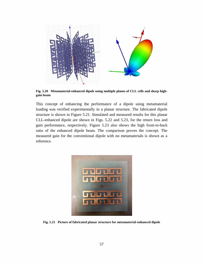
57
Fig. 5.20 Metamaterial-enhanced dipole using multiple planes of CLL cells and sharp high-
gain beam
This concept of enhancing the performance of a dipole using metamaterial
loading was verified experimentally in a planar structure. The fabricated dipole
structure is shown in Figure 5.21. Simulated and measured results for this planar
CLL-enhanced dipole are shown in Figs. 5.22 and 5.23, for the return loss and
gain performance, respectively. Figure 5.23 also shows the high front-to-back
ratio of the enhanced dipole beam. The comparison proves the concept. The
measured gain for the conventional dipole with no metamaterials is shown as a
reference.
Fig. 5.21 Picture of fabricated planar structure for metamaterial-enhanced dipole

58
Fig. 5.22 Simulated and measured S11 of the planar metamaterial-enhanced dipole
Fig. 5.23 Comparison of measured (green and black) vs. simulated (orange and dashed
blue) realized gain and front-to-back ratio of planar metamaterial-enhanced dipole;
conventional dipole is also plotted as a reference (dotted red)
-15-12
-9-6-30369
1.5 1.55 1.6 1.65 1.7 1.75 1.8 1.85 1.9 1.95 2
Re
aliz
ed
Gai
n [
dB
]
Frequency [GHz]
Front [Exp.] Back [Exp.] Dipole [Exp.]
59
5.6 References
1. Zaghloul AI, Lee YM, Anthony T, Weiss SJ. Measurements of
metamaterials in a parallel-plate waveguide medium. Antenna Applications
Symposium; 2011 Sep; Allerton, IL.
2. Lee Y, Zaghloul AI. Characterization of parallel-plate waveguides for
material measurements. URSI National Radio Science Meeting; 2012 Jan;
Boulder, CO.
3. Zagloul AI, Weiss SJ, Lee YM, Anthony TK. Characterization of
metamaterials through parallel-plate waveguide measurements. META’12.
3rd International Conference on Metamaterials, Photonic Crystals and
Plasmonics; 2012 Apr; Paris, France.
4. Hodge J II, Anthony TK, Zaghloul AI. Simulation and analysis of non-
periodic and random metamaterial structures. URSI National Radio Science
Meeting; 2014 Jan; Boulder, CO.
5. Talalai GA, Zaghloul AI. Problem formulation for randomized
metamaterials. CAP-CON; 2014 May; Chantilly, VA.
6. Hodge J II, Anthony TK, Zaghloul AI. Enhancement of the dipole antenna
using a capacitively loaded loop (CLL) structure. IEEE International
Symposium on Antennas and Propagation; 2014 Jul; Memphis, TN.
7. Hodge J II, Anthony TK, Zaghloul AI. Metamaterial loaded dipole antennas.
Antenna Applications Symposium; 2014 Sep; Allerton, IL.
8. Talalai GA, Garner TJ, Weiss SJ, Zaghloul AI. Relationship between phased
arrays and negative refraction. Applied Computational Electromagnetics
Society (ACES) Conference; 2015 Mar; Williamsburg, VA.
9. Hodge J II, Anthony TK, Zaghloul AI. Utilizing active circuit elements for
dynamic tuning and electronic scanning of CLL-loaded dipole antenna
structure. USNC-CNC/URSI Meeting; 2015 Jul; Vancouver, BC, Canada.
10. Hodge JA II, Anthony TK, Zaghloul AI. Metamaterial-loaded dipole
antenna. Invention disclosure, Pending, ARL, 2015.
11. Talalai GA. Metamaterial Modeling: S-parameter extraction method.
Technical Note, CERDEC, August 2013.
12. Talalai GA. Metamaterial modeling: quasi-static approximation. Technical
Note, CERDEC, March 2014.

60
13. Talalai GA. Macroscopic electromagnetic modeling. Technical Note,
CERDEC, March 2014.
14. Hhodge J II. Analysis of periodic and random capacitively-loaded loop
(CLL) metamaterial structures for antenna enhancement applications
[master’s thesis]. [Blacksburg (VA)]: Virginia Tech; 2014 May.
61
6. List of Publications, Patents, and Papers
Papers:
Zhou W, Dang G, Taysing-Lara M, Chang-Hasain C. Demonstration of a
slow-light high-contrast metastructure cage waveguide. Proceedings of the
SPIE Photonics West; 2013;8633:863305.
Zhou W, Dang G, Taysing-Lara M, Karagodsky V, Sun T, Chang-Hasnain
C. Slow-light high contrast metastructure hollow-core waveguides.
Proceedings of the SPIE Photonics West; 2012;8270–8.
Zhou W. Slow-light waveguide using high contrast gratings. Summary of
2012-International Nano-Electro-Optics Workshop; 2012.
Dang G, Taysing-Lara M, Zhou W. Loss measurements in silicon hollow-
core waveguides with metastructure high-contrast grating. Proceedings of
the 2012 Frontiers in Optics/Laser Science XXVIII (FiO/LS) Meeting;
2012.
Zaghloul AI. Active reflection phase surfaces for cognitive radar.
Proceeding URSI National Radio Science Meeting; 2013.
Hodge J II, Anthony TK, Zaghloul AI. Simulation and analysis of non-
periodic and random metamaterial structures. Proceeding URSI National
Radio Science Meeting; 2014.
Hodge J II, Anthony TK, Zaghloul AI. Enhancement of the dipole
antenna using a capacitively loaded loop (CLL) structure. Proceeding of
IEEE International Symposium on Antennas and Propagation; 2014.
Dang G, Taysing-Lara M, Zhou W, Sun T, Yang W, Chang-Hasnain C.
Design and fabrication of 3D high-contrast metastructure THz cage
waveguides. Proceedings of the SPIE Photonics West; 2015.
Sun T, Yang W, Zhou W, Chang-Hasnain C. Guided modes and slow
light in high contrast grating hollow core waveguide. Optical Society of
America, to be published.
Lee Y, Zaghloul AI. Characterization of parallel-plate waveguides for
material measurements, URSI National Radio Science Meeting; 2012 Jan;
Boulder, CO.

62
Zaghloul AI, Weiss SJ, Lee YM, Anthony TK. Characterization of
metamaterials through parallel-plate waveguide measurement. META’12;
3rd International Conference on Metamaterials, Photonic Crystals and
Plasmonics; 2012 Apr; Paris, France.
Talalai GA, Zaghloul AI. Problem formulation for randomized
metamaterials. CAP-CON; 2014 May; Chantilly, VA.
Hodge J II, Anthony TK, Zaghloul AI. Metamaterial loaded dipole
antennas. Antenna Applications Symposium; 2014 Sep; Allerton, IL.
Talalai A, Garner TJ, Weiss SJ, Zaghloul AI. Relationship between
phased arrays and negative refraction. Applied Computational
Electromagnetics Society (ACES) Conference; 2015 Mar; Williamsburg,
VA.
Hodge J II, Anthony TK, Zaghloul AI. Utilizing active circuit elements
for dynamic tuning and electronic scanning of CLL-loaded dipole antenna
structur. USNC-CNC/URSI Meeting; 2015 Jul; Vancouver, BC, Canada.
Presentations (incomplete list):
Dang G, Taysing-Lara M, Zhou W, Sun T, Yang W, Chang-Hasnain C.
Design and fabrication of 3D high-contrast metastructure THz cage
waveguides. Photonics West, 2015.
Zhou W, Dang G, Taysing-Lara M, Chang-Hasnain C. Demonstration of
a slow-light high-contrast metastructure cage waveguide. Photonics West,
8633-05, 2013.
Zhou W et al. Slow-light high contrast metastructure hollow-core
waveguides. Photonics West, 8270–8, 2012.
Zhou W. Slow-light waveguide using high contrast gratings. Summary of
2012 International Nano-Electro-Optics Workshop, 2012.
Chang-Hasnain C. High-contrast metastructures for integrated optics.
Opto Plenary Session, Photonics West, 2012.
Dang G, Taysing-Lara M, Zhou W. Loss measurements in silicon hollow-
core waveguides with metastructure high-contrast grating. Frontiers in
Optics/Laser Science XXVIII (FiO/LS) meeting. 2012 Oct 14–18;
Rochester, NY.
Zaghloul A. Active reflection phase surfaces for cognitive radar. NRSM
USNC-URSI Conference. 2013 Jan 8–11; Boulder, CO.
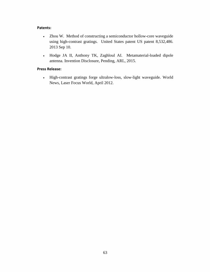
63
Patents:
Zhou W. Method of constructing a semiconductor hollow-core waveguide
using high-contrast gratings. United States patent US patent 8,532,486.
2013 Sep 10.
Hodge JA II, Anthony TK, Zaghloul AI. Metamaterial-loaded dipole
antenna. Invention Disclosure, Pending, ARL, 2015.
Press Release:
High-contrast gratings forge ultralow-loss, slow-light waveguide. World
News, Laser Focus World, April 2012.

64
1 DEFENSE TECH INFO CTR
(PDF) ATTN DTIC OCA
2 US ARMY RSRCH LAB
(PDF) ATTN IMAL HRA MAIL & RECORDS MGMT
ATTN RDRL CIO LL TECHL LIB
1 GOVT PRNTG OFC
(PDF) ATTN A MALHOTRA
8 US ARMY RSRCH LAB
(PDF) RDRL SE
G METCALFE
RDRL SEE E
G DANG
M TAYSING-LARA
W ZHOU
RDRL SER M
A ZAGHLOOL
RDRL WMM E
E NGO
M IVILL
D SHREIBER