metal-nitride-oxide-semiconductor light-emitting devices for...
TRANSCRIPT

Metal-nitride-oxide-semiconductor light-emitting devices for general lighting
Y. Berencén,1,* Josep Carreras,2 O. Jambois,1 J. M. Ramírez,1 J. A. Rodríguez,3 C. Domínguez,4 Charles E. Hunt,2,5 and B. Garrido1
1MIND-IN2UB, Dept. Electrònica, Universitat de Barcelona, Martí i Fanquès 1, 08028, Barcelona, Spain 2IREC, Catalonia Institute for Energy Research, Jardí de les Dones de Negre 1, PL2, 08930, Barcelona, Spain
3Physics Faculty, University of Havana, San Lázaro y L, Vedado, 10400 Havana, Cuba 4Instituto de Microelectrónica de Barcelona (IMB-CNM, CSIC), Bellaterra 08193, Barcelona, Spain
5California Lighting Technology Center,University of California 633 Peña Ave, Davis California, 95618, USA *[email protected]
Abstract: The potential for application of silicon nitride-based light sources to general lighting is reported. The mechanism of current injection and transport in silicon nitride layers and silicon oxide tunnel layers is determined by electro-optical characterization of both bi- and tri-layers. It is shown that red luminescence is due to bipolar injection by direct tunneling, whereas Poole-Frenkel ionization is responsible for blue-green emission. The emission appears warm white to the eye, and the technology has potential for large-area lighting devices. A photometric study, including color rendering, color quality and luminous efficacy of radiation, measured under various AC excitation conditions, is given for a spectrum deemed promising for lighting. A correlated color temperature of 4800K was obtained using a 35% duty cycle of the AC excitation signal. Under these conditions, values for general color rendering index of 93 and luminous efficacy of radiation of 112 lm/W are demonstrated. This proof of concept demonstrates that mature silicon technology, which is extendable to low-cost, large-area lamps, can be used for general lighting purposes. Once the external quantum efficiency is improved to exceed 10%, this technique could be competitive with other energy-efficient solid-state lighting options.
©2011 Optical Society of America
OCIS codes: (230.2090) Electro-optical devices; (150.2950) Illumination.
References and links
1. S. Nakamura, M. Senoh, and T. Mukai, “Highly P-Typed Mg-Doped GaN Films Grown with GaN Buffer Layers,” Jpn. J. Appl. Phys. 30(Part 2, No. 10A), 1708–1711 (1991).
2. F. A. Ponce and D. P. Bour, “Nitride-based semiconductors for blue and green light-emitting devices,” Nature 386(6623), 351–359 (1997).
3. S. Nakamura, M. Senoh, and T. Mukai, “High-power InGaN/GaN double-heterostructure violet light emitting diodes,” Appl. Phys. Lett. 62(19), 2390–2393 (1993).
4. S. Nakamura, M. Senoh, N. Shin-ichi, N. Iwasa, T. Yamada, T. Matsushita, Y. Sugimoto, and H. Kiyoku, “Room-temperature continuous-wave operation of InGaN multi-quantum-well structure laser diodes,” Appl. Phys. Lett. 69(26), 4056–4059 (1996).
5. A. Zukauskas, M. S. Shur, and R. Gaska, Introduction to Solid State Lighting (John Wiley and Sons, New York, 2002).
6. E. F. Schubert and J. K. Kim, “Solid-state light sources getting smart,” Science 308(5726), 1274–1278 (2005). 7. Photonics 21 Strategic Research Agenda, http://www.photonics21.org/AboutPhotonics21/SRA.php 8. Multi-Year Program Plan, Solid State Lighting Research and Development, US Department of Energy,
http://apps1.eere.energy.gov/buildings/publications/pdfs/ssl/ssl_mypp2009_web.pdf 9. Y.-L. Wang, F. Ren, H. S. Kim, D. P. Norton, and S. J. Pearton, F. Ren, D. P. Norton, and S. J. Pearton,
“Materials and Process Development for ZnMgO/ZnO Light-Emitting Diodes,” IEEE J. Quantum Electron. 14(4), 1048–1052 (2008).
10. W. I. Park and G.-C. Yi, “Electroluminescence in n-ZnO Nanorod Arrays Vertically Grown on p-GaN,” Adv. Mater. (Deerfield Beach Fla.) 16(1), 87–90 (2004).
#141485 - $15.00 USD Received 20 Jan 2011; revised 10 Mar 2011; accepted 11 Mar 2011; published 29 Mar 2011(C) 2011 OSA 9 May 2011 / Vol. 19, No. S3 / OPTICS EXPRESS A234

11. L. T. Canham, “Silicon quantum wire array fabrication by electrochemical and chemical dissolution of wafers,” Appl. Phys. Lett. 57(10), 1046–1048 (1990).
12. L. Pavesi, L. Dal Negro, C. Mazzoleni, G. Franzò, and F. Priolo, “Optical gain in silicon nanocrystals,” Nature 408(6811), 440–444 (2000).
13. R. J. Walters, G. I. Bourianoff, and H. A. Atwater, “Field-effect electroluminescence in silicon nanocrystals,” Nat. Mater. 4(2), 143–146 (2005).
14. T. P. Chen, Y. Liu, M. S. Tse, O. K. Tan, P. F. Ho, K. Y. Liu, D. Gui, and A. L. K. Tan, “Dielectric functions of Si nanocrystals embedded in a SiO2 matrix,” Phys. Rev. B 68(15), 153301 (2003).
15. J. Bu and M. H. White, “Design considerations in scaled SONOS nonvolatile memory devices,” Solid-State Electron. 45(1), 113–120 (2001).
16. M. Perálvarez, C. García, M. López, B. Garrido, J. Barreto, C. Domínguez, and J. A. Rodríguez, “Field effect luminescence from Si nanocrystals obtained by plasma-enhanced chemical vapor deposition,” Appl. Phys. Lett. 89(5), 051112–051115 (2006).
17. O. Jambois, Y. Berencen, K. Hijazi, M. Wojdak, A. J. Kenyon, F. Gourbilleau, R. Rizk, and B. Garrido, “Current transport and electroluminescence mechanisms in thin SiO2 films containing Si nanocluster-sensitized erbium ions,” J. Appl. Phys. 106(6), 063526–063532 (2009).
18. J. F. Ziegler, J. P. Biersack, and U. Littmark, The Stopping and Range of Ions in Solids (Pergamon, New York, 1985).
19. M. Perálvarez, J. Barreto, J. Carreras, A. Morales, D. Navarro-Urrios, Y. Lebour, C. Domínguez, and B. Garrido, “Si-nanocrystal-based LEDs fabricated by ion implantation and plasma-enhanced chemical vapour deposition,” Nanotechnology 20(40), 405201 (2009).
20. S. M. Sze, Physics of Semiconductor Devices 2nd ed. (Wiley, New York, 1981). 21. S. Habermehl, R. T. Apodaca, and R. J. Kaplar, “On dielectric breakdown in silicon-rich silicon nitride thin
films,” Appl. Phys. Lett. 94(1), 012905–012908 (2009). 22. W. Chandra and L. K. Ang, “Space charge limited current in a gap combined of free space and solid,” Appl.
Phys. Lett. 96(18), 183501 (2010). 23. J. Warga, R. Li, S. N. Basu, and L. Dal Negro, “Electroluminescence from silicon-rich nitride/silicon superlattice
structures,” Appl. Phys. Lett. 93(15), 151116 (2008). 24. R. Hattori and J. Shirafuji, “Longitudinal electron drift mobility of hydrogenated amorphous silicon/silicon
nitride multilayer structures revelealed by time-of-flight measurements,” Appl. Phys. Lett. 54(12), 1118–1120 (1989).
25. J. Robertson and M. J. Powell, “Gap states in silicon-nitride,” Appl. Phys. Lett. 44(4), 415–417 (1984). 26. Z. H. Cen, T. P. Chen, Z. Liu, Y. Liu, L. Ding, M. Yang, J. I. Wong, S. F. Yu, and W. P. Goh, “Electrically
tunable white-color electroluminescence from Si-implanted silicon nitride thin film,” Opt. Express 18(19), 20439–20444 (2010).
27. L. Dal Negro, J. H. Yi, L. C. Kimerling, S. Hamel, A. Williamson, and G. Galli, “Light emission from silicon-rich nitride nanostructures,” Appl. Phys. Lett. 88(18), 183103 (2006).
28. K. A. Nasyrov, S. S. Shaimeev, and V. A. Gritsenko, “Trap-Assisted Tunneling Hole Injection in SiO2: Experiment and Theory,” J. Exp. Theor. Phys. 109(5), 786–793 (2009).
29. M. Perálvarez and J. Josep Carreras, M. Perálvarez, J. Carreras, J. Barreto, A. Morales, C. Domínguez, and B. Garrido, “Efficiency and reliability enhancement of silicon nanocrystal field-effect luminescence from nitride-oxide gate stacks,” Appl. Phys. Lett. 92(24), 241104 (2008).
30. CIE, (1995), Method of Measuring and Specifying Colour Rendering Properties of Light Sources Publication 13.3, Vienna: Commission Internationale de l'Eclairage, ISBN 978–3900734572.
31. CIE, (1926), Commission internationale de l'Eclairage proceedings (Cambridge University Press, Cambridge) p. 1924.
32. W. Davis and Y. Ohno, “Color quality scale,” Opt. Eng. 49(3), 033602 (2010). 33. J. Carreras, J. M. Quintero, and C. E. Hunt, “Theoretical limits of natural light emulation,” Second CIE Expert
Symposium on Appearance, Ghent, Belgium (2010). 34. J. Carreras, J. Quintero, and C. E. Hunt, “Towards the Definition of New Visual Color Quality Representations,”
Illuminating Engineering Society (IES) Meeting, Toronto, Canada, (2010).
1. Introduction
The luminous efficacy of Solid State Light (SSL) sources has soared in the last decade from a few lm/W (less than incandescent bulb) to astonishing values in excess of 150 lm/W (superior to high-pressure Na lamps). This has been largely due to the development of III-V nitride compound technology (GaN, GaInN, AlGaN, AlGaInN) in the 90’s, with breakthroughs such as the attainment of p-type doping in GaN [1,2] and the subsequent demonstration of blue and green GaInN double-heterostructure, high-power LEDs and lasers [3,4]. Further improvements in doping, reduction of dislocation density, improved thermal management and the use of multiple quantum wells have made possible the fabrication of high-power LEDs with ever increasing efficacies and emitted power, making them promising for lighting
#141485 - $15.00 USD Received 20 Jan 2011; revised 10 Mar 2011; accepted 11 Mar 2011; published 29 Mar 2011(C) 2011 OSA 9 May 2011 / Vol. 19, No. S3 / OPTICS EXPRESS A235
purposes [5]. Nevertheless, LEDs are quite monochromatic light sources and, their use as white lighting sources requires wavelength conversion either by phosphors or semiconductor wavelength converters [5]. Large Stokes losses (i.e. higher-energy photons are converted into lower-energy photons), integration with phosphor packaging and color drift are limitations of this approach. Other approaches for white-light emission use multicolored LEDs (tri-chromatic and tetra-chromatic) together with color mixing optics. The absence of Stokes loss and good color rendering are promising features, whereas the poor efficiency in current green LEDs, and the color drift of red AlGaInP LEDs, give poor color mixing and low overall efficacy [6]. Normally, the addition of more wavelengths by adding more LED sources facilitates better adjustment of color temperature and color rendering, but this is accomplished at the expense of efficacy, stability and increased cost.
SSL sources for general lighting could save enormous amounts of energy as about 20% of all electricity is consumed for lighting purposes. Environmental savings, in terms of less green-house (CO2) and poisonous gas emissions (e.g. containing Hg), would also be major benefits [7,8]. Although nitride compound technology has made possible the introduction of SSL, its massive deployment is hampered by the significant cost inherent to III-V technologies and the lack of a suitable substrate for mass fabrication. Additionally, III-V technology does not provide simple routes for integrated white-light emitters without the use of phosphor converters. While organic LEDs (OLEDs) can be made cheaper and have suitable substrates, they are mainly used for diffuse areal lighting in large area devices. Some other disruptive approaches have been proposed such as ZnMgO on ZnO substrates [9] and GaN and ZnO nanowires on cheap substrates [10]. These last approaches circumvent the need of expensive sapphire substrates. However, they still require expensive epitaxial reactors for fabrication.
A new and disruptive approach towards Solid State Lighting is presented here. It is suitable for developing white-light monolithically integrated emitters for lighting purposes. This approach, that we call “Silicon-based Lighting (SiL),” is based on the employment of novel SSL procedures using Silicon and CMOS (or large-area a-Si compatible technology) in its manufacturing. This is accomplished by merging the experience gained from both Silicon Photonics and Solid State Lighting Technology. The scalability, cost-effectiveness and mass-production potential already demonstrated by the silicon semiconductor industry would enable reduced costs and significant penetration of energy-efficient solutions in the marketplaces where nitrided-semiconductor LEDs are challenged for economical massive deployment.
Si-based integrated light sources were first reported in the early 90’s, after the discovery of porous silicon and Si-nanocrystals/nanoclusters (Si-nc) visible emission [11–13]. Nanostructuring Silicon produces a dramatic increase in luminescent emission because of quantum confinement of excitons in Si-nc. Confinement brings about relaxation of selection rules for radiative transitions in indirect band-gap silicon. Furthermore, band-gap enlargement dependency on Si-nc size makes possible the tuning of the emission in the red-orange part of the visible spectrum. A suitable matrix that passivates non-radiative centers in Si-nc, and promotes conduction, is desirable for device manufacturability as well as for large internal quantum efficiency of electroluminescence (EL). SiOx (Silicon Rich Silicon Oxide, SRSO) has been thoroughly studied as a suitable matrix for Si-nc [11–14]. Nevertheless, Si-nc embedded in SiNx (Silicon Rich Silicon Nitride, SRSN) has emerged as an alternative for its superior transport properties and better color rendering. By combining red-orange emission of Si-nc in SiOx with green-blue emission of Si-nc in SiNx we have been able of synthesizing a white light emitting efficient EL material. Although efficacy for the moment remains quite low in our LEDs (less than 1 lm/W), there is room for orders of magnitude of improvement by optimizing the material, improving charge injection and transport, and enhancing extraction efficiency. We believe that this route for developing efficient light sources will eventually become successful, provided the efficacy of devices nears that of existing OLEDs (5-10 lm/W). Silicon or glass wafers are low-cost suitable substrate material for these devices. In
#141485 - $15.00 USD Received 20 Jan 2011; revised 10 Mar 2011; accepted 11 Mar 2011; published 29 Mar 2011(C) 2011 OSA 9 May 2011 / Vol. 19, No. S3 / OPTICS EXPRESS A236
addition, Si-based materials open the possibility of integrating LEDs with drivers and control in the same chip, making affordable the concept of System on Chip (SoC) lighting. Economical deposition technology is available in CMOS foundries and large area devices can be fabricated -with application to areal lighting- in a way similar than for solar cells.
In this investigation, we present a metal-nitride-oxide-semiconductor light-emitting device (MNOSLED) as a proof of concept for “Silicon-based Lighting” (SiL). These first non-optimized MNOSLEDs are driven as MOS capacitors and transistors. Experimental details and electrical and electro-optical studies are presented in Sections 2 and 3, respectively. Photometric analysis of the MNOSLED is presented in section 4, including color rendering, color quality and luminous efficacy of radiation. The emphasis is to assess the applicability of this device as a potentially low-cost, high-quality SSL white-light source.
2. Experimental details
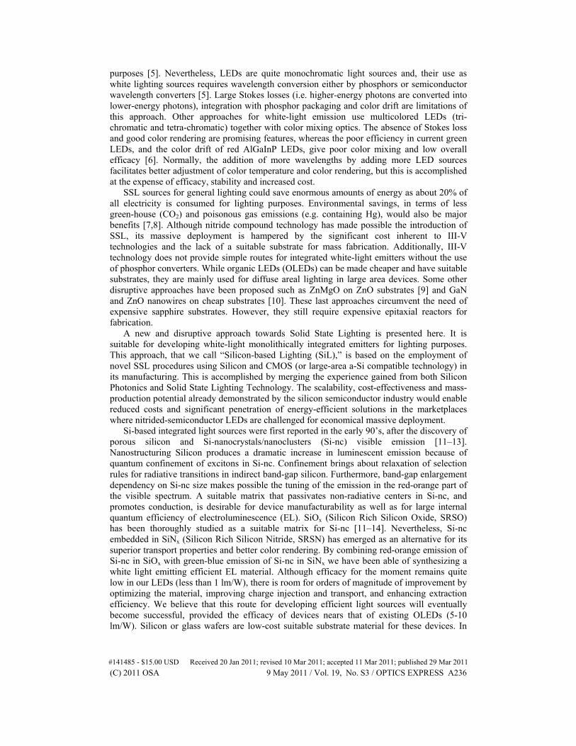
Generally speaking, we define a MOSLED as a metal-oxide-semiconductor field-effect capacitor or transistor (MOSFET) with a transparent gate electrode. The ‘oxide’, depending on design and material properties, is frequently substituted by a gate stack or a composite material, although we use to maintain the MOSLED name. For the particular type of device presented here we also use the term MNOSLED to enhance the fact that we have introduce a bi-layer (or tri-layer) in a similar way as for the MNOS memories [15]. The electrodes used in previous designs include semitransparent metals, thin polysilicon and indium tin oxide (ITO) [16,17]. The electrode preferred in current devices is a thin (100 nm), semitransparent n-type (phosphorous) heavily-doped polysilicon. This choice emphasizes compatibility; and for this reason the devices have been entirely fabricated in a standard CMOS line. The drawback of using a thin 100 nm polysilicon gate is its varying (non-flat) transmission in the visible spectrum due to a Fabry-Perot interference pattern and its low transmission in the blue [16]. Two dielectric or gate stack structures have been designed and fabricated in this investigation, as depicted in Fig. 1(a). The first one is a bi-layer of very thin tunneling silicon oxide (3 nm) and a silicon nitride transport layer (26 nm). The second one is a tri-layer which includes an extra-thin silicon oxide layer (3 nm) on top of the previous structure. The purpose of the thin oxide layers is to provide a well-passivated interface with silicon, and to act as tunnel and control dielectrics for the current (hole and electron injection) in the central thick nitride layer.
Fig. 1. (a) Cross-sectional view of the two Silicon Nitride MNOSLED structures under study. A1: Tunnel oxide (SiO2) + Si3N4 and A2: Tunnel oxide (SiO2) + Si3N4 + control oxide (SiO2). (b) Top view of a typical device. The semi-transparent gate electrode is the central rectangle with dimensions 10µm x 500 µm.
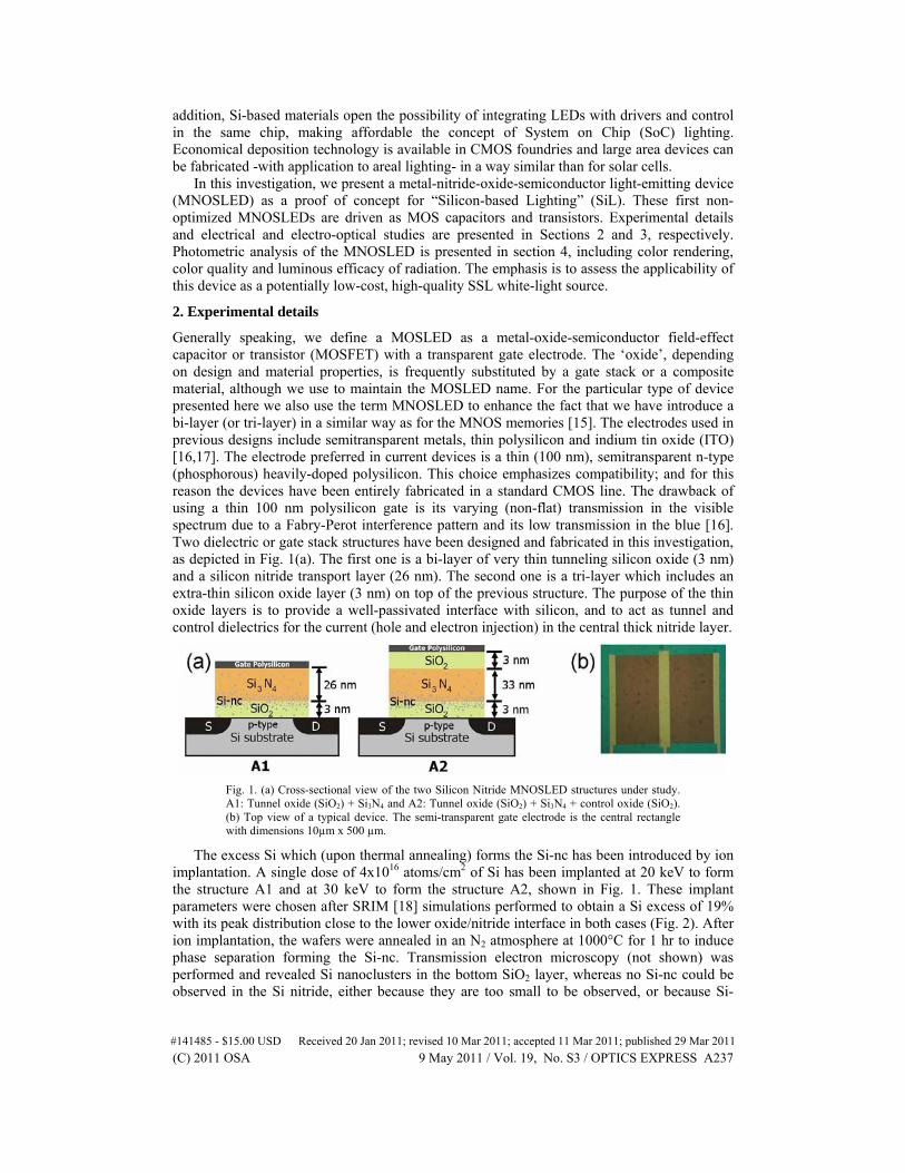
The excess Si which (upon thermal annealing) forms the Si-nc has been introduced by ion implantation. A single dose of 4x10¹⁶ atoms/cm2 of Si has been implanted at 20 keV to form the structure A1 and at 30 keV to form the structure A2, shown in Fig. 1. These implant parameters were chosen after SRIM [18] simulations performed to obtain a Si excess of 19% with its peak distribution close to the lower oxide/nitride interface in both cases (Fig. 2). After ion implantation, the wafers were annealed in an N2 atmosphere at 1000°C for 1 hr to induce phase separation forming the Si-nc. Transmission electron microscopy (not shown) was performed and revealed Si nanoclusters in the bottom SiO2 layer, whereas no Si-nc could be observed in the Si nitride, either because they are too small to be observed, or because Si-
#141485 - $15.00 USD Received 20 Jan 2011; revised 10 Mar 2011; accepted 11 Mar 2011; published 29 Mar 2011(C) 2011 OSA 9 May 2011 / Vol. 19, No. S3 / OPTICS EXPRESS A237
based defects are more likely to be created in Si nitrides. Additionally, the top control oxide in A2 is completely free of Si-nc and should act as a current-flow limiting layer.
The Source/Drain regions of the n-channel MNOSLEDs were formed by phosphorous implantation. The thin polysilicon gate electrode was deposited by low-pressure chemical vapour deposition (LPCVD) at 780°C and degenerately doped with POCl3. The process sequence employed standard MOS procedures, resulting in the final transistor structure, as seen (top view) in Fig. 1(b). P-type silicon substrates were used for both structures.
Fig. 2. SRIM simulation profile for each structure.
Quasi-static current-voltage (I-V) measurements were performed using a semiconductor parameter analyzer (Agilent B1500A) with high-power/high-resolution units coupled to a probe station (Cascade Microtech Summit 11000) using Faraday isolation (microchamber). The devices are forward biased, that is, a negative voltage is applied to the gate. This corresponds to an accumulation regime in the p-type Si substrate. As seen later, this enables the activation of the Si-nc in the SRSO layer that are expected to emit in the red [13,16]. The microchamber was optically coupled to a long working distance Mitutoyo objective. The EL spectra in AC excitation were obtained by applying a square waveform to the gate by means of an Agilent 8114A Pulse Generator. Thus, light emitted by the devices was then conducted to an Acton 2300i grating spectrometer for analysis and detection by a cryogenically-cooled PI Spec-10-100B/LN charge-coupled device. Device emission spectra were corrected using the optical transfer function of the system, calibrated with measurements from a white-emission Xe lamp.
3. Electro-optical characterization
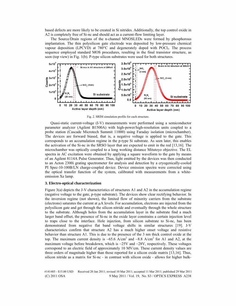
Figure 3(a) depicts the J-V characteristics of structures A1 and A2 in the accumulation regime (negative voltage to the gate, p-type substrate). The devices show clear rectifying behavior. In the inversion regime (not shown), the limited flow of minority carriers from the substrate (electrons) saturates the current at µA levels. For accumulation, electrons are injected from the polysilicon gate and get through the silicon nitride and eventually through the whole structure to the substrate. Although holes from the accumulation layer in the substrate find a much larger band offset, the presence of Si-nc in the oxide layer constrains a certain injection level to traps close to the interface. Hole injection, from silicon substrate to Si-nc, has been demonstrated from negative flat band voltage shifts in similar structures [19]. J-V characteristics confirm that structure A2 has a much higher onset voltage and resistive behavior than structure A1. This is due to the presence of the 3 nm thick control oxide at the top. The maximum current density is 65.6 A/cm2 and 8.8 A/cm2 for A1 and A2, at the maximum voltage before breakdown, which is 25V and 28V, respectively. These voltages correspond to an electric field of approximately 10 MV/cm. These current density values are three orders of magnitude higher than those reported for a silicon oxide matrix [13,16]. Thus, silicon nitride as a matrix for Si-nc - in contrast with silicon oxide - allows for higher bulk-
#141485 - $15.00 USD Received 20 Jan 2011; revised 10 Mar 2011; accepted 11 Mar 2011; published 29 Mar 2011(C) 2011 OSA 9 May 2011 / Vol. 19, No. S3 / OPTICS EXPRESS A238
limited currents (higher conductivity) and higher injection-limited currents (lower band offsets with Si).
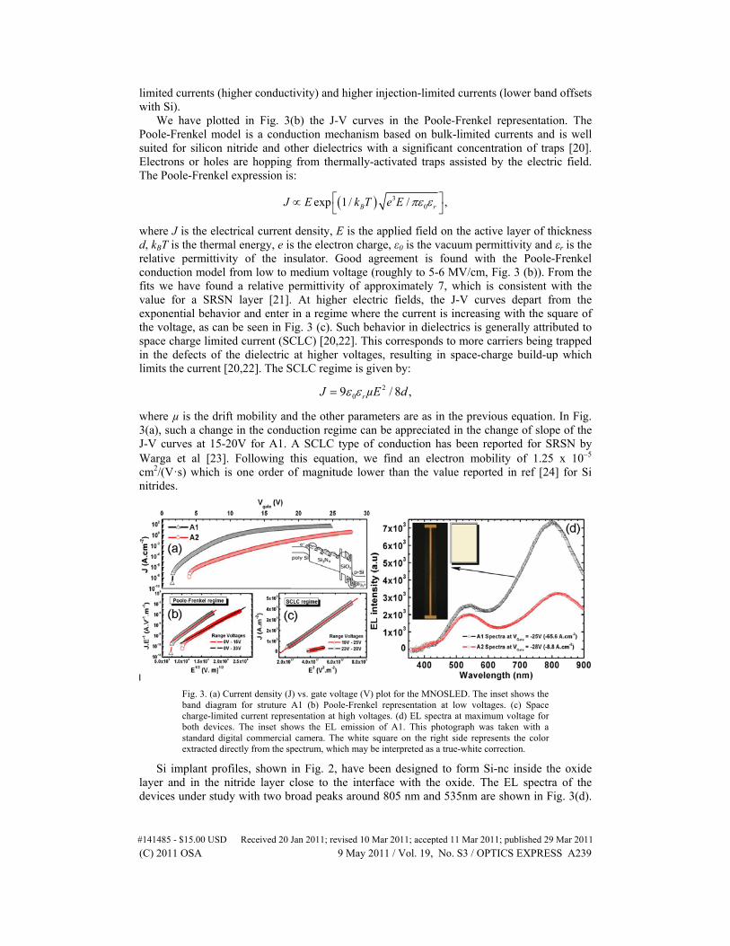
We have plotted in Fig. 3(b) the J-V curves in the Poole-Frenkel representation. The Poole-Frenkel model is a conduction mechanism based on bulk-limited currents and is well suited for silicon nitride and other dielectrics with a significant concentration of traps [20]. Electrons or holes are hopping from thermally-activated traps assisted by the electric field. The Poole-Frenkel expression is:
30exp 1/ / ,
B rJ E k T e E
where J is the electrical current density, E is the applied field on the active layer of thickness d, kBT is the thermal energy, e is the electron charge, ε0 is the vacuum permittivity and εr is the relative permittivity of the insulator. Good agreement is found with the Poole-Frenkel conduction model from low to medium voltage (roughly to 5-6 MV/cm, Fig. 3 (b)). From the fits we have found a relative permittivity of approximately 7, which is consistent with the value for a SRSN layer [21]. At higher electric fields, the J-V curves depart from the exponential behavior and enter in a regime where the current is increasing with the square of the voltage, as can be seen in Fig. 3 (c). Such behavior in dielectrics is generally attributed to space charge limited current (SCLC) [20,22]. This corresponds to more carriers being trapped in the defects of the dielectric at higher voltages, resulting in space-charge build-up which limits the current [20,22]. The SCLC regime is given by:
209 / 8 , rJ µE d
where µ is the drift mobility and the other parameters are as in the previous equation. In Fig. 3(a), such a change in the conduction regime can be appreciated in the change of slope of the J-V curves at 15-20V for A1. A SCLC type of conduction has been reported for SRSN by Warga et al [23]. Following this equation, we find an electron mobility of 1.25 x 105 cm2/(V·s) which is one order of magnitude lower than the value reported in ref [24] for Si nitrides.
Fig. 3. (a) Current density (J) vs. gate voltage (V) plot for the MNOSLED. The inset shows the band diagram for struture A1 (b) Poole-Frenkel representation at low voltages. (c) Space charge-limited current representation at high voltages. (d) EL spectra at maximum voltage for both devices. The inset shows the EL emission of A1. This photograph was taken with a standard digital commercial camera. The white square on the right side represents the color extracted directly from the spectrum, which may be interpreted as a true-white correction.
Si implant profiles, shown in Fig. 2, have been designed to form Si-nc inside the oxide layer and in the nitride layer close to the interface with the oxide. The EL spectra of the devices under study with two broad peaks around 805 nm and 535nm are shown in Fig. 3(d).
#141485 - $15.00 USD Received 20 Jan 2011; revised 10 Mar 2011; accepted 11 Mar 2011; published 29 Mar 2011(C) 2011 OSA 9 May 2011 / Vol. 19, No. S3 / OPTICS EXPRESS A239

The inset of Fig. 3(d) shows a photograph of the MNOSLED device (A1) with the emitted orange-white light. A bi-layer or tri-layer structure like those reported here are expected to have red-infrared luminescence from Si-nc in the oxide and/or nitride and blue-green luminescence of Si based defects in the silicon nitride [19,25,26]. Note that when silicon precipitates have been observed (by electron microscopy) in a silicon nitride matrix, red emission is reported as well [23]. However, in our case, Si-ncs have not been observed into silicon nitride. Consequently, the peak around 535 nm is attributed to the luminescence of the SRSN. In particular, it has been reported that luminescent centers associated to defects, such as Si-dangling bonds located in the middle of the band-gap, as well as bonding states of Si-Si units that are close to the valence band edge, emit at this wavelength [25,26]. In similar layers, luminescence lifetimes in the ns and µs range are ascribed to silicon nitride defects and Si-nc into silicon oxide matrix, respectively, according to dynamic studies reported [19,27]. It should also be noted that the transmittance spectrum of a 100 nm thick polysilicon layer has resonances at 470 nm and 760 nm. Therefore, it is expected that the measured spectra are reinforced at those frequencies. Transparent conducting oxides (TCO) will be used in subsequent optimized devices.
It is desired to emit light using the mechanism of excitation of the luminescent centers (Si-nc in oxide and Si-defects in nitride). It is extremely important to engineer the active material to enhance radiative recombination and/or decrease non-radiative recombination and thus optimize the internal quantum efficiency (IQE). Excitation efficiency of luminescent centers is closely related to the mechanism of injection. Tunnel bipolar injection of electrons and holes from opposite electrodes into Si-nc is an efficient way to create excitons in Si-nc from cold carriers. This tunnel injection is expected for a defective layer where the Poole-Frenkel mechanism of conduction takes place, and is attributed to the excitation mechanism of Si-nc in SRSO and defects in SRSN. Electrons do travel by Poole-Frenkel from the poly gate to the Si-nc and defects in the oxide and nitride, while holes are injected into a few nanometers of the SRSO by tunneling from the accumulation layer in the p-type Si substrate (see inset of Fig. 3(a)) [19,28]. To add in favor of this, when we bias the structure in inversion, only the green-blue peak is detected. This is clearly due to the lack of injected holes from the gate electrode. With regards to the emission from Si-related defects in SRSN, the injected electrons activate the luminescent centers by Poole-Frenkel ionization. The two different structures analyzed in this work only differ in external quantum efficiency (EQE). The relative intensity of the red and green bands is related to the details of the Si-excess profile in the nitride/oxide bi-layer and can be tailored due to photometric requirements, as we will demonstrate in the next section. The best emitting devices obtained, thus far, belongs to a series of bi-layer devices emitting in the red, with almost negligible Si-excess in the nitride layer and a peak up to 0.1% power efficiency which corresponds to a 1% EQE [29].
4. Photometric characterization
In order to investigate the potential impact of this technology as a candidate to replace mainstream lighting, the photometric characteristics have to be analyzed in-depth. In particular, we are interested in the determination of color rendering and quality as well as in the overall efficacy of such a device. Although the former can be straightforwardly analyzed by using standard CIE color rendering metrics for broadband sources, like general color rendering index (CRI) [30], the latter is not easy to determine, because of the impossibility to presently evaluate all of the potential available for improvement in the external quantum efficiency which exists for this technology.
Considering that a lighting device’s total wall-power to illuminant efficiency, η, is the product of multiple efficiency elements, e.g. η = Π ηi, Luminous Efficacy of Radiation (LER) is one of the critical multiplicative factors affecting η of a source. In this section, we restrict our energy analyses to the study of LER, which means that we are leaving aside other energy loss mechanisms occurring inside the device such as non-radiative recombination, charge
#141485 - $15.00 USD Received 20 Jan 2011; revised 10 Mar 2011; accepted 11 Mar 2011; published 29 Mar 2011(C) 2011 OSA 9 May 2011 / Vol. 19, No. S3 / OPTICS EXPRESS A240

injection, light extraction (that were treated in the preceding sections), as well as external factors such as power-supply efficiency.
In order to maximize LER, it would be ideal to keep the spectral content of the light source in a small region around 555 nm, where the sensitivity of the human eye peaks according to the CIE Luminosity Function [31]. However, doing so limits the color span that the source can correctly render. Obviously, the choice to prioritize energy efficiency or color reproduction depends ultimately upon the particular application under consideration. In Fig. 4 are shown the spectra obtained under different excitation conditions that involve changes in excitation voltage (Fig. 4(a)), period of the excitation signal (Fig. 4(b)), and duty cycle of the excitation signal (Fig. 4(c)). Moreover, the right columns in the same plot show color trajectories in the CIE 1931 diagram that are experienced under these excitation changes.
The XYZ CIE 1931 diagram is a color map that contains all the perceivable colors to humans. Blackbody radiators, such as the sun and other hot objects, including flames, are considered natural. This means that the color coordinates of any artificial light source intended for general lighting should lie very close to the blackbody locus plotted in dotted white lines in the CIE diagrams of Fig. 4. The tolerance of deviation from the blackbody locus is usually measured in the U*V*W* space by a distance termed ∆uv (or simply Duv), and usually the general rule of Duv<0.0054 is applied for white light sources targeting natural appearance. However, this is not an absolute requirement, since it has been argued that slight out-of-blackbody-locus illumination is acceptable, as long as it is supported by color preference schemes in detriment of naturalness of the light source [32].
Fig. 4. Color shifts in the CIE 1931 diagram produced under a change in (a) excitation voltage (T = 10µs and DC = 50%), (b) period of the excitation signal (V = 25V and DC = 50%) and (c) duty cycle of the excitation signal (V = 25V and T = 10µs).
#141485 - $15.00 USD Received 20 Jan 2011; revised 10 Mar 2011; accepted 11 Mar 2011; published 29 Mar 2011(C) 2011 OSA 9 May 2011 / Vol. 19, No. S3 / OPTICS EXPRESS A241

The most remarkable fact derived from the XY trajectories followed under different excitation conditions, is that important color shifts can only be obtained by changing the voltage amplitude of the excitation waveform. This procedure gives rise to a Correlated Color Temperature (CCT) span of 3310K, from 4385K to 7695K, covering a great number of important applications in lighting (“normal white” being considered CCT = 5500K). However, it does not cover the interesting warm CCT of around 3000K that is typical of the omnipresent incandescent light bulb. This warmer white could be easily worked out through the material’s optimization by slightly shifting the peak centered at 535nm towards the red region.
As shown in the detailed photometric study of the spectra set in Fig. 5, changes of 90% in the duty cycle (DC), allow only modest changes in the perceived CCT, covering the range between 4500K and 5000K. It is worth noting that this occurs without a substantial change in Duv, thus preserving the naturalness of the original spectrum. In other words, time-related changes in the excitation waveform lead to modest shifts in color but preserve Duv or “follow” the blackbody locus, while changes in the excitation voltage give rise to notable color shifts but at the expense of bringing about instabilities in the naturalness of the light produced.
Fig. 5. Dependence of Correlated Color Temperature (CCT), deviation from the blackbody locus (DUV), Luminous Efficacy of Radiation (LER) and Color Rendering Index (CRI) on Voltage (a) and on Duty Cycle (b).
In addition to control of spectral content, the present international energy-conservation effort mandates the consideration of the luminous efficacy of radiation or LER. At the same time, LER optimization alone cannot result in a light source which correctly reproduces colors, because low acceptance by the public would limit its market penetration. Recent studies have established theoretical limits up to where these two inversely correlated variables can be jointly optimized [33]. These studies demonstrate that for [3000K,5500K,8000K] spectra, it is physically possible to obtain efficacies of [363,313,288] lm/W while maintaining general CRIs over 90, ensuring outstanding light quality within the most important regions of the Munsell gamut.
These theoretical values indicate that efficacies shown in the second column plots of Fig. 5 can be substantially enhanced by optimizing the materials to emit only in the visible range,
#141485 - $15.00 USD Received 20 Jan 2011; revised 10 Mar 2011; accepted 11 Mar 2011; published 29 Mar 2011(C) 2011 OSA 9 May 2011 / Vol. 19, No. S3 / OPTICS EXPRESS A242

eliminating the loss of efficacy that arises from the near-infrared portion of the spectra shown in Fig. 4 as was mentioned in the section 3.
Similar to what is observed with color shifts (CCTs), the dependence of CRI and efficacy on voltage, is much stronger than on duty cycle. In addition, luminous efficacies as high as 112 lm/W and general CRIs above 93 are achievable for DCs of 35%. By analyzing in detail this optimized spectrum of about CCT = 4800K, we can further evaluate up to what extent it would render colors in a wide color gamut by utilizing the so-called Color Rendering Map (CRM) presented elsewhere [34]. In Fig. 6, a set of scores are represented by color-coding (from blue to red, corresponding to Rm values from 0 to 100) and plotting over a tracing of the Munsell gamut area of an original CIE 1931 color-space chart as illustrated in the inset of Fig. 6(b). The plot created by these scores represents the most significant saturation levels and hues, as defined in the Munsell color system. This system is widely accepted by both the display and lighting communities. For the Reader’s reference, the Munsell gamut color space, around the CIE white point from the CIE 1931 chart, is depicted in Fig. 6(a). From it, the identification of the color that a particular score represents (visually depicted in the color bar of the Fig. 6(b)) is directly found by comparison.
Fig. 6. (a) Musell region in the CIE 1931 diagram. (b) Color Rendering Map (CRM) of the spectrum excited through a waveform of 25V amplitude, 10µs period and 35% duty cycle.
By direct inspection, one sees that the optimized 4800K spectrum that has an general CRI of 93, presents good color rendering all along the Munsell region, always satisfying Rm>80 no matter what color is trying to reproduce. This is indeed the most convincing argument that enables us to conclude that the light produced by MNOSLEDs with Si3N4 and Si nanocrystals fulfills all the requirements required in the lighting industry in terms of color rendition and quality.
The external quantum efficiency of all-silicon light sources represents, at this time, the most important challenge. In fact, although the promise of omnipresent and high color quality silicon lighting is quite appealing because of the price reduction, integration, large area, etc., the small wall-plug (W) to light (W) efficiency in this technology is clearly the most limiting factor that prevents its general application at this point. The fact the emission spectrum can be adjusted depending on particular needs through material and/or device engineering indicates that superior LER than in the results presented here can be achieved.
For the sake of illustration, if the target total efficacy for this technology was fixed to 30 lm/W, to compete with commercial OLEDs, assuming a LER of approximately 300 lm/W would indicate that external quantum efficiencies near 10% would be required. This requires a challenging one order of magnitude increase, minimum, in the emission efficiency. It is worth noting that the spectral content can potentially be narrowed to the visible region by means of material’s optimization (basically by eliminating part of the near-infrared tail produced by the
#141485 - $15.00 USD Received 20 Jan 2011; revised 10 Mar 2011; accepted 11 Mar 2011; published 29 Mar 2011(C) 2011 OSA 9 May 2011 / Vol. 19, No. S3 / OPTICS EXPRESS A243

Si nanocrystals EL), so that it is realistic to anticipate that the LER could be increased up to 300 lm/W, without a detriment in color quality.
5. Conclusion
We have presented in this work some potential of silicon-based white-lighting SSL devices for general lighting. From the two structures studied, the SiO2 + Si3N4 bilayer structure shows better electro-optical properties in terms of injected current and optical power. Emission visible to naked eye was exhibited. Furthermore, for this bilayer it is found that the spectral content obtained is excellent in terms of light quality for use in general lighting. Several spectra for these devices have been analyzed, and the most promising has been identified as a 4800K spectrum, with general CRI of 93 and LER of 112 lm/W. We believe that this technology can start to be competitive as commercial SSL once the barrier of the 10% in quantum efficiency of light extracted from silicon-based materials can be reached.
Acknowledgments
YB acknowledges financial support from the Subprograma de Formación de Personal Investigador FPI-MICINN (TEC2009-08359). JC acknowledges funding from the Ministry of Science and Innovation (MICINN) through project SILENCE2 (TEC2010-17472) and for sample fabrication in the Integrated Nano and Microelectronics Clean Room at IMB-CNM through the ICTS access program, (project ICTS-NGG-31).
#141485 - $15.00 USD Received 20 Jan 2011; revised 10 Mar 2011; accepted 11 Mar 2011; published 29 Mar 2011(C) 2011 OSA 9 May 2011 / Vol. 19, No. S3 / OPTICS EXPRESS A244