metal-insulator-metal diodes for solar energy conversion b...
TRANSCRIPT

� 2001 Blake J. Eliasson
Metal-Insulator-Metal Diodes For Solar Energy Conversion
By
Blake J. Eliasson
B.S., Electrical Engineering, Montana State University, 1995
M.S., Electrical Engineering, University of Colorado at Boulder, 1997
A thesis submitted to the
Graduate School of the
University of Colorado in partial fulfillment
of the requirement for the degree of
Doctor of Philosophy
Department of Electrical and Computer Engineering
2001

This dissertation for the Doctor of Philosophy degree by
Blake J. Eliasson
has been approved for the
Department of
Electrical and Computer Engineering
by
______________________Garret Moddel
_______________________Bart Van Zeghbroeck
Date_______________
The final copy of this thesis has been examined by the signatories, and we find thatboth the content and the form meet acceptable presentation standards of scholarlywork in the above mentioned discipline.

iii
Eliasson, Blake J. (Ph.D., Electrical Engineering)
Metal-Insulator-Metal Diodes For Solar Energy Conversion
Thesis directed by Professor Garret Moddel
Metal-insulator-metal (MIM) diodes are used to rectify high frequency
electromagnetic radiation coupled to them via an integrated antenna. The application
of MIM diodes to solar energy conversion is investigated.
MIM diodes made from the native oxides of chromium, aluminum and
niobium are experimentally fabricated. The processing of the oxide layer plays a
critical role in MIM diode performance. The oxidation method, condition, substrate
choice, cleanliness, oxidation time, temperature, ion incorporation, plasma
processing, measurement techniques, and metals all affect the MIM diode
performance. The MIM diodes are characterized under unilluminated conditions and
compared to theory.
Classical and semiclassical models are used to predict the structural
requirements for optimal solar energy conversion efficiency. A PSpice model is
developed to characterize MIM diodes under low frequency illumination. The
semiclassical theory of photon assisted tunneling is used to predict device
performance at higher frequencies. The applicability and limitations of these models
is detailed and conversion efficiencies are theoretically calculated for a variety of
illumination conditions.

iv
An improved diode is developed which possesses some of the characteristics
required for efficient solar energy conversion. Theoretical calculations and
experimental measurements of the device are presented.

������������������ ���������������� ����� ���
�����������������

vi
ACKNOWLEDGMENTS
There are a multitude of people I wish to acknowledge and thank for helping in
various ways to make this thesis possible. I would like to thank my thesis advisor
Garret Moddel for inviting me to work in his lab and help throughout the course of
the project. Bruce Lanning and Brian Berland from ITN Energy Systems for
financially supporting a majority of the project through a subcontract to CU. Bart
Van Zeghbroeck for granting me access to his clean room facilities along with
valuable discussions and feedback. The members of my thesis committee: Zoya
Popovic, Leo Radzihovsky, and Frank Barnes. Skip Wichart for maintaining the lab
equipment, modifying it as needed, and processing suggestions. Jeff Elam from
Steve George’s research group; without his atomic layer depositions the MIIM diodes
would not have been possible. Kristi Kamm for her recent processing work. Those
with whom I’ve had useful conversations about MIMs: Eric Grossman, Carl
Reintsema, Todd Harvey, and Mike Wengler. Pam Wheeler for her continual
assistance in course registration and keeping my academic paperwork in order. Karen
MacKenzie and Helen Frey for their purchasing and administrative assistance. I’d
like to thank my classmates and friends Richard Waters and Andrew Cahill for a
multitude of intriguing discussions. I would like to thank my friends outside of solid-
state: Mahesh, Shawn, Tim, Vipul, Patrick, and Vimal each of whom has helped in
their own way. Finally, I must thank my parents: Jim and Darlene, and my sister:
Trish, for their continual support and encouragement without which this thesis would
not exist.

vii
This project was sponsored by DARPA, in conjunction with the U.S. Army Research
Office, under contract number DAAG55-98-C-0036. The views and conclusions in
this document are those of the author and do not necessarily reflect the position of the
government, and no official endorsement should be inferred.

viii
TABLE OF CONTENTS
I. INTRODUCTION ................................................................................................ 1
BACKGROUND............................................................................................................. 1MIM DIODE OPERATION ............................................................................................ 6ILLUMINATION OF MIM DIODES................................................................................. 9THESIS ORGANIZATION............................................................................................. 12
II. EXPERIMENTAL MIM DIODES ................................................................... 13
MIM DIODE FABRICATION ....................................................................................... 13MIM DIODE MEASUREMENTS .................................................................................. 35
III. UNILLUMINATED MIM DIODE................................................................ 51
CURRENT DENSITY VS VOLTAGE THEORY................................................................ 51ELECTRON TUNNELING............................................................................................. 60J(V) FOR THE CR/CR2O3/PD MIM DIODE ................................................................. 67RECTIFICATION REVERSAL ....................................................................................... 70DEVIATIONS FROM THE IDEAL BARRIER .................................................................. 77SIMULATION ............................................................................................................. 83SIMULATION VS THEORY .......................................................................................... 88
IV. ILLUMINATED MIM DIODE – CLASSICAL THEORY ........................ 93
CLASSICAL MODEL................................................................................................... 93SQUARE LAW RECTIFICATION................................................................................... 99LINEAR RECTIFICATION .......................................................................................... 106PSPICE MODEL ....................................................................................................... 108CLASSICAL MODEL LIMITATIONS ........................................................................... 119
V. ILLUMINATED MIM DIODE – SEMICLASSICAL THEORY ............... 122
INTRODUCTION ....................................................................................................... 122THEORY .................................................................................................................. 123PHOTON VOLTAGE.................................................................................................. 132EFFICIENCY ESTIMATES .......................................................................................... 141IMPROVED MIM DIODE .......................................................................................... 149
VI. ILLUMINATED MIM DIODE – HOT ELECTRON THEORY............. 173
INTRODUCTION ....................................................................................................... 173THEORY .................................................................................................................. 174HOT ELECTRON SOLAR CELLS................................................................................ 177
VII. RESONANT TUNNELING MIIM DIODES ............................................. 182
MOTIVATION........................................................................................................... 182THEORY .................................................................................................................. 184EXPERIMENTAL MIIM DIODE................................................................................. 189SOLAR ENERGY CONVERSION EFFICIENCY ............................................................. 191

ix
VIII. CONCLUSIONS............................................................................................ 197
BIBLIOGRAPHY ................................................................................................... 202
APPENDIX I – PHYSICAL CONSTANTS.......................................................... 210
APPENDIX II – MATERIAL PARAMETERS ................................................... 211
APPENDIX III – DIODE FABRICATION TABLE ........................................... 212

x
LIST OF FIGURES
1-1. Equilibrium MIM Band Diagram 71-2. Biased MIM Band Diagram 81-3. Illuminated MIM Diode Models 102-1. Heated Cr/Au Contact Pad 202-2. Ellipsometry Curve for Cr/Cr2O3 242-3. Al2O3 Crystallization 272-4. Cr Contact Resistance 302-5. Shadow Mask MIM Diode 312-6. Lithographic MIM Diode 322-7. MIM Diode Mask 332-8. Experimental Al/Al2O3/Ag MIM Diode J(V) 372-9. Experimental Nb/NbOx/Ag MIM Diode J(V) 382-10 Experimental Nb/NbOx/Ag MIM Diode with Argon Mill 392-11. Al/Al2O3/Ag MIM Diode Aging 402-12. Al/Al2O3/Ag MIM Diode Aging vs Time 412-13. Ions in Al/Al2O3/Ag MIM Diode 422-14. Experimental Cr/Cr2O3/Cr MIM Diode J(V) 452-15. Experimental Cr/Cr2O3/Pd MIM Diode J(V) 462-16. Experimental Cr/Cr2O3/Mg MIM Diode J(V) 472-17. MIM Diode Area with Overdevelopment 483-1. MIM Diode Energy Band 523-2. Density of States 563-3. Wavefunction for MIM Diode T(E) Calculation 643-4. T(E) : Plane wave vs. WKB 653-5. T(E) vs. Fermi Level 663-6. Theoretical Cr/Cr2O3/Pd MIM Diode J(V) 683-7. Rectification Reversal in Cr/Cr2O3/Pd MIM Diode 713-8. Cr/Cr2O3/Pd J(V) vs. Oxide Thickness 733-9. Cr/Cr2O3/Pd J(V) vs. Cr Work Function 743-10. Cr/Cr2O3/Pd J(V) vs. Pd Work Function 753-11. Cr/Cr2O3/Pd J(V) vs. Cr2O3 Electron Affinity 763-12. Cr/Cr2O3/Pd J(V) vs. effective mass in the oxide 773-13. MIMSIM Screenshot 863-14. Al/Al2O3/Ag Diode : J(V) Calculation 883-15. Cr/Cr2O3/Pd Diode : J(V) Calculation 903-16. Cr/Cr2O3/Cr Diode : J(V) Calculation 914-1. MIM Diode with Illumination 944-2. Classical Circuit Model of Illuminated MIM Diode 954-3. Impedance of Aluminum vs. Frequency 964-4. Skin Depth of Aluminum vs. Frequency 974-5. MIM Diode Efficiency vs. Size 1024-6. MIM Diode Efficiency vs. Capacitance 1044-7. MIM Diode Size vs. Wavelength 1054-8. Main MIM Diode PSpice Circuit 109

xi
4-9. First MIM Diode PSpice Subcircuit 1104-10. Second MIM Diode PSpice Subcircuit 1114-11. MIM Diode J(V) Curve in PSpice 1134-12. Series Conversion Efficiency vs. Photon Voltage 1154-13. Parallel Conversion Efficiency vs. MIM Diode Area 1175-1. Photon Incidence Rate for the Sun 1355-2. Photon Number Incident on MIM Diode 1365-3. Alpha vs Photon Energy for the Solar Spectrum 1375-4. Classical vs. QED Spectra 1405-5. Power Extraction from a Photon Step 1425-6. Current Density Estimate from RC Considerations 1485-7. Large Voltage MIM Band Diagrams 1495-8. Tunneling Ratio vs. Barrier Heights 1515-9. Tunneling Ratio vs. Oxide Thickness 1525-10. J(V) vs. Barrier Height (0.5 nm oxide) 1545-11. J(V) Ratio vs. Barrier Height (0.5 nm oxide) 1555-12. J(V) vs. Barrier Height (1.0 nm oxide) 1565-13. J(V) Ratio vs. Barrier Height (1.0 nm oxide) 1575-14. J(V) vs. Barrier Height (1.5 nm oxide) 1585-15. J(V) Ratio vs. Barrier Height (1.5 nm oxide) 1595-16. DC Power Out vs. � 1605-17. Conversion Efficiency vs. Photon Energy 1625-18. Quantum Efficiency vs. Photon Energy 1635-19. The � vs. Photon Energy (geometric) 1645-20. The � vs. Photon Energy (absorbed power) 1665-21. Conversion Efficiency vs. Photon Energy 1675-22. Conversion Efficiency vs. � 1685-23. Conversion Efficiency vs. MIM Diode Structure 1696-1. Illuminated Fermi Function 1757-1. Equilibrium MIIM Diode Band Diagram 1857-2. Biased MIIM Diode Band Diagram 1867-3. MIIM Diode Tunneling Probability vs. Energy 1877-4. Theoretical MIIM Diode J(V) Curve (logarithmic scale) 1887-5. Theoretical MIIM Diode J(V) Curve (linear scale) 1897-6. Experimental MIIM Diode J(V) Curve 1907-7. MIIM and MIM Diode J(V) Curve 1927-10. MIIM : � vs. Photon Energy (absorbed power) 1937-11. MIIM Conversion Efficiency vs. Photon Energy 1947-12. MIIM Conversion Efficiency vs. � 1957-13. MIIM Quantum Efficiency vs. Photon Energy 1968-1. Responsivity vs Photon Energy 199

1
I. INTRODUCTION AND GOALS
i. Background
The search for an environmentally clean and renewable energy source to
supplement and one day replace our current sources is under continual investigation.
Alternatives, such as: wind, tidal, thermal, biomass, and solar do exist though they are
not yet cost-effective enough to serve as a replacement.
A solar cell was first witnessed by Becquerel in 1839 when he observed
photovoltaic action from an electrode immersed in an electrolyte solution. However,
it was not until 1941 that the first p-n homojunction photovoltaic device was
developed and the 1970’s before reasonable efficiencies (20 %) were obtained (Bube,
1983).
As of 1999, the highest efficiency for a solar cell was 32.6 % manufactured
with GaAs/GaSb under concentration of 1000 suns. For larger area modules with a
size greater than 700 cm2 efficiencies decrease. Single crystalline silicon currently
reaches a conversion efficiency of 22.7 % (Emery, 1999). The sun provides
approximately 100 mW/cm2 at the earth’s surface and on a single day provides
enough energy to accommodate the needs for all the earth’s inhabitants for 27 years.
However, to make this so-called “pipe-dream” (Simpson, 1997) a reality it is
necessary to make solar cells efficient.
The required materials and their associated expense, toxicity and pollution
concerns, can limit the feasibility of manufacturing. Even for common materials
incorporating the exotic patterning required to obtain high efficiency through light

2
trapping further increase the cost of manufacturing (Zhao, 1999). In order to entice
both the environmentally and economically minded markets to use solar cells high
efficiency and low-cost solar cells must be developed.
The theoretical upper limit in semiconductor solar cell efficiency is due to the
collection mechanism. Incident photons from the sun excite electrons from the
valence band of the semiconductor across the band gap into the conduction band.
The generated electron-hole pair is separated and creates a potential across an
external load. Even when every incident photon with energy greater than the bandgap
of the semiconductor produces an excited electron the full energy of the photon may
not be utilized. This is because electrons excited far above the band gap of the
semiconductor by energetic photons thermally relax to the conduction band edge
resulting in an energy loss.
Higher efficiencies may be possible by making a paradigm shift. Instead of
using the particle viewpoint of current semiconductor solar cells where a free carrier
is generated by the incident photon we could instead exploit the wave nature of the
photon and extract the photon energy by rectifying its electric field. We can allow the
wave nature of the incident photon to dominate the response if we concentrate the
energy of the photon to a device that is much smaller than the photons wavelength
and responds quickly enough to keep up with the oscillations of the photon field.
This scenario is enacted with an antenna and rectifying element.
An antenna is used to couple electromagnetic energy to a region smaller in
dimension than the wavelength of the radiation. By placing a rectifying element at
the apex of the antenna the energy of the photon may be rectified. By using a broad

3
band antenna a range of photon energies may be efficiently collected and
concentrated across the diode.
If the number of incident photons is low and the incident photon is “rectified”
in a sufficiently short time period we can collect each incident photon individually.
For this situation we may calculate efficiencies at each wavelength individually. To
make this possible the system designer must use care when incorporating these
rectifying cells into a large area solar panel. Interconnects between the various
rectifying cells must account for the fact that different cells across the panel may each
be producing a different voltage and current depending upon the energy of the photon
collected. Efficient interconnects between each rectifier cell is a nontrivial
implementation issue. The power produced from each rectified photon must be
efficiently extracted and used or stored before the next photon arrives for optimal
efficiency (unless the two photons are coherent and have the same energy). In this
thesis I consider only single rectifying cells coupled to a single frequency of
electromagnetic radiation.
Lithographic metal-semiconductor-metal (MSM) Schottky diodes, using the
monolithic membrane-diode (MOMED) process in GaAs, have been shown to
perform at 2.7 THz (Martin, 2001). N-type GaAs is used in the Schottky diodes with
the highest cutoff frequency because of the higher electron mobility in GaAs as
compared to Si. (Sze, 1981). Transport through the quasi-neutral region of the
Schottky diode and the skin effect add a series spreading resistance which reduces the
diodes cut-off frequency (Champlin, 1978). The cutoff frequency is further reduced
by the depletion capacitance which increases as the square root of the doping density.

4
Point contact GaAs Schottky diodes operate at higher frequencies than lithographic
counterparts. For mixing and square-law detection beyond approximately 12 THz the
GaAs Schottky diodes are outperformed by metal-insulator-metal (MIM) diodes
(Hübers, 1994).
From both a material and functional viewpoint, MIM diodes may provide a
suitable rectifying element. MIM diodes are rectifying electron devices made out of
metals and insulators. The advantage of the MIM diode over semiconductor rectifiers
is its extremely fast response time and wide bandwidth. These attributes make
possible the promise of higher speed detection and mixing of optical radiation.
MIM diodes have been investigated by researchers since the early sixties
(Kale, 1985). Early optical mixing experiments used 10.6 ����������������������
a tungsten point contact MIM diode and demonstrated the diodes high speed
operation (Hocker,1968). In Hocker’s experiments a tungsten wire, that served as an
electrode and a dipole antenna, was brought into contact with a counter electrode.
Counter electrodes of silver or steel produced a detectable signal while a counter
electrode of silicon resulted in no detectable signal.
Experiments using MIM diodes in the visible frequency regime (632.8 nm)
were also carried out (Faris, 1973). MIM diodes have been used to directly mix laser
radiation and standardize the length of the meter (Baird, 1983; Jennings, D.A., 1986).
MIM diodes that exhibit a highly nonlinear current vs voltage curves, such as those
formed using superconductors rather than normal metals, are the standard for high
performance millimeter and submillimeter heterodyning (Rieke, 1996).

5
The point contact MIM diodes suffer from poor mechanical stability, but offer
higher performance than the lithographic counterparts due to their smaller junction
size. In more recent times research on MIM diodes has been underway to improve
the lithographic MIM diodes in detection and mixing of microwave radiation
(Femeaux, 1998).
MIM diodes for solar energy conversion, as opposed to mixing and detection,
has been explored to a lesser extent. NASA supported research investigating the use
of MIM diodes in solar energy conversion and found that the primary limitation was
the mode conversion from the surface plasmons induced on the antenna to the MIM
diode junction (Anderson, 1983). However, Gustafson has shown that coupling to the
junction is limited by fabrication and that theoretically 100 % coupling efficiency can
be obtained. Gustafson found the primary limitation of MIM diodes was the
appreciable current flow under reverse bias in the diode itself (Gustafson, 1982).
This thesis represents a portion of an effort dedicated to the application of
MIM diodes to direct conversion of the solar spectrum. My efforts presented in this
thesis are focused on the MIM diode alone. Two goals of this thesis are to first
prescribe what structure, including junction area, barrier thickness and barrier heights,
are required in an MIM diode for solar energy conversion. Second, to estimate the
conversion efficiency of MIM diodes to determine if they are a viable alternative to
conventional semiconductor based solar cells.
To accomplish this goal I present both theoretical characteristics and
experimental fabrication results of large area planar MIM diodes. I present
calculations of the dark current vs voltage curves of MIM diodes that do not use the

6
approximations typically found in the literature. I develop a classical circuit model of
MIM diodes using PSpice. I apply photon assisted tunneling theory to MIM diodes to
calculate the characteristics of MIM diodes under illumination and the solar energy
conversion efficiency of MIM diodes. I detail the characteristics required of MIM
diodes for efficient solar energy conversion. Finally, I present a novel metal-insulator
diode structure that increases the asymmetry over conventional MIM diodes.
I did not integrate MIM diodes with antennas or experimentally test the large
area MIM diodes under illumination. I do not model antennas but assume the solar
energy is coupled to the MIM diode with 100 % efficiency.
ii. MIM Diode Operation
In MIM diodes tunneling is the predominant transport mechanism. The
operation of the MIM diode is as follows. Metals, with two different work functions
in this case, are joined together with an insulator sandwiched between. The insulator
has predominantly been the native oxide of one of the metals produced by sputter
oxidation, gas phase oxidation, anodic oxidation, vapor deposition, thermal oxidation,
gas phase oxidation, or simply exposing the surface to air. In addition to these
techniques we have at our disposal atomic layer deposition.
The shape of the energy band diagram is determined by four quantities: the
work function of metal one φ1, the work function of metal two φ2, the electron affinity
of the insulator χoxide, and the bandgap of the insulator Eg. The latter quantity, Eg, is
generally large enough that the valence band of the insulator is off the scale of the

7
diagram. The ideal band diagram for a MIM structure in equilibrium is shown in
Figure (1-1).
�
���
��
����
��
����
��
����
��
�� �� � � � � �
�� �����������
�������������
�� ���� �� ���������� ��
��!���
���"���
Fig. 1-1. An ideal MIM band-diagram. Twodifferent metals are used resulting in a built inelectric field across the insulator. The Fermi levelof both metals is assumed to be 10 eV.
Consider current transport in the absence of illumination (i.e., the static
current vs voltage curve). Applying a negative DC voltage across the structure alters
the band diagram as shown in Figure (1-2).
8
��#
����
���#
����
���#
����
���#
�� �� � � � � �
�� �����������
�������������
��$���
�� ����
�� ����
%��� ����
&����$����
������ ��
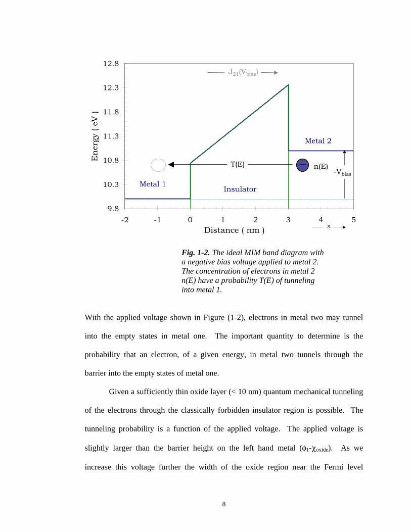
Fig. 1-2. The ideal MIM band diagram witha negative bias voltage applied to metal 2.The concentration of electrons in metal 2n(E) have a probability T(E) of tunnelinginto metal 1.
With the applied voltage shown in Figure (1-2), electrons in metal two may tunnel
into the empty states in metal one. The important quantity to determine is the
probability that an electron, of a given energy, in metal two tunnels through the
barrier into the empty states of metal one.
Given a sufficiently thin oxide layer (< 10 nm) quantum mechanical tunneling
of the electrons through the classically forbidden insulator region is possible. The
tunneling probability is a function of the applied voltage. The applied voltage is
slightly larger than the barrier height on the left hand metal (φ1-χoxide). As we
increase this voltage further the width of the oxide region near the Fermi level

9
decreases. The decrease in tunneling distance results in an increase in tunneling
current. We may also apply a positive voltage to the contact and expect the same
phenomena to take place, this time with carriers tunneling from metal one to metal
two. As before, we expect an increase in carrier current when the tunneling distance
begins to decrease, i.e. voltages above (φ2-χoxide). It is the difference in work
functions of the two metals that leads to an asymmetric I(V) curve. I will present the
precise shape of the I(V) curve and full theory in Section III.
iii. Illumination of MIM Diodes
There are different models applicable to illuminated MIM diodes. The
appropriate model depends upon the specific shape of the MIM diode J(V) curve and
the frequency and intensity of the illumination. Figure (1-3) depicts the different
models and the regions where they are most applicable.

10
Fig. 1-3. The various illuminated MIM diodemodels and their projected range of applicability.Hot-electrons, which may occur without anantenna, are increasingly important at highfrequency.
The specific definition of high and low frequency and high and low photon number
depends upon the I(V) curve for the unilluminated MIM diode. I will define high and
low frequency more clearly in Section V.
If an antenna is used to couple the incident radiation across the oxide of the
device the electric field will induce a voltage across the oxide of the MIM diode. For
low frequencies the device operates as a classical rectifier. The classical regime is
divided into two regions: linear and square-law rectification. When the magnitude of
the oscillating voltage is small, corresponding to a low number of photons, square-
law rectification applies. The MIM diode is not functioning as a switch but rather
����������
��� ������ ���
������
��������� � ��
��������� ���
���������� �����
���
����� ��
����
� ��
���������

11
produces a rectified voltage due to the nonlinearity in the I(V) curve. As the size of
the oscillating voltage increases linear rectification applies. As we will find in
Section IV, for a MIM diode functioning as a rectifier the maximum operating
frequency is limited by the RC time constants.
As the frequencies increase the size of the electromagnetic quanta become
sizeable in comparison to the voltage width of the nonlinearity in the unilluminated
MIM diode J(V) curve and classical rectification theory is no longer appropriate. The
semiclassical theory of photon assisted tunneling, which does not quantize the
electromagnetic radiation, accounts for the quantum size of the electromagnetic field.
This theory limits to the classical theory at low frequencies. If the number of photons
incident decreases or coupling between the radiation and the MIM diode is strong a
full quantum calculation is required. In the full quantum calculation the electric field
of the incident radiation is quantized (quantum electrodynamics).
If an antenna is not used to illuminate the MIM diode, tunneling carriers may
be created by hot-electrons. Each incident photon couples its energy to a single
electron that is excited to a higher energy level. If the excited electron is near the
barrier region and possess the proper momentum it may tunnel through the junction,
producing a current. If the electron relaxes, rather than tunneling through the barrier,
the absorbed quanta will be re-emitted. For low frequencies the probability for the
electron to tunnel through the barrier is low and consequently the device does not
exhibit an optical response. As the photon energies increase, so to does the tunneling
probability. Consequently in Figure (1-3) I have depicted the hot-electron model to

12
be present in all regimes, but with decreasing importance at lower frequencies. I will
present the theory for MIM diodes using hot-electron emission in Section VI.
iv. Thesis Organization
I will begin in Section II by presenting the MIM diodes fabricated through the
course of this thesis work. All of the MIM diodes I fabricated are planer devices
fabricated either with a shadow mask or photolithography. The measured dark
current vs voltage curves will be presented. In Section III I will present the theory of
the MIM diode’s unilluminated I(V) characteristics. Calculations I made on the
specific role of the material selection on the MIM diode operation will presented.
Comparison between the theory and experiment will be presented. In Section IV, I
present the theory of MIM diodes coupled to antenna’s which are illuminated with
low frequency electromagnetic radiation. A PSpice model I developed to simulate
this situation is presented. In Section V I present the quantum theory of photon
assisted tunneling applied to solar energy conversion with MIM diodes to extract
conversion efficiencies. In Section VI I present the hot-electron theory applied to
MIM diodes used for solar energy conversion. In Section VII I present resonant
tunneling concepts which I used to enhance the asymmetry found in the current vs
voltage characteristics of MIM diodes. I conclude in Section VIII with the
ramifications of this work and suggestions for future work.

13
II. EXPERIMENTAL MIM DIODES
In structure MIM diodes are elementary electron devices. Despite this
conceptual simplicity fabricating functional and reliable MIM diodes is challenging.
Even with today’s advanced lithographic technology the majority of MIM diodes
used in practice are of the point contact variety. In this section I present several of the
MIM diodes that I have fabricated through the course of this thesis work. I detail the
fabrication techniques, measurement apparatus, and the measurement results.
i. MIM Diode Fabrication
To fabricate an MIM diode we must consider the substrate, the metals, the
oxide and the patterning technique. I begin this section by exploring each of these
components. I discuss the various methods and materials I tried using and why. A
table of the MIM diodes fabricated is included in Appendix III.
Substrate
I used a variety of substrates to fabricate MIM diodes upon. The first MIM
diodes I fabricated were on microscope slides simply because the slides were
inexpensive and readily available. Additionally, microscope slides would allow for
optical illumination of the MIM diode through the substrate.
Cleanliness of the substrate is crucial. The oxide of a MIM diode is typically
less than 5 nm thick and easily shorted or damaged by particulate contamination. I
cleaned the microscope slides by rinsing them on a spinner at 500 rpm. The specific

14
chemical sequence used was trichloroethylene, acetone, 2-proponal and finally a spin
dry at 6000 rpm. The chemicals were CMOS grade manufactured by JT Baker (JT
Baker, 2001) and dispensed through a squeeze bottle onto the slide for a minimum of
30 seconds each.
I thermally evaporated metal from a tungsten boat onto the microscope slide
and inspected the surface quality under an optical microscope using 5 to 80X
magnification in both reflection and dark-field viewing modes. The evaporated metal
layers on the microscope slide were found to be rough and contained visible particles.
The problem was linked to the inadequate cleaning process. I attempted to reduce the
particle problem by introducing a physical scrub of the microscope slide using Micro
soap in de-ionized water (DI water) prior to the chemical rinse (International, 2001).
The physical scrub was done by hand in an overflow rinse tank using gloves. The
physical scrub visibly reduced the number of particles on the substrate though not to a
satisfactory level. Consequently, an alternative substrate was sought.
I tried using round fused silica flats to fabricate MIM diodes on. The fused
silica flats were expected to have a smoother surface. The ability to illuminate the
MIM diode through the substrate would not be lost. I used the same physical scrub
and degrease procedure used on the microscope slides. The number of visible
particles was reduced further but not to a satisfactory level.
I decided to use silicon as the substrate for MIM diodes. Silicon is a flat
readily available substrate that can be subjected to many proven cleaning solutions.
Silicon’s only disadvantage is that it would not allow for illumination of the MIM
diode through the substrate in the visible spectrum.

15
I used silicon wafers with various crystalline orientation and doping levels. I
grew a wet thermal oxide on the wafers that was at least 1 ��������������� �����
conditions were 1000 oC for 4 hours. The oxide was necessary to electrically isolate
the MIM diode from the silicon substrate.
The wafer, typically three inches in diameter, was subsequently scribed into
one inch squares and cleaned. Everyone questioned about the best method to clean
silicon seemed to have their own favorite recipe or procedure. I investigated and
attempted several of these cleaning procedures; some were successful, some were not.
The cleaning procedure that I eventually found to be the most successful was the
RCA clean (Iscoff, 1993). The RCA clean consists of the following steps:
Oil removal
1) SPM solution (1:1 solution of hydrogen peroxide and sulfuric acid)2) 12 minute soak in SPM3) 12 minute DI water rinse
Organic contaminant and metal removal
1) SC1 solution (5:1:1 solution of DI water, ammonium hydroxide, andhydrogen peroxide)
2) 12 minute soak in SPM at 80 ��3) 12 minute DI water rinse
Oxide removal
1) Dip in 6:1 BOE for 45 seconds2) Rinse in DI water for 25 seconds
Atomic or ionic component removal
1) SC2 solution (6:1:1 solution of DI water, hydrochloric acid, and hydrogenperoxide)
2) 12 minute soak in SC2 at 80 ��3) 12 minute DI water rinse4) Blow dry with nitrogen

16
Any unnecessary step introduced into a cleaning sequence is considered to be
a “dirty” step. As a result, I eventually omitted the buffered oxide etch (BOE) step
from my cleaning sequence. Omitting the BOE is acceptable because I intend to use
the oxide of the silicon for electrical isolation between the MIM diode and the silicon
substrate. In practice I did not find omitting the BOE step to degrade the cleanliness
of the oxidized silicon substrate.
The SC1 and SC2 solutions should be prepared fresh before each clean and
kept well separated from each other to prevent the formation of crystallites
(Campbell, 1996). The DI water in the two tank overflow system was maintained
���������������������������������������������������������� �����������������
in the designated “dirty” tank and the remaining 10 minutes took place in the “clean”
tank.
The wafers were held in a PFA basket manufactured by Entegris (Entegris,
2001) throughout the cleaning process until the final nitrogen dry step. After the final
DI water rinse the wafers were removed using clean metal tweezers and carefully
blown dry. The tweezers were always placed down wind of the nitrogen flow across
the sample with the lower edge of the sample on a cleanroom wipe to absorb the
water that was blown off the edge of the substrate. This substrate and cleaning
procedure proved to provide a clean particle-free substrate.

17
Metals
MIM diodes were fabricated by depositing a base metal layer, oxidizing the
base metal and applying a top contact. The metal deposition for all the MIM diodes I
fabricated was accomplished by evaporation. There are three prerequisites for the
base metal: adhesion to the substrate, a smooth uniform surface, and a suitable native
oxide. I fabricated MIM diodes with base metals made of titanium, aluminum,
chromium, nickel, and niobium. The titanium, aluminum and nickel were 99.99 % or
greater purity purchased from Cerac, Inc (Cerac, 2001). The Cr metal was purchased
from R.D. Mathis (R.D. Mathis, 2001). The niobium depostion was carried out by
ITN Energy Systems using e-beam evaporation.
Obtaining good adhesion of the metal to the substrate turned out to be a
monumental problem in MIM diode fabrication. The lab evaporator, which used a
mechanical roughing pump and an oil diffusion pump (with a liquid nitrogen cold
trap) required a watchful eye. The foreline pressure was kept below < 20 mT when
opening the valve to the diffusion pump and during the evaporation to prevent oil
backstreaming into the bell jar. Oil backstreaming into the bell jar would adversely
affect metal adhesion and purity.
In theory higher evaporation rates produce a higher purity film due to a lower
incorporation of contaminants. However, I found that to produce a smooth metal
surface the evaporation rate had to be kept low, in the range of 0.2 to 0.3 nm/s. For
aluminum, a covered boat was required to prevent splattering of the Al. Chromium
was evaporated from a chromium-coated tungsten rods, while the other metals were
evaporated from tungsten boats.

18
In MIM diodes the base metal forms a native oxide. This native oxide layer
can make contacting the base metal difficult. As a result, contact pads were
eventually incorporated into the MIM design. Initially silver was used to form the
contact pads until I found that the oxygen plasma steps, incorporated into the
photolithography procedure, oxidized the silver. Additionally, the silver would
naturally oxidize over time. Gold proved to be a superior contacting material as it
endured the processing steps the MIM diodes were subjected to and did not oxidize
over time.
Almost two years into the project I found that the metals suddenly no longer
adhered to the oxidized silicon substrate. The adhesion was evaluated using the
“tape-test.” The tape-test is a rudimentary experiment where a piece of tape is
applied to the evaporated metal layer and then removed. The metal is pulled off the
substrate with the tape unless there is good adhesion of the metal to the substrate.
Changes in metal adhesion immediately supports the possibility of oil
backflowing into the bell jar; oil was found on the surface of the bell jar. The
evaporator system was completely dismantled, sandblasted and cleaned with
aluminum wool and 2-propanol. Subsequently the system was “baked out” using
quartz filaments and heating empty boats. The metal adhesion, though improved, was
not satisfactory and a solution to the direct adhesion of silver, gold and aluminum to
silicon dioxide was not found.
As a result, I introduced metal bonding layers to improve adhesion between
the contact pads and the substrate. Initially titanium was used as a bond layer.

19
However, I later discovered that titanium would break up and scatter across the
substrate when subjected to the oxygen plasma and lithography development.
Chromium proved to be the best bonding metal as it readily adheres to silicon
dioxide and is not damaged by oxygen plasma processing. The thickness of the
chromium adhesion layer was typically 100 nm. This is much thicker than required
for a bond layer. The 100 nm thick chromium served a dual purpose as a bond layer
and electrical contact pad. Gold alone is soft and easily scraped away by tungsten
probes during contact. Chromium alone oxidizes and provides an unreliable contact.
By placing gold on top of chromium, the gold prevents the chromium from oxidizing
and the chromium eliminates poor contacting if the tungsten probe scrapes through
the gold.
Although the adhesion of the gold to the SiO2 substrate was ensured by using
a Cr bond layer I was restricted to low temperature processing. The combination of
gold and Cr, when subjected to an elevated temperature (274 oC and greater) would
result in rough mounds forming on the surface as shown in Figure (2-1). This
occurred to lesser degrees as the temperature was decreased.

20
Fig. 2-1. Microscope image of a portion of thecontact pad and base metal on MIM163 (80X). Thesample was heated to 274 oC to oxidize the basemetal. The rough mounds are isolated to the Au/Crportion of the pad.
Despite the damage induced by high temperature oxidation and annealing, the 100 nm
Cr bond layer with a 100 nm of Au provided the most reliable contact. The reason to
subject contact pads to these temperatures is to increase the oxide thickness on the
base metal and remove any excess surface oxygen. Gewinner showed that Cr2O3
produced at room temperature resulted in an excess of oxygen at the surface that
could be removed by a 500 �������!�"Gewinner, 1978). It is unknown what, if any,
effect this surface layer of oxygen has in MIM diodes.
Base Metal(Cr)
Contact Pad(Cr/Au)
Substrate (Si/SiO2)

21
Oxides
The oxide of the MIM diodes were formed by five different techniques:
anodic oxidation, evaporation, thermal, room temperature, and atomic layer
deposition (ALD). The quality of the oxide is crucial to MIM diode performance.
Initial oxides were formed by anodic oxidation of titanium in an attempt to
repeat devices formed by Garret Moddel in 1982. Anodic oxidation is a self-limiting
chemical process where the sample to be oxidized serves as an anode and is
submersed in an electrolyte separated from a non-oxidizing cathode. A potential is
applied between the anode and cathode. The current is limited and eventually drops
to zero as the oxide reaches a thickness that is limited by the magnitude of the applied
voltage (Deeley, 1938). Titanium forms an anodic oxide of 1.5 nm/V (Maissel,
1970).
In anodic oxidation, the chemistry of the oxidation solution is of extreme
importance in order to form a quality oxide and prevent the anode metal from going
into solution rather than oxidizing. If the pH of the electrolyte is incorrect the oxide
may redesolve after formation. Without a proven recipe to go by, I attempted an
electrolyte of 100 ml acetic acid and 900 ml of tap water.
The anode was formed by titanium evaporated on a glass slide that was
approximately 1” � 1” in size and a tungsten rod served as the cathode. The voltage
source was raised slowly to maintain a current less than 200 �#�����!� �� ��!������
reached and the current decreased to less than 3 �#���#!����$�� ������%!�����������
oxide, the oxides were found to be visibly non-uniform. Limiting the current to less
than 60 uA increased the uniformity of the titanium oxide. Uniformity of the titanium

22
oxide was further increased by forming a 2 V oxide in an electrolyte of 50 ml acetic
acid to 100 ml tap water.
Despite the visible improvements in the anodic oxidation attempts the MIM
diodes electrical characteristics were unrepeatable. Most MIMs were shorts.
Investigating the literature for anodic oxidation I found that anodic oxidation is most
suitable for thick oxides (> 10 nm) and often contained ionic current components
(Diesing, 1999). As a result alternative oxide formation techniques were sought.
Further investigations of anodic oxidation of titanium should begin with
alternative electrolytes. Climent has produced TiO2 films suitable for capacitors at
low voltages using non-aqueous solutions of sodium acetate in ethyl glycol (2.97 %)
(Climent, 1993). The aqueous solutions of nitric acid to water (1.79 %) were found to
form nonuniform and poorly adhering oxides. Higher oxidation rates may also be
possible by simultaneous illumination with UV radiation (Kalra, 1994). Additionally,
higher dielectric constants can be obtained by anodic oxidation at elevated
temperatures (Shibata, 1994).
I made several attempts to form the oxide by evaporation of silicon monoxide.
I used thermally evaporated silicon monoxide in a previous project for alignment
layers in ferroelectric and nematic liquid crystal cells and was familiar with the
evaporation procedure (Eliasson, 1999). I evaporated 2 nm and 6 nm thick SiO layers
on a titanium base metal with chromium top contacts to form MIM diodes.
Unfortunately, the evaporated SiO was found to contain pin-holes and resulted in
shorted devices. Attempts to reduce the pinholes in the SiO by moving the substrate
during the evaporation were unsuccessful.

23
Atomic layer deposition was next used to form the oxide layer in MIM diodes.
The atomic layer deposition of Al2O3 was carried out by Jason Klaus and Stephen
Ferro from Steve George’s research group in the chemistry department at the
University of Colorado at Boulder. ALD is a self-limiting chemical deposition
process. Water, transported by nitrogen, is introduced into a tube chamber containing
the sample to be coated. Hydrogen peroxide has also been shown to produce Al2O3
(Fan, 1991). By chemisorption the wafer is fully coated by one molecular layer of
water. The system is then flushed with nitrogen. Trimethylaluminum or TMA,
Al(CH3)3, is next introduced into the chamber using the nitrogen carrier gas. TMA
reacts violently with the water on the surface of the substrate resulting in the
formation of Al2O3. The TMA is then flushed out with nitrogen and the process is
repeated until the desired thickness of Al2O3 is obtained (George, 1995).
Initial ALD films proved to be problematic for several reasons: making
electrical contact to the metal below the ALD film, long range uniformity in oxide
thickness, and large currents in response to applied voltages. The long range non-
uniformity in oxide thickness was verified by ellipsometry. A non-uniformity in
oxide thickness results in a scatter in the current magnitude measured from contact to
contact on a single substrate.
ALD oxide thickness on chromium substrates was measured with a manual
ellipsometer using a wavelength of 632.8 nm at an incident angle of 70 degrees. A Cr
sample with a native Cr2O3 layer was tested prior to the ALD deposition to extract n
and k values for the uncoated substrate. I obtained a composite value for the
Cr/Cr2O3 substrate of n=3.34 and k=2.266 (Tompkins, 1993). Using a nominal value

24
of Al2O3� �!��������������������&&� ���!��!�� � �����vs � trajectory for the single
��!�� ��� '�$��� "���(� �� � ������ � ��� ��� � ��������� ����� �)������!��� �� ��
values.
20 40 60 80� �Degrees�
50
100
150
200
250
300
350
��
seergeD
�
Fig. 2-2. �������������� �������� ���������single film with n=1.77 on a composite Cr/Cr2O3
substrate. The region of the trajectory for a 0 to 10nm thick film is shown in red.
On MIM 12A-12D I measured the following oxide thickness from
ellipsometry. For MIM12A, which had a nominal ALD thickness of 10 nm, I
measured values of 7.7, 7.3, and 7.4 nm across the film. For MIM12B, which had a
nominal ALD thickness of 4 nm, I measured values of 3.1, 3.5, and 4.1 nm across the

25
film. For MIM12C, which had a nominal ALD thickness of 3 nm, I measured values
of 3.7, 4.0, and 3.6 nm. For MIM12D, which had a nominal ALD thickness of 2 nm,
I measured values of 2.9, 2.5, and 2.7 nm. The measurements indicate both a
deviation from the nominal thickness and a deviation across the sample.
The large current magnitudes (90 mA/cm2 at 0.5 volts through a 10 nm thick
oxide) were speculated by Steve George to be due to hydroxyl groups within the
oxide. As a result, several ALD MIM diodes were fabricated using various
temperature anneals to drive out the hydroxyl groups. These experiments were
inconclusive due to the melting temperature of the base metals being lower than the
temperatures required to fully drive out the hydroxyl groups (1000 K). Furthermore,
due to the slow turn-around time that we initially experienced with the ALD films I
began investigating other oxidation methods. I later returned to using ALD oxides
deposited by Jeff Elam from Steve George’s group to form MIM diodes with a dual
insulator layer.
A significant discovery during these initial MIM diode fabrication attempts
using ALD was that the ALD did not adhere fully to the silver metal as it did to
chromium and aluminum. As a result, I was able to use Ag to mask off regions of the
substrate from ALD deposition and solve the problem of contacting to the base metal
below the ALD film.
With semiconductors the best oxides are formed by thermal processes.
Consequently I investigated forming Al2O3 by thermal oxidation of the base metal. I
attempted to repeat the work of Pollack and Morris (Pollack, 1964). Pollack and
Morris formed thermal oxides of aluminum and subsequently MIM diodes that

26
matched theory. Various attempts were made to form MIM diodes in this manner.
The evaporated base aluminum layer was oxidized for up to 54 days at 180 °C both in
oxygen and ambient environments. All devices formed resulted in short circuits.
Subsequently, I attempted to oxidize the aluminum at elevated temperatures in
hopes of forming a thick oxide, at which point I could then reduce the thickness of
subsequent oxides to the desired thickness range by reducing the oxidation
temperature. The oxidation was carried out in a tube furnace at temperatures between
400 and 500 oC for 20 minutes to 2 hours with an oxygen flow of just over 1 cm2/s
parallel to the sample. Lower flow rates in oxygen resulted in a visibly non-
uniformity in the oxides.
After the oxidation, I noticed bubbles on the surface of certain aluminum
samples. The bubbles were isolated to poor adhesion of the aluminum to the
substrate. Using a tape test poor adhesion of the aluminum was confirmed and found
not to occur in the samples with good adhesion. These experiments were carried out
before I routinely used Cr bond layers.
I also noticed other particulates form on the surface of the aluminum after the
oxidation. Close examination of these particulates showed their crystalline nature as
shown in Figure (2-3).

27
Fig. 2-3. An 80 X optical microscope image ofcrystallization in Al2O3 formed by hightemperature oxidation. Note also the bumps(one is circled in the upper left corner), that areformed on the surface of the aluminum oxidesurrounding the crystallized region.
A publication by Wefers and Misra explains that the growth of crystaline
aluminum oxide occurs at temperatures greater than 377 oC. The crystalline
aluminum oxide is coincided by cracking in the amorphous aluminum oxide layer that
is formed at lower temperatures. Consequently, for tunnel quality oxides we should
oxidize at temperatures below 377 oC. Aluminum oxide may be formed in the
presence of water or dry. However, if water is present the concentrations of water,
oxygen, and aluminum must be carefully controlled to prevent the formation of
alumina gels. These gels of aluminum are not the electrical device quality oxides
desired and result in the formation of crystallized “chunks.” (Wefers, 1987)
In parallel with the high temperature oxidation experiments I attempted to
oxidize the aluminum base metal at room temperature. Most MIM diodes formed at
room temperature were short circuits. However, several functional MIM diodes were

28
fabricated. Given this finding, along with the crystallization problems associated
with high temperature aluminum oxidation, I decided the best way to obtain working
MIM diodes was by near room temperature oxidation of the aluminum base metal in a
dry environment.
The environmental control was provided by the bell jar of the evaporator. A
moveable shadow mask was developed which allowed the position of the shadow
mask with respect to the sample to be shifted from outside of the bell jar without
breaking vacuum. Multiple electrodes were installed in the evaporator so that
different metals could be evaporated during a single pump down. An oxygen bottle,
fitted with particulate filters and line dryers, was also connected to the evaporator so
that the bell jar could be back filled with pure dry oxygen during the oxidation stage.
I could then fabricate successful MIM diodes within the bell jar of the evaporator.
Completely controlling the environment is not possible for MIM diodes
formed using photolithography since a portion of the fabrication process occurs
outside of the evacuated bell jar. The lithographic MIM diodes were oxidized either
in an ambient environment or in a separate chamber that had oxygen flowing over the
surface of the samples directly from an oxygen bottle. This continuous oxygen flow
over the sample eliminated the possibility of organic contamination during the
oxidation process.
I also used the native oxide of Cr to form the oxide of MIM diodes. From my
experiences using Cr to form electrical contacts I knew it formed an oxide. Under
thermal oxidation conditions Cr forms Cr2O3 (Fu, 1981). Cr2O3 produces a smooth
oxide, due to ion migration following the Mott-Cabrera Model, up to 600 ���"*���$+

29
1977). Native oxidation of Cr in air produces an oxide approximately 2 nm thick and
moisture has no effect on the oxidation condition at higher temperatures
(Alessandrini, 1972). Cr turned out to produce good MIM diodes.
Patterning
Patterning MIM diodes was accomplished by either direct evaporation
through shadow masks or using photolithography and lift-off or etching techniques.
Patterning MIM diodes using shadow masks has the advantage that it is a cleaner
process since no photoresists or chemical developers are involved. Photolithography
has the advantage that much smaller device areas can be obtained along with the
formation of many more MIM diodes in a single fabrication run.
For MIM diodes fabricated using shadow masks initial devices were made by
evaporating an unpatterned base metal layer over the entire surface of the substrate.
This base metal was then oxidized and top contacts were evaporated through a
shadow mask. These devices required puncturing the native oxide of the base metal
to make electrical contact to the base metal.
For certain metals, chromium in particular, puncturing the native oxide with
the tungsten probes proved to be quite problematic and the resistance between the
probe and the base metal was often large and dependent upon the contact pressure.
Figure (2.4) shows the current vs voltage curve for a single chromium base metal
layer while successively increasing the contacting pressure. A dramatic increase in
current magnitude as the tungsten probe punctures through the oxide is evident.

30
Freshly deposited silver pads, the top dashed trace, have a low resistance on first
contact.
������
������
������
������
������
�����
�����
������
������
�����
������
��� �� ��� �� ��� ��� ��
����������������
���������������
��������� �������
��!�� "�
��
Fig. 2-4. The current vs voltage curve forcontacting the Cr/Cr2O3 base of MIM15 withsuccessive increases in probe contact pressure. Thetop dashed trace is for the first contact of freshlydeposited Ag metal. The current is limited to 40mA.
Furthermore, obtaining a top contact to the device required probing directly on
top of the active junction area of the MIM diode which makes puncturing through the
diode a possibility. The moveable shadow mask system, in addition to controlling the
oxidation environment, allowed electrical contacts to be made away from the active
junction area circled in Figure (2-5).

31
Base Al
TopAg
Fig. 2-5. Microscope image of an MIM diodeformed using the moveable shadow masksystem. The active area of the MIM diode isoutlined in red (Area=0.0014 cm2).
MIM diodes formed using the moveable shadow mask system were quite successful.
The disadvantage of these MIM diodes was that the number of MIM diodes
fabricated for each run was small (49), the junction area was large and only a single
size device was produced for each run.
In order to decrease the junction area size and increase the number of MIM
diodes formed for each fabrication run photolithography was introduced. For my
initial efforts I did not have a dedicated mask for MIM diodes. Using old masks that
had suitably shaped structures I formed MIM diodes by overlapping patterns from
two subsequent photolithography steps by eye shown in Figure (2-6).

32
Fig. 2-6. Optical microscope image of an MIMdiode formed using photolithography. Thejunction area of the MIM diode is indicated bythe red line. (Area=2.3 x 10⁻⁵ cm2)
Without a dedicated mask and proper alignment marks the device area fluctuated and
obtaining a good back contact through the native oxide of the base metal remained
problematic.
I designed a mask, in AutoCAD Light 97 (AutoDesk, 2001), specifically for
MIM diodes. This mask incorporated base contact pads and produced many MIM
diodes of various areas on a single substrate. Ultimately, all lithographic MIM diodes
were fabricated using this mask shown in Figure (2-7).
BaseMetal
Top Metal

33
resistivity & alignment
MIM Device Cell
500 µm
500 µm
wire bond pads
base metal(w/native oxide)
top metal
junction areasrange from :
1µm x 1µm
20 µm x 20 µm
Fig. 2-7. Optical microscope image of an MIMdiode formed by the dedicated MIM diode mask.An individual MIM diode cell (outlined in red)is 500 �������������� ��� �� ��������������2�������2. The region in the lowerleft of the image includes structures foralignment among the three lithography layersand evaluating the resistivities of the metals.
The photolithography process I used was almost exclusively lift-off with
positive photoresist. Although etching would be preferred in many situations because
it allows for thicker metal layers and a cleaner process, it was not always possible due
to the chemical etch attacking one of the previously deposited layers. Lift-off works
by using a negative image of the desired pattern. The resist was removed by the
developer in regions that were exposed to the UV light through the photolithography
mask.

34
The developed openings were cleaned with an oxygen plasma system. I found
that the developer, even with overdevelopment (or even acetone), would completely
remove resist from a wafer once applied. The oxygen plasma was able to remove
residual resist that was left in the developed regions and ensure good metal adhesion.
The oxygen plasma system would also sputter old resist from the electrodes onto the
sample. These resist splatters were approximately 100 nm in diameter. Placing the
samples on clean quartz plates prevented sputtering from the electrodes.
Metal was then evaporated onto the substrate both over the resist and into the
openings. The photoresist is approximately 1 ��������+������� !������ ����������
metal thickness that can be lifted off. Once the evaporation was complete the sample
was submersed in acetone to remove the resist and the overlying metal layer leaving
only the metal that was evaporated into the developed resist openings on the
substrate. If the metal layer was too thick, or the photoresist overdeveloped
ultrasonic cleaning was used to encourage the lift-off.
The specific photolithography steps are outlined below.
1) Spin on HMDS at 6000 rpm for 30 seconds2) Spin on positive resist at 6000 rpm for 30 seconds3) Pre-bake photoresist at 90 ��������,�������
4) Align sample with mask using Karl Suss mask-aligner5) Expose resist to UV light for 27 seconds6) Develop resist for approximately 60 seconds
(4:1.2 of DI water to AZ400K developer)7) Rinse resist in DI water (3 beaker rinse, minimum 30 seconds each)8) Blow dry with nitrogen9) 35 seconds at 200 W at 1 Torr O2 Plasma
This process was repeated for each layer of the MIM diode.

35
ii. MIM Diode Measurements
A table of the MIM diodes fabricated during this thesis work is provided in
Appendix III. I will now describe the equipment used to measure the MIM diodes
and subsequently present a portion of the experimental data measured.
Measurement Equipment
Current vs voltage measurements were made with an HP4145 Semiconductor
Parameter analyzer connected to a probe station (Agilent, 2001). Contact to the MIM
diode was made using two tungsten probes. The resistance of the contact pads to the
MIM diode were low enough that 4-terminal measurements were not used (Dunne,
1990)
Capacitance measurements were made using a Stanford Research SR530 dual
lock-in amplifier (Stanford Research, 2001). A 0.01 V peak 1 MHz sinusoidal
voltage was applied to the sample and provided as a reference to the lock-in. The
sample was housed in a metal enclosure and with the tungsten probes. To calibrate
the system I adjusted the phase of the lock-in, with the probes removed from the
sample, until zero in-phase current was measured. This ensured that the resistance
was infinite when the probes were removed and the circuit is open. The current 90
degrees out of phase was then treated as an offset due to stray capacitance of the
wires and connectors. The probes were brought into contact with the sample and the
resulting current, both in and out of phase was measured using the lock-in amplifier.
The capacitance and resistance was then calculated (Schroder, 1998).

36
This technique for determining the oxide thickness does not include the field
penetration into the electrodes. This field penetration results in a portion of the
applied voltage being dropped across the electrodes and effectively decreasing the
measured capacitance (Simmons, 1965). The field penetration, which has a more
noticeable effect for thinner oxides, would result in an over estimate of the oxide
thickness when extrapolated from C(V) measurements.
Un-illuminated Current vs. Voltage
MIM66 is an example of an MIM diode fabricated entirely within the bell jar
of the evaporator. The substrate was cleaned with the RCA cleaning process. The
base aluminum metal was evaporated at 0.25 to 0.3 nm/s through a shadow mask with
0.005 cm2 holes. After evaporation of the base metal, the bell jar was backfilled with
oxygen to 500 Torr and the sample was oxidized for 2 hours just above room
temperature. The shadow mask was moved and 200 nm of silver was evaporated at
0.15 to 0.5 nm/s to form the top contacts. The resulting MIM diode had a
measured area of 0.0014 cm2 and was shown in Figure (2-5). The current density vs
voltage plot for 10 of the MIM diodes are shown in Figure (2-8).

37
�
� �
��
���
�
�
��
�
�
��� ���� ��� ��� �� ��� ��
����������������
�������������!�#
��
Fig. 2-8. Experimental current density vs voltagemeasurement for 10 of the MIM diodes on MIM66(Al/Al2O3/Ag). The area of the MIM diodes areapproximately 0.0014 cm2.
MIM66 exhibited low scatter in current density magnitude from one MIM diode to
the next.
Capacitance measurements estimated the oxide thickness to be 2.1 nm. The
measured oxide thickness combined with literature values for the Al work function
(4.28 eV), Ag work function (4.26 eV), and electron affinity of the Al2O3 (1.78 eV)
result in simulations which agreed well in magnitude with the measured currents.
MIM84 is an example of a MIM diode fabricated by overlapping lithographic
patterns. The base Nb metal was e-beam evaporated onto an Si/SiO2 substrate. The
Nb was then etched with a niobium etch solution made of 70 % nitric acid, 27 % H2O
and 3 % hydrofluoric acid (Lichtenberger, 1993). Following the etch the samples

38
were cleaned with TCE, acetone, and IPA on a spinner (30 s each) and allowed to rest
in an ambient environment for 3 days to allow the freshly etched edges to oxidize.
Top silver contact pads were formed by a photolithographic lift-off technique. The
active area of the devices is 5.2 � 10-5 cm2. A MIM diode with a similar pattern was
shown in Figure (2-6).
The experimental current vs voltage curves are shown in Figure (2-9).
���
���
� �
���
�
��
�
��
��
��� ���� ��� ��� �� ��� ��
���������������
��������$���%�&�����
���!�#
��
Fig. 2-9. Experimental current density vs voltagecurve for a Nb/Nb oxide/Ag diode MIM84. TheMIM diode’s area is approximately 5.2 � 10-5 cm2.
Several contacts are shown in Figure (2-9) and the scatter is reasonably low. The
barrier between Nb and its native oxide is lower than the barrier between the silver
and the niobium oxide. Consequently, we would expect higher currents under low
negative applied biases.

39
MIM93 is a Nb/Nb oxide/Ag MIM diode that was fabricated with the
dedicated MIM diode mask. In addition an argon plasma was used to mill down the
thickness of the native niobium oxide in hopes of decreasing the resistance of the
MIM diode. I found that the argon milling had three alternative effects. First, I found
the measured currents scaled with edge length as shown in Figure (2-10).
�����
������
������
�����
��� ���� ���� ��� ���� ��� ��� �� ��� ��� ��
���������������
'�������!�(���)����*'�������!#��
�
+
�
���
��+
���
��
�+
��
Fig. 2-10. Experimental current density vs voltagecurve for a Nb/Nb oxide/Ag diode MIM99. Theniobium oxide was subjected to a 10 min argonplasma mill (Forward Power: 112 W, DC voltage: -218 V). The resulting devices did not scale witharea, rather scaled by the length of the edge.
In other words, the current did not scale by the area of the device as would be
expected for MIM diodes but rather scaled by the length of the edge in the MIM
diode. Second, milling resulted in a decrease in currents over MIM84. This is
suspected to be due to sputtering aluminum off of the plasma system electrode which

40
deposit onto the sample and subsequently oxidized to decrease the current. Third, the
soft silver contact pads were visibly roughened due to the argon ion bombardment.
Aluminum MIM diodes formed with the moveable shadow mask were found
to be stable for current vs voltage measurements that were repeated during a single
measurement session. Measurements made a minimum of 24 hours later had a lower
current magnitude than the previous day’s measurement as shown in Figure (2-11).
������
�����
������
���,��
���,��
���,�
��� ���� ��� ��� �� ��� ��
���������������
'��������$���%�&'�����!�#
��
$�&�
Fig. 2-11. The current density vs. voltagemeasurement for MIM81 (Al/Al2O3/Ag). Thedecrease in current magnitude of a single contactover a two month period is shown. The timebetween measurements was a minimum of 24 hours.The diode area is approximately 1.1 � 10-3 cm2.
����

41
If the measurement was repeated 2 hours later the current density did not decrease
substantially. Measurements taken more than 24 hours later did not appear to
decrease substantially more than a measurement made exactly 24 hours later. A plot
of the current density at positive and negative 1 volt vs time is shown in
Figure (2-12).
�����
������
���,��
���,��
���,�
� �� � �� �� � � ��
$�&�-�#.��
�������������!�# ��
,��� �
���� �
Fig. 2-12. Current density for MIM81 at positiveand negative 1.02 V vs the day the measurementwas made.
The substantial decrease in current indicates that the oxide thickness was increasing
with subsequent measurements. MIM81 broke down to a short on the 62nd day.
I suspect this current decrease was the result of current induced oxidation of
the aluminum (Snow, 1996). I speculate that the minimum 24 hour time period was
the time required for the MIM diode to saturate with oxygen and moisture from the
atmosphere and as a result facilitate the current induced oxidation. As the oxide

42
thickness increased the electric field decreased subsequently decreasing the oxide
thickness growth with time.
MIM106 is a small area Al/Al2O3/Ag MIM diode fabricated by
photolithography. The base aluminum was allowed to oxidize by sitting in ambient
conditions for several days. Measurements were made on a single 20 ���� 20 ��
device. In the small area MIM diode I found a saturation time on the order of 10
seconds as opposed to the 24 hours required in the larger area devices. Furthermore,
evidence for ions within the oxide was found in the smaller area devices.
������
������
�����
�����
������
������
�����
������
� � ��� ��� �� �� �
���������������
'��������$���%�&'������!�#
��
�
�
�
Fig. 2-13. MIM106 (Al/Al2O3/Ag) exhibits rapidaging. The numbers and solid arrows indicate themeasurement order and direction. The dashedarrows indicate the direction the current shiftedbetween subsequent measurements. The size of theMIM diode is 20 ��� 20 ���

43
In Figure (2-13) the initial sweep from zero volts to 2.5 V was repeatable with
no decrease in current and no shift in the minimum of the J(V) curve. This indicates
that if ions are responsible for the current lag they are not activated with a positive
bias. This could be explained by saying that the ions are positive and located at the
Al/Al2O3 interface. An argument for negative ions at the Al2O3/Ag interface could
also be applicable though I will assume the former throughout.
The second measurement was a sweep from zero to negative 2.5 volts. A
decrease in current was found to occur in this set of measurements. This current
decrease may be due to shielding of the applied voltage by the activated ions or a
increase in the oxide thickness due to field-induced oxidation. Field-induced
oxidation is expected to be possible for electric fields of 107 V/cm. A –2.5 volt
oxidation potential indicates that the native oxide of the Al was approximately 2.5 nm
thick. Because there was no voltage shift in the J(V) curve minimum from zero in
subsequent measurements the activated ions must redistribute from one sweep to the
next.
The third sweep was from negative to positive voltage. The current
magnitude continued to decrease with subsequent sweeps and a shift in the curve to
the left is evident. This shift is due to ions in the oxide lagging behind the applied
voltage. The magnitude of the shift is proportional to the number of activated ions in
the system.
The fourth sweep was from positive to negative voltage. The current
magnitude no longer decreased in this set of measurements. Furthermore, the
minimum in the J(V) curve is of opposite polarity and equal magnitude to that of the

44
previous scan. Either we have reached saturation in the number of ions that will be
activated, or this sweep direction does not activate ions.
As we see in sweep five from negative to positive voltage, we have simply
reached saturation. The current magnitude continued to decrease slightly, perhaps
due to a small but continued field induced oxidation. The magnitude of the voltage
offset was constant and much like sweep four the current magnitude continued to
decrease only slightly.
The above process was repeated on a different contact. This time however,
after a zero to positive voltage sweep the next measurement was taken from positive
to negative voltage. The shift in the J(V) curve was evident. Again the magnitude of
the offset in the current minimum reached a saturation.
I attempted to limit the aging process by depositing and subsequently
oxidizing through a thin aluminum layer sandwiched between two silver electrodes.
-���������!�+� ��� ���������!!� ������� "���(�� �-���$� �����!���)�������+� ����
unable to produce thin continuous layers of aluminum.
It is possible that hermetically sealing MIM diodes would produce stable
devices. However, due to the aging in these unsealed devices I abandoned aluminum
and its native oxide.
I attempted fabricating several MIM diodes using a nickel base metal. I found
that nickel evaporated from a powder source resulted in a highly resistive metal layer.
.��)������$� ���������!�)!!��� ���!� � ���/0��� ������������ �����))!� ���!��$�
from mV to volts. The problem was the evaporated nickel from our system exhibited
inconsistent conductivity.

45
Subsequent MIM diodes were fabricated from chromium and its native oxide.
Having fought with trying to contact chromium metal in the past I knew it would
easily form a native oxide. Following some initial difficulty forming repeatable
tunnel oxides I constructed a chamber so that the chromium could oxidize under the
continuous flow of oxygen. This technique ensured organic contamination did not
interfere with the oxidation process. Furthermore, my oxides formed from Cr2O3 did
not show signs of aging or ions.
A symmetric MIM diode fabricated from chromium is shown in Figure (2-14).
����
�����
���
�
��
����
���
��� ���� ��� ��� �� ��� ��
�����������
��������$���%�&������!�#
��
����
���
��
���
� �
�
�
��
�
��
���
/����0
� �����!�#
�
1�1
0�
1�1�0�
Fig. 2-14. Cr-Cr2O3-Cr MIM diode (MIM161).The black trace is the MIM current density data.The thick gray trace is a straight line fitted to thezero bias resistance of the diode. The blue trace isthe difference between the MIM diode J(V) curveand the straight line. This illustrate thenonlinearity in the MIM diode. The device size is10 ��� 10 ���

46
MIM161 had about an order of magnitude scatter in the current vs voltage curves
from one MIM diode to the next. The J(V) curve was symmetric for all diodes
measured. The nonlinearity was made evident by plotting the difference between the
current vs voltage curve for the MIM diode from a straight line fitted to the zero bias
resistance of the diode.
Asymmetry may be introduced into the system by using a top electrode made
from a different material. MIM 162 has a top electrode made of palladium. The
current vs voltage measurement for this diode is shown in Figure (2-15).
���
����
��
�
�
���
��
��� ���� ���� ��� ���� ��� ��� �� ��� ��� ��
������������
��������$���%�&������!�#
��
Fig. 2-15. Cr/Cr2O3/Pd MIM diode (162). Thedevice size is 20 ��� 20 ���
The nonlinearity in the Cr-Cr2O3-Pd MIM diode is evident directly from the measured
data. The current density has decreased from the symmetric chromium MIM diode.
A decrease in current density is expected due to the larger barrier between Pd and

47
Cr2O3 as compared to Cr and Cr2O3. The barrier also introduces an asymmetry in the
J(V) curve favoring negative bias voltages.
Even further asymmetry can be obtained by using a magnesium top electrode
as shown in Figure (2-16).
��
��
�
��
�
�
�
�
���� ��� ��� �� ���
��������������
��������$���%�&������!�#
��
��
�+
���
��+
�
+
������!�#�
�����!�#�
Fig. 2-16. Cr/Cr2O3/Mg MIM-L152diode. Thechromium oxide was formed under ambientconditions. The traces are blue for the 20 ��� 20��� ��� ���� � ������ ����� 10 ��� ��� ��and the green for the 5 ��� 5 ��� ��� �������each device are plotted). The diodes broke down atforward applied biases greater than 0.8 V. Thecurrent densities for sample 10B at +/- 0.8 V arelabeled.
The diode made with a magnesium top electrode was found to have relatively little
scatter in the current density from device to device. Additionally, the current scaled
well with area.

48
In Figure (2-16) the diode to diode scatter in MIM152 is negligible for large
area contacts. As the contact size decreased to less then 5 ���� 5 ��� ��� �� �
current density also decreased (the scatter among a given size group remained small).
I speculate that this decrease in current magnitude with decreasing device size is due
to over development in the photolithography process. Overdeveloping the resist
results in rounding of the corners (visible through the microscope). Overlapping
squares with rounded corners reduce the actual size of the MIM diode as compared to
two overlapping squares without any edge rounding as shown in Figure (2-17).
Fig. 2-17. – Effect of overdevelopment on MIM diodearea. Two squares represent the base and top metallayer overlapping to form the MIM diode. The red lineoutlines the MIM diode area formed by perfect squaresoverlapping. With improper development, the edges ofthe square are rounded (shown only on the overlappingcorner). Rounding due to over development results in adiode area that is smaller than what would be producedby two perfect squares of the same size overlapping.
In a lift-off process overdeveloping alone enlarges the squares while rounding the
corners. However, the area I use to calculate area was measured from the width.
Base Metal
Top Metal
Designed Area
Actual AreaReduced byOverdevelop

49
The rounding would occur on devices of all sizes but would have a more
dramatic effect on smaller area devices. To correct for the rounding the area used in
calculating the current density must be decreased which would inturn increase the
current magnitudes.
While fabricating Cr MIM diodes I found that the thickness of chromium
could be increased by elevating the temperatures. Oxidations at temperatures up to
500 �C were carried out. I also found that the oxygen plasma system both increases
the oxide thickness and introduces an asymmetry into the system even when quartz
plates were used to shield the sample from contamination. Using the oxygen plasma
system on the Cr2O3 after formation did not introduce an asymmetry in the J(V)
curve. Consequently, using the oxygen plasma system to clean and oxidize freshly
coated chromium was abandoned.
The MIM diodes fabricated experimentally were all large area (greater than 1
�m � 1 �m) with thick ( > 40 nm) contacts. No optical response was detected from
these diodes. The diodes were fabricated to explore the different material systems
assuming that the performance of the large area devices would be equivalent to the
performance of the small area devices. Of the diodes I fabricated the ones with the
most asymmetry were the Nb/NbOx/Ag and Cr/Cr2O3/Mg diodes. The polarity of the
asymmetry was in the direction expected from theory.
In conclusion, I have fabricated and tested MIM diodes made from oxidized
base metals of Ti, Ni, Cr, Al and Nb and a variety of counter electrodes. Various
substrates, cleaning procedures, patterning methods, and oxidation techniques were
explored. I found the best MIM diode substrate to be an oxidized silicon wafer

50
cleaned with SPM, SC1 and SC2. Thermal evaporation of metals should be carried
out at a low evaporation rate to produce a smooth surface. My best oxides were
formed by oxidizing the base metal in a chamber connected to dry oxygen. Contact
pads made of chromium covered with gold resulted in both good adhesion to the
substrate and good electrical contact. An oxygen plasma clean was required to fully
remove the developed resist. Care must be taken to ensure that the oxygen plasma
process does not contaminate the sample. Aluminum formed a good oxide but the
fabricated devices were not stable over time. Chromium produced good MIM diodes
that were stable over time. Finally, if atomic layer deposition is used either gold or
silver may be used to selectively control the regions where the ALD alumina adheres
to the sample. The comparison between the experimental diode presented and theory
are presented in section III.

51
III. UNILLUMINATED MIM DIODE
In this section I present the theory of MIM diode current density vs voltage
J(V) curve in the absence of illumination. Understanding the dark J(V) curve of MIM
diodes is a prerequisite to effectively optimizing the device structure and calculating
the response to optical illumination. Simulations based on the dark J(V) expressions
help guide the material selection for optimal performance, gauge the quality of the
fabricated devices, calculate the illuminated properties of the device, and the ultimate
goal: predict the solar energy conversion efficiency of MIM diodes.
i. Current Density vs Voltage Theory
In this section I work through the theoretical expression for the current density
vs voltage curve J(V) of the MIM diode in the absence of illumination. The final
expression I develop for the J(V) relation in an MIM diode is equivalent to that found
in Sze (Sze, 1981). However, the explanations provided there make it difficult to
determine what assumptions are used. Furthermore, in the MIM diode literature it is
standard practice to use the analytical approximation of the MIM diode J(V) curve
derived by Simmons (Simmons, 1963) and use the WKB (Wentzel, Kramers,
Brillouin) approximation to the electron tunneling probability (Griffiths, 1995).
These approximations neglect the detailed shape of the insulating barrier.
I limit the number of approximations made and derive the J(V) curve from
first principles. I use the independent electron approximation and develop a one-
dimensional expression for the current density as a function of applied bias voltage. I

52
focus on the MIM diode although in practice this same technique may be easily
extended to the current density calculation for multi-layer metal-insulator tunneling
systems as will be shown in section VII.
The energy band diagram for an MIM diode is presented in Figure (3-1).
��
�� �!
�� �
�� �!
�� �
�"�!
�"�
#" #� � � " ! � �
$�� �� � �� %
& ���� '%
#'(���
) ����
) ���"
*�&% �&%
+"��'(��� %
, �� �����
�
Fig. 3-1. The energy band diagram for an MIMdiode with a negative applied bias voltage.Electrons in metal 2 tunnel through theinsulator and are collected in empty stateswithin metal 1. The result is a current frommetal 1 to metal 2.
The particular material system of the MIM diode in Figure (3-1) is a Cr base metal
(metal 1) with a 3 nm thick native chromium oxide (Cr2O3) and a top metal (metal 2)
made of Pd. Material property values are provided in Appendix II. Due to the large
bandgap of most insulators the valence band is generally omitted in the energy band
diagrams of MIM diodes.

53
In Figure (3-1) a negative bias voltage is applied to metal 2, referenced to
metal 1. The negative bias voltage results in a current from metal 1 to metal 2. The
current flow in the MIM diode is due to electrons emitted from metal 2 that tunnel
through the insulator and are collected in metal 1.
The current density is the product of: the charge carrier density passing
through a plane perpendicular to the conduction direction per second, the carriers
velocity in the direction of conduction υx, and the charge of the carrier -q. In an MIM
diode, the number of carriers contributing to the current is limited by the
concentration of carriers n2(E) available in the emitting electrode, and the probability
they are able to quantum mechanically tunnel through the insulating barrier T(E).
The Fermi distribution functions for metal 1 f1(E) and metal 2 f2(E) where the bias
voltage is applied to metal 2 takes the form
1exp
1)(
1exp
1)( 21
+
+−=
+
−=
kT
qVEEEf
kT
EEEf
biasff
(3.1.1a,b)
where Ef is the Fermi level within the metal, k is the Boltzmann constant, and T is the
absolute temperature.
Mathematically we may express the current from metal 2 to metal 1 in the
MIM diode as a function of voltage as
)()()(2 xx ETEEnqnqJ υυ −=−= (3.1.2)

54
where
)()()( 222 EfEgEn = (3.1.3)
I assume parabolic energy-momentum bands within the electrode and consequently
use the effective mass approximation to calculate the three dimensional density of
states (Pierret, 1989). The density of states has a square root dependence on energy
(Kittel, 1986)
dEEh
mEg
3
23
)2(4)(
π= (3.1.4)
where m is the electron mass, and h is Planck’s constant.
We convert the density of states expression from a function of velocity as in
equation (3.1.2) to a function of kinetic energy by using
υυυ dmdEmE =∴= 221 (3.1.5)
The substitution of equation (3.1.5) into equation (3.1.4) results in a density of states
expression that is a function of carrier velocity.
υυπυ dh
mg 2
3
38)( = (3.1.6)

55
We must make the distinction between the carrier total velocity, as is in
equation (3.1.6), and the component of velocity in the conduction direction x.
Carriers that do not have a component of velocity in the x direction do not contribute
to the current. The distinction in direction is made by transforming from spherical
coordinates, used in the density of states, to Cartesian coordinates. In spherical
coordinates, the density of states is a sphere that when combined with the Fermi
function extends from the origin outward a radial distance equal to the Fermi velocity.
Figure (3-2) pictorially illustrates the density of states sphere in Cartesian
coordinates.
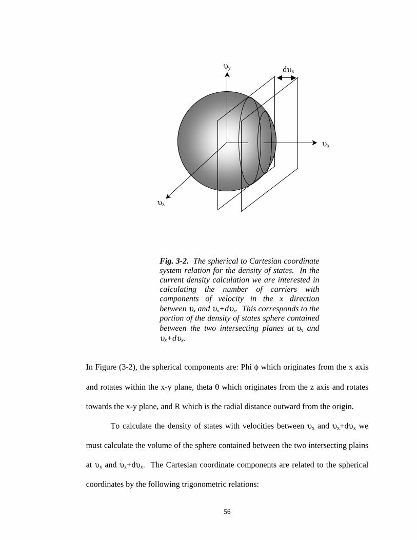
56
Fig. 3-2. The spherical to Cartesian coordinatesystem relation for the density of states. In thecurrent density calculation we are interested incalculating the number of carriers withcomponents of velocity in the x directionbetween υx and υx+dυx. This corresponds to theportion of the density of states sphere containedbetween the two intersecting planes at υx andυx+dυx.
In Figure (3-2), the spherical components are: Phi φ which originates from the x axis
and rotates within the x-y plane, theta θ which originates from the z axis and rotates
towards the x-y plane, and R which is the radial distance outward from the origin.
To calculate the density of states with velocities between υx and υx+dυx we
must calculate the volume of the sphere contained between the two intersecting plains
at υx and υx+dυx. The Cartesian coordinate components are related to the spherical
coordinates by the following trigonometric relations:
υx
υy
υz
dυx

57
dRdzdRdydRdx === θφθ )sin( (3.1.7)
Combining the Cartesian coordinate components together a differential volume is
formed.
drddRdzdydx θφθ )sin(2= (3.1.8)
Integrating theta and phi over their entirety, from -π/2 to +π/2 and 0 to 2π
respectively, we are left with a volume element containing only a radial velocity
dependence.
rrzyx dddddrRdzdydx υπυυυυπ 22 44 =∴= (3.1.9)
Substituting equation (3.1.9) into the velocity dependant density of states we convert
the density of state into Cartesian coordinates.
zyx dddh
mg υυυυ
3
3
2)( = (3.1.10)
We still have components of velocity in the y and z directions that we would
like to fold into the total energy. We do this by converting the dυx and dυy terms
back into spherical coordinates with the use of equation (3.1.8).

58
rryx dddd υθυυυ = (3.1.11)
The differential in theta may then be removed by integrating from 0 to 2π. The
differential in radial velocity is converted into radial (total) energy with the use of
equation (3.1.5).
dEm
dd zy
πυυ 2= (3.1.12)
We combine equation (3.1.10) and equation (3.1.12) and multiply by the Fermi
distribution function f(E) to write the expression for the carrier density as a function
of velocity in the x direction.
∫= xx ddEEfh
mn υπυ )(
4)(
3
2
(3.1.13)
We have the necessary pieces to write the full expression for the current due
to electron tunneling from metal 2 to metal 1 by substituting equation (3.1.13) into
equation (3.1.2).
∫ ∫=→
x
x
E
xx dETdEEfh
qJυ
υπυ )()(4
2312 (3.1.14)

59
As a final step we convert the x directed velocities into x directed energy using
equation (3.1.5).
x
E
x dEdEEfETh
qmJ
x
∫ ∫∞ ∞
→
=
0
232
12 )()(4π
(3.1.15)
The expression J2→1above represents the total current density flowing from metal 2 to
metal 1. Using a similar procedure an expression is derived for the total current due
to electron tunneling from metal 1 to metal 2.
x
E
x dEdEEfETh
qmJ
x
∫ ∫∞ ∞
→
=
0
131
21 )()(4π
(3.1.16)
The total current in an MIM diode is simply a combination of current from metal 2 to
metal 1 and the current from metal 1 to metal 2.
x
E
xDark dEdEEfVEfETh
mqJJVJ
x
∫ ∫∞ ∞
→→
−−=−=
0
1232112 )()()(4
)(π
(3.1.17)
In JDark(V) I have assumed the effective mass in metal 1 is equal to the effective mass
in metal 2. This is the total expression for the un-illuminated, or dark, current density
due to electron tunneling between two nearly free electron metals through an
insulating barrier.

60
Inspecting the dark current density expression we make several observations
about the MIM diode characteristics. First, notice that the current is controlled by the
electron tunneling probability T(Ex) which is a function of the potential barrier
between the metals. As we shall see, the tunneling probability dominates the
expression. Consequently, the precise shape of the barrier is of utmost importance in
MIM diode design. Second, the only temperature dependence of the MIM diode
current density results from the Fermi distribution function. In the next subsection,
we will see that the tunneling probability does not introduce any temperature
dependence. Finally, the density of states in the metal has a linear effect on the
current density magnitude through the electron’s mass within the metal.
ii. Electron Tunneling
The current expression for an MIM diode equation (3.1.17) is complete once
the exact form of the electrons tunneling probability T(Ex) is included. The
probability of an electron tunneling through a barrier from metal 2 to metal 1 may be
calculated using wave mechanics. We will find that the tunneling probability
dominates the shape of the MIM diode J(V) curve.
The MIM diode current expression, equation (3.1.17), assumes a definite
electron energy Ex and as a result we will be completely uncertain of the electron
position. This uncertainty is contained in the plane wave form of the wave function
Ψ.
−−=Ψ
�
tiEikx xexp (3.2.1)

61
For a particle, such as an electron, the uncertainty in position may be reduced by
using a wave packet, or a summation of plane waves.
Boundary conditions must be imposed on the wave function throughout
structure. The first boundary condition is that the magnitude of the wave function
must be continuous. The second boundary condition requires that the derivative of
the wave function, with the exception of delta function potentials, is continuous
(Kroemer, 1994). Additionally, the electron momentum must be conserved in the
tunneling transition.
The probability of finding an electron can be calculated from the wave
function. Because the wave function is a plane wave, with no certainty in absolute
position, we instead look at the relative magnitude of the wave function on each side
of the barrier to determine tunneling probability. Specifically, the tunneling
probability of an electron is defined as the square of the ratio between the magnitude
of the forward traveling portion of the wave function within metal 2 to the magnitude
of the forward traveling portion of the wave function within metal 1.
For simple barriers, such as the square barrier and triangular barrier, the
tunneling probability may be solved analytically (Schiff, 1968). In a real MIM diode
the barrier may not have a simple analytical form and the tunneling probability must
be solved for numerically.
I numerically calculate the tunneling probability using a transfer matrix
approach. For a single interface we can write the spatial wave function on both the
left �l and right �r side of the interface as a summation of a forward and reverse
traveling plane-waves.

62
)exp()exp(
)exp()exp(
xikDxikC
xkiBxkiA
rrr
lll
−+=−+=
ψψ
(3.2.2 a,b)
The time dependence of the wave function, exp(-iExt/�������������������� �� ����
momentum kl,r, as a result of the nearly free electron approximation, is defined as
2
)(2
�
VEqmk
−= (3.2.3)
where �� ��� �������� ������� ��� � � ��� �π and V is the potential energy (Kittel,
1986).
By imposing the boundary conditions that the wave function and its derivative
are continuous at the interface we can derive a transfer matrix between the
components of �l and �r.
( ) ( )
( ) ( )
+−−+
−++−−
=
D
C
k
kkxkki
k
kkxkkik
kkxkki
k
kkxkki
B
A
l
rlrl
l
rlrl
l
rlrl
l
rlrl
2
)()(exp
2
)()(exp2
)()(exp
2
)()(exp
(3.2.4a)
=
D
C
mm
mm
B
A
2221
1211 (3.2.4b)

63
When the effective mass changes across an interface we must multiply the
transfer matrix by the sqrt(kl/kr) to ensure tunneling probabilities do not exceed unity.
Physically this is just conservation of momentum.
We next divide the barrier into a series of infinitesimally small sections and
calculate the transfer matrix for each interface. The transmission of the total barrier
may then be calculated by multiplying together all of the individual transfer matrices
from each interface. From the total transfer matrix we calculate the tunneling
probability of an electron with energy Ex. We assume that the wave function of the
electron within the second metal, after tunneling through the barrier, has no reflected
component and set the value of D in the complete transfer matrix equal to zero. As a
result, the tunneling probability is simply the square of C/A, which is
2
11
1
=
mT (3.2.5)
Inspecting the transfer matrix element m11 we find that the tunneling probability of an
electron is temperature independent.
The transfer matrices contain the spatial form of wave function. Consequently
we may calculate the wave function, or a wave packet, from the transfer matrices.
For example, the Cr/Cr2O3/Pd MIM diode of Figure (3-1) is replotted in Figure (3-3).
I divided the barrier into 600 sections and calculated the transfer matrices for an
electron 2 eV above the Fermi level in the Cr metal (12 eV in the Figure) that is
tunneling from the Cr electrode to the Pd electrode. I then plotted the wave function,
both the real and imaginary components, of the 12 eV electron tunneling from the Cr
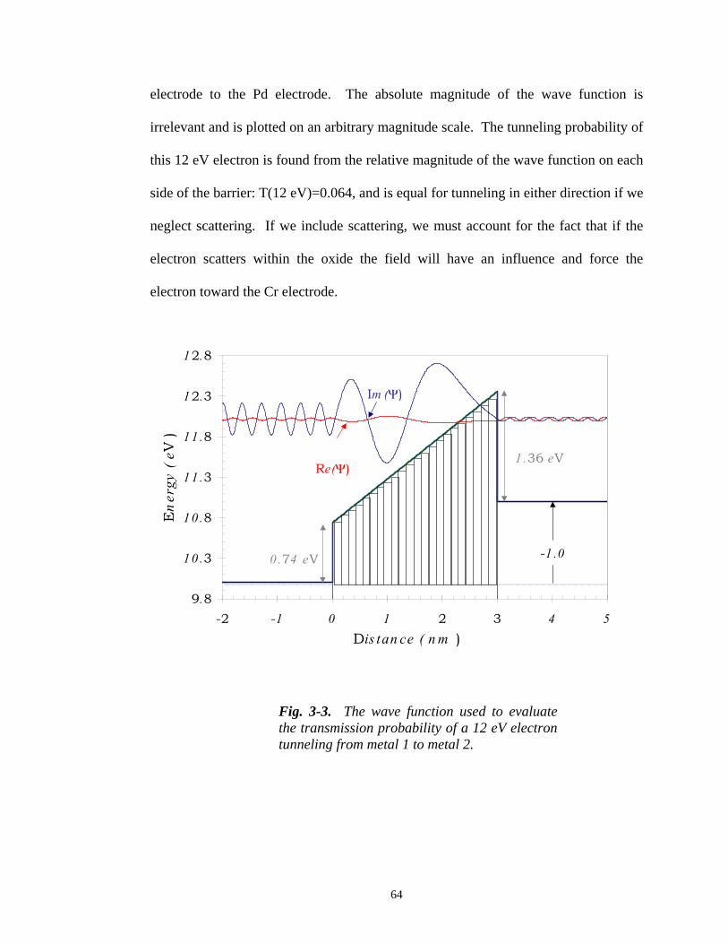
64
electrode to the Pd electrode. The absolute magnitude of the wave function is
irrelevant and is plotted on an arbitrary magnitude scale. The tunneling probability of
this 12 eV electron is found from the relative magnitude of the wave function on each
side of the barrier: T(12 eV)=0.064, and is equal for tunneling in either direction if we
neglect scattering. If we include scattering, we must account for the fact that if the
electron scatters within the oxide the field will have an influence and force the
electron toward the Cr electrode.
��
�� �!
�� �
�� �!
�� �
�"�!
�"�
#" #� � � " ! � �
$�� �� � �� %
& ���� '%
# �
#-�
#��
#"�
#�
��
� �!- '
#� ��
,� �Ψ%
� �.� '
/ �Ψ%
Fig. 3-3. The wave function used to evaluatethe transmission probability of a 12 eV electrontunneling from metal 1 to metal 2.

65
After evaluating the tunneling probability for an electron of a single energy,
we may repeat the process over a span of energies to calculate the electron tunneling
probability as a function of energy. The complete T(E) is plotted in Figure (3-4).
� �&#"�
� �&#�
� �&#�-
� �&#��
� �&#�"
� �&#��
� �&#�
� �&#�-
� �&#��
� �&#�"
� �&0��
� �� �! �� �.
& ���� '%
*�&%
1��
���
234
5 �� �� � �
� � ���"*��" '%6� ��-�
Fig. 3-4. The tunneling probability as afunction of energy for the 3 nm Cr/Cr2O3/PdMIM diode with a negative applied bias of onevolt. The plane wave solution, using transfermatrices, and the WKB solution are shown.
In Figure (3-4) I have included the WKB approximation to the tunneling
probability. The WKB approximation neglects the reflected wave within the barrier
region to produce an analytical function for the T(E) in arbitrary barriers. Notice that
at the Fermi level of metal 2, 11 eV, the WKB approximation results in a
transmission probability value approximately 6 times larger than the plane wave

66
solution. At energies above the Fermi level of metal 2 we find that the difference
between the WKB and plane wave approximation becomes more noticeable in certain
regions. Furthermore, notice that the transmission probability limits to unity in the
WKB approximation for energies greater than the height of the barrier (12.36 eV)
while in the plane wave solution oscillations due to reflections are present even at
energies above the barrier height. The depth of the valleys in the T(E) are affected by
the energy of the electron relative to the top of the barrier.
� �&#��
� �&#��
� �&#�!
� �&#�"
� �&#��
� �&#��
� �&#��
� �&#�
� �&#�.
� �&#�-
� �&#��
� �&#��
� �&#�!
� �&#�"
� �&#��
� �&0��
�� �� �" �! ��
& ���� '%
*�&%
&56�� '
&56� '
&56� '
&50� &50"&50! &50�&5
Fig. 3-5. The tunneling probability as a function ofenergy for a Cr/Cr2O3/Pd MIM diode. The plotshows that the oscillation depth in the T(E)decreases as we decrease the Fermi level in themetal electrodes.
The transfer matrix method for calculating the tunneling probability has
several advantages. First, we are not limited to simple barrier shapes that have

67
analytical solutions. We can numerically calculate both the spatial component of the
wave function and the tunneling probability for any barrier shape. Second, we do not
need to neglect reflections within the barrier as is done in the WKB approximation.
This becomes particularly important if we would like to calculate coherent tunneling
through a multilayer structure containing resonant energy levels. Third, we may
extend this method to calculate the time dynamics of electron tunneling by forming a
wave packet (a summation of plane waves) and calculating its temporal propagation
through the structure at energies both above and below the maximum barrier height.
Simulating wave packets propagating through barriers produces entertaining
movies. On the practical side these movies offer insight into the temporal dynamics
of electrons tunneling through a barrier and through resonant energy levels.
Wavepackets are formed are formed by a summation of planewaves over a range of
electron energies and as a result tend to dampen the oscillations in the T(E) that are
found in the single energy plane wave solution to tunneling.
iii. J(V) For The Cr/Cr2O3/Pd MIM Diode
We are now at the position to numerically calculate the full J(V) curve for an
MIM diode using the current equation (3.1.17) developed in section 3.1 and the
tunneling probability calculations of section 3.2. I assume the Fermi level in both
metals is 10 eV and unity effective mass throughout the structure. The calculated
|J(V)| curve for the Cr/Cr2O3/Pd MIM diode of Figure (3-1) is plotted on a
logarithmic scale in Figure (3-6) where the calculated points are connected by straight
lines.

68
� �&#�-
� �&#��
� �&#��
� �&#�!
� �&#�"
� �&#��
� �&0��
� �&0��
� �&0�"
� �&0�!
� �&0��
� �&0��
� �&0�-
#! #" #� � � " !
'����� �'%
7���� �$ ����7�89��
"%
� ��6!�� �
Fig. 3-6. The simulated current densitymagnitude vs. voltage curve for a Cr/Cr2O3/PdMIM diode with a 3 nm thick oxide. MIM diodeband diagrams have been included at andbetween the various transition points. The banddiagrams within boxes are for a particularapplied voltage, while the other band diagramsare for the indicated regions between.
The oscillations in the current magnitude as a function of voltage evident in
the J(V) curve are a result of the oscillations in the T(E) curve. The physical cause of
these oscillations is quantum mechanical interference due to the reflections of the
tunneling electron within the barrier. In my measured MIM diodes of section II these
oscillations are not evident. The damping of the oscillations in the T(E) result from
fluctuations in oxide thickness, scattering events that break the coherence of the
electron, and the uncertainty in the electron energy.

69
The current vs voltage curve shows several distinct regions that may be
correlated with the shape of the band diagram. The band diagrams of the MIM diode
have been superimposed on the J(V) curve at and between the important transition
regions. With low applied biases (< 0.74 V) of either polarity, direct tunneling of the
electron through the entire width of the oxide limits the current magnitude. Note
however, that under negative applied bias the tunneling is occurring in a direction
opposing the internal electric field while under positive bias tunneling is occurring in
the same direction as the electric field. If a collision were to occur in the tunneling
process the electric field direction would play a role and alter the asymmetry.
However, since I am neglecting scattering, the electric field direction affects only the
manner in which the band shape changes with increasing bias voltage. As we
increase the bias voltage beyond the first transition point, 0.74 V, the negative voltage
band diagram enters into the Fowler-Nordheim tunneling regime where the electron
tunnels through only a fraction of the oxide width (Fowler, 1928). The band under
positive bias reaches a point of zero electric field in the oxide at +0.74 volts and
subsequently continues direct tunneling, only this time in a direction opposing the
electric field direction. As we continue increasing the bias voltage in the positive
direction we reach the second transition point, +1.36 V, where the electrons enter the
Fowler-Nordheim tunneling regime. Under reverse bias, this is not a transition point
and Fowler-Nordheim tunneling continues. Once we apply sufficiently high negative
biases, the 1.36 eV Cr2O3–Pd barrier and the number of electrons available to tunnel
will limit the current magnitude. Under large positive biases the 0.74 eV Cr-Cr2O3
barrier and the number of electrons available to tunnel will limit the current

70
magnitude. Since we have assumed the densities of states and Fermi levels of the two
metals are equal, any differences in the maximum current magnitude in forward and
reverse bias will be due to differences in the barrier heights. Consequently, we find
higher current magnitudes under large positive bias, where the smaller barrier limits
the current, than under large negative bias.
iv. Rectification Reversal
The ratio of the magnitude of the current produced under forward bias to that
produced under reverse bias varies as a function of applied voltage for an asymmetric
MIM diode structure. We define forward bias to be that bias voltage polarity which
produces the higher current for large-magnitude bias voltages. The Cr/Cr2O3/Pd
MIM diode of Figure (3-5) produces a higher magnitude current under high positive
biases than under equivalent negative biases, and consequently is defined as being
forward biased when a positive voltage is applied to the top Pd metal.
Rectification reversal occurs at voltages where the higher current is produced
under reverse bias. For a trapezoidal barrier the polarity of the bias that produces the
higher tunneling probability varies with the magnitude of the applied voltage. Thus,
replotting the data of Figure (3-7) using the absolute value of voltage we clearly see a
rectification reversal that occurs in the J(V) curve of the Cr/Cr2O3/Pd MIM diode.

71
� �&#�-
� �&#��
� �&#��
� �&#�!
� �&#�"
� �&#��
� �&0��
� �&0��
� �&0�"
� �&0�!
� �&0��
� �&0��
� �&0�-
� � �� � � �� " "�� !
7'����� 7�'%
7���� �$ ����7�89��
"%
� ��6!�� �:�� �� �� 4��� '�����
; ����� 4��� '�����
/ �� ������ �� / � ����
Fig. 3-7. Theoretical calculation of theabsolute value of current vs. the absolute valueof voltage for a Cr/Cr2O3/Pd MIM diode.Rectification reversal occurs at approximately1.6 volts.
Rectification reversal may be understood in terms of the electron tunneling
probability. The WKB approximation to the electron tunneling allows us to illustrate
the physical cause of rectification reversal. The WKB approximation is
[ ] ( )20
2/
))((2)()(2exp)(
πh
ExEmxkdxxkET electronc
WKB
−=−= ∫ (3.4.1)
where Ec is the energy of the conduction band within the oxide and Eelectron is the
energy of the tunneling electron (Griffiths,1995). The tunneling probability is a

72
function of the integral of (Ec-Eelectron)1/2 over the fraction of the oxide through which
the electron tunnels, where the energy of the conduction band Ec is greater than the
energy of the tunneling electron Eelectron and subsequently the momentum k(x) is real.
The integral of the (Ec-Eelectron)½ term is responsible for rectification reversal. Direct
tunneling is when the electron must tunnel through the entire width of the potential
barrier, which occurs for low voltages. Fowler-Nordheim tunneling occurs when the
electron tunnels through only a fraction of the oxide’s full width, at higher forward
biases because Ec is less than Eelectron over part of the barrier width. Physically,
rectification reversal is due to the transition between the direct tunneling and the
Fowler-Nordheim tunneling regimes occurring at different magnitudes of bias voltage
in forward and reverse bias, resulting from dissimilar barrier heights at the two metal-
oxide interfaces.
In addition to adjusting the reversal point by changing the barrier heights, we
can also control the voltage location of the reversal point by adjusting the oxide
thickness. I have illustrated this point by calculating the current vs. voltage curve for
the Cr-Cr2O3-Pd MIM diode using various oxide thickness’ and plotted the results in
Figure (3-8).

73
� ��&#�
� ��&#�-
� ��&#��
� ��&#�"
� ��&0��
� ��&0�"
� ��&0��
� ��&0�-
� ��&0�
� ��&0��
� � �� � � �� " "�� !
7'����� 7�'%
7���� �$ ����7�89��
"%
� � ����1�� � � � ��� � ��� �� � � �����
#'
!�� �
!�� �
"�� �
"�� �
� �� �
� �� �
� ��
0'
Fig. 3-8. The simulated current densitymagnitude vs. absolute voltage curves forCr/Cr2O3/Pd MIM diodes with various oxidethicknesses. The figure illustrates the shift inthe rectification reversal point to largervoltages as the oxide is made thinner.
As we decrease the thickness of the oxide layer the reversal point shifts to higher
voltages as the MIM diode conduction becomes dominated by direct tunneling. In
some MIM diode applications it may be possible, by judicious choice of the oxide
thickness, to shift the rectification reversal point out of the diode’s operating range.
I next investigate the effects of changing the barriers in a 3 nm thick
Cr/Cr2O3/Pd MIM diode. Figure (3-9) shows the effects of increasing and decreasing
the work function of the base Cr metal by 0.1 eV.

74
� �&#�-
� �&#��
� �&#��
� �&#�!
� �&#�"
� �&#��
� �&0��
� �&0��
� �&0�"
� �&0�!
� �&0��
� �&0��
� �&0�-
� �&0�.
� � �� � � �� " "�� !
7'����� 7�'%
7���� �$ ����7�89��
"%
<�� ���� !�
7+:� ���$;7
7+:� ���=:7
0'
Fig. 3-9. Current vs voltage for a Cr/Cr2O3/PdMIM diode with a 3 nm thick oxide. The black traceis the standard MIM diode. The red trace has thework function of the Cr decreased by 0.1 eV and inthe blue trace it is increased by 0.1 eV.
Decreasing the work function of the Cr metal increases the current magnitude, which
is expected since we are decreasing the left barrier between the Cr and its native
oxide. This also shifts the reversal point in toward lower voltages.
Figure (3-10) shows the effects of increasing and decreasing the work
function of the top Pd metal by 0.1 eV.

75
� �&#�-
� �&#��
� �&#��
� �&#�!
� �&#�"
� �&#��
� �&0��
� �&0��
� �&0�"
� �&0�!
� �&0��
� �&0��
� �&0�-
� � �� � � �� " "�� !
7'����� 7�'%
7���� �$ ����7�89��
"%
<�� ���� !�� �
7+:� �:�=:7
7+:� �:�$;7
0'
Fig. 3-10. Current vs voltage for a Cr/Cr2O3/PdMIM diode with a 3 nm thick oxide. The black traceis the standard MIM diode. The red trace has thework function of the Pd decreased by 0.1 eV and inthe blue trace it is increased by 0.1 eV.
Decreasing the work function of the Pd metal increases the current magnitude, which
is expected since we are decreasing the right barrier between the Pd and the Cr2O3.
This also shifts the reversal point in toward lower voltages.
Figure (3-11) shows the effects of increasing and decreasing the
electron affinity of the Cr2O3 by 0.1 eV.

76
� �&#�-
� �&#��
� �&#��
� �&#�!
� �&#�"
� �&#��
� �&0��
� �&0��
� �&0�"
� �&0�!
� �&0��
� �&0��
� �&0�-
� �&0�.
� � �� � � �� " "�� !
7'����� 7�'%
7���� �$ ����7�89��
"% <�� ���� !�� �
7+�� �>�=:7
7+�� �>�$;7
0'
Fig. 3-11. Current vs voltage for a Cr/Cr2O3/PdMIM diode with a 3 nm thick oxide. The black traceis the standard MIM diode. The red trace has theelectron affinity of the Cr2O3 decreased by 0.1 eVand in the blue trace it is increased by 0.1 eV.
Increasing the electron affinity of the oxide increases the current magnitude which is
expected, since we are decreasing both barriers in this case. Increasing the electron
affinity of the oxide by 0.1 eV is the same as decreasing the work functions of both
metals by 0.1 eV. This shifts the reversal point in toward lower voltages.
Finally, Figure (3-12) shows the effect of decreasing the electron mass in the
oxide from unity to 0.5.

77
� �&#�-
� �&#��
� �&#��
� �&#�!
� �&#�"
� �&#��
� �&0��
� �&0��
� �&0�"
� �&0�!
� �&0��
� �&0��
� �&0�-
� �&0�.
� � �� � � �� " "�� !
7'����� 7�'%
7���� �$ ����7�89��
"%
<�� ���� !�
7+�� ��6� �� %7
0'
Fig. 3-12. Current vs voltage for a Cr/Cr2O3/PdMIM diode with a 3 nm thick oxide. The black traceis the standard MIM diode. The red trace has theeffective mass of the electron in the oxide decreasedfrom unity to 0.5.
Decreasing the effective mass results in a larger electron tunneling probability.
Consequently, the current magnitude increases with decreasing effective mass and the
reversal point shifts inward to lower voltages.
v. Deviations From The Ideal Barrier
The shape of the energy barrier in an MIM diode was discussed in Section I.
We found that the shape of the barrier was determined by the magnitude of the metal-
insulator barrier height at each interface. The metal-insulator barrier height is ideally
determined by the difference between the work function of the metal and the electron

78
affinity of the insulator. Any deviation in the barrier shape will alter the electron
tunneling probability and subsequently the resultant J(V) curve. In this subsection I
briefly mention the main barrier altering effects and their consequences.
The rectification reversal point in the J(V) curve will be altered if appreciable
field penetration into the electrodes is present. If the field penetration is different in
the two metal electrodes the asymmetry will also be affected (Simmons, 1967). I
have neglected the field penetration in this work.
Image Force
The image force may play a significant role in altering the ideal barrier shape
by effectively lowering the barrier height as seen by a tunneling electron. The image
force is the result of a redistribution of the electrons within the metal due to a point
charge within the barrier. Classically the potential due to the image force can be
written as follows for an MIM diode (Simmons,1963)
( )
−
−+−= ∑
∞
=122
2 1
24 n oxox
ox
oimage dnxdn
dnxqV
εεπ(3.5.1)
where dox is the thickness of the insulator, x is the point particle distance from the
metal-insulator interface, and ε is the permitivity of the insulator. The optical
permitivity is used due to the short time associated with the passage of the electron
from the metal.
The classical form of the image force is often used within the scientific
literature to account for barrier heights extracted from experiments measuring the

79
optical emission of electrons from a metal into vacuum. As we will see, it is
inappropriate to use the classical image force in most un-illuminated (or low
temperature) tunneling experiments.
The more accurate technique for calculating the image force is using quantum
mechanics. The quantum mechanical formulation takes into consideration that the
electron is not a classical point charge within the insulator and that there is a finite
probability of finding the electron within the barrier region.
Quantum mechanically, the image force takes on the following form
(Weinberg, 1978).
∫∫∞
∞− +Ψ
−=−
−Ψ−=
0
220 22
')'(2
),'('
)'(2
),'(dr
rr
trqdr
rr
trqVimage εε
(3.5.2)
In equation (3.4.2) that the magnitude of the image force is a function of the wave
function (a wave packet for an electron). The wave function in turn is a function of
the barrier shape which is altered from the ideal case by the image force.
Consequently the problem must be solved numerically in an iterative self-consistent
fashion.
By approximating the wave function of the electron as a delta function,
Weinberg showed that the quantum mechanical image force is simply a scaling of the
classical image force by the electron tunneling probability. The approximation of the
electron wave packet as a delta function is acceptable if we assume that the wave
packet is not significantly dispersed by the barrier during the tunneling process.

80
The magnitude of the image force varies depending upon the energy of the
electron. We can generalize the effect of the image force as being classical for
carriers well above the conduction band of the insulator where the electron tunneling
probability is near unity and negligible for carriers well below the conduction band of
the insulator. In the intermediate regions, the image force is somewhere between the
classical result and being negligible.
In the simulations including the image force, I use the classical result and
scale it by T(Ex). In these cases it is necessary to iterate to a self-consistent solution
at each energy level, between the T(Ex) value and the barrier height due to the image
force. Including the image force in the un-illuminated current density vs voltage for
the Cr-Cr2O3-Pd MIM diode in Figure (3.5) does not produce a noticeable effect.
This is because in an MIM diode most of the carriers contributing to the current are
located near the Fermi level and the barrier is typically several kT above the Fermi
level, resulting in a relatively small T(Ef) value. Consequently the probability of an
image particle in the barrier region is small and thus so is the image force effect. In
my simulations, unless noted otherwise, I have neglected the image force.
Surface States
Surface states alter the barrier height at the metal-insulator interface (Bardeen,
1947). Surface states are typically due to contamination of the metal or insulator
during fabrication or the chemical structure of the surface. Any deviation in the
barrier heights found experimentally, are most likely due to these surface states and a
clean fabrication process should minimize their effect. Any deviations that result

81
between theory and experiment that can be accounted for by simply adjusting a
barrier height are attributed to surface states.
Pinholes
Pinholes in the oxide will introduce a second conduction mechanism in
parallel with the tunneling current. Pinhole conduction is generally orders of
magnitude larger than the tunneling currents. In addition, pinhole conduction can be
isolated from tunneling conduction by the different temperature dependencies.
Pinhole formation is most likely due to the oxidation process. Any deviations
between theory and experiment that can not be accounted for by tunneling conduction
are attributed to pinholes.
Traps
Traps within the insulator may result in an increased current density in MIM
diodes (Penley, 1962). This is due to the increased tunneling probability through the
electron traps. Trapping time would be expected to limit the response time of the
MIM diode incorporating trap assisted conduction. However, if the traps hold charge
the current will be decreased due to the space-charge (Geppert, 1962).
Effective Mass
The effective mass within the oxide is inseparable from the barrier height in
its effect on the tunneling probability. The effective mass in the metals also plays a
role in the density of states. Because the effective mass of the oxide cannot be

82
isolated from the barrier height I have simply assumed a unity effective mass
throughout the structure. This is a common assumption.
The single value effective mass is only valid near the band edges and will
effect the magnitude and shape of the MIM diode I(V) curve. For electron tunneling
away from the band edge a Franz and Kane type of two-band model is more
appropriate (Gundlach, 1973). In this model two parabolic effective masses, one
from the conduction band and one from the valence band, are combined to form the
effective mass.
Ionic Space Charge
Ionic space charge may be present in many forms and is neglected in our ideal
MIM diode. Interface dipoles, ionic defects, traps, metal ions in the insulator,
electronic space charge, etc., all alter the dominant conduction mechanisms through
the oxide barrier. Positive ions incorporated into the barrier result in an increase in
current (Schmidlin, 1966). Qualitative shape, temperature, and temporal
dependencies separate these mechanisms from ideal tunneling.
Hot-Electron Tunneling Damage
The tunneling of hot electrons through the oxide can result in damage to the
oxide-silicon interface at the receiving electrode (Vogel, 2000). The tunneling hot-
electrons introduce trap states that allow for electron trapping and charging of the
device.

83
vi. Simulation
During the course of this thesis work a significant portion of extra time and
effort was committed to developing simulations to accurately calculate the MIM
diode’s J(V) curve. This simulation, MIMSIM, has been written and subsequently
improved and mutated through many forms.
The fundamental structure of the simulation has remained consistent.
MIMSIM evaluates the MIM diode current density equation (3.1.17) and the T(E).
The numerical calculation is facilitated by a two dimensional grid of fixed step sizes
in energy and distance to define the MIM diode.
The first simulations were calculations made within an Excel 97 spreadsheet
incorporating custom Visual Basic routines (Microsoft, 2001). Three techniques were
used for calculating the T(E) : the WKB approximation, solving the Schröedinger
wave equation by placing the MIM diode in an infinite square well, and the plane
wave transfer matrix approach discussed in section ii. The WKB approximation to
the tunneling probability, as I have shown, neglects the reflections of the electron
wave. Placing the MIM diode within an infinite well resulted in T(E) values that
were strongly dependent on the width of the well used. The complex numbers and
transfer matrices, though producing reliable results, took too long to calculate within
Excel.
A subsequent MIM diode simulation was written in Mathematica 3.0
(Wolfram, 2001). Mathematica offered the capability to easily incorporate flexible
point densities, multilayer structures, and use of its computational engine that was
superior to Excel in handling complex matrices. However, this ease of programming

84
still retained computational overhead and the calculations, though performed with
ease and flexibility, were quite slow.
I next wrote a Matlab 5.3 port of the Mathematica code (Mathworks, 2001).
Matlab, unlike Mathematica, is fully numerical, and I had hoped this would decrease
the computational system overhead and subsequently speed up the simulation.
Unfortunately, Matlab was not significantly faster than Mathematica and further
developments under the Matlab platform were abandoned.
It became clear that in order to remove the overhead inherent with these
software packages it would be necessary to write a freestanding compiled version of
MIMSIM. I chose to write a DOS version using Borland C++ 5.0 (Borland, 2001).
The C version of MIMSIM was written specifically to handle a single insulator MIM
diode, thus losing some of the flexibility I had incorporated into the Mathematica
version.
Many of the mathematical function conveniences provided by Mathematica
and Matlab are not present in the standard C libraries so I needed to write several
mathematical functions. I first wrote code to provide a structure for complex
numbers (Numerical, 1992). I then added routines to perform addition, subtraction,
multiplication, division, absolute values, square roots, exponents, and conjugates of
these complex numbers.
The simulation parameters were stored in two-dimensional dynamic data
structures and thus I wrote routines to both create, clear, print and destroy these
dynamic data structures. In order to calculate transmission matrices, I needed to be
able to calculate using complex matrices. This was a simple extrapolation of the two-

85
dimensional dynamic data structures incorporating the complex data structure as the
matrix elements. In addition to the routines to create, clear, print and destroy these
complex dynamic data structures I wrote a routine to perform matrix multiplication
on them.
Upon completion, the version of the MIMSIM written in C was orders of
magnitude faster than any of the previous incarnations of MIMSIM. However, with
this speed came the requirement that great care must be taken to ensure accurate
evaluation of the integrals. I used box integration with fixed step widths. Given the
nature of the MIM diode current calculation, we are often dealing with numbers on
the order of 10+22 multiplied by numbers on the order of 10-34. This introduces the
potential for numerical errors and care was required to make sure they did not surface
and affect the end result. To a great extent these problems could be controlled by
careful choice in the order that equations were evaluated.
I subsequently made one final port of the code, from DOS to the Windows 98
operating system. This final version of MIMSIM was written with Borland C++
Builder 5.0 in a combination of C and C++. This version was written with the
primary purpose to ease my repeated interactions with MIMSIM via a graphical user
interface. Furthermore, using spreadsheet and database techniques the multilayer
capabilities in Mathematica were reintroduced. The Windows 98 version of
MIMSIM could simulate any multilayer structure of metals and insulators
sandwiched between two metal contacts. The simulation uses the transfer matrix
technique to calculate the T(E) for the MIM diode. Furthermore, it is capable of
including the quantum mechanical image force, calculating the wave-function of an

86
electron in the MIM diode, and the time dependent traversal of a wave packet through
the MIM diode (or multilayer) structure. A screen shot of the MIMSIM 3.0 is shown
in Figure (3-13).
Fig. 3-13. A screenshot of MIMSIM 3.0. Theparameters for the Cr/Cr2O3/Pd MIM diodehave been entered into the spreadsheet on theleft portion of the screen. The central regionare the various user entered simulationparameters. The two yellow bars display thestatus of the calculation during execution andthe output file is displayed on the right side ofthe screen. The various simulation functionsthat may be performed are chosen from the“Simulate” menu.

87
Even with a compiled version of the code, simulation times became
unmanageable as the required point density in energy required to accurately evaluate
the integrals increased. Certain structures, particularly those with resonant tunneling,
require energy steps as small as 10-8 eV to accurately simulate the device. The small
increments of energy resulted in extremely large grids due to the fixed increments of
energy used and consequently dramatically increased the computation time. The
solution was to remove the fixed energy step size and integration. I modified
MIMSIM to dynamically choose a minimum integration range for each applied bias
point and choose as large of energy step size as possible for each increment through
the integration range. Trapezoidal integration techniques were used. The
implementation of dynamic step sizes and integration ranges made structures, which
with previous versions could not be accurately simulated within my lifetime, solvable
overnight.
Additionally, the nested integral of equation (3.1.17), can be reduced to a
single integral if sufficiently high precision numerical evaluations are used. This is
possible since we know that the integral of f1(E)-f2(E-V) from zero to infinity is equal
to V. Consequently, instead of evaluating the integral each time, we can simply keep
a running total of the integral from 0 to Ex and subtract this from the known total V.
If sufficiently accurate numerical evaluations are not used, this method will not
approach zero and an error will be introduced. I found that the computation time
required to evaluate the integral was less than the time required to carry out the
answer to a acceptable number of digits and so I did not implement this trick.

88
vii. Simulation vs Theory
In section II we looked at a few of the MIM diodes I have fabricated and
measured. The comparison between theory and experiment agreed well qualitatively.
The best quantitative fit was with the Al/Al2O3/Ag system in Figure (3-14). Using
literature values for the metal work functions (see Appendix II) and the 2.1 nm oxide
thickness extracted from capacitance measurements, I found the comparison between
the simulation and experimental diode agree quite well in magnitude and curvature
(by adjusting material parameters form their nominal values a precise fit is
attainable).
� �&#�"
� �&#��
� �&0��
� �&0��
� �&0�"
#� �� #� �� � �� � �� � ��
'����� �'%
7���� �$ ����7�
�89��
"%
),)--
<�� � �����
Fig. 3-14. Experimental current density vs voltagecurve for MIM diode 66 made from Al/Al2O3/Ag(solid line) and the theoretical calculation (dashedline).

89
Quantitative fit with the niobium material system was not obtained. Current
magnitudes predicted theoretically, at the maximum applied voltage, were orders of
magnitude larger than the experimental results. Qualitatively the shape of the
experimental data fit the theoretical predictions.
For the chromium MIM diodes, the current magnitudes predicted by theory
were reasonably close to the experimentally obtained values. The curvature of the
I(V) curves did not match the experimental data well. A chromium MIM diode (162)
with a palladium top contact Cr/Cr2O3/Pd is shown in Figure (3-15). The oxide
thickness of MIM162 was estimated to be 1.7 nm from capacitance measurements
assuming a dielectric constant of 10. The asymmetry, larger currents for negative
applied bias, predicted from theory is present in the experimental data.

90
� �&#��
� �&0��
� �&0��
� �&0�"
� �&0�!
#� �- #� �� #� �" � �� � �" � �� � �-
'����� �'%
7���� �$ ����7�89��
"%
Fig. 3-15. Experimental current density vs voltagecurve for MIM diode 162, Cr/Cr2O3/Pd (thick solidline) and the theoretical calculations (circles) for a1.6 nm (upper curve) and 1.7 nm (lower curve)oxide.
Similar agreement was found for the symmetric Cr/Cr2O3/Cr MIM diode 161,
shown in Figure (3-16).

91
� �&0��
� �&0��
� �&0�"
� �&0�!
� �&0��
#� �- #� �� #� �" � �� � �" � �� � �-
'����� �'%
7���� �$ ����7�89��
"%
Fig. 3-16. Experimental current density vs voltagecurve for symmetric chromium Cr/Cr2O3/Cr MIMdiode 161 (thick solid line) and the theoreticalcalculations (circles) for a 1.7 nm (lower curve)and 1.6 nm (upper curve) oxide.
The current vs voltage curve is expected to show no asymmetry between
positive and negative applied biases with current magnitudes approximately an order
of magnitude higher than MIM162 (Cr/Cr2O3/Pd) having a Pd top contact.
In conclusion, a complete presentation of the theoretical dark current vs
voltage curve for an MIM diode was presented. I presented a numerical method to
calculate the electron tunneling probability for an arbitrary shaped barrier, without
neglecting reflections within the barrier. I showed the cause of rectification reversal
and its relation to the various material parameters. I developed several methods to
evaluate the current density vs voltage with a computer. The results of the theoretical

92
calculations, using literature values for the material parameters, were compared to the
experimental diodes. I was able to obtain a range of results that spanned the
experimental results. However, I could not uniquely fit the experiments because (a)
the shape of the curves did not match (b) a perfect fit is of little value since multiple
combinations are possible. To obtain a meaningful perfect fit further experimental
data would be required to confirm the barrier heights, effective mass, and the oxide
thickness.

93
IV. ILLUMINATED MIM DIODE – CLASSICAL THEORY
i. Classical Model
MIM diodes have been used for rectification and mixing of infrared radiation.
The tunneling time of electrons, calculated using wavepackets, have been estimated
to be on the order of 10-16 seconds by several authors and as a result the DC measured
J(V) curve of an MIM diode is the same as that at high frequencies (Faris, 1973). The
estimates of tunneling time calculated from wavepacket propagation, although
frequently used, are questionable (Landauer, 1994). However, experimentally MIM
diodes have been shown to rectify green light (514 nm), indicating the tunneling time
of carriers is not yet a limitation in MIM diodes (Elchinger, 1976). The primary
limitation of the MIM diode response time is the associated RC time constants.
Low frequency illumination of an MIM diode coupled to an antenna can be
understood in terms of electrical engineering circuit theory. Electromagnetic
radiation is incident upon the MIM diode antenna and is subsequently focused across
the insulator of the MIM diode. Treating the incident radiation as a time-varying
potential is acceptable when the MIM diode is much smaller than the wavelength of
the incident light (Wengler, 1992). Furthermore, coupling 100 % of the incident
power from the radiation field to a device smaller than a wavelength of the incident
radiation is possible with proper impedance matching. This remains true at optical
wavelengths (Grober, 1997).

94
Fig. 4-1. Electromagnetic radiation is incidentupon the MIM diode antenna. The antennasubsequently focuses the electric field of thephotons across the MIM diode (located at theoverlap of the antenna). The MIM diode in turnrectifies the electric field to provide power tothe load.
The device shown in Figure (4-1) may be reduced to a classical circuit model
using a sinusoidal voltage source, representing the incident electromagnetic field, a
series resistance representing the antenna impedance, followed by the MIM diode
connected to the load. The MIM diode is modeled as a voltage-dependent resistance
in parallel with a geometric capacitance. This circuit model is an approximation
because, at these frequencies, each of the elements is distributed, not lumped as
shown in the circuit model.
Load
MIM Diode
Antenna
ElectromagneticRadiationV cos(���

95
Fig. 4-2. The classical circuit model of an MIMdiode coupled to the incident radiation throughan antenna. The nonlinearity of the diode ismodeled with the voltage-dependent resistanceRMIM(V). The rectified output voltage appearsacross the load resistor RL. This simplifiedcircuit model neglects the additionalinductance(s), capacitance(s) and resistance(s)that may be associated with the metal andtransmission lines.
The basic circuit model of Figure (4-2) does not include the extra inductance(s),
capacitance(s) and resistance(s) that may be associated with the metal leads to the
antenna, MIM diode, substrate, and the load.
The complex conductivity associated of the metal may be calculated from the
using the Drude model (Ashcroft, 1976).
( ))(
1
1 ωρτωσωσ =
−=
jDC
(4.1.1)
By separating the complex conductivity of equation (4.1.1) into a real and imaginary
portion the capacitance of the metal may be extracted from the imaginary impedance;
where the impedance of a capacitor is equal to the inverse of the capacitance times
Vin cos (���
RA
RLRMIM(V) CMIM
MIM

96
the radial frequency. In Figure (4-3) I evaluate the imaginary impedance and
��������������������� ����������� �������� �������������������������
DC conductivity �DC value of 4.08 � 105 ������ �� � �� ����� � � � � 10-15
seconds.
������
������
������
������
������ ������ ������ ����� ����� ������
� ���������������
����������������
�����
������
������
������
������
������
������
�����
������
�����
�����
!"#"�$%"
����������
&����
!"#"�$%"���
�!
�����
Fig. 4-3. Capacitance and associated impedanceas a function of frequency for aluminum calculatedusing the Drude model.
If we assume that the relevant propagation distance is a quarter of the wavelength we
find that for 500 nm light the capacitive impedance is approximately 25 � 10-21 ohms.
A more important factor at high frequency will be the increase in the
resistance of the metal as a function of frequency due to the decreasing skin depth
(����� ������ ��� � �� ���� �� ����� � ��� !� �"������ �� ����� � ��� �
conductivity �DC and the dc permeability �DC.

97
DCDCf µσπδ 1= (4.1.2)
In Figure (4-4) I have calculated the sheet resistance of aluminum using a DC
permeability value of 4�� 10-7 H/m.
������
������
������
������
������ ������ ������ ����� ����� ������
� ���������������
'����������&���" ���
������
������
������
�����
������
()$��*�#%��������
��
()$��*�#%�
(���%�'��$�%"��� �����
Fig. 4-4. Sheet resistance and skin depth ofaluminum as a function of frequency.
In the green part of the spectrum, we find that the skin depth decrease to 3.4 nm with
a sheet resistance of 7 ohms/square. Consequently, the impedance of the metal
should be taken into consideration for both the antenna and transmission line design.

98
There is a further concern in assuming the solar radiation is coherent across
the MIM diode and that a single sinusoidal source is an appropriate model. The
radius of coherence for the sun may be estimated from the following relation (Saleh,
1991).
⋅
=
source
source
coherence
D
RR
cot2
22.1λ
(4.1.3)
where Rcoherence is the radius of coherence, Rsource is the radius of the source, and
Dsource is the distance from the source. Using nominal values for the radius of the sun
(695950 km) and the distance from the sun (1.6 million km) we find that the radius of
coherence across the spectrum is approximately 1.5 wavelengths. Consequently,
using a single sinusoidal source for a single MIM diode is appropriate. However, if
an array of MIM diodes is used, it is unlikely that the sun will be coherent to all MIM
diodes across the array.
Classical rectification may occur in two different manners: linear and square-
law (Torrey, 1964). The dominant mechanism depends on the explicit shape of the
MIM diode J(V) curve in relation to the magnitude of the oscillating voltage imposed
across the diode. Linear rectification is a large signal model while square-law
detection is a small signal model. In linear rectification we rely on the diode
switching between highly resistive and highly conductive states. In square law
detection the 2nd order derivatives (and higher 4th, 6th, etc.,) produce a rectified
voltage across the MIM diode when only a small oscillation is being induced across
the diode by the incident radiation.

99
ii. Square-Law Rectification
Sanchez developed an analytical small signal model for MIM diodes that
rectify by square law detection (Sanchez, 1974). The model utilizes a circuit similar
to the one in Figure (4-2). The responsivity of the MIM diode is used to determine
the magnitude of the rectified current produced.
Responsivity is calculated from a second order Taylor series approximation to
the MIM diode J(V) curve (Torrey, 1964).
...!3
)(
!2
)(
!1
)()()( 32 +
′′′+
′′+
′+=+ s
ops
ops
opopsop V
VIV
VIV
VIVIVVI (4.2.1)
The differential resistance of the MIM diode at the operating point is equal to the
inverse of the first derivative of current with respect to voltage evaluated at the
operating point. Retaining only the terms through second order in equation (4.2.1)
the voltage out of the MIM diode, without applied bias, may be evaluated using
Ohm’s law.
′′
+′′
= 2
2
1ssMIM V
IVI
IV (4.2.2)
Consequently, the responsivity will be limited to regimes where the second order
Taylor series expansion adequately models the MIM diode J(V) curve.
The small signal voltage induced upon the diode by the incident
electromagnetic energy has the form Vph�cos(����#���������������������$������

100
into equation (4.2.2) to find the rectified voltage, and then through Ohm’s law, the
rectified current.
)(cos2
22 tVI
I phMIM ω′′
= (4.2.3)
The power absorbed in the MIM diode is equal to
IVP MIMMIM ′= 2 (4.2.4)
The responsivity of the MIM diode is defined as the current produced per watt of
power absorbed which may be obtained from the ratio of equation (4.2.3) to (4.2.4).
opVVI
IV
=′′′
=ℜ2
1)( (4.2.5)
In the quantum limit responsivity times the photon energy is equal to the quantum
efficiency.
Sanchez uses the circuit model of Figure (4-2) (neglecting the load resistor)
and assumes that the MIM diode resistance RMIM(V) may be reduced to a single
resistance value about a zero applied bias operating point. This simplifies the model
and allows voltage across the MIM diode to be calculated by voltage division
between the MIM diode and the antenna impedance.

101
Using the MIM diode responsivity the rectified current produced may be
calculated and subsequently the rectified power at the diode. The power conversion
efficiency of the diode is calculated from the rectified power out divided by the
incident power.
( )( )( )
++
+
ℜ=22
2
3
20
121
2
A
MIMMIMA
A
MIM
A
MIM
MAX
R
RCR
R
R
R
R
V
ω
η (4.2.6)
We may make several observations on the conversion efficiency by means of
square-law detection. First, in the limit that RA·CMIM is sufficiently small compared
to the excitation frequency, equation (4.2.6) reduces to a polynomial equation in
terms of the ratio of RMIM to RA. The efficiency is then maximized by setting RMIM =
RA. Then the efficiency is limited by the value of responsivity and the maximum
voltage that may be sustained across the MIM diode without breakdown (VMAX). The
limitations of the approximations are evident because the efficiency increases without
bounds as we increase the responsivity and VMAX.
Physically, in the quantum limit the responsivity has a maximum value of
1/Eph where Eph is the photon energy in electron volts. The maximum voltage VMAX
has an upper limit that depends on the magnitude of electric field that the oxide can
support prior to breakdown.
%��������&'&�������������!�(�����������)����������������
a frequency of 6 � 1013 Hz. The maximum value of responsivity is approximately 4

102
A/W. I will assume that the antenna resistance is equal to the impedance of free
������*++��,���������&'&���)���������-���!�������������)����������
a thin oxide. I will assume the oxide is 1.5 nm thick, has a relative dielectric constant
of 10 and can support a constant electric field of 106 V/cm. The capacitance of the
diode may then be evaluated as 5.9 � 10-6 F/cm2. I will assume that the zero bias
����������� ��������*++�)�������$������..��� 100 nm in size which
corresponds to a zero bias resistance of 3.77 � 10-8�/��2. We may then calculate
the efficiency from equation (4.2.6) as a function of the MIM diode area, or
equivalently the edge length of a square MIM diode, shown in Figure (4-5).
1.E-05
1.E-04
1.E-03
1.E-02
1.E-01
1.E+00
1.E+01
1.E-02 1.E-01 1.E+00 1.E+01 1.E+02 1.E+03 1.E+04
Edge Length (nm)
Eff
icie
ncy
(%
)
Fig. 4-5. MIM diode efficiency, rectified powerout divided by incident power, as a function ofthe diode size.

103
This diode exhibits a peak efficiency of 1.4 % when the diode size is 11 nm � 11 nm.
The peak in efficiency is a direct result of the impedence matching between the MIM
diode and the antenna. A 11 nm � 11 nm diode has a capacitance is 7.1 � 10-18 F
)�������������� ������������� *+��� �������������� ������ ��*��0 �
which may be ignored when in parallel with the smaller capacitor impedence.
' ������������)�������� �����������������������ACMIM were much
less than 1, then the peak in efficiency would reach 60 % with a diode area of 100 nm
� 100 nm, where the antenna resistance is equal to the diode resistance.
Consequently, to obtain high efficiency at high frequencies, we must make the
geometric capacitance of the MIM diode as small as possible, as shown in Figure (4-
6).

104
�
��
��
��
�
�
��
�
������ ������ ����� ������ ����� �����
!+,+������
�--$�$�������.�
Fig. 4-6. MIM diode efficiency as a function ofthe diode’s geometric capacitance. Maximumefficiency is obtained with small MIM diodecapacitance.
The geometric capacitance of the diode may be reduced by decreasing the
dielectric constant of the oxide, increasing the oxide thickness, or decreasing the
device area. The capacitance of the MIM diode decreases linearly with increasing
oxide thickness. Unfortunately, the oxide thickness effects both the resistance and
capacitance of the MIM diode and the current decreases in a highly nonlinearly
fashion with increasing oxide thickness. Subsequently in MIM diode design we
decrease the geometric capacitance of the MIM diode by decreasing the area.
Changes in area alter both the resistance and the capacitance of the MIM diode
linearly.

105
Figure (4-7) shows the calculation of the required MIM diode size (edge
length of a square diode) as a function of wavelength for various oxide thicknesses.
In performing the calculation I have assumed the MIM diode resistance is equal to
*++���������������������������� ����"������(�
���
���
����
�����
������
������ ������ ����� ������ ����� ����� ������
/"0�1��2%���������
($3��4��2%����������
�����
������
�����
������
�����
������
�����
�����
����
�����
Fig. 4-7. The required MIM diode size (sidelength) as a function of wavelength for variousoxide thicknesses. The resistance is assumed to�������������������� ����������������
the RC time constant of the diode times theradial frequency is equal to 1 (the period of thephoton oscillation T divided by the RC timeconstant is equal to 2�).
The RC time constant of the diode is dictated by the size of the MIM diode.
����%������������ �� �������� ��������� ����������$��!�0�)���� ��
����$��������%�1��#� ������ ������������ �����������������(��� 5
T/x = 2� (�RC=1)epsr = 4.5R = 377 �

106
nm diode is required. However, if a lower resistance diode is used this size will
increase.
The resistance of the diode may be decreased substantially by decreasing the
oxide thickness or tailoring the barrier heights. Tailoring the barrier heights does not
change the MIM diode capacitance.
Despite the limitations of the model it teaches that if we effectively
impedance-match the MIM diode to the antenna, Figure (4-3), minimize the
capacitance, Figure (4-4), and maximize the responsivity, Equation (4.2.2), high
efficiency may be obtained. If the magnitude of the voltage imposed upon the MIM
diode become large enough that a second order Taylor series expansion of the I(V)
curve no longer accurately represents the MIM diode I(V) curve we can no longer use
this model. Numerical methods, such as the PSpice model used for linear
rectification, must be used.
iii. Linear Rectification
In linear rectification the magnitude of the voltage oscillation across the MIM
diode is large and the diode functions as a switch. The classical responsivity and
small signal model developed by Sanchez are no longer valid due to the magnitude of
the voltage swing across the MIM diode.
An ideal switching diode has an infinite reverse bias resistance and zero
forward bias resistance. During the positive swing of the sinusoidal input, the diode
is reverse biased and all of the power provided by the input source is dissipated in the

107
load and antenna resistance since RMIM >> RL. At low frequencies, the maximum
power transfer to the load is 50 % when the antenna is matched to the load RA=RL.
At high frequency the capacitance of the MIM diode is important. A capacitor
has an impedance of Zc1���20� 3%MIM). Consequently, we must make CMIM small
such that its impedance Zc is much greater than RL (RA) to prevent stealing power
away from the load. This impedance requirement is met by the statement at the
beginning of this section and in most MIM literature: that RA·CMIM must be
sufficiently small to keep up with the incident radiation, or RA·CMIM is much smaller
than the period of the input oscillation (where RA=RL).
During the negative voltage swing of the sinusoidal input the diode is forward
biased and produces a short circuit across the load since RMIM << RL. Consequently,
the power is dissipated in the antenna resistance. Furthermore, any attempt of charge
storage by means of a capacitor will be ineffective due to the low diode resistance and
subsequent low RC time constant path to ground. This means that although we can
rectify the electromagnetic radiation, we are unable to remove the ripple and truly
convert it to a DC signal with a capacitor. Rather, we must detect the average signal.
In standard rectifiers the load is placed in series with the diode. The RC time
constant of the diode RMIM�%MIM must be kept small so that the diode may keep up
with the incident radiation. In this series configuration a capacitor in parallel with the
load is capable of removing the ripple in the rectified signal.

108
iv. PSpice Model
Accurate modeling of a MIM diode in a large signal circuit requires use of the
I(V) curve at more than a single operating point. The PSpice model allows the
diode’s entire I(V) curve to be taken into consideration and thus also includes
rectification reversal and self-bias effects. The PSpice model is not based on the
device physics of MIM diodes, but instead replicates a user provided I(V) curve. This
allows any electron device I(V) curve to be imported into PSpice and simulated in
any electrical circuit.
The MIM diode I(V) curve is modeled with the use of three circuits: the main
circuit and two isolated subcircuits. The main circuit is shown in Figure (4-8). This
circuit represents the MIM diode and is connected to any circuit via nodes 20 and 30
(the two terminals of the diode). The voltage-controlled current source GMIMI(V101),
where V101 is the voltage at node 101, in conjunction with the two subcircuits
produces a current that is a function of the voltage across the MIM diode (between
nodes 20 and 30). CMIM is the geometric capacitance of the MIM diode.

109
Fig. 4-8. The main metal-insulator-metal diodesubcircuit. GMIMI is a voltage dependentcurrent source. The current produced is afunction of the diode area and the voltage atnode 101 in Figure (4-9).
The first isolated subcircuit is shown in Figure (4-9). This subcircuit produces
a voltage at node 101 which in-turn controls GMIMI(V101) in the main MIM diode
circuit. This circuit must be included in the PSpice net list along with the main circuit
of Figure (4-8), however, this circuit is isolated and node 101 must not be common
with any other portion of the large signal circuit. The voltage at node 101 is produced
by the voltage-dependent-current-source GMIMJ(V100) forcing a current through the
series resistor. GMIMJ uses the PSpice table function to hold the MIM diode I(V)
curve data. The 1 ohm series resistor functions as a multiplier to the current data in
the I(V) table. To reproduce the table data without any scaling, the resistor value is
set to 1 ohm. As a result, the voltage at node 101 is equal to the current produced by
GMIMJ(V100). A change in the scaling factor physically represents a change in the
area of the diode.
����
���������
� �

110
Fig. 4-9. The first isolated subcircuit containingthe table of user provided current vs voltagedata. GMIMJ is a voltage dependent currentsource. The current is dependent on the voltageat node 100 in the subcircuit of Figure (4-10).The current vs. voltage data is held in a PSpicetable.
The second isolated subcircuit is shown in Figure (4-10) The role of this
circuit is to replicate the voltage across the MIM diode (nodes 20 and 30) and in turn
produce a voltage a node 100 that controls GMIMJ(V100). This subcircuit must be
included in the PSpice net list, however, may not have node 100 in common with any
part of the large signal circuit. The voltage-dependent-voltage-source EMIMV(V20-
V30), replicates the voltage across the main MIM diode circuit (between nodes 20
and 30). The 1 megohm resistor is only used to complete the subcircuit.
The combination of the main MIM diode circuit and the two isolated
subcircuits allow any theoretically, experimentally or hypothetically provided current
vs voltage data to be replicated within PSpice.
���� ������
��

111
Fig. 4-10. The second isolated subcircuitreplicates the voltage across the MIM diode.EMIMV is a voltage dependent voltage source.The voltage produced is equal to the voltageacross the MIM diode (the voltage differencebetween nodes 20 and 30 from Figure (4-8)).
A series rectifier circuit consists of an ac input voltage source with a series
resistance to represent the input electromagnetic radiation coupled through an antenna
to the MIM diode, placed in series with the MIM diode model of Figure (4-8). A
standard half-wave rectifier circuit has the load impedance in series with the diode.
For the antenna coupled MIM diode the load impedance must be placed in parallel
with the MIM diode so the electromagnetic field is applied across the oxide. With a
parallel load we are able to rectify the electromagnetic radiation but we are unable to
convert the rectified signal into a true DC signal by means of a capacitor. This is
because a sufficiently large capacitor, to remove the ripple in the rectified signal,
would introduce low resistance path around the load and MIM diode.
The frequency of the input source was chosen at a frequency of 6 x 10¹³ Hz
��1(����������� �������������$�������)�����45�����������������������
in PSpice is 10-21 s). Generally, the solar conversion device operates at much higher
���������������
�

112
frequencies. In linear rectification the MIM diode operates as a switch and we want
the load impedance equal to the antenna impedance for maximum power transfer
during the diode forward bias cycle. We have set both the antenna and load
������������������*++��
The dc voltage VDC across the MIM diode and load resistor and power
conversion efficiency η of the rectifier are then calculated as a function of input
voltage. The power conversion efficiency η is defined from equation (4.4.1-4.4.4).
∫+
∂=Tt
t
INININ ttItVT
P )()(1
(4.4.1)
∫∫++
∂=∂=Tt
t
LOADDC
Tt
t
LOADDC ttIT
IttVT
V )(1
)(1
(4.4.2a,b)
DCDCDC IVP = (4.4.3)
IN
DC
P
P=η (4.4.4)
where PDC is the average output power of the rectifier and Pin is the ac input power.
The average output voltage and current are calculated by integration over an integral
number of periods T.
The theoretical current vs voltage curve for a MIM diode having a left barrier
height of 0.3 eV, a right barrier height of 2.75 eV, and an oxide thickness of 3.0 nm
was simulated.

113
������
�����
������
������
�����
�����
������
� � � � �
56�1%"2�5����6�
5!� ��%�*���$%�5���7&��
���
�6
�6
1010
107
104
101
10-2
10-5
10-8
'��%$-$�"%$���'�0� �"1
Fig. 4-11. Theoretical room temperaturecurrent density vs voltage curve for a metal-insulator-metal diode with a left barrier of 0.3eV, an oxide thickness of 3 nm, and a rightbarrier of 2.75 eV. The solid trace is calculatedusing the WKB approximation to the electrontunneling probability and the dashed trace usesthe numerical plane wave solution. The basemetal is grounded and the voltage is applied tothe top metal.
The diode J(V) data from Figure (4-11) was subsequently used with the PSpice MIM
diode model.
I first used PSpice to simulate the MIM diode of Figure (4-11) within a
standard series rectifier. In the series rectifier the limiting RC constant of the circuit
is the resistance of the MIM diode times the capacitance of the MIM diode. I have set

114
the capacitance equal to zero in the series circuit simulation because the resistance of
the MIM diode increases to large values for low applied biases and would limit the
upper frequency of operation. When the MIM diode is in series with the load
resistance the conversion efficiency and voltage across the load vary as a function
input voltage magnitude. Furthermore, the voltage across the load switches polarity
and the conversion efficiency drops as we pass through the reversal point of the MIM
diode. The efficiency calculation results are plotted Figure (4-12).

115
1.E-08
1.E-06
1.E-04
1.E-02
1.E+00
1.E+02
1 2 3 4 5 6
Input Voltage ( V )
| DC
Out
put P
ower
/ A
C I
nput
Pow
er |
(%
)
1.E-09
1.E-07
1.E-05
1.E-03
1.E-01
1.E+01
efficiencyoutput voltage
| Output V
oltage | ( V )
102
10-2
10-4
10-6
10-8
101
100
10-1
10-2
10-4
10-6
10-8
Fig. 4-12. Power conversion efficiency (ac-to-dc) and rectified voltage output as a function ofpeak input voltage for a series rectifier circuitusing the metal-insulator-metal diode of Figure(4-11). The WKB approximation to the electrontunneling probability is used in the MIM diodeJ(V) calculation and the diode capacitance isneglected. The output voltage is positive to theright and negative to the left of the dip.
The polarity switch in rectified output voltage from the rectifier and the decrease in
efficiency due to rectification reversal are clearly evident at the dip present in the
logarithmic plot. The dc voltage across the load is positive to the right of this dip and
negative to the left.
When the load is placed in parallel with the MIM diode, as we would find in a
solar energy harvesting situation depicted in Figure (4-1), the voltage across the MIM
diode and load is the same. The resistance of the MIM diode is a function of the

116
voltage applied across the diode. As we sweep the input voltage to sufficiently high
values, the MIM diode has a lower value of resistance than the load in both polarities
and shorts out the load. A low resistance current path around the load is introduced
through the MIM diode. With very low input voltages the resistance of the MIM
diode is greater than the load under both forward and reverse biases. Consequently
the high resistance MIM diode in parallel with the load does not affect the current
through the load. Only over a small range of input voltages, where the diode
resistance is larger than the load resistance for a bias of one polarity and smaller for
the opposite polarity, does the MIM diode function as a switch. Consequently,
sweeping the input voltage is not an effective method to detect the reversal when the
diode is in parallel with the load. To illustrate the reversal phenomena in the parallel
configuration I instead fix the input voltage to 5 volts and change the area of the MIM
diode. By changing the area, the resistance of the MIM diode may be shifted with
respect to the resistance of the load and therefore rectification reversal may be
observed.
In the parallel rectifier the dominant RC time constant is the resistance of the
antenna (assumed to be equal to the load) and the capacitance of the MIM diode. The
capacitance of the MIM diode is a function of area. However, in this simulation I
have set the capacitance equal to zero in order to remove the RC time constant
limitations of the circuit and clearly illustrate the reversal. The efficiency calculation
results are plotted in Figure (4-13).

117
1.E-04
1.E-03
1.E-02
1.E-01
1.E+00
1.E-06 1.E-04 1.E-02 1.E+00 1.E+02
MIM Diode Area ( cm2 )
| DC
Out
put P
ower
/ A
C I
nput
Pow
er |
(%
)
1.E-03
1.E-02
1.E-01
1.E+00
efficiencyoutput voltage
| Output V
oltage | ( V )
10-3
10-2
10-4
10-1
10-6
100 100
10-1
10-2
10-3
10-4 10-2
100 102
Fig. 4-13. Power conversion efficiency (ac-to-dc) and rectified voltage output as a function ofMIM diode area for a parallel rectifier circuitusing the metal-insulator-metal diode of Figure(4-11). The capacitance of the MIM diode isneglected and the input voltage is 5 V. TheWKB approximation to the electron tunnelingprobability was used in the MIM diode J(V)calculation. The output voltage is positive tothe right and negative to the left of the dip.
The polarity switch in rectified output voltage and decrease in efficiency due to
rectification reversal are clearly evident at the dip present in the logarithmic plot. The
dc voltage across the load is positive to the right of this dip and negative to the left.
Choosing an MIM diode area away from the dip in Figure (4-13) will reduce the
efficiency loss due to rectification reversal.

118
The RC time constant is a limitation of MIM diodes. I have set the
capacitance of the MIM diode equal to zero in both the series and parallel
configurations to clearly illustrate the reversal. Setting the capacitance to zero is
acceptable if the RC time constant of the circuit is much smaller than the reciprocal of
the input frequency. The capacitance of the unoptimized MIM diode we used to
demonstrate rectification reversal would in reality limit the maximum operating
frequency of the rectifier.
Again, rectification reversal is not a new phenomenon the implications have
simply been neglected. Rectification reversal was observed by Simmons in his
observations on MIM diode conductivity (Simmons, 1963). In small signal, biased
detector applications rectification reversal is negligible and the MIM diode
responsivity is a sufficiently accurate figure of merit. For MIM diodes in unbiased
rectifier circuits rectification reversal can play a significant role.
The PSpice model illustrates the role of rectification reversal in unbiased
classical rectifier circuits. The polarity of the dc output voltage for the rectifier
circuit will depend on the peak voltage of the input signal. Power conversion
efficiency will also be a strong function of the peak input signal voltage.
Furthermore, with rectification reversal there is a particular input voltage that
produces no rectification and no ac-to-dc power conversion.
The size of the rectification reversal in a MIM diode I(V) curve depends on
the choice of metals, the oxide, and the oxide thickness. A thick oxide region reduces
the rectification reversal effect by shifting the reversal location to higher voltage

119
magnitudes at the cost of increasing the MIM diode resistance. The optimum MIM
diode structure is thus a function of the particular rectifier circuit used.
The responsivity becomes an invalid figure of merit for MIM diodes as the
input voltage, or field intensity, becomes large. A PSpice model has been developed
to classically model MIM diodes for both large and small signal sinusoidal inputs,
and is well suited to include rectification reversal. The PSpice model is a classical
model and remains valid when the photon energy is less than any nonlinearity present
in the MIM diode I(V) curve. In a rectifier circuit rectification reversal can cause a
decrease in ac-to-dc power conversion efficiency and a polarity reversal in the
rectified output signal. The PSpice model allows the user to accurately predict the
importance of rectification reversal for their specific MIM diode and circuit. Since
the model is based on user provided I(V) data it is not limited to MIM diodes.
iv. Classical Model Limitations
The models in this section are classical in nature. The classical models are
limited to regimes where quantitization of the interaction between the MIM diode and
the electromagnetic field are not required. As we will discuss in more detail in
section V, this is reasonable when the quantum sizes of the field are small in
comparison to the nonlinearities present in the MIM diode J(V) curve and the number
of these quanta is large. Consequently, the classical picture is typically limited to
long wavelengths where the photon energy is small.
It is important to keep in mind that equation (4.4.1) representing the input
power is not physically correct for solar energy harvesting. This is because the sun

120
continues to provide power even if the MIM diode and load do not draw any current
from this power. In equation (4.4.1) if the MIM diode or load do not draw any
current, the power in will be equal to zero. A more accurate representation would be
to calculate the input power from the maximum power deliverable from the source.
A
ININ R
VP
8
2
= (4.4.5)
In regimes where the classical picture applies we are limited to efficiencies
less than 25 %. Even with a perfect match between the antenna and the load 50 % of
the power will be lost. Furthermore, because we are dealing with a half-wave
rectifier 50 % of the power delivered to the diode will be lost in the rectification
process. Therefore, we are limited to 25 % maximum conversion efficiency, less than
obtainable by conventional semiconductor solar cell technology. The potential for
higher conversion efficiencies are not found until we obtain photon stepping in the
quantum regime.
In conclusion, I have presented the classical model of solar energy conversion
with MIM diodes. I have shown that the designer of the antenna and bus lines
between the MIM diode and the load will need to consider the increased impedance
of the metal at high frequencies. I have shown that the incident photons are expected
to be coherent over a region 1.5 times the their wavelength. Consequently, the
incident photons are expected to be coherent for a single MIM diode. However,
coherence would not be expected over an array of MIM diodes. I have presented
121
Sanchez’s model for square-law rectification. From this model I have shown that we
need to reduce the capacitance of the diode which may be accomplished by
decreasing the diode area. Furthermore, the impedance of the diode must be matched
to the antenna impedance for optimal conversion efficiency. The limitations of
Sanchez’s model to small input voltages was pointed out and I developed a PSpice
model that will not be affected by the magnitude of the voltage swing across the
diode. As a result the PSpice model may simulate linear rectification and include the
effects of rectification reversal. The dependence of the rectified voltage polarity and
decrease in conversion efficiency as a result of rectification reversal is presented.
Finally, I have pointed out that the standard series rectifier is not appropriate for
modeling solar energy conversion with MIM diodes and a parallel rectifier must be
used. A consequence of the parallel rectifier configuration is that we cannot obtain a
true DC signal out of the MIM diode solar cell.

122
V. ILLLUMINATED MIM DIODE – SEMICLASSICAL THEORY
i. Introduction
In classical MIM diode theory the MIM diode in conjunction with the light
source is treated as a classical rectifier coupled to a sinusoidal voltage source
representing the incident electromagnetic radiation. This classical theory is
applicable to MIM diodes operating at low frequencies. At low frequencies the
quantum nature of the MIM diode-radiation interaction may be ignored because the
size of the electromagnetic field quanta is negligibly small and the classical PSpice
model developed in section IV may be used.
At higher frequencies the quantum energy, or photon energy, of the
electromagnetic field is not negligibly small and the quantum nature of the
electromagnetic field interaction with the MIM diode must be accounted for. More
precisely, the inadequacies of the classical treatment become evident when the photon
energy is sizeable in comparison to the voltage width of the nonlinearity in the MIM
diode’s dark current vs voltage curve. Consequently, it is the MIM diode’s dark
current vs voltage curve (observed at non-negligible current magnitudes) that dictates
the boundary between low and high frequency.
The classical to quantum transition is physically different from the transition
between the small signal and large signal analysis techniques used in circuit theory.
For example, the 10 kHz sinusoidal voltage that may be applied to a classical rectifier
in the circuits lab has energy quanta of 4.1 x 10⁻¹⁴ V. However, we may make the
voltage amplitude of the signal any value we desire within the limits of the signal

123
source. For the dark current vs voltage curve for most electron devices the
nonlinearity over a voltage span of 4.1 x 10⁻¹⁴ V is negligible. Consequently, we may
neglect the quantum nature of a 10 kHz signal.
ii. Theory
In the semiclassical illuminated J(V) theory of MIM diodes the electric field
of the incident optical radiation is treated as a classical quantity and time dependent
perturbation theory is applied to the electrons in the electrodes of the MIM diode.
The incident optical radiation is coupled from free space to the diode via an antenna.
For this analysis we will assume the antenna is 100 % efficient at coupling the
incident photons from free space and focusing their electromagnetic field across the
oxide of the MIM diode.
When the coupling between the electromagnetic field and the MIM diode is
weak the interactions with the vacuum field may be neglected. Additionally, if the
field is sufficiently strong, or the number of photons is large, the uncertainty in
classical field amplitude and phase of the radiation is small. In the regime of strong
fields and weak coupling the semiclassical treatment of the electromagnetic field is
well justified. When these conditions are not met quantum electrodynamics is
required for proper treatment of the field. Finally, in the semiclassical treatment of
the optical radiation only absorption and stimulated emission are accounted for,
spontaneous emission is not included.
We begin with the time dependent Schrödinger wave equation

124
),(ˆ),(trH
t
tri e
e ��
� Ψ=∂
Ψ∂(5.2.1)
where �������������������� ������������e is the electron wave function composed
of both a spatial and time dependent parts. The complete system Hamiltonian is
separated into two components: a time independent un-perturbed term Ho and a time
dependant perturbed term H’(t).
( ))(ˆ tHHH o ′+= (5.2.2)
We recast the Schrödinger wave equation into vector notation and use the matrix
formalism of quantum mechanics.
( ) Ψ′+=Ψ∂∂
)(tHHt
i o� (5.2.3)
The eigenfunction of the perturbed system |�� may be expressed in terms of
the orthonormal eigenfunctions |n� of the unperturbed system by use of the expansion
theorem.
ntcn
nn∑
∞=
==Ψ
1
)( (5.2.4)

125
We substitute the eigenfunction of the perturbed system into the Schrödinger wave
equation and subsequently create the inner product with eigenvector m.
( ) ntctHHmntct
imn
nno
n
nn ∑∑
∞=
=
∞=
=
′+=∂∂
11
)()()(� (5.2.5)
This is a typical procedure to simplify the Schrödinger wave equation. We expand
and simplifying equation (5.2.5) making use of the orthonormality between
eigenvector m and n. We may then reduce the equation to
)()(1
tcHtct
i n
n
nmnn ∑
∞=
=
=∂∂
� (5.2.6)
where cn is the expansion coefficients and Hmn is the Hamiltonian matrix.
The Hamiltonian matrix may be separated into an unperturbed Hamiltonian
matrix and a perturbed Hamiltonian matrix.
′′′′
′′′′′′′′′′′′
+
=
mnmmm
n
n
n
mn
HHHH
HHHH
HHHH
HHHH
H
�
�����
�
�
�
�
�����
�
�
�
321
3333231
2232221
1131211
3
2
1
000
000
000
000
ε
εε
ε
(5.2.7)
In the limit where the perturbation goes to zero, we are left with the eigen energies of
the unperturbed system. In the perturbation matrix the elements along the diagonal

126
effectively shift the unperturbed energy levels with respect so some fixed reference
potential. The off-diagonal elements produce transitions between energy levels or
quantum jumps. The first task in solving equation (5.2.6) is to calculate the explicit
form of the system Hamiltonian for a MIM diode coupled to a sinusoidal
perturbation.
The Hamiltonian describing the interaction between a classical
electromagnetic field and an electron of mass me and charge –q is written as
[ ] )(ˆ2
1ˆ 2rVAqp
mH
e
��++= (5.2.8)
where A(r,t) is the vector magnetic potential, p is the momentum operator, and V(r) is
the static electric potential (Kroemer, 1994). We make the common gauge choice of
��A=0 and separate the system Hamiltonian into the time dependent and perturbation
terms.
+⋅+
+=′+=
eeeo m
AqpA
m
qrV
m
ptHHH
2ˆ)(
2
ˆ)(ˆ
222�
��(5.2.9)
We assume the magnitude of the perturbation is small such that the quadratic term of
the perturbed Hamiltonian may be neglected.
+= )(
2
ˆ 2
rVm
pH
eo
�(5.2.10)

127
⋅=′ pA
m
qtH
e
ˆ)(�
(5.2.11)
We then cast equation (5.2.11) into matrix notation
⋅=′ mn
emn pA
m
qH
�(5.2.12)
where pmn is the component of momentum. The vector potential for a plane wave is
sinusoidal (Shiff, 1968).
)cos()( αω +−⋅= trkAtA o
���(5.2.13)
Prior to substituting the expression for the vector potential into the system
Hamiltonian we apply the dipole approximation. The dipole approximation assumes
that the spatial dependence of the field may be neglected. We write the classical form
of the electromagnetic vector potential where we have set the phase term equal to
zero:
)cos()( tAtA o ω=�
(5.2.14)
The relation between the vector magnetic potential and the electric field E is given by

128
t
AVE
∂∂−−∇=�
�(5.2.15)
where c is the speed of light. In free space equation (5.2.15) may be further reduced
by neglecting the potential energy term (Cheng, 1993).
t
AE
∂∂−=�
� (5.2.16)
Notice that the direction of the vector potential is parallel to the electric field
direction. We may subsequently convert the vector potential into terms of the electric
potential
)sin()sin()( tEtAtE oo ωωω ==�
(5.2.17)
where I have introduced the field magnitude constant Eo.
oo AE ω= (5.2.18)
Rewriting the vector potential using the more familiar electric field magnitude, as
opposed to the vector potential magnitude, we obtain
)cos(1
)( tEtA o ωω
=�
(5.2.19)

129
which may be substituted into the perturbation Hamiltonian matrix element of
equation (5.2.12)
mnoe
mn ptEm
qH ⋅=′ )cos(ω
ω(5.2.20)
Because of the dot product in equation (5.2.20) we must consider the direction
of the electric field in relation to the momentum element. The perturbation
Hamiltonian matrix element is non-zero only when the momentum is parallel to the
electric field. In our MIM diode coupled to an antenna, the incident photons excite
surface plasmons on the metal antenna. These surface plasmons, due to the resonant
geometry of the antenna, transfer and focus the electric field of the incident photons
across the oxide of the MIM diode. As a result, we have an electric field directed
across the oxide of the MIM diode.
We calculate the momentum matrix element while at the same time
converting from momentum space to real space.
[ ] mnmneoe
x xminxHmi
mnpm ω== ˆ,�
(5.2.21)
Inserting the momentum matrix element into the perturbation Hamiltonian matrix we
obtain the complete perturbation Hamiltonian matrix element.
)cos( tExqH omnmn
mn ωω
ω=′ (5.2.22)

130
I assume that the relevant dipole distance xmn in our MIM diode is the oxide thickness
dox. As a final simplification the frequency difference between the two unperturbed
states �mn� ��� ���� ����� ��� ���� ��������� ���������� �� ������ �� ������ ������������ ���
improbable.
)cos( tqVH mnmn ω=′ (5.2.23)
The perturbation element is non-zero only on the diagonal terms.
Consequently the electromagnetic field is equivalent to applying a sinusoidal voltage
to the structure that modulates the unperturbed single electron energy levels in unison
with the optical radiation field.
Tien and Gordon have solved this problem and shown that the expansion
coefficients in equation (5.2.4) have a Bessel function dependence on the electric
field strength
( )αω n
phnn J
VqJc =
=
�(5.2.24)
where Jn is the nth order Bessel function. The perturbed electron wave function may
be cast into the current voltage expression for the semiclassical illuminated J(V)
curve (Tien, 1963):
)()( 2
qnVJ
qVJVJ biasDARK
phn
nnbiasSCQM
ωω
�
�+
= ∑
+∞=
−∞=
(5.2.25)

131
where the positive portion of the summation represents absorption and the negative
portion represents stimulated emission.
At this point you may ask why I have gone into such detail to derive the
semiclassical illuminated quantum mechanical illuminated J(V) curve. I did so to
show the disjoint between classical rectification and hot-electron excitation (the
photoelectric effect) within MIM diodes. Aversa has pointed out that the Tien and
Gordon’s model neglects field induced transitions (Aversa, 1996). These field
induced transitions are hot-electrons. By neglecting the off-diagnal terms in the
perturbation matrix, as is done in the semiclassical illuminated MIM diode theory, we
are neglecting hot-electrons. Readers familiar with the derivation of Fermi’s Golden
rule will recognize that an opposite approach is taken in that derivation as the on-
diagonal elements of the perturbation matrix are neglected instead of the off-diagonal
elements. Consequently, the semiclassical illuminated J(V) theory is applicable when
an antenna effectively couples the incident electromagnetic field across the oxide. In
these situations hot-electron excitations are neglected.
Equation (5.2.25) is used to explain the photon stepping found in SIS
(superconductor-insulator-superconductor) diodes in the presence of microwave
radiation that was originally observed by Dayem and Martin (Dayem, 1962). The
width of the resultant steps are equal to the photon energy and the height of the steps
are dependent on the field strength or photon number.

132
iii. Photon Voltage
We now consider the strength of the electric field due to the incident
electromagnetic radiation. The photon voltage Vph in equation (5.2.25) is equal to the
electric field produced by the photons times the oxide thickness (the dipole distance).
One method to estimate the electric field strength of the photons is by
quantizing the electric field energy. We quantize the energy of the electromagnetic
field by equating the energy of a classical electromagnetic wave to that of a harmonic
oscillator
qndVolE phro
ωεε ��)(
2
12
12
+=∫ (5.3.1)
where nph is the photon number (Loudon, 2000). Because we assume the MIM diode
is not coupled strongly to the vacuum field we neglect the ½ in equation (5.3.1).
qndVolE phro
ωεε ��=∫
2
2
1 (5.3.2)
We find the photon voltage from equation (5.3.2) by solving for the electric field
magnitude and multiplying by the oxide thickness to convert to a voltage.
or
oxphph Areaq
dnV
εεω�2
= (5.3.3)

133
The photon voltage is dependent on the number of photons nph, the dielectric constant
of the oxide �o, and the photon confinement. We assume the photons are confined to
the oxide of the MIM diode. Consequently, the photon voltage depends on the
volume of the oxide in the MIM diode.
Calculating the voltage induced on the MIM diode by the electromagnetic
field is now reduced to determining the number of photons collected by the antenna
and focused upon the oxide.
In the MIM diode literature, which often comes from an RF antenna
designer’s perspective, the photon voltage is calculated from the power incident Pin
on the MIM diode and the resistance of the diode RMIM.
MIMinph RPV 2= (5.3.4)
This is reasonable for small photon energies and intensities but when dealing with
visible photons it will be incorrect. This is because a range of effective resistances
are spanned in the MIM diode J(V) curve. Reducing the range of resistances to a
single RMIM value will be incorrect.
Equation (5.3.3) does not rely on a fixed value of the MIM diode resistance to
calculate the photon voltage. However, equation (5.3.3) still has its limitations
imposed by the semiclassical treatment of the radiation and is best suited for
electromagnetic fields composed of a large number of photons. This is due to three
reasons. First, for large photon numbers the vacuum field may be neglected. Second,
with a large number of photons there is a resemblance between the incident radiation

134
to a classical electromagnetic wave with a determined magnitude and phase. There is
an uncertainty relation between the magnitude and phase of the electromagnetic field
that is sizeable for low photon numbers. This uncertainty relation is not derived from
the orthogonality of measurable physical quantities but from geometric projections
(Loudon, 2000). The uncertainty in magnitude and phase becomes negligible for
large photon numbers. Third, equation (5.3.3) does not account for the resistance of
the MIM diode. The power absorbed in the MIM diode is a function of the MIM
diode resistance.
Our application for MIM diodes is solar energy conversion and consequently
we wish to determine the value of the photon voltage produced by the sun. The solar
spectrum may be approximated by a 5780 K blackbody.

135
������
������
������
������
�����
������
�����
� � � � �
�� � ����������������
����������
����
�� ��!�
"# %" &'()(�&$�$
&λ*�����
Fig. 5-1. The number of photons per area persecond vs photon energy for the solar spectrum.The smooth black curve is a 5780 K blacbodywhile the red curve is measured data obtainedfrom NASA (Calahan, 1999).
The total power delivered from a 5780 K black body representing the sun to the earth
is calculated to be approximately 137 mW/cm2. Due to atmospheric absorption,
evident in the red curve in Figure (5-1), the actual power reaching the earth’s surface
is 100 mW/cm2.
The relevant area for calculating the number of photons collected is not the
area of the MIM diode but the area of the antenna aperture (Johnson, 1993)
),(4
),(2
φθπ
λφθ GAe = (5.3.5)

136
where G is then antenna gain. The antenna gain is a function of the antenna
geometry. We shall set the gain equal to 1.64 (appropriate for a dipole antenna).
To determine the photon number nph in equation (5.3.3) we must specify a
time interval. We shall assume the relevant time scale to count the number of
incident photons is equal to the photon period. The photon number collected by the
antenna may then be calculated.
�������
�������
�������
�������
������+
������
�������
� � � � �
�� � ����������������
����������
�� ��!�
"# %" &'()(�&$�$
&λ*�����
Fig. 5-2. The number of photons in a 10 nmbandwidth delivered to the MIM diode by anantenna with a gain of 1.64 over a photonperiod plotted vs photon energy.

137
The value of nph in Figure (5-2), for a bandwidth of 10 nm, is less than one for all
photon energies. It is not possible to have a fraction of a photon and as a result we
will set nph=1.
To calculate the illuminated J(V) curve we wish to determine the value of the
argument of the ��������������������������������������������������������qVph/������
�������������������������������� ������������������������� ��������!"��
����
����
����
�����
����� ���� ��� � ��
�� � ����������������
�
�� ��!�'()(�&$�$
&λ*�����
(��$�*�������,������
&-�#����-��� ���$���*���
& ,�*�����
.DQW *���
Fig. 5-3. ���� ������ � ���� ��� � ��������� �� ��photon energy for a single photon.
#��� ������� ���������������� �����$����� ��� ��������! �������$������������%��
and the higher order terms of the Bessel function may be neglected.
With a photon number of one, treating the incident optical field as a classical
wave may be inappropriate since we are not significantly above the vacuum field
magnitude and have a sizeable uncertainty in the incident field’s magnitude and

138
phase. The expression for the illuminated J(V) curve, Equation (5.2.25), assumes an
incident field with a known amplitude and phase. Foden has developed the quantum
electrodynamic treatement of photon-assisted tunneling in which the electromagnetic
radiation is quantized (Foden, 1998). Quantum electrodynamics includes interactions
with the vacuum field and consequently spontaneous emission. The quantum
electrodynamic treatment results in a displacement of the electrons energy, a
spectrum that is asymmetric about n=0, and sideband amplitudes that are always
greater than zero due to spontaneous emission. The spectrum derived by Foden is
given by
( ) ( )∑ ∑∞
−∞= −∞=
−
−
∆+−−−=n
n
m
mn
phmphoQED mnnJEnEEnergyExp
)!(2)(2
)(222
ζζδζπχ (5.3.6)
������������� ��������������$���&�
phE2ζ=∆ (5.3.7)
Foden states that in the limit of a small coupling coefficient the QED result is
equivalent to the semiclassical result. Using the dipole approximation we can show
that
Area
d
ro
ox
εεωζ
�2= (5.3.8)

139
Multiplying the coupling coefficient by 2 sqrt(nph������&���������������������������
semiclassical Bessel function. Furthermore, in the limit the coupling coefficient goes
to zero the remaining terms containing the coupling coefficient disappear resulting in
the semiclassical spectral function.
( )∑∞
−∞=
−−=n
nphoSCL JEnEEnergy αδπχ 2)(2 (5.3.9)
Let’s consider a specific example for a MIM diode having a oxide thickness
of 1.5 nm, a size of 50 nm � 50 nm, and having a dielectric constant of ten. I
calculate both the QED and semiclassical spectral functions for 0 through 3 photon
excitations, with the arguments of the Dirac delta function equal to zero, and plot the
result below for 0 to 10,000 2 eV photons incident upon the device.

140
2000 4000 6000 8000 10000Mean Photon Number
0.2
0.4
0.6
0.8
1
murtcepS
Fig. 5-4. The semiclassical (red circles) andquantum electrodynamic (blue line) excitationspectra plotted as a function of the mean photonnumber. For our MIM diodes illuminated evenwith low intensities the theories are equivalent.
For the situation depicted in Figure (5-4) the coupling coefficient is equal to 0.015
and the semiclassical case (red) is suitable for the entire range of mean number of
photons.
n=0
n=1
n=2n=3

141
Consequently, use of the simpler semiclassical formulation of photon assisted
tunneling is valid for our MIM diodes even with low intensity illumination. If one
desired to use the QED result, we could easily write the expression for the current vs
voltage curve for an illuminated MIM diode directly from equation (5.3.6)
( ) ( )∑ ∑=
−∞= −∞=
−
−
−−+=phnn
n
n
m
mn
phmphqbiasbiasQED mnExpnJEnVJVJ
)!(2)()(
)(2222 ζζζζω� (5.3.10)
iv. Efficiency Estimates
Conversion of the solar spectrum using conventional semiconductor solar
cells is limited to around 30 % (Fonash, 1981). This is linked to the fact that
semiconductor based solar cells function by the generation of free electron hole pairs.
A photon incident upon the solar cell excites an electron across the band gap of the
semiconductor. Low energy photons do not possess sufficient energy to excite
electrons across the bandgap (and multiphoton events have a low probability) and as a
result we are unable to harvest these photons. High energy photons excite the
electrons across the bandgap and high into the conduction band. These photoexcited
hot-electrons thermalize to the conduction band edge resulting in a loss of the excess
energy. As a result, only photons with energies equal to the bandgap of the
semiconductor are efficiently harvested.
In MIM diodes that harvest the incident photons by rectification rather than by
free carrier generation we have the theoretical possibility for nearly 100 % conversion
efficiency.

142
Consider an illuminated MIM diodes J(V) curve in which photon stepping is
evident.
Fig. 5-5. Second quadrant of an MIM diodeJ(V) curve illuminated such that a single photonstep is. Using a load line the maximum powerout of the diode may be calculated.
The width of the photon step is equal to the photon energy Eph or ��'��������������
forward bias turn-on voltage is much less than q·Eph) and the height of the step is
proportional to the field strength. I calculate the maximum power extracted from the
illuminated MIM diode by using a load line as applied to semiconductor solar cells
(Fonash, 1981). With photon stepping the maximum power out of the MIM diode is
approximately equal to the photon energy times the current produced at zero volts
under illumination.
Vbias
JSCQM
JSCQM(0)
Eph
MaximumPower Out
Load Line

143
The responsivity of an MIM diode (usually given in amps per watt) has been
shown to be equal to
−−+−+−+
=∆
=ℜ −
)()(
)()(2)()(
21
qqILLUMDC
VJVJ
VJVJVJq
VI
JV
ωω
ωω
ω ω ��
��
� (5.4.1)
�������(DC-ILLUM is the change in DC current under illumination (Tucker, 1985). For
a sufficiently nonlinear MIM diode where J(V+q·Eph) >> -J(V-q·Eph) the maximum
value is the inverse of the photon energy. The quantum efficiency, equal to the
responsivity multiplied by the photon energy, reaches 90 % for an unbiased MIM
diode when J(q·Eph) is 19 times larger than -J(-q·Eph).
We may express the current density JSCQM(V) as a function in terms of the
responsivity �(V). Consequently, the power out may then be written as
ininph
phinphSCQMphout PPE
EPEAreaJEP ==ℜ=⋅⋅= 1)0()0( (5.4.2)
which is to say a sufficiently nonlinear MIM diode may harvest photons over a broad
range of photon energies with 100 % efficiency.
Given the motivation to pursue MIM diodes for higher efficiency solar energy
conversion it is reasonable to more accurately calculate the power out of an
illuminated MIM diode. In doing so, we shall find that there is a minimum current
density required to efficiently harvest photons with MIM diodes.

144
As I have illustrated in Figure (5-5) with photon stepping the maximum power
out of the MIM diode is equal to the photon energy times the current magnitude at
zero volts
AreaJEP SCQMphout ⋅⋅= )0( (5.4.3)
where the photon energy Eph has the units of electron volts and the Area is that of the
MIM diode. I have assumed a photon step such that JSCQM(-Eph)=JSCQM(0). The
power incident is simply the energy delivered per time. Assuming a single photon
that is “rectified” in a single period we obtain
ph
phin T
qEP = (5.4.4)
where Tph is the time period of the photon. The efficiency, in percent, is the power
out divided by the power in.
q
TAreaJ
P
P phSCQM
in
out⋅⋅
==)0(
100η (5.4.5)
If the argument of the Bessel function in JSCQM is near zero, we need only
consider the zero and first order Bessel function terms. By performing a Taylor series
expansion of the Bessel function about a zero value argument and retaining only the
first terms we approximate the illuminated current.

145
[ ])()(4
1)0(
2
phDARKphDARKph
phSCQM EJEJ
E
qVJ ++−
≈ (5.4.6)
For JSCQM to have a non-negligible value J(+Eph) >> J(-Eph) which is to say the MIM
diode is nonlinear over a voltage span equal to two times the photon energy. In an
ideal diode, J(-Eph) much less than J(+Eph) and may be neglected.
[ ])(4
1)0(
2
phDARKph
phSCQM EJ
E
qVJ +
≈ (5.4.7)
We now estimate the current magnitudes required for high-efficiency direct
conversion. We first insert the approximate illuminated current equation (5.4.7) into
the efficiency expression (5.4.5).
[ ] phphDARKph
ph TAreaEJE
qV
q⋅+
≈ )(
4
1002
η (5.4.8)
We assume 100 % efficiency and solve for the required current density at a bias
voltage equal to the energy of a single photon divided by q.
2
4)(
≈
ph
ph
phphDARK qV
E
TArea
qEJ (5.4.9)

146
We estimate the photon voltage for a single photon confined to the oxide dox of the
MIM diode using equation (5.4.3). The period of the photon may also be recast in
terms of the photon energy (still in eV).
phph Eq
T�π2= (5.4.10)
Inserting the equation (5.4.10) for Tph and equation (5.4.3) for Vph into the minimum
current requirement equation (5.4.9) we obtain an estimate of the current magnitude
required for high efficiency direct conversion.
πεε
ox
phrophDARK d
EqEJ
�
2
)( ≈ (5.4.11)
We shall assume the following values to obtain a numerical value for the
minimum current density required to efficiently harvest the energy of a single photon:
dox = 3 nm �r = 4.5 Eph )������*����)��++���
These values result in a required dark current density value of JDARK(2.48)=39.5 �
1012 A/m2 or 39.5 � 108 A/cm2. For 1 eV photons and a 2 nm barrier the required
current density drops to approximately 108 A/cm2.
At this point I have established requirements for MIM diodes used for
efficiently harvesting photons. To obtain high current densities we need a low

147
resistance diode to efficiently harvest photons. I have assumed efficient coupling
between the incident photons to the antenna and between the antenna and the diode.
In addition to the current magnitude requirements of the MIM diode, the diode must
also be sufficiently nonlinear in order to rectify the incident electromagnetic
radiation.
This assumption for the minimum current density relies heavily upon the
assumption that the photon energy is delivered over a single period. Alternatively we
could estimate the current density requirements from the classical arguments
presented in section IV. Assuming that the antenna resistance is 377 ohms we may
calculate the required capacitance to ensure that �RC = 1. From the capacitance,
assuming a dielectric constant of 4.5, we may estimate the area of the MIM diode to
achieve the required capacitance. I then approximate the MIM diode resistance as the
photon voltage divided by the current of the MIM diode produced at the photon
voltage (an arguably generous assumption) and set it equal to the antenna resistance.
The required current density of the MIM diode may then be calculated. The estimate
of the required current density is shown in Figure (5-6) for the case where � is equal
to unity.

148
�����
������
�����
������
�����
�����+
������
������
������
������ ����� ������ ����� ������
/$0�#�������������
123'��
��������(���
���
���
�
���
�
���
�
���
��
�
& ,�����
Fig. 5-6. Estimate of the minimum required currentdensity using RC time constant arguments.
The minimum current density is even higher then estimated in Equation (5.4.12). The
gray line indicates the density of states limit of the maximum current density. The
density of states limit is calculated by setting the electron tunneling probability equal
to one and using a unity effective mass. Consequently, the estimates of the required
current density are for short enough wavelengths beyond what could be achieved with
an MIM diode. The required current densities are simply estimates. If the required
current density is not achieved the efficiency will suffer. Ultimately, the required
current density will depend upon the specific impedance of the antenna.

149
v. Improved MIM Diode
I have shown that for efficient energy conversion we need an MIM diode with
both high current density and high nonlinearity. I will now optimize the MIM diode
with these two stipulations in mind. Then, with the improved MIM diode I will
calculate the solar energy conversion efficiency. In these calculations I assume the
diode is able to keep up with the frequency of the incident radiation and is perfectly
matched to the antenna.
For MIM diodes, barrier heights between the metal and oxide are typically
less than 2 eV. Consider green photons (2.5 eV) and the energy band diagram of an
MIM diode with barrier heights less then 2 eV. This MIM diode, with an equivalent
applied bias of positive and negative 2.5 V, enters the Fowler-Nordheim tunneling
regime.
Fig. 5-7. – Energy band diagrams for an MIMdiode. The energy band diagram for the MIMdiode on the left is with no applied bias, thecenter diagram has a large negative appliedbias, and the right diagram has a large positiveapplied bias. The shaded region of the banddiagram depicts the region responsible forlimiting the electron tunneling probability forelectrons located at the Fermi level.
+V-V2
1 dox
d2 d1

150
A majority of the electron flow in MIM diodes occurs near the Fermi level where the
electron concentration and tunneling probability are the highest. The asymmetry in
the MIM diode, assuming metals with nearly equivalent electron densities, will be
due to the difference in tunneling probability. The tunneling probability at high bias
voltages has an analytical solution due to the triangular shape of the barrier (shaded
region in Figure (5-7))
−=
�3
24exp)(
φqmdET o (5.5.1)
where T is the tunneling probability, E is the energy of the tunneling electron, mo is
the electron mass, is the barrier height, and d is the distance the electron must
tunnel. The quantities in equation (5.4.1) may be related back to the oxide thickness,
applied voltage, and barrier heights in the MIM diode through trigonometric
considerations.
12
22
21
11 φφ
φφφ
φ−+
=−+
=V
dV
dd ox (5.5.2a,b)
I next calculate the ratio of the tunneling probability at a positive applied
voltage to the tunneling probability at an equivalent negative applied voltage using
equation (5.5.1) in conjunction with equations (5.5.2a,b). The applied voltage V is
set equal to the photon energy. Figure (5-8) shows a plot of the results for a 2 eV
photon and 2 nm thick oxide.

151
0.5
1
1.5
2
1 �eV�
0.5
1
1.5
2
2 �eV�
01234
�T�V��T��V�� ��
0.5
1
1.5
2
1 �eV�
Fig. 5-8. – A plot of the asymmetry in theelectron tunneling probability for a positiveapplied bias voltage divided by the electrontunneling probability at an equivalent negativeapplied bias for a 2 eV photon and a 2 nm thickoxide over a range of MIM barrier heights.
From Figure (5-8) we see that in order to obtain a large asymmetry in tunneling
probabilities we should choose one barrier as small as possible and the other barrier
as large as possible. This conclusion can be visualized by inspecting the band
diagrams in Figure (5-7). The magnitude of the tunneling ratio in Figure (5-8)
changes with different oxide thicknesses and photon energies. However, the relation
between the two barrier heights remains unchanged.

152
For MIM diodes, a small barrier is provided by Nb and its native oxide (0.01
eV) so I will choose 1 as 0.01 eV. I then calculate the asymmetry for various oxide
thicknesses and 2 values shown in Figure (5-9).
0.5
1
1.52 �eV�
2
4
6
8
10
dox �nm�
05
1015
�T�V��T��V�� ��
0.5
1
1.52 �eV�
Fig. 5-9. – A plot of the asymmetry in theelectron tunneling probability for positiveapplied bias voltage divided by the electrontunneling probability at an equivalent negativeapplied bias for a range of barriers heightsbetween metal 2 and the native oxide and oxidethicknesses. The photons are 2 eV. The barrierbetween metal 1 and the oxide is chosen as 0.01eV.

153
We find that the largest asymmetry occurs with large 2 values and a thick oxide. I
also calculated the asymmetry for various photon energies and found that the
magnitude of the asymmetry increases with larger photon energies but the shape
remains the same.
We have reached a tradeoff in MIM optimization. Thick oxides and tall
barriers, which increase asymmetry, also result in a decrease in the current
magnitude. A low current magnitude will decrease our ability to efficiently rectify
the incident photon due to antenna-diode impedance mismatching and the minimum
current magnitude estimated for efficient conversion. Consequently, we must find the
structure that provides the required current density with as much asymmetry as
possible.
To find the optimum structure I set 1 equal to 0.01 eV. This small barrier
will maximize the current density and it will also afford us the largest difference in
barrier heights. I then calculated the J(V) curve for MIM diodes with oxide
thicknesses of 0.5, 1.0, and 1.5 nm with 2 ranging from 0.01 to 3.81 eV.
The results for a MIM diode with a 0.5 nm thick oxide is shown in
Figure (5-10).

154
������
�����
�����+
������
������
� � � �
4� #�$��4�����
456������7���-��4�����(���
���
����
����
���
���
�� �
����
����
���
���
�� �
����
����
���
���
�� �
����
����
���
���
�� �
Fig. 5-10. – The current density vs voltage foran MIM diode with a 0.5 nm thick oxide and a0.01 eV barrier on the left. The right barrierheight is varied from 0.01 to 3.81 eV. Thecurrent density needs to be greater than 108
A/cm2 for maximum conversion efficiency. Thecircles are for positive applied bias and the � isfor negative applied bias. For small barrierheights the asymmetry is negligible due to directtunneling and the dash lies below the circle.
The circles are for positive applied bias, while �, hidden below the circle for small 2
values, indicate the negative applied bias trace. We require current densities of at
least 108 A/cm2 for efficient solar energy conversion. To obtain the required current
densities for photons as small a 1 eV we require a MIM diode that has a 0.5 nm thick
barrier to have a 2 value less that 1.61 eV.

155
The thin barrier results in significant direct tunneling and as a result little
asymmetry between positive and negative applied biases. The calculated asymmetry
is plotted in Figure (5-11).
��
��+
���
���
���
���
��
���
��
���
��
� � � �
� #�$������
�1�����1����
����
����
���
���
�� �
����
����
���
���
�� �
����
����
���
���
�� �
����
����
���
���
�� �
Fig. 5-11. – The magnitude of the ratio betweenthe current density at +V divided by the currentdensity at -V vs. voltage for a MIM diode with a0.5 nm thick oxide and a 0.01 eV barrier on theleft. The right barrier height is varied from 0.01to 3.81 eV.
For the 1.61 eV barrier we have a ratio of 1.02 in current magnitude. Recall
from subsection iv that a ratio of 19 is required for 90 % quantum efficiency. The
asymmetry for this 0.5 nm thick oxide barrier is less than 2 even for 6 eV photons and
a 3.81 eV barrier height.

156
We will require a thicker oxide to increase the asymmetry. I have repeated
the above calculations for a 1 nm barrier and the results are plotted in Figure (5-11)
and Figure (5-12).
�����
������
�����
������
�����
�����+
������
� � � �
4� #�$��4�����
456������7���-��4�����(���
���
����
����
���
���
�� �
����
����
���
���
�� �
����
����
���
���
�� �
����
����
���
���
�� �
Fig. 5-12. - The current density vs voltage foran MIM diode with a 1.0 nm thick oxide and a0.01 eV barrier on the left. The right barrierheight is varied from 0.01 to 3.81 eV. Thecurrent density needs to be greater than 108
A/cm2 for maximum conversion efficiency. Thecircles are for positive applied bias and the � isfor negative applied bias. For small barrierheights the asymmetry is negligible due to directtunneling and the dash lies below the circle.
The 1.0 nm thick barrier results in a current density over 4 orders of magnitude lower
than the 0.5 nm thick barrier for large 2 values. We see from Figure (5-11) that for
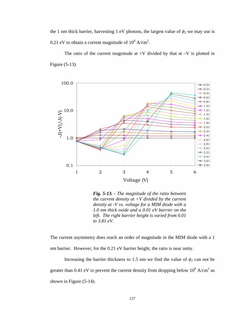
157
the 1 nm thick barrier, harvesting 1 eV photons, the largest value of 2 we may use is
0.21 eV to obtain a current magnitude of 108 A/cm2.
The ratio of the current magnitude at +V divided by that at –V is plotted in
Figure (5-13).
���
���
����
�����
� � � �
� #�$������
�1�����1����
����
����
���
���
�� �
����
����
���
���
�� �
����
����
���
���
�� �
����
����
���
���
�� �
Fig. 5-13. - The magnitude of the ratio betweenthe current density at +V divided by the currentdensity at -V vs. voltage for a MIM diode with a1.0 nm thick oxide and a 0.01 eV barrier on theleft. The right barrier height is varied from 0.01to 3.81 eV.
The current asymmetry does reach an order of magnitude in the MIM diode with a 1
nm barrier. However, for the 0.21 eV barrier height, the ratio is near unity.
Increasing the barrier thickness to 1.5 nm we find the value of 2 can not be
greater than 0.41 eV to prevent the current density from dropping below 108 A/cm2 as
shown in Figure (5-14).

158
������
������
������
������
�����
������
�����
������
�����
�����+
������
� � � �
4� #�$��4������
456������7���-��4�����(���
���
����
����
���
���
�� �
����
����
���
���
�� �
����
����
���
���
�� �
����
����
���
���
�� �
Fig. 5-14. - The current density vs voltage foran MIM diode with a 1.5 nm thick oxide and a0.01 eV barrier on the left. The right barrierheight is varied from 0.01 to 3.81 eV. Thecurrent density needs to be greater than 108
A/cm2 for maximum conversion efficiency. Thecircles are for positive applied bias and the � isfor negative applied bias. For small barrierheights the asymmetry is negligible due to directtunneling and the dash lies below the circle.
Calculating the asymmetry of the MIM diode with a 1.5 nm thick barrier in Figure (5-
15) we find that the asymmetry can reach three orders of magnitude with large 2
values.

159
������
������
������
������
������
������
� � � �
� #�$������
�1�����1����
����
����
���
���
�� �
����
����
���
���
�� �
����
����
���
���
�� �
����
����
���
���
�� �
Fig. 5-15. – The magnitude of the ratio betweenthe current density at +V divided by the currentdensity at -V vs. bias voltage for an MIM diodewith a 1.5 nm thick oxide and a 0.01 eV barrieron the left. The right barrier height is variedfrom 0.01 to 3.81 eV.
The asymmetry for the MIM diode with 2 = 0.41 eV is 2.5 and is nearly constant
across the solar spectrum.
The MIM diode that has a sufficiently high current density with a non-unity
asymmetry has the parameters dox = 1.5 nm, 1 = 0.01 eV, and 2 = 0.41 eV. I
subsequently calculated the J(V) curve in voltage increments of 0.01 V on this
improved MIM diode structure.
I next calculate the conversion efficiency for this improved MIM diode
structure. I assume a diode area of 50 nm x 50 nm with an oxide dielectric constant
of 10. The power out is calculated from JSCQM(V) equation (5.2.25) by locating the

160
maximum of -V�(SCQM(V) within the second quadrant. I then repeat the power
calculation over a range of field strengths.
0 0.5 1 1.5 2� ��
0
0.00005
0.0001
0.00015
0.0002
0.00025
0.0003
rewo
P� W
�
DC Power Out vs. Field Intensity
Fig. 5-16. – The DC power out of the MIMdiode as a function of the photon field strength.The lower blue curve includes the self biasimposed on the MIM diode by the field while theupper red curve neglects this effect.
In Figure (5-16) the red curve neglects the self bias imposed on the MIM diode by the
incident radiation (appropriate for a load in parallel with the MIM diode) while the
blue curve includes this effect (appropriate for a load in series with the MIM diode).
For �>1 multiphoton events become increasingly important. The peak in Figure (5-
16) is due to neglecting these multiphoton events. The self bias is included by

161
iterating between the DC voltage out of the illuminated diode and the applied bias
voltage (set equal to the open circuit voltage) until a self consistent solution is
obtained. For a real load, the self-bias voltage will be less than the open circuit
voltage and the power will lie between the red and blue curve. We find that the
conversion efficiency will be low for low incident field strengths. In an MIM diode
solar cell the field intensities are increased by increasing the photon number (large
area focusing) or increasing the photon confinement (smaller MIM diode).
I next calculate the conversion efficiency of the MIM diode, on a single
photon basis, across the solar spectrum, as shown in Figure (5-17).

162
0.5 1 1.5 2 2.5 3Eph �eV�
0.002
0.005
0.01
0.02
0.05
0.1
noisrevnoC
ycneiciffE
� %�
Conversion Efficiency vs. Eph
Fig. 5-17. – The conversion efficiency for theimproved MIM diode over a range of incidentphoton energies. The self-bias imposed on theMIM diode by the incident photon is included.
The maximum conversion efficiency is around 0.02 % for 1 eV and greater photons.
I then calculate the quantum efficiency, the responsivity times the photon
energy, of the MIM diode at zero bias across the solar spectrum. I did not take
absolute values of the responsivity in the plot resulting in the negative values of
quantum efficiency.

163
0 0.5 1 1.5 2 2.5Ephoton �eV�
�20
�10
0
10
20
30
40
50
EQ
� %�
Fig. 5-18. – The quantum efficiency of the MIMdiode vs photon energy. The negative valuesrepresent rectification reversal.
We find in Figure (5-18) that the quantum efficiency peaks at 50 %, though the
overall conversion efficiency is much less than this value. Consequently, the MIM
diode is only partially limited by the low asymmetry.
The dominant limitation to high conversion efficiency with MIM diodes is the
low field strengths on the MIM diode. We estimate the field strength �)�*ph/Eph as a
function of photon energy across the solar spectrum for our improved MIM diode.

164
������
������
������
������
��� ��� ���� �����
�� � ����������������
α
������
������
������
�����
�SK*�
���*���
$��$�*�������,������
& ,�*�������
/$0�#��������
��
Fig. 5-19. – Estimate of the field strength � vs.photon energy for the improved MIM diode.The plot also includes the conversion betweenphoton energy and wavelength on the right axis.
,�� ��������!-.����������������� ������������+�-��������/��������� ���������� ������
,������������&��0,0�������������������������������$���������� ����������������
square root of dox/(Area �r) where dox is the oxide thickness, Area is that of the MIM
diode and �r is the dielectric constant of the oxide.
To obtain higher efficiencies the photon number must be increased. Since Vph
���� ������������ �� ��������� ����� ���� ������� ����� ��� ���� ������ ��&��� ���������
(5.3.3)), we need to increase the photon number focused upon the MIM diode by
more than three orders of magnitude to increase � to unity.
However, we may have already overestimated Vph by neglecting the MIM
diode resistance and assuming the photon is rectified in a single photon period. A

165
third way to calculate Vph is from the power incident upon the MIM diode by the
solar spectrum over some bandwidth. The current dissipated in a MIM diode at the
oscillation frequency has been calculated by Werthamer (Werthamer, 1966). From
this we may calculate the power absorbed in the MIM diode to be:
+
+
= ∑
∞
−∞=−+ q
nVIqV
JqV
JqV
JVP biasDCn
phn
phn
phnphabs
ωωωω
�
���112
1 (5.5.3)
We then set the power absorbed in the MIM diode equal to the power delivered by the
sun over a 10 nm bandwidth calculated from the 5780 K blackbody approximation to
the solar spectrum Figure (5-1). The photon voltage may then be calculated
numerically from equation (5.5.3), as shown in Figure (5-20). The photon voltage
����������������������������������&���������������quantized the field energy.

166
0.5 1 1.5 2 2.5 3Eph �eV�
1.�10�6
5.�10�60.00001
0.000050.0001
0.0005�
��
Fig. 5-20. – ���� ����� �� � ����� ������divided by the photon energy in eV, as afunction of photon energy for the solarspectrum. It is assumed that 100 % of theincident power is absorbed in the MIM diode. Abandwidth of 10 nm is used.
1��������������&��������������������������$������������������

167
1 1.5 2 2.5 3Eph �eV�
0
5�10�8
1�10�7
1.5�10�7
2�10�7
2.5�10�7
3�10�7
noisrevnoC
ycneiciffE
�%�
Fig. 5-21. – The conversion efficiency as afunction of photon energy across the solarspectrum calculated by setting the powerabsorbed in the MIM diode equal to the incidentsolar power. A bandwidth of 10 nm is assumed.
Figure (5-21) assumes that the solar energy is delivered over a one second
time period. If the photon is harvested in a shorter time the input power and
subsequently Vph increases. The conversion efficiency as a function of alpha is
shown in Figure (5-22), and as predicted, higher efficiencies are possible with higher
$����������

168
0.00001 0.0001 0.001 0.01 0.1 1� ��
1.�10�7
0.00001
0.001
0.1
� %
�
Fig. 5-22. – The conversion efficiency as a������� ��� �� ����� ��������� � �� ��� ��� �
(green) and 3 (blue) eV. The number of photonevents was limited to two for the 1 and 2 eVphotons and to one for the 3 eV photons.
The maximum conversion efficiency possible with this improved MIM diode, as
calculated from the semiclassical quantum analysis, is approximately 1.4 % even for
high intensity illumination and multi-photon events.
Finally, I present the conversion efficiency for an MIM diode with a left
barrier of 0.01 eV. In Figure (5-23) I vary both the oxide thickness and the right
barrier height and calculate the conversion efficiency for 1 eV photons where � is
fixed at one. I have used the WKB approximation to calculate the electron tunneling

169
probability. This is not a realistic situation for solar energy harvesting and neglects
the RC time constant limitations but it will tell us the maximum efficiency that could
be expected for MIM diodes.
���
���
��
��
��
����
����
��� ��� �� �� �� ���
��� ,-&���������
5 �0���- ���88-�-������9�
�����
������
������
�����
�� ���
������
��*��
����*�����
Fig. 5-23. – The conversion efficiency as a functionoxide thickness and barrier height for 1 eV photonswith � equal to 1. Each curve is for a differentbarrier height. The dashed curve is for a 1.5 nmthick oxide with a 0.1 eV left barrier height.
The conversion efficiency is equal to zero when the right and left barrier heights are
equal and the MIM diode is symmetric. As the difference between the right barrier
and left barrier increases so does the conversion efficiency as a result of the increased
asymmetry. The asymmetry and conversion efficiency increase further with thicker
oxides.

170
The efficiency peaks and subsequently decreases for right barriers larger than
0.5 eV. This is a consequence of rectification reversal. As the right barrier height
increases the location of the reversal occurs at larger voltages (approaching the
photon energy in eV). This results in a decrease in the open circuit voltage and
consequently a lower conversion efficiency.
The maximum efficiency we can reach with MIM diodes illuminated with 1
eV photons (�=1) is a function of the antenna impedance. A high impedance antenna
is desirable since it allows matching to a more efficient thicker oxide MIM diode.
We wish to make the left barrier as small as possible. However, we do not want to
choose the right barrier as large as possible due to rectification reversal. An optimal
right barrier is approximately 0.5 eV. An example material system matching this
criterion is Nb and its native oxide with a Cu counter-electrode.
Given the low conversion efficiencies found it is worthwhile to determine
what shape of J(V) curve is able to give us high conversion efficiency. Using the
solar intensities 100 % efficiency can be attained only if the J(V) curve for the MIM
diode has the form of a unit step function with zero current in reverse bias and a
sufficiently high current in forward bias.
For a more realistic situation, consider that the MIM diode has a two-
resistance J(V) form, with a forward bias resistance of RF and a reverse bias
resistance of RR. If we require that
( ) FqVR RJ
Rph
2
1
1
ω�
> (5.5.4)

171
such that the quantum efficiency is equal to 100 % over the voltage range from 0 to
-q·Eph we obtain a maximum conversion efficiency of 25 % with single photon
events. This is true regardless of how small we can make RF (though a large value of
RF will decrease the conversion efficiency).
For this linear diode the efficiency does not increase above 25 % even in the
presence of larger field intensities. Only if the current vs voltage curve of the diode
saturates, exhibiting a resistance higher than RF beyond the saturation voltage, can the
diode exhibit photon stepping and efficiencies greater than 25 % (approaching 100
%).
In addition to the asymmetry requirements needed to obtain a unity quantum
efficiency over a voltage span equal to the photon energy (in eV) the ideal diode must
turn on as close to zero as possible. Additionally, it must saturate as quickly as
possible. If the turn on and saturation occurs in a voltage span small compared to the
photon energy and the incident power is fully absorbed within the MIM diode, high
conversion efficiency may be obtained even with low field intensities. These
requirements are not simultaneously met with MIM diodes.
In conclusion, I have presented the theoretical calculation of semiclassical
rectification and applied it to solar energy conversion with MIM diodes. Broad band
high conversion efficiencies are theoretically possible using a device possessing an
appropriate J(V) curve having high quantum efficiency, large saturating current
magnitudes, a low turn-on voltage, proper impedance matching, and a low
capacitance. Rectification reversal decreases efficiency in the semiclassical case and
further dictates the maximum barrier height that may be used for optimal conversion

172
efficiency. A thick oxide is desirable to increase asymmetry. The maximum oxide
thickness that may be realistically used is dependent upon the antenna resistance. The
conversion efficiencies as a function of field strength for MIM diodes are lower than
that for conventional silicon solar cells even with large field intensities. From
estimates of the expected field strength from the sun it appears that the primary
limitation to solar energy conversion by rectification will be the low field strength.

173
VI. ILLUMINATED MIM DIODE – HOT-ELECTRON THEORY
i. Introduction
In the preceding chapters the incident electromagnetic radiation was coupled
across the oxide of the MIM diode by an antenna. Applying an electric field across
the oxide of an MIM diode is equivalent to applying a bias voltage to the metal
electrodes of the MIM diode. All of the electrons in one electrode are shifted in
energy relative to the opposing electrode. The shift in electron energy occurs for all
electrons within the electrode an equal amount.
A change in the electric field across the oxide results in a change in the slope
of the conduction band edge in the band diagram. The electron tunneling probability
as a function of energy then changes. Consequently, the asymmetry of the MIM
diode I(V) curve when un-illuminated plays a role when the MIM diode is
illuminated.
MIM diodes can exhibit an optical response even when no antenna is used.
The optical response in this case is analogous to the photoelectric effect in metals
(Fowler, 1931). A photon is incident upon the top metal surface of an MIM diode
and couples to a single electron within the metal. The electron is excited up in energy
by an amount equal to the photon energy. At this higher energy the electron
tunneling probability through the barrier increases. The electron tunneling
probability is equal for tunneling in either direction through a barrier so there will be
no asymmetry for tunneling electrons excited in one electrode vs the other.
The excitation of a single electron up in energy does not directly produce an
electric field across the oxide. Therefore, the band and tunneling probability as a

174
function of energy does not change with illumination. Consequently, the illuminated
characteristics produced by hot-electrons will be necessarily different from a MIM
diode coupled to the illumination by an antenna.
ii. Theory
The theory of hot-electron excitation in Al-Al2O3-Au MIM diodes has been
developed by Burshtein and Levinson (Burshtein, 1975). The theory was elaborated
upon and verified experimentally by Marshalek (Marshalek, 1983). Marshalek
included electron scattering within the electrodes that includes the electrons losing
half of their excited energy with every collision.
For a sufficiently thin electrode and narrow bandgap oxide it is possible to
excite carriers within the oxide rather than in the metal. This process has a 10%
quantum efficiency and has a slow response time (Gustafson, 1983). This is because
the excited electrons are subsequently transported in the conduction band of the
oxide, and is a slower process than tunneling.
The electrons in the metal within the energy range between the Fermi level
and a photon energy below the Fermi level are excited in energy (for simplicity I
assume zero degrees Kelvin). The electrons within this energy range are excited with
equal probability (Berglund, 1964). The excitation of electrons in a metal may
subsequently be represented by modifying the Fermi distribution function within the
illuminated metal electrode as shown in Figure (6-1).

175
Fig. 6-1. The modified Fermi distribution functionplotted as a function energy for an illuminatedmetal electrode with hot-electron excitation. The������� �� ��� ��� ���� ����� ��� �� ��� ���� �� ��� �
factor. The temperature is zero degrees Kelvin.
���� ������ �� ��� ���� �� ����� ������� ���� ������ ��� �� ��� ���� �� ��� � ����
representation is applicable when the rate of photon arrival is sufficiently high to
maintain the excited electron distribution depicted in Figure (6-1). Consequently, for
solar intensities this model would only be valid for large area devices.
For solar energy conversion we will want to illuminate the MIM diode on a
single side for maximum photocurrent. Assuming metal 1 is illuminated we may
express the current density vs voltage for the MIM diode as
x
E
xElectronHot dEdEEfVEfETh
mqVJ
x
∫ ∫∞ ∞
−
′−−=0
123)()()(
4)(
π(6.2.1)
f’(E)
E (eV)
Ef
Ef - ��
Ef + ��
���� 1

176
Equation (6.2.1) is the dark current vs voltage expression from Section III with the
modified Fermi distribution function used for metal 1.
This model does not include the multiple photon events that were included in
the quantum rectification models. Furthermore, it does not include the possibility of
exciting electrons which are located more than a photon’s energy below the Fermi
level into the vacated states of previously excited electrons. These stipulations should
be reasonable for low intensity illumination.
The modified Fermi function of the illuminated metal does not conserve the
number of electrons during the excitation process for density of states that varies with
energy. Consequently, the density of electrons excited above the Fermi level due to
incident photons takes the form
)()1)(()()()( ωθω �� −−−+= EfEgEfEgEn (6.2.2)
in the energy range of the Fermi level to a single photon energy above the Fermi
������������������������������ ������������������������������������ �����
energy in the range of the Fermi level to a single photon energy above the Fermi
level.
)(
)()(
Eg
EgE
ωθθ �−=′ (6.2.3)
Equation (6.2.3) is valid for an arbitrary density of states g(E).

177
The distribution of electrons as a function of energy is nearly equivalent for
excitation by hot-electrons and the absorption spectrum in the semiclassical quantum
model. The expression for the tunneling probability as a function of energy for the
two models is inequivalent due to the shift in the band diagram that occurs with an
antenna coupled MIM diode that does not occur for hot-electron excitations in the
electrode of an MIM diode. Consequently, the illuminated current density vs voltage
curves are not equivalent. This is not surprising since the semiclassical quantum
model neglects interactions within the electrodes.
iii. Hot-Electron Solar Cells
For a solar cell operating by hot-electron excitations there will be an
equivalent of a bandgap. Only electrons excited above or near the barrier height of
the MIM diode are likely to tunnel across. Thus photons with an energy lower than
the larger of the two barriers in the MIM diode are not collected efficiently.
Since all electrons within a photon energy below the Fermi level are excited
with equal probability only a fraction will have sufficient energy to tunnel through the
barrier. For low energy photons almost all of the excited electrons will be unable
tunnel through the barrier. Even if an electron is excited there is a chance it relaxes
and re-emits the incident photon, or that the energy is lost to heat. Furthermore, the
tunneling probability decreases substantially below unity if the electron momentum is
not perpendicular to the barrier.
The energy of the photon will not be harvested with 100 % efficiency if the
electron thermalizes after tunneling through the oxide. Thermalization of the

178
tunneling electron is likely given that the hot electron distance is approximately 10
nm (Eckertova, 1976). Therefore, electrons excited far above the conduction band of
the insulator may have a large probability of tunneling across, but will subsequently
thermalize within the second metal before reaching the load and energy will be lost.
In order to use the photon energy fully, for the fraction of electrons which are
excited and tunnel through the barrier, we must make the MIM diode small enough
that a single tunneling electron is sufficient to change the Fermi level within the
receiving electrode. Equating the energy stored in the MIM diode treated as a
capacitor to the incident photon energy we have:
2
2
1MIMMIM VC=ω� (6.2.4)
The tunneling of n electrons across a barrier produces a voltage of
MIMMIM C
qnV
⋅= (6.2.5)
Consequently, by solving for the capacitance CMIM in equation (6.2.5) and
substituting into equation (6.2.4) we find that the voltage produced by the MIM diode
must be equal to
q
EV ph
ph
2= (6.2.6)

179
This may be accomplished for photons of a single energy by making the capacitance
of the MIM diode equal to
phMIM E
qnC
⋅⋅=
2(6.2.7)
Let’s assume we have a MIM diode with a 10 nm thick oxide, a dielectric
constant of 10, and can harvest 1 eV photons with approximately 100 % quantum
efficiency. If we assume that a single photon is incident upon the device and we want
this photon to result in the tunneling of an electron which produces a voltage change
equal to the photon energy we require that CMIM = 8 � 10-20 F. To obtain this
capacitance we must make the diode area 3 nm � 3 nm.
Once we have made the MIM diode this small two additional features play a
role. First, we may be limited to the tunneling of a single electron by the coulomb
blockade (Koch, 1992). Coulomb blockade is when the tunneling of a single electron
produces a potential sufficiently high to prevent the tunneling of further electrons.
Given the photon arrival rate from the sun this should not pose a significant problem.
Second, the potential produced by this electron will be lost if the MIM diode
does not prevent the electron from tunneling back to the emitting electrode. We must
illuminate the MIM diode on the side that minimizes the bounce-back of the
tunneling electrode. This depends on the size of the voltage produced and the
location of the rectification reversal point. For low voltages we will illuminate on the
low-barrier side of the MIM diode, for high voltages we want to illuminate on the
high-barrier side of the MIM diode. Since we initially assumed that the photon

180
energy is larger than both of the barriers (or nearly as large), the generated voltage
will be nearly as large as the two barriers. A thick barrier will not substantially
reduce the tunneling probability of highly excited electrons but will substantially
reduce the probability the electron returns to the emitting electrode. Consequently,
the photon energy can be dissipated within the load.
We can deduce that a hot-electron MIM solar cell will be less efficient than
conventional semiconductor based solar cells. The quantum efficiency for
semiconductor solar cells is near unity, which will not be the case in the hot-electron
solar cell.
Consider a MIM diode with a 10 nm thick oxide, and a symmetric barrier 0.6
eV in height illuminated by 1 eV photons. The top metal is sufficiently thin such that
photoexcited electrons arrive at the metal-oxide interface without suffering a
collision. For a 1 eV photon impinging a 0.6 eV barrier the probability of tunneling
across is near 100 %. If we assume that the area of the device is approximately 3 nm
� 3 nm the voltage generated due to the tunneling electron will be equal to two times
the photon energy. The probability the electron tunnels back to the emitting electrode
can be calculated to be negligible. Consequently, the energy collection efficiency can
be approximately 100 %.
The 100 % efficiency assumes that all incident photons excite a carrier from
the Fermi level and the excited carrier moves perpendicular towards the barrier (and
does not reflect the incident photon or thermalize prior to tunneling). The tunneling
probability decreases for carriers that are not incident perpendicular to the barrier.
For a typical situation, we find that the tunneling probability decreases by an order of

181
magnitude for carriers that are approximately 18� off of normal incidence of a 1 nm
thick barrier (Waters, 1999). This implies that only 2 % of the carriers will be within
the acceptance angle. Consequently, the efficiency drops to less than 2 %.
We must further consider that excitation of carriers deep below the Fermi
level occurs with equal probability as exciting carriers near the Fermi level.
Assuming only carriers that are within 0.4 eV of the Fermi level are excited with
sufficient energy to traverse the barrier then only 40 % of the incident 1 eV photons
produce a carrier, further reducing the efficiency to less than 0.8 %. The 40 % may
be remedied by employing a quantum well in the emitting electrode to ensure all
carriers are excited between a specific set of energy levels.
This efficiency is for a single photon energy. Photon energies much lower
than the barrier height will not be collected and those greater than 1 eV will not have
the photon energy fully collected. Even for the optimal photon energy we predict less
than 0.8 % efficiencies. Although, under certain situations, this hot-electron solar cell
may be more efficient than a solar cell comprised of an antenna coupled MIM diode
(e.g., when the rectifying MIM diode is not sufficiently nonlinear for the incident
photon), the efficiency is substantially lower than conventional silicon solar cells.

182
VII – RESONANT TUNNELING MIIM DIODES
i. Motivation
MIM diodes show less asymmetry and nonlinearity than desired. The low
asymmetry and nonlinearity are partially responsible for the low solar energy
conversion efficiency. We would like a diode with increased asymmetry for linear
rectification and increased nonlinearity for square-law rectification. Furthermore, to
obtain high conversion efficiency we require sufficiently high current magnitudes and
low turn-on voltages.
One approach to improve the MIM diode asymmetry is by using two different
electrodes, each with a different density of states. By making one of the electrodes a
standard metal and the second electrode of a semiconductor, semi-metal,
superconductor, superlattice or a quantum well, we can introduce additional
asymmetry into the system. The disadvantage of this approach is the lower
conductivity of other electrodes. It is preferable to use metals as the electrode
material to maintain high conductivity.
An alternative approach to achieve asymmetry is to change the conduction
mechanism in forward vs reverse bias. However, we want tunneling to provide the
conduction mechanism in-order to maintain fast response times. In addition to the
standard Fowler-Nordheim and direct tunneling observed in MIM diodes, a third
possibility is resonant tunneling. Increased asymmetry may be achieved by making
the electrons traverse the oxide by resonant tunneling under one polarity of bias and
standard tunneling under the other polarity. This situation can be realized by using a
multilayer structure between the electrodes instead of the single oxide layer. The

183
multilayer structure may be composed of various combinations of insulators, metals,
semiconductors, semimetals, superconductors, quantum wells, or superlattices.
Resonant tunneling is not a new phenomenon. Esaki tunnel diodes use
resonant tunneling and the negative differential resistance associated with
semiconductors (Mizuta, 1995). More recently Yukio has fabricated a triple barrier
resonant tunneling diode using the GaInAlAs system and observed the gradual
change from classical rectification to photon assisted tunneling (Oguma, 1999).
Nobuo, using the same triple barrier structure as Oguma, with an improved antenna,
observed the multi-photon process involved with photon assisted tunneling at 3.1 THz
(96.8 ���� �Sashinaka, 2000). Di Ventra proposed a theoretical diode out of the
InGaAs system that uses two adjacent oxides as opposed to the quantum wells formed
with alternating metals and oxides (Di Ventra, 1996). To my knowledge the device
proposed by Di Ventra was never realized in practice. A similar InGaAs structure
that used a symmetric barrier was later proposed by Korotkov for use in non-volatile
memory (Korotkov, 1999).
Resonant tunneling devices fabricated entirely out of metals and insulators are
scarce. Watanabe has made double and triple barrier resonant tunneling devices with
epitaxially grown single crystalline metals and insulators (Suemasu, 1994). The
material system was CoSi2 (metal) and CaF2 (insulator). The choice of metals and
insulators is restricted to those that lattice-match the substrate. With the advent of
atomic layer deposition, it is possible to form multilayer structures composed of
metals and insulators. We are no longer limited to the native oxides of the base
metals but can instead deposit a variety of different oxides by using ALD. Depositing

184
metals with ALD makes it possible to form amorphous equivalents of Suemasu’s
multibarrier structures, in addition to superlattices. Furthermore, it becomes feasible
to put multiple insulators adjacent to one another.
The device I proposed uses two adjacent oxides in place of the single oxide
layer found in MIM diodes. Using atomic layer deposition, a second oxide may be
deposited onto the native oxide of the base metal. This device may be easily
fabricated using a wider range of materials than possible with epitaxial techniques
previously used to fabricate resonant tunneling devices. The remainder of this section
presents the metal-insulator-insulator-metal (MIIM) diode.
ii. MIIM Diode Theory
The MIIM diode utilizes two adjacent insulators, sandwiched between the
metal electrodes, instead of one. These two insulators have different electron
affinities and consequently result in a discontinuity at their interface. The equilibrium
band diagram for one such MIIM structure is shown in Figure (7-1).

185
9
9.5
10
10.5
11
11.5
12
12.5
13
-6 -3 0 3 6 9Distance ( nm )
Ene
rgy
( eV
)
Metal 1 Metal 2Insulator Insulator
�����
�����
�����
Fig. 7-2. Energy band diagram for aCr/Cr2O3/Al2O3/Cr MIIM diode in equilibrium.
The barrier heights are determined by the workfunctions �1 and �2 of the two metal
electrodes and electron affinities �1 and �2 of the two adjacent insulators.
The energy band diagram under an applied bias is shown in Figure (7-2).
With a negative bias voltage applied to metal 2 we encounter a combination of
Fowler-Nordheim and direct tunneling. When a positive voltage is applied to metal 2
a quantum well forms at the interface of the two oxides.

186
8
9
10
11
12
13
14
-6 -3 0 3 6 9Distance ( nm )
Ene
rgy
( eV
)
Bias Voltage = 1.95 V
No Bias Voltage
Bias Voltage = -1.2 V
Resonant Energy Level
Quantum Well
Fig. 7-2. Energy band diagram for aCr/Cr2O3/Al2O3/Cr MIIM diode shown inequilibrium and with both polarities of applied bias.Positive applied biases create a quantum well in thefirst oxide adjacent to the dual oxide interface.
Within the quantum well the allowed energy levels are quantized (the lowest
quantized energy level within the well is shown with the dashed line). As shown in
Figure (7-3), the tunneling probability through these quantized energy levels is higher
than the tunneling probability for adjacent energy levels.

187
������
������
�����
�����
������
������
������
�����
�����
������
������
������
�����
�����
������
������
� �� �� �� �� � �
��������������
�����
���
���
���
��
��
��
��
�
�
�
�� ������
���
Fig. 7-3. Electron tunneling probability as afunction of energy superimposed upon the banddiagram of the MIIM diode. The resonant energylevels formed within the quantum well (shown onthe band diagram) produce an increased tunnelingprobability through the structure.
As shown in Figure (7-4), the resonant tunneling energy levels introduce a
substantial asymmetry into the current vs voltage curve for positive applied voltages
compared to negative applied voltages.

188
������
������
�����
������
�����
�� �� �� � � � �
����������������
����
�����
!"������#��$%�� ����&'(�����
Fig. 7-4. The calculated current density vs voltagecurve for the MIIM diode shown in Figure (7-2).Calculations made at 300 K (green) and 77 K(blue).
This asymmetry is made vividly clear on a linear current density scale as
shown in Figure (7-5).

189
�����
����
����
����
����
�� �� �� � � � �
����������������
!"�������#��$%������&'(�����
Fig. 7-5. The calculated current density vs voltagecurve for the MIIM diode shown in Figure (7-2)plotted on a linear current density scale.
For electrodes with a band gap, or variable density of states, resonant
tunneling in this dual insulator structure results in a region of substantial negative
differential resistance. In the MIIM diode we do not see a negative differential
resistance.
iii. Experimental MIIM Diode
I have fabricated several MIIM diodes using atomic layer deposition to form
the second insulator. The devices were fabricated using the lithographic MIIM mask
presented in Section II. The MIIM diode was fabricated on a silicon substrate with a
thermally grown oxide layer. Contact pads were made using 100 nm of Cr covered

190
by 100 nm of Au. The Au metal prevented complete Al2O3 coverage and allowed
contact to be made to the device after the ALD deposition. The base metal was
formed of Cr and allowed to oxidize to form Cr2O3. Subsequently 3 nm of Al2O3 was
deposited by atomic layer deposition. Top contacts were formed of Ag.
The experimental current vs voltage curve for the MIIM diode is shown in
Figure (7-6).
�
�
�
�
�
���� ��� ��� �� ���
���������������
)%�����*�%+��,-,
#"���*�%+��,--,
��
��
�
��
!"������#��$%�� ������
&'(�
���
��
Fig. 7-6. Experimental data for an MIIM diode anda typical MIM diode. The MIM curve has beenmultiplied by 10-6 to allow the two devices to beplotted on the same linear scale. This comparisonis valid for thick oxide layers.
The current vs voltage curve was stable under reverse bias and repeated itself. The
forward bias portion of the curve showed drastic nonlinearity as expected. The
forward bias portion of the curve did not repeat itself and the current magnitude

191
fluctuated from one measurement to the next. However, the dramatic nonlinearity
was present for each voltage sweep regardless of voltage sweep direction.
The experimental current vs voltage curve agrees with theory only
qualitatively. The current magnitudes do not. I suspect the disagreement is due in
part to surface states at the interface between the Cr2O3/Al2O3. The yield on these
devices was very low (1/500). The low yield I suspect was due to the poor nucleation
of the ALD layer to the native chromium oxide as most devices measured did not
have low current magnitudes or a decreased capacitance as would be expected if the
ALD layer was present. Recent experiments indicate that the nucleation may be
improved by increasing the precursor concentrations.
iv. Solar Energy Conversion Efficiency
The current vs voltage curve in Figure (7-6) shows some of the characteristics
required for high conversion efficiency. The asymmetry is larger than the MIM diode
in forward vs reverse bias directions and the knee of the curve is located at lower
voltages than the MIM diode. However, the solar energy conversion efficiency of the
experimental MIIM diode would be uselessly low due to the low current densities.
I use an MIIM diode based upon the improved MIM diode from Section V to
estimate the solar energy conversion efficiency of an MIIM diode. For the MIIM
diode the left barrier is chosen as 0.01 eV, the right barrier is 0.41 eV, and the oxide
interface barrier is 0.4 eV. These values are chosen directly from the improved MIM
diode from Section V. The left oxide is 1 nm thick and the second oxide is set to 0.5
nm thick. The J(V) curve for both the improved MIM diode and the MIIM diode are

192
shown in Figure (7-7). The thinner oxide layers and smaller barriers in this
theoretical MIIM diode result in higher current magnitudes than the experimental
MIIM diode. The MIIM diode shows a slightly larger current magnitude and
asymmetry over the MIM diode.
.���
�����
�����
������
������
������
������
� � � �
�����������
!"������#��$%�������&'(�
��� ��
,--,
,-,
Fig. 7-7. The current density vs voltage curve for theoptimized MIM diode from Section V and an MIIMdiode based upon the improved MIM diode.
I calculated the solar energy conversion efficiency assuming the diode area is
50 nm x 50 nm. The semiclassical quantum mechanical J(V) theory is used to
calculate the power out of the MIIM diode. I assumed that the antenna is 100 %
efficient at transferring the incident photons electric field across the oxide of the
diode and that the diode fully absorbs the incident power.

193
The photon voltage across the MIIM diode is calculated from the solar
spectrum which is approximated by a 5780 K blackbody. The �, the photon voltage
divided by the photon energy, is plotted in Figure (7-8).
1 1.5 2 2.5 3Eph �eV�
0
5�10�6
0.00001
0.000015
0.00002
0.000025
0.00003
���
Fig. 7-8. The � (the photon voltage times the photonenergy) as a function of the photon energy on the MIIMstructure across the solar spectrum.
The values of � are approximately an order of magnitude lower than those obtained
with the MIM diode due to the lower resistance of the MIIM diode.
The solar energy conversion efficiency vs photon energy across the solar
spectrum is shown in Figure (7-9).

194
1 1.5 2 2.5 3Eph �eV�
0
2.5�10�8
5�10�8
7.5�10�8
1�10�7
1.25�10�7
1.5�10�7
noisrevnoC
ycneiciffE
� %�
Fig. 7-9. The conversion efficiency for the MIIM diodeover a range of incident photon energies.
The MIIM diode has a maximum conversion efficiency of approximately 1.6 � 10-7
%. The optimized MIM diode obtained an efficiency of 3.2 � 10-7 %. The decrease
in efficiency is due to the lower photon voltage produced across the MIIM diode as
opposed to the MIM diode.
A higher power incident on the MIM diode will result in an increase in �.
�������� ������������� �������������� � �������������������

195
0.0001 0.001 0.01 0.1 1� ��
0.00001
0.001
0.1
10
�� %
�
Fig. 7-10. The conversion efficiency as a functionof � for photon energies of 1 eV (red points), 2 eV(green points) and 3 eV (blue points). The numberof photon events was limited to two for the 1 eVphotons and one for the 2 and 3 eV photons.
For high field intensities, the MIIM diode produces higher conversion
efficiencies than the improved MIM diode from Section V due to the larger current
density and greater asymmetry in the MIIM diode current vs voltage curve. The
maximum conversion efficiency of this MIIM diode, calculated using the
semiclassical quantum approach, is approximately 4 %. The roll-off and maximum
efficiency limit is due to the MIIM diode.
Finally, I calculate the quantum efficiency of the MIIM diode at zero bias as a
function of photon energy, shown in Figure (7-11).

196
0 0.5 1 1.5 2 2.5Ephoton �eV�
0
20
40
60
EQ
� %�
Fig. 7-11. The quantum efficiency of the MIIM diode.
The quantum efficiency of the MIIM diode reaches approximately 60 % for 1.2 eV
photons. The improved MIM diode produced a maximum quantum efficiency just
under 50 %. This improvement can be attributed to the greater asymmetry in the J(V)
curve.
In conclusion, although the particular MIIM diode structure presented is an
improvement over the single layer MIM diode structure, low efficiencies are still
obtained due to the low field intensity.

197
VIII – CONCLUSIONS AND RAMIFICATIONS
I have explored the possibilities of using MIM diodes for solar energy
harvesting assuming an ideal antenna. Actual efficiencies obtained will likely be
lower than what I have predicted once a realistic antenna is incorporated.
I have fabricated MIM diodes from Ti, Ni, Cr, Al, and Nb base metals using
several different fabrication techniques. The current vs voltage curves of the MIM
diodes were measured and calculated from theory. The forward vs reverse bias
asymmetry, area scaling, and relative current magnitude shifts could be predicted.
The current magnitude and curvature did not match the experimental data when
literature values for material parameters were used. To obtain a better fit with theory,
without arbitrarily adjusting material parameters, multiple experiments would be
necessary to isolate barrier heights and oxide thicknesses (thermal, optical, and
destructive).
The processing of the oxide layer played a critical role in MIM diode
performance. The oxidation method, conditions, substrate, cleanliness, oxidation
time, temperature, ion incorporation, plasma processing, measurement techniques,
and metals all affect the MIM diode performance. The processing steps required to
fabricate a functional MIM diode are very unforgiving.
The various models applicable to illuminated MIM diodes have been explored
for solar energy conversion. Due to the broad frequency range that the MIM diode is
subjected to by the sun both classical and quantum models are explored. In the
classical regime the current models are limited by the approximations used.

198
Consequently, I developed a PSpice model applicable to MIM diodes. The PSpice
model has the unique ability to incorporate the rectification reversal effect found to
occur in MIM diodes. Furthermore, the PSpice model is not limited to MIM diodes
but is equally applicable to many other electron devices.
As the frequency increases the size of the incident electromagnetic quanta
becomes large on a voltage scale equal to the photon energy (divided by q) these
classical models are no longer valid. The quantitative frequency ranges for the
various illuminated models presented in Figure (1-3) depend upon the explicit shape
of the diodes J(V) curve. For most MIM diodes the nonlinearity over a voltage span
equal to the photon energy (times q) of visible light warrant use of the semiclassical
models. For example, in Figure (8-1) I plot the responsivity at zero volts for the
improved MIM diode as a function of photon energy.

199
0 0.5 1 1.5 2 2.5 3Ephoton �eV�
�0.4
�0.2
0
0.2
0.4ytivisnopse
R� 0�
� A� W
�
Fig. 8-1. The responsivity (without taking theabsolute value) as a function of photon energy. Forthe improved MIM diode the classical result is incorrect within 10 % for energies less than 0.14 eV(corresponding to a 8.86 �m wavelength). Forshorter wavelengths the semiclassical theory mustbe used.
The classical theory is correct within 10 % for incident wavelengths longer than 8.86
�m).
Efficiencies greater than 25 % become possible with these quantum models
with the aid of photon stepping. I have shown that with a perfect photon step 100 %
conversion efficiencies can be obtained. However, the intensity of the solar spectrum

200
and nonlinearity attainable with MIM diodes limit the efficiencies to much lower
values.
I calculated the conversion efficiencies as a function of photon energy, field
intensity, and the diode structure. Estimates of the field intensity coupled to the
insulator of the MIM diode by the sun were made. The limitations of the
semiclassical model became evident due to the low photon numbers involved.
Despite these limitations, I was able to use the semiclassical theory to predict what is
needed in an MIM diode structure to obtain high efficiencies: small capacitance, high
current magnitudes, large asymmetries (responsivity) and low turn on voltages.
Conversion efficiencies less then 1 % were calculated.
I considered making a hot-electron solar cell where no electric field is
imposed across the oxide due to the incident photon. This situation occurs when an
antenna is not used. In the semiclassical theories, there is a link between the energy
of the incident photon and the voltage induced across the structure and as a result
efficient conversion over a range of photon energies is possible. To make an efficient
hot-electron solar cell this link must be built into the device. I have shown that for a
hot-electron solar cell to be efficient, for a single photon energy, the diode must be
made sufficiently small such that the tunneling of a single electron can substantially
alter the voltage across the oxide. The voltage change due to the tunneling of a single
electron is an effect that should be included in future work on the semiclassical
theories as well. The final efficiency is estimated to be less than 1 % for the hot-
electron solar cell for a single energy. Although this efficiency may be higher than
the MIM diode functioning as a rectifier in conjunction with an antenna, the hot-
201
electron solar cell will be less efficient then conventional semiconductor solar cells.
Furthermore, unlike the rectifying MIM diode using photon stepping, the hot-electron
solar cell will only collect photons of a single energy efficiently.
Finally, I developed an improved metal-insulator based device based upon an
extension of the MIM diode. The MIIM diode produces an enhanced nonlinearity by
incorporating two adjacent oxides instead of the single oxide layer of the MIM diode.
In the MIIM diode the mode of tunneling under positive applied biases can be made
different from that under negative applied biases resulting in improved asymmetry.
The improved asymmetry was predicted by an extension of the MIM diode
calculations. MIIM diodes were fabricated using atomic layer deposition to deposit
the second oxide layer and produced a substantial increase in nonlinearity over the
single layer MIM diodes. The MIIM diode incorporates some of the improvements
required for efficient energy harvesting.
In closing, obtaining high efficiency over a wide range of photon energies
may be accomplished by rectification and the resulting photon steps. The solar
energy conversion efficiencies are substantially lower than conventional
semiconductor based solar cells. The primary limitation is due to the low field
strengths imposed across the MIM diode by the solar intensity. Even if the field
intensities are substantially increased, the conversion efficiencies for MIM diodes
with acceptable impedances are less than conventional semiconductor solar cells.
This is because of rectification reversal and because the MIM diode does not
simultaneously attain high quantum efficiencies, low turn-on voltages, high current
magnitudes and small capacitance.

202
BIBLIOGRAPHY
Agilent Technologies, 395 Page Mill Road, P.O. Box 10395, Palo Alto, CA 94306,(650) 752-5000, (2001).
Alessandrini, E.I., Brusic, V., “Effect of Varying Oxidizing and Nitriding Parameterson the Surface of Cr Thin Films”, Journal of Vacuum Science and Technology, 9, 83,(1972).
Anderson, L.M., “Harnessing Surface Plasmons for Solar Energy Conversion”, SPIE– Integrated Optics III, 408, 172, (1983).
Ashcroft, N.W., Mermin, N., Solid State Physics, Saunders College, Philadelphia,(1976).
AutoDesk Incorporated, 111 McInnis Parkway, San Rafael, CA 94903, (415) 507-5000, (2001).
Aversa, C., Keay, B.J., “Virtual States and Photon-Assisted Tunneling”, PhysicalReview B, 54, R2284, (1996).
Baird, K.M., “Frequency Measurement of Optical Radiation”, Physics Today,January, 51, (1983).
Bardeen, J., “Surface States and Rectification at a Metal Semi-Conductor Contact”,Physical Review, 71, 717, (1947).
Berglund, C.N., Spicer, W.E., “Photoemission Studies of Copper and Silver :Experiment”, Physical Review, 136, A 1044, (1964)
Borland Software, Inc., 100 Enterprise Way, Scotts Valley, CA 95066-3249, (831)431-1000, (2001).
Bube, R.H., Fundamentals of Solar Cells, Academic Press, New York, (1983).
Burshtein, Z., Levinson, J., “Photo-Induced Tunnel Currents in Al-Al2O3-AuStructures”, Physical Review B, 12, 3453, (1975).
Burstein, C., Lundqvist, S., Tunneling Phenomena in Solids, Plenum Press, NewYork, (1969).
Cahalan, R.F., http://climate.gsfc.nasa.gov/~cahalan/Radiation/, NASA-Goddard, 913Greenbelt, MD 20771 (1999).

203
Campbell, S.A., The Science and Engineering of Microelectronic Fabrication,Oxford University Press, New York, (1996).
Cerac, Inc., 407 N. 13th Street, Milwaukee, WI 53233-2201, (414) 289-9800 (2001).Climent, F., Capellades, R., “Anodic Oxidation of Titanium at Low Voltages”,Materials Letters, 18, 263, (1993).
Champlin, K.S., Eisenstein, G., “Cutoff Frequency of Submillimater Schottky-BarrierDiodes”, IEEE Transactions on Microwave Theory and Techniques, MTT-26, 31,(1978).
Cohen, E.R., Taylor, B.N., “The Fundamental Physical Constants”, Physics Today,August, BG7, (1997).
Dayem, A.H., Martin, R.J., Physical Review Letters, 8, 246, (1962).
Deeley, P.M., Electrolytic Capacitors; The Theory, Construction, Characteristics,and Application of All Types, The Cornell-Dubilier Electric Corporation, New Jersey,(1938).
Diesing, D., Hassel, A.W., Lohrengel, M.M., “Aluminum Oxide Tunnel Junctions:Influence of Preparation Technique, Sample Geometry and Oxide Thickness”, ThinSolid Films, 342, 282, (1999).
Di Ventra, M., Papp, G., Coluzza, C., Baldereschi, A., Shulz, P.A., “Indented BarrierResonant Tunneling Rectifiers”, Journal of Applied Physics, 80, 4174, (1996).
Duke, C.B., Tunneling in Solids, Academic Press, New York, (1969).
Dunne, P.J., Collins, R.A., “Measurement Techniques in MIM DeviceCharacterization”, International Journal of Electronics, 68, 373, (1990).
Eckertova, L., Dvorak, J., Bocek, J., “The Range of Hot Electrons in Thin MetalFilms Determined by the Electron Emission from MIM Structures”, Thin Solid Films,36, 171, (1976).
Elchinger, G.M., Sanchez, A., Davis, C.F., Javan, A., “Mechanism of Detection ofRadiation in a High-Speed Metal-Metal Oxide-Metal Junction in the Visible Regionand at Longer Wavelengths”, Journal of Applied Physics, 47, 591, (1976).
Eliasson, B., Moddel, G., “Optically Addressed SLM Incorporating a CuInGaSe2/a-Si:H Heterojunction, Spatial Light Modulators”, Technical Digest1999, OSATechnical Digest Snowmass, 97, (1999).
Emery, K., “The Rating of Photovoltaic Performance”, IEEE Transactions onElectron Devices, 46, 1928, (1999).

204
Entegris, Inc., 3500 Lyman Boulevard, Chaska, MN 55318 1-800-394-4083 (2001).
Jennings, D.A., Evenson, K.M., Knight, D.J.E., “Optical Frequency Measurements”,Proceedings of the IEEE, 74, 168, (1986).
Fan, J., Sugioka, K., Toyoda, K., “Low-Temperature Growth of Thin Films of Al2O3
by Sequential Surface Chemical Reaction of Trimethylaluminum and H2O2”,Japanese Journal of Applied Physics, 30, L1139, (1991).
Faris, S.M., Gustafson, T.K., Wiesner, J.C., “Detection of Optical and InfraredRadiation with DC-Biased Electron-Tunneling Metal-Barrier-Metal Diodes”, IEEEJournal of Quantum Electronics, QE-9, 737, (1973)
Foden, C.L., Whittaker, D.M., “Quantum Electrodynamic Treatment of Photon-Assisted Tunneling”, Physical Review B, 15, 12617, (1998).
Fonash, S.J., Solar Cell Device Physics, Academic Press, New York, (1981).
Fowler, R.H., “The Analysis of Photoelectric Sensitivity Curves For Clean Metals atVarious Temperatures”, 33, (1931).
Fowler, R.H. , Nordheim, L., “Electron Emission in Intense Electric Fields”,Proceedings of the Royal society of London A., 173, (1928).
Fu, C.Y., Van Duzer, T., “A New Lead Alloy For Josephson Junctions”, IEEETransactions on Magnetics, MAG-17, 290, (1981).
Fumeaux, Herrman, “Nanometer Thin Film Ni-NiO-Ni Diodes for Detection andMixing of 30 THz Radiation”, Infrared Physics and Technology, 39, (1998)
George, S.M., Dillon, A.C., Ott, A.W., Way, J.D., “Surface Chemistry of Al2O3
Deposition Using Al(CH3)3 and H2O in a Binary Reaction Sequence”, SurfaceScience, 322, 230, (1995).
Geppert, D.V., “Space-Charge-Limited Tunnel Emission into an Insulating Film”,Journal of Applied Physics, 33, 2993, (1962).
Gewinner, G., Peruchetti, J.C., Jaegle, A., Kalt, A., “Photoemission Study of theChromium (111) Surface Interacting with Oxygen”, Surface Science, 78, 439, (1978).
Griffiths, D.J., Introduction to Quantum Mechanics, Prentice-Hall, New Jersey,(1995).
Grober, R.D., Schoelkopf, R.J., Prober, D.E., “Optical Antenna: Towards a UnityEfficiency Near-Field Optical Probe”, Applied Physics Letters, 70, 1354, (1997).

205
Gundlach, K.H., “Theory of Metal-Insulator-Metal Tunneling for a Simple Two-BandModel”, Journal of Applied Physics, 44, 5005, (1973).Gustafson, T.K., “Coherent Conversion of the Sunlight Spectrum Final Report”,NASA Grant NAG 3-88, University of California, Berkeley, (1982).
Hocker, L.O., Sokoloff, D.R., Daneu, V., Szoke, A., Javan, A., “Frequency Mixing inthe Infrared and Far-Infrared Using a Metal-To-Metal Point Contact Diode”, AppliedPhysics Letters, 12, 401, (1968).
Hübers, H.W., Schwaab, G.W., Röser, H.P., “Video Detection and MixingPerformance of GaAs Schottky-Barrier Diodes at 30 THz and Comparison withMetal-Insulator-Metal Diodes”, Journal of Applied Physics, 75, 4243, (1994).
International Products Corporation, P.O. Box 70, Burlington, NJ 08016, (609) 386-8770, (2001).
Iscoff, R., “Wafer Cleaning: Wet Methods Still Lead the Pack”, SemiconductorInternational, 16, 58, (1993).
Johnson, R.C., Antenna Engineering Handbook, 3rd edition, McGraw-Hill, NewYork, (1993).
J.T. Baker, 222 Red School Lane, Phillipsburg, NJ 08865, 1-800-JTBAKER, (2001).
Kale, M.B., “Electron Tunneling Devices in Optics”, Optical Engineering, 24, 267,(1985).
Kalra, K.C., Singh, K.C., Singh, M., “Formation of Anodic Oxide Films on Titaniumin the Presence of Ultraviolet Radiation”, Indian Journal of Chemistry, 33A, 732,(1994).
Kittel, C., Introduction to Solid State Physics, 6th edition, John Wiley and Sons, NewYork, (1986).
Koch, H., Lübbig, H., Single-electron Tunneling and Mesoscopic Devices, Springer-Verlog, New York, (1992).
Korotkov, A., Likharev, K., “Resonant Fowler-Nordheim Tunneling ThroughLayered Tunnel Barriers and its Possible Applications”, International Electron DeviceMeeting, Technical Digest, Washington DC, (1999).
Kroemer, H., Quantum Mechanics For Engineering, Materials Science, and AppliedPhysics, Prentice Hall, New Jersey, (1994).
Landauer, R., Martin, Th., “Barrier Interaction Time in Tunneling”, Reviews ofModern Physics, 66, 217, (1994).

206
Levy, “Very Small Tunnel Junctions Sense the Effect of Single Electrons”, PhysicsToday, 41, 19, (1988).
Lichtenberger, A.W., Lea, D.M., Lloyd, F.L., “Investigation of Etching Techniquesfor Superconductive Nb/Al-Al2O3/Nb Fabrication Processes”, IEEE Transactions onApplied Superconductivity, 3, 2191, (1993).
Loudon, R., The Quantum Theory of Light, 3rd edition, Oxford University Press,Oxford, (2000).
Maissel, L.I., Glang, R., Handbook of Thin Film Technology, McGraw-Hill, NewYork, (1970).
Mathworks, Inc., 3 Apple Hill Drive, Natick, MA 01760-2098, (508) 647-7000,(2001).
Marshalek, R.G., Davidson, F.M., “Photoresponse Characteristics of Thin-FilmNickel-Nickel Oxide-Nickel Tunneling Junctions”, IEEE Journal of QuantumElectronics, QE-19, 743, (1983).
Martin, S. et al, “Fabrication of 200 to 2700 GHz Multiplier Devices Using GaAs andMetal Membranes”, IEEE MTT-S Digest, Phoenix, AZ, (2001).
Microsoft, One Microsoft Way, Redmond, WA 98052-6399, (425) 882-8080, (2001).
Mizuta, H., Tomonori, T., The Physics and Applications of Resonant TunnellingDiodes, Cambridge University Press, New York, (1995).
Neamen, D.A., Semiconductor Physics and Devices : Basic Principles, Irwin,Homewood, IL, (1992).
Oguma, Y., Sashinaka, N., Asada, M., “Terahertz Response with Gradual Changefrom Square-Law Detection to Photon-Assisted Tunneling in Triple-Barrier ResonantTunneling Diodes”, Japanese Journal of Applied Physics, 38, L717-L719, (1999).
Papp, G., Di Ventra, M., Coluzza, C., Balderschi, Al, Margaritondo, G., CurrentRectification Through a Single-Barrier Resonant Tunneling Quantum Structure,”Superlattices and Microstructures, 17, 273, (1995).
Penley, J.C., “Tunneling Through Thin Films with Traps”, Physical Review, 128,596, (1962).
Pierret, R. F., Advanced Semiconductor Fundamentals, Addison-Wesley,Massachusetts, (1989).

207
Pollack, S.R., Morris, C.E., “Electron Tunneling Through Asymmetric Films ofThermally Grown Al2O3”, Journal of Applied Physics, 35, 1503, (1964).
Press, W.H., Teukolsky, S.A., Vetterling, W.T., Flannery, B.P., Numerical Recipes inC, Cambridge University Press, New York, (1982).
Ramo, S., Whinnery, J.R., Van Duzer, T., Fields and Waves in CommunicationElectronics, Wiley, New York, (1994).
R.D. Mathis, P.O. Box 92916, Long Beach, CA 90809-2916 (562) 426-7049, (2001).
Rieke, G.H., Detection of Light, Cambridge University Press, New York (1996).
Saleh, B.E.A, Teich, M.C., Fundamentals of Photonics, Wiley, New York, (1991).
Sanchez, A., Davis, Jr., C.F., Liu, K.C., Javan, A., “The MOM Tunneling Diode:Theoretical Estimate of its Performance at Microwave and Infrared Frequencies”,Journal of Applied Physics, 49, 10, (1978).
Sashinaka, N., Oguma, Y., Asada, M., “Observation of THz Photon-AssistedTunneling in Triple-Barrier Resonant Tunneling Diodes Integrated With PatchAntenna”, Japanese Journal of Applied Physics, 39, 4899-4903, (2000).
Scherer, H., Weimann, Th., Hinze, P., Samwer, B.W., Zorin, A.B., Niemeyer, J.,“Characterization of all Chromium Tunnel Junctions and Single-Electron TunnelingDevices Fabricated by Direct-Writing Multilayer Technique”, Journal of AppliedPhysics, 12, 6956, (1999).
Schmidlin, F.W., “Enhanced Tunneling Through Dielectric Films Due to IonicDefects”, Journal of Applied Physics, 37, 2823, (1966).
Schroder, D.K., Semiconductor Material and Device Characterization, 2nd edition,John Wiley and Sons, New York, (1998).
Schiff, L.I., Quantum Mechanics, 3rd edition, McGraw-Hill, New York, (1968).
Shibata, T., Zhu, Y.C., “The Effect of Temperature on the Growth of Anodic OxideFilm on Titanium”, Corrosion Science, 37, 133, (1995).
Simmons, J.G., “An Analytical Form of Ku and Ullmans Equations”, Applied PhysicsLetters, 6, 54, (1963).
Simmons, J.G., “Electric Tunnel Effect between Dissimilar Electrodes Separated by aThin Insulating Film”, Journal of Applied Physics, 34, 2581, (1963).

208
Simmons, J.G., “Incorporation of Electric-Field Penetration of the Electrodes in theTheory of Electron Tunnelling Through a Dielectric Layer”, British Journal ofApplied Physics, 18, 269, (1967).
Simpson, H.J., “Two Cars In Every Garage and Three Eyes on Every Fish.”,Twentieth Century Fox Home Entertainment, Beverly Hills, (1997).
Snow, E.S., Park, D., Campbell, P.M., “Single-atom Point Contact DevicesFabricated with an Atomic Force Microscope”, Applied Physics Letters, 69, 269,(1996).Snow, E.S., Campbell, P.M., Rendell, R.W., Buot, F.A., Park, D., Marrian, R.K.,Magno, R., “A Metal/Oxide Tunneling Transistor”, Applied Physics Letters, 72,3071, (1998).
Sordan, N., “Quantum Constriction Rectifier”, Phys. Rev. B., 54, 10332, (1996).
Stanford Research Systems, 1290-D Reamwood Ave., Sunnyvale, CA 94089, (408)744-9040, (2001).
Suemasu, T., Wantanabe, M., Suzuki, J., Kohno, Y., Asada, M., Suzuki, N., “Metal(CoSi2)/Insulator (CaF2) Resonant Tunnelling Diode”, Japanese Journal of AppliedPhysics, 33, 57, (1994).
Sze, S.M., Physics of Semiconductor Devices, 2nd edition, John Wiley and Sons, NewYork, (1981).
Tien, P.K., Gordon, J.P., “Multiphoton Process Observed in the Interaction ofMicrowave Fields with the Tunneling between Superconductor Films”, PhysicalReview, 129, 647, (1963).
Tucker, J.R., Millea, M.F., “Quantum Detection at Millimeter Wavelengths”, Reviewsof Modern Physics, 57, 1055, (1985).
Tompkins, H.G., A Users Guide to Ellipsometry, Academic Press, Boston, (1993).
Torrey, H.C., Whitmer, C.A., Crystal Rectifiers, Boston Technical Publishers, Inc.,Lexington, (1964).
Van Duzer, T., Principles of Superconductive Devices and Circuits, Prentice Hall,Upper Saddle River, N.J., (1999).
Vogel, E.M., Suehle, J.S., Edelstein, M.D., Wang, B., Chen, Y., Bernstein, J.B.,“Reliability of Ultrathin Silicon Dioxide Under Combined Substrate Hot-Electron andConstant Voltage Tunneling Stress”, 47, 1183, (2000).

209
Wefers, K., Misra, C., Oxides and Hydroxides of Aluminum, Aluminum Company ofAmerica (ALCOA), (1987).
Watanabe, M., Iketani, Y., Asada, M., “Epitaxial Growth and ElectricalCharacteristics of CaF2/Si/CaF2 Resonant Tunneling Diode Structures Grown on Si(111) 1° –off Substrate”, Japanese Journal of Applied Physics, 39, L964-L967,(2000).
Waters, R.L., Tunneling Through SiO2 Thermally Grown on SiC and Si Substrates,University of Colorado, Boulder, C.O., (1999).
Weinberg, Z.A., Hartstein, A., “On the Nature of the Image Force in QuantumMechanics with Application to Photon Assisted Tunneling and Photoemission”,Journal of Physics C : Solid State Physics, 11, L469, (1978).
Wengler, M.J., “Submillimeter-Wave Detection with Superconducting TunnelDiodes”, Proceedings of the IEEE, 80, 1810, (1992).
Wolfram Rearch, Inc., 100 Trade Center Drive, Champaign, IL 61820-7237, (217)398-0700, (2001)
Wummer, J., Gustafson, T.K., Thanyavarin, S., “High Speed M-B-M and M-I-S-I-MDetectors for Integrated Optics”, SPIE Proceedings of the 27th InternationalSymposium and Instrument Display, San Diego, CA, 185, (1983).
Young, D.J., Cohen, M., “Oxidation Behavior of Chromium Between 300 and 600 ����Journal of the Electrochemical Society, 124, 769, (1977).
Zhao, J., Wang, A., Campbell, P., Green, M.A., “A 19.8% Efficient HoneycombMulticrystalline Solar Cell with Improved Light Trapping”, IEEE Transactions onElectron Devices, 46, 1978, (1999).

210
APPENDIX I – PHYSICAL CONSTANTS
Description Symbol Value UnitElectron charge q 1.60217733 � 10-19 CSpeed of Light co 2.99792458 � 108 m/sBoltzmann Constant kb 8.617385 � 10 -5 eVPermittivity of Vacuum �o 8.854187817 � 10 -12 F/mPermeability of Vacuum �o ���� 10 -7 N/A2
Planck Constant h 6.6260755 � 10-34 J�s�������������� ���� � 1.05457266 � 10-34 J�sFree electron mass mo 9.1093897 � 10-31 kg
(Cohen, 1997)

211
APPENDIX II – MATERIAL PARAMETERS
Metal Workfunction (eV) Oxide Affinity (eV)Pt 5.65Ni 5.15Pd 5.12Au 5.1Mo 4.6W 4.55Hg 4.52Cr 4.5 3.76Cu 4.4Bi 4.4Sn 4.38Ti 4.33Fe 4.31Al 4.28 1.78 (2.7 nat)Ag 4.26Zn 4.24Cd 4.1Sb 4.08Pb 4Nb 3.99 3.89Ga 3.96Be 3.92Mn 3.83In 3.8Tl 3.7Mg 3.64Ca 2.8Ba 2.49Li 2.38Na 2.35Sr 2.35K 2.22Rb 2.16Cs 1.81
Metals (Neamen, 1992) and (Ashcroft, 1976)Nb/NbOx (Snow, 1998)
Al/Al2O3 (Pollack, 1964)Cr/Cr2O3 (Scherer, 1999)

212
APPENDIX III – DIODE FABRICATION TABLE
# Sub. Pad Base Oxide Top Area Oxidation1 slide - Ti TiOx -Anodic Cr 0.02 4V2 flat - Ti TiOx - Anodic Cr 0.02 4V3 slide - Ti TiOx - Anodic Cr 0.02 4V4 slide - Ti TiOx - Anodic Cr 0.02 4V5 slide - Y SiO -Evaporated Cr 0.002 2nm6 slide - Ti SiO - Evaporated Cr 0.02 2nm7 slide - Ti SiO - Evaporated Cr 0.002 2,6nm8 slide - Ti TiOx - Anodic Cr 0.002 2V9 slide - Ti SiO - Evaporated Cr 0.002 3nm10 slide - Cr Al2O3 - ALD Cr 0.02 2nm11 slide - Cr Al2O3 - ALD Cr 2.50E-04 1nm
12A flat - Cr Al2O3 - ALD Al 2.50E-04 2nm12B flat - Cr Al2O3 - ALD Al 2.50E-04 3nm12C flat - Cr Al2O3 - ALD Al 2.50E-04 4nm12D flat - Cr Al2O3 - ALD Al 1 to 5E-4 10nm13A flat - Ag Al2O3 - ALD - 2.50E-04 2nm13B flat - Ag Al2O3 - ALD - 2.50E-04 3nm13C flat - Ag Al2O3 - ALD - 2.50E-04 4nm13D flat - Ag Al2O3 - ALD - 1 to 5E-4 10nm14 flat Ag Cr Al2O3 - ALD Cr 10nm: 450K15 flat Ag Cr Al2O3 - ALD Cr 450K, 750K16 flat Ag Cr Al2O3 - ALD Cr 640K17 flat Au Al Al2O3 - thermal Al 180C, 40days18 flat Au Al Al2O3 - thermal Al 180C, 54days19 flat Au Al Al2O3 - thermal Ag 180C, 40days20 flat Au Al Al2O3 - thermal Ag 180C, 54days21 flat Ag Al Al2O3 - ALD Al 10nm: 600K22 flat Ag Al Al2O3 - ALD Al 450K, 600K23 flat Ag Al Al2O3 - ALD Al 450K, 700K24 flat Ag Al Al2O3 -ALD Al 450K, 1000K25 flat Ag Al Al2O3 - thermal Ag 450C, 20min26 flat Ag Al Al2O3 - thermal Ag 450C, 54min27 flat Ag Al Al2O3 - thermal Al 500C, 60min

213
28 flat Ag Al Al2O3 - thermal Ag29 flat Ag Al Al2O3 - thermal - 500C, 2hr30 flat Ag Al Al2O3 - thermal -31 flat Ag Al Al2O3 - thermal -32 flat Ag Al Al2O3 - thermal Ag 400C, 2hr33 flat Ag Al Al2O3 - thermal Ag 450C, 2.5hr34 flat Ag Ti Al2O3 - thermal Al 450C, 2hr35 flat Ag Ti Al2O3 - thermal -36 flat Ag Ti Al2O3 - thermal - 500C, 2hr37 flat Ag Ti Al2O3 - thermal - 450C, 2hr38 flat Ag Ti Al2O3 - thermal - 450C, 2hr39 flat Ag Ti Al2O3 - thermal - 450C, 2hr40 flat Ag Ti Al2O3 - thermal -41 flat Ag Ti Al2O3 - thermal -42 Si Ag Al Al2O3 - thermal -43 Si Ag Al Al2O3 - thermal - 450C, 2hr44 Si Ag Al Al2O3 - thermal -45 Si Ag Al Al2O3 - thermal -46 Si Ag Al Al2O3 - thermal - 400C, 2hr47 Si Ag Al Al2O3 - thermal -48 Si - Al Al2O3 - thermal -49 Si - Al Al2O3 - ambient Ag ambient, 7days50 Si - Al Al2O3 - ambient -51 Si - Al Al2O3 - thermal - 225C, ambient52 Si Ag Al Al2O3 - GPO Ag53 Si - Al Al2O3 - GPO -54 Si - Al Al2O3 - GPO Al55 Si - Al Al2O3 - GPO Ag 16.5hr56 Si - Al Al2O3 - GPO Ag 16.5hr57 Si - Al Al2O3 - GPO Ag 2hr58 Si - Al Al2O3 - GPO Ag 3hr59 Si - Al Al2O3 - GPO Ag 24hr60 Si - Al Al2O3 - GPO - 2hr61 Si Ag Al Al2O3 - GPO Ag 2hr, VA=3062 Si Ag Al Al2O3 - GPO Ag 2hr, VA=6063 Si Ag Al Al2O3 - GPO Ag 2hr, VA=8064 Si Ag Al Al2O3 - GPO Ag 2hr, VA=10065 Si Ag Al Al2O3 - ambient Ag66 Si Ag Al Al2O3 - GPO Ag 0.0014 2hr, VA=3067 Si Ag Al Al2O3 - GPO Ag 0.006 2hr, VA=50

214
68 Si Ag Al Al2O3 - GPO Ag 1.75hr, VA=3069 Si Ag Al Al2O3 - GPO Ag 2hr, VA=4070 Si Ag Al Al2O3 - GPO Ag 2hr, VA=4071 Si Ag Ni Al2O3 - GPO Ag 2hr, VA=5072 Si Ag Al Al2O3 - GPO Ag 0.001 2hr, VA=5073 Si Ag Al Al2O3 - GPO Ag 2.28E-05 2hr, VA=5074 Si Ag Al Al2O3 - GPO Au 2.49E-05 2hr, VA=5075 Si Ag Cr Cr2O3 - GPO Au 1.67E-05 24hr76 Si Ag Cr Cr2O3 - GPO Ag 1.62E-06 24hr77 Si Ag Cr Cr2O3 - GPO Ag 24hr78 Si Ag Cr Cr2O3 - ambient Ag 24hr79 Si Au Al Al2O3 - GPO Au 2hr80 Si81 Si - Al Al2O3 - GPO Ag82 Si Ag Cr Cr2O3 - ambient Pt83 Si - Nb NbOx - ambient Ag84 Si - Nb NbOx - ambient Ag85 Si - Al Al2O3 - GPO Au86 Si - Al Al2O3 - GPO Au87 Si - Nb NbOx - ambient Ag88 Si - Nb NbOx - ambient Ag89 Si - Nb NbOx - ambient Ag90 Si Ag Al Al2O3 - ambient Ni 1-400E-891 Si Ag Cr Cr2O3 - ambient Pt 1-400E-892 Si Ag Nb NbOx - ambient Ag 1-400E-893 Si Ag Nb NbOx - ambient Ag 1-400E-894 Si - Al Al2O3 - GPO Al95 Si Ag Al Al2O3 - GPO Ni96 Si Ag Ni NiOx - GPO Ag97 Si - Nb NbOx - ambient Ag 1-400E-898 Si - Nb NbOx - ambient Ag 1-400E-899 Si - Nb NbOx - ambient Ag 1-400E-8100 Si Ag Cr Cr2O3 - ambient Pt 1-400E-8101 Si Ag Cr - - 1-400E-8102 Si Ag Cr Cr2O3 - ambient Pt 1-400E-8103 Si Ag Cr Cr2O3 - ambient Ag 1-400E-8104 Si Ag Cr Cr2O3 - ambient Pt 1-400E-8

215
105 Si Ag Al Al2O3 - ambient Ni 3.5hr, VA=40106 Si Ag Al Ag107 Si Ag Ni NiOx - ambient Ag 1-400E-8108 Si Ag Nb NbOx - ambient Ag 1-400E-8109 Si Ag Nb NbOx - ambient Ag 1-400E-8110 Si Ag Nb NbOx - ambient Ag 1-400E-8111 Si Ag Nb NbOx - ambient Ag 1-400E-8112 Si Ag Ag Al2O3 - GPO Ag 3nm Al113 Si Ag Ag Al2O3 - GPO Ag 10nm Al114 Si Ag Ag Al2O3 - GPO Ag 100nm AlCr Si - Cr Cr2O3 - ambient PtCr Si - Cr Cr2O3 - ambient Pt115 Si Ag Cr Cr2O3 - ambient Pt 1-400E-8116 Si Ag Cr Cr2O3 - ambient Pt 1-400E-8117 Si Ag Cr Cr2O3 - ambient Pt 1-400E-8118 Si Ag Cr Cr2O3 - ambient Ag 1-400E-8 w/3.0nm ALD119 Si Ag Cr Cr2O3 - ambient Ag 1-400E-8120 Si Ag Ag Cr2O3 - ambient Pt 1-400E-8121 Si Ag Cr Cr2O3 - ambient Ag 1-400E-8 w/2.0nm ALD122 Si Ag Cr Cr2O3 - ambient Ag 1-400E-8 w/2.5nm ALD123 Si Ag Cr Cr2O3 - ambient Ag 1-400E-8124 Si Ag Cr Cr2O3 - ambient Ag 1-400E-8125 Si Ti/Ag Cr Cr2O3 - ambient Ag 1-400E-8 w/3.0nm ALD126 Si Ti/Ag Cr Cr2O3 - ambient Ag 1-400E-8 w/2.5nm ALD127 Si Ti/Ag Cr Cr2O3 - ambient Ag 1-400E-8 w/3.5nm ALD128 Si Ti/Ag Cr Cr2O3 - ambient Ag 1-400E-8 w/4.0nm ALD129 Si Ti/Ag Cr Cr2O3 - ambient Ag 1-400E-8130 Si Cr/Ag Cr Cr2O3 - ambient - 1-400E-8131 Si Cr/Ag Cr Cr2O3 - ambient - 1-400E-8132 Si Cr/Ag Cr Cr2O3 - ambient - 1-400E-8133 Si Cr/Ag Cr Cr2O3 - ambient - 1-400E-8134 Si Cr/Ag Cr Cr2O3 - ambient - 1-400E-8135 Si Cr/Ag Cr Cr2O3 - ambient Mg/Ag 1-400E-8136 Si Cr/Ag Cr Cr2O3 - ambient Mg/Ag 1-400E-8137 Si Cr/Ag Cr Cr2O3 - ambient Mg/Ag 1-400E-8138 Si Cr/Ag Cr Cr2O3 - ambient Mg/Ag 1-400E-8139 Si Cr/Au Cr Cr2O3 - ambient - 1-400E-8140 Si Cr/Au Cr Cr2O3 - ambient Au 1-400E-8

216
141 Si Cr/Au Cr Cr2O3 - ambient Cr/Au 1-400E-8142 Si Cr/Au Cr Cr2O3 - ambient Al 1-400E-8 w/3.0nm ALD143 Si Cr/Au Cr Cr2O3 - ambient Al 1-400E-8 w/3.0nm ALD144 Si Cr/Au Cr Cr2O3 - ambient Al 1-400E-8145 Si Cr/Au Cr Cr2O3 - ambient Cr/Au 1-400E-8146 Si Cr/Au Cr Cr2O3 - ambient Cr/Au 1-400E-8 w/3.0nm ALD147 Si Cr/Au Cr Cr2O3 - ambient Al 1-400E-8 w/3.0nm ALD148 Si Cr/Au Cr Cr2O3 - ambient Al149 Si Cr/Au Cr Cr2O3 - ambient Mg/Au150 Si Cr/Au Cr Cr2O3 - ambient -
1-400E-81-400E-81-400E-8
151 Si Cr/Au Cr Cr2O3 - ambient Mg/Au 1-400E-8 w/3.0nm ALD152 Si Cr/Au Cr Cr2O3 - ambient Mg/Au 1-400E-8151 Si Cr/Au Cr Cr2O3 - ambient Mg/Au 1-400E-8 w/3.0nm ALD152 Si Cr/Au Cr Cr2O3 - ambient Mg/Au 1-400E-8itn Si Cr/Au Cr Cr2O3 - ambient Ag 1-400E-8152 Si Cr/Au Cr Cr2O3 - ambient Al/Au 1-400E-8153 Si Cr/Au Cr Cr2O3 - ambient Cr/Au 1-400E-8154 Si Cr/Au Cr Cr2O3 - ambient Pd 1-400E-8155 Si Cr/Au Cr Cr2O3 - ambient Pd156 Si Cr/Au Cr Cr2O3 - O2 flow Au 1-400E-8 5nm/75nm157 Si Cr/Au Cr Cr2O3 - O2 flow Au 1-400E-8 10nm/75nm158 Si Cr/Au Cr Cr2O3 - O2 flow Cr 1-400E-8 75nm/75nm159 Si Cr/Au Cr - - - -160 Si Cr/Au - - - - -161 Si Cr/Au Cr Cr2O3 - O2 flow Cr162 Si Cr/Au Cr Cr2O3 - O2 flow Pd163 Si Cr/Au Cr Cr2O3 - O2 flow Cr
1-400E-81-400E-81-400E-8
164 Si Cr/Au Cr Cr2O3 - O2 flow Pd 1-400E-8 w/3.0nm ALD165 Si Cr/Au Cr Cr2O3 - O2 flow Al 1-400E-8166 Si Cr/Au Cr Cr2O3 - O2 flow Pd 1-400E-8167 Si Cr/Au Cr Cr2O3 - O2 flow Pd 1-400E-8168 Si Cr/Au Cr Cr2O3 - O2 flow Cr 1-400E-8 Plasma169 Si Cr/Au Cr Cr2O3 - O2 flow - 1-400E-8 Plasma170 Si Cr/Au Cr Cr2O3 - O2 flow Al 1-400E-8 Plasma171 Si Cr/Au Cr Cr2O3 - O2 flow - 1-400E-8172 Si Cr/Au Cr Cr2O3 - O2 flow Al 1-400E-8 Plasma173 Si Cr/Au Cr Cr2O3 - O2 flow Cr 1-400E-8 Plasma174 Si Cr/Au Cr Cr2O3 - O2 flow Cr 1-400E-8 240C, 1hr anneal

217
175 Si Cr/Au Cr Cr2O3 - O2 flow - - -176 Si Cr/Au Cr Cr2O3 - O2 flow - 1-400E-8 Plasma177 Si Cr/Au Cr Cr2O3 - O2 flow Ti 1-400E-8 Plasma178 Si Cr/Au Cr Cr2O3 - O2 flow - 1-400E-8 Plasma179 Si Cr/Au Cr Cr2O3 - O2 flow Mg 1-400E-8 Plasma180 Si Cr/Au - - -181 Si Cr/Au - - -182 Si Cr/Au Cr Cr2O3 – O2 flow Pd 1-400E-8 Design B183 Si Cr/Au Cr Cr2O3 – O2 flow Ag 1-400E-8 Design B184 Si Cr/Au Cr Cr2O3 - O2 flow Pd 1-400E-8 w/3nm ALD185 Si Cr/Au Cr Cr2O3 - O2 flow Pd 1-400E-8 w/3nm ALD186 Si Cr/Au Cr Cr2O3 - O2 flow Pd 1-400E-8 w/3nm ALD187 Si Cr/Au Cr Cr2O3 - O2 flow Pd 1-400E-8 w/3nm ALD188 Si Cr/Au Cr Cr2O3 - O2 flow Pd 1-400E-8 w/3nm ALD189 Si - - - - - -190 Si Cr/Au Cr Cr2O3 - O2 flow Pd 1-400E-8 w/ALD191 Si Cr/Au Cr Cr2O3 - O2 flow Pd 1-400E-8 w/ALD192 Si Cr/Au Cr Cr2O3 - O2 flow Pd 1-400E-8 w/ALD193 Si Cr/Au Cr Cr2O3 - O2 flow Pd 1-400E-8 w/184-188194 Si Cr/Au Cr Cr2O3 – O2 flow Cr 1-400E-8 Design B195 Si Cr/Au Cr Cr2O3 – O2 flow - 1-400E-8 Design B196 Si Cr/Au Cr Cr2O3 – O2 flow - 1-400E-8 Design B197 Si Cr/Au Cr Cr2O3 – O2 flow - 1-400E-8 Design B198 Si Cr/Au Cr Cr2O3 – O2 flow 1-400E-8199 Si Cr/Au Cr Cr2O3 – O2 flow 1-400E-8200 Si Cr/Au Cr Cr2O3 – O2 flow 1-400E-8201 Si Cr/Au Cr Cr2O3 – O2 flow 1-400E-8202 Si Cr/Au Cr Cr2O3 – O2 flow 1-400E-8203 Si Cr/Au Cr Cr2O3 – O2 flow 1-400E-8
204 Si Cr/Au Cr Cr2O3 – O2 flow 1-400E-8