metal assisted chemical etching of silicon and the ... · pdf filenano res. 1 metal assisted...
TRANSCRIPT

Nano Res
1
Metal assisted chemical etching of silicon and the
behaviour of nanoscale silicon materials as Li-ion
battery anodes
William McSweeney1,2,3,4, Hugh Geaney1,4, and Colm O'Dwyer1,4()
Nano Res., Just Accepted Manuscript • DOI: 10.1007/s12274-014-0659-9
http://www.thenanoresearch.com on December 1 2014
© Tsinghua University Press 2014
Just Accepted
This is a “Just Accepted” manuscript, which has been examined by the peer-review process and has been
accepted for publication. A “Just Accepted” manuscript is published online shortly after its acceptance,
which is prior to technical editing and formatting and author proofing. Tsinghua University Press (TUP)
provides “Just Accepted” as an optional and free service which allows authors to make their results available
to the research community as soon as possible after acceptance. After a manuscript has been technically
edited and formatted, it will be removed from the “Just Accepted” Web site and published as an ASAP
article. Please note that technical editing may introduce minor changes to the manuscript text and/or
graphics which may affect the content, and all legal disclaimers that apply to the journal pertain. In no event
shall TUP be held responsible for errors or consequences arising from the use of any information contained
in these “Just Accepted” manuscripts. To cite this manuscript please use its Digital Object Identifier (DOI®),
which is identical for all formats of publication.
Nano Research
DOI 10.1007/s12274-014-0659-9

63 Nano Res.
Template for Preparation of Manuscripts for Nano Research
This template is to be used for preparing manuscripts for submission to Nano Research. Use of this template
will save time in the review and production processes and will expedite publication. However, use of the
template is not a requirement of submission. Do not modify the template in any way (delete spaces, modify
font size/line height, etc.). If you need more detailed information about the preparation and submission of a
manuscript to Nano Research, please see the latest version of the Instructions for Authors at
http://www.thenanoresearch.com/.
TABLE OF CONTENTS (TOC)
Authors are required to submit a graphic entry for the Table of Contents (TOC) in conjunction with the manuscript title. This
graphic should capture the readers’ attention and give readers a visual impression of the essence of the paper. Labels, formulae, or
numbers within the graphic must be legible at publication size. Tables or spectra are not acceptable. Color graphics are highly
encouraged. The resolution of the figure should be at least 600 dpi. The size should be at least 50 mm × 80 mm with a rectangular
shape (ideally, the ratio of height to width should be less than 1 and larger than 5/8). One to two sentences should be written below
the figure to summarize the paper. To create the TOC, please insert your image in the template box below. Fonts, size, and spaces
should not be changed.
Metal assisted chemical etching of silicon and the
behaviour of nanoscale silicon materials as Li-ion
battery anodes
William McSweeney, Hugh Geaney, & Colm O'Dwyer
University College Cork, Cork, Ireland
This review overviews metal-assisted chemical etching of
silicon and nanoscale silicon materials used as Li-ion battery
anodes, and the influence of silicon characteristics on the
response to reversible lithiation.
Provide the authors’ website if possible.
Author 1, website 1
Author 2, website 2


1 Nano Res.
Metal assisted chemical etching of silicon and the
behaviour of nanoscale silicon materials as Li-ion
battery anodes
William McSweeney1,2,3,4, Hugh Geaney1,4, and Colm O'Dwyer1,4()
Received: day month year
Revised: day month year
Accepted: day month year
(automatically inserted by
the publisher)
© Tsinghua University Press
and Springer-Verlag Berlin
Heidelberg 2014
KEYWORDS
silicon, Li-ion battery,
nanostructures,
nanowires,
electrochemistry, energy
storage, etching
ABSTRACT
This review outlines the developments and recent progress in metal assisted
chemical etching of silicon, summarizing a variety of fundamental and
innovative processes and etching methods that form a wide range of nanoscale
silicon structures. The use of silicon as an anode for Li-ion batteries is also
reviewed, where factors such as film thickness, doping, alloying and their
response to reversible lithiation processes are reviewed and discussed with
respect to battery cell performance. Recent advances on the improved
performance of silicon-based anodes in Li-ion batteries are also discussed. The
use of a variety of nanostructured silicon structures formed by many different
methods as Li-ion battery anodes is outlined and discussed, focusing in
particular on the influence of mass loading, core-shell structure, conductive
additives and other parameters. The influence of porosity, the dopant type and
doping level on the electrochemical response and cell performance of the silicon
anodes are discussed. Perspectives on the future of silicon and related
materials, and their compositional and structural modifications, for energy
storage via several electrochemical mechanisms are also provided.
1. Introduction
Li-ion batteries (LIBs) typically consist of an anode, a
cathode and electrolyte, with a separator
electronically separating the anode and cathode.
Upon charging of the battery, Li ions are extracted
from the cathode and stored in the anode. When the
battery is being discharged the Li ions are extracted
from the anode and stored in the cathode. Upon
charging of the battery, Li ions are extracted from the
Nano Research
DOI (automatically inserted by the publisher)
Address correspondence to Colm O’Dwyer, [email protected]
Review Article

| www.editorialmanager.com/nare/default.asp
2 Nano Res.
cathode and stored in the anode. When the battery is
being discharged the Li ions are extracted from the
anode and stored in the cathode. One of the major
benefits of this process is that it can be repeated,
allowing the development of rechargeable batteries.
LIBs have benefits over other electrochemical energy
storage processes, such as supercapacitors, since they
provide high energy density as well as high power
density [1-3]. Silicon (Si) has attracted much research
interest due to it applications in integrated circuits,
solar cells and now as an anode material for next
generation LIBs. However bulk Si pulverizes upon Li
insertion and extraction due to large volume changes
and mechanical stresses within the Si associated with
the accommodation of a large amount of Li-ions [4].
Nanostructured Si has been investigated as a
possible solution to the pulverization of Si upon Li
insertion and extraction. One method of fabricating
nanostructured Si is metal assisted chemical (MAC)
etching which creates Si nanowires (NWs) from a
top-down process on a Si wafer. The NWs formed by
MAC etching depend on parameters such as the
orientation of the Si, the doping density of the Si and
the etching conditions under which the NWs are
formed [5]. The performance of Si anodes for LIBs
was shown to improve with the addition of carbons
(C) and other elements. This article will review
various topics relating to the nanostructuring of Si
for LIB applications. Advances in Si property control,
recent new advances in analytical methods such as
single nanostructure anode investigations, with a
comparison to corresponding bulk silicon lithiation
will also be addressed. Initially, the use of MAC
etching for the formation of nanostructured Si will be
reviewed. This section will explore the fundamental
etching processes, compare NWs formed using
top-down and bottom up approaches, before
examining pore formation, orientation control and
the use of etching masks. Following this, the
fundamental processes associated with the lithiation
of non-nanostructured (bulk) Si will be discussed
along with its performance for LIB applications. This
will be followed by a thorough review on the use of
Si nanostructures for LIB applications with emphasis
on nanopowders, top-down and bottom up grown
NWs and core-shell structures. This section will also
discuss the role of conductive additives and doping
in determining LIB performance, and assess future
directions for silicon anode nanostructures. A
particular emphasis is placed on the influence of
silicon electronic and physics properties in addition
to size reduction or discrete compositional variation
as primary drivers of modern lithium-ion anode
research using silicon and its derivatives.
2. Metal assisted chemical etching of Si
The controlled formation of porosity and roughness
in Si[6-8] has attracted substantial attention, and
nanoscale Si in the form of nanocrystals[9], NWs, and
mesoporous analogues have been successfully
applied[10] to LIBs[11], photovoltaics[12], sensing[13]
and optoelectronics. Si NWs can be grown using
bottom-up approaches[14] in addition to top-down
etching protocols, and have shown to be effective
building blocks in nanoelectronic devices [15].
Porous semiconductor formation through
electrochemical and chemical means, including Si,
are now very well-known[10, 16-21] and the
fundamental basics of electrochemical and related
methods for isotropic and crystallographically
controlled etching have been established. The
discovery of light-emitting nanoporous Si[8, 22, 23]
propelled investigations of pore formation in
III−V[24-30] and other group IV semiconductors[31,
32] and II-VI materials [33, 34]. The low cost and
simplicity of etching routes allow Si to be fabricated
with various structure-dependent properties useful
in various applications in optical[35] and
photovoltaic materials[36-38] micro- and
optoelectronics[39, 40], and chemical and biological
sensors[13, 41] due to its biocompatibility. For
thermoelectric devices based on Si[42] [43], the
engineering of its structure to alter phonon
dispersion via confinement, surface scattering and
other processes is useful for controlling thermal
conductivity [44].
Etching can be divided into two primary types:
dry etching and wet etching. A wet etch can be
simply carried out in a beaker in a fume hood within

www.theNanoResearch.com∣www.Springer.com/journal/12274 | Nano Research
3 Nano Res.
a standard laboratory, or in dedicated wet-etch
benches in an industrial setting, whereas dry
etching typically requires a vacuum, plasma
generation or ion optics. The cost associated with dry
etching is also comparatively higher than that of wet
etching. An undesirable effect of a dry etch is damage
to the sidewalls of the semiconductor structures[45]
which leads to degradation of carrier mobility. Dry
etching does not have an in-built limiting condition
that defines and allows maximal porosity formation
within a semiconductor. By comparison, wet-etching
using MACE or by potentially driven electrochemical
means (sensitive to illumination, redox potential
Fermi level position and doping etc.) can allow
etching to occurs on the higher etch rate planes in
numerous directions (for example {100} planes in
silicon) until depletion region overlap limit charge
transfer, thus ending the etching (in the dark)
resulting is porous or nanostructured silicon. Such
characteristics are useful benefits of wet-etching
protocols for silicon-based electrode formation.
The ability to control the morphology and
shape of Si nanostructures by chemical etching in the
presence of a redox couple in solution or using a
metal/ion (MAC etching)[46-50] gives alternative
routes toward complex Si structures, where
roughness and porosity within the nanostructures
contribute to exploitable properties in device
development. Many MAC etching methodologies
have been developed which can produce Si NWs
with uniform diameters and packing densities [51,
52]. This section will introduce the MAC etching
process, it will discuss the advantages of MAC
etched Si NWs over Si NWs formed via different
methodologies, the influence of doping on MAC
etched Si NWs and the varying orientation of the Si
NWs.
2.1 Metal-assisted chemical (MAC) etching
process
MAC etching involves metal deposition on a Si
substrate from a metal ion containing HF solution.
Figure 1 shows a Ag particle deposited on the Si
surface prior to etching. Metal deposition in this
manner is a localized chemical redox process in
which both anodic and cathodic processes occur
simultaneously at the Si surface. The major
advantage associated with this method is the control
over the growth direction and doping levels of the Si
NWs formed – the doping level is set by the substrate
growth and not graded from bulk to surface.
Figure 1 A schematic of the electroless metal deposition
process.
The area of MAC etching has recently been
reviewed by Huang et al.[53] and Li [54] showing the
vast interest that this subject attracts. The Si NWs
produced can be tuned in length from a few
nanometres to several tens of micrometers and it has
been shown that Si NWs that were MAC etched
using the HF/AgNO3 recipe have a wide diameter
distribution[55] when compared to VLS grown Si
NWs [45]. The cores of these Si NWs can be single
crystalline with the growth direction having a
defined relationship with the surface orientation of
the Si wafer used [56].
The first demonstration of MAC etching of Si
was reported in 1997 [57]. Porous Si was fabricated
by etching an aluminium (Al) covered Si substrate in
a HF solution. The MAC etching method was first
investigated in detail by Li and Bohn, [58] who found
that a metal (e.g. Au or Pt) on the surface of a Si
substrate catalyzed the etching of Si in a HF solution
resulting in pores or columns etched into the Si.
The cathodic reaction for Ag+ reduction and
anodic reaction for Si oxidation are as follows:[59]
Ag+ + e- → Ag E0 = +0.79 V/SHE (1)

| www.editorialmanager.com/nare/default.asp
4 Nano Res.
Si + 2H2O → SiO2 + 4H+ + 4e- E0 = -0.84 V/SHE (2)
Si oxides are etched by HF and dissolved in aqueous
solution:
SiO2 + 2HF2- + 2HF → SiF6
2- + 2 H2O (3)
The etching mechanism proposed by Peng et
al.[60] begins with the electroless deposition of Ag
particles on the Si substrate. This occurs via two
simultaneous electrochemical processes on the Si
surface. Firstly, Ag+ ions close to the surface of the Si
capture electrons from the valence band of the Si and
are deposited in the form of Ag nuclei. Secondly, the
Si directly beneath the deposited metal particles is
oxidised and forms the Si hexafluoride anion (SiF62-)
which is soluble in HF. The metal particles then etch
through the Si and the remaining sidewalls form the
Si NWs as shown in Fig. 2.
It is generally believed that metal nanoparticles
(NPs) adhered on a Si surface with a higher
electronegativity than Si can attract electrons from Si
to become negatively charged (Fig. 3(a)).
Figure 2 A schematic of the Ag+ ions etching into the Si
surface, reducing to metallic Ag0 in the process. The
remaining sidewalls form the Si NWs.
These metal NPs could then act as local
micro-cathodes and enhance the cathodic reaction as
a result of their catalytic activity [61, 62]. It has been
shown that Ag has a superior etching performance
over other elements (Au, Pt, Cu or Fe) [63].
Accumulation of holes to the Si surface occurs under
anodic bias and accumulation of electrons to the Si
surface under cathodic bias. In the absence of a bias,
band bending in the space charge region (SCR)[64],
as shown in Fig. 3 pushes holes to the surface of
n-type Si, whereas it pushes electrons to the surface
of p-type Si. Schematics of the band diagrams at the
Si-electrolyte interface are shown in Figs 3(b) and (c).
These schematics also illustrate the difference in the
work function between the n-type Si and p-type Si
with reference to the electrolyte [65].
Figure 3 (a) Qualitative diagram of the comparison between the
electrochemical electron energy levels of the Si band edges (Ec
and Ev are the conduction and valence band energies, respectively)
and Ag+/Ag as well as four other redox systems in HF solution
[66]. (b+c) Band bending and the motion of electrons (e-) and
holes (h+) under the influence of the space charge region (SCR).
The bands bend (b) upward in n-type Si and (c) downward in
p-type Si [65].
However MAC etching of this sort cannot be
viewed as a simple redox surface reaction. As
Kolasinski[65] points out, HF appears to oscillate
between the dissociated and undissociated form and
a contact ion pair in which both H+ and F- are bound
strongly on either side of a water molecule [65]. HF
(aq) not only contains solvated H+ and F-, but also
complex ions such as HF2- and H2F3- which may also
contribute to the reaction mechanism.
The first chemical change that occurs in the
etching of Si in a fluoride solution is the replacement
of a chemisorbed H atom with a chemisorbed F atom.
Immediately after oxide removal, the Si surface will
have an F termination. It was initially suggested that
the near perfect chemical stability of a HF treated Si
surface was due to the F passivation, an argument
that was supported by the fact that the Si-F bond
strength is far greater than the Si-H bond. Chabal et

www.theNanoResearch.com∣www.Springer.com/journal/12274 | Nano Research
5 Nano Res.
al. [67] have argued that this is not the case. The Si-F
bond is not only very strong, but it also very ionic.
The ionic nature of this bond polarises the Si back
bond. This polarisation allows the insertion of HF
into the Si-Si bond leading to fluorination of the
surface Si and hydrogenation of the second-layer Si.
This sequence is shown in Fig. 4.
Figure 4 Schematic representation of the mechanism of H
passivation [67].
At the beginning of the etching process, the Si
wafer is H-terminated. As Si has a band gap of
greater than 0.5 eV, electrochemical dissolution
requires the presence of holes at the surface and the
initiation step of the MAC etching mechanism is the
injection of the valence band holes. The role of the
valence band holes in controlling the anodic
oxidation of Si was first recognised by Uhlir [68].
However holes can be injected from an oxidant as
occurs in electroless etching. For example, in Ag
catalysed MAC etching, millions of nm sized metal
nuclei, acting as local cathodes oxidise the Si beneath
which is then dissolved by the HF etchants.
2.2 Typical HF/AgNO3 cell
The AgNO3/HF cell was described in detail by Huang
et al. [53]. A galvanic cell can be established by
immersing Si into a HF/AgNO3 solution because the
electrochemical potential of Ag+/Ag is more positive
than the Fermi energy of the Si (Fig. 3(a)). The Si
surface is then oxidised due to hole injection from the
Ag+ particles, while the Ag+ particles themselves
become reduced to Ag due to the injection of
electrons from the valence band of Si. The Si oxide
underneath the Ag particles is then removed by the
HF and the Ag particles sink into this void as was
shown in Fig. 2.
2.3 Bottom up vs top down NW fabrication
The fabrication of Si NWs can be divided into two
main categories. The first of these approaches are
defined top-down and include the various etching
methods described already in this review. The
alternative approach is to form the NWs using
bottom-up methods. The most common of these
methods involves the use of a metal catalyst to
initiate a vapour liquid solid (VLS) growth method
[69, 70]. The Si NWs are formed by introducing a Si
vapour source (typically silane) with the resultant
NW diameters determined by the size of the liquid
metallic NP catalyst.
The advantages of MAC etched Si NWs over Si
NWs formed by different methods e.g. VLS, is that
the MAC etched Si NWs are remaining etched
features of the starting substrate and each Si NW is
electrically connected to the current collector so that
all the NWs can contribute to the electrochemical
reactions e.g. the specific capacity if the NWs were
being used as an anode for a LIB. Additionally, the
NW crystal orientation and doping density mimics
the underlying substrate, while VLS NWs
preferentially grow in the [111] and [112] directions
which can vary with NW dimension and synthetic
growth conditions [71, 72]. Doping of VLS Si NWs
uses harsh chemicals such as phosphine which is not
ideal [73]. It has also been shown that the orientation
of VLS Si NWs depends on the diameter of the Si
NWs[74] and that VLS Si NWs tend to have
cylindrical shape whereas MAC etching can produce
higher surface to volume ratio structures [75, 76],
caused by surface roughness, hierarchical etching
length scales (etched structures on etched structures
etc.) and a maximum degree of internal porosity. VLS
Si NWs can also produce different morphologies
within the same sample leading to non-uniformity of
said samples [77].
Electrochemical methods of producing Si NWs
do not require lithography and are particularly
interesting for producing larger volumes of Si NWs
due to the advantages of large scale, low fabrication
cost, and the relative simplicity of processing [7]. It
has also been reported that NWs prepared via VLS
and oxide-assisted growth (OAG) methods are

| www.editorialmanager.com/nare/default.asp
6 Nano Res.
loosely attached and do not have a good electrical
contact to the current collector [78]. The comparative
performance of Si NWs for LIB applications formed
using bottom-up and top-down approaches will be
discussed in section 4. Sample images of MAC etched
Si NWs are shown in Fig. 5. Figure 5(a) is a
photograph of Si NWs fabricated on a 2 inch
substrate showing the anti-reflective nature of the
NWs [79]. Figure 5(b) is a HRTEM image of a MAC
etched Si NW with an electron diffraction pattern
inset showing the single crystalline nature of that Si
NW, which can now be grown with a high degree of
uniformity in length and sidewall morphology over
large area wafers [59]. A cross sectional SEM image
of MAC etched Si NWs (Fig. 5(c)) shows the uniform
length of the Si NWS and the characteristic clumping
of the NWs at their tips [80]. Figure 5(d-k) exhibits
plan view and cross section SEM images of Si NWs
etched from low doped Si wafers (d-g) and highly
doped Si wafers (h-k), and it is becoming clear that in
this MAC process, even without controlled
illumination conditions, that doping type and
concentration specifically influence the formation of
porosity within the NWs – the analogy to porous
silicon is that the interpore regions are etched further,
but in a controlled manner even in the case of MAC
etching, without the further control of an applied
potential bias [81].
Figure 5 (a) Photograph of MAC etched Si NWs on a Si wafer [79]. (b) HRTEM image of a Si NW and its electron diffraction pattern
(inset) [82]. (c) Cross-sectional SEM image of Si NWs produced on p-type 7‒14 Ω cm Si (100) wafer [80]. (d-k) SEM images of Si
NWs (d-g) from a lightly doped Si wafer and (h-k) from a heavily doped Si wafer [56].
2.4 Influence of doping density on the formation
of MAC etched Si NWs
Porous Si is a promising candidate for LIB anodes,
because the pores within a Si structure can provide
space for the Si to expand during Li insertion, which
can help to prevent cracking of the Si structure and
hence prevent large loss in capacity.
Electrochemical etching can fine tune the
direction and size of pore growth, which defines the

www.theNanoResearch.com∣www.Springer.com/journal/12274 | Nano Research
7 Nano Res.
remaining skeletal material. MAC etching, however,
can result in high sidewall roughness, and
controlling this surface roughness and the transition
to porosity[83] is a key challenge for reproducible
large scale formation of functional nanoscale Si.
The doping density of Si plays a major role in
defining the type of etching[19, 84], and the resulting
morphology for many of the parameters that affect
the electrochemistry and etching of Si [16, 17]. The
final Si nanostructure generated can be controlled by
the substrate doping type level [81, 85].
Porous Si via MAC etching is conventionally
made from highly doped Si. It was found that with
increasing doping level the Si NWs resulting from
the MAC etching process become rougher and
eventually porous [42, 81]. A key requirement for
electroless etching methods is the need to control
porosity formation. These methods of pore formation
usually give a simple structure with uniform pore
size through the pore opening to the pore bottom,
because the pore size formed by these methods is
often regulated by the Ag or gold (Au)[86] used as
catalyst [87]. The morphologies of pores formed in Si
are also affected by the different metal elements used
in the etching process (and also by the size and shape
of the metal particles)[88]. When Pt was used, the
pores showed a tapered structure, while spherical Au
particles led to the formation of straight pores and
non-spherical Au led to pores with spiral sidewalls. It
is suggested that the Au particle rotated as it etched
into Si. The irregular shape of the Au particle likely
induced a spatial variation in the supply of positive
holes to Si from the Au particle, leading to the
different etching rate on the particle, thus providing
a force to rotate the Au particle and cause the spiral
etching [5].
More complex hierarchical structures can also
be formed using MAC etching. By etching bulk Si
powder, electrodes composed of porous Si NWs
connected to large micron-sized cores could be
formed. The nanoporous Si NWs of 5–8 µm in length
and with a pore size of ~10 nm were formed in the
bulk Si particles [89].
Previous investigations demonstrated that HF
concentration influences the mechanism that results
in porosification of the resultant Si NWs, for a given
doping type and concentration [83, 90]. A hypothesis
is that Ag particles disintegrate and redeposit
randomly on Si NW walls and continue to etch into
the Si NWs causing porous Si NWs. This process is
increased with higher temperatures and higher
doping density because high carrier concentrations
favour electron transfer [63, 81, 91, 92]. Qu et al.[93]
have demonstrated the fabrication of porous Si NWs.
They found that the concentration of H2O2 can
determine whether or not the fabricated Si NWs will
be porous or non-porous.
Similarly, when using the HF, H2O2 etching
method Chern[91] showed that solid Si NWs and
porous Si NWs can be produced by simply tuning
the HF:H2O2 ratio. Porosity of the Si NWs was found
to be greater at the tip which resulted in bending of
the Si NWs [94, 95].
Si NWs formed via the MAC etching process
from p-type Si with varying resistivities of 10, 0.01,
and <0.005 Ω cm showed increased roughness with
decreasing resistivity of the Si [85]. Figure 6(i(a-d))
shows the increasing porosity of Si NWs with
increasing doping density of the original wafer.
Figure 6(ii) is a schematic of Si NW formation in Si of
varying doping densities, giving a visual
representation of how porous Si NWs are formed
from highly doped Si [92].
Figure 6 (i) TEM images of the Si NWs obtained from four
types of wafers (A) 1-5 Ω cm wafer, (B) 0.3-0.8 Ω cm wafer, (C)
0.008-0.016 Ω cm wafer, and (D) 0.001- 0.002 Ω cm wafer. The
scale bars are 100 nm. (ii) Schematic of the formation process for
porous and nonporous Si NWs arrays through a MAC etching
method for highly and lightly doped Si [92].
| www.editorialmanager.com/nare/default.asp
8 Nano Res.
Chartier et al. [96] demonstrated that the
influence of the etching solution composition is an
important parameter in MAC etching. They showed
that a large variety of Si morphologies can be
produced by changing the HF:H2O2 ratio. The
different structures formed included mesopores,
cone-shaped macropores and craters. During etching,
Ag NPs at the roots of the Si NWs can be converted
into Ag+ ions by H2O2 [93]. At a low H2O2
concentration, the generated Ag+ ions can be
recovered back to Ag by extracting electrons from the
Si by oxidation. A higher H2O2 concentration will
lead to a higher number of Ag NPs being converted
into Ag+ ions, increasing the number density of Ag+
ions which can diffuse and nucleate on the sidewalls
of the Si NWs to form new etching sites. Therefore,
porous Si NWs can be achieved for lightly doped
wafers at higher H2O2 concentrations [92, 97].
There are few formal investigations of the
influence of doping concentration and doping type
for both roughness and porosity formation[98]
within NWs.
2.5 Etching rates of Si NWs during MAC etching
It has been shown that the etch rate of Si using the
HF/AgNO3 method increases with increasing AgNO3
concentration, etching time[99] and temperature
[100].
Zhang[81] found that p-type Si etched more slowly
than n-type Si of the same resistivity for both (100)
and (111) orientated Si while Lu et al.[101] predicted
that the etching rate increases with a higher
concentration of HF in the etching process. They also
demonstrated that a decrease in the [Ag] used in the
etching process not only causes shorter structures but
also decreases the diameter of the structures. The
etching rate also increases with increasing AgNO3
concentration [102]. The ideal conditions under
which to from highly doped (<0.0035 Ω·cm) Si NWs
using MAC etching were investigated. In an etching
solution that contained HF and H2O2, it was found
that the etching rate increased with increasing H2O2
concentration until the concentration reached 0.8 M
at which point the etching rate levelled out. When
the concentration of HF was varied, it was found that
the fastest etching rate was achieved at 8 M with the
etching rate decreasing both below and above this
value. Etching was conducted at 10, 25 and 40 ºC
respectively and it was stated that for lower
temperature reactions the HF and H2O2
concentrations should be increased to achieve
equivalent reaction activity from the etchants [103].
The etching rate was shown to increase for lower
surface area samples [104]. It was shown that that the
etching rate of Si increases with increasing thickness
of an Au mesh that was deposited on the patterned Si
surface prior to MAC etching. The faster etching rate
was attributed to the Au mesh reducing the Si/Au
Schottky barrier height and allowing an injection of
holes from the Au into the Si facilitating a higher
etching rate [105]. The use of masks on Si prior to
etching and their influence on the etching process
will be discussed in more detail in the next section.
2.6 The application of masks in conjunction with
MAC etching
It may be useful for different devices and
applications that rely on the structuring of Si, such as
sensors, electrodes and micro/nanoelectronics, to
form Si NWs on specific areas of a Si wafer. MAC
etching used in conjunction with various film
patterning techniques has been demonstrated as a
promising method for Si NW fabrication [80]. The
orientation controlled growth of Si NW arrays[106,
107], and the controlled growth of Si NWs in
predetermined configurations[108] has been
illustrated. Ultrathin anodic aluminium oxide (AAO)
membranes have been utilized as versatile masks for
fabricating 2D extended arrays of various functional
nanostructures (microelectronics, optoelectronics,
and sensing)[109] because of the unique ability to
control the pore size and pore density. This method is
cheap and repeatable, and AAOs with a range of
pore diameters and interpore distances can be
fabricated. MAC etching in combination with an
AAO mask shows better control on the diameter,

www.theNanoResearch.com∣www.Springer.com/journal/12274 | Nano Research
9 Nano Res.
spacing, and density of Si NWs than etching without
the AAO mask [105]. However a trade-off exists with
the utilization of an AAO mask possibly reducing the
areal density of the Si NWs on a given surface area.
Bottom up growth of [100] Si NWs on Si (100) has
been demonstrated by utilizing AAO as a template
[89, 110].
The MAC etching process on a pristine Si wafer
was compared to that on a Si wafer with a
photoresist masking material which confined the
areas which could possibly be etched. It was found
that the etching rate in the patterned Si was faster
than that of the non-patterned Si. This was due to
Hexamethyldisilazane (HMDS) which is used in the
deposition of the photoresist. The HDMS removed
-OH groups from the Si surface and formed a
hydrophobic surface which improved the etch rate
[111].
Chang et al.[112] fabricated Si NWs using a
combined approach consisting of MAC etching and
block-copolymer lithography. They used critical
point drying (CPD) to significantly reduce the
clustering at the top of the Si NWs.
CPD is accomplished by heating a liquid in a
closed system to reach the critical pressure at the
critical temperature. The clumping in high aspect
ratio etched NW bundles is dominated by capillary
forces between NWs from the aqueous electrolyte
solution. This force is described by F = (πγ/2L)[d0cos
θ]2, where γ is the surface tension, 2L is the
centre-to-centre distance between neighbour NWs, d0
is the diameter of the NW and θ is the meniscus
contact angle. Any variation in the spatial density of
the wires and their separation or diameter will
unbalance this force and lead to clumping and the
development of island or crack-separated bundles on
the substrate. During critical point drying, the liquid
and gas states of the substance are no longer
distinguishable at this initial point. The liquid within
the specimen can therefore pass from the liquid to
gas phase with zero surface tension, greatly reducing
the clumping of the formed NWs. They believed that
Si NWs fabricated using this process would have
applications in the creation of arrays of photonic and
sensing devices. However, in spite of some success
reported I the literature, crack formation is a measure
of the randomness in NW dispersion caused by
undefined Ag particle spatial control. This issue is
directly addressed using masking approaches.
Additionally, if the NW are etched so that they
exhibit internal porosity, their reduced rigidity
implies a maximum aspect ratio that will allow
critical point drying without clumping.
MAC etching was combined with
pre-patterning of Si substrates to fabricate Si NWs on
(100) Si wafers [113]. The diameter of the Si NWs was
observed to decrease with increasing thickness of the
metal film used in the etching. This was due to a
closure effect of the pores in the metal film which
caused progressive shrinkage of the pore size in the
metal film with increasing metal thickness. Si NW
arrays with average diameters as small as ≈8 nm and
with a density of NWs as high as 1010 cm-2 can be
fabricated by this approach.
It has been shown that the combination of the
growth of Si/Ge superlattices by molecular beam
epitaxy (MBE), surface pre-patterning by AAO
templates, and MAC etching can be successfully
applied to fabricate Si NWs containing a Si/Ge
superlattice. Using this method, Si/Ge NWs with a
diameter below 20 nm were obtained. The diameter
could also be controlled via the pore diameter of the
AAO template [94].
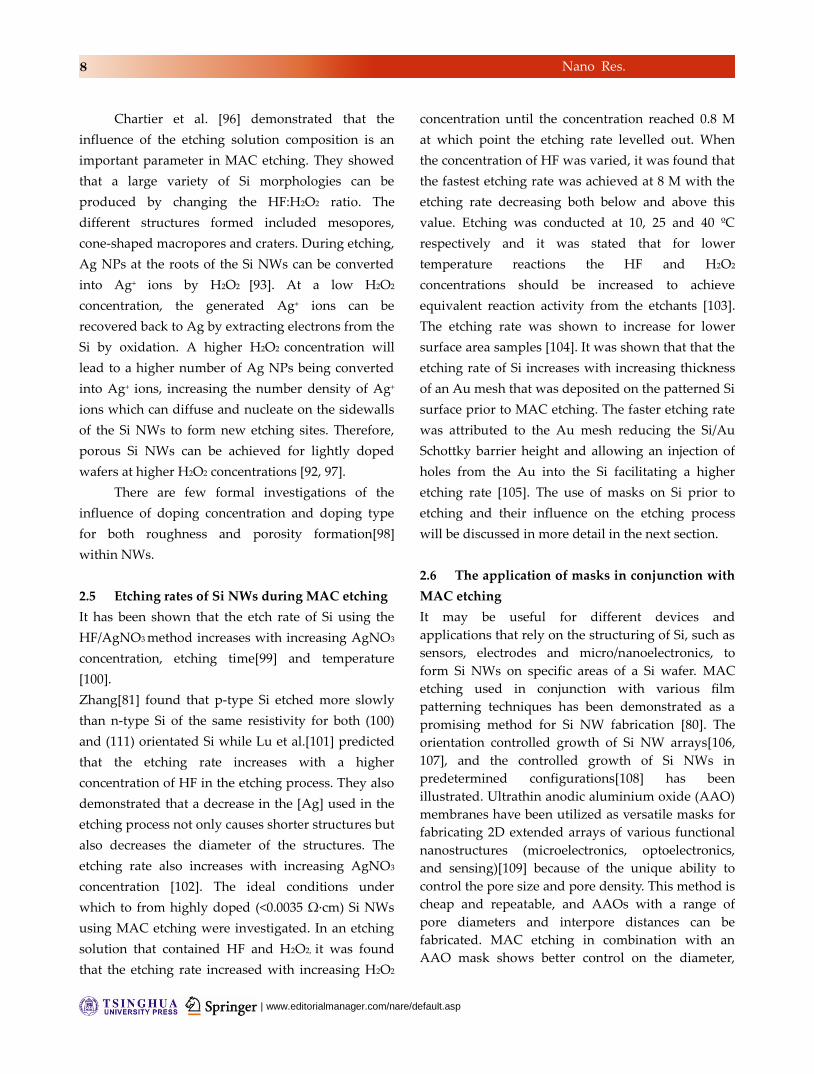
Figure 7(a) shows an SEM image of Si NWs
after selective etching in conjunction with an AAO
template. The dense array of Si NWs formed are
capped by Au particles on their top, which are
orientated vertically, perpendicular to the surface of
the Si(100) substrate. The average diameter of the
NWs is ~60 nm, corresponding to the pore size in the
AAO template [110].
An example of an AAO based procedure is
schematically illustrated in Fig. 7(b). First, an
ultrathin AAO membrane/polystyrene composite
was placed on a Si substrate (7(b(i))). Reactive ion
etching (RIE) was performed to pattern the surface of
Si (100) substrate under SF6/O2, followed by removal
of the ultrathin AAO mask (b(ii)). A thin layer of Ag
or Au was deposited onto the patterned Si (100)
substrate (b(iii)). Finally, arrays of vertically aligned
Si NWs on the Si (100) substrate were obtained by
performing MAC etching (b(iv)) [113].
| www.editorialmanager.com/nare/default.asp
10 Nano Res.
Figure 7 (a) Side-view SEM image with 60° tilt of Si NWs after
selective etching of the AAO template [110]. (b) Schematic of
the MAC etching process in conjunction with the use of a
photoresist mask [113].
Another method was developed to fabricate
high-density and well-aligned Si NWs through MAC
etching using metal nanodots as a hard mask [114].
By fine-tuning the pore size of the AAO template
used in the metal nanodot fabrication, the diameter
of Si NWs could be precisely controlled down to a
precision of 10 nm.
Huang et al.[115] studied the MAC etching
behavior of Si(110) substrates in conjunction with a
metal film deposited using an AAO mask and found
that the two preferred <100> etching directions can be
suppressed by the presence of a metal film. Vertical
or angled Si NWs relative to the substrate surface
could be formed depending on the morphology of
the film. [110] Si NWs were formed using this
process with the diameter of the Si NWs being
controlled by the pore diameter in the AAO template.
MAC etching of Si(100) substrate using a gold
mesh as catalyst was used to fabricate Si NWs with
varying orientations and morphologies, including
zigzag Si NWs, [111] Si NWs, and curved Si NWs
[116]. It was found that the crystal orientation and
morphology of Si NWs are controlled by the injection
of holes (h+) into the valence band of and removal of
oxidized Si by HF.
2.7 Orientation control of Si NWs using MAC
etching
The direction of Si NWs relative to the substrate
surface is important for Si NW based solar cells[117]
and Si NW based field effect transistors [90, 91].
Initially it was shown that etching in (100) and (111)
Si occurred in the vertical direction only [59, 118].
However, more recently, contradictory reports have
shown that the formation of slanted NWs from
substrates with these orientations [59, 80, 118-120].
Also, non-(100) substrates have shown preferential
etching in the (100) direction [59, 80, 118-120]. It was
found that for (100) wafers with resistivity of 6–8 Ω
cm, vertical (100) Si NWs were formed at a
volumetric ratio of 3:1 HF:H2O2 while (111) Si NWs
were generated when the HF concentration was
increased [91].
Chen et al.[121] prepared zigzag Si NWs with
different turning angles via a MAC etching approach.
This was made possible by controlling the spatial
concentration of Ag NPs during etching. The shapes
of the zigzag Si NWs could be controlled via the
orientation of the Si wafer, etching temperature, and
etchant concentration. The orientation of the Si NWs
produced could also be tuned by simply scratching
the surface of the Si wafer; it was shown that the
scratched area of the Si produced zig-zag Si NWs,
while the unscratched surface produced straight Si
NWs. A selection of these Si NWs are shown in Fig.
8(a-f). Variation of the etching direction in (111)
n-type Si has also been illustrated through changes in
the HF:AgNO3 ratio, etching temperature and time.
The etching direction of the Ag particles was shown
to be (111), (110), (211), (311) and zigzag depending
on the etching conditions as shown in Fig. 8(g-l)
[122].
Oxidation-rate-dependent etching was
observed in (111) and (110) Si substrates. In high
oxidant concentration solutions, the etching occurs
along the surface normal, but in low oxidant
solutions the etching occurs in the <100> directions.
Etching direction was also shown to change with a
change in current density [104].

www.theNanoResearch.com∣www.Springer.com/journal/12274 | Nano Research
11 Nano Res.
Figure 8(m-p) shows SEM images of Si NWs
fabricated from (100) and (111) Si wafers. As shown
in Fig. 8(m), Si NWs generated on Si(100) substrate
were perpendicular to the etched surface. However,
Si NWs formed from the Si(110) substrate were at an
angle to the Si substrate, as shown in Fig. 8(n) and
Fig. 8(o). The white arrows in Fig. 8(o) show the
preferential [100] orientation of the Si NWs. This
preferred etching direction is also shown in Fig. 8(p)
[120].
Tsujino et al.[123] showed that Ag particles etch
in the (100) direction through Si(100) in a solution
containing 5.3 M HF and 0.18 M H2O2 resulting in
vertical pores. When etched for longer it was shown
that there were also horizontal pores emanating in
the [0 1 0], [0 -1 0], [001] and [0 0 -1] directions which
are all crystallographically equivalent to the [100]
direction. When the H2O2 concentration was reduced
to 0.0018 M, the pores showed no preferred etching
direction indicating that the etching direction may be
related to the H2O2 concentration.
Vertically aligned zigzag Si NWs have been
produced by etching a p-type Si(100) substrate twice
[116]. The first etch was undertaken on a Si (100)
wafer with an Au mesh in a solution of HF:H2O2 ratio
of ~0.23 the second etch took place in a solution of
HF:H2O2 ratio of ~23. While the HF:H2O2 ratio
affected the morphology (porous NWs were formed
at a lower HF:H2O2 ratio while nonporous NWs were
formed at a higher ratio) of the Si NWs, the authors
stated that it had no bearing on the etching direction.
The etching temperature however did have an
influence on etching direction, as would be expected
from a high-rate generation and consumption of
carriers or fast kinetics.
It was found that the etching direction of a
given Si crystal orientation could be changed by
varying etching conditions [63]. The MAC etching
direction of Si(100) can be changed from <100> at
room temperature to <110> at a higher temperature
depending on the H2O2 concentration. When the
H2O2 concentration is ≤ 0.485 M, the etching always
proceeds along <100> direction but when the H2O2
concentration is increased to ≥ 0.727 M the etching
direction changes to <110> at a higher temperature.
The etching direction on Si(110) has also been
shown to be related upon the structure of the metal
film deposited on the surface. A 5 nm thick Ag film
that was characterised as being isolated patches with
irregular shapes yield slanted Si NWs, whereas a 10
nm Ag film with randomly distributed pores yielded
Si NWs perpendicular to the substrate [115]. Si(100)
was etched using a solution of HF and H2O2, while
the vast majority of the etching took place
perpendicular to the substrate surface, some etching
parallel to the substrate surface was observed [124].
The hypothesis presented was that non-spherical Ag
particles change etching course in the
crystallographically identical <100> direction.
To investigate the role of dopant type and
substrate orientation in determining the orientation
of MAC etching produced Si NWs, Zhang et al.[81]
etched p- and n-type Si(100) and p- and n-type Si(111)
wafers. Independent of the doping type, it was found
that both of the (100) wafers yielded NWs
perpendicular to the substrate. The p-type Si(111)
wafer yielded uniform Si NWs that were at an angle
of 40º to the substrate surface in the <100> direction.
The n-type Si(111) wafer resulted in NWs
perpendicular to the substrate and a TEM
investigation showed a (111) orientation for the NWs.
It was also shown that in Si(111), Au particles etched
at approximately 55º to the surface in (100) direction
[112].
Table 1 summarizes how the etching direction
in Si can be change by varying the etching
temperature, HF:H2O2 ratio and the HF:AgNO3 ratio.
Here, we have discussed MAC etching of Si
NWs and the processes that enable etching. The
advantages of MAC etching Si NWs in comparison
for Si NWs formed via other methods typically VLS
were discussed. Fundamentally, the doping level
dictates the energetics of the semiconductor-solution
interface and ultimately the rate of Li-ion insertion
into the anode. The doping profile determines the
depletion layer width, the relative redox
potential-Fermi level shift, the Helmholtz and other
double layer capacitances that influence ionic
diffusion rates to the surface, the flat-band potential
and the electron density at the surface required to
reduce Li+, among many other characteristics. Many
of these characteristics are ill-defined in
nanostructured silicon that is synthesized from
precursor or through other bottom up methods, an

| www.editorialmanager.com/nare/default.asp
12 Nano Res.
issue compounded by the lack of control of the
spatial density of active dopants within
nanostructures. Secondly, MAC etching and other
electrochemical etching protocols for silicon, and by
extension to Ge, may allow for phenomena such as
depletion layer capacitance control of charge transfer
not possible when nanoscale silicons are deposited
on metallic current collectors. These phenomena,
among others that influence reversible alloying with
lithium will be outlined in the next sections.
The importance of porous Si NWs and how
these porous Si NWs could be formed were
investigated, this was typically done through the
etching of highly doped Si but porous Si could also
be formed from low doped Si under the correct
etching conditions. The application of AAO masks,
block-co-polymer patterning and other methods in
conjunction with MAC etching to from Si NWs
demonstrated some advantages of MAC etching for
selective etching and site-specific NW growth. The
various etching directions in the varying Si wafers
orientations were discussed, typically the etching
direction is dependent on the wafer orientation but
again this can be overcome by varying the etching
parameters.
Figure 8 (a, b, and c) SEM images of three kinds of zigzag Si NW arrays on a Si wafer. TEM(d) and SEM(e,f) images of single zigzag
NWs. Inset are TEM images and electron diffraction patterns of the turning point of zigzag NWs showing their growth directions
alternating between (d)⟨111⟩ and ⟨113⟩, (e)⟨111⟩ and ⟨100⟩, and (f) two different ⟨100⟩ directions, respectively [121]. (g-l) Si NWs
formed from n-type Si(111), without (g) and with (h−l) solution stirring [122]. (m,n) Cross-sectional SEM images of Si NWs formed on
a Si(100) substrate(m) and a Si(110) substrate(n). (o) Top-view SEM image of Si NWs on a Si(110) substrate. Inset is the projection of
the Si NWs on the (110) plane. The orthogonal directions indicate the Si NWs oriented in the [100] directions. (p) SEM image showing
the branching pores on a Si(110) substrate [120].

www.theNanoResearch.com∣www.Springer.com/journal/12274 | Nano Research
13 Nano Res.
Reference Wafer
Orientation
Initial
etching
direction
Initial/Final
Temp
Initial/Final
HF:H2O2
ratio
Initial/Final
HF:AgNO3
ratio
Final
etching
direction
Chern[91] (100) <100> 2:1 / 3.5:1 <111>
“ (110) <100> 2:1 / 3.5:1 <111>
“ (111) <100> 2:1 / 3.5:1 <111>
Chen[121] (111) <111> 15 °C / 75 °C Zig-Zag
Bai[122] (111) <110> 2.5:1 / 50:1 <111>
“ (111) <211> 10 °C / 20 + ≥
30 °C
<311>
+<111>
“ (111) <111> 250:1 / 50:1 Zig-Zag
Huang[104] (111) <111> 46:1 / 2300:1 <100>
“ (110) <100> 11.5:1 / 4.6:1 <110>
Table 1: A summary of how the etching direction in Si wafers can change with varying HF ratios and etching temperatures.
3 Si anodes for Li-ion batteries
Rechargeable LIBs are prevailing as the power
source of choice for portable electronics and hybrid
electrical vehicles [3, 125-128]. For mobile
applications, high energy (per weight and volume)
is the most important parameter since it determines
the usage time per charge [129]. Compared to other
technologies, LIBs have high energy densities, good
cycle life, and good power performance [1, 3, 125,
126, 130, 131]. LIB performance involves
inter-related electrochemistry, phase transitions and
transport processes at the interfaces between
electrodes and electrolytes [132].
To improve the performance of LIBs,
improved understanding of the behaviour of active
materials is sought. Bulk Li alloy type anodes
comprising of elemental Sn, Al, Ge, Si or their alloys
showed their functionality as LIB anodes with large
specific and volumetric capacities [133]. Li would
be the most favourable anode material for LIBs in
terms of specific energy and electrode potential but
safety problems and loss of capacity upon cycling
have prevented this [3, 134].
Si is an attractive anode material for LIBs
because it has a relatively low potential range at
which charge occurs, below 0.5 V[135] when
reacting with Li. Si is known to incorporate a
theoretical maximum of 4.4 Li atoms per Si
atom[135], resulting in the highest known
theoretical charge capacity (~4,200 mAh g-1)[136]
which is more than ten times higher than the
capacity of conventionally used graphite (~372
mAh g-1) and much higher than alternative oxide
materials [54, 80, 119, 122, 137-140]. The discharge
curve of Si during the electrochemical extraction of
Li is relatively flat, very similar to that of graphite,
allowing a constant energy and power delivery. In
addition to its high capacity, Si is the second most
abundant element in the Earth’s crust, is
environmentally friendly and is the focus of many

| www.editorialmanager.com/nare/default.asp
14 Nano Res.
worldwide corporations, which also makes it
attractive when considering its use as an anode in
LIBs. Rolled-up batteries based on Si NWs have
even been demonstrated from silicon used in chips
[141]. Li15Si4 is the highest lithiated phase achievable
for the ambient temperature lithiation of bulk Si
and corresponds to a capacity of 3579 mAh g-1 [142].
When bulk Si is fully lithiated to Li15Si4 it undergoes
a volume expansion of 280% and has a maximum
theoretical volumetric capacity of 2190 mAh cm-3.
Unfortunately, Si electrodes pulverize due to the
large expansion and contraction upon Li insertion
and extraction and this causes the electrode
material to lose contact with the current collector,
lower its conductivity, and result in a loss of
capacity with cycling [71, 95, 133, 143-148]. Several
Si structures have been investigated as viable
anodes for LIBs, including Si thin films [149, 150]
and Si powder [151, 152].
Recent work involving in situ TEM
measurements of the crystalline to amorphous
transition in silicon/Li-Si nanoparticles during
reversible charge-discharge cycling suggested a
critical size of ~150 nm for crystalline silicon[153]
and a size of 870 nm for amorphous silicon[154],
beyond which particles develop cracking and
structural degradation to the point where the
material breaks up. When considering realistic
anode compositions, comprising densely packed
nanoparticle and structures, the critical sizes for
lithiation/delithiation induced break-up might be
different and postulated to be smaller due to
nearest neighbour interactions [155]. However,
electrolyte access to all particles is an assumption
that is not strictly proven, and the influence of the
crystal facet (known to strongly influence the
insertion rate capability of Li ions into silicon for
example), was not considered. These influences
must also consider the relative changes in electrical
conductivity of the networked nanomaterial in
silicon anodes designed to overcome adverse effects
of volumetric changes on structures that are not
perfectly spherical.
Recent theoretical investigations of the
lithiation/delithiation mechanism in silicon, in
parallel with experimental investigations of
multistep amorphization of this Li-Si alloy phases,
have suggested that porous structured silicon with
nanoscale pores or other constructs with defined
voids provide additional free space for volume
expansion induced by lithium-ion
insertion[156-159]. While this concept is somewhat
obvious, the type, degree and form of the porosity
can influence the response to volumetric changes in
some cases, which is influence by orientation of the
crystal facets and by the nanoscale structure [157].
Some authors have demonstrated, through
analytical modelling, that the effect of stresses and
strains caused by insertion and extraction
(dealloying in the case of silicon) reactions is
dynamic, i.e. that the material, once lithiated, is no
longer a simple crystalline silicon as modelled from
the outset. Stresses and strains in Li-Si phases that
undergo various amorphization processes during
insertion and removal of lithium compound that
changes in structure and also the original porosity
designed to alleviate the expansion/contraction
issue. Furthermore, significantly more effort is
needed to consolidate all these effects with the
variation in the rate of insertion and extraction at
different facets, mediated by various doping levels,
and the change in electronic band structure of Li-Si
versus Si phases and their degree of crystallinity.
3.1 Si thin film behavior as a Li-ion battery anode
Thin films of Si may be more robust than bulk Si over
repeated cycles of Li insertion and extraction owing
to their thin, uniform nature. As a result, many
studies have examined their use as LIB anodes.
Importantly, when developing further understanding
of the reversible lithiation behaviour of nanoscale
silicon and related materials with better physical
properties (those from etching top-down rather than

www.theNanoResearch.com∣www.Springer.com/journal/12274 | Nano Research
15 Nano Res.
grown bottom-up) including metal-metalloid
composites (Si-Sn, etc.), the response known for bulk
scale single crystals, thin films, amorphous and
compositionally graded silicon in LIBs is important
to overview in context. Ohara et al.[160]
vacuum-deposited Si films onto Ni foil. The Si film
was expected to stick tightly to the Ni film even after
volume expansion and contraction due to Li insertion
and removal. The Si thin film retained its initial cyclic
voltammetry (CV) curve for 500 cycles and a capacity
of ~1000 mAh g-1 after 1000 cycles represents
impressive cycling by the anode. They found that
high rate deposition of the Si on the Ni foil was a
factor in rapid capacity deterioration with cycling,
while deposition that was defined as being too slow
caused the Si to be inert to rapid Li insertion.
Amorphous Si thin films of 250 nm and 1 μm
thickness respectively were sputter-deposited on Cu
foil [145]. The reversible capacity of the 250 nm film
was found to be ~3800 mAh g-1 with a fade of 0.09%
per cycle when cycled at a current density of ~C/2.5
while the reversible capacity of the 1 μm film was
~3000 mAh g-1 with a capacity fade of 0.2% per cycle
when cycled at the same current density. This shows
that thinner Si films exhibit enhanced cycling ability
in comparison to thicker Si films.
Unfortunately, this capacity retention was only
maintained for ~20 cycles for the 1 μm thick film and
~30 cycles for the 250 nm thick film as can be seen in
Fig. 9(a). A possible reason for the decrease in
capacity is the pulverization of the Si thin film, with
cracking reducing electrical contacting to both the
current collectors and the active material in-plane.
When the active material is pulverized due to the
expansion and contraction taking place in its crystal
structure, the material can lose electrical contact with
the current collector and hence reduce the capacity of
the electrode by rendering some of the active
material electrically (and thus electrochemically)
inactive for charge storage. The cracking of the Si
anode can be seen in Fig. 9(b,c) [145]. This is typical
for a non-nanostructured alloy type material reacting
with Li. The cracking of the Si anode can be visually
compared to the cracking of most brittle porous
materials. This effect was also shown in other Si thin
films[146] and also in tin (Sn) alloys [133].
Figure 9 (a) Comparison of galvanostatic cycling of 250 nm and
1 μm Si films on Cu foils (both at ~C/2.5 rate). Plan-view SEM
image of 250 nm Si film cycled at ~ C/2.5 for (b) 1 cycle and (c)
30 cycles [145].
Si thin films have also been prepared by
chemical vapour deposition (CVD). It was shown
that an amorphous Si thin film could be cycled with a
maximum discharge capacity of ~4,000 mAh g-1, but
that the capacity faded rapidly after 20 cycles.
However, by increasing the lower potential limit
from 0 V to 0.2 V and therefore limiting Li insertion,
the capacity of the electrode was reduced to 400 mAh
g-1 but the electrode retained this capacity for ~400
cycles [149].
Using a similar method, Si was vacuum
deposited onto Ni foils by Uehara et al[161],
Takamura et al.[162], and Ohara et al.[150]. It was
found that thinner Si films retained capacity better
than thicker Si films, that roughening the Ni foil
improved capacity and that capacity of the Si films
decreased with an increasing C-rate. Si films have
also been deposited on different substrates including
graphene foam (via CVD), with the resulting anode
achieving a reversible capacity of 1.4 mAh cm-2. The
authors claimed that the graphene foam provided a
conductive pathway for charge transport and
facilitated the expansion of the Si upon charging
[163].
Zhao et al.[164] also electrodeposited a Si film
on a Ni foam. The film showed an initial capacity of ~

| www.editorialmanager.com/nare/default.asp
16 Nano Res.
4830 mAh g-1 which quickly decreased and plateaued
at 2800 mAh g-1 for 80 cycles with a Coulombic
efficiency (CE) of >95 % after the first cycle. For
comparison, pristine Si NPs were also tested. The Si
film exhibits much better performance than Si NPs,
whose capacity fades quickly. From electrochemical
impedance measurements, the diffusion coefficients
of Li+ in pristine Si NPs were found to be much
slower than that of the Si film after the first cycle.
This helps explain the improved performance of the
Si film vs the NPs.
3.2 Si combined with other elements to form an
anode
Composite Si electrodes were investigated and were
shown to improve the capacity retention vs pure Si
anodes. The additional elements often act as a buffer
(preventing Si expansion) or as a conductive additive
(increasing the conductivity of the anode). In this
section we look at how these elements were
incorporated.
A layered microporous Cu/Si/Cu electrode was
fabricated and coated with Polyethylene (PE) to
stabilize the electrode during Li insertion. A
schematic of this electrode is shown in Fig. 10(a)
[165]. This electrode retained a capacity of > 1000
mAh g-1 for over 120 cycles while retaining its pore
structure. With the top and bottom Si surfaces
blocked by Cu, Li insertion into Si primarily occurred
at the Si sidewalls. It is believed that this led to a
more uniform lithiation of the Cu/Si/Cu electrodes
and hence resulted in the anode retaining its
structure. A porous Si/Cu film was also investigated,
the porous nature of the anode allowed it to expand
and contract without pulverization, the lack of
pulverization aids in the capacity retention of the
anode and it exhibited a capacity of 1628 mA h g-1
after 100 cycles [104]. This report exhibits the
importance of potentially limiting Li insertion into Si
anodes.
Hatchard et al. [166] produced SiAlSn films by
combinatorial sputtering. They attained capacities of
up to 1800 mAh g-1, as well as reversible capacities of
over 1500 mAh g-1 when cycled between 1.2 and 0.1 V
vs. Li for 10 cycles. They showed that capacity
retention was best in amorphous areas of the film,
while the capacity faded quickly when there was
crystalline material present due to the
inhomogeneous nature of the expansion and
contraction of the crystalline material.
Si has also been used in combination with other
alloying materials in dually active composites. Si and
Ge layers were deposited in sequence on a Cu
current collector, with the number of layers being
varied with the resulting structures electrochemically
tested as anodes. A single Si/Ge layered electrode
was fabricated with each layer being 0.65 µm thick,
while more complex layered Si/Ge electrodes (10
layers with each layer being 65 nm thick and 100
layers with each layer being 6.5 nm thick) were also
fabricated as shown in Fig. 10(b-e). Figure 10(b-d) are
SEM images of these three electrodes showing the
alternating layers. Figure 10(e) is a TEM image of the
100 layer electrode showing the thickness of the
alternating Si and Ge layers. After 100 cycles, the 10
layer Si/Ge electrode had a capacity of ~1000 mAh g-1,
while the 100 layer and mono layer Si/Ge electrodes
both had capacities ~500 mAh g-1. It was proposed
that the Ge acted as a buffer to volume change
during Li insertion and extraction. However it was
noted that the performance for the 100 layer
electrode decreased since the film could not endure
the plastic deformation due to that electrode having
the highest expansion/contraction rate of the three
electrodes [167].
While the anodes do not achieve their
theoretical maximum capacity, the limiting of Li
insertion would lead to a better cycling performance
of the Si anodes. The additional elements also help to
prevent the full expansion of the Si hence reducing
the degradation of the anode. The additional
elements also improve the conductivity of the Si
anodes.
3.3 Si powder anodes
Si electrodes with Si powders were prepared and had
partial success in alleviating the volume change
associated with Li insertion and extraction [168-170].
Si powders were also fabricated as composites to
improve the conductivity to improve capacity
retention with cycling [171-177].

www.theNanoResearch.com∣www.Springer.com/journal/12274 | Nano Research
17 Nano Res.
Figure 10 The schematic shown in (a) depicts the encapsulated
microporous device, Cu/Si/Cu. [165] (b)–(e) SEM cross sectional
images. Si and Ge were alternately deposited (b) one time, (c) ten
times and (d) 100 times on a Cu current collector. (e) TEM image
of the 100-layer electrode [167].
Electroless deposition of Cu has been used to
enhance the electrical conductivity of Si powder [178].
The Si was etched before the Cu deposition. The
resulting Cu-deposited Si powder electrodes
exhibited improved cycleability compared to bare Si
anodes. For different samples, which had different
electrical conductivities, the first discharge capacity
was larger and the capacity retention improved with
an increase in the conductivity of Si powders.
Kim et al.[179] investigated the formation of
C-coated Si/graphite powders as anode materials. A
TEM image of C-coated Si powder is shown in Fig.
11(a). This anode showed a high reversible capacity
of over 600 mAh g-1 for 15 cycles. They compared a C
coated Si/graphite anode and a pristine Si/graphite
anode and although an initial discharge capacity of
750 mAh g-1 could be obtained for the two anodes,
the C-coated Si/graphite composite anode showed
better cycling performance compared with pristine
Si/graphite anode as shown in Fig. 11(b). It was also
shown that reducing the Si particle size improved the
capacity retention of the Si anode.
In a similar approach, a 3D C-coated porous Si
(PS) powder was fabricated [180]. The CV response
of the C-coated Si exhibited higher currents than that
of the raw Si indicating a much larger surface area
for electrochemical reaction. The raw nonporous Si
had an initial capacity of >3000 mAh g-1 but this fell
quickly to ~250 mAh g-1 after 10 cycles. The C-coated
Si also exhibited an initial capacity of >3000 mAh g-1
however the capacity after 10 cycles was ~1500 mAh
g-1 and after 100 cycles the capacity was shown to be
~665 mAh g-1. The improvement in capacity retention
was ascribed to a shorter Li+ diffusion length in the
porous powder and a greater surface area when
compared to the raw Si.
The failure modes of Si powder as an anode
were investigated by Ryu et al.[152] It was found that
capacity fading occurs primarily in the delithiation
stage. The electrodes showed a marked increase in
resistance during the delithiation process due to loss
of contact between the Si and C in the anode which
prevented complete delithiation. Si anodes then
degraded with Li ions still remaining within the
anode structure because delithiation was not
completed for each cycle.
Si powders were investigated as anodes for
LIBs an it was shown that the addition of other
elements (Cu), the incorporation of conductive
additives (C) and the formation of porous Si powder
all improved the capacity retention of the Si anodes.
These results show the importance of additives into
the Si anodes.
3.4 The influence of doping and conductivity on
the performance of Si anodes
There is limited information in the literature
concerning the influence of Si crystal orientation,
carrier concentration and dopant type on Li insertion
and extraction processes. An important characteristic
of Si is its doping density, which is directly related via
its carrier mobility, to its conductivity. The
conductivity of Si anodes is typically varied by
introducing a conductive additive (often a

| www.editorialmanager.com/nare/default.asp
18 Nano Res.
carbon)[181-184], which are often required for
intrinsically doped or materials and structures with
low conductivities [185].
Figure 11 (a) TEM image of C coated Si powder and (b) the
cycle performance of a C coated Si/graphite electrode vs an
uncoated Si/graphite electrode [179].
The few studies that do exist on the lithiation of
doped Si in nanostructured form are as dispersed
powder mixtures, often involving amorphous Si[186]
or polycrystalline nano Si-graphite mixtures[187] and
related nanoscale Si analogues. The doping
contribution to conductivity and Li uptake (reduction
of Li upon insertion at the cost of an electron) is
difficult to separate from enhanced electrical
conductivity of the entire material matrix, which
becomes continually hole-doped while changing its
structure, composition and electrical nature. This is
further complicated by changes in active material
contacts within the matrix, the random, uneven
distribution of conductive additives in powder
materials, and the inconsistency in rational doping of
some forms of Si.
Doping type and density modify the Li
insertion and extraction processes, and in nanoscale
systems all of the abovementioned parameters,
including doping control, can vary from
nanostructure to nanostructure [188]. Etching of bulk
wafers is one method to improve doping control,
orientation and electrical contact. Peng et al.[78] and
Flake et al.[189, 190] reported Si NW anodes
fabricated by MAC etching of Si wafers. This method
has the potential for precise control of the doping of
the NWs [78, 191, 192]. Density functional theory and
related modelling have confirmed a crystal
orientation influence on Li insertion in a variety of
materials[193], leading to prediction of cell potentials,
favoured higher rate insertion facets, and links
between the Li uptake and the crystallographic phase
change. Amorphization, morphology changes and
secondary electrolyte interphases can occur during
reversible lithiation. A first principles study suggests
that dopants can have an effect on the binding energy
of Li with Si [194]. A systematic examination of
doping on many aspects of Li insertion and removal
in Si is still required.
Long et al.[195] showed the effects of Boron (B)
and Phosphorus (P) dopants on the lithiation of
crystalline Si. By using Raman scattering
spectroscopy, they were able to identify differences in
Li insertion potentials for the different dopant types.
The B dopant moves the lithiation potential higher
relative to the undoped Si, whereas the P dopant
lowers the insertion potential as shown in Fig.
12(a+b). The different Fermi levels in heavily B- and
P-doped surfaces affect Li insertion energetics by
respectively lowering and raising the energies of
states available to the electron accompanying the Li+.
This explains the higher initial Li insertion potential
for the p-type Si when compared to n-type Si. The Li
insertion energy as a function of Li depth is shown in
Fig. 12(c) for both doped and undoped Si, with
different orientations and with H passivation.
Surface lithiation on both p-type and n-type Si
surfaces is energetically favourable, whereas Li
insertion below the surface (depth >0) is favourable
only on p-type Si surfaces. For subsurface lithiation
of n-type Si surfaces, dilute Li insertion into the
subsurface is not possible, but higher Li-content
silicides may be formed. In contrast, initial Li
insertion into the subsurface layers of p-type Si
surfaces occurs at 0.5-1 V. Therefore, Fig. 12(c)

www.theNanoResearch.com∣www.Springer.com/journal/12274 | Nano Research
19 Nano Res.
provides an explanation for the observation that Li
insertion into a p-type Si surface occurs at a higher
voltage than into the corresponding n-type Si surface.
B-doped Si particles were prepared by
high-energy ball-milling of B and Si powders in
varying ratios [196]. The two electrodes were
prepared with the following nominal B
concentrations (atom per mole Si): 0 and 1021,
(equivalent to 0 and 0.167 at.% B, respectively). The
B21 anode was shown to be less resistive than the B0
anode, but contrary to other reports it was shown
here that the doping has little to no difference in the
electrochemical performances of the two anodes. It
was stated that the high relative resistance of Si does
not play a key role in the poor electrochemical
performance of Si-based electrodes.
In a study examining the impact of n-type
doping on electrochemical performance, intrinsic Si
thin films and n-type conductive Si thin films
deposited on Ni current collectors were compared
electrochemically [150]. It was shown that not only
the specific capacity but also the cycle performance
of the conductive Si were much improved when
compared with those of the intrinsic Si film. The
initial charge/discharge efficiency was improved
from 65% to 88%. It was concluded that the electrical
conductivity of the deposited film plays an important
role in providing a favourable performance for the Li
insertion/extraction reaction.
Separate investigations on the influence of
doping levels and doping type (where the majority
charge carriers are holes rather than electrons for Li
reduction), have shown that different conduction
type silicon (n- or p-type) can influence the degree to
which Li is intercalated and the associated
mechanism of amorphization. Raman scattering
mapping X-ray photo-electron spectroscopy of n- and
p-type silicon after lithiation conclusively showed
that highly doped n-type Si(100) surface regions
retain Li as a silicide and convert to an amorphous
phase during early cycles via a polycrystalline phase
as a two-step phase conversion process[197].
While doping of Si influences the resistivity
and the Li insertion potentials of the Si anodes, some
confusion remains as to whether or not the doping of
Si has a role to play in the improvement of the
capacity and capacity retention of Si anodes.
Figure 12 CVs of (a) Si(100) n-type and (b) Si(100) p-type. (c)
Single Li insertion energy relative to bulk Li for B- and P-doped
Si (100) and (111) surfaces. For the (100) surface, results with
hydrogen passivation on the top surface are also shown [195].
3.5 Composites of silicon
Pure Si anodes exhibit poor cyclability due to the
stresses in the Si caused by large volume changes
upon Li insertion and removal. One method to
overcome this is to place the active Si material within
a “buffering” inactive material. The inactive material
would not contribute to the capacity of the anode but
it would however prevent the Si anode from
expanding fully and hence improve the cyclability of
the anode. These types of Si anodes are often called
composite anodes as they often contain two or more
different elements.
A composite electrode architecture, a
(Ba–Fe–Si/C composite) was synthesized by
mechanical ball milling [180]. It was shown that the
Ba–Fe–Si/C composite not only possessed a reversible
capacity of 420 mAh g-1, but also exhibited very
stable capacity retention with very little capacity
decay after 25 cycles. The Ba-Fe-Si/C composite also
retained capacity better than a pure Si anode and a
Ba-Fe-Si alloy despite having a lower initial capacity
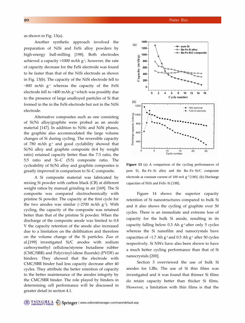
| www.editorialmanager.com/nare/default.asp
20 Nano Res.
as shown in Fig. 13(a).
Another synthetic approach involved the
preparation of NiSi and FeSi alloy powders by
high-energy ball-milling [198]. Both electrodes
achieved a capacity >1000 mAh g-1, however, the rate
of capacity decrease for the FeSi electrode was found
to be faster than that of the NiSi electrode as shown
in Fig. 13(b). The capacity of the NiSi electrode fell to
~800 mAh g-1 whereas the capacity of the FeSi
electrode fell to <400 mAh g-1 which was possibly due
to the presence of large unalloyed particles of Si that
formed in the in the FeSi electrode but not in the NiSi
electrode.
Alternative composites such as one consisting
of Si/Ni alloy/graphite were probed as an anode
material [147]. In addition to NiSi2 and NiSi phases,
the graphite also accommodated the large volume
changes of Si during cycling. The reversible capacity
of 780 mAh g-1 and good cyclability showed that
Si/Ni alloy and graphite composite (6:4 by weight
ratio) retained capacity better than the 7:3 ratio, the
5:5 ratio and Si–C (5:5) composite ratio. The
cycleability of Si/Ni alloy and graphite composites is
greatly improved in comparison to Si–C composite.
A Si composite material was fabricated by
mixing Si powder with carbon black (CB) at different
weight ratios by manual grinding in air [169]. The Si
composite was compared electrochemically with
pristine Si powder. The capacity at the first cycle for
the two anodes was similar (~2700 mAh g-1). With
cycling, the capacity of the composite was retained
better than that of the pristine Si powder. When the
discharge of the composite anode was limited to 0.8
V the capacity retention of the anode also increased
due to a limitation on the delithiation and therefore
on the volume change of the Si particles. Zuo et
al.[199] investigated Si/C anodes with sodium
carboxymethyl cellulose/styrene butadiene rubber
(CMC/SBR) and Poly(vinyl-idene fluoride) (PVDF) as
binders. They showed that the electrode with
CMC/SBR binder had less capacity decrease after 40
cycles. They attribute the better retention of capacity
to the better maintenance of the anodes integrity by
the CMC/SBR binder. The role played by binders in
determining cell performance will be discussed in
greater detail in section 4.1.
Figure 13 (a) A comparison of the cycling performances of
pure Si, Ba–Fe–Si alloy and the Ba–Fe–Si/C composite
electrode at constant current of 100 mA g-1 [180]. (b) Discharge
capacities of NiSi and FeSi–Si [198].
Figure 14 shows the superior capacity
retention of Si nanostructures compared to bulk Si
and it also shows the cycling of graphite over 50
cycles. There is an immediate and extreme loss of
capacity for the bulk Si anode, resulting in its
capacity falling below 0.3 Ah g-1 after only 5 cycles
whereas the Si nanofilm and nanocrystals have
capacities of ~1.7 Ah g-1 and 0.5 Ah g-1 after 50 cycles
respectively. Si NWs have also been shown to have
a much better cycling performance than that of Si
nanocrystals [200].
Section 3 overviewed the use of bulk Si
anodes for LIBs. The use of Si thin films was
investigated and it was found that thinner Si films
do retain capacity better than thicker Si films.
However, a limitation with thin films is that the

www.theNanoResearch.com∣www.Springer.com/journal/12274 | Nano Research
21 Nano Res.
film thickness is usually a few hundred nanometres,
which leads to a limited specific charge capacity of
~0.1 mAh cm-2 and is insufficient for viable
applications [201]. Amorphous Si was found to
exhibit superior cycling capability than crystalline
Si. The addition of other elements was found to
improve the capacity retention of Si anodes, either
by acting as a buffer to alleviate stresses during
expansion or to improve the conductivity of the
anode. The doping profile of Si anodes is also
shown to be one method to influence the Li
insertion potential into Si anodes but there are
contradictory reports of whether or not the doping
of Si anodes improves their performance as a LIB
anode.
Figure 14 The capacity of Si nanocrystals and a Si nanofilm
over 50 cycles. The theoretical specific capacity of graphite and
the measured capacities for bulk Si are also included [200].
Si nanostructures are now well know to cycle
much better than bulk Si, but the comparison is
often too limited in the literature. Affecting the
ambipolar conductivity for ions and electrons is a
primary motivator for choosing lower dimensional
silicon, but its affects the conductivity, doping
profile and the surface reactivity. Comparing bulk
to nanoscale silicon should ideally involve the
many aspects of the silicon-electrolyte interface that
go beyond simple size reduction effects, and form a
basis set for examining the many benefits, and
limitations, that nanoscale Li-ion battery materials
made from semiconductors possess. The knowledge,
even at bulk scale, of the influence of Si-metal
composites on the capacity, structural changes, Li
insertion and alloying metallurgy, and charge rate
variation among other characteristics is important
when making direct comparison to, and predictions
of, nanoscale silicon composite materials as LIB
anodes. The next section will deal with a variety of
shapes, sizes, crystal structures and composite Si
nanostructures as anodes in LIBs.
4 Nanostructured Si as anodes for Li-ion
batteries
This section focuses on a wide range of Si
nanostructures such Si NWs, Si nanopowders and
core-shell nanostructures as anode materials for LIBs.
In addition, the influence of doping and conductive
additives on their performance will be discussed.
Various Si nanostructures have been investigated as
viable anode materials for LIBs, including Si
nanopillars[202], Si NWs[203-205], Si nanowall
structures formed via lithography[206], core-shell Si
NWs[207, 208], Si inverse opal structures[113], Si
spheres[209], Si nanotubes[210], Si NPs[184],
pomegranate-inspired Si nanostructures[211] and Si
NWs decorated with Si NPs [212]. Considerable
progress has been made regarding nano-structured
Si as an active (insertion) and passive (scaffold)
anode material [72, 213, 214] and the viability of the
approach looks promising[215]. Laboratory scale
results obtained so far indicate that nano-structured
Si might meet the majority of battery requirements;
the ubiquitous supply of high quality bulk and
nanoscale silicons and the need for greener,
recyclable batteries will promote its development.
Recent investigations have focused on the quality
and development of ordered nanoscale wire and
pores arrays in Si for use in LIBs [196, 216].
The advantage of Si nanostructures over bulk

| www.editorialmanager.com/nare/default.asp
22 Nano Res.
Si material is that low-dimensional nanostructures
can accommodate the >400% volume change upon Li+
insertion and extraction in Si without pulverization
(Fig. 15(a)). They also provide good electronic contact
and conduction and display short Li+ insertion
distances. The nanostructures also have a higher
surface area accessible to the electrolyte, which
allows more of the electrolyte to react with the
electrode hence increasing capacity, but sometimes at
the expense of a greater fraction of charge associated
with stable solid electrolyte interface (SEI) formation
on a greater surface area. Figure 15(b) shows the
improved capacity of Si NWs over Si nanocrystals
and graphite over 10 cycles and Fig. 15(c-f) examines
Si NWs during the first Li insertion via TEM and
electron diffraction showing the transition from
crystalline Si to amorphous Si.
That Si NW structured anode showed great
promise as an anode for LIB as it attained the
theoretical capacity of Li in Si (~4200 mAh g-1) and
showed a 75% capacity retention over the first 10
cycles. This was one of the first example of Si NWs
being utilized a LIB anode and possibly stimulated
the research area of Si nanostructures as LIB
anodes.
Figure 15. (a) Schematic of the cycling behaviour of bulk Si, Si particles and Si NWs. (b) Capacity versus cycle number for Si NWs
at the C/20 rate. The charge data for Si nanocrystals (triangles) from[200] and the theoretical capacity for lithiated graphite (dashed
line) are shown as a comparison to show the improvement in capacity when using Si NWs.(c-f) Show the transition of a crystalline Si
NW(c) to an amorphous Si NW(f) via TEM and electron diffraction when the NW was charged to 10 mV [71].
4.1 Si nanopowder anode materials
One problem with Si NW electrodes grown via
CVD is the relatively low mass loading. A
Si-NP-decorated Si NW network was fabricated
[212] to investigate ways of increasing active mass
loading of silicon. The Si NPs were electrically
connected to Si NWs to increase the mass loading of
the Si NW electrode and a thin layer of Si deposited
by a CVD method overcoats the entire network to
ensure the excellent electrical conduction between
Si NPs and Si NWs, along with the stainless steel
substrates as shown in Fig. 16(a). It was shown that

www.theNanoResearch.com∣www.Springer.com/journal/12274 | Nano Research
23 Nano Res.
this process increased the areal capacity of Si NW
based electrodes, from ~0.6 mAh cm-2 to ~2.5 mAh
cm-2. The anodes showed good cycling performance
and maintained the decorated, porous network
structures after charging–discharging cycles.
Binders are essential for composite anodes by
providing adhesion between the anode materials
and current collectors. Generally, the adhesion that
the binder provides keeps the particles together in
the particle-based anodes and makes them adhere
to the current collector. Some methods involve
precursor synthesis of silicon containing
phosphazenes allow nanostructured powder
formation on conducting substrates directly,
including conductive carbon additive formation
through polymer decomposition [217, 218]. This is
particularly important in Si anodes which expand
and contract by >400% upon insertion and
extraction of Li+ ions.
Wagner[219] proposed the use of binders that
should be able to stabilize the electrode composite
during cycling. He proposed that the key
requirements of a binder are:
good binding properties
no extensive swelling in polar organic
electrolytes
electrochemical stability
processability
Wu et al.[220] created an electrode by mixing
nanosized Si, micrometer sized Si and using
poly(9,9-dioctylfluoreneco-fluorenone-co-methylbe
nzoic ester) (PFM) as a binder. The electrode
retained a capacity of ~2500 mAh g-1 after 30 cycles,
which is a marked improvement on the electrode
where they used acetylene black in place of the
nano Si. They attribute the improved performance
(both in terms of initial capacity and capacity
retention) to the ability of the nano Si to prevent
severe agglomeration of the micro Si which led to a
significant reduction of the stress induced by large
volume change of the macro-Si during the Li
insertion/extraction process. C-rate experiments
were also carried out on the electrode with the C/25
rate exhibiting a capacity of ~3000 mAh g-1 and the
2C rate exhibiting a capacity of ~2200 mAh g-1. The
key role played by binders in determining the
performance of LIB anodes based on Si particles
was shown by using a binder consisting of
β-cyclodextrin (or β-CDp). When examined as a
binder for Si anodes, the β-CDp was found to have
a self-healing effect where even Si particles that lost
contact with the anode could be recovered by the
binder. These particles could then contribute to the
capacity of the anode again [221].
A core-shell structured nano-Si/C electrode
was fabricated using Si nano-powder core and an
amorphous C shell [222]. This electrode was
compared to nano-Si/PVA electrode with PVA
acting as a binder. The initial charge capacity was
2300 mAh g-1 for the core-shell anode compared to
1200 mAh g-1 for the PVA anode. Four electrodes
were cycled for 50 cycles: nano-Si, nano-Si with
PVA, nano-Si with a C shell, and micron sized Si
with a C shell. After the 50 cycles the nano-Si with
the C shell electrode had a capacity of ~1500 mAh
g-1, whereas the other three electrodes had
capacities <500 mAh g-1 as shown in Fig. 16(b). This
shows the importance of the C shell and the size of
the Si particles to the performance of the electrode.
The behaviour of core-shell structures will be dealt
with in a later section.
Kuksenko et al.[223] stated that a reduction in
the size of Si, with transition to the nano-scale,
improves the structural strength of Si electrodes
against cracking upon large changes in volume, due
to lithiation and delithiation of Si anodes and hence
fabricated hybrid electrodes using two different
synthetic graphites (KS6 and MAG) and Si
nanopowder and three different binders. The
KS6/nano-Si/PVDF electrode exhibited an initial
discharge capacity of 930 mAh g-1 whereas the
initial discharge capacity for the
MAG/nano-Si/((sodium carboxymethyl-cellulose,
butadiene-styrene) Na-CMC,BSC) electrode was 354

| www.editorialmanager.com/nare/default.asp
24 Nano Res.
mAh g-1. This study shows how the use of different
carbons and binders can greatly influence the
performance of the Si anodes. In a similar approach,
a flake graphite/Si/C composite anode was
prepared [224]. The initial capacity was shown to be
~850 mAh g-1 which decreased to 552 mAh g-1 after
the 20th cycle. The initial capacity was much lower
than that of a raw nano-Si electrode (~3250 mAh g-1)
however the capacity of the raw Si electrode fell to
~160 mAh g-1 after 20 cycles showing the
importance of the inclusion of graphite and C in the
Si anode. A comparison the electrochemical
performance of various graphite/C/Si anodes is
shown in Fig. 16(c).
4.2 Methods of fabricating Si NWs:
vapour-liquid-solid growth
The VLS growth mechanism [69, 70] is a
well-known process for growing NWs that exploits
the eutectic region in a binary phase diagram. One
of the elements acts as a catalyst for nucleating the
NWs while the other is supplied as a vapour and
ultimately forms a solid NW. After the growth, each
NW has the catalyst as its tip. For Si, a common
catalyst is gold (Au); the Au catalyst is heated above
the eutectic temperature (363 °C) and SiH4 is
introduced and allowed to decompose into Si. The
Si dissolves in the Au particle and forms a eutectic
droplet. Upon reaching supersaturation, nucleation
of a single-crystalline Si NW occurs. Continuous
supply of Si vapour results in continued axial
growth of the NW[225] as is shown in the schematic
in Fig. 17(a). This alloying process can be depicted
as an isothermal line in a phase diagram (Fig. 17(b)).
SEM (c + d) and TEM (e, f) images of VLS grown Si
NWs on a stainless steel substrate are shown in Fig.
17(c-f). The VLS growth mechanism is a versatile
synthetic approach which allows the formation of
NWs directly on a variety of substrates and as a
result is well suited to the formation of Si NW
based LIB anodes.
Figure 16 (a) Schematic of Si NPs adhered to Si NWs to
increase mass loading of the anode [212]. (b) Comparison of
cyclability of nano-Si, nano-Si/PVA and nano-Si/C electrodes
at the constant current of 100 mA g-1 [222]. (c)
Charge/discharge capacities of flake graphite,
glucose-pyrolyzed C, flake graphite/C composite and flake
graphite/Si/C composite electrode as function of cycle number
[224].
Si NWs grown on current collectors[71, 226]
by VLS growth have shown some promise to
circumvent the pulverization issues suffered by
bulk and thin film Si anodes as they can expand
and contract without pulverizing; they also
inherently reduce the Li insertion distances.
Figure 17 (a) Schematic illustration of VLS NW growth
mechanism including three stages (I) alloying, (II) nucleation,
and (III) axial growth. The three stages are projected onto the
conventional binary phase diagram (b) to show the compositional
and phase evolution during the NW growth process [227]. (c–d)
SEM images, (e) TEM image, and (f) HRTEM image of grown
Si NWs [228].

www.theNanoResearch.com∣www.Springer.com/journal/12274 | Nano Research
25 Nano Res.
Chan et al. [225] performed galvanostatic
cycling on VLS grown Si NWs and reported that the
capacities quickly degraded with each cycle,
suggesting that the process is not reversible over
many cycles. They reported that the “trapping” or
irreversible alloying of Li+ with Au may be a
possible cause for the capacity fading observed in
the VLS grown Si NWs.
In contrast with this report,[71] a full
electrochemical investigation was conducted of Au
catalysed Si NWs grown on stainless steel and the
quick decline in capacity mentioned above did not
occur. The observed capacity during the first charge
was 4,277 mAh g-1. Both charge and discharge
capacities remained nearly constant for subsequent
cycles, with little fading up to 10 cycles. A C-rate
analysis on the Si NWs at rates between C/20 and
1C was conducted. The C/20 rate obtained the
largest capacity of ~3600 mAh g-1 whereas the 1C
rate had a capacity which was ~2100 mAh g-1.
The use of AAO masks in conjunction with
top-down MAC etching to form Si NWs was
discussed in section 2.7. The use of AAO masks and
bottom-up approaches have also been examined for
Si NW based anodes and were shown to influence
the performance of these Si NW anodes. Cho et al
[229] reported the fabrication of Si NWs using a
combination of the VLS technique and the
application of an AAO mask. The AAO mask was
employed to prevent the formation of Si islands on
the anode. It was stated that stress can build in
these Si islands, causing cracking of the Si NWs and
hence a reduction in capacity of the anode. When
the electrode was cycled at 0.5C, a capacity of >1000
mAh g-1 was achieved for over 1100 cycles after an
initial capacity of >3000 mAh g-1. The authors also
showed a decrease in capacity with increasing
C-rate, with a 1C rate having a capacity of ~3000
mAh g-1 whereas a 10C rate had a capacity of <1000
mAh g-1. They attribute the impressive performance
of the anode to the absence of the Si islands.
The synthesis of Si NWs was demonstrated
via hot-filament chemical vapour deposition
(HFCVD) [228]. CV scans at 0.5 mV s-1 showed an
increase in current with cycling owing to an
activation effect for each subsequent cycle. Constant
current charging and discharging at 0.05 C showed
an initial capacity of ~3670 mAh g-1, falling to ~ 3440
mAh g-1 after 20 cycles. At a C-rate of 0.05C the
NWs had a capacity of 3650 mAh g-1, while at 1C
they retained a capacity 2200 mAh g-1. The thickness
of the gold layer deposited played an important
role in determining the morphology of the Si NWs.
A thick layer resulted in ordered NWs while a thin
layer resulted in disordered NWs. This study
exhibited the influence of a pre-deposited metal on
the formation of Si NWs.
An investigation into the influence of
diameter distribution of Si NWs on the performance
of LIBs was carried out by Gohier et al.[230] They
also grew the NWs by using the HFCVD method.
They showed the first lithiation capacity was 5698
mAh g-1, 3678 mAh g-1 and 3681 mAh g-1 for Si NWs
of diameter of 65 nm, 210 nm and 490 nm
respectively at a C/10 rate. However they noted that
CE is lower for the smaller diameter NWs due to
the increased surface area. It was found that smaller
diameter NWs exhibit the best capacity retention
when varying the C-rate between C/5 and 5C. NWs
with smaller diameters provide a shorter Li
diffusion path and would seem the most promising
for LIB applications.
While the VLS mechanism is straight-forward
and reasonably controlled, the Si NWs produced
are generally intrinsically doped and therefore not
very conductive. Controlled doping methodologies,
which are difficult to implement for VLS wire
growth on the scale required by commercial
batteries, or the use of conductive additives, are
required to improve conductivity and electrical
addressing in the active materials[78] for the
entirety of the active material, even under
compression in an assembled cell. The inclusion of

| www.editorialmanager.com/nare/default.asp
26 Nano Res.
conductive additives and binders to Si NW anodes
increases the weight and the cost of LIBs, also
increasing production time and the number of
production steps necessary to form the anodes. It
would thus be beneficial to the cost of the anode to
remove these steps and use an anode which is
exclusively Si. VLS NWs also require the use of a
catalyst (e.g Au) that in some cases can reacts
irreversibly with Li and add significant inactive
mass to the resultant devices. VLS NWs also have a
non-uniform doping density[231] which make it
difficult to predict the resistance of the anode in
electrochemical testing; it is essential to have
uniform doping throughout every NW for
electrochemical testing. Thus the ideal Si anode for
LIBs is a Si NW anode that does not require the use
of binders or conductive additives which has
uniform doping density throughout the NWs and
does not contain a sufficient quantity of catalyst
material with which Li ions can irreversibly react
with.
More recently, solution based growth methods
have been examined as more cost effective
alternatives which allow the formation of Si NWs in
higher yields than typically afforded by CVD
processes [166, 232-236]. These reports also highlight
the negative impact of Au as a catalyst material for
LIB applications and proposed the use of either
Sn[233, 236] or In[237] as electrochemically active
catalyst materials which led to improved
performance compared to Au containing electrodes.
Si NWs have also been grown in porous C via a
supercritical fluid-liquid-solid (SFLS) method [238].
The percentage of Si NWs in the varying porous C
electrodes were 54.5%, 71.4% and 80% respectively.
The initial charge capacity was shown to be 3398,
2863 and 2204 mAh g-1 for the 80%, 71.4% and 54.5%
samples respectively. However CE was highest for
the highest % of C exhibiting the importance of C to
CE. After 100 cycles the 80% Si NW electrode
exhibited the highest capacity while the 54.5 % Si
NW electrode exhibited the lowest capacity.
Figure 18(i) shows the changing nature of Si
NWs as various points in a CV cycle in a Li half-cell
configuration. The NW can be seen to change
through various crystalline and amorphous phases at
different potentials due to Li insertion and extraction.
Figure 18(ii) shows the change (via STEM and
electron diffraction) from an amorphous Si NW
(a-LixSi) to a crystalline Si NW (c-Li15Si4) when x (no.
of Li atoms per Si atom) reaches 3.75. Also shown in
Fig. 18(ii) is the atomic arrangement of the
amorphous and crystalline LixSi. Figure 18(iii) shows
via STEM images and elemental mapping that (a-d)
the lithiated a-LixSi shell around the pristine Si core
contains no crystalline phases. This remains true as x
approaches 3.75 (e-h). With further lithiation (i-l), the
whole NW spontaneously transforms to crystalline
Li15Si4 and shows no chemical composition
fluctuations.

27 Nano Res.
Figure 18 (i)(a)A representative CV of the Si NW anodic cell. (b-f) TEM images and the corresponding diffraction patterns from the
NW samples extracted at given potentials, marked in Fig.18(a) [204]. (ii) STEM bright-field images, electron diffraction patterns and
the atomic arrangements sequence revealing the spontaneous crystallization of a-LixSi to c-Li15Si4 when x reaches the critical value of
3.75. (iii) STEM annular dark-field image and EELS elemental distribution maps showing the phase transition characteristics of the
a-Li3.75Si to c-Li15Si4. (a-d) Progression of the lithiation from bottom to top. (e-h) As x approaches 3.75 in a-LixSi. (i-l) Following the
crystallization of a-LixSi to c-Li15Si4 [239].
In this section we have discussed VLS Si NWs
as anodes for LIBs, there is contradictory reports as
to whether the Au tips negatively impact the
performance of the Si anodes or not. The influence
of Si NW diameter was also shown to be crucial in
the performance of the Si NW anode. The problem
that arises with doping VLS Si NWs and the lack of
control of the materials inherent electrical
conductivity motivates options for mass-production
of Si NWs and related structures by alternative
routes. Recent investigations suggest that a beneficial
contribution to performance, including improvement
of the C-rate, from Si-Sn[240] and Ge-Sn
metal-metalloid composites, which can often be
easier to grow in large quantities using bottom-up
VLs and related synthesis methods, compared to the
top-down MAC of silicon wafers where in-diffusion
of Li-alloying metals such as Sn is more difficult.
Some bottom-up methods too have the benefit of
being grown directly on current collectors.
4.3 Core-shell Si nanostructures
Recent investigations have involved the use of
hollow structures and so-called ‘clamped’ structures
(the structures have a SiOx coating layer which
prevents the Si from expanding outward while still
allowing Li ions to pass through) in an effort to
improve cyclability, SEI layer formation and its
influence as shown in Fig. 19(a-c) [210]. (a) Shows the
formation of SEI layer on a Si NW, but when the NW
expands and contracts the SEI layer breaks down and
reforms, with cycling this will lead to a large SEI
layer being formed around the NW. Figure 19(b)
shows a similar process occurring on a Si NT,

| www.editorialmanager.com/nare/default.asp
28 Nano Res.
however, in Fig. 19(c), the use of a mechanical
restraint prevents the Si NT from expanding;
therefore a thin and stable SEI layer can be formed.
The Cui group [208] developed
crystalline-amorphous core-shell Si NWs for use as a
LIB anode. Their approach exploits the fact that
amorphous Si (a-Si) has a superior cycling
performance compared to crystalline Si (c-Si)[146, 241,
242] due to the more homogenous volume expansion
of a-Si upon Li insertion. The homogenous expansion
causes less pulverization than in the crystalline
material[133, 241] and also leads to lithiation at
slightly higher potential (∼220 mV)[146, 151]
compared to c-Si (∼120 mV)[71, 243]. Li insertion was
limited by limiting the charge potential to allow only
the amorphous shell material to participate in Li+
storage while the crystalline core remained pristine
as a mechanical support and also allowed for
efficient electron transport pathways. The core-shell
NWs demonstrated a high charge storage capacity
(∼1000 mAh g-1) with ∼90% capacity retention over
100 cycles. The group further developed core-shell
structures that employ double-walled silicon
nanotube battery anodes to offer superior stability
during charge-discharge operation. This was
achieved through solid-electrolyte interphase control
[210]. The cyclability of the Si NT anode with the
mechanical restraint is shown in Fig. 19(d) exhibiting
a capacity of ~600 mAh g-1 after an incredible 6000
cycles.
Figure 19 (a-c) Schematic of SEI formation on Si surfaces
showing the importance of a mechanical constraint on the Si
anodes. (d) The capacity retention of Si NTs with an SiOx outer
clamping layer over 6000 cycles [210].
The core-shell system can also employ different
elements as the core and the shell structure and can
therefore exploit the different properties of various
elements as either the core or the shell structure. A-Si
was deposited on Cu nanopillars with varying
diameters and on a Cu film as shown in Fig. 20(i).
These were then investigated as anodes for LIBs at it
was shown that the Cu nanopillars with a diameter
of 250 nm retained the greatest amount of capacity
after 100 cycles when compared the 500 nm diameter
nanopillars and the a-Si-Cu film. The reason for this
was that the 250 nm diameter pillars had sufficient
space between each other in which to expand and
contract freely. Whereas the 500 nm exhibited slight
cracking and the film had widespread cracking after
100 cycles. [244]
Cui et al. [207] synthesized C-Si core-shell NWs
by CVD of a-Si onto carbon nanofibers (CNFs). The C
core acted as an electron transport pathway and as a
mechanical support. However, C, due to its small
capacity, had almost no structure or volume change
due to Li+ insertion. These NWs were shown to have
a high Li storage capacity of ∼2000 mAh g-1 and good
cycling life.
As mentioned earlier, porous electrodes can

www.theNanoResearch.com∣www.Springer.com/journal/12274 | Nano Research
29 Nano Res.
improve the performance of LIB anodes [183, 245].
This was demonstrated by a synthetic method which
allowed the formation of mesoporous Si-C core-shell
NWs using a SBA-15 template. The as-synthesized
NWs had a diameter of 6.5 nm and well-ordered
mesopores of 2.3 nm in size. Due to this alignment,
excellent capacity retention was maintained after 60
cycles, the initial capacity was 3163 mAh g-1 and the
capacity retention after 80 cycles was 87%.
The core-shell structure can also be used on
NPs as well as NWs and Si-C core-shell NPs[246]
were synthesized. The initial capacity of the Si-C
electrode was 1328 mAh g-1 and a high retention of
97% was obtained after 30 cycles at a current density
of 50 mA g-1. It was also demonstrated that the
conductive C shell reduced the cell impedance and
allowed buffering of the volume changes in Si. High
cycle stability and a consistently high CE (>96%)
were exhibited due to the existence of a C shell.
Various techniques can be used to form
core-shell structures and Jung et al. [181], by
modifying the resorcinol-formaldehyde
microemulsion polymerization technique prepared a
Si–C core–shell structure [101, 247]. The Si–C
core–shell powder exhibited an improved
performance when compared to bare Si. Core-shell
Si-SiO nanocomposites have also been synthesized
by a sol–gel method and a heat-treatment process,
and its electrochemical properties as anode material
for LIBs were investigated. It was shown that the
capacity retention of the core Si NPs was improved
with the presence of the SiO shell. This is due to the
SiO layer acting as a barrier to prevent the
aggregation of the Si NPs and also acting as a buffer
to the volume change of the Si particles [248].
The influence of the shell thickness in a
core-shell system was investigated by Li et al.[57],
who fabricated Si-Ge core-shell nanoarrays, the Ge
film was deposited on these Si nanorods by radio
frequency (RF) magnetron sputtering using a Ge
target. The Si nanorods that had Ge deposited at
higher powers (hence having a thicker Ge layer)
exhibited higher capacities than the Si nanorods that
had Ge deposited at a lower power (having a thinner
Ge layer). This is due to the higher Li ion diffusivity
and electronic conductivity of Ge compared to Si and
the Ge restricting the formation of SEI layers on Si
[249].
A Si-polyaniline core-shell composite was
synthesized [250]. The initial charge capacity was
shown to be ~ 4370 mAh g-1 at a rate of 0.1 C. For
over 100 cycles the capacity remained steady at ~890
mAh g-1. The polyaniline content in the electrodes
was varied and it was found that charge and
discharge capacity increases with increasing
polyaniline content. This increase in capacity was
attributed to the polyaniline being able to
accommodate the Si expansion and contraction and
hence improve capacity retention.
More than two elements can be used in the
core-shell structure and Wang et al. [251]
investigated this and fabricated Cu-Si/Ge core-shell
NWs by depositing a Si/Ge film on the surface of Cu
NW arrays via a co-sputtering method. The ratio of
Si to Ge could be varied by changing the sputtering
power of the Si and Ge targets and the Cu acted as a
conducting pathway. It can be seen that the capacity
retention of the NWs increases as the content of Ge
increases to 40% but decreases when the Ge content
goes above this value. The Si0.6Ge0.4 electrode was
cycled at a rate of 4 A g-1 for 75 cycles, the initial
capacity was ~4000 mAh g-1 but this fell quickly and
plateaued at 1600 mAh g-1 for 75 cycles.
Si NPs wrapped by crumpled graphene shells
were investigated and electrochemically compared to
unwrapped Si NPs [252]. The CE during the first
cycle was shown to be ~73% for the wrapped Si
compared to ~37% for the unwrapped Si. The
capacity of the wrapped Si at a charge rate of 1 A g-1
was shown to be ~900 mAh g-1 after 250 cycles,
compared to ~150 mAh g-1 for the unwrapped Si. The
difference in the performances of the electrodes was
attributed to the graphene shell which
accommodates the expansion of the Si particles
during charging process, thus protecting the Si.
Chen et al.[253] electrodeposited Si onto a
tobacco mosaic virus/nickel (TMV1cys/Ni) anode.
This anode showed an initial capacity of 2300 mAh
g-1 and a capacity of 1200 mAh g-1 after 173 cycles.
These values represent superior cycling to other Si
NTs reported in the literature [254]. The author states
that superior capacity retention and CE
demonstrated that the nickel core can greatly
improve the structural integrity and conductivity of

| www.editorialmanager.com/nare/default.asp
30 Nano Res.
the anode. The high electronic conductivity of nickel
and the large contact area between Si and nickel in
the TMV1cys/ Ni/Si structure allowed for uniform Li
insertion and extraction within the Si and reduced
stress on the Si NWs.
Different elements can be compared as
prospective shell materials. Mitlin’s group coated Si
NTs with TiO2, Al2O3 and TiN via atomic layer
deposition (ALD)[116]. After 100 cycles at a charge
rate of 0.2 C the uncoated Si NTs exhibited a capacity
of 1665 mAh g-1, compared to 1774 mAh g-1, 1921
mAh g-1 and 1936 mAh g-1 for Si/TiN, Si/Al2O3 and Si/
TiO2 NT electrodes respectively. The authors stated
that the high ionic as well as electrical conductivity of
TiO2 are the reasons for the improved performance of
that anode vs the other anodes. Figure 20(ii) shows
TEM images and elemental mapping of (a) Si NTs (b)
Si NTs coated in TiO2 and (c) Si NTs coated on both
sides by TiO2. The line scan profile in (d) shows the
hollow structure of the Si NTs while (e) shows the Ti
signals on the diameter of the Si NTs. TiN has also
used as a coating to improve the performance of
other Si electrodes. Where the performance of Si NPs
was enhanced due to increased conductivity due to a
TiN coating and a more stable SEI layer was formed
when compared to bulk Si NPs [255].
The use of core-shell architectures represents a
versatile platform for improving the performance of
LIB anode materials. For alloying materials which
undergo large volume changes during Li
insertion/extraction, the use of inactive scaffold
materials may impart increased mechanical stability
and thus improve performance. However, it should
be noted that the addition of inactive materials will
decrease gravimetric capacities with a trade-off
between initial capacity and cycle life. Nevertheless,
the use of core-shell architectures is extremely useful
as it can be used to form materials which allow
control over SEI formation and which also possess
increased conductivity and cycling stability.
Figure 20 (i) EDX elemental mapping images of a-Si coated
Cu NWs [244]. (ii) HAADF images and EELS maps of (a)
uncoated Si NTs, (b) Si NTs/ TiO2, and (c) TiO2/Si NTs/TiO2. (d)
Line scan profile along the nanotube diameter (red dashed line)
shows the hollow core–shell structure for TiO2/Si NTs/ TiO2
[116].
4.4 MAC etched Si NWs for Li-ion batteries
Si NWs formed using top-down approaches have
also been probed for LIB applications. Peng et al.[78]
investigated the use of large area, wafer-scale Si NWs
arrays, prepared by MAC etching as anode material
for rechargeable LIBs. They showed that the
conductivity of a single NW is greater than that of
the original wafer and attributed that to surface

www.theNanoResearch.com∣www.Springer.com/journal/12274 | Nano Research
31 Nano Res.
defects of the NW. The greater conductivity of the
single NW versus that of the bulk is significant in
terms of Li insertion and capacity retention. They
achieved a capacity of 0.55 mAh cm-2 which faded
with cycling. The peak current response in the CV
scans also reduced with cycling.
Using a similar approach, MAC etched single
crystal p-type (100) Si wafers were used to create Si
NWs which demonstrated an initial charge capacity
of 3653 mAh g-1 and an initial discharge capacity of
2409 mAh g-1 when cycled between 2 and 0.02 V [192].
A stable reversible capacity of ~1000 mAh g-1 was
maintained after 30 cycles and CE was above 90%
after the first cycle. The current response from the CV
cycles increased with cycling indicating an activation
effect. The CV results are shown in Fig. 21(i).
Porous MAC etched Si NWs were shown to
perform electrochemically better their non-porous
equivalent as shown in Fig. 21(ii) [256]. The superior
cycling of the porous Si NWs (red squares) over the
non-porous Si NWs (blue circles) was attributed to
the nano-sized pores in the NWs. The pores were
said to act as a buffer layer that can alleviate the
volume changes during Li insertion and extraction
and hence improved the capacity retention of the Si
NWs over many cycles.
Materials with defined porosity could
potentially compensate for large swing changes in
morphology of the active material [257]. Theoretical
and experimental studies were carried out on using
porous doped MAC etched Si NWs for LIB
applications. The simulations showed that porous Si
having a large pore size and high porosity can
maintain its structure after Li+ insertion while
experiencing low stress. Having Si maintain its
structure is crucial in achieving a high capacity and
long cycle retention. The capacity remained stable
above 2000, 1600, and 1100 mAh g-1 at varying charge
rates, even after 250 cycles. By using CV
measurements the transition from c-Si to a-Si by Li
insertion peaks on the first and second cycle was
illustrated. The second CV cycle shows a Li insertion
peak at 0.15 V indicating a crystalline to amorphous
transition [142, 158]. TEM images of the NWs before
(a) and after (b-d) lithiation are shown in Fig. 21(iii).
The NWs are crystalline before cycling but are shown
to have regions of both amorphous and crystalline Si
post cycling.
LIPOSIL—the Li-polymer Si NW battery
concept was demonstrated by Vlad et al.[141] Precise
design of Si NWs was achieved through controlled
MAC etching. The conformal Cu-wrapped Si NWs
showed improved capacity retention and rate
capabilities as compared to pristine NWs. The
approach provides a solution for electronics waste
management by allowing a second life for Si via
LIPOSIL anodes recycled from end-of-life Si chips.
MAC etching has also been used in
combination with block copolymer patterning to
form diameter-controlled non-porous and porous Si
NWs. The porous Si NWs exhibited excellent cycling
retention over 50 cycles and a high storage capacity
of ~1500 mA h g-1. The nanoporous Si anode
materials retained their initial morphology after 50
cycles by alleviating the large volume expansion
during the lithiation/delithiation process [256].
Wang et al. [258] MAC etched Si wafers
producing Si NWs and then deposited graphitic C
sheets on the Si NWs. The Si-C hybrid was then
delaminated by NaOH treatment. The pristine Si NW
electrode had an initial capacity of ~2500 mAh g-1 but
this fell to 500 mAh g-1 after 200 cycles at rate of 0.2 C.
The Si NW anode with a C coating retained a
capacity of 800 mAh g-1 after 200 cycles. The authors
stated that the improved capacity was due to the
increased conductivity supplied by the C coating.
The influence of coating electrodes with C will be
discussed in section 4.6.
A mesoporous Si sponge was fabricated by
etching heavily doped Si wafers in a HF:ethanol
solution, and extensions to metallurgical-grade low
cost silicon can be MAC-etched utilizing the inherent
metal impurities within the material[259]. The
expansion of the anode was limited to 30% which
enabled the Si anodes to retain a capacity >400 mAh
g-1 for 1000 cycles. It was also shown that
pre-lithiating the Si anodes prior to electrochemical
testing reduces the irreversible capacity loss during
the first cycle [81]. More recent investigations cite
silicon sponges based on micro or nanoporous silicon
from particles as a dedicated anti-pulverization
material [109], but further work is required to assess
this constructs generality in a wider range of
electrolytes and paired cathode materials.

| www.editorialmanager.com/nare/default.asp
32 Nano Res.
There are a limited number of studies into the
utilization of MAC etched Si NWs, in spite of
inherent benefits of nanostructuring Si with control
in doping density, conductivity and degree of
porosity. Porous Si NWs in some systems have been
shown to perform better than non-porous Si NWs,
and that a Cu or C coating on the NWs improved
capacity retention with cycling.
Figure 21 (i) CV for the Si NW electrode at a scan rate of 1 mV
s-1 [192]. (ii) Voltage profiles of nonporous (top) and nanoporous
Si NW (bottom) electrodes at a rate of 0.1 C. (b) Charge
capacity and CE of the porous and non-porous electrodes
(squares: porous Si NWs; circles: nonporous Si NWs)[256] (iii)
TEM images of Si NWs before (a) and after (b) lithiation after 10
cycles. (c) Enlarged TEM image of (b) showing the amorphous
Si structure. (d) Electron diffraction pattern showing black spots
in (b) are crystalline Si [158].
4.5 Si nanostructures: The effect of doping on the
performance of LIB anodes
The influence of doping on the performance of bulk
and non-nano Si anodes was discussed in section 3.4
with there being some contradictions as to whether
doping improves the performance of the Si anode or
not. The influence of doping on the performance of
nanostructured Si anodes is discussed in this section.
It was found that the capacity of Si NWs is
better retained, particularly at the higher C-rate,
when Si NWs are doped (and thus more conducting),
whereas the charge capacity was almost equivalent
as shown in Fig. 22(a) [204]. It was speculated that
the observed capacity retention characteristics for
doped Si NWs at various C-rates signifies that
conductivity of Si NWs is closely related to reaction
kinetics of Li-charge/discharge with Si NWs, rather
than thermodynamics. Also shown in Fig. 22(a) is the
higher resistivity of several undoped Si NWs
compared to doped Si NWs.
Doped and undoped Si NWs were grown via
CVD with an Au catalyst on stainless steel current
collectors [260]. The initial capacity shown by the
undoped NWs was 2014 mAh g-1 and retained a
capacity >1500 mAh g-1 after 20 cycles at a C/20 rate.
When limiting the discharge capacity (by limiting the
discharge potential) and using C-rates varying
between C/20 and C/10, a capacity of 321 mAh g-1
for ~600 cycles was achieved, whereas the doped
NWs achieved a capacity of ~1000 mAh g-1 for 200
cycles at C/10 rate at limited discharge. It was also
shown that n-type Si NWs performed better than
undoped Si NWs which in turn performed better
than p-type Si NWs as shown in Fig. 22(b). This is in
agreement with the work of Peng[194] who
calculated a high energy barrier (0.88 eV) of Li
surface intercalation for undoped and B-doped Si
that retards fast Li ion transport.
Ge et al.[185] electrochemically tested doped Si
NPs against undoped Si NPs. They found that the
intercalation voltage was 0.03 V lower for the doped
Si than for the undoped Si as shown in Fig. 22(c).
They attributed the lower intercalation voltage in
doped Si to the higher conductivity of particles due
to B doping and the relatively lower intercalation
energy of Li in doped Si, which they derived from a
first‐principle density function theory (DFT)
calculation.
Liu et al. [261] demonstrated an ultrafast and
full electrochemical lithiation of individual Si NWs
by applying C, or a dopant (in this instance P), or
combining both doping and C coating. While the
lithiation of the doped or coated NWs was fast,
lithiation of intrinsic Si NWs was slow and
incomplete. The C-coated and/or P-doped Si NWs
exhibited a charging rate 1-2 orders of magnitude
faster than the undoped Si NWs. Fig. 22(d) compares
the axial charging rates (defined as the reaction front
speed in the first charging process) for four types of
Si NWs. The average speeds were 2.3, 20.5, 27.5, and
117.4 nm s-1, respectively, and the average
conductivities were 5.95×10⁻³, 1.05×10³, 3.76, and
1.77×10³ S m-1, respectively, for the four samples. It

www.theNanoResearch.com∣www.Springer.com/journal/12274 | Nano Research
33 Nano Res.
is clear that either doping the NWs or coating the
NWs with C can improve the first cycle charging rate
with respect to the intrinsic Si NWs.
P-doped and undoped Si NWs have also been
grown via a radio frequency plasma enhanced CVD
method [4]. After 30 cycles at a 2C rate the undoped
Si NWs had a capacity of 1170 mAh g-1 whereas the
doped Si NWs had a capacity of >1900 mAh g-1.
When varying the C-rate between 0.1C and 2C the
doped NWs exhibited a higher capacity and a higher
CE than the undoped NWs in each instance. The
authors speculated that the presence of the dopant
may help to maintain the structural stability of Si
NWs during Li insertion and extraction leading to
better electrochemical response to reversible alloying
with Li compared to the undoped Si NWs.
The doping of Si anodes has shown to lower
the Li insertion potential in Si anodes (which would
improve the power in a full LIB). It was also shown
to improve capacity retention over undoped Si
anodes, especially at higher applied currents. N-type
NWs were shown to perform better than undoped
NWs but curiously it was shown that p-type NWs
performed worse than undoped NWs (which are
intrinsically n-type). In p-type electrodes, electron
(minority carrier) withdrawal from the conduction
band is less efficient at positive cell potentials
(forward biased) and implies that doping of NWs
with certain dopants would worsen the performance
of the Si anode.
In effect, the doping level and type (donor or
acceptor) is a strong dictator of charge transfer
processes, including those that result in the reversible
alloying with cations such as lithium in battery
anodes. For a given electrolyte (redox potential) and
cathode pairing (or indeed versus lithium metal), the
knowledge summarised here from tests conducted
using wafer-scale silicon with a defined resistivity,
doping density and surface crystal orientation, is
invaluable when transposed to nanoscale systems
where the doping, orientation and resistivity can be
uniquely different between similar structures (such
as NWs) depending on their growth methods.
Bottom-up methods that are amenable to many
laboratories, have inherent difficulties in controlling
orientation of the primary surface area facets in the
countless billions of wires grown during each time
step, making rational assessment of their response a
statistical function, although somewhat reproducible
due to the large number of nanostructures in the
composite electrode. Additionally, even in pristine
NWs, doping levels vary radially from centre to outer
surface, making doping level control at the surface
between n-type and p-type more difficult to control
that for top-down NWs etched using MACE for
example. Controlling and electrical characteristics of
semiconducting anode materials is as important as
the benefits of size reduction, as the
semiconductor-solution interface dominated charge
transfer mechanisms.
4.6 Si nanostructures: The influence of
conductive additives
For intrinsic Si based nanostructures, the addition of
conductive additives is an important step in
improving LIB anode performance. Carbon is widely
used in negative electrodes to reduce the inner
electrical resistance of the anode [179]. Carbons have
high electrical conductivity, are non-toxic, and are
available in high purity and large quantity. Xu et
al.[190] demonstrated composite LIB anodes
(graphite with 15% Si NWs by weight) with initial
capacities of ~800 mAh g-1. A reversible capacity of
approximately 512 mAh g-1 was observed after 10
cycles for the composite anode. The authors showed
that the NWs within the graphite matrix grew in
diameter upon lithiation and remained intact after
several charge/discharge cycles without
agglomeration or pulverization. Voltammetric
analysis indicated a crystalline to amorphous
transition on the first cycle, and comparisons with
pure graphite anodes suggested that the majority of
capacity loss was associated with losses in Si
capacity.
Another Si/C composite study examined a C
coated nano Si/graphite composite (nano Si/C), the
same composite dried in an oven at 80 ºC (Si/C) and a
bare Si electrode (bare Si) as anodes for LIBs [262].
The initial charge capacities of the nano Si/C, Si/C
and bare Si anodes were 2009, 1757, and 2540 mAh
g-1 respectively (Fig. 23(a)). However the bare Si
exhibited a CE of only 30% on the first cycle and its
discharge capacity was lower than the other two
electrodes. The authors attributed this to poor

| www.editorialmanager.com/nare/default.asp
34 Nano Res.
electrical conductivity between the Si particles. After
20 cycles the nano Si/C anode had a capacity of 1076
mAh g-1 compared ~400 mAh g-1 for the Si/C anode
and ~100 mAh g-1 for the bare Si anode, it also had a
higher CE.
Composite electrodes composed of Si NWs,
amorphous C and CNTs were synthesized using a
SFLS method [205]. The uncoated SFLS grown Si
NWs and those mixed with CB electrode performed
poorly electrochemically. The SFLS Si NWs that were
C-coated and mixed with CB also suffered from fast
degradation, but retained higher capacities than the
uncoated Si NWs. The C-coated NWs and those
mixed with multiwalled carbon nanotubes (MWCNT)
with an additional NT overcoating layer electrode
were found to display even higher capacities as
shown in Fig. 23(b). After 45 cycles the electrode with
the MWCNT overcoat had a higher charge capacity
of 1300 mAh g-1 when compared to the electrode
without the overcoating, which had a capacity of
~1200 mAh g-1.
Figure 22 (a) The capacity retention in percentage of the bare Si NWs and the P-doped Si NWs over 25 cycles. A statistics of
resistivity of various individual Si NWs, measured as in the inset [204]. (b) The effect of doping (n and p-type) on the capacity and cycle
life of the Si NW anode in organic electrolyte. The performance of the nominally undoped NWs is shown for comparison [260]. (c)
Differential capacity curves of doped porous Si NPs and undoped nonporous Si NPs in the charge branch of the first cycle [185]. (d)
Lithiation speed and kinetics for different Si NWs. Comparison of reaction front propagation speeds and conductivities of the intrinsic,
P-doped, C-coated, and C-coated on P-doped Si NWs. The charging rate was improved by the enhanced electronic conductivity from
doping and C coating [261].
VLS grown NWs were then compared the SFLS
NWs with the MWCNT coating. The VLS NWs
retained a capacity of ~3000 mAh g-1 after 30 cycles
whereas the SFLS NWs only retained 1500 mAh g-1.
The author believes the VLS NWs performed better
because the quality of the SFLS Si NWs may be less
than that of the VLS Si NWs and the SFLS NWs have
a polymeric phenylsilane coating which may act as a
barrier to Li-ion insertion.

www.theNanoResearch.com∣www.Springer.com/journal/12274 | Nano Research
35 Nano Res.
In a similar approach aimed at improving the
conductivity of Si based anodes, Zhou et al.[263]
designed a Si NP-C NP/graphene composite. The
initial discharge and charge capacities were 2959 and
4572 mAh g-1 respectively based on the mass of Si.
The anode retained a capacity of 1521 mAh g-1 after
200 cycles. Two other electrodes were tested;
Si/graphene electrodes and Si/graphene + C
electrodes formed via a different method whose
capacities faded to ~0 mAh g-1 after 50 cycles which
was attributed to large volume change.
In an alternative to the use of conductive C,
nanoporous SiOx microparticles were coated with a
polyaniline (PANI)-Ag shell by Zhang et al.[116].
They were electrochemically examined and
compared to bare nanoporous SiOx microparticles.
After 100 cycles the SiOx-PANI-Ag electrode retained
a capacity of 1150 mAh g-1 whereas the bare SiOx
electrode only had a capacity of 700 mAh g-1 as
shown in Fig. 23(c). The author attributed the
difference in performances to the high electronic
conductivity of the PANI-Ag shell.
Porous Si-C nanorods were prepared as an
anode for LIBs [264]. This electrode was compared to
mesoporous Si and bare C electrodes. The initial
capacities were shown to be ~800 mAh g-1, ~1400
mAh g-1 and ~ 2500 mAh g-1 for the bare C, Si-C, and
mesoporous electrodes respectively. The initial CE
was higher for the Si-C electrode compared to the
other two electrodes. At a current density of 100 mA
g-1 the Si-C electrode exhibited a capacity of ~600
mAh g-1 after 225 cycles. In comparison, the
mesoporous Si and bare C electrodes fell to capacities
< 450 mAh g-1 after 30 and 50 cycles, respectively. It
was stated that the improved performance was due
to intimate contact of the Si and C at nanoscale
dimensions that afforded excellent accessibility to the
active materials.
Graphene-wrapped Si NWs were shown to
have a superior capacity retention than Si NWs that
were not wrapped in graphene [265]. The graphene
coating improved electron diffusion and conductivity
of the Si NWs and the core/shell structure allowed
accommodation of the Si expansion during Li
insertion and extraction thus improving the capacity
retention when compared to uncoated Si anodes.
Yao et al. [158] used Ag/PEDOT as a
conductive polymer surface on Si NWs to improve
their performance. After 100 cycles there was 80%
capacity retention for the PEDOT Si NWs versus 30%
capacity retention for the bare Si NWs. The PEDOT
coating was proposed to improve capacity retention
of the Si NWs by mechanically and electrically
binding the porous Si/LixSi structure together during
lithiation/delithiation.
Figure 23 (a) The first charge and discharge curves of the
nano-Si/C, Si/C and bare-Si electrodes [262]. (b) Capacity vs
cycling data for SFLS Si NWs uncoated and mixed with CB,
C-coated and mixed with CB, and C-coated and mixed with
multiwalled CNTs with an additional nanotube overcoat layer.
(c) SiOx–PANI–Ag electrodes at long-time cycling
performances (charge capacities) at 100 mA g-1 [116].

| www.editorialmanager.com/nare/default.asp
36 Nano Res.
A Si oxycarbide (SiCO) powder was
investigated as LIB anode and two different
conductive additives (CB and CNTs) were used [266].
For the first cycle the SiCO-CB electrode had a
capacity of 1050 mAh g-1 whereas the SiCO-CNT
electrode showed a capacity of 1466 mAh g-1. After 40
cycles the SiCO-CB electrode retained a capacity of
630 mAh g-1 compared to 846 mAh g-1 for the
SiCO-CNT electrode, with the SiCO-CNT electrode
exhibiting a higher CE than the SiCO-CB electrode.
The SiCO-CNT electrode also showed vastly superior
reversible capacities when the applied current was
increased in comparison to the SiCO-CB electrode.
The higher capacity and superior performance of
SiCO-CNT electrodes was attributed to the intimate
contact between the CNTs and the surface of the
SiCO particles and the low electronic conductivity of
CB.
Electrodes containing a mixture of Si NPs,
CNFs, MWNTs and Polyacrylonitrile (PAN) were
carbonised [94]. These electrodes were
electrochemically tested against a similar electrode
that was not carbonised, and with a carbonised
electrode that did not contain the CNFs and MWNTs.
It was found that the carbonized electrode without
MWNTs/CNFs showed the best capacity retention
and had a capacity of 1550 mAh g-1 after 120 cycles.
In that work, charge transfer resistances of both
electrodes with MWNTs/CNFs constantly increased
during the cycling tests. The addition of
MWNTs/CNFs increased the electrode capacity in
early cycles but had a negative impact on the long
term cycling stability of the Si–C electrodes. This
study shows that the addition of conductive
additives may not always improve the capacity of Si
anodes and that careful thought must be put into
what type of additives to add into a system.
Reduced graphene oxide (RGO) has also been
use to improve the cycling performance of Si based
anodes. A Si monoxide-C-RGO nanocomposite was
fabricated by Guo et al. [267]. The anodes were
electrochemically tested against nanocomposites not
containing RGO. After 100 cycles, the electrode
containing RGO had a capacity of 1284 mAh g-1
whereas the electrode without the RGO exhibited a
capacity of 757 mAh g-1. The authors stated that the
improvement was due to RGO creating a 3D
conducting network. RGO was also used in a Si
honeycomb electrode which exhibited an impressive
electrochemical performance. It retained a capacity
of >1,000 mAh g-1 after 50 cycles. This performance
was attributed to the honeycomb and RGO structure
which increases the conductivity of the anode [63].
It was shown for several Si structures that the
addition of a conductive additive improves the
electrochemical performance of the Si anode. Recent
in situ transmission electron microscopy (TEM)
observations reveal that carbon skins enhance
lithiation rate with Si and constrain the final volume
expansion [268]. The general reasoning behind the
improved performance is a direct influence on the
rate of reversible alloying reactions and mitigation of
volume changes which in composites is reduce for
volume fraction comprising alloys with materials
other than silicon.
5 Future directions
In energy storage applications, particularly as a
possible alternative for LIB anodes, the low
dimensionality and porosity afforded by
(electro)chemical etching is in principle beneficial for
accommodating volumetric expansion and
contraction of the Si lattice during Li insertion[269]
and extraction, and with electronic transport
conceptually unaffected, an improvement in battery
anode performance has been found using nanoscale
Si [11, 270, 271]. Knowledge from bulk scale silicon
and its alloys have proven invaluable in assessing the
primary parameters that influence the overall
electrochemical response. Many of these
characteristics are applicable to nanoscale silicons,
but some still need to be proven in full cell
configurations.
Many challenges still face the proliferation of
Si-based anodes in LIBs, although some lower cost
silicon have been commericialized. Power sources are
also needed to storage energy from photovoltaics
and smaller devices such as sensors and electronics.
The cell pairing of LiCoO2 and Si has one of the
highest volumetric energy densities possible (~3300
Wh/L) for any Li-ion or Li-S technology, but is rare in
the literature. Some important considerations that
remain open for the lithium-ion battery
nanomaterials community, particularly for nanoscale
silicon and related anode investigations include:

www.theNanoResearch.com∣www.Springer.com/journal/12274 | Nano Research
37 Nano Res.
1. The determination of important material pairings
to use for anode/cathode pairs for systems that do
not use the standard lithiated graphite anodes.
The dearth in the literature for nanostructured Si
anodes matched with current emerging cathode
materials[111, 272] indicates the level of research
and development that will be necessary.
2. In a particular electrolyte, the influence of surface
chemical reactivity, electronic conductivity via the
doping profile, the exposure of silicon facets with
lower chemical potentials for Li (de)alloying, and
contributions from surface-bound ligands or
shape-influencing species, are important for
low-voltage anodes. These factors become
important too for new alloys of metal-Si alloys
formed by VLS and other bottom-up growth
methods.
3. The detailed knowledge of how individuality of
nanoscale silicon structures can be optimized for
new electrolytes and additives, their pairing with
higher voltage (> 4 V) positive electrode materials,
particularly for nanoscale structures designed
with complex compositions and geometries.
Furthermore, as anodes comprise random
mixtures of active materials, conductive additives,
binders and a large number of nanoscale
materials, can high quality scientific
investigations of more and more complex
nanostructuring and compositional control be
really effective in alleviating the remaining
challenges to a Li-ion technology that is reaching
maturity in useful power delivery and cycle life?
4. Understanding of SEI formation processes in new
electrolytes on the myriad of nanoscale silicon
with various surface free energies, the influence of
additives on new Si-metal (Sn, Ge, etc.) alloy
nanostructures, and the true long term cycling
behaviour in cathode-anode cells.
5. Adaption of MAC and related etching to influence
fundamental charge transfer processes and to
create large area nanoscale silicon and related
compounds from thin films deposited on choice
current collectors. Such porosity control allows for
infilling with other materials that enhance
conductivity, provide reversible alloying or
intercalation, or indeed have a reduced degree of
volumetric expansion with lithium.
6. Accelerated life time testing of silicon anode
containing cells with a range of possible cathode
materials and electrolytes, quantification of the
relationship between composition, size,
conductivity, and structure on charge rates and
long terms cycling in variable power-demand
applications.
7. When semiconducting anode materials are
electrochemically etched, depletion or space
charge layer overlap can limit the etched or
minimum feature size (in the absence of surface of
other states that facilitate long diffusion length
holes the promote further etching). Thus,
electrically dead capacitors and pseudocapacitors
are possible when etched silicon is used without a
metallic current collector, benefiting from
potential-controlled charge transfer and the use of
double-layer capacitances without reversible
alloying that affects the silicon structure.
Due to its high theoretical capacity, Si is likely to
remain an anode of choice for eventual adaption to
some future LIBs. The nanostructuring of Si has
alleviated some issues experienced with bulk Si as an
anode, and the optimization of Si nanostructures as a
LIB anode will likely drive a further research for the
foreseeable future. Theoretical methods may help
speed up the development of new chemistries and
aid in understanding the response of new materials
or alternatively structured materials to Li, Na or
Mg-ion insertion for multiple electron redox events
during charge and discharge – for semiconducting
anodes, high density electron extraction form the
anode will benefit from high conductivity, n-type
materials for higher rate charge and discharge. It
remains to be uncovered if larger cation insertion at
higher rates is possible in some nanostructured
silicon without exacerbated swelling or fracture
during cycling.
6 Conclusions
In this review, the MAC etching of Si and the
investigation of bulk and nano-Si as anodes for LIBs
has been investigated. Many parameters influence
the Si NWs formed from MAC etching, including the
orientation of the Si, the doping density of the Si and
etching conditions under which the NWs were
formed. HF concentration, H2O2 concentration,

| www.editorialmanager.com/nare/default.asp
38 Nano Res.
AgNO3 concentration, etching temperature and the
use of AAO masks in conjunction with etching all
influence the structures formed. Thin films and
powder electrodes were researched and it is apparent
that the use of composite electrodes, the addition of
C or another conductive element improves the
performance of these Si anodes. The response to
reversible (de)alloying with lithium, using bulk or
wafer-scale silicon, with conductive additives, alloys
with other phases, crystallinity and bulk structure
form, offer useful insight into the comparative
response of nanoscale analogues, especially when the
nanostructures and their various derivatives are
formed directly from these bulk silicons.
Nanostructured Si greatly improves on the
performance of bulk Si by accommodating the
expansion and contraction of Si which hinders the
utilisation of bulk Si as a LIB anode. The performance
of nanostructured Si anodes has been shown to be
influenced by the addition of a C or binder, the use of
core-shell structures, the addition of additional
conductive components and by the actual size of the
Si structures. Doping of the Si anodes has also been
shown to improve their electrochemical performance
in LIBs, and by an in-depth analysis of recent
findings, the mechanism for the varied response of
both compositionally, structurally and electronically
different nanoscale silicon has become very clear,
with evidence of considerable performance
enhancement and a depth of understanding that
yielded predicted improvements.
Acknowledgements
WMS acknowledges support under the framework of
the INSPIRE programme, funded by the Irish
Government's Programme for Research in Third
Level Institutions, Cycle 4, National Development
Plan 2007-2013. COD acknowledges support from
Science Foundation Ireland under Award no.
07/SK/B1232a-STTF11 from the UCC Strategic
Research Fund.
www.theNanoResearch.com∣www.Springer.com/journal/12274 | Nano Research
Nano Res.
References
1. Scrosati, B.; Garche, J., Lithium batteries:
Status, prospects and future. Journal of Power
Sources 2010, 195, 2419-2430.
2. Lee, B.-S.; Son, S.-B.; Park, K.-M.; Seo, J.-H.;
Lee, S.-H.; Choi, I.-S.; Oh, K.-H.; Yu, W.-R.,
Fabrication of Si core/C shell nanofibers and their
electrochemical performances as a lithium-ion
battery anode. Journal of Power Sources 2012, 206,
267-273.
3. Tarascon, J. M.; Armand, M., Issues and
challenges facing rechargeable lithium batteries.
Nature 2001, 414, 359-367.
4. Kim, J. S.; Choi, W.; Byun, D.; Lee, J. K.,
Electrochemical characteristics of phosphorus
doped silicon for the anode material of lithium
secondary batteries. Solid State Ionics 2012, 212,
43-46.
5. Lee, C.-L.; Tsujino, K.; Kanda, Y.; Ikeda, S.;
Matsumura, M., Pore formation in silicon by wet
etching using micrometre-sized metal particles as
catalysts. Journal of Materials Chemistry 2008, 18,
1015-1020.
6. Wei, J.; Buriak, J. M.; Siuzdak, G.,
Desorption/ionization mass spectrometry on
porous silicon. Nature 1999, 399, 243.
7. Lehmann, V.; Foll, H., Formation
Mechanism and Properties of Eelectrochemically
Etched Trenches in n-type Silicon. Journal of the
Electrochemical Society 1990, 137, 653-659.
8. Canham, L., Silicon quantum wire array
fabrication by electrochemical and chemical
dissolution of wafers. Applied Physics Letters 1990,
57, 1046-1048.
9. Hochbaum, A. I.; Gargas, D.; Hwang, Y. J.;
Yang, P., Single Crystalline Mesoporous Silicon
Nanowires. Nano Lett. 2009, 9, 3550.
10. Chazalviel, J.-N., Porous Silicon Science and
Technology. Springer: Berlin, 1995.
11. Chan, C. K.; Peng, H.; Liu, G.; McIlwrath,
K.; Zhang, X. F.; Huggins, R. A.; Cui, Y.,
High-performance lithium battery anodes using
silicon nanowires. Nat. Nanotechnol. 2008, 3, 31.
12. Tsirlina, T.; Cohen, S.; Cohen, H.; Sapir, L.;
Peisach, M.; Tenne, R.; Matthaeus, A.;
Tiefenbacher, S.; Jaegermann, W.; Ponomarev, E.,
Growth of crystalline WSe2 and WS2 films on
amorphous substrate by reactive (Van der Waals)
rheotaxy. Solar energy materials and solar cells 1996,
44, 457-470.
13. Stewart, M. P.; Buriak, J. M., Chemical and
Biological Applications of Porous Silicon
Technology. Adv. Mater. 2000, 12 859.
14. Holmes, J. D.; Johnston, K. P.; Doty, R. C.;
Korgel, B. A., Control of Thickness and
Orientation of Solution-Grown Silicon Nanowires.
Science 2000, 287, 1471-1473.
15. Cui, Y.; Lieber, C. M., Functional Nanoscale
Electronic Devices Assembled Using Silicon
Nanowire Building Blocks. Science 2001, 291,
851-853.
16. Smith, R. L.; Collins, S. D., Porous silicon
formation mechanisms. J. Appl. Phys. 1992, 71, R1.
17. Lehman, V., Electrochemistry of Silicon.
Wiley-VCH: Weinheim, Germany, 2002.
18. Kolasinski, K. W., Silicon nanostructures
from electroless electrochemical etching. . Curr.
Opin. Solid State Mater. Sci. 2005, 9, 73.
19. Beale, M. I. J.; Benjamin, J. D.; Uren, M. J.;
Chew, N. G.; Cullis, A. G., An experimental and
theoretical study of the formation and
microstructure of porous silicon. J. Cryst. Growth
1985, 73, 622.
20. Uhlir, A., Electrolytic shaping of
germanium and silicon. Bell System Technical
Journal 1956, 35, 333-347.
21. Quiroga-González, E.; Carstensen, J.; Glynn,
C.; O’Dwyer, C.; Föll, H., Pore size modulation in
electrochemically etched macroporous p-type
silicon monitored by FFT impedance
spectroscopy and Raman scattering. Phys. Chem.
Chem. Phys. 2014, 16, 255-263.
22. Cullis, A. G.; Canham, L. T., Visible light

| www.editorialmanager.com/nare/default.asp
Nano Res.
emission due to quantum size effects in highly
porous crystalline silicon. Nature 1991, 353, 335.
23. Canham, L. In Properties of porous silicon,
Institution of Electrical Engineers: 1997.
24. O’Dwyer, C.; Buckley, D.; Sutton, D.;
Newcomb, S., Anodic formation and
characterization of nanoporous InP in aqueous
KOH electrolytes. J. Electrochem. Soc. 2006, 153,
G1039-G1046.
25. O’Dwyer, C.; Buckley, D.; Sutton, D.;
Serantoni, M.; Newcomb, S., An Investigation by
AFM and TEM of the Mechanism of Anodic
Formation of Nanoporosity in n-InP in KOH. J.
Electrochem. Soc. 2007, 154, H78-H85.
26. Tiginyanu, I.; Ursaki, V.; Monaico, E.; Foca,
E.; Föll, H., Pore etching in III-V and II-VI
semiconductor compounds in neutral electrolyte.
Electrochemical and Solid-State Letters 2007, 10,
D127-D129.
27. O’Dwyer, C.; Buckley, D. N.; Newcomb, S.
B., Simultaneous Observation of Current
Oscillations and Porous Film Growth during
Anodization of InP. Langmuir 2005, 21, 8090-8095.
28. Lynch, R.; O’Dwyer, C.; Sutton, D.;
Newcomb, S. B.; Buckley, D. N., Nanoporous
Domains in n-InP Anodized in KOH. ECS Trans.
2007, 6, 355-366.
29. Lynch, R.; O'Dwyer, C.; Quill, N.; Nakahara,
S.; Newcomb, S. B.; Buckley, D. N., Pore
Propagation Directions and Nanoporous Domain
Shape in n-InP Anodized in KOH. J. Electrochem.
Soc. 2013, 160, D260-D270.
30. Lynch, R. P.; Quill, N.; O’Dwyer, C.;
Nakahara, S.; Buckley, D. N., Propagation of
Nanopores During Anodic Etching of n-InP in
KOH. Phys. Chem. Chem. Phys. 2013, 15
15135-15145.
31. Sun, D.; Riley, A. E.; Cadby, A. J.; Richman,
E. K.; Korlann, S. D.; Tolbert, S. H., Hexagonal
nanoporous germanium through
surfactantdriven self-assembly of Zintl clusters.
Nature 2006, 441, 1126.
32. Armatas, G. S.; Kanatzidis, M. G.,
Hexagonal mesoporous germanium. Science 2006,
313, 817.
33. Mohanan, J. L.; Arachchige, I. U.; Brock, S.
L., Porous Semiconductor Chalcogenide Aerogels.
Science 2005, 307, 397.
34. Bag, S.; Trikalitis, P. N.; Chupas, P. J.;
Armatas, G. S.; Kanatzidis, M. G., Porous
semiconducting gels and aerogels from
chalcogenide clusters. Science 2007, 317 490.
35. Kato, S.; Kurokawa, Y.; Watanabe, Y.;
Yamada, Y.; Yamada, A.; Ohta, Y.; Niwa, Y.;
Hirota, M., Optical assessment of silicon
nanowire arrays fabricated by metal-assisted
chemical etching. Nanoscale research letters 2013, 8,
1-6.
36. Wen, X.; Dao, L. V.; Hannaford, P.,
Temperature dependence of photoluminescence
in silicon quantum dots. J. Phys. D: Appl. Phys.
2007, 40, 3573.
37. Li, X., Metal assisted chemical etching for
high aspect ratio nanostructures: A review of
characteristics and applications in photovoltaics.
Curr. Opin. Solid State Mater. Sci. 2012, 16, 71.
38. Li, X.; Xiao, Y.; Bang, J. H.; Lausch, D.;
Meyer, S.; Miclea, P. T.; Jung, J. Y.; Schweizer, S. L.;
Lee, J. H.; Wehrspohn, R. B., Upgraded Silicon
Nanowires by Metal ‐ Assisted Etching of
Metallurgical Silicon: A New Route to
Nanostructured Solar‐Grade Silicon. Advanced
Materials 2013, 25, 3187-3191.
39. Lin, V. S.-Y.; Motesharei, K.; Dancil, K.-P. S.;
Sailor, M. J.; Ghadiri, M. R., A Porous
Silicon-Based Optical Interferometric Biosensor.
Science 1997, 278, 840.
40. Hochbaum, A. I.; Fan, R.; He, R.; Yang, P.,
Controlled growth of Si nanowire arrays for
device integration. Nano letters 2005, 5, 457-460.
41. Li, Y. Y.; Cunin, F.; Link, J. R.; Gao, T.; Betts,
R. E.; Reiver, S. H.; Chin, V.; Bhatia, S. N.; Sailor,
M. J., Polymer Replicas of Photonic Porous Silicon
for Sensing and Drug Delivery Applications.

www.theNanoResearch.com∣www.Springer.com/journal/12274 | Nano Research
Nano Res.
Science 2003, 299, 2045-2047.
42. Hochbaum, A. I.; Chen, R. K.; Delgado, R.
D.; Liang, W. J.; Garnett, E. C.; Najarian, M.;
Majumdar, A.; Yang, P. D., Enhanced
thermoelectric performance of rough silicon
nanowires. Nature 2008, 451, 163.
43. Ghossoub, M.; Valavala, K.; Seong, M.;
Azeredo, B.; Hsu, K.; Sadhu, J.; Singh, P.; Sinha, S.,
Spectral Phonon Scattering from Sub-10 nm
Surface Roughness Wavelengths in
Metal-Assisted Chemically Etched Si Nanowires.
Nano letters 2013, 13, 1564-1571.
44. Feser, J. P., et al., Thermal conductivity of
silicon nanowire arrays with controlled
roughness. J. Appl. Phys. 2012, 112, 114306.
45. Lim, J.; Hippalgaonkar, K.; Andrews, S. C.;
Majumdar, A.; Yang, P., Quantifying Surface
Roughness Effects on Phonon Transport in Silicon
Nanowires. Nano Letters 2012, 12, 2475-2482.
46. Oskam, G.; Long, J. G.; Natarajan, A.;
Searson, P. C., Electrochemical deposition of
metals onto silicon. J. Phys. D: Appl. Phys. 1998, 31,
1927.
47. Dawood, M. K.; Tripathy, S.; Dolmanan, S.
B.; Ng, T. H.; Tan, H.; Lam, J., Influence of
catalytic gold and silver metal nanoparticles on
structural, optical, and vibrational properties of
silicon nanowires synthesized by metal-assisted
chemical etching. J. Appl. Phys. 2012, 112, 073509.
48. Chattopadhyay, S.; Li, X.; Bohn, P. W.,
In-plane control of morphology and tunable
photoluminescence in porous silicon produced
by metal-assisted electroless chemical etching.
Journal of Applied Physics 2002, 91, 6134-6140.
49. Kato, Y.; Adachi, S., Synthesis of Si
nanowire arrays in AgO/HF solution and their
optical and wettability properties. J. Electrochem.
Soc. 2011, 158, K157-K163.
50. Hochbaum, A. I.; Yang, P., Semiconductor
nanowires for energy conversion. Chemical
reviews 2009, 110, 527-546.
51. Peng, K.-Q.; Yan, Y.-J.; Gao, S.-P.; Zhu, J.,
Synthesis of large-area silicon nanowire arrays
via self-assembling nanoelectrochemistry. Adv.
Mater. 2002, 14, 1164.
52. Peng, K. Q.; Hu, J. J.; Yan, Y. J.; Wu, Y.; Fang,
H.; Xu, Y.; Lee, S. T.; Zhu, J., Fabrication of
single-crystalline silicon nanowires by scratching
a silicon surface with catalytic metal particles. .
Adv. Funct. Mater. 2006, 16, 387.
53. Huang, Z.; Geyer, N.; Werner, P.; De Boor, J.;
Gösele, U., Metal‐Assisted Chemical Etching of
Silicon: A Review. Advanced materials 2011, 23,
285-308.
54. Xing, Z.; Ju, Z.; Yang, J.; Xu, H.; Qian, Y.,
One-step hydrothermal synthesis of ZnFe2O4
nano-octahedrons as a high capacity anode
material for Li-ion batteries. Nano Research 2012, 5,
477-485.
55. Hochbaum, A. I.; Chen, R.; Delgado, R. D.;
Liang, W.; Garnett, E. C.; Najarian, M.; Majumdar,
A.; Yang, P., Enhanced thermoelectric
performance of rough silicon nanowires. Nature
2008, 451, 163-167.
56. Zhang, M.-L.; Peng, K.-Q.; Fan, X.; Jie, J.-S.;
Zhang, R.-Q.; Lee, S.-T.; Wong, N.-B., Preparation
of large-area uniform silicon nanowires arrays
through metal-assisted chemical etching. Journal
of Physical Chemistry C 2008, 112, 4444-4450.
57. Dimova-Malinovska, D.; Tzolov, M.; Tzenov,
N.; Nesheva, D., Electrical, photoelectrical and
electroluminescent properties of porous Si-c-Si
heterojunctions. Thin Solid Films 1997, 297,
285-290.
58. Li, X.; Bohn, P., Metal-assisted chemical
etching in HF/H 2 O 2 produces porous silicon.
Applied Physics Letters 2000, 77, 2572-2574.
59. Peng, K.; Fang, H.; Hu, J.; Wu, Y.; Zhu, J.;
Yan, Y.; Lee, S., Metal-particle-induced, highly
localized site-specific etching of Si and formation
of single-crystalline Si nanowires in aqueous
fluoride solution. Chemistry-a European Journal
2006, 12, 7942-7947.
60. Callister, W. D.; Rethwisch, D. G.,
| www.editorialmanager.com/nare/default.asp
Nano Res.
Fundamentals of materials science and engineering:
an integrated approach. John Wiley & Sons: 2012.
61. Teerlinck, I.; Mertens, P.; Schmidt, H.;
Meuris, M.; Heyns, M., Impact of the
electrochemical properties of silicon wafer
surfaces on copper outplating from HF solutions.
Journal of The Electrochemical Society 1996, 143,
3323-3327.
62. Gorostiza, P.; Díaz, R.; Servat, J.; Sanz, F.;
Morante, J. R., Atomic force microscopy study of
the silicon doping influence on the first stages of
platinum electroless deposition. Journal of the
Electrochemical Society 1997, 144, 909-914.
63. Kim, J.; Han, H.; Kim, Y. H.; Choi, S.-H.;
Kim, J.-C.; Lee, W., Au/Ag Bilayered Metal Mesh
as a Si Etching Catalyst for Controlled Fabrication
of Si Nanowires. ACS Nano 2011, 5, 3222-3229.
64. Li, Z.; Zhao, L.; Diao, H.; Zhou, C.; Li, H.;
Wang, W., Macroporous Silicon Formation on
Low-resistivity p-type c-Si Substrate by
Metal-catalyzed Electrochemical Etching. Int. J.
Electrochem. Sci 2013, 8, 1163-1169.
65. Conway, B., Electrochemical supercapacitors:
scientific fundamentals and technological applications
(POD). Kluwer Academic/plenum. New York:
1999.
66. Peng, K. Q.; Hu, J. J.; Yan, Y. J.; Wu, Y.; Fang,
H.; Xu, Y.; Lee, S. T.; Zhu, J., Fabrication of
single-crystalline silicon nanowires by scratching
a silicon surface with catalytic metal particles.
Advanced Functional Materials 2006, 16, 387-394.
67. Deshpande, R.; Cheng, Y. T.; Verbrugge, M.
W., Modeling diffusion-induced stress in
nanowire electrode structures. Journal of Power
Sources 2010, 195, 5081-5088.
68. Dick, K. A.; Deppert, K.; Karlsson, L. S.;
Wallenberg, L. R.; Samuelson, L.; Seifert, W., A
New Understanding of Au‐Assisted Growth of
III–V Semiconductor Nanowires. Advanced
Functional Materials 2005, 15, 1603-1610.
69. Wagner, R. S.; Ellis, W. C.,
Vapor-liquid-solid mechanism of single crystal
growth. Applied Physics Letters 1964, 4, 89-&.
70. Morales, A. M.; Lieber, C. M., A laser
ablation method for the synthesis of crystalline
semiconductor nanowires. Science 1998, 279,
208-211.
71. Chan, C. K.; Peng, H.; Liu, G.; McIlwrath,
K.; Zhang, X. F.; Huggins, R. A.; Cui, Y.,
High-performance lithium battery anodes using
silicon nanowires. Nature Nanotechnology 2008, 3,
31-35.
72. Ruffo, R.; Hong, S. S.; Chan, C. K.; Huggins,
R. A.; Cui, Y., Impedance Analysis of Silicon
Nanowire Lithium Ion Battery Anodes. Journal of
Physical Chemistry C 2009, 113, 11390-11398.
73. Gouadec, G.; Colomban, P., Raman
spectroscopy of nanomaterials: how spectra
relate to disorder, particle size and mechanical
properties. Progress in Crystal Growth and
Characterization of Materials 2007, 53, 1-56.
74. Schmidt, V.; Senz, S.; Gösele, U.,
Diameter-dependent growth direction of
epitaxial silicon nanowires. Nano letters 2005, 5,
931-935.
75. Choi, W.; Liew, T.; Dawood, M.; Smith, H. I.;
Thompson, C.; Hong, M., Synthesis of silicon
nanowires and nanofin arrays using interference
lithography and catalytic etching. Nano letters
2008, 8, 3799-3802.
76. de Boor, J.; Geyer, N.; Wittemann, J. V.;
Gösele, U.; Schmidt, V., Sub-100 nm silicon
nanowires by laser interference lithography and
metal-assisted etching. Nanotechnology 2010, 21,
095302.
77. Graef, M. D., Introduction to conventional
transmission electron microscopy. Cambridge
University Press: 2003.
78. Peng, K.; Jie, J.; Zhang, W.; Lee, S.-T., Silicon
nanowires for rechargeable lithium-ion battery
anodes. Applied Physics Letters 2008, 93.
79. Landi, B. J.; Ganter, M. J.; Cress, C. D.;
DiLeo, R. A.; Raffaelle, R. P., Carbon nanotubes
for lithium ion batteries. Energy & Environmental

www.theNanoResearch.com∣www.Springer.com/journal/12274 | Nano Research
Nano Res.
Science 2009, 2, 638-654.
80. Lu, J.; Nan, C.; Li, L.; Peng, Q.; Li, Y.,
Flexible SnS nanobelts: Facile synthesis,
formation mechanism and application in Li-ion
batteries. Nano Research 2013, 6, 55-64.
81. Zhang, M.-L.; Peng, K.-Q.; Fan, X.; Jie, J.-S.;
Zhang, R.-Q.; Lee, S.-T.; Wong, N.-B., Preparation
of Large-Area Uniform Silicon Nanowires Arrays
through Metal-Assisted Chemical Etching. The
Journal of Physical Chemistry C 2008, 112,
4444-4450.
82. Peng, K.; Fang, H.; Hu, J.; Wu, Y.; Zhu, J.;
Yan, Y.; Lee, S., Metal-Particle-Induced, Highly
Localized Site-Specific Etching of Si and
Formation of Single-Crystalline Si Nanowires in
Aqueous Fluoride Solution. Chemistry – A
European Journal 2006, 12, 7942-7947.
83. Lotty, O.; Petkov, N.; Georgiev, Y. M.;
Holmes, J. D., Porous to Nonporous Transition in
the Morphology of Metal Assisted Etched Silicon
Nanowires. Jpn. J. Appl. Phys. 2012, 51, 11PE03-1.
84. McSweeney, W.; Lotty, O.; Mogili, N.;
Glynn, C.; Geaney, H.; Tanner, D.; Holmes, J.;
O'Dwyer, C., Doping controlled roughness and
defined mesoporosity in chemically etched
silicon nanowires with tunable conductivity.
Journal of Applied Physics 2013, 114, 034309.
85. Hochbaum, A. I.; Gargas, D.; Hwang, Y. J.;
Yang, P., Single Crystalline Mesoporous Silicon
Nanowires. Nano Letters 2009, 9, 3550-3554.
86. Liu, G.; Young, K. L.; Liao, X.; Personick, M.
L.; Mirkin, C. A., Anisotropic Nanoparticles as
Shape-Directing Catalysts for the Chemical
Etching of Silicon. Journal of the American Chemical
Society 2013, 135, 12196-12199.
87. Geyer, N.; Fuhrmann, B.; Huang, Z.; de
Boor, J.; Leipner, H. S.; Werner, P., Model for the
Mass Transport during Metal-Assisted Chemical
Etching with Contiguous Metal Films As
Catalysts. J. Phys. Chem. C 2012, 116, 13446.
88. Gu der, F.; Yang, Y.; Ku c ukbayrak, U. M.;
Zacharias, M., Tracing the Migration History of
Metal Catalysts in Metal-Assisted Chemically
Etched Silicon. ACS nano 2013, 7, 1583-1590.
89. Bang, B. M.; Kim, H.; Song, H.-K.; Cho, J.;
Park, S., Scalable approach to multi-dimensional
bulk Si anodes via metal-assisted chemical
etching. Energy & Environmental Science 2011, 4,
5013-5019.
90. Chiappini, C.; Liu, X.; Fakhoury, J. R.;
Ferrari, M., Biodegradable porous silicon barcode
nanowires with defined geometry. Advanced
functional materials 2010, 20, 2231-2239.
91. Chern, W.; Hsu, K.; Chun, I. S.; Azeredo, B.
P. d.; Ahmed, N.; Kim, K.-H.; Zuo, J.-m.; Fang, N.;
Ferreira, P.; Li, X., Nonlithographic Patterning
and Metal-Assisted Chemical Etching for
Manufacturing of Tunable Light-Emitting Silicon
Nanowire Arrays. Nano Letters 2010, 10,
1582-1588.
92. Zhong, X.; Qu, Y.; Lin, Y.-C.; Liao, L.; Duan,
X., Unveiling the Formation Pathway of Single
Crystalline Porous Silicon Nanowires. ACS
Applied Materials & Interfaces 2011, 3, 261-270.
93. Qu, Y.; Liao, L.; Li, Y.; Zhang, H.; Huang, Y.;
Duan, X., Electrically conductive and optically
active porous silicon nanowires. Nano letters 2009,
9, 4539-4543.
94. Geyer, N.; Huang, Z.; Fuhrmann, B.;
Grimm, S.; Reiche, M.; Nguyen-Duc, T.-K.; de
Boor, J.; Leipner, H. S.; Werner, P.; Go sele, U.,
Sub-20 nm Si/Ge superlattice nanowires by
metal-assisted etching. Nano letters 2009, 9,
3106-3110.
95. Besenhard, J.; Yang, J.; Winter, M., Will
advanced lithium-alloy anodes have a chance in
lithium-ion batteries? Journal of Power Sources
1997, 68, 87-90.
96. Chartier, C.; Bastide, S.; Lévy-Clément, C.,
Metal-assisted chemical etching of silicon in
HF–H2O2. Electrochimica Acta 2008, 53, 5509-5516.
97. Hwa, Y.; Kim, W.-S.; Hong, S.-H.; Sohn,
H.-J., High capacity and rate capability of
core–shell structured nano-Si/C anode for Li-ion

| www.editorialmanager.com/nare/default.asp
Nano Res.
batteries. Electrochimica Acta 2012, 71, 201-205.
98. Balasundaram, K., et al., Porosity control in
metal assisted chemical etching of degenerately
doped silicon. Nanotechnology 2012, 23, 305304.
99. Liu, R.; Zhang, F.; Con, C.; Cui, B.; Sun, B.,
Lithography-free fabrication of silicon nanowire
and nanohole arrays by metal-assisted chemical
etching. Nanoscale research letters 2013, 8, 1-8.
100. Choi, H.-J.; Baek, S.; Jang, H. S.; Kim, S. B.;
Oh, B.-Y.; Kim, J. H., Optimization of
metal-assisted chemical etching process in
fabrication of p-type silicon wire arrays. Current
Applied Physics 2011, 11, S25-S29.
101. Jung, Y. S.; Lee, K. T.; Ryu, J. H.; Im, D.; Oh,
S. M., Sn-carbon core-shell powder for anode in
lithium secondary batteries. Journal of the
Electrochemical Society 2005, 152, A1452-A1457.
102. Smith, Z. R.; Smith, R. L.; Collins, S. D.,
Mechanism of nanowire formation in metal
assisted chemical etching. Electrochimica Acta 2013,
92, 139-147.
103. Kang, B.; Ceder, G., Battery materials for
ultrafast charging and discharging. Nature 2009,
458, 190-193.
104. Huang, Z.; Shimizu, T.; Senz, S.; Zhang, Z.;
Geyer, N.; Go sele, U., Oxidation rate effect on the
direction of metal-assisted chemical and
electrochemical etching of silicon. The Journal of
Physical Chemistry C 2010, 114, 10683-10690.
105. Gelderman, K.; Lee, L.; Donne, S., Flat-band
potential of a semiconductor: using the
Mott–Schottky equation. J. Chem. Educ. 2007, 84,
685.
106. Barron, A. R.; Lu, Y.-T., Nanopore-type
black silicon anti-reflection layers fabricated by a
one-step silver-assisted chemical etching. Phys.
Chem. Chem. Phys. 2013.
107. Beattie, S. D.; Larcher, D.; Morcrette, M.;
Simon, B.; Tarascon, J. M., Si electrodes for Li-ion
batteries—a new way to look at an old problem.
Journal of the Electrochemical Society 2008, 155,
A158-A163.
108. Beaulieu, L. Y.; Hewitt, K. C.; Turner, R. L.;
Bonakdarpour, A.; Abdo, A. A.; Christensen, L.;
Eberman, K. W.; Krause, L. J.; Dahn, J. R., The
Electrochemical Reaction of Li with Amorphous
Si-Sn Alloys. J. Electrochem. Soc. 2003, 150,
A149-A156.
109. Li, X.; Gu, M.; Hu, S.; Kennard, R.; Yan, P.;
Chen, X.; Wang, C.; Sailor, M. J.; Zhang, J.-G.; Liu,
J., Mesoporous silicon sponge as an
anti-pulverization structure for high-performance
lithium-ion battery anodes. Nature
Communications 2014, 5.
110. Bard, A. J.; Faulkner, L. R., Electrochemical
methods: fundamentals and applications. Wiley New
York: 1980; Vol. 2.
111. Yang, J.; Han, X.; Zhang, X.; Cheng, F.;
Chen, J., Spinel LiNi0.5Mn1.5O4 cathode for
rechargeable lithiumion batteries: Nano vs micro,
ordered phase (P4332) vs disordered phase (Fd\3
m). Nano Research 2013, 6, 679-687.
112. Chang, S.-W.; Chuang, V. P.; Boles, S. T.;
Ross, C. A.; Thompson, C. V., Densely Packed
Arrays of Ultra-High-Aspect-Ratio Silicon
Nanowires Fabricated using Block-Copolymer
Lithography and Metal-Assisted Etching.
Advanced Functional Materials 2009, 19, 2495-2500.
113. Huang, Z.; Zhang, X.; Reiche, M.; Liu, L.;
Lee, W.; Shimizu, T.; Senz, S.; Go sele, U.,
Extended arrays of vertically aligned sub-10 nm
diameter [100] Si nanowires by metal-assisted
chemical etching. Nano letters 2008, 8, 3046-3051.
114. Huang, J.; Chiam, S. Y.; Tan, H. H.; Wang, S.;
Chim, W. K., Fabrication of silicon nanowires
with precise diameter control using metal
nanodot arrays as a hard mask blocking material
in chemical etching. Chemistry of Materials 2010,
22, 4111-4116.
115. Huang, Z.; Shimizu, T.; Senz, S.; Zhang, Z.;
Zhang, X.; Lee, W.; Geyer, N.; Go sele, U., Ordered
arrays of vertically aligned [110] silicon
nanowires by suppressing the
crystallographically preferred <100> etching

www.theNanoResearch.com∣www.Springer.com/journal/12274 | Nano Research
Nano Res.
directions. Nano letters 2009, 9, 2519-2525.
116. Kim, J.; Kim, Y. H.; Choi, S.-H.; Lee, W.,
Curved silicon nanowires with ribbon-like cross
sections by metal-assisted chemical etching. Acs
Nano 2011, 5, 5242-5248.
117. Cho, J.-H.; Picraux, S. T., Enhanced Lithium
Ion Battery Cycling of Silicon Nanowire Anodes
by Template Growth to Eliminate Silicon
Under-layer Islands. Nano letters 2013.
118. Peng, K. Q.; Wu, Y.; Fang, H.; Zhong, X. Y.;
Xu, Y.; Zhu, J., Uniform, axial-orientation
alignment of one-dimensional single-crystal
silicon nanostructure arrays. Angewandte
Chemie-International Edition 2005, 44, 2737-2742.
119. Kim, J.-G.; Shi, D.; Park, M.-S.; Jeong, G.;
Heo, Y.-U.; Seo, M.; Kim, Y.-J.; Kim, J. H.; Dou, S.
X., Controlled Ag-driven superior rate-capability
of Li4Ti5O12 anodes for lithium rechargeable
batteries. Nano Research 2013, 6, 365-372.
120. Chen, C. Y.; Wu, C. S.; Chou, C. J.; Yen, T. J.,
Morphological Control of Single‐ Crystalline
Silicon Nanowire Arrays near Room Temperature.
Advanced Materials 2008, 20, 3811-3815.
121. Chen, H.; Wang, H.; Zhang, X.-H.; Lee,
C.-S.; Lee, S.-T., Wafer-scale synthesis of
single-crystal zigzag silicon nanowire arrays with
controlled turning angles. Nano letters 2010, 10,
864-868.
122. Lee, C. W.; Seo, S.-D.; Kim, D. W.; Park, S.;
Jin, K.; Kim, D.-W.; Hong, K. S., Heteroepitaxial
growth of ZnO nanosheet bands on ZnCo2O4
submicron rods toward high-performance Li ion
battery electrodes. Nano Research 2013, 6, 348-355.
123. Chen, C.-Y.; Wu, C.-S.; Chou, C.-J.; Yen, T.-J.,
Morphological Control of Single-Crystalline
Silicon Nanowire Arrays near Room Temperature.
Advanced Materials 2008, 20, 3811-3815.
124. Chan, C. K.; Ruffo, R.; Hong, S. S.; Cui, Y.,
Surface chemistry and morphology of the solid
electrolyte interphase on silicon nanowire
lithium-ion battery anodes. Journal of Power
Sources 2009, 189, 1132-1140.
125. Whittingham, M. S., Lithium Batteries and
Cathode Materials. Chemical Reviews 2004, 104,
4271-4302.
126. Armand, M.; Tarascon, J. M., Building
better batteries. Nature 2008, 451, 652-657.
127. Dahn, J. R.; Zheng, T.; Liu, Y.; Xue, J. S.,
Mechanisms for Lithium Insertion in
Carbonaceous Materials. Science 1995, 270,
590-593.
128. Winter, M.; Besenhard, J. O.; Spahr, M. E.;
Novak, P., Insertion electrode materials for
rechargeable lithium batteries. Advanced Materials
1998, 10, 725-763.
129. Linden, D.; Reddy, T. B., Handbook of
Batteries (3rd Edition). McGraw-Hill: 2002.
130. Liu, C.; Li, F.; Ma, L. P.; Cheng, H. M.,
Advanced materials for energy storage. Advanced
Materials 2010, 22, E28-E62.
131. Yang, Y.; Jeong, S.; Hu, L.; Wu, H.; Lee, S.
W.; Cui, Y., Transparent lithium-ion batteries.
Proceedings of the National Academy of Sciences 2011,
108, 13013-13018.
132. Rolison, D. R.; Long, R. W.; Lytle, J. C.;
Fischer, A. E.; Rhodes, C. P.; McEvoy, T. M.;
Bourga, M. E.; Lubers, A. M., Multifunctional 3D
nanoarchitectures for energy storage and
conversion. Chemical Society Reviews 2009, 38,
226-252.
133. Beaulieu, L. Y.; Eberman, K. W.; Turner, R.
L.; Krause, L. J.; Dahn, J. R., Colossal reversible
volume changes in lithium alloys. Electrochemical
and Solid State Letters 2001, 4, A137-A140.
134. Huggins, R. A., Lithium alloy negative
electrodes. Journal of Power Sources 1999, 81, 13-19.
135. Wen, C. J.; Huggins, R. A., Chemical
diffusion in intermediate phases in the
lithium-silicon system. Journal of Solid State
Chemistry 1981, 37, 271-278.
136. Boukamp, B. A.; Lesh, G. C.; Huggins, R. A.,
All-solid lithium electrodes with mixed
conductor matrix. Journal of the Electrochemical
Society 1981, 128, 725-729.
| www.editorialmanager.com/nare/default.asp
Nano Res.
137. Shodai, T.; Okada, S.; Tobishima, S.-I.;
Yamaki, J.-I., Study of Li3 − xMxN (M: Co, Ni or Cu)
system for use as anode material in lithium
rechargeable cells. Solid State Ionics 1996, 86–88,
Part 2, 785-789.
138. Poizot, P.; Laruelle, S.; Grugeon, S.; Dupont,
L.; Tarascon, J., Nano-sized transition-metal
oxides as negative-electrode materials for
lithium-ion batteries. Nature 2000, 407, 496-499.
139. Su, D.; Dou, S.; Wang, G., Mesocrystal
Co3O4 nanoplatelets as high capacity anode
materials for Li-ion batteries. Nano Research 2014,
7, 794-803.
140. Kim, S.-W.; Lee, H.-W.; Muralidharan, P.;
Seo, D.-H.; Yoon, W.-S.; Kim, D. K.; Kang, K.,
Electrochemical performance and ex situ analysis
of ZnMn2O4 nanowires as anode materials for
lithium rechargeable batteries. Nano Research 2011,
4, 505-510.
141. Vlad, A.; Reddy, A. L. M.; Ajayan, A.; Singh,
N.; Gohy, J.-F.; Melinte, S.; Ajayan, P. M., Roll up
nanowire battery from silicon chips. Proceedings of
the National Academy of Sciences 2012, 109,
15168-15173.
142. Li, J.; Dahn, J. R., An In Situ X-Ray
Diffraction Study of the Reaction of Li with
Crystalline Si. Journal of the Electrochemical Society
2007, 154, A156-A161.
143. Beaulieu, L. Y.; Hatchard, T. D.;
Bonakdarpour, A.; Fleischauer, M. D.; Dahn, J. R.,
Reaction of Li with alloy thin films studied by in
situ AFM. Journal of the Electrochemical Society 2003,
150, A1457-A1464.
144. Zhang, X.-W.; Patil, P. K.; Wang, C.;
Appleby, A. J.; Little, F. E.; Cocke, D. L.,
Electrochemical performance of lithium ion
battery, nano-silicon-based, disordered carbon
composite anodes with different microstructures.
Journal of power sources 2004, 125, 206-213.
145. Maranchi, J. P.; Hepp, A. F.; Evans, A. G.;
Nuhfer, N. T.; Kumta, P. N., Interfacial properties
of the a-Si/Cu : active-inactive thin-film anode
system for lithium-ion batteries. Journal of the
Electrochemical Society 2006, 153, A1246-A1253.
146. Maranchi, J. P.; Hepp, A. F.; Kumta, P. N.,
High capacity, reversible silicon thin-film anodes
for lithium-ion batteries. Electrochemical and Solid
State Letters 2003, 6, A198-A201.
147. Park, M. S.; Lee, Y. J.; Rajendran, S.; Song,
M. S.; Kim, H. S.; Lee, J. Y., Electrochemical
properties of Si/Ni alloy-graphite composite as an
anode material for Li-ion batteries. Electrochimica
Acta 2005, 50, 5561-5567.
148. Szczech, J. R.; Jin, S., Nanostructured silicon
for high capacity lithium battery anodes. Energy
& Environmental Science 2011, 4, 56-72.
149. Jung, H. J.; Park, M.; Yoon, Y. G.; Kim, G. B.;
Joo, S. K., Amorphous silicon anode for
lithium-ion rechargeable batteries. Journal of
Power Sources 2003, 115, 346-351.
150. Ohara, S.; Suzuki, J.; Sekine, K.; Takamura,
T., A thin film silicon anode for Li-ion batteries
having a very large specific capacity and long
cycle life. Journal of Power Sources 2004, 136,
303-306.
151. Obrovac, M. N.; Krause, L. J., Reversible
cycling of crystalline silicon powder. Journal of the
Electrochemical Society 2007, 154, A103-A108.
152. Ryu, J. H.; Kim, J. W.; Sung, Y. E.; Oh, S. M.,
Failure modes of silicon powder negative
electrode in lithium secondary batteries.
Electrochemical and Solid State Letters 2004, 7,
A306-A309.
153. Liu, X. H.; Zhong, L.; Huang, S.; Mao, S. X.;
Zhu, T.; Huang, J. Y., Size-dependent fracture of
silicon nanoparticles during lithiation. Acs Nano
2012, 6, 1522-1531.
154. McDowell, M. T.; Lee, S. W.; Harris, J. T.;
Korgel, B. A.; Wang, C.; Nix, W. D.; Cui, Y., In situ
TEM of two-phase lithiation of amorphous silicon
nanospheres. Nano Lett. 2013, 13, 758–764.
155. Chon, M. J.; Sethuraman, V. A.; McCormick,
A.; Srinivasan, V.; Guduru, P. R., Real-time
measurement of stress and damage evolution

www.theNanoResearch.com∣www.Springer.com/journal/12274 | Nano Research
Nano Res.
during initial lithiation of crystalline silicon. Phys.
Rev. Lett. 2011, 107, 045503.
156. Ge, M.; Fang, X.; Rong, J.; Zhou, C., Review
of porous silicon preparation and its application
for lithium-ion battery anodes. Nanotechnology
2013, 24, 422001.
157. Yang, H., et al., Orientation-Dependent
Interfacial Mobility Governs the Anisotropic
Swelling in Lithiated Silicon Nanowires. Nano
Letters 2012, 12, 1953-1958.
158. Ge, M. Y.; Rong, J. P.; Fang, X.; Zhou, C. W.,
Porous Doped Silicon Nanowires for Lithium Ion
Battery Anode with Long Cycle Life. Nano Letters
2012, 12, 2318-2323.
159. Armstrong, M. J.; O'Dwyer, C.; Macklin, W.
J.; Holmes, J. D., Evaluating the Performance of
Nanostructured Materials as Lithium-Ion Battery
Electrodes. Nano Res. 2014, 7, 1-62.
160. Ohara, S.; Suzuki, J.; Sekine, K.; Takamura,
T., Li insertion/extraction reaction at a Si film
evaporated on a Ni foil. Journal of Power Sources
2003, 119–121, 591-596.
161. Uehara, M.; Suzuki, J.; Tamura, K.; Sekine,
K.; Takamura, T., Thick vacuum deposited silicon
films suitable for the anode of Li-ion battery.
Journal of power sources 2005, 146, 441-444.
162. Takamura, T.; Ohara, S.; Uehara, M.; Suzuki,
J.; Sekine, K., A vacuum deposited Si film having
a Li extraction capacity over 2000 mAh/g with a
long cycle life. Journal of Power Sources 2004, 129,
96-100.
163. Kang, D. K.; Corno, J. A.; Gole, J. L.; Shin, H.
C., Microstructured nanopore-walled porous
silicon as an anode material for rechargeable
lithium batteries. Journal of the Electrochemical
Society 2008, 155, A276-A281.
164. Zhao, G.; Meng, Y.; Zhang, N.; Sun, K.,
Electrodeposited Si film with excellent stability
and high rate performance for lithium-ion battery
anodes. Materials Letters 2012, 76, 55-58.
165. Dong, H.; Feng, R. X.; Ai, X. P.; Cao, Y. L.;
Yang, H. X., Structural and electrochemical
characterization of Fe–Si/C composite anodes for
Li-ion batteries synthesized by mechanical
alloying. Electrochimica Acta 2004, 49, 5217-5222.
166. Hatchard, T. D.; Topple, J. M.; Fleischauer,
M. D.; Dahn, J. R., Electrochemical performance
of SiAlSn films prepared by combinatorial
sputtering. Electrochemical and Solid State Letters
2003, 6, A129-A132.
167. Glynn, C.; Osiak, M.; McSweeney, W.; Lotty,
O.; Jones, K.; Geaney, H.; Quiroga-González, E.;
Holmes, J. D.; O'Dwyer, C., Semiconductor
Nanostructures for Antireflection Coatings,
Transparent Contacts, Junctionless
Thermoelectrics and Li-Ion Batteries. ECS
Transactions 2013, 53, 25-44.
168. Guo, C.; Wang, D.; Liu, T.; Wang, B.; Zhu, J.;
Lang, X., A SiOx/C@RGO three dimensional
nanocomposite as a high energy anode material
for lithium-ion batteries. Journal of Materials
Chemistry A 2013.
169. Li, H.; Huang, X. J.; Chen, L. Q.; Wu, Z. G.;
Liang, Y., A high capacity nano-Si composite
anode material for lithium rechargeable batteries.
Electrochemical and Solid State Letters 1999, 2,
547-549.
170. Li, H.; Huang, X.; Chen, L.; Zhou, G.;
Zhang, Z.; Yu, D.; Jun Mo, Y.; Pei, N., The crystal
structural evolution of nano-Si anode caused by
lithium insertion and extraction at room
temperature. Solid State Ionics 2000, 135, 181-191.
171. Guo, J.; Sun, A.; Chen, X.; Wang, C.;
Manivannan, A., Cyclability study of
silicon–carbon composite anodes for lithium-ion
batteries using electrochemical impedance
spectroscopy. Electrochimica Acta 2011, 56,
3981-3987.
172. Weydanz, W. J.; Wohlfahrt-Mehrens, M.;
Huggins, R. A., A room temperature study of the
binary lithium-silicon and the ternary
lithium-chromium-silicon system for use in
rechargeable lithium batteries. Journal of Power
Sources 1999, 81, 237-242.

| www.editorialmanager.com/nare/default.asp
Nano Res.
173. Gupta, R.; Xiong, Q.; Adu, C.; Kim, U.;
Eklund, P., Laser-induced Fano resonance
scattering in silicon nanowires. Nano Letters 2003,
3, 627-631.
174. Hadjersi, T., Oxidizing agent concentration
effect on metal-assisted electroless etching
mechanism in HF-oxidizing agent-H2O solutions.
Applied surface science 2007, 253, 4156-4160.
175. Dimov, N.; Kugino, S.; Yoshio, M.,
Carbon-coated silicon as anode material for
lithium ion batteries: advantages and limitations.
Electrochimica Acta 2003, 48, 1579-1587.
176. Yang, J.; Wang, B. F.; Wang, K.; Liu, Y.; Xie, J.
Y.; Wen, Z. S., Si/C composites for high capacity
lithium storage materials. Electrochemical and Solid
State Letters 2003, 6, A154-A156.
177. Hadjersi, T.; Gabouze, N.; Kooij, E.; Zinine,
A.; Ababou, A.; Chergui, W.; Cheraga, H.;
Belhousse, S.; Djeghri, A., Metal-assisted chemical
etching in HF/Na2S2O8 or HF/KMnO4 produces
porous silicon. Thin Solid Films 2004, 459, 271-275.
178. Kim, J. W.; Ryu, J. H.; Lee, K. T.; Oh, S. M.,
Improvement of silicon powder negative
electrodes by copper electroless deposition for
lithium secondary batteries. Journal of Power
sources 2005, 147, 227-233.
179. Kim, H. S.; Chung, K. Y.; Cho, L. W., Effect
of Carbon-coated Silicon/Graphite Composite
Anode on the Electrochemical Properties. Bulletin
of the Korean Chemical Society 2008, 29, 1965-1968.
180. Dong, H.; Ai, X. P.; Yang, H. X.,
Carbon/Ba–Fe–Si alloy composite as high
capacity anode materials for Li-ion batteries.
Electrochemistry Communications 2003, 5, 952-957.
181. Jung, Y. S.; Lee, K. T.; Oh, S. M., Si–carbon
core–shell composite anode in lithium secondary
batteries. Electrochimica acta 2007, 52, 7061-7067.
182. Xu, Y. H.; Yin, G. P.; Ma, Y. L.; Zuo, P. J.;
Cheng, X. Q., Nanosized core/shell silicon@
carbon anode material for lithium ion batteries
with polyvinylidene fluoride as carbon source. J.
Mater. Chem. 2010, 20, 3216-3220.
183. Kim, H.; Cho, J., Superior Lithium
Electroactive Mesoporous Si@Carbon Core−Shell
Nanowires for Lithium Battery Anode Material.
Nano Letters 2008, 8, 3688-3691.
184. Magasinski, A.; Dixon, P.; Hertzberg, B.;
Kvit, A.; Ayala, J.; Yushin, G., High-performance
lithium-ion anodes using a hierarchical
bottom-up approach. Nat. Mater. 2010, 9, 353-358.
185. Ge, M.; Rong, J.; Fang, X.; Zhang, A.; Lu, Y.;
Zhou, C., Scalable preparation of porous silicon
nanoparticles and their application for
lithium-ion battery anodes. Nano Research 2013,
1-8.
186. Arie, A. A.; Chang, W.; Lee, J. K.,
Electrochemical characteristics of semi
conductive silicon anode for lithium polymer
batteries. Journal of Electroceramics 2010, 24,
308-312.
187. Kong, M. H.; Noh, J. H.; Byun, D. J.; Lee, J.
K., Electrochemical characteristics of phosphorus
doped silicon and graphite composite for the
anode materials of lithium secondary batteries.
Journal of Electroceramics 2009, 23, 376-381.
188. Garnett, E. C.; Tseng, Y.-C.; Khanal, D. R.;
Wu, J.; Bokor, J.; Yang, P., Dopant profiling and
surface analysis of silicon nanowires using
capacitance–voltage measurements. Nature
Nanotechnology 2009, 4, 311-314.
189. Xu, W. L.; Vegunta, S. S. S.; Flake, J. C.,
Surface-modified silicon nanowire anodes for
lithium-ion batteries. Journal of Power Sources 2011,
196, 8583-8589.
190. Xu, W. L.; Flake, J. C., Composite Silicon
Nanowire Anodes for Secondary Lithium-Ion
Cells. Journal of the Electrochemical Society 2010,
157, A41-A45.
191. Huang, J. Y., et al., In Situ Observation of
the Electrochemical Lithiation of a Single SnO2
Nanowire Electrode. Science 2010, 330, 1515-1520.
192. Huang, R.; Zhu, J., Silicon nanowire array
films as advanced anode materials for lithium-ion
batteries. Materials Chemistry and Physics 2010, 121,

www.theNanoResearch.com∣www.Springer.com/journal/12274 | Nano Research
Nano Res.
519-522.
193. Zhang, Q. F.; Zhang, W. X.; Wan, W. H.; Cui,
Y.; Wang, E. G., Lithium Insertion In Silicon
Nanowires: An ab Initio Study. Nano Letters 2010,
10, 3243-3249.
194. Peng, B.; Cheng, F. Y.; Tao, Z. L.; Chen, J.,
Lithium transport at silicon thin film: Barrier for
high-rate capability anode. Journal of Chemical
Physics 2010, 133.
195. Long, B. R.; Chan, M. K. Y.; Greeley, J. P.;
Gewirth, A. A., Dopant Modulated Li Insertion in
Si for Battery Anodes: Theory and Experiment.
The Journal of Physical Chemistry C 2011, 115,
18916-18921.
196. Foell, H.; Carstensen, J.; Ossei-Wusu, E.;
Cojocaru, A.; Quiroga-Gonzalez, E.; Neumann, G.,
Optimized Cu-Contacted Si Nanowire Anodes
for Li Ion Batteries Made in a Production Near
Process. Journal of the Electrochemical Society 2011,
158, A580-A584.
197. McSweeney, W.; Lotty, O.; Glynn, C.;
Geaney, H.; Holmes, J. D.; O'Dwyer, C., The
influence of carrier density and doping type on
lithium insertion and extraction processes at
silicon surfaces. Electrochim. Acta 2014, 135,
356–367.
198. Wang, G. X.; Sun, L.; Bradhurst, D. H.;
Zhong, S.; Dou, S. X.; Liu, H. K., Innovative
nanosize lithium storage alloys with silica as
active centre. Journal of Power Sources 2000, 88,
278-281.
199. Glynn, C.; Lotty, O.; McSweeney, W.;
Holmes, J. D.; O'Dwyer, C., Raman Scattering
Spectroscopy of Metal-Assisted Chemically
Etched Rough Si Nanowires. ECS Transactions
2011, 35, 73-86.
200. Graetz, J.; Ahn, C. C.; Yazami, R.; Fultz, B.,
Highly reversible lithium storage in
nanostructured silicon. Electrochemical and Solid
State Letters 2003, 6, A194-A197.
201. Takamura, T.; Uehara, M.; Suzuki, J.; Sekine,
K.; Tamura, K., High capacity and long cycle life
silicon anode for Li-ion battery. Journal of Power
Sources 2006, 158, 1401-1404.
202. Green, M.; Fielder, E.; Scrosati, B.; Wachtler,
M.; Moreno, J. S., Structured silicon anodes for
lithium battery applications. Electrochemical and
Solid State Letters 2003, 6, A75-A79.
203. Xu, W.; Flake, J. C., Composite Silicon
Nanowire Anodes for Secondary Lithium-Ion
Cells. Journal of the Electrochemical Society 2010,
157, A41-A45.
204. Kang, K.; Lee, H.-S.; Han, D.-W.; Kim, G.-S.;
Lee, D.; Lee, G.; Kang, Y.-M.; Jo, M.-H., Maximum
Li storage in Si nanowires for the high capacity
three-dimensional Li-ion battery. Applied Physics
Letters 2010, 96.
205. Chan, C. K.; Patel, R. N.; O'Connell, M. J.;
Korgel, B. A.; Cui, Y., Solution-Grown Silicon
Nanowires for Lithium-Ion Battery Anodes. Acs
Nano 2010, 4, 1443-1450.
206. Kasavajjula, U.; Wang, C.; Appleby, A. J.,
Nano- and bulk-silicon-based insertion anodes
for lithium-ion secondary cells. Journal of Power
Sources 2007, 163, 1003-1039.
207. Cui, L.-F.; Yang, Y.; Hsu, C.-M.; Cui, Y.,
Carbon-Silicon Core-Shell Nanowires as High
Capacity Electrode for Lithium Ion Batteries.
Nano Letters 2009, 9, 3370-3374.
208. Cui, L.-F.; Ruffo, R.; Chan, C. K.; Peng, H.;
Cui, Y., Crystalline-Amorphous Core-Shell
Silicon Nanowires for High Capacity and High
Current Battery Electrodes. Nano Letters 2009, 9,
491-495.
209. Kelzenberg, M. D.; Turner-Evans, D. B.;
Kayes, B. M.; Filler, M. A.; Putnam, M. C.; Lewis,
N. S.; Atwater, H. A., Photovoltaic measurements
in single-nanowire silicon solar cells. Nano letters
2008, 8, 710-714.
210. Wu, H.; Chan, G.; Choi, J. W.; Ryu, I.; Yao,
Y.; McDowell, M. T.; Lee, S. W.; Jackson, A.; Yang,
Y.; Hu, L., Stable cycling of double-walled silicon
nanotube battery anodes through
solid-electrolyte interphase control. Nature

| www.editorialmanager.com/nare/default.asp
Nano Res.
Nanotechnology 2012, 7, 310-315.
211. Liu, N.; Lu, Z.; Zhao, J.; McDowell, M. T.;
Lee, H.-W.; Zhao, W.; Cui, Y., A
pomegranate-inspired nanoscale design for
large-volume-change lithium battery anodes.
Nature nanotechnology 2014, 9, 187-192.
212. Hu, L.; Wu, H.; Hong, S. S.; Cui, L.;
McDonough, J. R.; Bohy, S.; Cui, Y., Si
nanoparticle-decorated Si nanowire networks for
Li-ion battery anodes. Chemical Communications
2011, 47, 367-369.
213. Huang, R.; Fan, X.; Shen, W.; Zhu, J.,
Carbon-coated silicon nanowire array films for
high-performance lithium-ion battery anodes.
Applied Physics Letters 2009, 95.
214. Yang, Y.; McDowell, M. T.; Jackson, A.; Cha,
J. J.; Hong, S. S.; Cui, Y., New Nanostructured
Li2S/Silicon Rechargeable Battery with High
Specific Energy. Nano Letters 2010, 10, 1486-1491.
215. Osiak, M.; Geaney, H.; Armstrong, E.;
O'Dwyer, C., Structuring Materials for
Lithium-ion Batteries: Advancements in
Nanomaterial Structure, Composition, and
Defined Assembly on Cell Performance. J. Mater.
Chem. A 2014, 2, 9433-9460.
216. Foell, H.; Hartz, H.; Ossei-Wusu, E.;
Carstensen, J.; Riemenschneider, O., Si nanowire
arrays as anodes in Li ion batteries. Physica Status
Solidi-Rapid Research Letters 2010, 4, 4-6.
217. Diaz, C.; Valenzuela, M. L.; Bravo, D.;
Lavayen, V.; O’Dwyer, C., Synthesis and
Characterization of Cyclotriphosphazene
Containing Silicon as Single Solid State
Precursors for the Formation of
Silicon/Phosphorus Nanostructured Materials.
Inorg. Chem. 2008, 47, 11561-11569.
218. Diaz, C.; Valenzuela, M. L.; Ushak, S.;
Lavayen, V.; O’Dwyer, C., Nanostructured
Silicon-Containing Materials derived from
Solid-State Pyrolysis of Sililated
Polyphosphazene Derivatives. J. Nanosci.
Nanotechnol. 2009, 9, 1825-1831
219. M.R. Wagner, M. W., M. Schmied, P.
Preishuber-Pflugl, F. Stelzer, J.O.Besenhard, M.
Winter, In 10th International Meeting of Lithium
Batteries, Como, Italy, 2000.
220. Kennedy, T.; Mullane, E.; Geaney, H.; Osiak,
M.; O’Dwyer, C.; Ryan, K. M., High-Performance
Germanium Nanowire-Based Lithium-Ion
Battery Anodes Extending over 1000 Cycles
Through in Situ Formation of a Continuous
Porous Network. Nano letters 2014, 14, 716-723.
221. Khayyat, M. M.; Banini, G. K.; Hasko, D. G.;
Chaudhri, M. M., Raman microscopy
investigations of structural phase transformations
in crystalline and amorphous silicon due to
indentation with a Vickers diamond at room
temperature and at 77 K. Journal of Physics D:
Applied Physics 2003, 36, 1300.
222. Gao, B.; Sinha, S.; Fleming, L.; Zhou, O.,
Alloy Formation in Nanostructured Silicon.
Advanced Materials 2001, 13, 816-819.
223. Endo, M.; Nishimura, Y.; Takahashi, T.;
Takeuchi, K.; Dresselhaus, M. S., Lithium storage
behavior for various kinds of carbon anodes in Li
ion secondary battery. Journal of Physics and
Chemistry of Solids 1996, 57, 725-728.
224. Lai, J.; Guo, H.; Wang, Z.; Li, X.; Zhang, X.;
Wu, F.; Yue, P., Preparation and characterization
of flake graphite/silicon/carbon spherical
composite as anode materials for lithium-ion
batteries. Journal of Alloys and Compounds 2012,
530, 30-35.
225. Chan, C. K.; Ruffo, R.; Hong, S. S.; Huggins,
R. A.; Cui, Y., Structural and electrochemical
study of the reaction of lithium with silicon
nanowires. Journal of Power Sources 2009, 189,
34-39.
226. Chan, C. K.; Zhang, X. F.; Cui, Y., High
capacity Li ion battery anodes using Ge
nanowires. Nano Letters 2008, 8, 307-309.
227. Jeong, Y. K.; Kwon, T.-W.; Lee, I.; Kim, T.-S.;
Coskun, A.; Choi, J. W., Hyperbranched
β-Cyclodextrin Polymer as an Effective

www.theNanoResearch.com∣www.Springer.com/journal/12274 | Nano Research
Nano Res.
Multidimensional Binder for Silicon Anodes in
Lithium Rechargeable Batteries. Nano letters 2014,
14, 864-870.
228. Du, N.; Zhang, H.; Fan, X.; Yu, J.; Yang, D.,
Large-scale synthesis of silicon arrays of
nanowire on titanium substrate as
high-performance anode of Li-ion batteries.
Journal of Alloys and Compounds 2012, 526, 53-58.
229. Kim, G.; Jeong, S.; Shin, J.-H.; Cho, J.; Lee,
H., 3D Amorphous Silicon on Nanopillar Copper
Electrodes as Anodes for High-Rate Lithium-Ion
Batteries. ACS nano 2014.
230. Gohier, A.; Laik, B.; Pereira-Ramos, J. P.;
Cojocaru, C. S.; Tran-Van, P., Influence of the
diameter distribution on the rate capability of
silicon nanowires for lithium-ion batteries.
Journal of Power Sources 2012, 203, 135-139.
231. Perea, D. E.; Hemesath, E. R.; Schwalbach,
E. J.; Lensch-Falk, J. L.; Voorhees, P. W.; Lauhon, L.
J., Direct measurement of dopant distribution in
an individual vapour-liquid-solid nanowire. Nat
Nano 2009, 4, 315-319.
232. Hawkes, P. W., Electron optics and electron
microscopy. Taylor and Francis: 1972.
233. He, R.; Gao, D.; Fan, R.; Hochbaum, A. I.;
Carraro, C.; Maboudian, R.; Yang, P., Si Nanowire
Bridges in Microtrenches: Integration of Growth
into Device Fabrication. Advanced Materials 2005,
17, 2098-2102.
234. Heitsch, A. T.; Akhavan, V. A.; Korgel, B. A.,
Rapid SFLS synthesis of Si nanowires using
Trisilane with in situ alkyl-amine passivation.
Chem. Mat. 2011, 23, 2697-2699.
235. Henning, A. K.; Hochwitz, T.; Slinkman, J.;
Never, J.; Hoffmann, S.; Kaszuba, P.; Daghlian, C.,
2-Dimensional surface dopant profiling in silicon
using kelvin probe microscopy. Journal of Applied
Physics 1995, 77, 1888-1896.
236. Hertzberg, B.; Alexeev, A.; Yushin, G.,
Deformations in Si−Li Anodes Upon
Electrochemical Alloying in Nano-Confined
Space. Journal of the American Chemical Society
2010, 132, 8548-8549.
237. Hengerer, R.; Kavan, L.; Krtil, P.; Gratzel,
M., Orientation dependence of charge-transfer
processes on TiO2 (anatase) single crystals. Journal
of the Electrochemical Society 2000, 147, 1467-1472.
238. Kim, G.; Jeong, S.; Shin, J.-H.; Cho, J.; Lee,
H., 3D Amorphous Silicon on Nanopillar Copper
Electrodes as Anodes for High-Rate Lithium-Ion
Batteries. ACS nano 2014, 8, 1907-1912.
239. Gu, M.; Wang, Z.; Connell, J. G.; Perea, D.
E.; Lauhon, L. J.; Gao, F.; Wang, C., Electronic
Origin for the Phase Transition from Amorphous
LixSi to Crystalline Li15Si4. ACS nano 2013.
240. Bogart, T. D.; Lu, X.; Gu, M.; Wang, C.;
Korgel, B. A., Enhancing the lithiation rate of
silicon nanowires by the inclusion of tin. RSC
Advances 2014, 4, 42022-42028.
241. Yin, J. T.; Wada, M.; Yamamoto, K.; Kitano,
Y.; Tanase, S.; Sakai, T., Micrometer-scale
amorphous Si thin-film electrodes fabricated by
electron-beam deposition for Li-ion batteries.
Journal of the Electrochemical Society 2006, 153,
A472-A477.
242. Ohara, S.; Suzuki, J. J.; Sekine, K.; Takamura,
T., Attainment of high rate capability of Si film as
the anode of Li-ion batteries. Electrochemistry 2003,
71, 1126-1128.
243. Limthongkul, P.; Jang, Y.-I.; Dudney, N. J.;
Chiang, Y.-M., Electrochemically-driven
solid-state amorphization in lithium-silicon alloys
and implications for lithium storage. Acta
Materialia 2003, 51, 1103-1113.
244. Kim, H.; Han, B.; Choo, J.; Cho, J.,
Three-Dimensional Porous Silicon Particles for
Use in High-Performance Lithium Secondary
Batteries. Angewandte Chemie International Edition
2008, 47, 10151-10154.
245. Li, X.; Xiao, Y.; Yan, C.; Zhou, K.; Miclea,
P.-T.; Meyer, S.; Schweizer, S. L.; Sprafke, A.; Lee,
J.-H.; Wehrspohn, R. B., Self-purification model
for metal-assisted chemical etching of
metallurgical silicon. Electrochimica Acta 2014, 138,

| www.editorialmanager.com/nare/default.asp
Nano Res.
476-480.
246. Xu, Y. H.; Yin, G. P.; Ma, Y. L.; Zuo, P. J.;
Cheng, X. Q., Nanosized core/shell
silicon@carbon anode material for lithium ion
batteries with polyvinylidene fluoride as carbon
source. Journal of Materials Chemistry 2010, 20,
3216-3220.
247. Lee, K. T.; Jung, Y. S.; Oh, S. M., Synthesis of
tin-encapsulated spherical hollow carbon for
anode material in lithium secondary batteries.
Journal of the American Chemical Society 2003, 125,
5652-5653.
248. Zhang, T.; Gao, J.; Zhang, H. P.; Yang, L. C.;
Wu, Y. P.; Wu, H. Q., Preparation and
electrochemical properties of core-shell Si/SiO
nanocomposite as anode material for lithium ion
batteries. Electrochemistry Communications 2007, 9,
886-890.
249. Iqbal, Z.; Veprek, S., Raman scattering from
hydrogenated microcrystalline and amorphous
silicon. Journal of Physics C: Solid State Physics 1982,
15, 377.
250. Doerk, G. S.; Carraro, C.; Maboudian, R.,
Temperature dependence of Raman spectra for
individual silicon nanowires. Physical Review B
2009, 80, 073306.
251. Wang, J.; Du, N.; Zhang, H.; Yu, J.; Yang, D.,
Cu–Si1−xGex core–shell nanowire arrays as
three-dimensional electrodes for high-rate
capability lithium-ion batteries. Journal of Power
Sources 2012, 208, 434-439.
252. Garratt-Reed, A. J.; Bell, D. C.; Nicholson, P.,
Energy-dispersive X-ray analysis in the electron
microscope. Scanning 2003, 25, 162-162.
253. Chen, X.; Gerasopoulos, K.; Guo, J.; Brown,
A.; Wang, C.; Ghodssi, R.; Culver, J. N., A
Patterned 3D Silicon Anode Fabricated by
Electrodeposition on a Virus‐Structured Current
Collector. Advanced Functional Materials 2011, 21,
380-387.
254. Song, T.; Xia, J.; Lee, J. H.; Lee, D. H.; Kwon,
M. S.; Choi, J. M.; Wu, J.; Doo, S. K.; Chang, H.;
Park, W. I., Arrays of sealed silicon nanotubes as
anodes for lithium ion batteries. Nano letters 2010,
10, 1710-1716.
255. Hwang, C.-M.; Lim, C.-H.; Park, J.-W.,
Evaluation of Si/Ge multi-layered negative film
electrodes using magnetron sputtering for
rechargeable lithium ion batteries. Thin Solid
Films 2011, 519, 2332-2338.
256. Bang, B. M.; Kim, H.; Lee, J.-P.; Cho, J.; Park,
S., Mass production of uniform-sized nanoporous
silicon nanowire anodes via block copolymer
lithography. Energy & Environmental Science 2011,
4, 3395-3399.
257. Kim, H.; Seo, M.; Park, M. H.; Cho, J., A
Critical Size of Silicon Nano ‐ Anodes for
Lithium Rechargeable Batteries. Angewandte
Chemie International Edition 2010, 49, 2146-2149.
258. Kim, J.-H.; Zhu, K.; Yan, Y.; Perkins, C. L.;
Frank, A. J., Microstructure and pseudocapacitive
properties of electrodes constructed of oriented
NiO-TiO2 nanotube arrays. Nano letters 2010, 10,
4099-4104.
259. Chadwick, E. G.; Mogili, V.; O’Dwyer, C.;
Moore, J.; Fletcher, J.; Laffir, F.; Armstrong, G.;
Tanner, D. A., Compositional Characterization of
Metallurgical Grade Silicon and Porous Silicon
Nanosponge Particles. RSC Adv. 2013, 3,
19393-19402.
260. Chakrapani, V.; Rusli, F.; Filler, M. A.; Kohl,
P. A., Silicon nanowire anode: Improved battery
life with capacity-limited cycling. Journal of Power
Sources 2012, 205, 433-438.
261. Liu, X. H., et al., Ultrafast Electrochemical
Lithiation of Individual Si Nanowire Anodes.
Nano Letters 2011, 11, 2251-2258.
262. Ge, M.; Rong, J.; Fang, X.; Zhang, A.; Lu, Y.;
Zhou, C., Scalable preparation of porous silicon
nanoparticles and their application for
lithium-ion battery anodes. Nano Research 2013, 6,
174-181.
263. Zhou, X. S.; Yin, Y. X.; Cao, A. M.; Wan, L. J.;
Guo, Y. G., Efficient 3D Conducting Networks
www.theNanoResearch.com∣www.Springer.com/journal/12274 | Nano Research
Nano Res.
Built by Graphene Sheets and Carbon
Nanoparticles for High-Performance Silicon
Anode. Acs Applied Materials & Interfaces 2012, 4,
2824-2828.
264. Ge, M.; Fang, X.; Rong, J.; Zhou, C., Review
of porous silicon preparation and its application
for lithium-ion battery anodes. Nanotechnology
2013, 24, 422001.
265. Jiang, T.; Zhang, S.; Qiu, X.; Zhu, W.; Chen,
L., Preparation and characterization of
silicon-based three-dimensional cellular anode
for lithium ion battery. Electrochemistry
Communications 2007, 9, 930-934.
266. Geyer, N.; Fuhrmann, B.; Leipner, H. S.;
Werner, P., Ag-Mediated Charge Transport
during Metal-Assisted Chemical Etching of
Silicon Nanowires. ACS Appl. Mater. Interfaces
2013, 5, 4302-4308.
267. Kim, I.-S.; Blomgren, G. E.; Kumta, P. N.,
Nanostructured Si / TiB2 Composite Anodes for
Li-Ion Batteries. Electrochemical and Solid-State
Letters 2003, 6, A157-A161.
268. Bogart, T. D.; Oka, D.; Lu, X.; Gu, M.; Wang,
C.; Korgel, B. A., Lithium Ion Battery Peformance
of Silicon Nanowires with Carbon Skin. ACS
Nano 2013, 8, 915-922.
269. Wu, H.; Cui, Y., Designing nanostructured
Si anodes for high energy lithium ion batteries.
Nano Today 2012, 7, 414-429.
270. Magasinki, A.; Dixon, P.; Hertzberg, B.; Kvit,
A.; Ayala, J.; Yushin, G., High-performance
lithium-ion anodes using a hierarchical
bottom-up approach. Nat. Mater. 2010, 9, 353.
271. Thakur, M.; Sinsabaugh, S.; Isaacson, M. J.;
Wong, M. S.; Biswal, S. L., Inexpensive method
for producing macroporous silicon particulates
(MPSPs) with pyrolyzed polyacrylonitrile for
lithium ion batteries. Sci. Rep. 2012, 2, 795.
272. Xiao, X.; Liu, X.; Wang, L.; Zhao, H.; Hu, Z.;
He, X.; Li, Y., LiCoO2 nanoplates with exposed
(001) planes and high rate capability for
lithium-ion batteries. Nano Research 2012, 5,
395-401.