mesoporous silica-based materials for electronics-oriented
TRANSCRIPT

HAL Id: hal-02324679https://hal.archives-ouvertes.fr/hal-02324679
Submitted on 22 Oct 2019
HAL is a multi-disciplinary open accessarchive for the deposit and dissemination of sci-entific research documents, whether they are pub-lished or not. The documents may come fromteaching and research institutions in France orabroad, or from public or private research centers.
L’archive ouverte pluridisciplinaire HAL, estdestinée au dépôt et à la diffusion de documentsscientifiques de niveau recherche, publiés ou non,émanant des établissements d’enseignement et derecherche français ou étrangers, des laboratoirespublics ou privés.
Mesoporous Silica-Based Materials forElectronics-Oriented Applications
Łukasz Laskowski, Magdalena Laskowska, Neus Vilà, Mateusz Schabikowski,Alain Walcarius
To cite this version:Łukasz Laskowski, Magdalena Laskowska, Neus Vilà, Mateusz Schabikowski, Alain Walcarius. Meso-porous Silica-Based Materials for Electronics-Oriented Applications. Molecules, MDPI, 2019, 24 (13),pp.2395. �10.3390/molecules24132395�. �hal-02324679�

molecules
Review
Mesoporous Silica-Based Materials forElectronics-Oriented Applications
Łukasz Laskowski 1 , Magdalena Laskowska 1,* , Neus Vila 2, Mateusz Schabikowski 1
and Alain Walcarius 2
1 Institute of Nuclear Physics Polish Academy of Sciences, PL-31342 Krakow, Poland2 Laboratoire de Chimie Physique et Microbiologie pour les Matériaux et l’Environnement (LCPME),
UMR 7564 CNRS—Université de Lorraine, 405 rue de Vandoeuvre, 54600 Villers-les-Nancy, France* Correspondence: [email protected]
Received: 28 May 2019; Accepted: 21 June 2019; Published: 28 June 2019�����������������
Abstract: Electronics, and nanoelectronics in particular, represent one of the most promising branchesof technology. The search for novel and more efficient materials seems to be natural here. Thusfar, silicon-based devices have been monopolizing this domain. Indeed, it is justified since itallows for significant miniaturization of electronic elements by their densification in integratedcircuits. Nevertheless, silicon has some restrictions. Since this material is applied in the bulkform, the miniaturization limit seems to be already reached. Moreover, smaller silicon-basedelements (mainly processors) need much more energy and generate significantly more heat thantheir larger counterparts. In our opinion, the future belongs to nanostructured materials where aproper structure is obtained by means of bottom-up nanotechnology. A great example of a materialutilizing nanostructuring is mesoporous silica, which, due to its outstanding properties, can findnumerous applications in electronic devices. This focused review is devoted to the application ofporous silica-based materials in electronics. We guide the reader through the development and mostcrucial findings of porous silica from its first synthesis in 1992 to the present. The article describesconstant struggle of researchers to find better solutions to supercapacitors, lower the k value orredox-active hybrids while maintaining robust mechanical properties. Finally, the last section refersto ultra-modern applications of silica such as molecular artificial neural networks or super-densemagnetic memory storage.
Keywords: mesoporous silica materials; electrodes; supercapacitors; low-k dielectrics; sensors;molecular electronics; functionalized silica; electron transfer
1. Introduction
Electronics can be considered as the field of the solid-state physics dealing with electron transportphenomenon in vacuum, gases and solids [1]. Considering these criteria, we can divide it into vacuumelectronics (this domain includes emission, the flow and control of electrons both in vacuum and ingases) and semiconductor electronics [2,3]. This strongly applicative science is continuously present inour life since 1905 when Lee De Forest invented the triode [4]. At that time, electronics were basedmainly on electronic tubes and their main focus was radio broadcasting.
The years of World War II brought rapid development of novel electronic devices; indeed,1940 is claimed to be the year of the invention of the resonant-cavity magnetron by Randall andBoot from Birmingham University [5]. Even though the history of magnetron was different fromthe way it is presented by the winners of the World War II [6], this invention was unquestionablyextremely important since it allowed for the construction of radars [7]. In 1943, Rudolf Kompfnerintroduced the traveling-wave tube (which was a great improvement over Haeff’s similar device from
Molecules 2019, 24, 2395; doi:10.3390/molecules24132395 www.mdpi.com/journal/molecules

Molecules 2019, 24, 2395 2 of 31
1931) [8–10]. It caused dynamic development of the microwave technique, which was mainly focusedon radar technology. It was the time of the first attempts to miniaturize and improve the reliability ofelectronic devices.
After the World War II, electronics were still developing as a result of the formation of newbranches of science and technology, mainly information technology. The era of semiconductors wasopened by Shockley, Bardeen and Brattain with the development of a transistor (for which they werejointly awarded the Nobel Prize in Physics in 1956) [11]. The transistor was a slice of germanium andthree carefully placed wires in contact with it [12]. The device was not only a valve but also an amplifier.Due to its advantages, such as a small size, durability, reliability, low supply voltage and the lack of afilament circuit, the transistor rapidly replaced the electronic tube. It quickly became a commonly usedelectronic device based on semiconductors. Nevertheless, the germanium transistors were unreliableand engineers started to search for new materials to construct those devices [13]. In their search, theydiscovered silicon which proved to be a better material for transistors. Thus, the silicon era had begun.
The material allowed for significant miniaturization of electronic elements by their compression inthe integrated circuits [14]. From the 1960s, electronic devices became smaller and smaller. The rate ofthis miniaturization can be described by Moore’s law [15], which claims that the number of transistorsin a dense integrated circuit doubles approximately every two years. Actually, presently, we shouldsay that processing power doubles approximately every two years [16].
Artificial intelligence plays an increasingly important role in our lives by continually improvingthe quality of life [17,18]. This domain of computer science demands enormous computational powerto allow real-time operation of neural-based systems. Presently, commercially available processingunits reach the dimensions as small as less than 0.04 m3 [19]. However, it is still insufficient forreal-time operation of those systems. A question arises: How small can electronic elements be? Can wesimply trust in Moore’s law and wait? The answer is “no”. It seems that we are close to reaching thelimit of silicon technology [20,21]. Decreasing the size of processing units causes an immense increaseof their energy needs. Smaller silicon processors need much more energy than their larger counterpartsand also generate significantly more heat [22]. Based on the history of technology, we can be sure that,by approaching this limit, we will provoke a technological breakthrough. Silicon will be substituted bya different material opening a wide perspective for further miniaturization. In our opinion, such a newmaterial can be composed of nanostructures based on silica, allowing for building devices atom byatom by means of nanotechnology.
Porous silica is a promising candidate for such applications. Since the first synthesis of MCM-41mesoporous silica in 1992 (Mobil Composition of Matter No. 41) by Mobil Oil Corporation, this kindof material has aroused a lot of interest [23]. These silica-based systems have a specific structure: theyposses a 2D hexagonal arrangement of cylindrical pores and their walls are made of amorphous silicagel [24]. The material exhibits a colossal specific surface area, typically approximately 1000 m2/g oreven more [25]. Despite several advantages, such as a homogeneous pore distribution, an enormousspecific surface area and the large volume of pores, their mechanical and chemical stability wasusually evaluated as quite poor, especially in aqueous and alkaline media. However, many yearsof struggling to improve them were fruitful. In 1998, a next revolutionary material was developed:SBA-15 mesoporous silica (Santa Barbara Amorphous) [26,27]. This material has amorphous wallsmuch thicker than the MCM-41 [28], resulting in improved stability even under humid conditions.It contains hexagonally-arranged cylindrical pores within amorphous microporous silica. SBA-15 haspores with a larger diameter than the MCM-41. It is also significantly more stable. This mesoporousmaterial is fabricated with the use of Pluronic P123, a triblock copolymer, as a template. During thesynthesis in an acidic environment, silica molecules enclose the non-ionic surfactant P123. After theremoval of the surfactant, two types of pores form: (1) homogenous mesopores with the diameterfrom 4 to 40 nm (depending on synthesis route), which are from 200 nm up to a few µm long andare arranged hexagonally; and (2) larger micropores that connect mesopores with each other [29–31].The structure of this material is depicted in Figure 1.

Molecules 2019, 24, 2395 3 of 31
pores
microporoussilica walls
(a) (b)
Figure 1. The structure of SBA-15 type mesoporous silica: a scheme (a); and a TEM micrograph (b).
The material is inexpensive to synthesize and has numerous other advantages. It is characterizedby highly uniform porosity, good mechanical stiffness, thermal stability, a high volume of pores and alarge specific surface area, typically in the range of 400–900 m2/g [32]. The structural parameters ofSBA-15, such as the diameter of pores, microporosity and the thickness of walls, can be modified bytuning parameters of the synthesis [33]. Since its discovery, it has remained one of the most popularporous matrices.
Nevertheless, mesoporous silica in its pure form drew the attention of scientists for only ashort time. Its real potential lays in the possibility of its functionalization: both MCM and SBAarchitectures are excellent candidates for the fabrication of host–guest systems [34–36]. In particular,several anisotropic forms of porous silica, such as sheets [37–39] or thin films [40–42], are interestingfrom the perspective of their application. From the literature on the subject of the real practicalapplications of porous silica-based systems, the articles concerning electronics constitute the minority.This situation is thought-provoking since such material gives numerous possibilities for the creationof very precise nanostructures for the control of charge transport. In our opinion, porous silica has amassive applicative potential in this field. It was the reason we decided to review this domain andpresent a few perspectives for the application of silica in advanced electronic systems.
2. Supercapacitors
One of the most prominent electronic devices utilizing the porous silica-based materials aresupercapacitors [43]. These devices can be described as electronic elements with parameters mergingthe features of capacitors and accumulators. They can accumulate significant amount of energy (theiraccumulated energy density is an order of magnitude smaller than accumulators, which is still eventwo orders of magnitude larger than conventional condensers) and, similar to capacitors (unlikerechargeable batteries), they can be charged and recharged swiftly, allowing to obtain large energies ina short time [44,45].
The supercapacitors consist of a few main components: current collectors, active electrodes, anelectrolyte and a separator. Unlike conventional capacitors, they do not contain a dielectric layer. Thisrole is played by the interface between an active electrode and an electrolyte. A porous membrane, ofthe order of a few Å, usually functions as a separator. It separates electrodes while still maintainingthe transfer of free ions. Supercapacitors can be divided into two main types, depending on themechanisms of charge storing.
Electrical double-layer capacitors (EDLC) utilize purely electrostatic processes for theaccumulation of charge on the interface between an electrolyte and an electrode. Electrochemicalpseudocapacitors feature the Faradaic electron charge transfer: fast and reversible redox reactions atthe surface of active materials [46,47]. The differences between mentioned types of supercapacitors areshown in Figure 2.

Molecules 2019, 24, 2395 4 of 31
+-- --
--
+ ++ +
++
+++
+ ++
++
++ ++
++
--
---
---
----
--
-+-
- --
-
-+ +
+ +
+ +
+ +
++ +
+
+ ++
+ +
+ ++
-
-
-
-
- -
-- -
--
-
- --V
+-
currentcollectors
electrolyte separator
activeelectrodes
V+-
reducedspecimen
oxidedspecimen
(a) (b)
Figure 2. A schematic illustration of supercapacitors: an electrical double-layer capacitor (a); and apseudocapacitor (b).
Looking at Figure 2, one can easily conclude that the surface of active electrodes is crucial for thecapacity of supercapacitors [48]. Indeed, the specific surface is extremely important for the parametersof these devices. It is also the reason scientists search for new materials for electrodes.
Nanomaterials with highly ordered nanostructure seem to be promising candidates for suchapplications [49,50], in particular carbon-based nanomaterials such as graphene, mesoporous carbonor carbon nanotubes [51–56] due to their immense specific surface area and electric conductivity.Nevertheless, their main limitation is their cost, which prevents commercial use. Similar structuralproperties can be readily tailored on mesoporous silica, which is much cheaper and easier to fabricate.However, silica deals with a significant problem: it is non-conductive.
To assure the conductivity of porous silica, their pores can be lined by a conductive material suchas carbon. This approach was applied by Zhi et al. [57–60]. The basic material proposed by the authorsis presented in Figure 3a.
Silica pore
Silica walls
Carbonthin layer
SBA-15
Polyaninileinsidemesopores
Polyaninileinsidemicropores
(a) (b)
Figure 3. A schematic representation of the porous silica-based composite materials for the applicationof supercapacitors: (a) a carbon-lined SBA-15 mesoporous silica; and (b) SBA-15 containing polyanilinechains inside its structure.
The fabrication of these silica-supported carbon nanomembranes was possible by using Bergmancyclization of compounds containing enediyne immobilized inside SBA-15 nanochannels and bypyrolyzing the obtained compound. Since carbon lined SBA-15 silica has shown promising structuralparameters, such as a homogenous arrangement of pores and a high specific surface area [57,58], it wasused as a base material for electrodes for electrical double layer capacitors.
Both SBA-15 (also with some pore-expanded architectures [61,62]) and MCM-41 silica were linedby carbon and investigated regarding their electrochemical properties [59]. The authors obtainedcomposite materials with pores varying from 3 to 8 nm and the specific surface area in the range from190 to 450 m2/g. It is significantly less than for pure porous silica but such composite specimens areconductive. Moreover, all materials exhibited perfect capacitive behavior [63]: the obtained cyclic

Molecules 2019, 24, 2395 5 of 31
voltammetry curves were quasi-rectangular in shape along the current–potential axis. All of thematerials showed excellent EDLC galvanostatic charge–discharge curves and short relaxation timeconstants. The specific capacitance was also considerable but varied significantly depending on thearchitecture of the materials. Interestingly, the specific capacitance dependence on the diameter ofpores and the specific surface area was not monotonic. The maximum capacitance (305 F/g) was foundfor porous material with the pore size of 5.24 nm. It was significantly higher than that of other silicawith either smaller or larger pores. Nevertheless, for all of the porous materials, the specific capacitancewas substantial and each one of them is a promising candidate as a component of supercapacitors.
This great performance can still be enhanced by the inclusion of metal oxide nanorods insidethe porous material with the subsequent removal of the silica matrix, as shown in [60]. Here, SBA-15silica acts as a template to obtain 2D arranged nanorods inside the carbon layer. The nanorods ofmanganese oxide, tin oxide and nickel oxide inside SBA-15 porous silica lined with carbon werefabricated by means of impregnation by solution of the metal salts and subsequent calcination.Next, the silica matrix was removed by dissolving it in a basic solution. The obtained materialwas proposed to be applied in pseudocapacitors since transition metal oxides are recognized as idealmaterials for Faradaic supercapacitor electrodes [64–66]. Indeed, the described materials showed greatelectrochemical features. They exhibited high specific capacitances, from 745 to 964 F/g with a goodcycling stability—less than 10% capacitance decay over 10,000 circles. The energy densities variedbetween 21.6 and 33.5 Wh/kg. The authors ascribed such performances to two key features: the highelectrical conductivity and an intimate contact between the carbon membrane and well-ordered metaloxide nanorods.
A different approach of making porous silica conductive by merging it with a conductive polymer,such as polyaniline (PANI), was presented in [67]. The proposed material is interesting since polyanilineresides both in silica pores and inside microchannels in the structure of silica walls. This configurationis shown in Figure 3b.
The structure was achieved by a synthesis which is actually a simplified and optimized routepresented before by Silva and Asefa [68]. In the first step, SBA-15 silica platelets were impregnated byammonium persulfate, then washed and dried. This step resulted in presence of ammonium persulfateinside both silica channels and wall structures: in micropores. In the next step, the polymerizationof aniline was performed inside silica mesopores and micropores by impregnation with the anilinesolution. It resulted in the presence of polyaniline inside both meso- and micropores. By closelyexamining the results of transmission electron microscopy and nitrogen sorption analysis, one comesto the conclusion that polyaniline chains resides inside mesopores mainly in close vicinity of the walls.In the TEM images, it is clearly seen that pores are patent. Similarly, nitrogen sorption analysis showedthat pores are present in the material, however narrower than those in pure SBA-15 silica.
The electrochemical measurements showed that the material possesses great applicative potentialin the field of supercapacitors. Applying SBA-15-polyaniline composite as an electrode allows forobtaining excellent electrochemical performance: the energy density was 1.6 F/g and power densitywas evaluated to be 173 Wh/kg at the discharge rate of 0.5 A/g (material was investigated in KIelectrolyte solution within the potential range from −0.3 to 0.324 V) [68].
An example of merging both aforementioned materials is described in [69]. The authors presenteda composite of MCM-41 porous silica in the form of nanospheres, graphene oxide and nanowiresof PANI. However, the material had no ordered nanostructure but rather was just a mixture of theconstituents. Interestingly, such an unordered structure enhanced the electrochemical properties ofthe pure PANI electrode: the specific capacitance reached 412 F/g at the current density of 1 A/g incomparison to 384 F/g for the pure PANI. Moreover, such an electrode has shown better stability thanpure PANI. Nevertheless, in our opinion, the improvement over the PANI electrode was not significantand, thus, not worth such a complicated synthesis.
The porous silica can be treated just as a template for the fabrication of conductive materials inthe form of rods or 2D ordered porous structures. Such a method was presented by Wang et al. [70].

Molecules 2019, 24, 2395 6 of 31
The authors impregnated SBA-15 silica framework with the solution of Ni(NO3)·6H2O and, afterdrying and pyrolysis, the porous silica template was removed by etching in a solution of 2 M NaOH.As a result, 2D ordered NiO nanowires were obtained. Because the ordered silica was used as atemplate, the material has a porous structure with a shape that could considered as the negative shapeof SBA-15 silica. The used technology increased the specific surface area and consequently enhancedthe electrochemical parameters of the electrode. For the obtained material, the authors observed asignificant increase of the specific capacitance in comparison to NiO prepared via the ordinary method.The specific capacitance was approximately 128 F/g, which is an increase of about 400%. This result isnot spectacular, but definitely worth noting.
A similar approach was applied to obtain the manganese dioxide 2D ordered nanowires [71].Here, Ghimbeu et al. presented a more complicated synthesis route. The KIT-6 mesoporous silica wasused in the first step of fabrication of the lithium-manganese oxide nanowires, which were transformed,after silica etching, into manganese dioxide by hydrolysis in an aqueous solution of sulfuric acid.The authors obtained specific capacitance of up to 283 F/g, but very poor stability.
A somewhat reversed method was presented for conductive mesoporous carbon [72]. In thiscase, the synthesis of porous carbon was performed using SBA-15 silica and sucrose as the sourceof carbon. Dry SBA-15 was impregnated with an aqueous solution of sucrose containing sulfuricacid. The carbonization was performed by thermal treatment after drying. The porous silica templatewas removed by dissolution in a NaOH solution. This basic material can be further oxidized byutilizing a nitric acid to obtain materials for electrodes for supercapacitors [73]. The electrochemicalmeasurements showed promising electrochemical parameters of the samples. The authors observedthe specific capacitance in the range of 99–159 F/g (depending on the architecture, which in turndepends on the conditions of thermal treatment), while the energy density reached 5.7 Wh/kg.
Similar procedure was presented by Singh et al. [74], but in this case, the teflon-assisted ultrafastremoval of silica was applied instead of sodium hydroxide solution. The obtained electrochemicalparameters were better than as in the previous article—the specific capacitance was evaluated to be292 F/g. Those results were not spectacular but significantly better than the characteristics of regularporous carbon.
The performance of materials obtained in the aforementioned articles can be improved. It canbe realized by the functionalization of porous carbon, fabricated with the use of a SBA-15 template,by some metal oxides exhibiting Faradaic oxidations. Such an approach was applied by Zhi et al.in [75]. Co3O4 was immobilized inside the channels of the porous carbon. The authors claimed that thepresented material is a composite of SBA-15 and carbon with Co3O4 nanoparticles attached to the innerwalls of the channels. The SBA-15 silica was removed by soaking in an aqueous NaOH solution and,thus, it should be considered as mesoporous carbon functionalized with cobalt oxide nanoparticles.The obtained materials exhibited maximum specific capacitance of 1086 F/g in 6 M KOH solutionand great electrochemical stability: the specific capacitance remained at 90% of the initial value after10,000 consecutive cycles.
An analogous yet simplified material to this presented above was described by Huang et al. [76].The authors applied mesoporous silica nanoparticles [77] as a template for hydrous ruthenium oxide(RuO2·H2O) thin layer. An evaporation-induced coating was applied and the procedure was followedwith microwave-assisted hydrothermal transformation to obtain a hybrid material: porous silicalined with RuO2·H2O layer. The optimized material, regarding the content of RuO2·H2O, wascharacterized by excellent parameters for high-performance supercapacitors: the obtained specificcapacitance was over 1000 F/g. These results are very important since the presented material integratescostly rare-earth elements with relatively inexpensive compounds for the economical fabrication ofhigh-performance supercapacitors.
Judging from the amount of literature on the subject, one can conclude that porous silica-basedelectrodes for supercapacitors are in constant development.

Molecules 2019, 24, 2395 7 of 31
3. Low-k Dielectrics for Electronic Devices
The dielectric constant κ, frequently denoted as a k, describes the response of the material to anexternal electric field. In other words, it is a measure of how an electric field affects, and is affected by,a dielectric material. It can be expressed in the form of Equation (1),
κ =ε
ε0(1)
where ε is the complex permittivity of the material and ε0 is the vacuum permittivity [78,79]. Bothκ and ε are frequency-dependent parameters. For the frequency of 0 Hz, conductivity is the onlycontribution to dielectric constant.
The low-k dielectric materials (materials with k < 3) are crucial for the integrated circuit (IC)technology [80,81]. In systems where close to a billion transistors have to be interconnected in a areabelow 1 cm2, the low-k materials are needed as interlevel dielectrics (ILD) to minimize the effectscaused by reduced line widths and minimal line-to-line spacings. The ILD material can decreaserelative capacitance delay, cross-talk noise and power consumption [82]. It is especially importantfor fast signal propagation in high-speed electronic circuits [83]. These are the reasons that make thesearch for novel low-k materials of the main interest of numerous scientific groups.
The dielectric constant depends on molecular characteristics (polarizability α) and density (N),as can be concluded from the Clausius–Mossotti equation [84,85]. Polarizability allows for changingthe k-value only in a limited range. Some polymers have good characteristics but exhibit insufficientmechanical properties and poor temperature stability [86]. Polymer-based materials are hardlycompatible with current ultra-large-scale integration (ULSI) technology. A much more prominentdecrease of the k-value can be achieved by changing the density of materials. Silica-based porousmaterials seem to be ideal for such an approach, which is reflected in numerous literature reports onthat subject. Some the most interesting are described below.
The idea of inclusioning some air voids (the k value not much higher than 1) in materials wasknown before the development of stable mesoporous silica materials (just after MCM-41 developmentbut still before SBA-15 era). For example, silica aerogel films exhibit low dielectric constant (<1.7) [87,88]which is comparable to silica xerogels where the dielectric constant was found to be even lower(approaching 1.4) [89]. The porous silica thin films, prepared by means of the surfactant-templatedself-assembly method, was characterized by low k-value (below 2.5) as in the case of continuous cubicsilica layers [90].
A similar approach was applied by Baskaran et al. [91]: the authors fabricated highly poroussilica films with low dielectric constants in the range of 1.8–2.5. The materials were prepared by meansof spin-on sol-gel process [92] using a polyoxyethylene ether surfactant to template nanometer-scaleporosity with pore sizes of less than 5 nm. The limiting factor of those materials was related tointerconnections which significantly hinders the practical application of the materials. 2D orderedmesoporous silica-based materials were much more promising as interlevel dielectrics due to thelimited interconnections between pores. Just after the introduction of the SBA-15 silica, similarstructures were applied as the materials with low k. Zhao et al. noticed their applicative potentialvirtually at the time of the first fabrication of SBA-15 [93]. The authors prepared and investigatedvarious phases of porous silica thin films: 2D hexagonal, 3D hexagonal and 3D cubic. All sampleswere prepared with the use of non-ionic triblock copolymer as a template and dip-coating method inan acidic medium. The k value depends on the porosity of the film for pure porous silica materials.The measured k value varied from 1.45 to 2.10 for the investigated materials .
The maximum porosity of the silica-based materials cannot be significantly increased while stillkeeping their good mechanical properties. One of the methods to obtain better dielectric propertiesseems to be the surface modification of materials [94]. The bulk of ideal silica is non-polar. However,numerous polar hydroxyl units are present on its surface (see Figure 4).

Molecules 2019, 24, 2395 8 of 31
Si O Si O Si O
O O O
Si O Si O Si O
OH OH OH
Figure 4. A schematic illustration of the silica structure with surface hydroxyl units. The structure issimplified and presented in a 2D plane.
Polar units increase the value of a dielectric constant. Moreover, the larger the surface area is,the more polar hydroxyl units are in the material. Thus, an increase of porosity can decrease thek-value by including air voids but, at the same time, the number of hydroxyl units increases as well.The optimization of the silica structure towards low-k is therefore non-trivial. One solution to thisissue can be hydrophobization of a surface by substitution of hydroxyl units by non-polar groups.Such an approach was applied in [95]. The authors prepared silica-based thin films by the spin coatingmethod. The precursor solution was prepared using a triblock copolymer Pluronic P-123 (P123) asan organic template. Noteworthy techniques utilized by the authors are the application of the ozoneashing for surfactant removal and hydrophobization of the pores surface by means of silanization byhexamethyldisilazane. Substitution of the surface hydroxyl units by non-polar groups resulted in thedecrease of dielectric constant to 1.8.
Similar results were shown in [96]. In this case porous silica, thin films were prepared alsoby means of spin coating but with the use of Brij30 structuring agent. After fabrication, porousthin layers underwent the vapor infiltration treatment using TEOS or trimethylethoxysilane (TMES).When TMES was applied, surface hydroxyl units were converted into non-polar trimethylsilane groups.This resulted in the decrease of dielectric constant to 1.8.
The TMES vapor treatment was applied also for unordered silica thin films. Maruo et al. presentedan interesting procedure for the fabrication of wormhole-like porous silica by means of vapor phasemethod using TEOS as a silica precursor and F127 surfactant [97]. The post-synthesis treatment byvapor TMES allowed to achieve the dielectric constant even as low as 1.5.
Silica with a modified surface can ba a part of composite material together with a polymer.This kind of specimens is particularly important for the fabrication of flexible printed circuit boardsand other microelectronic applications. This was presented by Min et al. [98]. The authors investigatedcomposite materials composed of mesoporous silica (SBA-15) filled in polyamide. The materials wereaimed to exhibit low dielectric constant and good mechanical properties. The SBA-15 were silylatedwith the use of two specimens: octyltrimethoxysilane (OTMS) or 3-aminopropyl trimethoxy silane(APTMS). This procedure resulted in the substitution of the surface hydroxyl units with two types ofnon-polar groups, as shown in Figure 5.
After the surface modification, specimens were coated with poly(amic acid) and investigatedas such. The lowest observed k-value was 2.6 but optimal mechanical properties were obtained forthe specimen composed of 97% of poly(amic acid) and 3% of modified SBA-15 when the k-value wasapproximately 3. The increasing of the SBA-15 content in a composite caused a decrease of the k-value.Nevertheless, the mechanical properties of the materials (tensile/elongation) were not satisfactory.

Molecules 2019, 24, 2395 9 of 31
SI
OMe
MeO
OMe
NH2
SI
OMe
MeO
OMe
CH3
+
CH3
OH
OH
OH
SI NH2O
O
O
SIO
O
O
APTMS
OTMS
Figure 5. A schematic presentation of the silylation reaction presented in [98] and possible configurationof the SBA-15 after surface modification. Me, methyl groups.
Much better results were presented in [99]. A somewhat similar material was presented based onbenzoxazine functionalized SBA-15 silica (BZ/SBA-15). Similarly, the functionalized porous silica wascoated by polybenzoxazine. Thus, the resulting composite material was composed of silica containingbenzoxazine anchored inside pores and additionally covered with polymeric form of this dopant.Additionally, the amount of silica was very low: 2.5% and 7%. The composite containing 7% ofBZ/SBA-15 showed a low dielectric constant of 1.73 with acceptable mechanical properties. Analogousresearch was also presented by other authors with similar results [100,101].
Presently, this technology is still being explored—another example can be found in [102].The authors, similar to the previous cases, prepared a composite of SBA-15 with a polymer. The maindifference was the functionalization of both the inner and the outer surfaces of porous silica by APTMSbefore coating. The author emphasized that aminopropyl groups are crucial for polymerizationof the precursors into terpolyimide since the activated SBA-15 also took a place in the reaction.The value of the dielectric constant was moderately low: 2.42 but the proposed synthesis procedurewas indeed interesting.
In the last years, functionalization procedures of porous silica-based materials were underrapid development. Precise loading of even complicated molecules inside pores became possible.Devaraju et al. showed the SBA-15-based material containing 3-glycidoxypropyltrimethoxysilane(GPTMS) located inside pores [103]. Such a modification induced a significant decrease of the dielectricconstant from 3.34 for pure SBA-15 to 2.11 for the functionalized specimen. It was caused by thesubstitution of dipolar OH surface units on GPTMS, which has a high degree of symmetry in thetriazine ring, where dipoles, associated with the carbon–nitrogen and carbon–oxygen bonds, arecounterbalanced.
The methods quoted above were based on post-synthesis modification of the silica surface, mainlyr to remove surface hydroxyl units and to create a hydrophobic material. A different approach tohydrophobization was shown by de Theije et al. [104]. The authors prepared porous silica-basedthin films with controlled hydrophobicity by using the mixture of TEOS and MTMS as the silicaprecursors. To optimize the film properties and to check its influence on the dielectric parameters, threedifferent surfactants were applied: CTAB, Brij76 and F127 (see abbreviations). It was possible to obtainwell-structured thin films even in the case of the loading of 90% of MTMS in TEOS. Nevertheless,these mesoporous films containing even 50% MTMS in TEOS did not show the Si-OH signal and werehydrophobic for each of the used surfactants. Such an amount of MTMS was assumed to be optimalfor low-k materials. Measurements of the dielectric constant showed values from 1.7 (for the thin filmbased on Brij76) to 2.0 (using CTAB). The intermediate value of 1.8 was obtained for the porous silicathin film fabricated with nonionic surfactant Pluronic F127. This film was the most stable, which was

Molecules 2019, 24, 2395 10 of 31
probably due to the increased wall thickness. It is worth emphasizing that loading MTMS causedpartial crystallinity of the material, which is not common for mesoporous organosilica thin films.
Crystallinity can also influence the value of the dielectric constant [105]. Residual hydroxyl unitscan be found inside the silica structure, especially in amorphous phase, due to structural imperfections.The crystalline structure implies decreasing the Q3, Q2 and Q1 numbers inside the silica structure,thus the number of OH units. This means that the dielectric constant can be decreased by increasingcrystallinity. This idea was confirmed by Li et al. [106]. Pure silica zeolite thin films were synthesizedby a two-step synthesis route. In the first step, the silica zeolite nanocrystals were prepared with theuse of tetrabutylammonium hydroxide as the structure-directing agent and TEOS as the precursorof silica. Next, the thin films were obtained by spin coating of the zeolite nanoparticle suspension.The obtained materials showed high relative crystallinity (the particle size of approximately 50 nm),good mechanical strength and heat conductivity. The most important, however, was the value ofdielectric constant: 1.5.
This idea was further developed and investigated by the authors of [107]. They compared thinfilms obtained by the method described above and by in situ crystallization method, which allowsfabricating high crystallinity material and decreasing crystal defects. The pure silica zeolite singlecrystals showed simultaneously remarkably high elastic modulus (E) and low k values: E = 49.4 GPaand k = 1.78. Eslava et al. went further towards high elastic modulus and presented the studyconcerning pure silica zeolite layers with a bimodal pore size distribution [108]. Such materials areknown to exhibit the highest ever reported elastic moduli [109]. The synthesis procedure was basedon spin coating of nanoparticle suspensions, as in the above-quoted articles. The dielectric constantwas kept below the value of 3. Further modification of the synthesis procedure [110] was realizedby adding a solvent-evaporation process between the two thermal treatment steps. This allowed forobtaining much smaller particle sizes and maintaining the same nanocrystal yields as for the synthesisdescribed before. The modification resulted in decreasing the k-value to 1.9.
The composition of silica walls can be modified by the inclusion of organic moieties inside silicastructure. This way, a material can be obtained that is characterized by not only a low k-value but alsoadditional functions. Lu et al. [111] presented evaporation-induced self-assembly procedure for thefabrication of the porous poly(bridged silsesquioxane) mesophases with integral organic functionalitiesthat can be seen in Figure 6a–c.
RO
RO
RO
Si
OR
OR
OR
Si
RO
RO
RO
Si
OR
OR
OR
Sin
RO
RO
RO
Si
OR
OR
OR
Si
(a) (b) (c)
RO
RO
RO
Si
OR
OR
OR
Si
Si(OR)3
(OR) Si3
(OR) Si3
(d) (e)
Figure 6. A schematic representation of the bridged silsesquioxane monomers applied in [111] ((a,b) forn = 2, 3, 6, 8, 10 (c)) and in [112] ((b) for n = 1, 2, (c–e)). R = C2H5.
The presented materials (prepared in the form of films and spherical nanoparticles) incorporatedthe organic constituents into the silica structure as molecularly dispersed bridging ligands. Accordingto the authors, the introduction of integral organic groups into the frameworks of mesoporous materialsresulted in the ability to tune their properties and function. The mechanical properties of the obtained

Molecules 2019, 24, 2395 11 of 31
materials were increased in comparison to the specimens without organic moieties while dielectricconstant was kept in the range from 1.89 to 2.15.
Another example of the approach presented above can be found in the work of Hatton et al. [112].The authors extended the range of silsesquioxane precursors (see Figure 6b–e) used for the fabricationof well-ordered porous thin films. Samples were prepared by means of spin coating of the solutionof TMOS and silsesquioxane precursor in the presence of CTACl surfactant. In this case, the lowestk-value was 1.8.
The results presented above are not spectacular, however the direction seemed to be promising.Other scientists reached much lower value of the dielectric constant by applying similar approach.Yang et al. [113] prepared nanoporous organosilicates porous materials for application as an ultralow-kdielectric. The authors used hydrophobic poly-(methyl silsesquioxane) for the fabrication of ahigh-quality film by means of spin coating. In this case, the dielectric constant was as low as 1.5.Moreover, the mechanical properties were very promising allowing for heavy duty treatment.
Even perfectly designed and fabricated porous materials may behave correctly only in laboratoryconditions. In real-life applications, however, the dielectric constant can be much higher than assumed.This can be caused by trapping moisture or gasses in pores or even some other contaminants. For thisreason, the pore sealing seems to be essential for the porous materials to be applied as interleveldielectrics [114,115]. A very interesting approach to this problem was presented by Jiang et al. [116].The authors reported a plasma-assisted procedure allowing for atomic layer deposition (ALD) only atthe immediate surface of the porous materials. This led to pore sealing at minimal thickness. Such alow penetration by sealing agent was achieved by the use of the “trigger” procedure: the non-reactiveADL was triggered by plasma, and then ALD could be spatially defined by the supply of plasmairradiation. The porous silica thin films were prepared by means of evaporation-induced self-assemblymethod with the use of Brij56 surfactant leading to continuous 3D arrangement of connected poreswith diameters of 2 nm. Such films exhibited excellent mechanical strength and thermal stability alongwith a low k value. To seal the material, the authors proposed using silica, for which TEOS agentwas used as a precursor. The atomic layer deposition was performed as a result of O2 and Ar plasmatreatment. According to the authors, the associated radicals converted surface-adsorbed TEOS intoreactive silanols and promoted further conversion to siloxane. This procedure led to the fabrication ofalmost ideal sealing. The silica covered the porous material with uniform thickness and no penetrationinto the porous matrix. As was shown, the plasma-activated atomic layer deposition of SiO2 as acoating resulted in a sufficiently dense and defect-free layer to seal the pores. It also protected theporous low-k silica from the exposure to gaseous chemicals. It is worth emphasizing that the authorspresented the material with moderately low value of dielectric constant (k = 2.49) but in this case thekey was the sealing procedure.
A novel material, designed especially for application as a low-k dielectric, was presented bySeino et al. [117]: periodic mesoporous organosilica with polyhedral oligomeric silsesquioxaneair pockets integrated into the pore walls. The material was synthesized with the use ofocta(triethoxysilylethyl)polyhedral oligomeric silsesquioxane (OTES-POS) which has a cage-likestructure containing silicon and oxygen with s covalently bonded reactive functionalities (OEt) suitablefor polymerization or grafting (see Figure 7) [118].
O
O
Si
Si
OSi
OSi
O
O
Si
Si
OSi
OSi
O
OO
O
Si(OEt)3
Si(OEt)3
Si(OEt)3
Si(OEt)3
(EtO) Si3
(EtO) Si3
(EtO) Si3
(EtO) Si3
Figure 7. The cage-like structure of octa(triethoxysilylethyl)polyhedral oligomeric silsesquioxane. Et,ethyl groups.

Molecules 2019, 24, 2395 12 of 31
By the application of the evaporation-induced self-assembly spin coating procedure (with CTAClused as a structuring agent), the authors obtained hexagonally 2D ordered mesoporous organosilicathin films. By the using the two-step surfactant removal procedure (washing by acidic etanole followedby calcination), the cage-like structure of polyhedral oligomeric silsesquioxane (POS) was kept intactand additional air voids were created in the structure of walls. This resulted in decreasing the k-valueto 1.73 while maintaining the Young’s modulus of 3.30 GPa.
On the basis of the aforementioned research, one can conclude that the application of poroussilica-based materials as a low-k dielectrics was thoroughly explored during the last two decades.Moreover, it is very hard to find a new article released starting from 2015 concerning this topic.It proves that the limit of the technology has been reached and further exploration of porous silicaregarding the interlevel dielectrics makes no sense.
4. Redox-Active Silica-Based Organic-Inorganic Hybrids
As mentioned above, silica is an electronic insulator. Thus, its use in connection to electrochemistryhas generated the search for strategies to confine silicates to electrode surfaces or to developsilica-based conductive composites. Such composites can be in the form of ceramic carbon compositeelectrodes or realized by incorporating noble metal nanoparticles into silica matrices to enhance theirelectrical conductivity [119–124]. Another approach relies on the concept of conducting polymernanocomposites [125] and, especially, on the generation of interpenetrating silicate networks andconducting polymers [120,126]. The latter are prepared either via electropolymerization of pyrrole,aniline or thiophene monomers in the presence of silica precursors or nanoparticles [125,127,128] orby electropolymerizing the organic monomers into a preformed porous silica material [129,130] oreven by co-electrodeposition [131]. A more elegant strategy is the use of a starting precursor bearingwithin the same molecule an alkoxysilyl part (likely to form the silica network) and a monomerpart (likely to polymerize) to generate a hybrid material in which the conducting polymer wascovalently bound to the silica [132]. This particular case has to be connected to a wider domain inwhich redox moieties are attached, in a covalent way, to silica frameworks. This is done to preparethe so-called “redox polymers”, which enable long-range charge propagation via electron hopping(or self-exchange) between adjacent redox centers with associated counterion diffusion to maintainelectroneutrality [120,126]. They are usually prepared by post-grafting of a preformed porous silicamaterial or in one step by co-condensation using organosilane reagents bearing the redox moieties(various examples are available, mainly for ferrocene, but also viologen, quinone or phenothiazinederivatives) [133–138]. However, the rates of charge transfer are usually slow requiring very highdensities of redox moieties in the hybrid material to improve the efficiency of the electron hopping [133].One way to circumvent this limitation is to add carbon/graphite particles to the organically modifiedsilica to facilitate redox transformations of the immobilized centers via electron percolation through thecomposite material [137]. As shown below, based on more recent approaches, the regular and highlyopen structure of ordered mesoporous silica can contribute to significantly enhance such long-rangecharge transfer reaction in nanoporous silica-based materials.
Polymer-mesoporous silica nanocomposites can exhibit unusual properties offered by theadvantageous combination of the attractive features of the ordered mesoporous host with the intrinsiccharacteristics of the accommodated macromolecules [139]. This is particularly true for conductingpolymers for which physical encapsulation can contribute to the improvement of stability and possiblyaddressing individual molecular wires due to the separation of polymer chains and avoiding interchaineffects [140]. Examples of conducting polymers confined in mesoporous silica for electrochemicalpurposes are available for polypyrrole [141,142] and polyaniline [143,144]. Covalent binding of thepolymer wires to the silica walls is also possible, as firstly demonstrated for aniline-functionalizedSBA-15 subjected to further polymerization in the presence of aniline gas [144]. Compared with bulkpolymers, the structure and electrical properties of the macromolecular wires in the mesochannelsare significantly modified after the formation of composites and their charge transport properties can

Molecules 2019, 24, 2395 13 of 31
be enhanced, offering potential applications as novel electronic or optoelectronic materials [145,146].A straightforward way to prepare conducting polymer-mesoporous silica composites, exhibitingeffective charge transport properties, is via electropolymerization of monomers (e.g., pyrrole, anilineor thiophene derivatives) inside the mesoporous structure. This is a method for which the growth ofpolymer chains can be, in principle, controlled by the electrochemical parameters and electrodepositionconditions. This is notably based on earlier works from Montilla et al. who reported the growth ofpolyaniline through porous sol-gel films on electrode surfaces [147,148]. The resulting materialsexhibited attractive features in terms of enhanced capacitance [147] or improved electrocatalyticperformance [149] relative to bulk polyaniline deposits. The approach can be extended to theelectrochemical growth through ordered silica templates, leading to improved electronic conductivityand good electrocatalytic properties [150].
On the other hand, molecular redox-active moieties can be grafted to mesoporous silica materials,either into the mesopore walls [151,152] or onto the internal surface of mesochannels [153–155],and then to be exploited to facilitate long-range electronic transport phenomena in the insulatingmatrix, which could be expected to be more efficient in regular mesostructures than in non-orderedmaterials. A definite advantage of covalently anchoring the redox-active groups in comparisonto simple doping (via weak bonds or electrostatic interactions) is a more durable immobilization(for instance, mesoporous silica films with embedded redox guest species such as [Ru(bpy)3]2+ arecharacterized by poor operational stability upon prolonged electrochemical cycling [156]). However,in the meantime, strongly attached redox probes do have intrinsically restricted motion possibilitieswhich might result in impeded charge transport by electron hopping. This is especially the case ofperiodic mesoporous organosilica containing redox centers into the pore walls for which the electrontransfer reactions are limited to the nanometer scale [151]. Efforts to circumvent this limitationare to either increase the redox groups content in the materials (but at the expense of the level ofmesostructural order) [152], or electronically wire the redox-active centers via an intrapore conductingpolymer [157]. The use of mesoporous silica with electroactive pendant groups, as obtained eitherby direct grafting [158] or via post-functionalization procedures [153], is offering much flexibility onterms of controlling the amount of immobilized species while maintaining a high degree of structuralorder. Most efficient charge transport is achieved for systems exhibiting high functionalization levels(i.e., high density of redox-active groups) promoting rather fast electron hopping between adjacentsites [153,158], using flexible arms to attach the electroactive groups to wide surface area silica walls(i.e., a large number of redox probes likely to “talk together”) [153,155], and ensuring good connectionbetween the pores to facilitate charge propagation (and associated mass transport of counterions tomaintain charge balance) in order to get the electron transfer reactions as deep as possible in thematerial [154].
In respect to all above systems, the vertically aligned mesoporous silica films made of a hexagonalpacking of mesopore channels all oriented normal to an underlying electrode support (Figure 8) [159]offer an ideal configuration to investigate the long-range charge transport phenomena in individualmesopore channels. These films can be generated by a versatile method called “ElectrochemicallyAssisted Self-Assembly” (EASA) involving the vertical growth of silica walls around a cationicsurfactant template under potentiostatic or galvanostatic control [40,160]. One already knows thatsuch vertical orientation leads to fast mass transport of solution-phase redox probes through thefilm, resulting in highly sensitive electrochemical responses that can be exploited in the sensors field(e.g., [161–164]). We show next that these oriented films can also be used as template for conductingpolymers and as support for the covalent binding of redox molecules, both giving rise to effectivecharge transfer with possible applications in sensing, electrocatalysis, energy or molecular electronics.

Molecules 2019, 24, 2395 14 of 31
Figure 8. A schematic illustration of a vertically-oriented mesoporous silica film electrogenerated ontoan electrode surface and typical corresponding TEM micrographs (top and cross-section views).
Pioneering works seeking to use vertically-oriented mesoporous films with hexagonalarrangement of cylindrical pores as hard template for the confined electrochemical growth of targetredox-active nanowires have appeared since 2009, with examples involving the electrodepositionof Prussian Blue [165] or the electropolymerization of thiophene [166]. The presence of PrussianBlue in the film is confirmed by Energy-Dispersive Spectroscopy associated to Electron Microscopyand the resulting material is electroactive, although it probably does not fill totally the mesoporechannels [165]. On the opposite, polythiophene nanowires of 6 nm in diameter are produced byelectropolymerization [166], suggesting that the conducting polymer growth occurs also out ofthe film (as this value is larger than the mesopore diameter of 2–3 nm for such films). Templateelectropolymerization can be extended to the generation of other types of electronically-conductivenanowires, such as polypyrrole (PPy) [167], polyaniline (PANI) [168], poly(3,4-ethylenedioxythiophene)(PEDOT) [169] and other kinds of polythiophene [170], or even polyquinone [171]. A strategy toensure strong and durable attachment of the nanowires onto the electrode surface is the formationof an underlying electrode previously modified with a thin film of the target conducting polymeronto which the mesoporous silica layer is formed and used as hard template for nanowiresgrown by in situ electropolymerization, remaining attached to the support even after templateremoval [169,172]. As pointed out for PANI, the growth of polymeric nanowires through the porescan be controlled by the experimental conditions (notably by tuning the electrodeposition parameters,in either potentiostatic or galvanostatic mode), and the resulting nanofilaments isolated from eachother (thanks to the mesoporous silica template) exhibit considerably improved electrochemicalreversibility (faster switching between doped and undoped states) in comparison to bulk PANI [168].From charge–discharge measurements, it also appears that the high surface areas developed by theconducting polymer nanowires enable to reach extremely large capacitance values, by several orders ofmagnitude as compared to PANI or PPy films deposited in the absence of template [168,173]. To date,such nanocomposite films made of conducting polymers confined in oriented mesoporous silica filmshave been essentially applied for electrocatalysis and electroanalysis purposes [174–176], but they arealso promising in the field of energy [168,173] as briefly mentioned above in the supercapacitors section.
Functionalization of vertically-oriented mesoporous silica films keeping accessible the selectedfunctional groups offers great potentials in practical applications such as catalysis, adsorption,separation, sensing and nanotechnology. First attempts to afford functionalized vertically-orientedsilica thin films are based on co-condensation of an alkoxysilane and an organosilane. This is howeverrestricted to simple organic functional groups such as alkyl [177,178], thiol [179], and/or amine [180]moieties, which are usually incorporated in limited amounts into the final material. Introductionof larger amounts and more complex organic functions usually leads to the degradation of themesostructure and lost of the vertical orientation. The combination of the electrochemically-assisteddeposition of clickable ordered and oriented azide-functionalized mesoporous silica with alkyne-azideclick chemistry has enabled more recently getting such nanostructured and vertically-aligned hybridfilms bearing significant amounts of more sophisticated organic moieties [181]. The feasibility ofthe click reaction and versatility of the approach in the confined space have been demonstrated by
Molecules 2019, 24, 2395 15 of 31
employing several molecules bearing a terminal alkyne function such as ethynylferrocene [181,182],propargyl alcohol [183], ethynylpyridine [181] and propargyl tetrazine [184]. In the following, wefocus exclusively on the films bearing redox-active moieties likely to induce long-range charge transferthrough the insulating porous silica layer.
The first examples of silica-based hybrid redox polymers are based on ferrocene-functionalizedsol-gel materials [134,185–187]. In general, such materials exhibit moderately fast electron transferkinetics. However, due to the confined state of redox centers linked to the polymeric backbone, chargetransfer processes occur mainly via electron hopping mechanism between adjacent sites and manyexperimental parameters are likely to affect the electrochemical response of such hybrid redox-polymermodified electrodes. In particular, the electron transfer rate is strongly influenced by the rigid structureforced by the xerogel leading to significant decrease in the electrochemical response due to restrainedmovement of the redox sites and by the composition (redox sites concentration, etc.). Concerning thefunctionalized silica thin films bearing electroactive species, careful analysis of the electrochemicalresponse, in particular of the ferrocene-functionalized silica films, indicates a strong dependencenot only on the density of redox moieties covalently attached to the mesoporous walls but alsoon the supporting electrolyte [182]. The redox response results from a compromise between fastelectron hopping (favored for high ferrocene amounts) and fast mass transport of the anions for chargecompensation (favored at low ferrocene contents). The long-range charge transfer by electron hoppinghas been unambiguously evidenced by using a size-excluded nona-ferrocenyl dendrimer in solutionwith a ferrocene-functionalized film with a pore diameter of 2 nm; this system is likely to carry electronsbetween the electrode and size-excluded molecules over 100 nm distance [188]. As a consequence, theelectrochemical communication between the dendrimers is determined by the electron transport ratesthrough the film acting as a redox polymer.
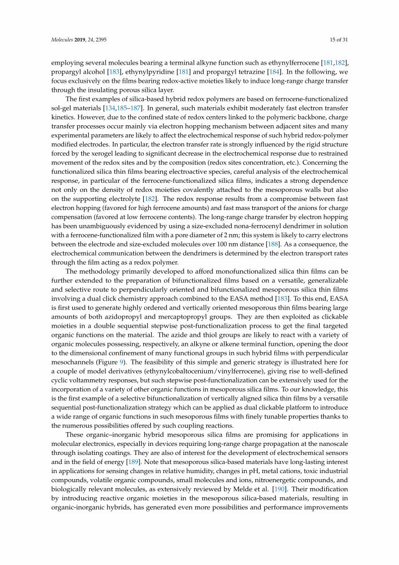
The methodology primarily developed to afford monofunctionalized silica thin films can befurther extended to the preparation of bifunctionalized films based on a versatile, generalizableand selective route to perpendicularly oriented and bifunctionalized mesoporous silica thin filmsinvolving a dual click chemistry approach combined to the EASA method [183]. To this end, EASAis first used to generate highly ordered and vertically oriented mesoporous thin films bearing largeamounts of both azidopropyl and mercaptopropyl groups. They are then exploited as clickablemoieties in a double sequential stepwise post-functionalization process to get the final targetedorganic functions on the material. The azide and thiol groups are likely to react with a variety oforganic molecules possessing, respectively, an alkyne or alkene terminal function, opening the doorto the dimensional confinement of many functional groups in such hybrid films with perpendicularmesochannels (Figure 9). The feasibility of this simple and generic strategy is illustrated here fora couple of model derivatives (ethynylcobaltocenium/vinylferrocene), giving rise to well-definedcyclic voltammetry responses, but such stepwise post-functionalization can be extensively used for theincorporation of a variety of other organic functions in mesoporous silica films. To our knowledge, thisis the first example of a selective bifunctionalization of vertically aligned silica thin films by a versatilesequential post-functionalization strategy which can be applied as dual clickable platform to introducea wide range of organic functions in such mesoporous films with finely tunable properties thanks tothe numerous possibilities offered by such coupling reactions.
These organic–inorganic hybrid mesoporous silica films are promising for applications inmolecular electronics, especially in devices requiring long-range charge propagation at the nanoscalethrough isolating coatings. They are also of interest for the development of electrochemical sensorsand in the field of energy [189]. Note that mesoporous silica-based materials have long-lasting interestin applications for sensing changes in relative humidity, changes in pH, metal cations, toxic industrialcompounds, volatile organic compounds, small molecules and ions, nitroenergetic compounds, andbiologically relevant molecules, as extensively reviewed by Melde et al. [190]. Their modificationby introducing reactive organic moieties in the mesoporous silica-based materials, resulting inorganic-inorganic hybrids, has generated even more possibilities and performance improvements

Molecules 2019, 24, 2395 16 of 31
in the design of electrochemical sensors, notably for preconcentration electroanalysis of organic andinorganic pollutants, electrocatalytic detectors and amperometric biosensors, as reported in somecomprehensive reviews [191,192].
Figure 9. An illustration of the elaboration of oriented azide-thiol-functionalized mesoporous silicafilm by EASA and subsequent derivatization of azide groups by reaction with an alkyne derivative andthe thiol ones with an alkene one.
5. Perspectives
All the applications described in the previous sections can be treated as closed chapters:supercapacitors, low-k materials and hybrids based on porous silica are thoroughly explored fromthe scientific point of view. We do not expect any breakthroughs in the near future for the first twofields, but we are confident that the numerous possibilities offered by multiple functionalizationof mesoporous silica films with organic groups would lead to significant advances in molecularelectronics by selecting the most appropriate charge transfer mediators. On the other hand, there stillexist unexplored applications for which mesoporous silica seems to be ideal. In this section, we presenttwo of them as the marker of the direction for future research.
The first concept material worthy of presentation is molecule-based realization of Hopield-likeartificial neural networks: the Molecular Neural Network (MNN).
In its original form, the Hopfield neural network was introduced in 1982 by J. J. Hopfield [193].Hopfield’s original concept of neural computation was a ground-breaking idea in the neural networksdomain, allowing for the construction of auto-associative memories [194] or systems for multi-criterionoptimization [195,196]. Contrary to existing artificial neural networks, Hopfield’s structure was noimitation of biological neural systems but a computer simulation of a spin-glass [197]. The mostimportant feature of spin-glasses, as far as Hopfield architecture is concerned, is their complex energylandscape with numerous local minima [198]. Such systems are subjects to Minimum Energy Law(as all physical systems)—only the minimum energy configuration is stable. Such systems show aslow drift towards their minimum of the energy function (Hamiltonian). In the spin-glass, the energylandscape is fully determined by the value of exchange interactions between contributed atomicspins. The evolution of the system depends on continuous adjustment of the atom spins orientationin response to magnetic fields originating either from other atoms or external ones. As any otherphysical system, spin-glass also continuously approaches its minimum energy configuration during itsevolution. Such a configuration is stable and does not change in time. Thus, spin-glass has a property

Molecules 2019, 24, 2395 17 of 31
of a total energy minimization (Hamilton function)—the only possible stable state of thpie atomic spinscorresponds to the local energy minimum. Interestingly, this property can be used to build neuralcomputational systems. Hopfield’s idea was simple: the description of a problem can be given by thecouplings (or so-called interconnection strengths) in the sense that the energy minimum correspondsto the solution (where the interconnections create the energy landscape), i.e. the solution in the form ofthe minimum-energy configuration of a spin-glass is found as a result of its relaxation. His computerrealization of the spin-glass involved substitution of atoms by neurons, exchanging interactions byinterconnections strengths and creating neural networks, as shown in Figure 10.
v1
å gu1
åu2 v2
åuN vN
t2N
tN1
t1N
g
g
t12
tN2
t22
tNN
t21
t11
Figure 10. The structure of the Hopfield-like continuous neural network. In the picture, tik is aninterconnection strength between the neuron i and k, ui is internal potential of neuron i, and g is acontinuous activation function (usually sigmoidal) with given external potentials vi = g(ui).
To solve the optimization problem by a Hopfield Neural network, the problem A must be writtenin a proper form. Conditions that must be fulfilled can be written as follows:
1. The problem ,must be formulated in such a way that each syntactically correct solutioncorresponds to the local energy minima.
2. A lower energy minimum corresponds to s better solution.3. The best solution corresponds to the global minimum.
It should be expressed in the square form allowing for calculation of the interconnection strengthsby comparison of the problem formulation to the Hamilton function, similar to for the spin-glass.The transformation of optimization problem A into s form that would be accepted by Hopfield neuralnetwork depends on selecting of interconnection strengths tij in such a way that the solution of theproblem represents energy minima fulfilling Conditions 1–3. Then, the problem can be solved by theneural network during its relaxation: the network “points out” the position of the energy minimum bythe configuration of the external states vi. A detailed description of the minimization procedure byusing Hopfield neural network can be found elsewhere [199].
The idea was revolutionary. However, thus far some practical implementations of this idea havenot met the expectations. In many fields (e.g., associative memories), Hopfield networks have beenapplied providing the best solution. Nevertheless, due to the constraints of these systems, they couldonly mimic the original Hopfield’s concept. In the real working conditions, the computer simulationsof the Hopfield neural networks stacked in local minima, shows errors connected with discretization

Molecules 2019, 24, 2395 18 of 31
and worked in a such a slow manner that using of the neural algorithm in a real-time working deviceswas impossible. All these problems originate from one important feature: Hopfield-like networks onlyimitates spin-glass.
The solution could be a “step back” to original spin-glasses as they can operate in a parallel way.Unfortunately, its implementation is challenging since both the determination of couplings betweenneurons and checking the spin states of neurons are hardly possible. Nevertheless, all these problemscan be solved by the enlargement of the spin-glass to the dimension giving possibility of reading theconfiguration of atoms/nodes/neurons (next called processing units) and setting interconnectionsstrengths between processing units (energy landscape shaping).
In this way, we can precisely define the necessity: the layout of small bistable units connectedin such a way that they can interact with each other (parallel continuous operating). At the sametime, processing units should be large enough to allow reading their configuration and controllinginterconnections. Processing units should be distributed in a 2D regular way. The regularity ofdistribution facilitates localization, connections and states reading. Such a layout could operate muchfaster and more precisely as a computer simulation of a Hopfield network. Such a proposed devicecan work as spin-glass and not only imitate it.
Proposed device can be based on vertically-aligned mesoporous silica thin film. There, porouslayer is a template allowing for the regular distribution of the magnetic molecules in the roles ofprocessing units. Moreover, silica walls shield magnetic interactions between neighboring processingunits. We propose using the electro-assisted self-assembly method for fabrication of the silicatemplate [40] to obtain thin silica layers containing highly 2D ordered vertically aligned channels, asdescribed in previous section (see Figure 8). Each pore filled by some magnetic molecule behaves as abistable (or sigmoidal) processing units. Taking under consideration the geometry of such thin film, itis possible to obtain huge neurons density: 13 × ∼1010 units in mm2. Now, one of the most importantquestion is: How can processing units inside silica pores be achieved? This can be done by a veryprecise functionalization of the pores bottom by single-molecule magnets with assumed magnetic andstructural properties. We aim for molecules with relatively high ground spin and dimensions littlelower than the diameter of the pores. High magnetic moment allows for reading of the magnetic statesof molecules (MFM or XMCD). Dimensions close to the diameter of the pores assure that each porewill contain only one magnetic molecule anchored at the bottom. The ideal candidate seems to beMn12-stearate single molecule magnet [200]—a soluble derivative of Mn12-ac16 [201]. The manganesecore shows a high intrinsic spin (S = 10) and a slow relaxation of magnetization [202].
Other important questions arise: How can such a precise functionalization be performed? Howcan a single Mn12-stearate molecule in each pore be obtained? The method which makes this possible isa multi-step functionalization (MSF) procedure that has been already tested with good results [203]: wehave shown that it is possible to anchor the metal ions exclusively at the pores bottom. The procedurecan be applied also for functionalization by Mn12-stearate molecule. Taking under considerationdimensions of these SMMs (a shape that can be inscribed into a flattened ellipsoid with dimensions of1.5, 2.5 and 3 nm depending on the observation angle), the application of MSF assures the anchoring ofsingle SMM inside each pore, as shown in Figure 11.

Molecules 2019, 24, 2395 19 of 31
FTO-glass withpropyl-CN groups
anchoring units(propyl-COOH)
vertically alignedmesoporous silicathin film.
functionalization byMn -stearate12
single-molecule magnets
substrate
precursors of anchoringunits (propyl-CN)
the deposition ofvertically-alignedporous silica layer
activation of CN unitsto COOH anchoringgroups
Mn -stearate12
regular layoutof Mn -stearate12
single-molecule magnetsshielded by silica walls
Figure 11. A schematic representation of the synthesis procedure for fabrication of vertically alignedthin mesoporous silica layers containing singular Mn12-stearate molecules at the bottom of channels.
It may be doubtful whether or not it is possible to separate and attach the Mn12-stearate SMMsbut this possibility was also tested and directly observed under TEM (Mn12-st were separated ontospherical silica surface (see Figure 12) [204].
5 nm
Figure 12. The transmission electron micrographs of the individual Mn12-stearate molecules attachedto the spherical silica surface.
Looking at the preliminary results and the initial research presented above, we are convinced thatpreparation of the regular layout of the independent magnetic units is feasible. Surely, such a devicewill be operating only at a low temperatures below the blocking point (3 K). Now, we face one importantproblem: how to connect the processing units and how to control the interconnection strengths. Here,we can only propose a solution. In our opinion, the control of processing units interactions betweeneach other can be realized through Fermi electrons as in the case of spin-glass [198]. Exchange strengthscan be tuned by adjusting the coherence of electrons. Obviously, the coherent way of electron is muchshorter than the distance between processing units. However. this problem can potentially be solvedby conversion into a spin-wave [205] and using a Datta–Das [206] transistor for coherence adjusting,as shown in Figure 13.

Molecules 2019, 24, 2395 20 of 31
verticallyalignedporous silica
Mn -st12
molecule
electrode
interconnection strenghtcontroller: tunner ofelectron coherence
converting unit-equivalent of atomin Ising model
connectorspin-wave path
magnetic interactions betweenmolecules in different pores areshielded by silica walls
e e ee e e
e e
e e
e
e
ee
e
e
e
e
e
e
substrate
Figure 13. A schematic illustration of the molecular neural network with two interacting molecularneurons (processing units).
Here, we must remark that the connection of processing units can be an extremely difficulttask—there are numerous problems to overcome. Nevertheless, in our opinion, scientific researchshould give the possibility to go beyond assumed frameworks or, actually, even broaden all theframeworks and limitations. The concept of molecular neural networks seems to be worth of extensivescientific efforts.
A somewhat anologous and simplified concept can be used for the construction of super-densemagnetic memory storage device. Nevertheless, we must mention that simplified does not mean easyto fabricate. The concept device can be defined as a regular layout of separate, independent permanentmagnetic units with the diameter of approximately 2 nm. Additionally, the units should be separatedfrom each other by silica walls with the thickness of 1 nm. The magnetic units are placed insidevertically aligned (perpendicularly to the substrate) silica pores arranged 2D hexagonally, as shownin Figure 14.
2D ordered porous silica layerwith permanent magnets in pores
substrate
silica pores with permanentmagnetic specimen inside
substrate
silica walls
2D orderedporoussilica layer
(a) (b)
Figure 14. The structure of the silica-based memory storage device: perspective projection (a); andcross section (b).
The thickness of such a layer is in the range of 70–100 nm. We assume that magnetic states ofthe units can be kept at room temperature. Similarly, this task also seems to be extremely difficult.How can permanent magnets operating in room temperature inside the pores of diameter of 2 nmbe fabricated? According to our preliminary research, it is possible. The silica pores play the roleof dishes that can be filled by a permanent magnetic specimen: magnetite (Fe3O4). Mesochannelscan be considered as nano-reactors enabling super-precise control of the concentration of reagents.This can be done by precise functionalization of the pores interiors by ferrous ions [207]. Assuming thecorrect concentration of the internal propyl iron phosphonate units, it is possible to create magnetitenanocrystals inside nanoreactors as a result of a thermal decomposition by precisely controllingselected heating parameters (temperature, heating rate and atmosphere), as shown in Figure 15a.

Molecules 2019, 24, 2395 21 of 31
substrate
mesoporoussilicalayer
ferrous ionanchoring unit
substrate
mesoporoussilicalayer
Magnetite
thermaldecomposition
silicawall
PO
Fe
-2+
O-
O
propyl chain
10 nm
(a) (b)
Figure 15. The general illustration the procedure of magnetite synthesis by the use of silica nanoreactors(a); and resulting nanoparticles of magnetite obtained inside SBA-15 (TEM image) (b).
We tested the procedure with the use of SBA-15 silica as a matrix—powdered form of silica allowedfor convenient performing of research. We obtained fine nano-crystals inside silica pores with diameterof below 4.7 nm (see Figure 15b). The crystals were identified as a magnetite. Moreover, they showedmagnetic hysteresis at the room temperature despite their low diameters (below super-paramagneticlimit). We admit we are not entirely sure of the reasons for this phenomenon. Currently, we can onlytheorize that it is a result of the spatial confinements (article under preparation). Nevertheless, all theresults shoved us that the fabrication of the porous silica-based super dense memory storage systemis possible.
Both concepts presented above are challenging for realization. However, looking at thepreliminary results we, are convinced about their feasibility. Moreover, their applicative potentialseems to justify all scientific efforts toward fabrication of the presented devices.
6. Conclusions
Over the years, electronics have become a larger and larger part of our lives to the point where westop noticing them. The behind-the-scenes work of researchers to keep improving them described hereshines a light on the complex mechanisms involved in this process. Understanding these phenomenaallows for searching for novel materials applicable in electronics.
On the brink of the end of the silicon era, mesoporous silica is potentially the next standard asthe base material used in electronics. Tailorable properties through different routes of the bottom-upsyntheses, flexible functionalization and the new emerging fields of science in which the material canbe applied make mesoporous silica-based materials an exciting alternative.
Here, we describe this material in such a context. We present d the development and most crucialfindings of mesoporous silica as far as electronic devices are concerned. Porous silica are commonlyused in several domains, including an industrial use. Obviously, there also exist less explored domainswhere these porous materials have just been introduced.
Concerning the former case, supercapacitors, low-k materials or sensors are good examples. Here,porous silica is an evident material for the fabrication of electrodes or interlevel dielectrics. This fieldis well described by numerous publications including some reviews.
The latter case concerns emerging technologies. Here, the literature coverage is lacking.We present a few examples of such possible applications: the molecular neural network and silica-basesuper-dense magnetic memory storage. It can be treated as a preliminary communication on conceptdevices or as inspiration for further scientific works.

Molecules 2019, 24, 2395 22 of 31
The demand will drive the supply and new exciting discoveries in the field of electronics are sureto come. Indeed, scientists even search for more and more sophisticated devices to conduct research.
Funding: This research was funded by National Centre of Science (Grant No. 2017/26/E/ST5/00162).
Acknowledgments: The authors are grateful to Maciej Zubko for performing TEM microscopy.
Conflicts of Interest: The authors declare no conflict of interest.
Abbreviations
The following abbreviations are used in this manuscript:
TEOS tetraethoxy silaneTMOS tetramethoxy silaneTMES trimethylethoxysilaneMTMS methyltrimethoxy silaneOTMS octyltrimethoxy silaneAPTMS 3-aminopropyl trimethoxy silaneMe methyl unitsEt ethyl unitsCTAB C16H33 − N(CH3)
+3 Br−
CTACl C16H33 − N(CH3)+3 Cl−
Brij76 C18H37(OCH2CH2)10OHBrij56 C16H33(OCH2CH2)10OHBrij30 C12H25(OCH2CH2)4OHPluronic F127 poly(ethylene oxide)-poly(propylene oxide)-poly(ethylene oxide) triblock copolymer:
PEO106-PPO70-PEO106Pluronic P123 poly(ethylene oxide)-poly(propylene oxide)-poly(ethylene oxide) triblock copolymer:
PEO20-PPO70-PEO20
ALD atomic layer depositionOTES-POS octa(triethoxysilylethyl)polyhedral oligomeric silsesquioxaneMFM magnetic force microscopyXMCD X-ray magnetic circular dichroismSMM single-molecule magnetMn12-ac16 [Mn12O12(CH3(CH2)16CO2)11(CH3CO2)5(H2O)4] · 2CH3COOHMn12-st derivative of Mn12 containing strearic acid ligandsMSF multi-step functionalization procedure
References
1. Horowitz, P.; Hill, W. The Art of Electronics; Cambridge University Press: Cambridge, MA, USA, 1989.2. Tietze, U.; Schenk, C.; Schmid, E. Advanced Electronic Circuits; Springer: New York, NY, USA, 1991.3. Tietze, U.; Schenk, C.; Gamm, E. Electronic Circuits: Handbook for Design and Application; Springer: New York,
NY, USA, 2015.4. De Forest, L. The audion: A new receiver for wireless telegraphy. Proc. Am. Inst. Electr. Eng. 1906, 25,
719–747. [CrossRef]5. Boot, H.; Randall, J. The cavity magnetron. J. Inst. Electr. Eng. Part IIIA Radiolocat. 1946, 93, 928–938.
[CrossRef]6. Blanchard, Y.; Galati, G.; Van Genderen, P. The cavity magnetron: Not just a british invention [Historical
Corner]. IEEE Antennas Propag. Mag. 2013, 55, 244–254. [CrossRef]7. Wolff, C. Radar Tutorial (Book 1): Radar Basics. Radartutorial Webpage. Available online: www.radartutorial.
eu (accessed on 28 June 2019).8. Copeland, J.; Haeff, A.A. The true history of the traveling wave tube. IEEE Spectr. 2015, 52, 38–43. [CrossRef]9. Gilmour, A. Klystrons, Traveling Wave Tubes, Magnetrons, Crossed-Field Amplifiers, and Gyrotrons; Artech House:
London, UK, 2011.10. Gilmour, A. Principles of Traveling Wave Tubes; Artech House: London, UK, 1994.

Molecules 2019, 24, 2395 23 of 31
11. Vardalas, J. Twists and Turns in the Development of the Transistor. In IEEE-USA Today’s Engineer; IEEE:Piscataway, NJ, USA, 2003.
12. Riordan, M.; Hoddeson, L.; Herring, C. The invention of the transistor. In More Things in Heaven and Earth;Springer: New York, NY, USA, 1999; pp. 563–578.
13. Brinkman, W.F.; Haggan, D.E.; Troutman, W.W. A history of the invention of the transistor and where it willlead us. IEEE J. Solid-State Circuits 1997, 32, 1858–1865. [CrossRef]
14. Gray, P.R.; Hurst, P.; Meyer, R.G.; Lewis, S. Analysis and Design of Analog Integrated Circuits; Wiley: New York,NY, USA, 2001.
15. Schaller, R.R. Moore’s law: Past, present and future. IEEE Spectr. 1997, 34, 52–59. [CrossRef]16. Meindl, J.D. Beyond Moore’s law: The interconnect era. Comput. Sci. Eng. 2003, 5, 20–24. [CrossRef]17. Zalasinski, M.; Cpałka, K. Novel algorithm for the on-line signature verification. In International Conference
on Artificial Intelligence and Soft Computing; Springer: Berlin, Germany, 2012; pp. 362–367.18. Cpalka, K.; Łapa, K.; Przybył, A. Genetic Programming Algorithm for Designing of Control Systems.
Inf. Technol. Control 2018, 47, 668–683. [CrossRef]19. Wu, X.; Lee, I.; Dong, Q.; Yang, K.; Kim, D.; Wang, J.; Peng, Y.; Zhang, Y.; Saliganc, M.; Yasuda, M.; et
al. A 0.04 MM 3 16NW Wireless and Batteryless Sensor System with Integrated Cortex-M0+ Processorand Optical Communication for Cellular Temperature Measurement. In Proceedings of the 2018 IEEESymposium on VLSI Circuits, Honolulu, HI, USA, 18–22 June 2018; pp. 191–192.
20. Salahuddin, S.; Ni, K.; Datta, S. The era of hyper-scaling in electronics. Nat. Electron. 2018, 1, 442. [CrossRef]21. Deleonibus, S. Electronic Devices Architectures for the NANO-CMOS Era; Pan Stanford Publishing:
Singapore, 2009.22. Waldrop, M.M. The chips are down for Moore’s law. Nat. News 2016, 530, 144. [CrossRef]23. Beck, J.S.; Vartuli, J.; Roth, W.J.; Leonowicz, M.; Kresge, C.; Schmitt, K.; Chu, C.; Olson, D.H.; Sheppard, E.;
McCullen, S.; et al. A new family of mesoporous molecular sieves prepared with liquid crystal templates.J. Am. Chem. Soc. 1992, 114, 10834–10843. [CrossRef]
24. Chen, C.Y.; Li, H.X.; Davis, M.E. Studies on mesoporous materials: I. Synthesis and characterization ofMCM-41. Microporous Mater. 1993, 2, 17–26. [CrossRef]
25. Jehng, J.M.; Tung, W.C.; Kuo, C.H. The formation mechanisms of multi-wall carbon nanotubes over the Nimodified MCM-41 catalysts. J. Porous Mater. 2008, 15, 43–51. [CrossRef]
26. Zhao, D.; Feng, J.; Huo, Q.; Melosh, N.; Fredrickson, G.H.; Chmelka, B.F.; Stucky, G.D. Triblock copolymersyntheses of mesoporous silica with periodic 50 to 300 angstrom pores. Science 1998, 279, 548–552. [CrossRef][PubMed]
27. Zhao, D.; Huo, Q.; Feng, J.; Chmelka, B.F.; Stucky, G.D. Nonionic triblock and star diblock copolymer andoligomeric surfactant syntheses of highly ordered, hydrothermally stable, mesoporous silica structures.J. Am. Chem. Soc. 1998, 120, 6024–6036. [CrossRef]
28. Xu, R.; Pang, W.; Yu, J.; Huo, Q.; Chen, J. Chemistry of Zeolites and Related Porous Materials: Synthesis andStructure; John Wiley & Sons: Singapore, 2009.
29. Imperor-Clerc, M.; Davidson, P.; Davidson, A. Existence of a microporous corona around the mesopores ofsilica-based SBA-15 materials templated by triblock copolymers. J. Am. Chem. Soc. 2000, 122, 11925–11933.[CrossRef]
30. Ryoo, R.; Ko, C.H.; Kruk, M.; Antochshuk, V.; Jaroniec, M. Block-copolymer-templated ordered mesoporoussilica: Array of uniform mesopores or mesopore- micropore network? J. Phys. Chem. B 2000, 104, 11465–11471.[CrossRef]
31. Dos Santos, S.M.L.; Nogueira, K.A.B.; de Souza Gama, M.; Lima, J.D.F.; da Silva Júnior, I.J.; de Azevedo, D.C.S.Synthesis and characterization of ordered mesoporous silica (SBA-15 and SBA-16) for adsorption ofbiomolecules. Microporous Mesoporous Mater. 2013, 180, 284–292. [CrossRef]
32. Thielemann, J.P.; Girgsdies, F.; Schlögl, R.; Hess, C. Pore structure and surface area of silica SBA-15: Influenceof washing and scale-up. Beilstein J. Nanotechnol. 2011, 2, 110–118. [CrossRef]
33. Kruk, M.; Jaroniec, M.; Ko, C.H.; Ryoo, R. Characterization of the porous structure of SBA-15. Chem. Mater.2000, 12, 1961–1968. [CrossRef]
34. Guari, Y.; Thieuleux, C.; Mehdi, A.; Reyé, C.; Corriu, R.J.; Gomez-Gallardo, S.; Philippot, K.; Chaudret, B.In situ formation of gold nanoparticles within thiol functionalized HMS-C16 and SBA-15 type materials viaan organometallic two-step approach. Chem. Mater. 2003, 15, 2017–2024. [CrossRef]

Molecules 2019, 24, 2395 24 of 31
35. Maria Chong, A.; Zhao, X. Functionalization of SBA-15 with APTES and characterization of functionalizedmaterials. J. Phys. Chem. B 2003, 107, 12650–12657. [CrossRef]
36. Boury, B.; Corriu, R. Auto-Organization in Sol-Gel Type Polycondensation: A Door to the Nanosciences.Chem. Rec. 2003, 3, 120–132. [CrossRef] [PubMed]
37. Yeh, Y.Q.; Lin, H.P.; Tang, C.Y.; Mou, C.Y. Mesoporous silica SBA-15 sheet with perpendicular nanochannels.J. Colloid Interface Sci. 2011, 362, 354–366. [CrossRef] [PubMed]
38. Johansson, E.M.; Córdoba, J.M.; Odén, M. Synthesis and characterization of large mesoporous silica SBA-15sheets with ordered accessible 18 nm pores. Mater. Lett. 2009, 63, 2129–2131. [CrossRef]
39. Hao, N.; Tang, F.; Li, L. MCM-41 mesoporous silica sheet with ordered perpendicular nanochannels forprotein delivery and the assembly of Ag nanoparticles in catalytic applications. Microporous MesoporousMater. 2015, 218, 223–227. [CrossRef]
40. Walcarius, A.; Sibottier, E.; Etienne, M.; Ghanbaja, J. Electrochemically assisted self-assembly of mesoporoussilica thin films. Nat. Mater. 2007, 6, 602. [CrossRef] [PubMed]
41. Bardeau, J.F.; Gourbil, A.; Dutreilh-Colas, M.; Dourdain, S.; Mehdi, A.; Gibaud, A. X-ray reflectivity studyof acid–base post-synthesis treatments of mesoporous thin films templated by P123. Thin Solid Film. 2006,495, 191–196. [CrossRef]
42. Teng, Z.; Zheng, G.; Dou, Y.; Li, W.; Mou, C.Y.; Zhang, X.; Asiri, A.M.; Zhao, D. Highly ordered mesoporoussilica films with perpendicular mesochannels by a simple stöber-solution growth approach. Angew. Chem.Int. Ed. 2012, 51, 2173–2177. [CrossRef]
43. Lu, M. Supercapacitors: Materials, Systems, and Applications; John Wiley & Sons: Singapore, 2013.44. Yu, A.; Chabot, V.; Zhang, J. Electrochemical Supercapacitors for Energy Storage and Delivery: Fundamentals and
Applications; CRC Press: New York, NY, USA, 2013.45. Conway, B.E. Electrochemical Supercapacitors: Scientific Fundamentals and Technological Applications; Springer
Science & Business Media: New York, NY, USA, 2013.46. Moussa, M.; El-Kady, M.F.; Zhao, Z.; Majewski, P.; Ma, J. Recent progress and performance evaluation
for polyaniline/graphene nanocomposites as supercapacitor electrodes. Nanotechnology 2016, 27, 442001.[CrossRef]
47. Jiang, Y.; Liu, J. Definitions of Pseudocapacitive Materials: A Brief Review. Energy Environ. Mater. 2019, 2,30–37. [CrossRef]
48. Lu, W.; Dai, L. Carbon nanotube supercapacitors. In Carbon Nanotubes; IntechOpen: London, UK, 2010.49. Ma, W.; Chen, S.; Yang, S.; Chen, W.; Weng, W.; Zhu, M. Bottom-up fabrication of activated carbon fiber for
all-solid-state supercapacitor with excellent electrochemical performance. ACS Appl. Mater. Interfaces 2016,8, 14622–14627. [CrossRef] [PubMed]
50. Divyashree, A.; Hegde, G. Activated carbon nanospheres derived from bio-waste materials for supercapacitorapplications—A review. RSC Adv. 2015, 5, 88339–88352.
51. Du, C.; Pan, N. High power density supercapacitor electrodes of carbon nanotube films by electrophoreticdeposition. Nanotechnology 2006, 17, 5314. [CrossRef]
52. Du, C.; Yeh, J.; Pan, N. High power density supercapacitors using locally aligned carbon nanotube electrodes.Nanotechnology 2005, 16, 350. [CrossRef]
53. Du, C.; Pan, N. Carbon nanotube-based supercapacitors. Nanotechnol. Law Bus. 2007, 4, 3.54. Lee, H.M.; Lee, K.; Kim, C.K. Electrodeposition of manganese-nickel oxide films on a graphite sheet for
electrochemical capacitor applications. Materials 2014, 7, 265–274. [CrossRef] [PubMed]55. Liew, C.W.; Ramesh, S. Comparing triflate and hexafluorophosphate anions of ionic liquids in polymer
electrolytes for supercapacitor applications. Materials 2014, 7, 4019–4033. [CrossRef]56. Yun, Y.S.; Im, C.; Park, H.H.; Hwang, I.; Tak, Y.; Jin, H.J. Hierarchically porous carbon nanofibers containing
numerous heteroatoms for supercapacitors. J. Power Sources 2013, 234, 285–291. [CrossRef]57. Yang, X.; Li, Z.; Zhi, J.; Ma, J.; Hu, A. Synthesis of Ultrathin Mesoporous Carbon through Bergman
Cyclization of Enediyne Self-Assembled Monolayers in SBA-15. Langmuir 2010, 26, 11244–11248. [CrossRef]58. Zhi, J.; Song, D.; Li, Z.; Lei, X.; Hu, A. Palladium nanoparticles in carbon thin film-lined SBA-15
nanoreactors: Efficient heterogeneous catalysts for Suzuki–Miyaura cross coupling reaction in aqueousmedia. Chem. Commun. 2011, 47, 10707–10709. [CrossRef] [PubMed]

Molecules 2019, 24, 2395 25 of 31
59. Zhi, J.; Wang, Y.; Deng, S.; Hu, A. Study on the relation between pore size and supercapacitance inmesoporous carbon electrodes with silica-supported carbon nanomembranes. RSC Adv. 2014, 4, 40296–40300.[CrossRef]
60. Zhi, J.; Deng, S.; Wang, Y.; Hu, A. Highly Ordered Metal Oxide Nanorods inside Mesoporous SilicaSupported Carbon Nanomembranes: High Performance Electrode Materials for Symmetrical SupercapacitorDevices. J. Phys. Chem. C 2015, 119, 8530–8536, [CrossRef]
61. Wang, W.; Shan, W.; Ru, H.; Wu, N. A facile and versatile partitioned cooperative self-assembly process toprepare SBA-15s with larger mesopores, high microporosity and tunable particle sizes. J. Mater. Chem. 2011,21, 12059–12067. [CrossRef]
62. Fulvio, P.F.; Pikus, S.; Jaroniec, M. Tailoring properties of SBA-15 materials by controlling conditions ofhydrothermal synthesis. J. Mater. Chem. 2005, 15, 5049–5053. [CrossRef]
63. Numao, S.; Judai, K.; Nishijo, J.; Mizuuchi, K.; Nishi, N. Synthesis and characterization of mesoporouscarbon nano-dendrites with graphitic ultra-thin walls and their application to supercapacitor electrodes.Carbon 2009, 47, 306–312. [CrossRef]
64. Huang, Y.; Li, Y.; Hu, Z.; Wei, G.; Guo, J.; Liu, J. A carbon modified MnO2 nanosheet array as a stablehigh-capacitance supercapacitor electrode. J. Mater. Chem. A 2013, 1, 9809–9813. [CrossRef]
65. Mu, J.; Chen, B.; Guo, Z.; Zhang, M.; Zhang, Z.; Shao, C.; Liu, Y. Tin oxide (SnO2) nanoparticles/electrospuncarbon nanofibers (CNFs) heterostructures: Controlled fabrication and high capacitive behavior. J. ColloidInterface Sci. 2011, 356, 706–712. [CrossRef] [PubMed]
66. Singh, A.K.; Sarkar, D.; Khan, G.G.; Mandal, K. Unique hydrogenated Ni/NiO core/shell 1Dnano-heterostructures with superior electrochemical performance as supercapacitors. J. Mater. Chem. A 2013,1, 12759–12767. [CrossRef]
67. Hu, Z.; Zu, L.; Jiang, Y.; Lian, H.; Liu, Y.; Wang, X.; Cui, X. High performance nanocomposite electrodes ofmesoporous silica platelet-polyaniline synthesized via impregnation polymerization. Polym. Compos. 2017,38, 1616–1623. [CrossRef]
68. Silva, R.; Asefa, T. Noble metal-free oxidative electrocatalysts: Polyaniline and Co(II)-polyanilinenanostructures hosted in nanoporous silica. Adv. Mater. 2012, 24, 1878–1883. [CrossRef] [PubMed]
69. Javed, M.; Abbas, S.M.; Siddiq, M.; Han, D.; Niu, L. Mesoporous silica wrapped with grapheneoxide-conducting PANI nanowires as a novel hybrid electrode for supercapacitor. J. Phys. Chem. Solids 2018,113, 220–228. [CrossRef]
70. Wang, Y.G.; Xia, Y.Y. Electrochemical capacitance characterization of NiO with ordered mesoporous structuresynthesized by template SBA-15. Electrochim. Acta 2006, 51, 3223–3227. [CrossRef]
71. Ghimbeu, C.M.; Malak-Polaczyk, A.; Frackowiak, E.; Vix-Guterl, C. Template-derived high surface areaλ-MnO 2 for supercapacitor applications. J. Appl. Electrochem. 2014, 44, 123–132. [CrossRef]
72. Jun, S.; Joo, S.H.; Ryoo, R.; Kruk, M.; Jaroniec, M.; Liu, Z.; Ohsuna, T.; Terasaki, O. Synthesis of New,Nanoporous Carbon with Hexagonally Ordered Mesostructure. J. Am. Chem. Soc. 2000, 122, 10712–10713,[CrossRef]
73. Wang, D.W.; Feng, L.I.; Min LI, U.; Cheng, H.M. Improved capacitance of SBA-15 templated mesoporouscarbons after modification with nitric acid oxidation. New Carbon Mater. 2007, 22, 307–314. [CrossRef]
74. Singh, D.K.; Krishna, K.S.; Harish, S.; Sampath, S.; Eswaramoorthy, M. No More HF: Teflon-Assisted UltrafastRemoval of Silica to Generate High-Surface-Area Mesostructured Carbon for Enhanced CO2 Capture andSupercapacitor Performance. Angew. Chem. Int. Ed. 2016, 55, 2032–2036. [CrossRef]
75. Zhi, J.; Deng, S.; Zhang, Y.; Wang, Y.; Hu, A. Embedding CO3O4 nanoparticles in SBA-15 supported carbonnanomembrane for advanced supercapacitor materials. J. Mater. Chem. A 2013, 1, 3171–3176. [CrossRef]
76. Huang, H.S.; Chang, K.H.; Suzuki, N.; Yamauchi, Y.; Hu, C.C.; Wu, K.C.W. Evaporation-InducedCoating of Hydrous Ruthenium Oxide on Mesoporous Silica Nanoparticles to Develop High-PerformanceSupercapacitors. Small 2013, 9, 2520–2526. [CrossRef]
77. Chiang, Y.D.; Lian, H.Y.; Leo, S.Y.; Wang, S.G.; Yamauchi, Y.; Wu, K.C.W. Controlling particle size andstructural properties of mesoporous silica nanoparticles using the Taguchi method. J. Phys. Chem. C 2011,115, 13158–13165. [CrossRef]
78. Jonscher, A.K. Dielectric relaxation in solids. J. Phys. D Appl. Phys. 1999, 32, R57. [CrossRef]79. Kremer, F.; Schönhals, A. Broadband Dielectric Spectroscopy; Springer Science & Business Media: New York,
NY, USA, 2012.

Molecules 2019, 24, 2395 26 of 31
80. Maier, G. Low dielectric constant polymers for microelectronics. Prog. Polym. Sci. 2001, 26, 3–65. [CrossRef]81. Ho, P.S.; Leu, J. Low Dielectric Constant Materials for IC Applications; Springer Science & Business Media:
New York, NY, USA, 2003; Volume 9.82. Croes, K.; Pantouvaki, M.; Carbonell, L.; Zhao, L.; Beyer, G.; Tokei, Z. Comparison between intrinsic and
integrated reliability properties of low-k materials. In Proceedings of the 2011 International ReliabilityPhysics Symposium, Monterey, CA, USA, 10–14 April 2011; pp. 2–3.
83. Gupta, T. Copper Interconnect Technology; Springer Science & Business Media: New York, NY, USA, 2010.84. Böttcher, C.J.F.; van Belle, O.C.; Bordewijk, P.; Rip, A. Theory of Electric Polarization; Elsevier Science Ltd.:
Munich, Germany, 1978; Volume 2.85. Ferradini, C.; Jay-Gerin, J.P. Excess Electrons in Dielectric Media; CRC Press: New York, NY USA, 1991.86. Shamiryan, D.; Abell, T.; Iacopi, F.; Maex, K. Low-k dielectric materials. Mater. Today 2004, 7, 34–39.
[CrossRef]87. Prakash, S.S.; Brinker, C.J.; Hurd, A.J.; Rao, S.M. Silica aerogel films prepared at ambient pressure by using
surface derivatization to induce reversible drying shrinkage. Nature 1995, 374, 439. [CrossRef]88. Prakash, S.S.; Brinker, C.J.; Hurd, A.J. Silica aerogel films at ambient pressure. J. Non-Cryst. Solids 1995,
190, 264–275. [CrossRef]89. Jin, C.; Luttmer, J.; Smith, D.M.; Ramos, T.A. Nanoporous silica as an ultralow-k dielectric. MRS Bull. 1997,
22, 39–42. [CrossRef]90. Lu, Y.; Ganguli, R.; Drewien, C.A.; Anderson, M.T.; Brinker, C.J.; Gong, W.; Guo, Y.; Soyez, H.; Dunn, B.;
Huang, M.H.; et al. Continuous formation of supported cubic and hexagonal mesoporous films by sol–geldip-coating. Nature 1997, 389, 364. [CrossRef]
91. Baskaran, S.; Liu, J.; Domansky, K.; Kohler, N.; Li, X.; Coyle, C.; Fryxell, G.E.; Thevuthasan, S.; Williford, R.E.Low dielectric constant mesoporous silica films through molecularly templated synthesis. Adv. Mater. 2000,12, 291–294. [CrossRef]
92. Bruinsma, P.J.; Kim, A.Y.; Liu, J.; Baskaran, S. Mesoporous silica synthesized by solvent evaporation: Spunfibers and spray-dried hollow spheres. Chem. Mater. 1997, 9, 2507–2512. [CrossRef]
93. Zhao, D.; Yang, P.; Melosh, N.; Feng, J.; Chmelka, B.F.; Stucky, G.D. Continuous mesoporous silica films withhighly ordered large pore structures. Adv. Mater. 1998, 10, 1380–1385. [CrossRef]
94. Wirnsberger, G.; Yang, P.; Scott, B.J.; Chmelka, B.F.; Stucky, G.D. Mesostructured materials for opticalapplications: From low-k dielectrics to sensors and lasers. Spectrochim. Acta Part A Mol. Biomol. Spectrosc.2001, 57, 2049–2060. [CrossRef]
95. Cho, A.; Pan, F.; Chao, K.; Liu, P.; Chen, J. The preparation of mesoporous silica ultra-low-k film using ozoneashing treatment. Thin Solid Film. 2005, 483, 283–286. [CrossRef]
96. Tanaka, S.; Tada, H.; Maruo, T.; Nishiyama, N.; Egashira, Y.; Ueyama, K. Vapor infiltration techniques forspin-on mesoporous silica films. Thin Solid Film. 2006, 495, 186–190. [CrossRef]
97. Maruo, T.; Tanaka, S.; Hillhouse, H.W.; Nishiyama, N.; Egashira, Y.; Ueyama, K. Disordered mesoporoussilica low-k thin films prepared by vapor deposition into a triblock copolymer template film. Thin Solid Film.2008, 516, 4771–4776. [CrossRef]
98. Min, C.K.; Wu, T.B.; Yang, W.T.; Chen, C.L. Functionalized mesoporous silica/polyimide nanocompositethin films with improved mechanical properties and low dielectric constant. Compos. Sci. Technol. 2008,68, 1570–1578. [CrossRef]
99. Vengatesan, M.; Devaraju, S.; Dinakaran, K.; Alagar, M. SBA-15 filled polybenzoxazine nanocomposites forlow-k dielectric applications. J. Mater. Chem. 2012, 22, 7559–7566. [CrossRef]
100. Gunasekaran, S.; Rajakumar, K.; Alagar, M.; Dharmendirakumar, M. Design and development ofmesoporous silica reinforced skeletal modified triaryl pyridine core based polybenzoxazine (SBA-15/PBZ)nanocomposites. Int. J. Plast. Technol. 2015, 19, 309–332. [CrossRef]
101. Selvaraj, V.; Jayanthi, K.; Lakshmikandhan, T.; Alagar, M. Development of a polybenzoxazine/TSBA-15composite from the renewable resource cardanol for low-k applications. RSC Adv. 2015, 5, 48898–48907.[CrossRef]
102. Purushothaman, R. Amine functionalized SBA-15/terpolyimide composites with low dielectric constant.J. Porous Mater. 2015, 22, 585–594. [CrossRef]

Molecules 2019, 24, 2395 27 of 31
103. Devaraju, S.; Vengatesan, M.; Selvi, M.; Song, J.; Alagar, M. Mesoporous silica reinforced cyanate esternanocomposites for low k dielectric applications. Microporous Mesoporous Mater. 2013, 179, 157–164.[CrossRef]
104. de Theije, F.K.; Balkenende, A.R.; Verheijen, M.A.; Baklanov, M.R.; Mogilnikov, K.P.; Furukawa, Y. Structuralcharacterization of mesoporous organosilica films for ultralow-k dielectrics. J. Phys. Chem. B 2003, 107,4280–4289. [CrossRef]
105. Li, Z.; Li, S.; Luo, H.; Yan, Y. Effects of Crystallinity in Spin-On Pure-Silica-Zeolite MFI Low-Dielectric-ConstantFilms. Adv. Funct. Mater. 2004, 14, 1019–1024. [CrossRef]
106. Li, Z.; Lew, C.M.; Li, S.; Medina, D.I.; Yan, Y. Pure-silica-zeolite MEL low-k films from nanoparticlesuspensions. J. Phys. Chem. B 2005, 109, 8652–8658. [CrossRef] [PubMed]
107. Li, Z.; Johnson, M.C.; Sun, M.; Ryan, E.T.; Earl, D.J.; Maichen, W.; Martin, J.I.; Li, S.; Lew, C.M.; Wang, J.; et al.Mechanical and dielectric properties of pure-silica-zeolite low-k materials. Angew. Chem. Int. Ed. 2006,45, 6329–6332. [CrossRef] [PubMed]
108. Eslava, S.; Baklanov, M.R.; Neimark, A.V.; Iacopi, F.; Kirschhock, C.E.; Maex, K.; Martens, J.A. Evidence ofLarge Voids in Pure-Silica-Zeolite Low-k Dielectrics Synthesized by Spin-on of Nanoparticle Suspensions.Adv. Mater. 2008, 20, 3110–3116. [CrossRef]
109. Baklanov, M.; Green, M.; Maex, K. Dielectric Films for Advanced Microelectronics; Wiley Online Library:Singapore, 2007; Volume 12.
110. Liu, Y.; Sun, M.; Lew, C.M.; Wang, J.; Yan, Y. MEL-type Pure-Silica Zeolite Nanocrystals Prepared by anEvaporation-Assisted Two-Stage Synthesis Method as Ultra-Low-k Materials. Adv. Funct. Mater. 2008,18, 1732–1738. [CrossRef]
111. Lu, Y.; Fan, H.; Doke, N.; Loy, D.A.; Assink, R.A.; LaVan, D.A.; Brinker, C.J. Evaporation-inducedself-assembly of hybrid bridged silsesquioxane film and particulate mesophases with integral organicfunctionality. J. Am. Chem. Soc. 2000, 122, 5258–5261. [CrossRef]
112. Hatton, B.D.; Landskron, K.; Whitnall, W.; Perovic, D.D.; Ozin, G.A. Spin-Coated Periodic MesoporousOrganosilica Thin Films-Towards a New Generation of Low-Dielectric-Constant Materials. Adv. Funct. Mater.2005, 15, 823–829. [CrossRef]
113. Yang, S.; Mirau, P.A.; Pai, C.S.; Nalamasu, O.; Reichmanis, E.; Pai, J.C.; Obeng, Y.S.; Seputro, J.; Lin, E.K.;Lee, H.J.; et al. Nanoporous ultralow dielectric constant organosilicates templated by triblock copolymers.Chem. Mater. 2002, 14, 369–374. [CrossRef]
114. De Rouffignac, P.; Li, Z.; Gordon, R.G. Sealing porous low-k dielectrics with silica. Electrochem. Solid-StateLett. 2004, 7, G306–G308. [CrossRef]
115. Peters, L. Is pore sealing key to ultralow-K adoption? Semicond. Int. 2005, 28, 49–53.116. Jiang, Y.B.; Liu, N.; Gerung, H.; Cecchi, J.L.; Brinker, C.J. Nanometer-thick conformal pore sealing of
self-assembled mesoporous silica by plasma-assisted atomic layer deposition. J. Am. Chem. Soc. 2006,128, 11018–11019. [CrossRef] [PubMed]
117. Seino, M.; Wang, W.; Lofgreen, J.E.; Puzzo, D.P.; Manabe, T.; Ozin, G.A. Low-k periodic mesoporousorganosilica with air walls: POSS-PMO. J. Am. Chem. Soc. 2011, 133, 18082–18085. [CrossRef] [PubMed]
118. Zhang, L.; Abbenhuis, H.C.; Yang, Q.; Wang, Y.M.; Magusin, P.C.; Mezari, B.; van Santen, R.A.; Li, C.Mesoporous organic–inorganic hybrid materials built using polyhedral oligomeric silsesquioxane blocks.Angew. Chem. Int. Ed. 2007, 46, 5003–5006. [CrossRef] [PubMed]
119. Tsionsky, M.; Gun, G.; Glezer, V.; Lev, O. Sol-gel-derived ceramic-carbon composite electrodes: Introductionand scope of applications. Anal. Chem. 1994, 66, 1747–1753. [CrossRef]
120. Lev, O.; Wu, Z.; Bharathi, S.; Glezer, V.; Modestov, A.; Gun, J.; Rabinovich, L.; Sampath, S. Sol- gel materialsin electrochemistry. Chem. Mater. 1997, 9, 2354–2375. [CrossRef]
121. Rabinovich, L.; Lev, O. Sol-Gel Derived Composite Ceramic Carbon Electrodes. Electroanal. Int. J. DevotedFundam. Pract. Asp. Electroanal. 2001, 13, 265–275. [CrossRef]
122. Bharathi, S.; Nogami, M.; Lev, O. Electrochemical organization of gold nanoclusters in three dimensions asthin films from an aminosilicate-stabilized gold sol and their characterization. Langmuir 2001, 17, 2602–2609.[CrossRef]
123. Walcarius, A. Electroanalysis with Pure, Chemically Modified and Sol-Gel-Derived Silica-Based Materials.Electroanal. Int. J. Devoted Fundam. Pract. Asp. Electroanal. 2001, 13, 701–718. [CrossRef]

Molecules 2019, 24, 2395 28 of 31
124. Mousty, C.; Walcarius, A. Electrochemically assisted deposition by local pH tuning: A versatile tool togenerate ordered mesoporous silica thin films and layered double hydroxide materials. J. Solid StateElectrochem. 2015, 19, 1905–1931. [CrossRef]
125. Gangopadhyay, R.; De, A. Conducting polymer nanocomposites: A brief overview. Chem. Mater. 2000,12, 608–622. [CrossRef]
126. Walcarius, A. Electrochemical applications of silica-based organic- inorganic hybrid materials. Chem. Mater.2001, 13, 3351–3372. [CrossRef]
127. Onoda, M.; Moritake, T.; Matsuda, T.; Nakayama, H. Physical properties and application of conductingpolypyrrole-silica glass composite films prepared by electrochemical polymerization. Synth. Met. 1995,71, 2255–2256. [CrossRef]
128. Li, J.; Tan, S.; Oh, J. Silica sol-gel immobilized amperometric enzyme electrode for peroxide determination inthe organic phase. J. Electroanal. Chem. 1998, 448, 69–77. [CrossRef]
129. Verghese, M.; Ramanathan, K.; Ashraf, S.; Kamalasanan, M.; Malhotra, B. Electrochemical Growth ofPolyaniline in Porous Sol- Gel Films. Chem. Mater. 1996, 8, 822–824. [CrossRef]
130. Gamero-Quijano, A.; Huerta, F.; Salinas-Torres, D.; Morallón, E.; Montilla, F. Enhancement of theElectrochemical Performance of SWCNT dispersed in a Silica Sol-gel Matrix by Reactive Insertion of aConducting Polymer. Electrochim. Acta 2014, 135, 114–120. [CrossRef]
131. Farghaly, A.A.; Collinson, M.M. Mesoporous hybrid polypyrrole-silica nanocomposite films with a strata-likestructure. Langmuir 2016, 32, 5925–5936. [CrossRef]
132. Corriu, R.J.; Moreau, J.J.; Thepot, P.; Wong Chi Man, M.; Chorro, C.; Lere-Porte, J.P.; Sauvajol, J.L.Trialkoxysilyl Mono-, Bi-, and terthiophenes as molecular precursors of hybrid organic-inorganic materials.Chem. Mater. 1994, 6, 640–649. [CrossRef]
133. Kepley, L.J.; Bard, A.J. Polymer Films on Electrodes XXVII. Electrochemical and Ellipsometric Measurementsof a Viologen-Siloxane Polymer Film: Deposition, Solvent Swelling, Oxidation-State-Dependent Thickness,and Charge Transport. J. Electrochem. Soc. 1995, 142, 4129–4138. [CrossRef]
134. Audebert, P.; Calas, P.; Cerveau, G.; Corriu, R.J.; Costa, N. Modified electrodes from organic-inorganichybrid gels containing ferrocene units covalently bonded inside a silica network. J. Electroanal. Chem. 1994,372, 275–277. [CrossRef]
135. Audebert, P.; Cerveau, G.; Corriu, R.J.; Costa, N. Modified electrodes from organic-inorganic hybrid gelsformed by hydrolysis-polycondensation of some trimethoxysilylferrocenes. J. Electroanal. Chem. 1996,413, 89–96. [CrossRef]
136. Gun, J.; Leva, O. Wiring of Glucose Oxidase to Carbon Matrices VIA Sol-Gel Derived Redox ModifiedSilicate. Anal. Lett. 1996, 29, 1933–1938. [CrossRef]
137. Luka, M.; Karreman, S.; Polarz, S. Plug and play synthesis of an organic/inorganic hybrid electrode withadjustable porosity: Redox-active organosilica confined in mesoporous carbon. J. Mater. Chem. A 2015,3, 22017–22020. [CrossRef]
138. Bharathi, S.; Wu, Z.; Lev, O. Redox-modified silicate films: Anthraquinone- and Prussian-blue-modifiedsol-gel electrodes. SPIE Proc. 1997, 3136, 127–134.
139. Wei, L.; Hu, N.; Zhang, Y. Synthesis of Polymer-Mesoporous Silica Nanocomposites. Materials 2010,3, 4066–4079. [CrossRef] [PubMed]
140. Cardin, D. Encapsulated Conducting Polymers. Adv. Mater. 2002, 14, 553–563. [CrossRef]141. Cheng, Q.; Pavlinek, V.; Li, C.; Lengalova, A.; He, Y.; Saha, P. Synthesis and characterization of new
mesoporous material with conducting polypyrrole confined in mesoporous silica. Mater. Chem. Phys. 2006,98, 504–508. [CrossRef]
142. Cheng, Q.; Pavlinek, V.; Lengalova, A.; Li, C.; He, Y.; Saha, P. Conducting polypyrrole confined in orderedmesoporous silica SBA-15 channels: Preparation and its electrorheology. Microporous Mesoporous Mater. 2006,93, 263–269. [CrossRef]
143. Li, N.; Li, X.; Geng, W.; Zhang, T.; Zuo, Y.; Qiu, S. Synthesis and humidity sensitivity of conductingpolyaniline in SBA-15. J. Appl. Polym. Sci. 2004, 93, 1597–1601. [CrossRef]
144. Sasidharan, M.; Mal, N.K.; Bhaumik, A. In-situ polymerization of grafted aniline in the channels ofmesoporous silica SBA-15. J. Mater. Chem. 2007, 17, 278–283. [CrossRef]
145. Zeng, C.; Han, S.; Yan, X.; Yu, X.; Che, H.; Zhao, X. Ordered mesoporous silica/polyaniline composites.Prog. Chem. 2008, 20, 26–32.

Molecules 2019, 24, 2395 29 of 31
146. Li, Y.; Zhang, Q.; Zhao, X.; Yu, P.; Wu, L.; Chen, D. Enhanced electrochemical performanceof polyaniline/sulfonated polyhedral oligosilsesquioxane nanocomposites with porous and orderedhierarchical nanostructure. J. Mater. Chem. 2012, 22, 1884–1892. [CrossRef]
147. Montilla, F.; Cotarelo, M.A.; Morallón, E. Hybrid sol–gel–conducting polymer synthesised by electrochemicalinsertion: Tailoring the capacitance of polyaniline. J. Mater. Chem. 2009, 19, 305–310. [CrossRef]
148. Salinas-Torres, D.; Montilla, F.; Huerta, F.; Morallón, E. All electrochemical synthesis of polyaniline/silicasol–gel materials. Electrochim. Acta 2011, 56, 3620–3625. [CrossRef]
149. Djelad, H.; Huerta, F.; Morallón, E.; Montilla, F. Modulation of the electrocatalytic performance of PEDOT-PSSby reactive insertion into a sol-gel silica matrix. Eur. Polym. J. 2018, 105, 323–330. [CrossRef]
150. Rivero, O.; Huerta, F.; Montilla, F.; Sanchis, C.; Morallón, E. Electrocatalytic oxidation of ascorbic acid onmesostructured SiO2-conducting polymer composites. Eur. Polym. J. 2015, 69, 201–207. [CrossRef]
151. Domenech, A.; Alvaro, M.; Ferrer, B.; Garcia, H. Electrochemistry of Mesoporous Organosilica ofMCM-41 Type Containing 4,4’-Bipyridinium Units: Voltammetric Response and Electrocatalytic Effecton 1,4-Dihydrobenzoquinone Oxidation. J. Phys. Chem. B 2003, 107, 12781–12788. [CrossRef]
152. Guo, Y.; Mylonakis, A.; Zhang, Z.; Yang, G.; Lelkes, P.; Che, S.; Lu, Q.; Wei, Y. Templated Synthesis ofElectroactive Periodic Mesoporous Organosilica Bridged with Oligoaniline. Chem. Eur. J. 2008, 14, 2909–2917.[CrossRef]
153. Fattakhova Rohlfing, D.; Rathouský, J.; Rohlfing, Y.; Bartels, O.; Wark, M. Functionalized MesoporousSilica Films as a Matrix for Anchoring Electrochemically Active Guests. Langmuir 2005, 21, 11320–11329.[CrossRef]
154. Sel, O.; Sallard, S.; Brezesinski, T.; Rathouský, J.; Dunphy, D.; Collord, A.; Smarsly, B. Periodically OrderedMeso- and Macroporous SiO2 Thin Films and Their Induced Electrochemical Activity as a Function of PoreHierarchy. Adv. Funct. Mater. 2007, 17, 3241–3250. [CrossRef]
155. Zhou, Z.; Franz, A.W.; Bay, S.; Sarkar, B.; Seifert, A.; Yang, P.; Wagener, A.; Ernst, S.; Pagels, M.; Müller,T.; et al. Redox Active Mesoporous Hybrid Materials by In situ Syntheses with Urea-linked TriethoxysilylatedPhenothiazines. Chem. Asian J. 2010, 5, 2001–2015. [CrossRef] [PubMed]
156. Song, C.; Villemure, G Electrode modification with spin-coated films of mesoporous molecular sieve silicas.Microporous Mesoporous Mater. 2001, 44, 679–689. [CrossRef]
157. Luka, M.; Polarz, S. Wiring functional groups in mesoporous organosilica materials. J. Mater. Chem. C 2015,3, 2195–2203. [CrossRef]
158. Delacote, C.; Bouillon, J.P.; Walcarius, A. Voltammetric response of ferrocene-grafted mesoporous silica.Electrochim. Acta 2006, 51, 6373–6383. [CrossRef]
159. Urbanova, V.; Walcarius, A. Vertically-aligned Mesoporous Silica Films. Z. Anorg. Und Allg. Chem. 2014,640, 537–546. [CrossRef]
160. Goux, A.; Etienne, M.; Aubert, E.; Lecomte, C.; Ghanbaja, J.; Walcarius, A. Oriented Mesoporous Silica FilmsObtained by Electro-Assisted Self-Assembly (EASA). Chem. Mater. 2009, 21, 731–741. [CrossRef]
161. Yan, F.; Lin, X.; Su, B. Vertically ordered silica mesochannel films: Electrochemistry and analyticalapplications. Analyst 2016, 141, 3482–3495. [CrossRef] [PubMed]
162. Zhou, Z.; Guo, W.; Xu, L.; Yang, Q.; Su, B. Two orders-of-magnitude enhancement in theelectrochemiluminescence of Ru(bpy)32+ by vertically ordered silica mesochannels. Anal. Chim. Acta2015, 886, 48–55. [CrossRef]
163. Karman, C.; Vilà, N.; Walcarius, A. Amplified Charge Transfer for Anionic Redox Probes through OrientedMesoporous Silica Thin Films. ChemElectroChem 2016, 3, 2130–2137. [CrossRef]
164. Nasir, T.; Herzog, G.; Hébrant, M.; Despas, C.; Liu, L.; Walcarius, A. Mesoporous Silica Thin Films forImproved Electrochemical Detection of Paraquat. ACS Sens. 2018, 3, 484–493. [CrossRef]
165. Goux, A.; Ghanbaja, J.; Walcarius, A. Prussian Blue electrodeposition within an oriented mesoporous silicafilm: Preliminary observations. J. Mater. Sci. 2009, 44, 6601–6607. [CrossRef]
166. Del Valle, M.A.; Gacitúa, M.; Díaz, F.R.; Armijo, F.; del Río, R. Electrosynthesis of polythiophene nanowiresvia mesoporous silica thin film templates. Electrochem. Commun. 2009, 11, 2117–2120. [CrossRef]
167. Kang, H.S.; Lee, H.C.; Kwak, J.H. Electrodeposition of Polypyrrole Nanowires within Vertically OrientedMesoporous Silica Template. J. Korean Electrochem. Soc. 2011, 14, 22–26. [CrossRef]
168. Gamero-Quijano, A.; Karman, C.; Vilà, N.; Herzog, G.; Walcarius, A. Vertically Aligned and OrderedOne-Dimensional Mesoscale Polyaniline. Langmuir 2017, 33, 4224–4234. [CrossRef] [PubMed]

Molecules 2019, 24, 2395 30 of 31
169. Valle, M.; Hernández, L.; Díaz, F.; Ramos, A. Electrosynthesis and Characterization ofPoly(3,4-ethylenedioxythiophene) Nanowires. Int. J. Electrochem. Sci. 2015, 10, 5152–5163.
170. Valle, M.A.D.; Ramos, A.C.; Antilen, M.P.; Hernandez, L.A.; Arteaga, G.C.; DIAZ, F.R.; Louarn, G.Electro-synthesis and Characterization of Polymer Nanostructures from Terthiophene Using SilicaMesoporous Films as Template. Electrochemistry 2014, 82, 146–151. [CrossRef]
171. Del Valle, M.A.; Hernández, L.A.; Ramírez, A.M.; Díaz, F.R. Electrosynthesis of polyquinone nanowires withdispersed platinum nanoparticles toward formic acid oxidation. Ionics 2017, 23, 191–199. [CrossRef]
172. Hernández, L.A.; Del Valle, M.A.; Díaz, F.R.; Fermin, D.J.; Risbridger, T.A.G. Polymeric nanowires directlyelectrosynthesized on the working electrode. Electrochim. Acta 2015, 166, 163–167. [CrossRef]
173. Ramírez AM, R.; Gacitúa, M.A.; Ortega, E.; Díaz, F.R.; del Valle, M.A. Electrochemical in situ synthesis ofpolypyrrole nanowires. Electrochem. Commun. 2019, 102, 94–98. [CrossRef]
174. Del Valle, M.A.; Gacitua, M.; Diaz, F.R.; Armijo, F.; Soto, J.P. Electro-synthesis and characterizationof polythiophene nano-wires/platinum nano-particles composite electrodes. Study of formic acidelectro-catalytic oxidation. Electrochim. Acta 2012, 71, 277–282. [CrossRef]
175. Salgado, R.; del Valle, M.A.; Duran, B.G.; Pardo, M.A.; Armijo, F. Optimization of dopamine determinationbased on nanowires PEDOT/polydopamine hybrid film modified electrode. J. Appl. Electrochem. 2014, 44,1289–1294. [CrossRef]
176. Ramírez, M.R.A.; del Valle, M.A.; Armijo, F.; Díaz, F.R.; Angélica Pardo, M.; Ortega, E. Enhancement ofelectrodes modified by electrodeposited PEDOT-nanowires with dispersed Pt nanoparticles for formic acidelectro-oxidation. J. Appl. Polym. Sci. 2017, 134. [CrossRef]
177. Guillemin, Y.; Etienne, M.; Aubert, E.; Walcarius, A. Electrogeneration of highly methylated mesoporoussilica thin films with vertically-aligned mesochannels and electrochemical monitoring of mass transportissues. J. Mater. Chem. 2010, 20, 6799–6807. [CrossRef]
178. Vodolazkaya, N.A.; Despas, C.; Lebeau, B.; Marichal, C.; Walcarius, A. One pot synthesis of orderedmesoporous organosilica particles bearing propyl-, octyl- and hexadecyl-chains. J. Sol-Gel Sci. Technol. 2012,63, 587–594. [CrossRef]
179. Herzog, G.; Sibottier, E.; Etienne, M.; Walcarius, A. Electrochemically assisted self-assembly of ordered andfunctionalized mesoporous silica films: Impact of the electrode geometry and size on film formation andproperties. Faraday Discuss. 2013, 164, 259–273. [CrossRef]
180. Etienne, M.; Goux, A.; Sibottier, E.; Walcarius, A. Oriented Mesoporous Organosilica Films on Electrode:A New Class of Nanomaterials for Sensing. J. Nanosci. Nanotechnol. 2009, 9, 2398–2406. [CrossRef] [PubMed]
181. Vilà, N.; Ghanbaja, J.; Aubert, E.; Walcarius, A. Electrochemically Assisted Generation of Highly OrderedAzide-Functionalized Mesoporous Silica for Oriented Hybrid Films. Angew. Chem. Int. Ed. 2014,53, 2945–2950. [CrossRef]
182. Walcarius, N.V.A. Electrochemical response of vertically-aligned, ferrocene-functionalized mesoporous silicafilms: Effect of the supporting electrolyte. Electrochim. Acta 2015, 179, 304–314.
183. Vilà, N.; Ghanbaja, J.; Walcarius, A. Clickable Bifunctional and Vertically Aligned Mesoporous Silica Films.Adv. Mater. Interfaces 2016, 3, 1500440. [CrossRef]
184. Vilà, N.; Allain, C.; Audebert, P.; Walcarius, A. Tetrazine-functionalized and vertically-aligned mesoporoussilica films with electrochemical activity and fluorescence properties. Electrochem. Commun. 2015, 59, 9–12.[CrossRef]
185. Audebert, P.; Griesmar, P.; Hapiot, P.; Sanchez, C. Sol–gel–xerogel evolution investigated by electroactiveprobes in silica and transition-metal oxide based gels. J. Mater. Chem. 1992, 2, 1293–1300. [CrossRef]
186. Gun, J.; Lev, O. Sol-gel derived, ferrocenyl-modified silicate-graphite composite electrode: Wiring of glucoseoxidase. Anal. Chim. Acta 1996, 336, 95–106. [CrossRef]
187. Chen, J.; Zhang, T.; Gao, C.; Zhao, Y. Modifiying glassy carbon electrode with ferrocene-bridgedpolysilsesquioxanes. J. Sol-Gel Sci. Technol. 2010, 55, 293–298. [CrossRef]
188. Vilà, N.; André, E.; Ciganda, R.; Ruiz, J.; Astruc, D.; Walcarius, A. Molecular Sieving with VerticallyAligned Mesoporous Silica Films and Electronic Wiring through Isolating Nanochannels. Chem. Mater. 2016,28, 2511–2514. [CrossRef]
189. Walcarius, A. Mesoporous materials and electrochemistry. Chem. Soc. Rev. 2013, 42, 4098–4140. [CrossRef][PubMed]

Molecules 2019, 24, 2395 31 of 31
190. Melde, B.; Johnson, B.; Charles, P. Mesoporous silicate materials in sensing. Sensors 2008, 8, 5202–5228.[CrossRef] [PubMed]
191. Walcarius, A. Mesoporous materials-based electrochemical sensors. Electroanalysis 2015, 27, 1303–1340.[CrossRef]
192. Etienne, M.; Zhang, L.; Vilà, N.; Walcarius, A. Mesoporous Materials-Based Electrochemical EnzymaticBiosensors. Electroanalysis 2015, 27, 2028–2054. [CrossRef]
193. Hopfield, J.J. Neural networks and physical systems with emergent collective computational abilities.Proc. Natl. Acad. Sci. USA 1982, 79, 2554–2558. [CrossRef]
194. Hopfield, J.; Feinstein, D.; Palmer, R. Unlearning has a stabilizing effect in collective memories. Nature 1983,304, 158–159. [CrossRef]
195. Hopfield, J.J.; Tank, D.W. “Neural” computation of decisions in optimization problems. Biol. Cybern. 1985,52, 141–152. [PubMed]
196. Tank, D.; Hopfield, J. Simple “neural”optimization networks: An A/D converter, signal decision circuit, anda linear programming circuit. IEEE Trans. Circuits Syst. 1986, 33, 533–541. [CrossRef]
197. Hopfield, J.; Tank, D. Computing with Neural Circuits: A Model. Science 1986, 233, 624–633. [CrossRef][PubMed]
198. Mézard, M.; Parisi, G.; Virasoro, M. Spin Glass Theory and Beyond: An Introduction to the Replica Method and ItsApplications; World Scientific Publishing Company: Singapore, 1987; Volume 9.
199. Laskowski, Ł. A novel hybrid-maximum neural network in stereo-matching process. Neural Comput. Appl.2013, 23, 2435–2450. [CrossRef] [PubMed]
200. Park, C.D.; Jeong, D.Y. Soluble Single-Molecule Magnet: Mn12-stearate. Bull. Korean Chem. Soc. 2001,22, 611–615.
201. Lis, T. Preparation, structure, and magnetic properties of a dodecanuclear mixed-valence manganesecarboxylate. Acta Crystallogr. Sect. B Struct. Crystallogr. Cryst. Chem. 1980, 36, 2042–2046. [CrossRef]
202. Christou, G.; Gatteschi, D.; Hendrickson, D.N.; Sessoli, R. Single-molecule magnets. MRS Bull. 2000,25, 66–71. [CrossRef]
203. Laskowski, Ł.; Laskowska, M.; Dulski, M.; Zubko, M.; Jelonkiewicz, J.; Perzanowski, M.; Vila, N.;Walcarius, A. Multi-step functionalization procedure for fabrication of vertically aligned mesoporoussilica thin films with metal-containing molecules localized at the pores bottom. Microporous MesoporousMater. 2019, 274, 356–362. [CrossRef]
204. Laskowski, L.; Kityk, I.; Konieczny, P.; Pastukh, O.; Schabikowski, M.; Laskowska, M. The Separation of theMn12 Single-Molecule Magnets onto Spherical Silica Nanoparticles. Nanomaterials 2019, 9, 764. [CrossRef]
205. Hueso, L.E.; Pruneda, J.M.; Ferrari, V.; Burnell, G.; Valdés-Herrera, J.P.; Simons, B.D.; Littlewood, P.B.;Artacho, E.; Fert, A.; Mathur, N.D. Transformation of spin information into large electrical signals usingcarbon nanotubes. Nature 2007, 445, 410–413. [CrossRef]
206. Datta, S.; Das, B. Electronic analog of the electro-optic modulator. Appl. Phys. Lett. 1990, 56, 665–667.[CrossRef]
207. Laskowski, Ł.; Laskowska, M.; Jelonkiewicz, J.; Galkowski, T.; Pawlik, P.; Piech, H.; Doskocz, M. Iron dopedSBA-15 mesoporous silica studied by Mössbauer spectroscopy. J. Nanomater. 2016, 2016, 38.
c© 2019 by the authors. Licensee MDPI, Basel, Switzerland. This article is an open accessarticle distributed under the terms and conditions of the Creative Commons Attribution(CC BY) license (http://creativecommons.org/licenses/by/4.0/).