mems incandescent light source - nasa · mems incandescent light source margaret tumaa, kevin...
TRANSCRIPT

MEMS Incandescent Light Source
Margaret Tumaa, Kevin Kingb, Lynn Kimb, Richard Ranslerc
, Elic Jonesb, Thomas Georgeb
aNASA Glenn Research Center 21000 Brookpark Road, MS 77-1
Cleveland, OR 44135
bJet Propulsion Laboratory, MS 302-231 4800 Oak Grove Dr. Pasadena, CA 91109
CLighting Innovations Institute 20700 North Park Blvd.
Universi ty Heights, OH 44118
ABSTRACT
A MEMS-based, low-power, incandescent light source is being developed. T hi s light source is fabricated using three bonded chips. The bottom chip consists of a reflector on Silicon, the middle chip contains a T ungsten fil ament bonded to Silicon and the top layer is a transparent window. A 25-j.lm-thick sp iral filament is fabricated in Tungsten using lithography and wetetching. A proof-of-concept device has been fabricated and tested in a vacuum chamber. Results indicate that the fi lament is electricall y heated to approximately 2650 K. The power required to dri ve the proof-of-concept sp iral fil ament to incandescence is l.25 W. The emitted optical power is expected to be approximately l.0 W with the spectral peak at l.1 j.lm. The micromachining techniques used to fabricate this li ght source can be applied to other MEMS devices.
Keywords: MEMS light source, broadband source, incandescent source
1. INTRODUCTION
The initial motivation for this research was based on 1997 flight test results on a Fabry-Perot fi ber-optic temperature sensor system I used to detect exhaust gas temperature (EGT) . While the feas ibility of the sensor system was proven, the commercial light source optically powering the device was identified as a critical component requiring improvement. Reasons for thi s include: the source required a long stabilization time (- 1 hour), emitted an enormous amount of heat, and required approximately 6.5 Watts of input electrical power. Thus, it was determined that a new light source needed to be developed to enable broadband optical sensors to be utilized in aerospace applications. A NASA Glenn (GRC), Jet Propulsion Laboratory (JPL), and Lighting Innovations Institute (LIT) team was subsequently formed. A seed program was initiated to develop miniature, long-l ived, broadband light sources fo r aerospace applications. T he team began by conducti ng a survey of state-ofthe-art light source technology. The team determined that an incandescent fil ament light source was the best choice fo r a miniature, low-power emitter with a broad (400 - 1000 nm) spectral range.
Semiconductor chip-based light sources, such as lasers and light emitting diodes, have a relati vely narrow range of emission wavelengths in comparison to incandescent sources. Incandescent light sources emit broadband radiation from the visible to the infrared (IR) wavelengths; the intensity at each wavelength is determined by the fil ament temperature and the materi als chosen for the filament and the lamp window. However, present commercial incandescent light sources are large in size and inefficient, req ui ring several watts of e lectrical power in order to obtain the desired optical power and emi t a large percentage of the input power as heat that must be di ssipated.
MEMS-based micro-lamps were developed in the early 1990' s, ini tiall y using poly-Si licon fil aments,2 and later thin-film « 3 j.lm) T ungsten filaments .3 The primary applications for these sources were infrared and optical spectroscopy. However, the operating temperature of the poly-Si li con sources was limi ted to 1400 K, while the thin-film Tungsten sources had limited lifetimes « 1 hour) due to evaporative material loss.
This is a preprint or reprint of a paper intended for presentation at a conf~re~ce . B~cause changes may be made before formal publlcatl.on, this is made avai.lable with the understanding that it will not be cited or reproduced Without the permission of the a uthor.
https://ntrs.nasa.gov/search.jsp?R=20010061367 2018-07-10T22:39:02+00:00Z
The miniature light source described in this paper requires 1/5 the electrical input power of some commercial li ght sources, while providing simi lar output light power that is easily coupled to an optical fiber. Furthermore, it is small , rugged, and lightweight. Advancements in micro-fabrication technology were used to reduce the size, weight, power consumption and potential cost of miniature broadband light-sources, parameters critical to future aerospace applications. This chip-based light source has the potential for monolithic fabrication with on-chip drive electronics. Other uses fo r these light sources are in systems for vehicle navigation, remote sensing app li cati ons such as monitoring bridges for stress, ca libration sources for spectrometers, light sources for space sensors, di sp lay lighting, addressable arrays, and industrial plant monitoring.
The basic principles underlying the design, fab rication and operation are being investigated. The proof-of-concept for the micro-fabricated light source has been demonstrated. From thi s, a prototype design has been completed and fabrication is underway. A summary of the results fro m these investigations a long with the directions for future work will be presented.
PROOF-OF-CONCEPT DEVICE AND RESULTS
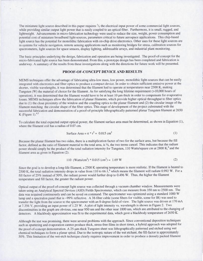
MEMS techniques offer the advantage of fabricating ultra- low mass, low power, monolithic light-sources that can be easi ly integrated with electronics and fiber optics to produce a compact device. In order to obtain suffic ient emissive power at the shorter, visib le wavelengths, it was determined that the fi lament had to operate at temperatures near 2500 K, making Tungsten (W) the material of choice for the filament. As for satisfying the long li feti me requirement (>10,000 hours of operation), it was determined that the fi lament wo uld have to be at least 10 /-lm thick in order to compensate for evaporative losses. MEMS techniques allow the fabr ication of planar fil aments, which provide higher optical throughput to fiber optics due to (1) the close proximity of the window and the coupling optics to the planar f il ament and (2) the circul ar image of the fila ment matching the circul ar shape of the fiber optics. This stage of development of the project culminated with the successfu l fabrication and demonstration of a proof-of-principle lithographically patterned planar Tungsten filament at 2650 K (Figure 1).4.5
To calculate the total expected output optical power, the filament surface area must be determined , as shown in Equation (1), where the fi lament co il has a radius of 0.07 cm.
Surface Area = 1[ * r2 = 0.015 cm2 (1)
Because the planar filament has two sides, there is a multiplication facto r of two for the surface area, but because the fi ll factor , defined as the ratio of filament material to the total area , is Yl, the two terms cancel. This indicates that the radiant power should simply be the product of the total radiation intensity for Tungsten, 110 Watts/square cm at 2800 K,6 and the filament area as given in Equation (2).
110 (Watts/cm2) * 0.015 (cm2) = 1.69 W (2)
Since the goal is to develop a long-life fil ament, a 2500 K operating temperature is more realistic. If the filament is heated to 2500 K, the total radiation intensity drops in value from 110 to 66.1,6 which means the fi lament wi ll radiate 0.992 W. For a fill factor of 25% instead of 50%, the radiant power would further drop to 0.496 W . Thus, the higher the fi lament temperature and fill facto r, the greater the radiant power.
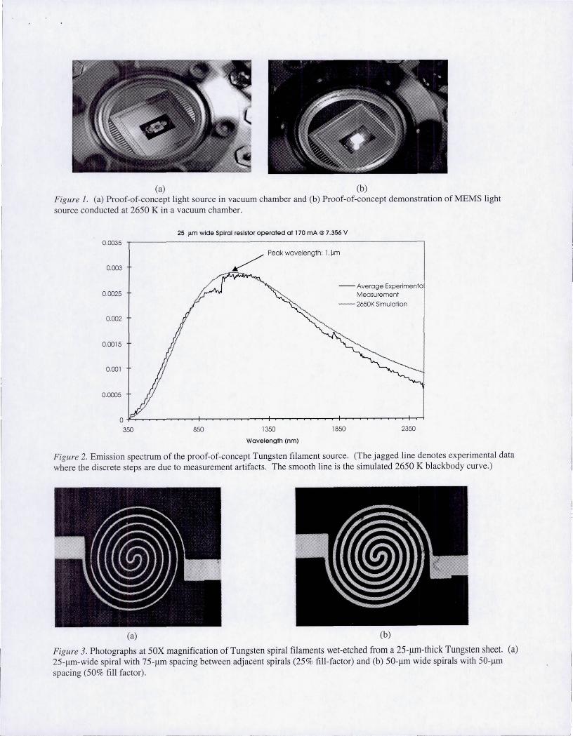
Optical output of the proof-of-concept light source was co ll ected through a vacuum chamber window. Measurements were taken using an Analytical Spectral Devices (ASD) Fie lds Spectrometer, which can measure fro m 350 nm to 2500 nm. The data was acquired continuously and can be saved on command. The spectrometer was optimized using a standard 1000 W lamp and a spectralon panel that is -99% reflective. A 38-fiber cable (some fibers for visible, some for IR) was used to transfer the light from the source to the spectrometer with an 8-degree field-of-view. The light source was driven at 170 rnA at 7.356 Y, providing an input power of l.25 W. A plot of light intensity vs. wavelength is shown in F igure 2. Two discontinuities in the graph are obvious, one near 950 nm and the other near 1800 nm, which are attr ibuted to the changing of detectors. A blackbody approxi mation was fit to the experimental data, which gave a blackbody temperature of 2650 K.
Although the test was promising, there were several problems with the approach. Since conventiona l deposition techniques such as sputtering and evaporation cannot produce thick, stress-free fi lms in short times, a hybrid approach was adopted for the proof-of-concept demonstration . A 25-/-lm-thick Tungsten sheet was lithographica ll y patterned and etched using wet chemical techniques to form a planar spiral. Due to the isotropic nature of the wet etchant, the fi ll-facto r is approximately 50%. This limitation of the wet-etch technique clearly requires improvement in order to produce a densely packed fi lament
(a) (b) Figure J. (a) Proof-of-concept light source in vacuum chamber and (b) Proof-of-concept demonstration of MEMS light source conducted at 2650 K in a vacuum chamber.
0.0035
0.003
0.0025
0.002
0.0015
0.001
0.0005
25 I'm wide Spiral resistor operated at 170 mA @ 7.356 V
/ Peak wavelength: 1.)un
--Average Experimenta Measurement
- - 2650K Simulation
o~~~~,-~,-~~~~~~~~~~~~~~,-~~~~~~~
350 850 1350
Wavelength (nm)
1850 2350
Figure 2. Emiss ion spectrum of the proof-of-concept Tungsten fi lament source. (The jagged line denotes experimental data where the discrete steps are due to measurement artifacts . The smooth line is the simulated 2650 K blackbody curve.)
(a) (b)
Figure 3. Photographs at 50X magnification of Tungsten spiral fila ments wet-etched from a 2S- )lm-thick Tungsten sheet. (a) 25-llm-wide spiral with 75-1lffi spacing between adjacent spirals (25% fill-factor) and (b) 50-1lffi wide spira ls with 50-11m spac ing (50% fi ll factor).
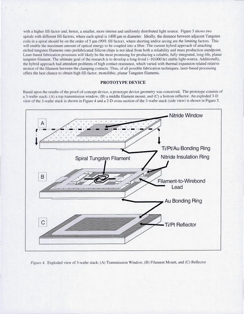
with a higher fi ll -factor and, hence, a smaller, more intense and uniforml y di stri buted light source. Figure 3 shows two spirals with different fill-factors, where each spiral is 1400 /lm in diameter. Ideally, the distance between adjacent Tungsten coils in a spiral should be on the order of 5 /lm (90% fill factor), where shorting and/or arcing are the limiti ng factors. This will enable the maximum amount of optical energy to be coupled into a fiber. The current hybrid approach of attach ing etched tungsten fi laments onto prefabricated Sil icon chi ps is not ideal from both a reliability and mass production standpoint. Laser-based fabrication processes will li kely be the most promising fo r producing a re li ab le, full y integrated, long-life, planar tungsten filament. The ulti mate goa l of the research is to develop a long-li ved (-10,000 hr) stable light-source. Add itionally, the hybrid approach had attendant problems of high contact resistance, which varied wi th thermal expansion related relative motion of the fi lament between the clamping contacts. Thus, of all poss ib le fa brication techniques, laser-based processi ng offers the best chance to obtain high fill-factor, monoli thic, planar Tungsten fi laments.
PROTOTYPE DEVICE
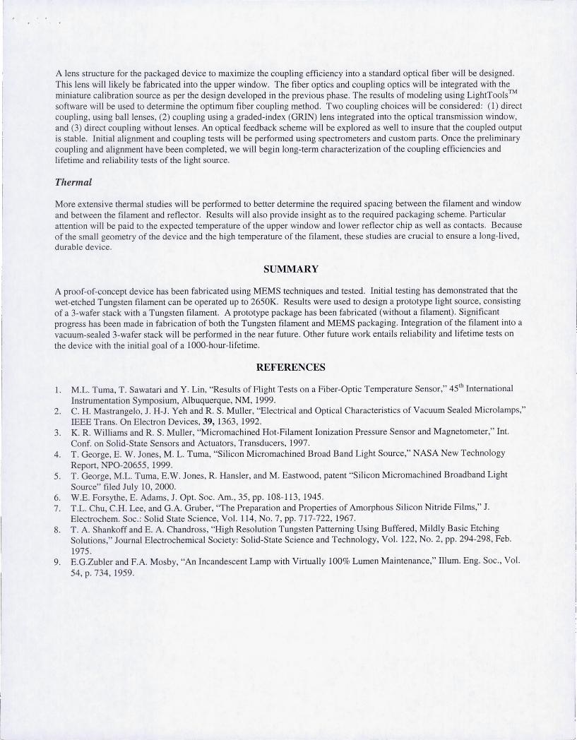
Based upon the resu lts of the proof-of-concept device, a prototype device geometry was conceived. The prototype consists of a 3-wafer stack: (A) a top transmission window, (B) a middle fi lament mount, and (C) a botto m refl ector. An exploded 3-D view of the 3-wafer stack is shown in Figure 4 and a 2-D cross-section of the 3-wafer stack (side view) is shown in Figure 5.
~ .. ~.-=-. ~ .. ~.~. ~ .. ::=::. =.~.;:. ~.~. ~.~~~;:~_ Nitride Window
11....-... II _ l.1
Ti/Pt/ Au Bonding Ring
Filament -to-Wi rebond Lead
--"""'---_..., Au Bonding Ring
~""-Ti/Pt Reflector
Figure 4. Exploded view of 3-wafer stack: (A) Transmission Window, (B) Filament Mount, and (C) Reflector

~---.-------,..---~------ Nitride Window
o Spiral Tungsten
Filament
o ________ TilPtiAu Bonding Ring
/ ~ Nitride Insulation Ring
c :::J-..... G~:L, ___ Filament-to-Wirebond Lead
Gold Wirebond to Package
TilPtiAu Bonding Ring
~_E_" ____________ ~----TilPt Reflector
Silicon
TilPt/Au
• Silicon Nitride • Tungsten Filament • Pt Reflector
Figure 5. Cross-section of 3-wafer stack along dotted line shown in F igw-e 4 . (A) Transmission window, (B) Fil ament mount, and (C) Refl ector.
The Sil icon substrates used to construct the 3-wafer stack are 400 11m in thi ckness . The phys ical dimensions of wafer B and Care 5.40 mm x 8.00 mm. Wafer A is 5.00 rnm x 7.20 mm to provide sufficient area on Wafer B for wire bonds and to prevent an electrical short between the two wafers. The outer dimensions of the 3-wafer stack are 5.4 mm x 8.0 mm x 1.2 mm. To test the prototype des ign, a packaged prototype has been fabricated, without the fil ament. The next step is to package a prototype with a fil ament enclosed.
A. Transmission Window Fabrication
The top substrate functions as a transmission window and is bonded to the middle substrate by Au/Au thermal compression bonding. Initiall y, a 1000A. PECVD low-stress Silicon Nitride film is deposited onto 400-J1m-thick bare Silicon. Silicon Nitride was chosen because it is opticall y transparent between 0.5 11m and 8 J1m .? A T ilPtiAu bonding ring (200/200/2000A.) is then evaporated onto the unpol ished side using a lift-off process. Finall y, the bottom Ni tride and the bulk Silicon are etched to reveal the top Nitride window. This opening is wider than the fil ament length (spiral diameter plus leads on both ends), al lowing the 25 J1m-th ick-fi lament mounted to the middle substrate (shown in B) to fit inside. A 500-J1ffi pyrex coverslip is being considered as an alternate materi al for the transmission window. Both pyrex and Nitride are transparent in the wavelength of interest (500-900 nm) as seen in the transmiss ion measurements (Figures 6 and 7). These measurements were taken using an Acton "SpectraPro 275" spectrometer and an incandescent source. Intensity measurements were made in two runs, one with the test window in front of the slit and another run without it. The ratio of the intensity measured during the two runs was calculated and plotted as the fraction of transmitted light. The transmjss ion data through the Silicon Ni tride window is osci ll atory due to interference in the th in membrane. Tills Silicon Nitr ide membrane, while integrated into the top substrate, is fragi le and may yield under the large pressure gradient created after vacuum packaging. A pyrex coverslip is more mechanically robust than a Silicon Nitride membrane, but requires more fabrication steps and adds thickness to the transmission wi ndow and the overall fi nal device. Fabrication of a pyrex window device can be accomplished by eliminating the Nitride deposition and bonding pyrex to Sili con anodically, or by depositing T ilPti Au bonding rings on the top of substrate A (without the top Nitride layer) and on the bottom of the pyrex fo r thermal compress ion bonding. The prototype

device design shown in F igures 4 and 5 has integrated Nitride membranes. Fabrication of pyrex-windowed devices is in progress.
B. Filament Mount Fabrication
The middle substrate provides a mount for the Tungsten filament, an electri cal conduit through the hermetica lly sealed wafer stack, and a pad for wire bonding to the external packaging. F irst, 1000 A of PECVD Silicon Nitride is deposited on a bare Silicon wafer. Then, two leads are evaporated in the radial direction to electrically connect the filament with the wire bond pads. Next, I 11m ofPECVD Silicon Nitride is deposited to insulate the leads . It is patterned in a ring and etched in a Fluorine-based reactive ion etch (RIE) which has been optimized to avoid etching the underlying lead appreciably. A TiJPtJAu ring (200/20012000 A) is evaporated onto the Nitride insu lation ring using a lift-off process. This ring wi ll align to the ring on the substrate above (substrate A) during thermal compression bonding. A TiJPtJAu ring (200/200/2000 A) is then deposited on the unpolished side using a lift-off process and functions as a bonding ring to the substrate below (substrate C). Finally, deep reactive-ion etching is used to etch a 3.9 x 2.9 mm hole through the entire Silicon wafer.
Filament Fabrication
Tungsten fi laments are fabricated fro m a 25- llm-thick Tungsten sheet. Photoresist is patterned on both sides of the sheet with the fi lament geometry, and the sheet is chemically etched from both sides in a K3Fe(CN)6 etch.s This was sufficient to etch the entire thickness of the sheet. Etching from both sides reduces lateral etching from 25 11m to 12.5 /lID and thereby improves the final device fi ll factor. Other methods such as laser etching are bei ng explored to further improve fi lament fi ll factor.
c. Reflector Fabrication
The bottom reflector provides a reflective surface to improve transmission through the transmission window above by reflecting a portion of the bottom filament radiation to the window. It is fabricated by evaporating a TiJPt (20011000 A) reflective film onto a bare Silicon wafer. A TiJPtJAu ring (200120012000 A) is then evaporated onto the reflective layer for thermal compression bonding to the middle substrate. In future devices, Silver (Ag) will be used as the reflective surface as it is more highly reflective than Pt over the visible-IR wavelength region.
Assembly and Packaging
The substrates are individually diced after the fabrication steps described above have been performed. The filament is attached to the middle substrate by two Gold ribbons. Other methods of fi lament attachment such as thermal compression bonding or Au eutectic bonding are presently being explored . Finally, the entire stack is bonded in a thermal compression bonder. To ensure hermetic sealing, the bonding step is performed in an evacuated chamber « 10-6 Torr), or a backfilled chamber of either pure or halogen-doped N2. To avoid damaging the fragile Silicon Nitride window, a flat pyrex piece, approximately the same size as substrate A, is placed on substrate A and a graphite piece is placed on top of the pyrex to protect the device against surface roughness in the compression bonder piston. Once the 3-wafer stack wi th filament is assembled, wire bonds are used to connect the stack to a more robust ceramic package.
The transmission through the upper pyrex window and Silicon Nitride window were measured experimentally as described in section A above. Results from the measurements are shown in Figures 6 and 7. A di fferent material, such as sapphire, would be chosen for the window if one were also interested in usi ng the infrared (IR) portion of the wavelength spectrum. Thus, by changing the optical window, one can tailor the output optical spectrum to a particul ar application.
FUTURE WORK
Device Fabrication and Packaging
Packaging studies with filaments processed using the wet-etch technique will begin shortly. The two critical packaging issues are filament attachment and device seal wi th different ambient gases. Ideally, resisti ve heating should only occur at the filament itself. However, results from the proof-of-concept device indicate that the contact resistance of the filament and bond pad junctions can be high during fi lament operation due to thermal expansion of the fi lament. The proof-of-concept hybrid-filament was attached using a rather crude, Gold strap bonding technique using a ribbon bonder. Two different approaches have been taken to lower contact resistance: spot welding and eutectic bonding. The second issue, device seal,

- --_. -_ . ~- .
directly impacts the lifetime of the fi lament. The ambient inside the sea led device must be free of oxygen and water vapor, which can quickly oxidize the hot filament. A sealing chamber will be built that can be pressurized with the appropriate gas . The ambient environments currently under consideration are vacuum, njtrogen, and halogen-doped njtrogen. Halogen doping addresses the issue of Tungsten condensation onto the window during operation, which will decrease transmjssion over time. The halo?en will set in motion a chemica l reacti on cycle that will remove the Tungsten off the window and redeposit it on the filament.
Transmission Through Glass Window
~ 0.8
c .~ .§
0.6
VI c 0.4 E r
0.2
0
300 400 500 600 700 800 900
Wavelength (nm)
Figure 6. Optical transmission through pyrex window chip vs. wavelength.
Transmission Through Silicon itride Window
0.8 c 0
' 0;; 0.6 VI
.~ c 0.4 E! r
0.2
0
300 400 500 600 700 800 900
Wavelength (nm)
Figure 7. Optical transmission through Silicon Nitride window vs. wavelength.
Fiber optic coupling and testing
One of the goals of this project is to effic iently couple the output of the device into an optical fi ber. Computer modeling of the device wi ll be performed to determine the optimum coupling technique. Results will allow for the addition of fiber coupling into the device design. When a Tungsten filament is heated for the fust time, there is a tendency for it to di tort slightly due to grain growth and the forces from thermal expansion. This may cause part of the planar fi lament to move in or out of plane. If the filament is coupled to the fiber by a normal two-ball lens system, a small change in the position of the source will be imaged as a small change in the image position. Because the image of the filament is considerably larger than the core of the fiber, this movement will have negligible effect on the amount of light entering the fi ber. Thus, we expect stable coupling efficiency of the output power of this device. If the structure is set before the optics are assembled, any distortion in the filament may be corrected by the placement of the optics.
-----_ ....... _-
A lens structure for the packaged device to maximize the coupl ing efficiency into a standard optical fiber will be designed . This lens will likely be fabricated into the upper window. The fiber optics and coupli ng optics will be integrated with the miniature calibration source as per the design developed in the previous phase. The resu lts of modeling using LightTools™ software will be used to determine the optimum fiber coupling method. Two coupling cho ices will be considered: (1) direct coupling, using ball lenses, (2) coupling using a graded-index (GRIN) lens integrated into the optica l tra nsmission window, and (3) di.rect coupling without lenses. An optical feedback scbeme will be explored as well to insure that the coupled output is stab le. Initia l alignment and coupli ng tests will be perfo rmed usi ng spectrometers and custom parts. Once the preliminary coupling and alignment have been completed, we wi ll begin long-term characterization of the coupling efficiencies and lifetime and reliability tests of the light source.
Thermal
More extensive thermal studies will be performed to better determine the required spaci ng between the f il ament and window and between the fi lament and reflector. Results will also provide insight as to the required packaging scheme. Particu lar attention wi ll be paid to the expected temperature of the upper window and lower reflector chip as well as contacts. Because of the small geometry of the device and the high temperature of the fi lament, these studies are cruc ial to ensure a long-lived, durable device.
SUMMARY
A proof-of-concept device has been fabricated using MEMS techniques and tested. Initi al testing has demonstrated that the wet-etched Tungsten filament can be operated up to 2650K. Results were used to design a prototype light source, consisting of a 3-wafer stack with a Tungsten fi lament. A prototype package has been fabricated (without a fi lament). Significant progress has been made in fabricat ion of both the Tungsten fil ament and MEMS packaging. Integration of the filament into a vacuum-sealed 3-wafer stack wi ll be performed in the near future . Other future work entail s re li abi lity and lifetime tests on the device with the initial goal of a 1000-hour-lifetime.
REFERENCES
1. M.L. Tuma, T. Sawatari and Y. Lin, "Results of F light Tests on a Fiber-Optic Temperature Sensor," 45 th International Instrumentation Symposium, Albuquerque, NM, 1999.
2. C. H. Mastrangelo, J. H-J. Yeh and R . S. Muller, "Electrica l and Optical Characteristics of Vacuum Sealed Microlamps," IEEE Trans. On Electron Devices , 39, 1363, 1992.
3. K. R Williams and R S. Muller, "Micromachined Hot-Filament Ionization Pressure Sensor and Magnetometer," Int. Cont. on Solid-State Sensors and Actuators, Transducers, 1997.
4. T. George, E. W. Jones, M . L. Tuma, "Silicon Micromachined Broad Band Light Source," NASA New Technology Report, NPO-20655, 1999.
5. T. George, M.L. Tuma, E.W. Jones, R Hansler, and M. Eastwood, patent "Silicon Micromachined Broadband Light Source" filed July 10,2000.
6. W .E . Forsythe, E. Adams, J. Opt. Soc. Am., 35, pp. 108-113, 1945. 7 . T.L. Chu, C.H. Lee, and G.A. Gruber, ''The Preparation and Properties of Amorphous S ili con Nitride Films," 1.
Electrochem. Soc.: Solid State Science, Vol. 114, No. 7, pp. 717-722, 1967. 8. T . A. Shankoff and E. A. Chandross, "High Reso lution Tungsten Patterning Using Buffered, Mildly Basic Etchi ng
Solutions," Journal Electrochemical Society: Solid-State Science and Technology, Vol. 122, No.2, pp. 294-298, Feb. 1975.
9. E.G.Zubler and FA. Mosby, "An Incandescent Lamp with Virtually 100% Lumen Maintenance," IlIum. Eng. Soc., Vol. 54, p. 734, 1959.