memory in embedded systemscseweb.ucsd.edu/classes/wi16/cse237a-a/handouts/03.mem.pdfmemory in...
TRANSCRIPT

Memory in Embedded Systems
Tajana Simunic Rosing
Department of Computer Science and Engineering
University of California, San Diego.

Hardware platform architecture

Traditional Memory Hierarchies

Embedded memory hierarchy
• Registers– Very fast, next to ALU,
power hungy
• Cache– Small, expensive, fast
memory stores a copy of likely accessed parts
– L1, L2, L3
• Predictability– Scratchpad memory
• Main memory– Large, inexpensive, slower
• Permanence– Non-volatile memories
Processor
Cache
Main memory
SSD
Disk & Backup (Black box)
Registers

Caches and CPUs
• Servers: L1,L2 &L3 cache on chip
• Embedded: L1, L2 on chip
Raspberry PI 2Server
Cache
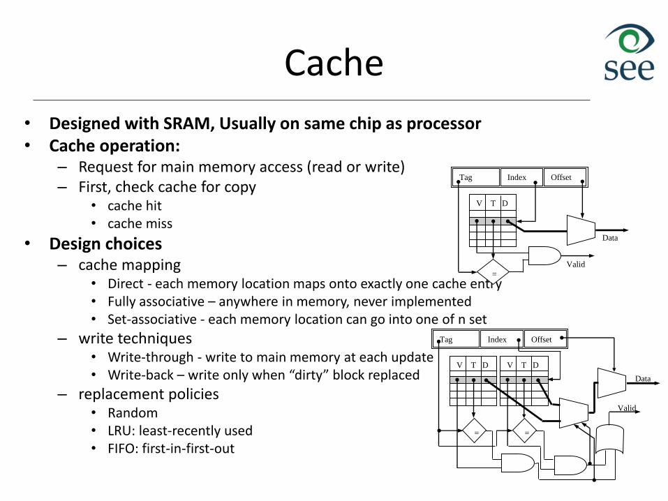
• Designed with SRAM, Usually on same chip as processor• Cache operation:
– Request for main memory access (read or write)– First, check cache for copy
• cache hit• cache miss
• Design choices– cache mapping
• Direct - each memory location maps onto exactly one cache entry• Fully associative – anywhere in memory, never implemented• Set-associative - each memory location can go into one of n set
– write techniques• Write-through - write to main memory at each update• Write-back – write only when “dirty” block replaced
– replacement policies• Random• LRU: least-recently used• FIFO: first-in-first-out
Data
Valid
Tag Index Offset
=
V T D
Tag Index Offset
=
V T D
Data
Valid
V T D
=
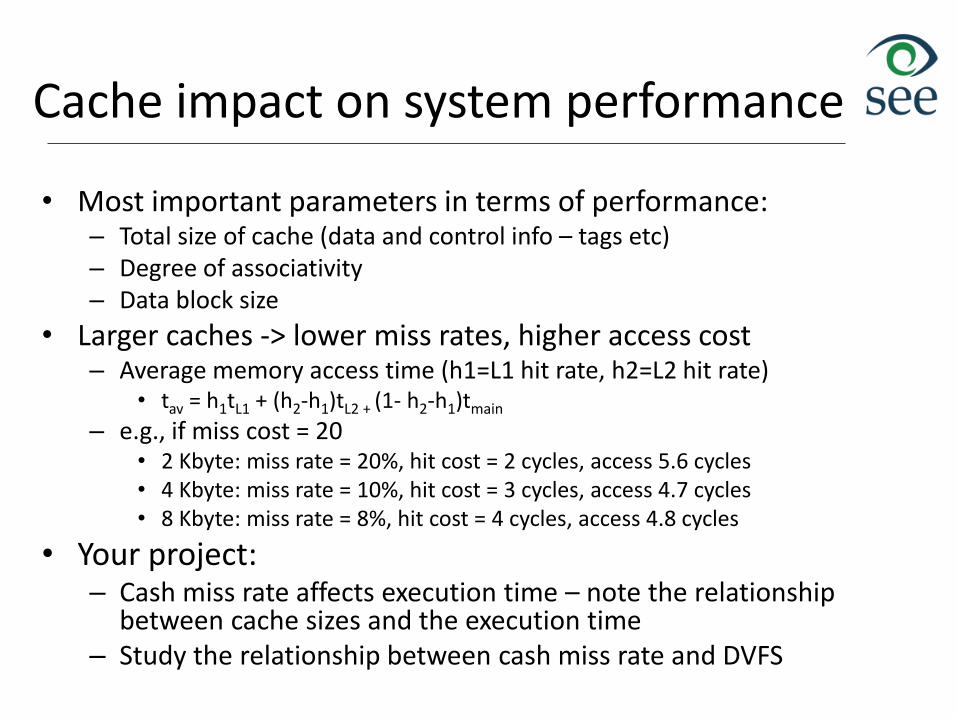
Cache impact on system performance
• Most important parameters in terms of performance:– Total size of cache (data and control info – tags etc)– Degree of associativity– Data block size
• Larger caches -> lower miss rates, higher access cost– Average memory access time (h1=L1 hit rate, h2=L2 hit rate)
• tav = h1tL1 + (h2-h1)tL2 + (1- h2-h1)tmain
– e.g., if miss cost = 20 • 2 Kbyte: miss rate = 20%, hit cost = 2 cycles, access 5.6 cycles• 4 Kbyte: miss rate = 10%, hit cost = 3 cycles, access 4.7 cycles• 8 Kbyte: miss rate = 8%, hit cost = 4 cycles, access 4.8 cycles
• Your project:– Cash miss rate affects execution time – note the relationship
between cache sizes and the execution time– Study the relationship between cash miss rate and DVFS

Predictability
• Embedded systems are often real-time:
– Have to guarantee meeting timing constraints.
• Pre run-time scheduling - predictability
Time-triggered, statically scheduled operating systems
Predictable cache design?

Scratch pad memories (SPM)
• Address space
ARM7TDMI
well-known for
low power
consumptionscratch pad memory
0
FFF..
main
SPM
processor
Hierarchy
Example
no tag
memory
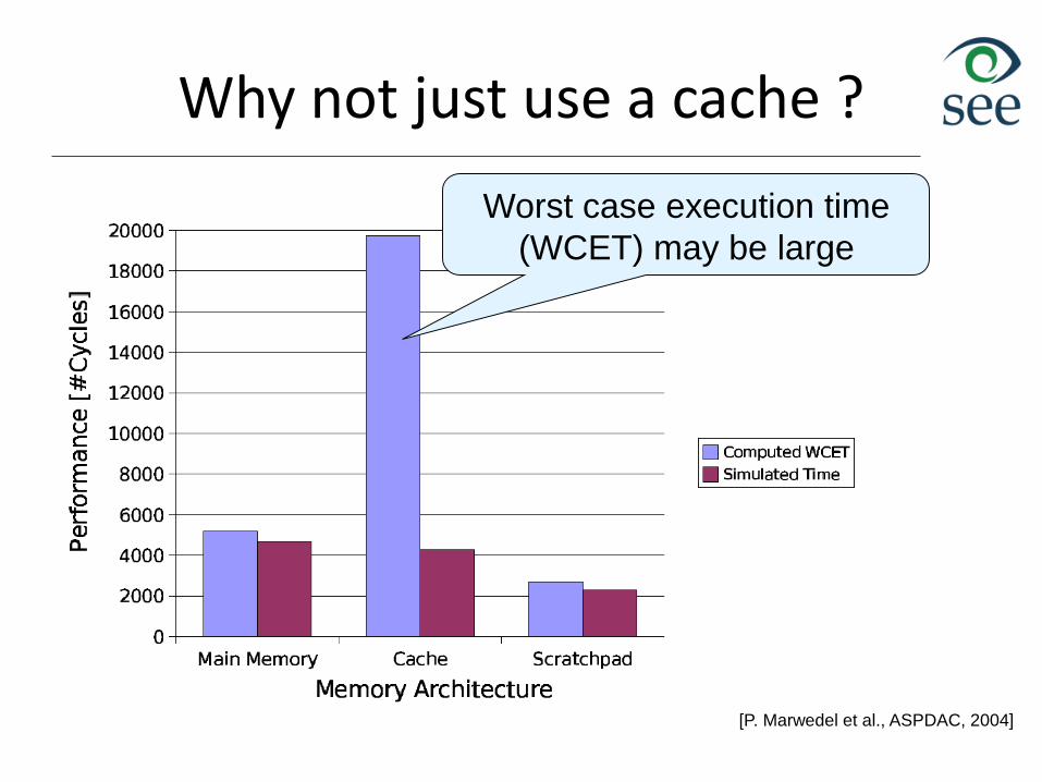
Why not just use a cache ?
[P. Marwedel et al., ASPDAC, 2004]
Worst case execution time
(WCET) may be large

ARM memory hierarchy
Tightly coupled memory = Scratchpad!
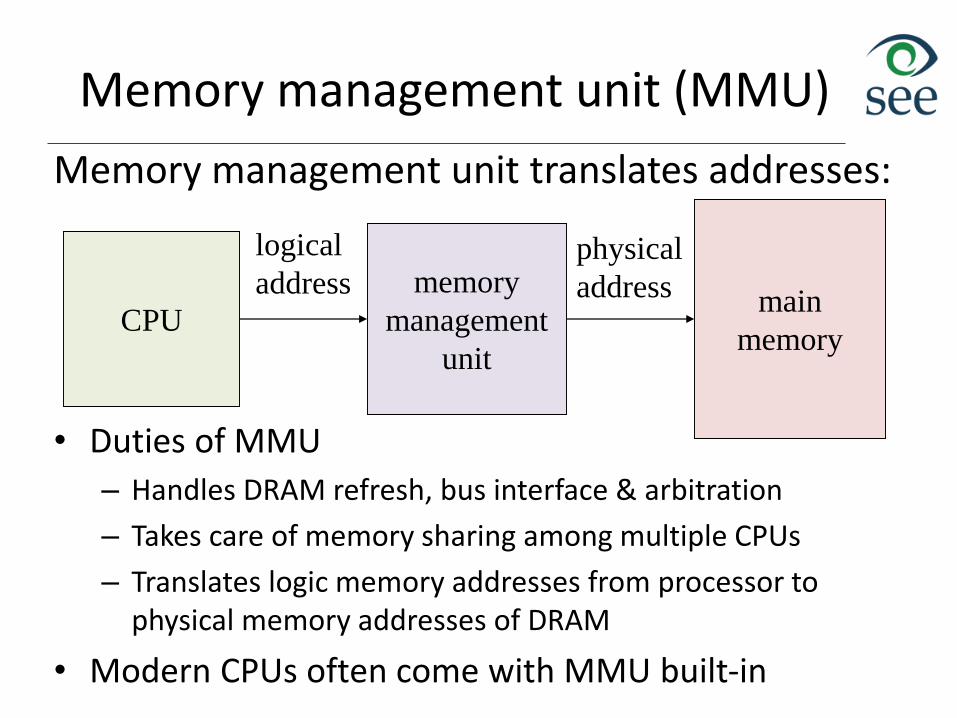
Memory management unit (MMU)
Memory management unit translates addresses:
CPUmain
memory
memory
management
unit
logical
addressphysical
address
• Duties of MMU
– Handles DRAM refresh, bus interface & arbitration
– Takes care of memory sharing among multiple CPUs
– Translates logic memory addresses from processor to physical memory addresses of DRAM
• Modern CPUs often come with MMU built-in

Address translation
• Mapping logical to physical addresses
• Two basic schemes:– Segmented
• memory footprint can change dynamically
• usually only a few segments per process; e.g. data and stack
– Paged• size preassigned
– can be combined (x86)
SEGMENTATION PAGING
Involves programmer Transparent to programmer
Separate compiling No separate compiling
Separate protection No separate protection
Shared No sharing
memory
segment 1
segment 2
page 1page 2

ARM memory management
• Memory region types:
– section: 1 MB block
– large (64KB) & small (4KB) pages
• Address is marked as section or page-mapped
• Two-level translation scheme

ARM address translation
offset1st index 2nd index
physical address
Translation table
base register
1st level tabledescriptor
2nd level tabledescriptor
concatenate
concatenate

Volatile Memory
• Register file – Fastest
– But biggest size – built from D-FFs
• SRAM: Static RAM– Memory cell uses flip-flop to store bit– Requires 6 transistors – Holds data as long as power supplied
• DRAM: Dynamic RAM– Memory cell uses MOS transistor and capacitor to
store a bit– More compact than SRAM– “Refresh” required due to capacitor leak
• word’s cells refreshed when read
– Typical refresh rate 15.625 microsec.– Slower to access than SRAM
Data
W
Data'
SRAM
Data
W
DRAM
R S R S R S
D Q D Q D Q D Q
OUT1 OUT2 OUT3 OUT4
CLK
IN1 IN2 IN3 IN4
R S

RAM organization
• Stores large number of bits
– m x n: m words of n bits each
– k = Log2(m) address input signals
– or m = 2^k words
– e.g., 4,096 x 8 memory:
• 32,768 bits
• 12 address input signals
• 8 input/output data signals
• Memory access
– r/w: selects read or write
– enable: read or write only when asserted
– multiport: multiple accesses to different locations simultaneously
m n memory
…
…
n bits per word
mw
ord
s
enable
2k n read and write
memory
A0…
r/w
…
Q0Qn-1
Ak-1
memory external view
4 4 RAM
2 4
decoder
Q0Q3
A0
enable
A1
Q2 Q1
Memory
cell
I0I3 I2 I1
rd/wr To every cell
internal view
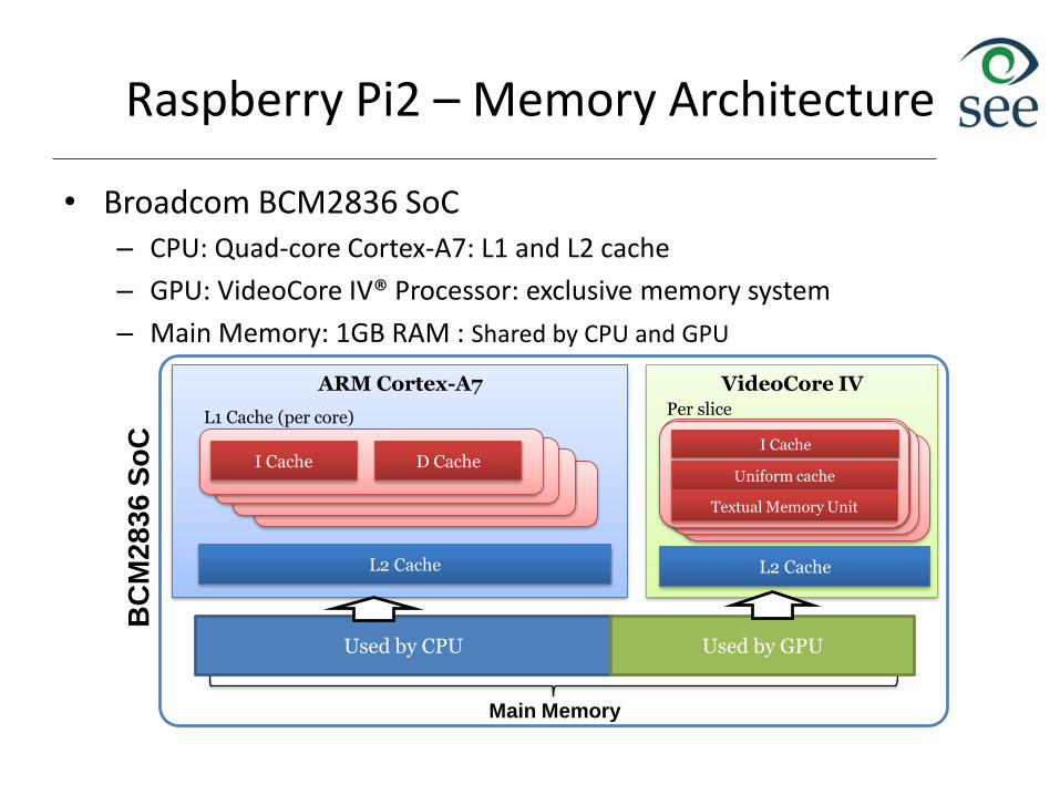
Raspberry Pi2 – Memory Architecture
• Broadcom BCM2836 SoC– CPU: Quad-core Cortex-A7: L1 and L2 cache
– GPU: VideoCore IV® Processor: exclusive memory system
– Main Memory: 1GB RAM : Shared by CPU and GPU
VideoCore IVARM Cortex-A7
Used by CPU Used by GPU
L2 Cache
I Cache D Cache
L1 Cache (per core)
Main Memory
L2 Cache
I Cache
Uniform cache
Textual Memory Unit
Per slice
BC
M2
83
6 S
oC

Cortex-A7 Memory: L1 Cache
• 32KB L1 Cache
– Instruction Cache (I-Cache)
• 32-bytes cache line
• 2-way set-associative
– Data Cache (D-Cache)
• 64-bytes cache line
• 4-way set-associative
– Pseudo random cache replacement
• Data Cache Unit (DCU): Contains a controller for MOESI protocol in processor
– M (Modified): The line is only in this cache and is dirty.
– O (Owned): The line is possibly in more than one cache and is dirty.
– E (Exclusive):The line is only in this cache and is clean.
– S (Shared): The line is possibly in more than one cache and is clean
– I (Invalid): The line is not in this cache.
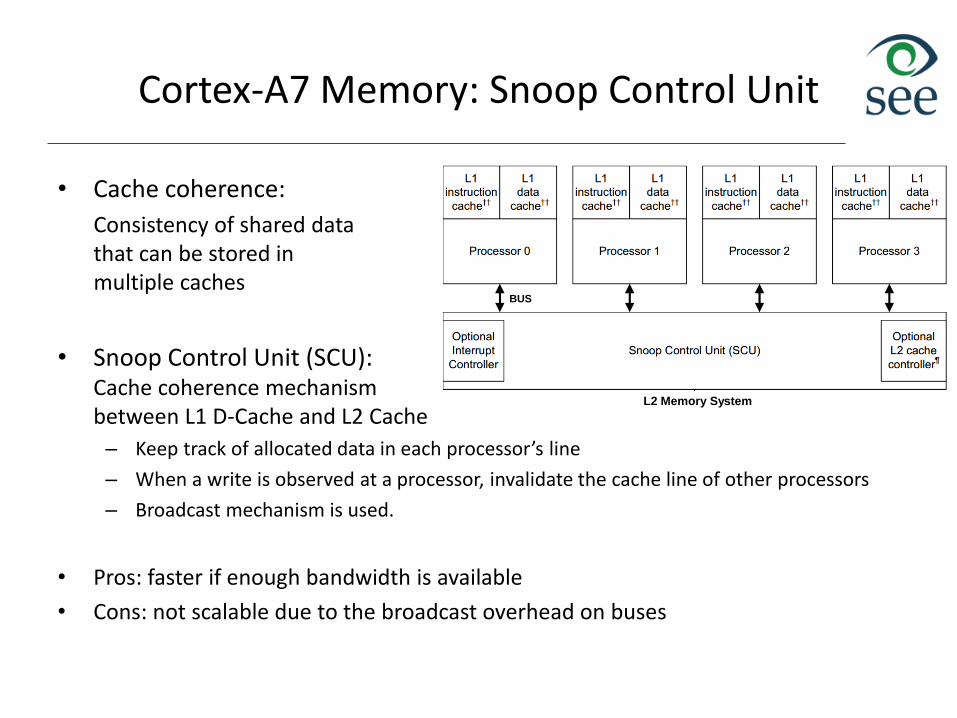
Cortex-A7 Memory: Snoop Control Unit
• Cache coherence:
Consistency of shared datathat can be stored inmultiple caches
• Snoop Control Unit (SCU):Cache coherence mechanismbetween L1 D-Cache and L2 Cache
– Keep track of allocated data in each processor’s line
– When a write is observed at a processor, invalidate the cache line of other processors
– Broadcast mechanism is used.
• Pros: faster if enough bandwidth is available
• Cons: not scalable due to the broadcast overhead on buses
L2 Memory System
BUS

VideoCore 4 (GPU) Memory• Specialized to accelerate
3D/multimedia data
• Vertex Pipe Memory(VPM):
– A type of cache, it is shared & system-wide
– performs DMA from main memory to read/write vertex data
• L2 Cache: shared by all slices
• Per-slice memory
– Icache: instruction cache
– Uniforms Cache:Stores a stream of data
– Texture and Memory Lookup Unit (TMU):
• Stores general-purpose data and textures
• FIFO-based texture lookup

Raspberry Pi2- Main Memory (RAM)
• Divided in ARM Cortex-7 and VideoCore 4 components
– Partially shared (e.g. frame buffer)
• Kernel is loaded from 0x8000 (32KB)
• Local peripherals:Reserved memory area for
– ARM timer: 64-bit timing signal
– IRQs (Interrupt Requests) to cores
– Mailbox (part of local perhipherals)memory area to facilitatecommunication betweenARM and VideoCore
1. Write data to the mailbox2. Issue special Interrupts to either ARM core or VideoCore
Local peripherals0x4001_FFFF
SD RAM ARM
SD RAM VC
DMA, GPIO,
PCM, etc

Raspberry Pi2-MMU
– Cortex-A7: Extended VMSAv7 MMU• ARMv7-A virtual memory system architecture
• Security extension
• Virtualization extension
• Large physical address extension
– Uses 2 Level TLBs
• L1 MMU
– 2 micro TLBs:I-cache (IuTLB) and D-cache (DuTLB)
– 10 entry full-associative
• L2 MMU
– A unified TLB
– 256 entry 2-way set-assoc.

Non-volatile memory
• A new class of data storage/memory devices
• Emerging NVMs have exciting features:
– Non-volatile like Flash ( ~ 10 years)
– Fast access times (~ SRAM)
– High density (~ DRAM)
• NVM blurs the distinction between
– MEMORY (fast, expensive, volatile ) and
– STORAGE (slow, cheap, non-volatile)
• Key issues:
– Slow writes, low endurance, costly and complex manufacturing

Older NVMs• Mask or fuse programmed ROM
• Erasable Programmable ROM (EPROM)– Uses “floating-gate transistor” in each cell
– Programmer uses higher-than-normal voltage so electrons tunnel into the gate• Electrons become trapped in the gate
• Only done for cells that should store 0
• Other cells will be 1
– To erase, shine ultraviolet light onto chip• Gives trapped electrons energy to escape
• Requires chip package to have window
• Electronically-Erasable Programmable ROM (EEPROM)– Erasing one word at a time electronically
• Flash memory– Like EEPROM, but large blocks of words can be
erased simultaneously
• EEPROM & FLASH are in-system programmable
cell cell
wordenable
data line data line
eÐeÐ
trapped electrons
01
flo
atin
g-g
ate
tra
nsis
tor
32
10data
addr
en
write
busy
1024x32EEPROM

STT-RAM: Spin-Transfer Torque RAM
• The spin torque direction of electrons to flip a bit in a magnetic tunneling junction (MTJ)
(a) The Structure of MTJ
(b) Parallel: bit 0 (low Resistance)
(c) Anti-Parallel: bit 1 (high Resistance)
• Advantage:
• High endurance
• Disadvantages:
• Write energy: High amount of current needed to reorient the magnetization for most commercial applications.;
• Write latency: Low ON/OFF resistance ratio (~2); Low
• Asymmetric write: Writing “1s” needs much more time and energy than writing zero
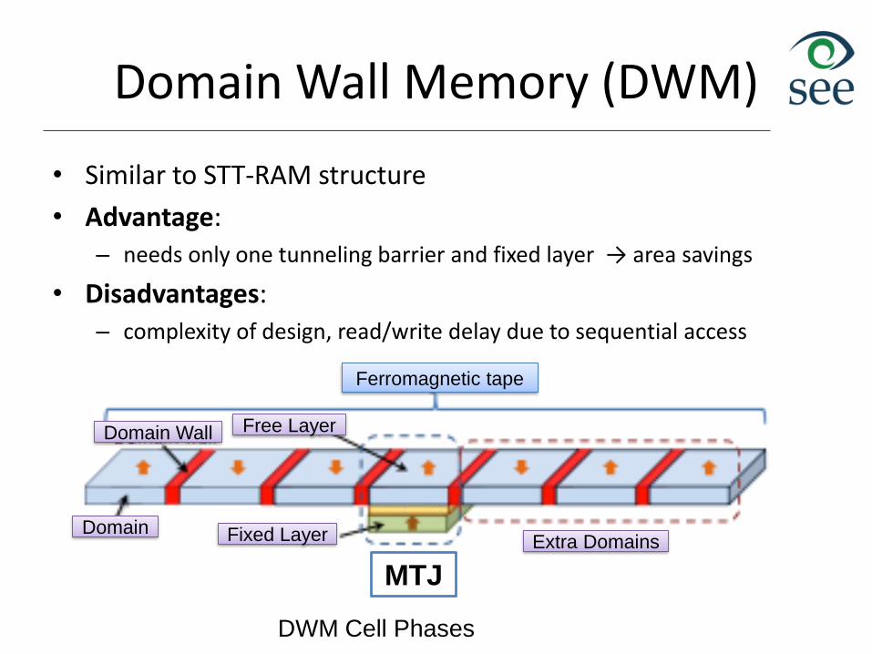
Domain Wall Memory (DWM)
• Similar to STT-RAM structure
• Advantage: – needs only one tunneling barrier and fixed layer → area savings
• Disadvantages: – complexity of design, read/write delay due to sequential access
Ferromagnetic tape
Free LayerDomain Wall
Domain Fixed Layer Extra Domains
MTJ
DWM Cell Phases

Shift-based DWM
• Writes by shifting data of one of the two fixed layers with the desirable direction comp
• Advantage: Faster writes than a traditional DWM
• Disadvantage: cost and manufacturing complexity
(a) 1-bit DWM Fast (b) Multi-bit DWM Area efficient,
but needs extra latency for shifting
28
Polarized direction

ReRAM: Resistive RAM
• Two types: access-based and crossbar ReRAM
• Access-based transistor (1T-1R)
– A dielectric, which is normally insulating, can conduct when exposed to sufficiently high voltage
• Crossbar (1T-nR)
– Resistance on top of the chip, and only transistor in silicon (3D arch)
– Highly scalable
– Very low energy consumption
Working mechanism of ReRAM

ReRAM: Resistive RAM
• Advantages:– Potentially a strong candidate to replace with NAND flash,
approximate computing, neuromorphic computing
– Very fast for both reads and writes
• Disadvantage: – Limited endurance
Crossbar ReRAM

PCM: Phase Change Memory
Phase Change Memory (PCM)– Flips a bit by changing the state of material
– Crystalline (SET) and amorphous (RESET) phase
PCM Cell Phases
PCM Operation
Advantages: – better scalability than other
emerging technologies.
– Good candidate for main memory replacement
Disadvantages: – Slow in write (non-symmetric write
operation)
– Low endurance (107)

Active vs Passive Power• The blue area marks active power in the
power equations
• The red area marks passive power in the power equations
– Passive power is unproductive. It just causes heat
– For memories it is leakage and refresh power, which is typically smaller than maximum active power
– For disks it is keeping the motor spinning and the standby power of the electronics, which is typically larger than the maximum active power
– For PCM it is the leakage and small standby power and is typically much smaller than the maximum active power.
fCVIVIVP ddDRAM dddd
2
refreshleak
VIVIrdPDisk t&sc&i
8.26.4
ddddPCM VIVIP activestandby
passive active
motordisk theofpower normalized theis
productive and active is device that the timeofportion theis

NVRAM Comparison
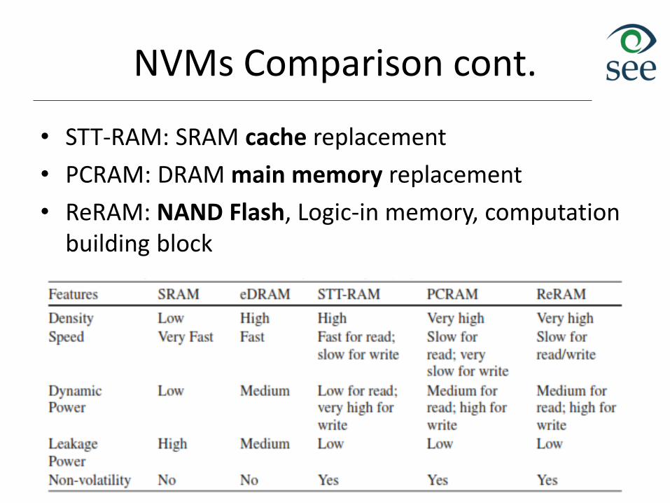
NVMs Comparison cont.
• STT-RAM: SRAM cache replacement
• PCRAM: DRAM main memory replacement
• ReRAM: NAND Flash, Logic-in memory, computation building block

Summary
• Memory hierarchy
– Needs: speed, low power, predictable
• Cache design
– Mapping, replacement & write policies
• Memory types
– ROM vs RAM, types of ROM/RAM
• NVM
– Many new technologies that are still maturing

Sources and References
• Frank Vahid, Tony Givargis, “Embedded System Design,” Wiley, 2002.
• Wayne Wolf, “Computers as Components,” Morgan Kaufmann, 2001.
• Peter Marwedel, “Embedded Systems Design,” 2004.

Phase-change
RAM
Access device(transistor, diode)
PCRAM“programmable
resistor”
Bit-line
Word-line
temperature
time
Tmelt
Tcryst
“RESET” pulse
“SET” pulse
Voltage
Potential headache:
High power/current affects scaling!
Potential headache:
If crystallization is slow affects performance!