megamacs to teramacs: implementing digital signal ... dsp applications & signal processing...
TRANSCRIPT

© 2004 Altera Corporation© 2004 Altera Corporation
MegaMACs to TeraMACs: MegaMACs to TeraMACs: Implementing Digital Implementing Digital Signal Processing (DSP)Signal Processing (DSP)in in FPGAsFPGAs
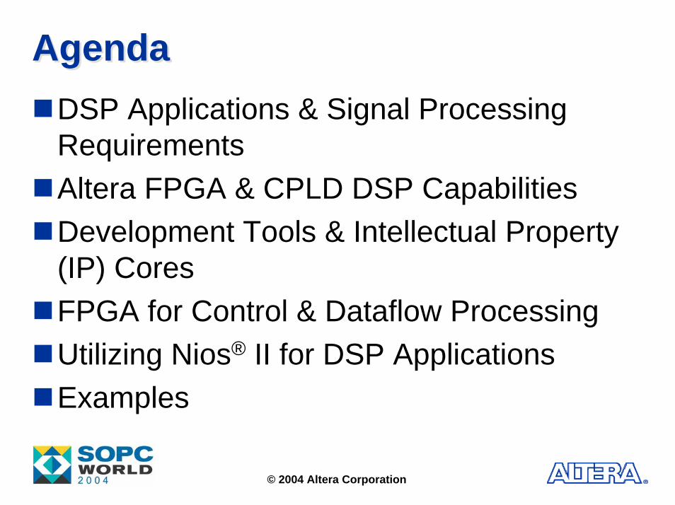
AgendaAgendaDSP Applications & Signal Processing RequirementsAltera FPGA & CPLD DSP CapabilitiesDevelopment Tools & Intellectual Property (IP) CoresFPGA for Control & Dataflow ProcessingUtilizing Nios® II for DSP ApplicationsExamples
© 2004 Altera Corporation

© 2004 Altera Corporation© 2004 Altera Corporation
DSP Applications & DSP Applications & Signal Processing Signal Processing RequirementsRequirements
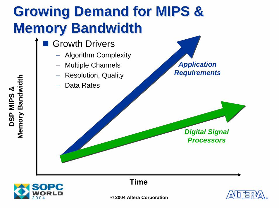
Growing Demand for MIPS &Memory BandwidthGrowing Demand for MIPS &Memory Bandwidth
Growth Drivers− Algorithm Complexity− Multiple Channels− Resolution, Quality− Data Rates
DSP
MIP
S &
Mem
ory
Ban
dwid
th
ApplicationRequirements
Digital SignalProcessors
© 2004 Altera Corporation
Time
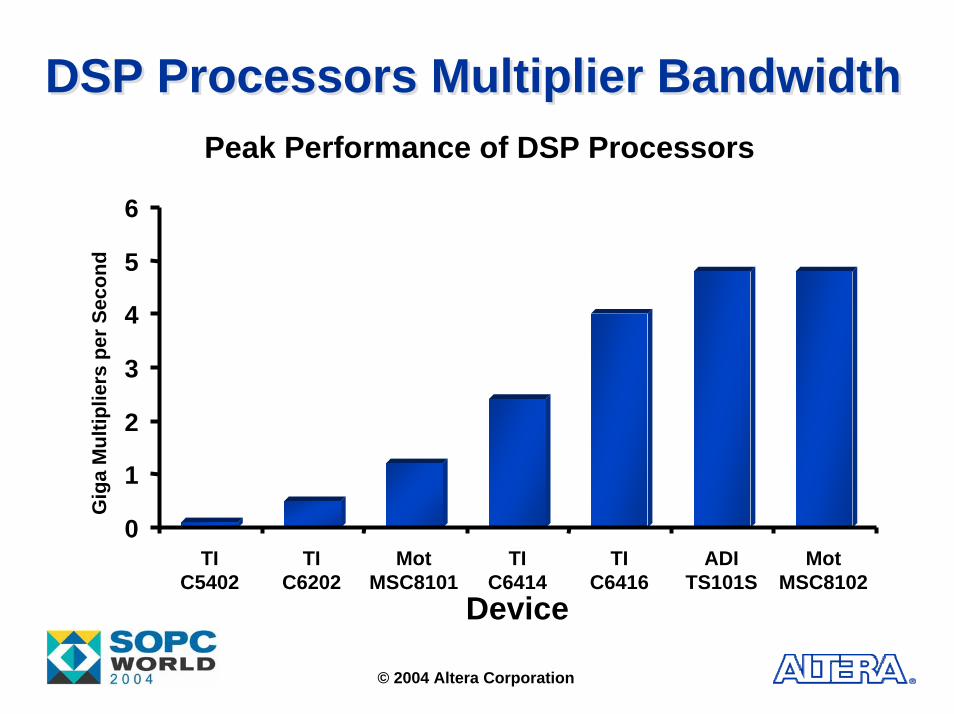
DSP Processors Multiplier BandwidthDSP Processors Multiplier BandwidthPeak Performance of DSP Processors
0
1
2
3
4
5
6
TIC5402
TIC6202
MotMSC8101
TIC6414
TIC6416
ADITS101S
MotMSC8102
Device
Gig
a M
ultip
liers
per
Sec
ond
© 2004 Altera Corporation

Embedded Multiplier Comparison with DSPsEmbedded Multiplier Comparison with DSPs
Note: Additional Multiplier Bandwidth Available Using Memory & Logic Elements (LEs)Stratix® II Bandwidth > 600 Giga Multiplies per Second
Altera® FPGAsDigital Signal Processors Giga Multiplies/s = Clock Frequency * # of 16x16 Hardware Multiplies
0
20
40
60
80
100
120
140
160
ADI TS203S TI C6416 TI C6410 AlteraEP2C20
AlteraEP2S60
AlteraEP2S180
40 GMACS40 GMACS
© 2004 Altera Corporation

Embedded Mega Multiplies/$Embedded Mega Multiplies/$
0
50
100
150
200
250
300
350
400
ADI TS203S TI C6410 MotorolaMSC7110
Altera EP2C20
Altera EP2S60
Based on the following 10k List Prices: TS203S ($35), C6410 ($18), MSC7110 ($12), EP2C20 ($15), EP2S60 ($150)
© 2004 Altera Corporation
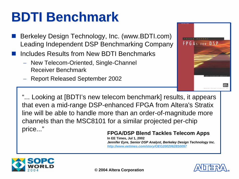
BDTI BenchmarkBDTI BenchmarkBerkeley Design Technology, Inc. (www.BDTI.com) Leading Independent DSP Benchmarking CompanyIncludes Results from New BDTI Benchmarks− New Telecom-Oriented, Single-Channel
Receiver Benchmark− Report Released September 2002
“... Looking at [BDTI’s new telecom benchmark] results, it appears that even a mid-range DSP-enhanced FPGA from Altera's Stratix line will be able to handle more than an order-of-magnitude more channels than the MSC8101 for a similar projected per-chip price...” FPGA/DSP Blend Tackles Telecom Apps
In EE Times, Jul 1, 2002Jennifer Eyre, Senior DSP Analyst, Berkeley Design Technology Inc.http://www.eetimes.com/story/OEG20020628S0097
© 2004 Altera Corporation

FPGA Growth for DSP: 26% Compound Annual Growth RateFPGA Growth for DSP: 26% Compound Annual Growth Rate
$0
$200
$400
$600
$800
$1,000
2002 2003 2004 2005 2006 2007
FPGA/PLD for DSP
Reconfigurable Devices for DSP
Shi
pmen
ts ($
Mill
ions
)
Mix Between Communications & Video & Image Processing
Source: 2004 Forward Concepts
© 2004 Altera Corporation

Altera’s Industry-Leading ComponentsAltera’s Industry-Leading Components
The Lowest-Cost CPLDs Ever
The Lowest-Cost FPGAs Ever
The Biggest & Fastest FPGAs Ever
The Industry’s Only Low-Cost, Comprehensive ASIC Alternative
© 2004 Altera Corporation

Altera’s Components Applied To DSPAltera’s Components Applied To DSPSmall DSP Tasks Encryption, Forward-Error Correction (FEC), Small Filtering
Low-Cost DSP PerformanceReplaces 1 or More DSP Processors
Industry’s Highest Performance Programmable DSP ProcessingReplaces Arrays of DSPs & ASICs
DSP Structured ASIC Solution
© 2004 Altera Corporation
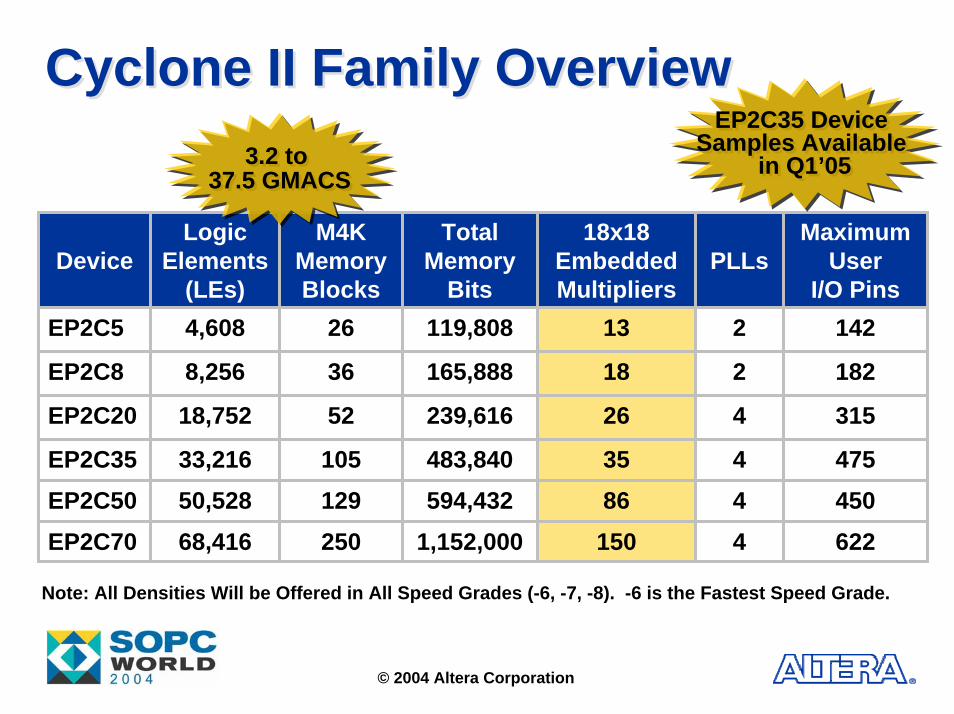
Cyclone II Family OverviewCyclone II Family Overview
DeviceLogic
Elements(LEs)
M4K MemoryBlocks
Total Memory
Bits
18x18 Embedded Multipliers
EP2C5 119,808
165,888
239,616
483,840594,432
1,152,000
EP2C8
13
18
26
3586
EP2C20
EP2C35EP2C50 50,528 129 4 450
150EP2C70
PLLs
26 2
2
4
4
4
36
52
33,216 105 475
250
MaximumUser
I/O Pins4,608 142
182
315
622
8,256
18,752
68,416
3.2 to 37.5 GMACS
3.2 to 37.5 GMACS
EP2C35 Device Samples Available
in Q1’05
EP2C35 Device Samples Available
in Q1’05
Note: All Densities Will be Offered in All Speed Grades (-6, -7, -8). -6 is the Fastest Speed Grade.
© 2004 Altera Corporation

Cyclone II Embedded MultiplierCyclone II Embedded Multiplier
18
Sign_X
18X
Y
Sign_YIn
put R
egis
ters
36
Clock
Clear
36
Out
put R
egis
ters
Note: Fastest Speed Grade with Registers Activated in 18x18 or 9x9 Mode250-MHz Performance
© 2004 Altera Corporation

© 2004 Altera Corporation
Device ALMs(1) Equivalent LEs PLLs(3)
15,600 6
6
12
12
12
12
33,880
60,440
90,960
132,540
179,400
6,240
13,552
24,176
36,384
53,016
71,760
M512RAM
M4KRAM
M-RAM
TotalMemory
Bits
18x18Multipliers(2)
Avail-ability
EP2S15 104 78 0 419,328 48 Q4’04
EP2S30 202 144 1 1,369,728 64 Q4’04
EP2S60 329 255 2 2,544,192 144 Now!
EP2S90 488 408 4 4,520,448 192 Q4’04
EP2S130 699 609 6 6,747,840 252 Q3’04
EP2S180 930 768 9 9,383,040 384 Q4’04
Stratix II Device FamilyStratix II Device Family17 to 140 GMACS
17 to 140 GMACS
(1) ALMs: Adaptive Logic Modules.(2) Does Not Include Soft Multipliers Implemented in Memory Blocks.(3) Includes Enhanced & Fast PLLs.
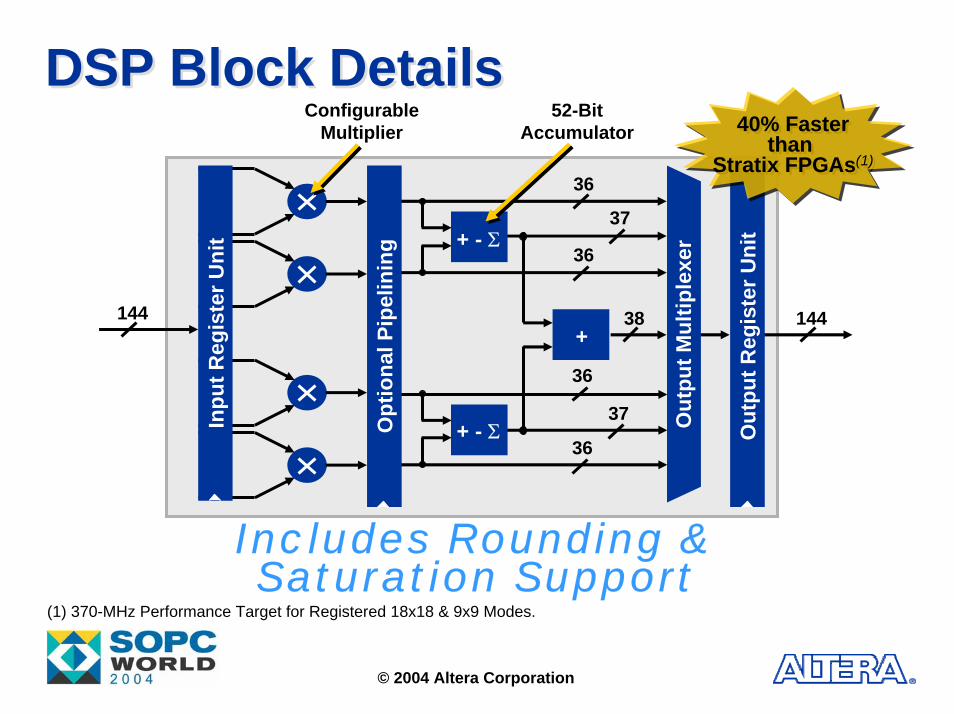
DSP Block DetailsDSP Block Details
+
Opt
iona
l Pip
elin
ing
Out
put R
egis
ter U
nit
Out
put M
ultip
lexe
r
144 144
Configurable Multiplier
52-BitAccumulator
36
36
36
36
37
37
38
+ - Σ
+ - ΣInpu
t Reg
iste
r Uni
t
40% Fasterthan
Stratix FPGAs(1)
40% Fasterthan
Stratix FPGAs(1)
Includes Rounding & Saturation Support
(1) 370-MHz Performance Target for Registered 18x18 & 9x9 Modes.
© 2004 Altera Corporation

© 2004 Altera Corporation
ALM (LE) Arithmetic ModeALM (LE) Arithmetic ModeTwo Dedicated Adders per ALM
4-LUT4-LUT
+
4-LUT4-LUT
4-LUT4-LUT
+
4-LUT4-LUT
f0
a
e0
bc
d
f1
e1
carry_in
carry_out
Reg0Reg0
Reg1Reg1
© 2004 Altera Corporation
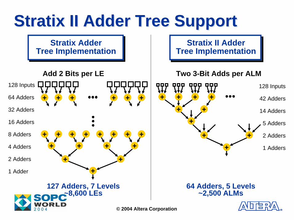
Stratix II Adder Tree SupportStratix II Adder Tree Support
127 Adders, 7 Levels~8,600 LEs
Stratix AdderTree Implementation
Stratix II AdderTree Implementation
64 Adders, 5 Levels~2,500 ALMs
Add 2 Bits per LE Two 3-Bit Adds per ALM
++ +
+ + + ++ + + + + + + +
+ + + + + +128 Inputs
42 Adders
14 Adders
5 Adders
2 Adders
1 Adders+++
+
+ + ++ ++
128 Inputs
64 Adders
32 Adders
16 Adders
8 Adders
4 Adders
2 Adders
1 Adder
© 2004 Altera Corporation© 2004 Altera Corporation
DSP Development ToolsDSP Development Tools& IP Cores& IP Cores
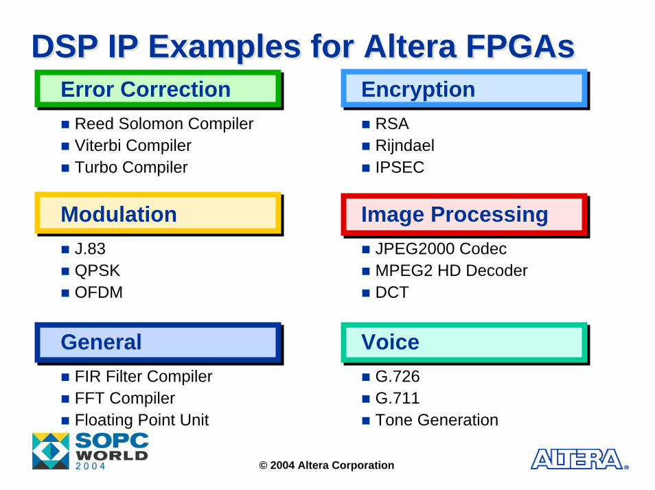
DSP IP Examples for Altera FPGAsDSP IP Examples for Altera FPGAsError Correction
Reed Solomon CompilerViterbi Compiler
EncryptionRSA Rijndael
Turbo Compiler IPSEC
ModulationJ.83QPSK
Image ProcessingJPEG2000 CodecMPEG2 HD DecoderDCTOFDM
GeneralFIR Filter CompilerFFT Compiler
VoiceG.726G.711Tone GenerationFloating Point Unit
© 2004 Altera Corporation
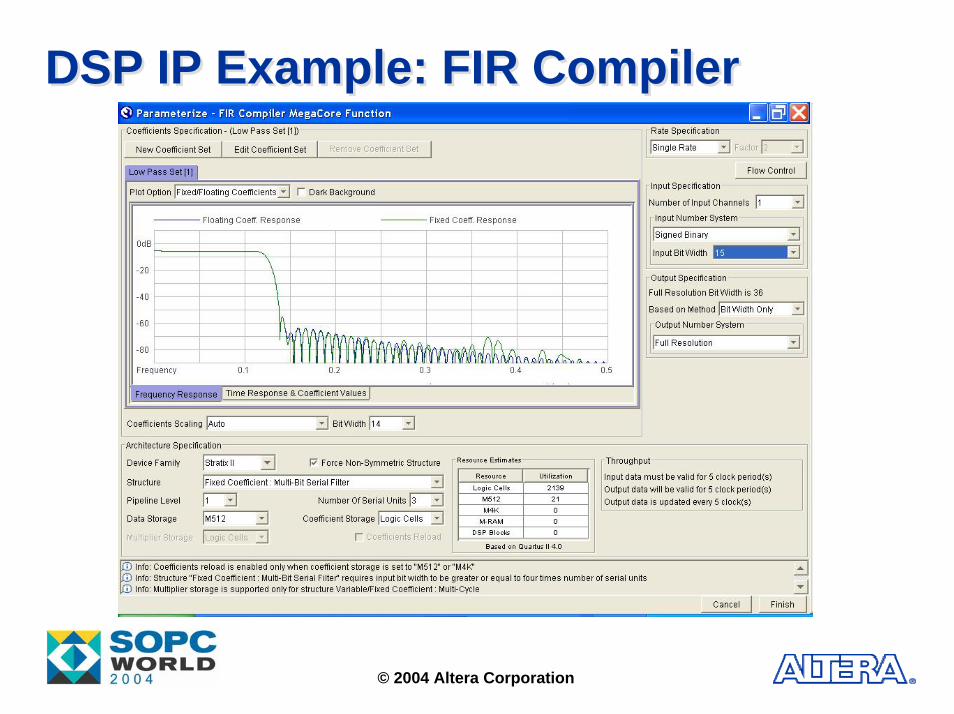
DSP IP Example: FIR CompilerDSP IP Example: FIR Compiler
© 2004 Altera Corporation
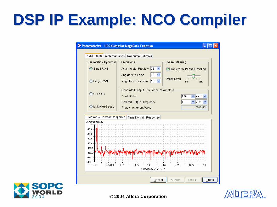
DSP IP Example: NCO CompilerDSP IP Example: NCO Compiler
© 2004 Altera Corporation
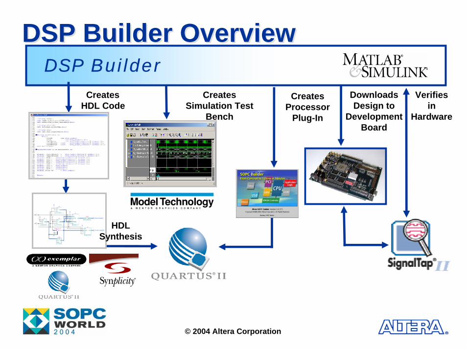
DSP BuilderDownloadsDesign to
DevelopmentBoard
CreatesSimulation Test
Bench
Verifiesin
Hardware
CreatesProcessor
Plug-In
DSP Builder OverviewDSP Builder Overview
CreatesHDL Code
HDLSynthesis
© 2004 Altera Corporation

DSP Builder Library ComponentsDSP Builder Library ComponentsArithmeticBus ManipulationComplex Signals Logical ComponentsSOPC PortsStorageMegaCore® IPRate ChangeState MachineAltera LibraryDSP Board
© 2004 Altera Corporation
© 2004 Altera Corporation
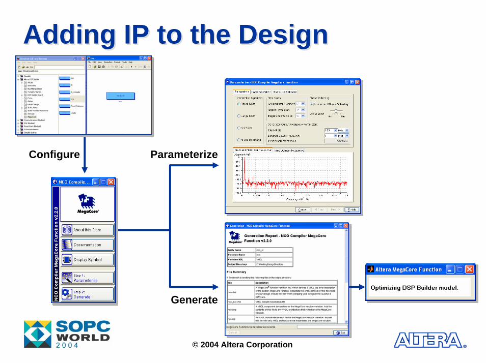
Adding IP to the DesignAdding IP to the Design
Configure Parameterize
Generate
© 2004 Altera Corporation
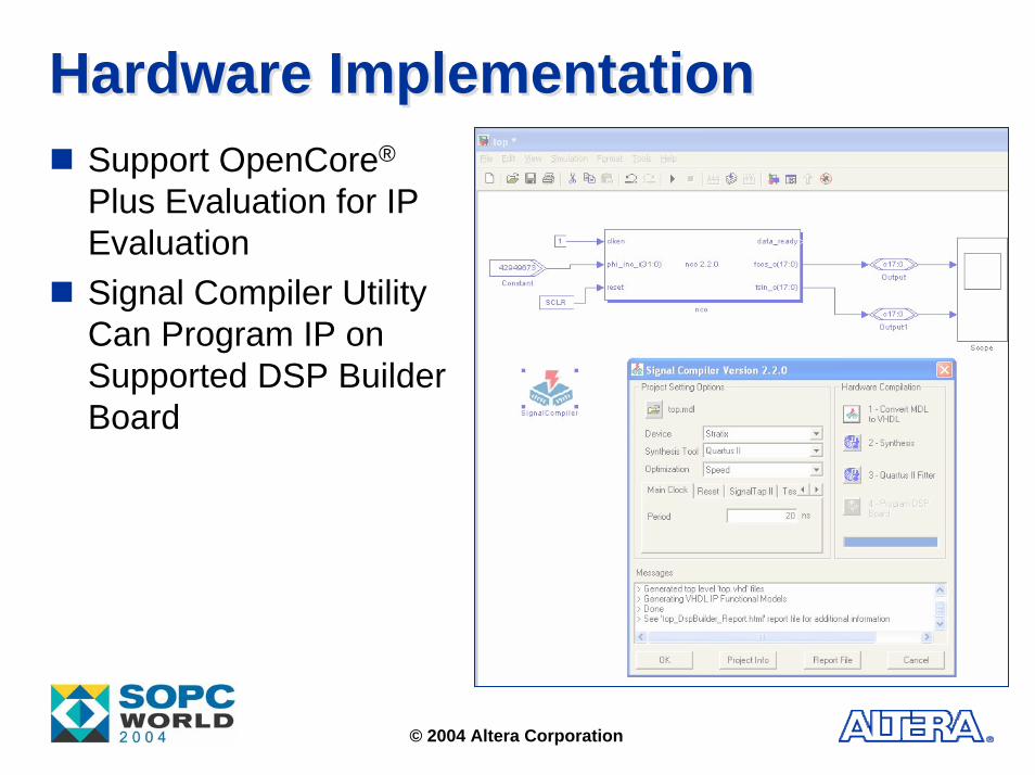
Hardware ImplementationHardware ImplementationSupport OpenCore®
Plus Evaluation for IP EvaluationSignal Compiler Utility Can Program IP on Supported DSP Builder Board

© 2004 Altera Corporation
SignalTap II Logic AnalyzerSignalTap II Logic AnalyzerInterfaces to DSP BuilderCaptures Signal Activity from Internal Device NodesDisplays Captured Data in MATLAB/Simulink
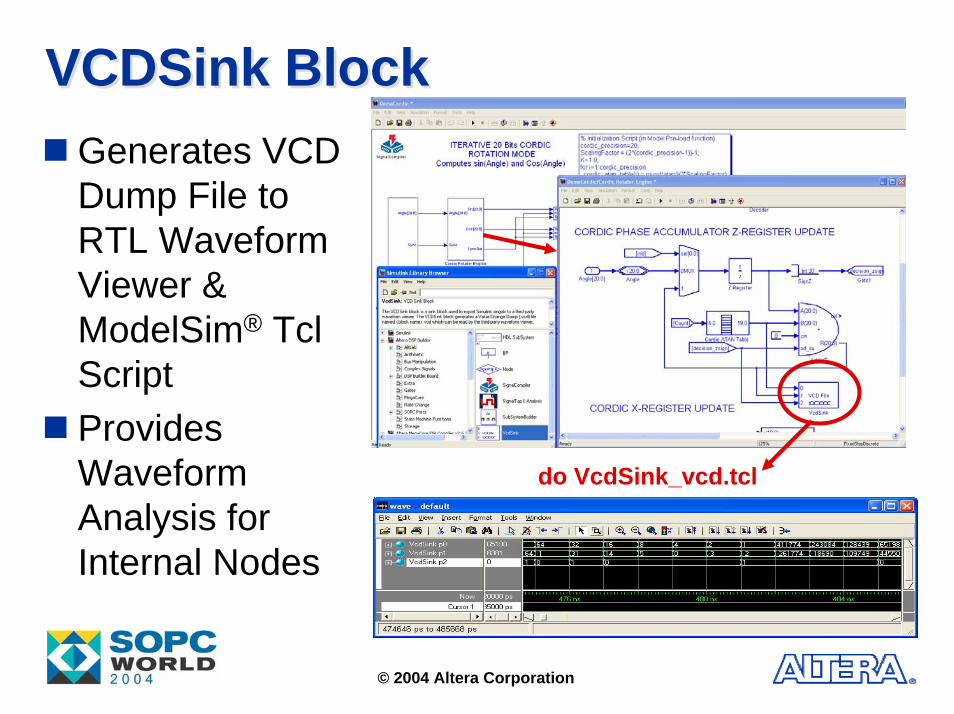
VCDSink BlockVCDSink Block
© 2004 Altera Corporation
do VcdSink_vcd.tcl
Generates VCD Dump File to RTL Waveform Viewer & ModelSim® Tcl ScriptProvides Waveform Analysis for Internal Nodes

Hardware SimulationHardware SimulationVHDL or Verilog Simulation of Simulink Design with IPSignal Compiler Generates Tcl Script to Automate MSIM SimulationUse IP Functional Model (.vho or .vo)
© 2004 Altera Corporation
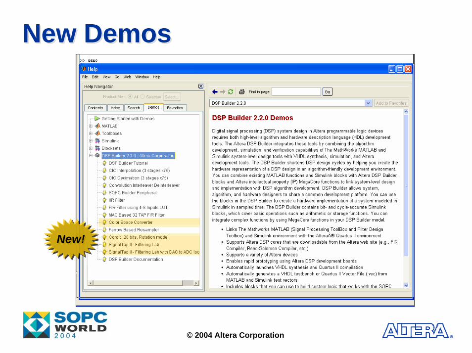
New DemosNew Demos
New!New!
© 2004 Altera Corporation
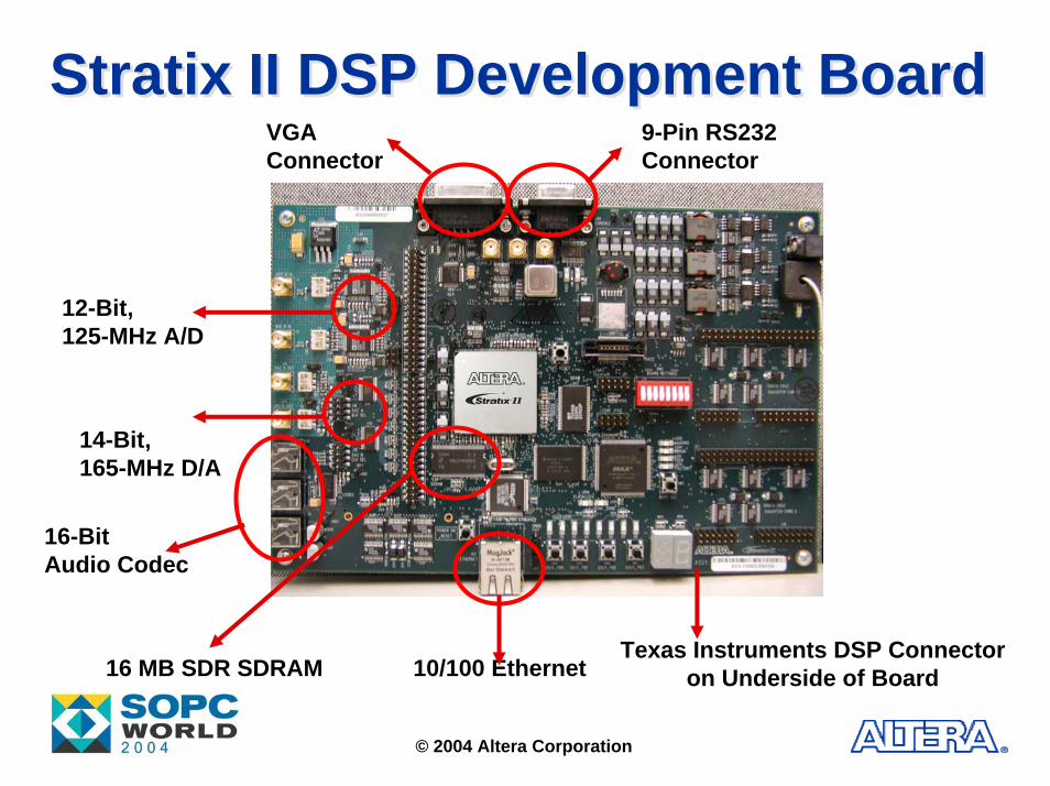
Stratix II DSP Development BoardStratix II DSP Development Board
16-BitAudio Codec
12-Bit, 125-MHz A/D
16 MB SDR SDRAM
9-Pin RS232Connector
VGAConnector
10/100 EthernetTexas Instruments DSP Connector
on Underside of Board
14-Bit, 165-MHz D/A
© 2004 Altera Corporation
© 2004 Altera Corporation
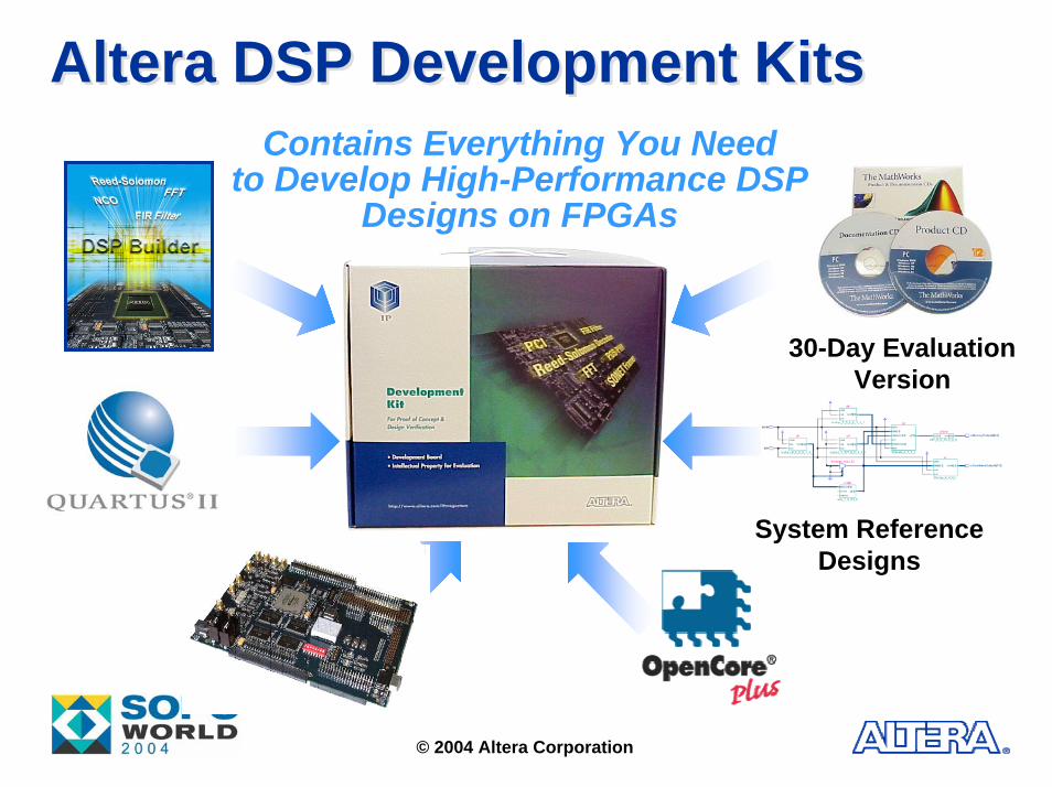
System ReferenceDesigns
Contains Everything You Needto Develop High-Performance DSP
Designs on FPGAs
Altera DSP Development Kits Altera DSP Development Kits
30-Day EvaluationVersion

NTSC,PAL & S-Video Daughter Card NTSC,PAL & S-Video Daughter Card
Available from Third PartySOPC Builder-Ready
Altera Daughter Card Connector Format
Composite In
S-Video InS-Video Out
Composite Out
VGA Out
© 2004 Altera Corporation

© 2004 Altera Corporation© 2004 Altera Corporation
FPGAs for Control & FPGAs for Control & Dataflow ProcessingDataflow Processing

Applications Driving Signal Processing Performance Requirements
Applications Driving Signal Processing Performance Requirements
Communications− Wireless Communications & High-Speed Data− Third-Generation (3G): CDMA2000, WCDMA, HSDPA,
1xEVDO/DV, etc.− WiMAX: OFDM− RF Linearization: DPD, CFR, DUC, DDC
Imaging− Security, Medical Imaging, Copiers, Studio Editing,
Broadcast High-Definition TV− H.264, WM9, JPEG2000
© 2004 Altera Corporation

Control & Dataflow Processing MixControl & Dataflow Processing MixIf, ElseCaseJumpWhile
If, ElseCaseJumpWhile
+,-,*,/,=,=>Put,get
Read,writePipe
+,-,*,/,=,=>Put,get
Read,writePipe
Con
trol
© 2004 Altera Corporation
Dataflow
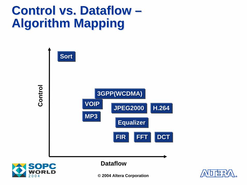
Control vs. Dataflow –Algorithm MappingControl vs. Dataflow –Algorithm Mapping
© 2004 Altera Corporation
SortSort
Con
trol
3GPP(WCDMA)3GPP(WCDMA)
EqualizerEqualizer
VOIPVOIPJPEG2000JPEG2000 H.264H.264
MP3MP3
FIRFIR FFTFFT DCTDCT
Dataflow

© 2004 Altera Corporation
Dedicated Hardware
Control vs. Dataflow – GPP vs. DSPControl vs. Dataflow – GPP vs. DSP
DigitalSignal
Processor
General-Purpose
Processor
Con
trol
Dataflow
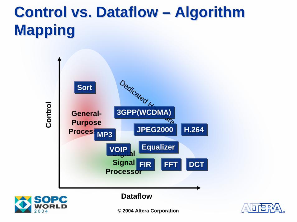
© 2004 Altera Corporation
Dedicated HardwareGeneral-Purpose
Processor
DigitalSignal
Processor
Control vs. Dataflow – Algorithm MappingControl vs. Dataflow – Algorithm Mapping
SortSort
EqualizerEqualizerVOIPVOIP
JPEG2000JPEG2000 H.264H.264
3GPP(WCDMA)3GPP(WCDMA)
FFTFFTFIRFIR DCTDCT
MP3MP3
Con
trol
Dataflow

© 2004 Altera Corporation© 2004 Altera Corporation
Hardware vs. Software Hardware vs. Software ComparisonComparisonFIR Filter DesignFIR Filter Design

© 2004 Altera Corporation
Control vs. Dataflow – Hardware vs. SoftwareControl vs. Dataflow – Hardware vs. Software
FIR Filtering Example
Con
trol
Dataflow
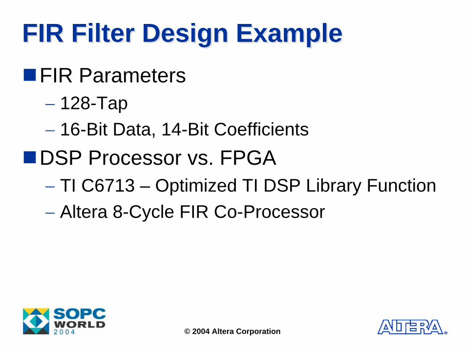
FIR Filter Design ExampleFIR Filter Design ExampleFIR Parameters− 128-Tap− 16-Bit Data, 14-Bit Coefficients
DSP Processor vs. FPGA− TI C6713 – Optimized TI DSP Library Function− Altera 8-Cycle FIR Co-Processor
© 2004 Altera Corporation
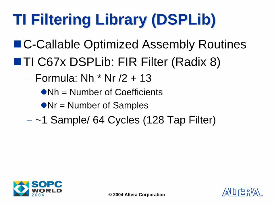
TI Filtering Library (DSPLib)TI Filtering Library (DSPLib)C-Callable Optimized Assembly RoutinesTI C67x DSPLib: FIR Filter (Radix 8)− Formula: Nh * Nr /2 + 13
Nh = Number of CoefficientsNr = Number of Samples
− ~1 Sample/ 64 Cycles (128 Tap Filter)
© 2004 Altera Corporation
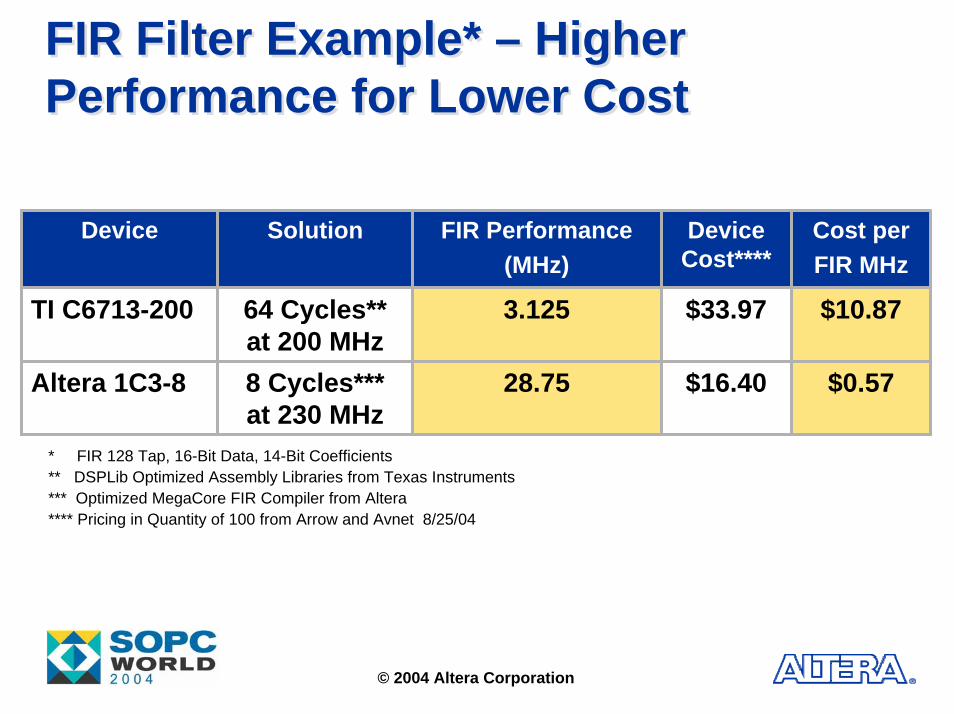
FIR Filter Example* – Higher Performance for Lower CostFIR Filter Example* – Higher Performance for Lower Cost
Device Solution FIR Performance(MHz)
Device Cost****
64 Cycles**at 200 MHz
3.125
8 Cycles***at 230 MHz
$33.97
$16.4028.75
TI C6713-200
Altera 1C3-8
Cost perFIR MHz
$10.87
$0.57
* FIR 128 Tap, 16-Bit Data, 14-Bit Coefficients** DSPLib Optimized Assembly Libraries from Texas Instruments*** Optimized MegaCore FIR Compiler from Altera**** Pricing in Quantity of 100 from Arrow and Avnet 8/25/04
* FIR 128 Tap, 16-Bit Data, 14-Bit Coefficients** DSPLib Optimized Assembly Libraries from Texas Instruments*** Optimized MegaCore FIR Compiler from Altera**** Pricing in Quantity of 100 from Arrow and Avnet 8/25/04
© 2004 Altera Corporation

© 2004 Altera Corporation© 2004 Altera Corporation
Cyclic Redundancy Code Cyclic Redundancy Code (CRC) Calculation (CRC) Calculation ExampleExample

© 2004 Altera Corporation
Control vs. Dataflow – Hardware vs. SoftwareControl vs. Dataflow – Hardware vs. Software
CRC Calculation ExampleCRC Calculation Example
General-Purpose
ProcessorCon
trol
Dataflow

CRC Algorithm – PseudocodeCRC Algorithm – Pseudocode
shiftregister = initial value (commonly 0x0000... or 0xFFFF...)while bits remain in string:
if MSB of shiftregister is set:shiftregister = (shiftregister leftshift 1) xor polynomial("leftshift" assumes big-endian architecture) else: shiftregister = shiftregister leftshift 1
xor next bit from the string into LSB of shiftregisteroutput shiftregister
Mixed Control & DataflowBit Level Manipulation of Dataflow Great for HW Acceleration
© 2004 Altera Corporation

© 2004 Altera Corporation
Accelerating SoftwareAccelerating SoftwareNios II Custom Instructions− 256 User-Defined Instructions− Fixed & Variable Cycle Operation− User Logic Import Wizard− Called as C Subroutine
Example: CRC Algorithm (64 Kbytes)
0
5,000,000
10,000,000
15,000,000
20,000,000
25,000,000
Clo
ck C
ycle
s
Software Only CustomInstruction
27 TimesFaster
27 TimesFaster
© 2004 Altera Corporation
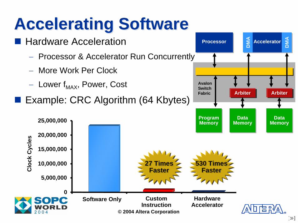
Accelerating SoftwareAccelerating SoftwareHardware Acceleration− Processor & Accelerator Run Concurrently
− More Work Per Clock
− Lower fMAX, Power, Cost
Example: CRC Algorithm (64 Kbytes)
HardwareAccelerator
ProgramMemory
Processor
DM
AD
MA Accelerator
DM
AD
MA
DataMemory
ArbiterArbiter
DataMemory
ArbiterArbiter
AvalonSwitch Fabric
0
5,000,000
10,000,000
15,000,000
20,000,000
25,000,000
Clo
ck C
ycle
s
Software Only CustomInstruction
27 TimesFaster
27 TimesFaster
530 TimesFaster
530 TimesFaster

© 2004 Altera Corporation© 2004 Altera Corporation
Utilizing Nios II for DSP Utilizing Nios II for DSP ApplicationsApplications

Nios II ArchitectureNios II Architecture
Classic Pipelined RISC Machine
− 32-Bit Instruction Set Architecture
− 32-Bit Data Path
− 32 General-Purpose Registers
− 3 Instruction Formats
− Separate Instruction & Data Caches
− On-Chip Hardware (Multiply, Shift, Rotate)
© 2004 Altera Corporation

Binary Compatibility/Flexible PerformanceBinary Compatibility/Flexible PerformanceNios II /f
FastNios II /sStandard
Nios II /eEconomy
Pipeline
Hardware Multiplier & Barrel Shifter Branch Prediction
Instruction Cache
Data Cache Configurable None None
CustomInstructions
5 Stage None6 Stage
1 Cycle
Dynamic
Configurable Configurable None
3 Cycle Emulatedin Software
Static None
Up to 256
© 2004 Altera Corporation
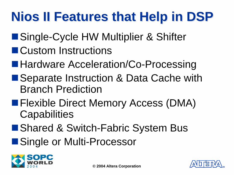
Nios II Features that Help in DSPNios II Features that Help in DSPSingle-Cycle HW Multiplier & ShifterCustom InstructionsHardware Acceleration/Co-ProcessingSeparate Instruction & Data Cache with Branch PredictionFlexible Direct Memory Access (DMA) CapabilitiesShared & Switch-Fabric System BusSingle or Multi-Processor
© 2004 Altera Corporation
Dedicated Hardware Architecture
© 2004 Altera Corporation
Perf
orm
ance
(MA
Cs/
Seco
nd)
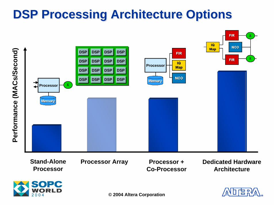
DSP Processing Architecture OptionsDSP Processing Architecture Options
DSPDSP DSPDSP DSPDSP DSPDSP
DSPDSP DSPDSP DSPDSP DSPDSP
DSPDSP DSPDSP DSPDSP DSPDSP
DSPDSP DSPDSP DSPDSP DSPDSP
Processor ArrayStand-Alone Processor
Processor
Processor + Co-Processor
Processor

© 2004 Altera Corporation© 2004 Altera Corporation
JPEG2000 ExampleJPEG2000 ExampleBarco SilexBarco Silex
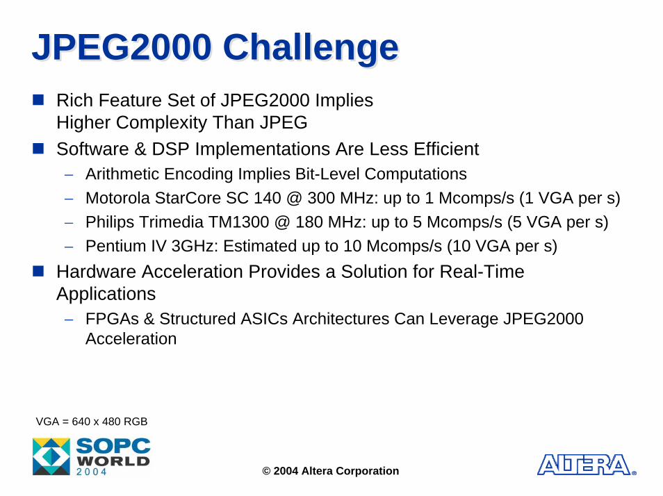
JPEG2000 ChallengeJPEG2000 ChallengeRich Feature Set of JPEG2000 Implies Higher Complexity Than JPEGSoftware & DSP Implementations Are Less Efficient− Arithmetic Encoding Implies Bit-Level Computations− Motorola StarCore SC 140 @ 300 MHz: up to 1 Mcomps/s (1 VGA per s)− Philips Trimedia TM1300 @ 180 MHz: up to 5 Mcomps/s (5 VGA per s)− Pentium IV 3GHz: Estimated up to 10 Mcomps/s (10 VGA per s)
Hardware Acceleration Provides a Solution for Real-Time Applications− FPGAs & Structured ASICs Architectures Can Leverage JPEG2000
Acceleration
VGA = 640 x 480 RGB
© 2004 Altera Corporation

JPEG2000 Accelerated by FPGAsJPEG2000 Accelerated by FPGAsCo-Processing: Unload CPU for Critical JPEG2000 Processing
Tier-2
DWT [Quant]
Entropy
Tier-2(Nios)
CPU
+
FPGA
FPGA
DWT [Quant]
Entropy
EntropyEntropy
DWTDWT [Quant][Quant]
Tier-2Tier-2
CPUSoftware
Hardware
© 2004 Altera Corporation

© 2004 Altera Corporation
General-Purpose
Processor
Control vs. DataflowControl vs. Dataflow
DataflowDataflowControlControl
Tightly/LooselyCoupled
Con
trol
Dataflow

JPEG2000 Accelerated by FPGAsJPEG2000 Accelerated by FPGAsParalleling: Boost Slowest Processing− Arithmetic Encoding (Bit-Level Algorithm)− Parallelism Configured at Synthesis Stage
Adapt the Number of Parallel Entropy Encoders to the Application Needs
DWTDWT [Quant][Quant]
EntropyEntropy
DWTDWT [Quant][Quant]
EntropyEntropy
FPGAFPGA
EntropyEntropyEntropyEntropyEntropyEntropyFPGA
© 2004 Altera Corporation
2D DWT2D
DWT QQ Tile Splitter
Tile Splitter
Entropy EncoderEntropy Encoder
Line BufferLine
BufferTile
BufferTile
Buffer
CBlock Buffer
CBlock Buffer
© 2004 Altera Corporation
Pixels
Compressed Data+ Metrics
Entropy EncoderEntropy Encoder
CBlock Buffer
CBlock Buffer
Compressed Data+ Metrics
Entropy EncoderEntropy Encoder
CBlock Buffer
CBlock Buffer
Compressed Data+ Metrics
Entropy Channels
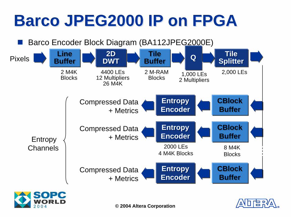
Barco JPEG2000 IP on FPGABarco JPEG2000 IP on FPGABarco Encoder Block Diagram (BA112JPEG2000E)
2 M4K Blocks
4400 LEs12 Multipliers
26 M4K
2 M-RAM Blocks 1,000 LEs
2 Multipliers2,000 LEs
2000 LEs4 M4K Blocks
8 M4K Blocks
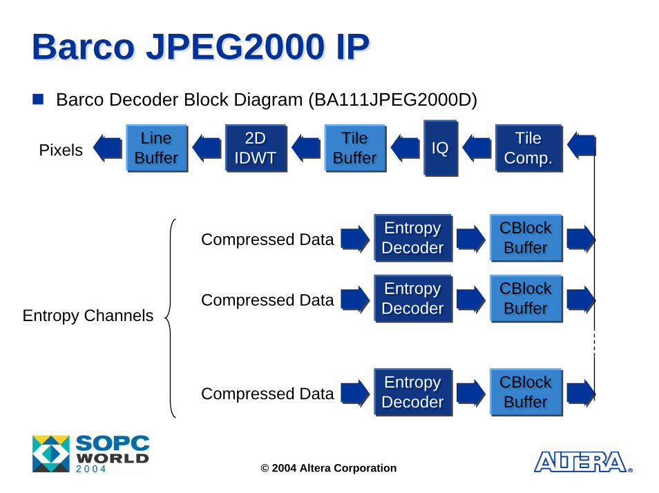
Barco JPEG2000 IPBarco JPEG2000 IPBarco Decoder Block Diagram (BA111JPEG2000D)
IQIQLine BufferLine
Buffer2D
IDWT2D
IDWTTile
BufferTile
BufferTile
Comp.Tile
Comp.
© 2004 Altera Corporation
Entropy DecoderEntropy Decoder
CBlock Buffer
CBlock Buffer
Pixels
Compressed Data
Entropy DecoderEntropy Decoder
CBlock Buffer
CBlock BufferCompressed Data
Entropy Channels
Entropy DecoderEntropy Decoder
CBlock Buffer
CBlock BufferCompressed Data

Altera Performance DataAltera Performance Data
25,000
23,400
8,400
9,400
Area (#LEs)
Decoder with 8 Channels
Encoder with 8 Channels
Decoder with 1 Channel
Encoder with 1 Channel
Encoder Configuration
156 (+2 M-RAM Tile Buffer)
57M (>> SVGA 30Hz)
124 (+2 M-RAM Tile Buffer)
72M (>> SVGA 30Hz)
44 (+2 M-RAM Tile Buffer)
8M (> CIF 30 Hz)
40 (+2 M-RAM Tile Buffer)
10M (> CIF 30 Hz)
Memory (#M4K Blocks)
Speed (comp/s)
Altera Stratix EP1S-C5, Results Given for Typical Lossy Compression
© 2004 Altera Corporation

Altera Performance: Stratix FPGAsAltera Performance: Stratix FPGAs
32/43
63/85
81/109
225/315
PACS 3M**
(ms)
8
8
6
2
# Entropy Channels
100M/74M
50M/37M
39M/29M
14M/10M
Sample Rate†/‡
EP1S60C5
EP1S40C5
EP1S25C5
EP1S20C5
Stratix Device
108/8050,000 (87%)
54/4025,000 (61%)
42/3120,500 (79%)
15/10 10,500 (58%)
VGA*
(Hz)Area (#LEs, % Usage)
* Decoding Capability Based on VGA 640x480 RGB 4:4:4 ** Decoding Capability Based on Monochrome 3-Mpixel (PACS) 2048x1536† Typical Lossy‡ Typical Lossless
© 2004 Altera Corporation
Pentium IV
Trimedia
StarCore
1M - 10M
0.5M - 5M
0.3M - 1M
1 - 10
0.5 - 5
0.3 - 1
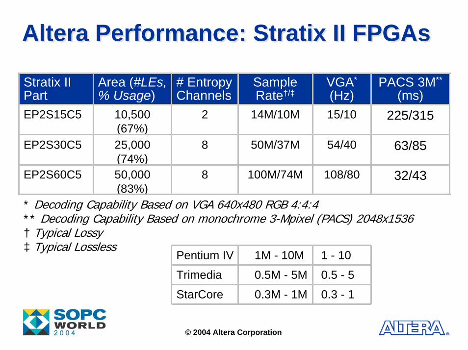
Altera Performance: Stratix II FPGAsAltera Performance: Stratix II FPGAs
32/43
63/85
225/315
PACS 3M**
(ms)
8
8
2
# Entropy Channels
100M/74M
50M/37M
14M/10M
Sample Rate†/‡
EP2S60C5
EP2S30C5
EP2S15C5
Stratix II Part
108/8050,000 (83%)
54/4025,000 (74%)
15/10 10,500 (67%)
VGA*
(Hz)Area (#LEs, % Usage)
* Decoding Capability Based on VGA 640x480 RGB 4:4:4 ** Decoding Capability Based on monochrome 3-Mpixel (PACS) 2048x1536† Typical Lossy‡ Typical Lossless
Pentium IV
Trimedia
StarCore
1M - 10M
0.5M - 5M
0.3M - 1M
1 - 10
0.5 - 5
0.3 - 1
© 2004 Altera Corporation
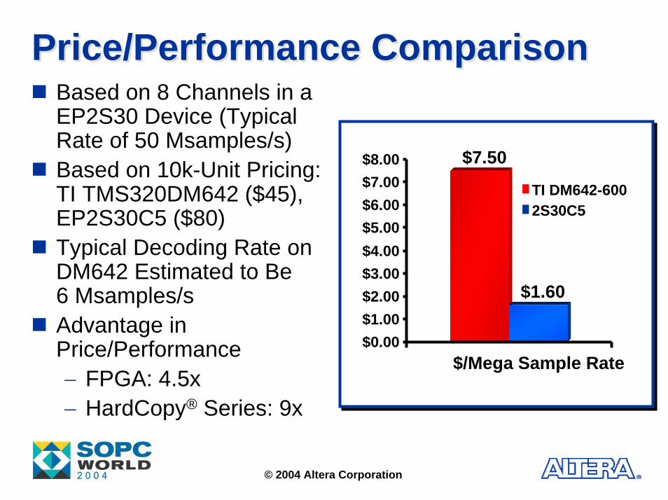
Price/Performance ComparisonPrice/Performance ComparisonBased on 8 Channels in a EP2S30 Device (Typical Rate of 50 Msamples/s)Based on 10k-Unit Pricing: TI TMS320DM642 ($45), EP2S30C5 ($80)Typical Decoding Rate on DM642 Estimated to Be 6 Msamples/sAdvantage in Price/Performance− FPGA: 4.5x− HardCopy® Series: 9x
$7.50
$1.60
$0.00$1.00$2.00$3.00$4.00$5.00$6.00$7.00$8.00
$/Mega Sample Rate
TI DM642-6002S30C5
© 2004 Altera Corporation
© 2004 Altera Corporation© 2004 Altera Corporation
Digital PreDigital Pre--Distortion Distortion ExampleExample
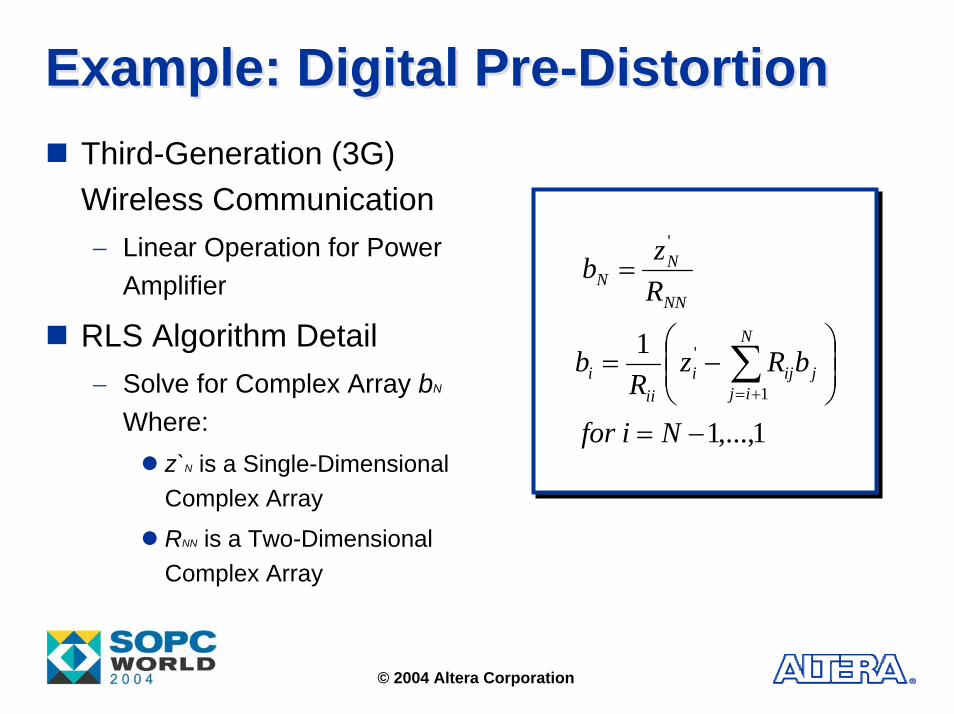
Example: Digital Pre-DistortionExample: Digital Pre-DistortionThird-Generation (3G) Wireless Communication− Linear Operation for Power
Amplifier
RLS Algorithm Detail− Solve for Complex Array bN
Where:z`N is a Single-Dimensional Complex Array
RNN is a Two-Dimensional Complex Array
1,...,1
1
1
'
'
−=
⎟⎟⎠
⎞⎜⎜⎝
⎛−=
=
∑+=
Nifor
bRzR
b
Rzb
N
ijjiji
iii
NN
NN
© 2004 Altera Corporation

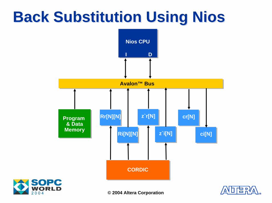
Resource Mapping for QRD-RLSResource Mapping for QRD-RLSCORDIC for QR DecompositionNios Processor for Back Substitution
DSP Blocksx(n)
LUT
CORDIC
PA
Nios
z(n) y(n)
DSP BlocksR, z’c
Y, z
© 2004 Altera Corporation
QRD-RLS
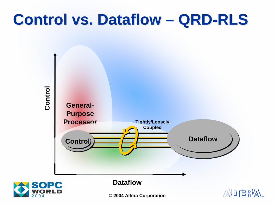
© 2004 Altera Corporation
General-Purpose
Processor
Control vs. Dataflow – QRD-RLSControl vs. Dataflow – QRD-RLSC
ontr
ol
Dataflow
DataflowDataflowControlControl
Tightly/LooselyCoupled
© 2004 Altera Corporation
Back Substitution Using NiosBack Substitution Using NiosNios CPU
I/O1Program
& DataMemory
I D
Avalon™ Bus
Rr[N][N]
Ri[N][N]
z`r[N]
z`i[N]
cr[N]
ci[N]
CORDIC

© 2004 Altera Corporation
Block DiagramBlock Diagram
X(n)
Input
Generation
X(n)
X(n)3
X(n)5
FIR Filter 3
C50 C51 C52
C’50 C’51 C’52
FIR Filter 2
C30 C31 C32
C’30 C’31 C’32
FIR Filter 1
C10 C11 C12
C’10 C’11 C’12
Program
& Data
Memory
Nios
CORDIC
Accelerator
Multiply CI
Divide CI
Sample
Buffer
Avalon Bus
D/A, AnalogueUpconverter
PA
A/D, AnalogueDownconverter
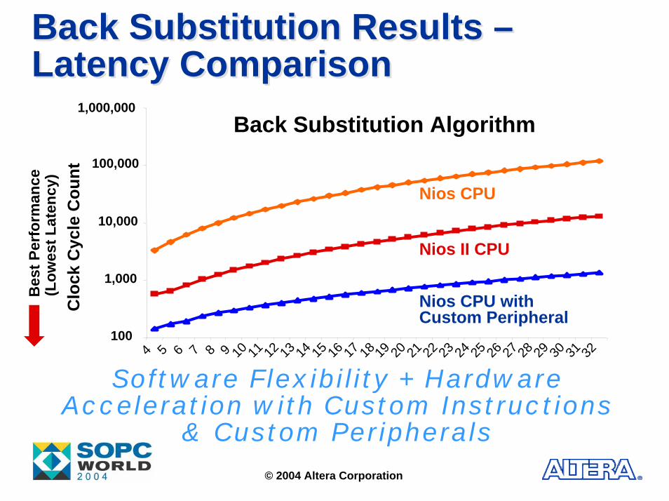
Back Substitution Results –Latency ComparisonBack Substitution Results –Latency Comparison
Bes
t Per
form
ance
(L
owes
t Lat
ency
)
Back Substitution Algorithm
100
1,000
10,000
100,000
1,000,000
4 5 6 7 8 9 10 11 12 13 14 15 16 17 18 19 20 21 22 23 24 25 26 27 28 29 30 31 32C
lock
Cyc
le C
ount
Nios CPU
Nios II CPU
Nios CPU with Custom Peripheral
© 2004 Altera Corporation
Software Flexibility + Hardware Acceleration with Custom Instructions
& Custom Peripherals
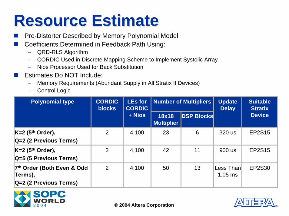
Resource EstimateResource EstimatePre-Distorter Described by Memory Polynomial ModelCoefficients Determined in Feedback Path Using:− QRD-RLS Algorithm− CORDIC Used in Discrete Mapping Scheme to Implement Systolic Array− Nios Processor Used for Back Substitution
Estimates Do NOT Include:− Memory Requirements (Abundant Supply in All Stratix II Devices)− Control Logic
Number of MultipliersPolynomial type CORDIC blocks
LEs for CORDIC + Nios 18x18
MultiplierDSP Blocks
Update Delay
K=2 (5th Order), Q=2 (2 Previous Terms)
2 4,100 23 6 320 us
K=2 (5th Order), Q=5 (5 Previous Terms)
2 4,100 42 11 900 us EP2S15
7th Order (Both Even & Odd Terms), Q=2 (2 Previous Terms)
2 4,100 50 13 Less Than 1.05 ms
EP2S30
EP2S15
Suitable Stratix Device
© 2004 Altera Corporation

Maintaining AccuracyMaintaining AccuracyFixed Point Solution− Larger Bit Widths for CORDIC & in Forward Path Intermediate Products
Floating Point Solutions− Forward Path: Floating Point Operations (multiply, add)− Feedback Path
Implement Systolic Array with Floating Point Operations—No CORDICImplement Systolic Array with Floating Point CORDIC
Hybrid Solution − Floating Point Operations
Forward Path Calculation of High Order Terms to Be Fed into Systolic Array in Feedback Path
− Fixed Point Operations CORDIC Blocks (with Floating Point Extension) in Feedback Path
Right Solution− Depends on Performance—Cost Requirements for Individual Customers
© 2004 Altera Corporation

Resource Comparison of OptionsResource Comparison of OptionsFixed Point Solution (e.g., Extending Bit Widths from 16 to 32)− CORDIC Resources Increase by ~250%− Multipliers Required Increase by up to 300%
Floating Point Operators (multiply, divide, add)− Require ~20-30% More Resources than Equivalent
Fixed Point Operators− Employ the Use of Barrel Shifters
Floating Point CORDIC vs. Fixed Point CORDIC− ~20-30% Larger− Requires Barrel Shifters− Slower Throughput as Non-Pipelined (Serial
Architecture)
© 2004 Altera Corporation
© 2004 Altera Corporation© 2004 Altera Corporation
FPGA CoFPGA Co--Processor Processor Reference DesignReference DesignTurbo Encoder for HSDPATurbo Encoder for HSDPA
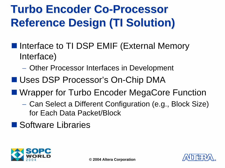
Turbo Encoder Co-Processor Reference Design (TI Solution)Turbo Encoder Co-Processor Reference Design (TI Solution)
Interface to TI DSP EMIF (External Memory Interface)− Other Processor Interfaces in Development
Uses DSP Processor’s On-Chip DMAWrapper for Turbo Encoder MegaCore Function− Can Select a Different Configuration (e.g., Block Size)
for Each Data Packet/BlockSoftware Libraries
© 2004 Altera Corporation
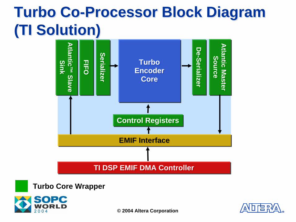
Turbo Co-Processor Block Diagram (TI Solution)Turbo Co-Processor Block Diagram (TI Solution)
Atlantic™
Slave Sink
Atlantic™
Slave Sink
Atlantic M
aster Source
Atlantic M
aster Source
TurboEncoder
Core
TurboEncoder
Core
FIFOFIFO
De-Serializer
De-Serializer
Control RegistersControl Registers
EMIF InterfaceEMIF Interface
TI DSP EMIF DMA ControllerTI DSP EMIF DMA Controller
SerializerSerializer
Turbo Core Wrapper
© 2004 Altera Corporation

Data BufferingData BufferingFIFOs in Atlantic Slave Sink Store EMIF 64-Byte Bursts While Being Serialised into CoreSlave Sink in Receive Converter Has Similar FIFOFIFOs Introduce Latency But:− Throughput Is Maintained− System Bus Not Tied Up During
Serialization/Deserialization
© 2004 Altera Corporation

Example Software EnvironmentExample Software Environment
Running on TI DSPUses EDMA Controller to Transfer Data− To & From Accelerator
Asynchronous, Streaming, Interface− Callback when Packet is Complete− Can Submit 2nd Packet Before 1st Is Done
Callbacks Occur in Order
© 2004 Altera Corporation
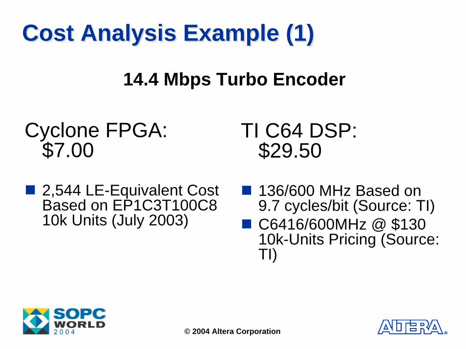
Cost Analysis Example (1)Cost Analysis Example (1)
14.4 Mbps Turbo Encoder
TI C64 DSP: $29.50
136/600 MHz Based on 9.7 cycles/bit (Source: TI) C6416/600MHz @ $130 10k-Units Pricing (Source: TI)
Cyclone FPGA: $7.00
2,544 LE-Equivalent Cost Based on EP1C3T100C8 10k Units (July 2003)
© 2004 Altera Corporation
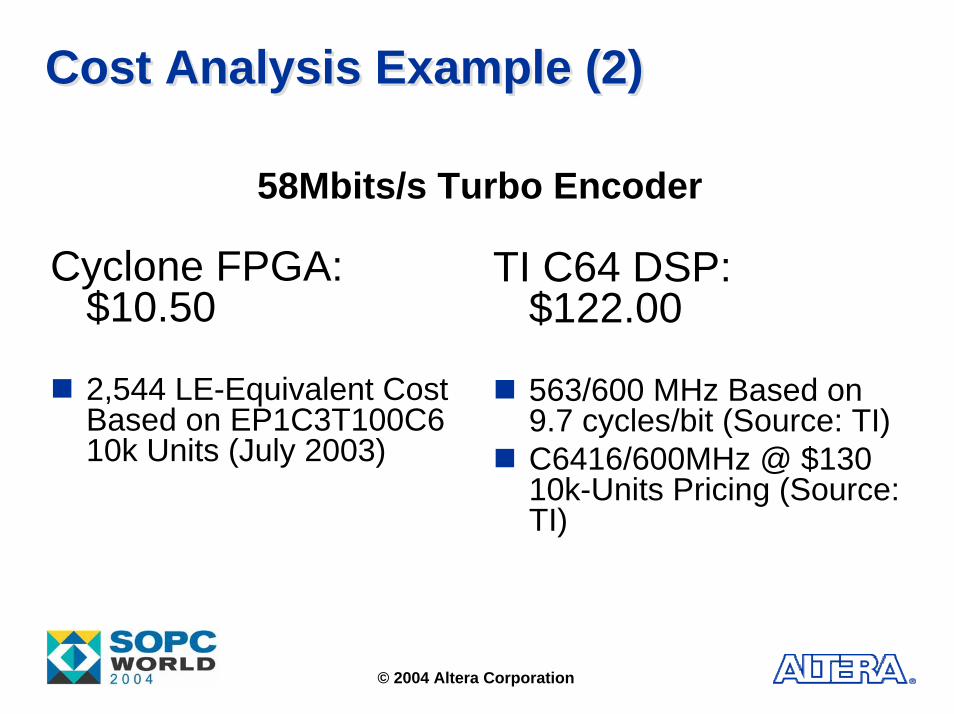
Cost Analysis Example (2)Cost Analysis Example (2)
58Mbits/s Turbo Encoder
TI C64 DSP: $122.00
563/600 MHz Based on 9.7 cycles/bit (Source: TI) C6416/600MHz @ $130 10k-Units Pricing (Source: TI)
Cyclone FPGA: $10.50
2,544 LE-Equivalent Cost Based on EP1C3T100C6 10k Units (July 2003)
© 2004 Altera Corporation

Advantages of Altera SolutionAdvantages of Altera SolutionBit Streams Make it Difficult to Exploit Digital Signal Processors’ Fixed Data Width− Most Operations Are on Bit Level (CRC, Turbo Coding,
Interleaving, Scrambling, etc.)Multiple Channels Easy to Implement− Highly Parallel Implementation Possible
Minimizes Latency (HSDPA)Minimizes Need for Temporary Storage
− Efficient Timesharing Architectures for Main Elements on PLDsPLDs Allow Full Control for Size/Speed Trade-Off for Each ComponentLow-Cost Cyclone Family Provides Cost Advantage
© 2004 Altera Corporation

© 2004 Altera Corporation© 2004 Altera Corporation
Thank You !Thank You !