mechanisms of silicon etching in fluorine- and chlorine-containing...
TRANSCRIPT

Pure & Appl. Chem., Vol. 62, No. 9, pp. 170%1720,1990. Printed in Great Britain. @ 1990 IUPAC
Mechanisms of silicon etching in fluorine- and chlorine-containing plasmas
Daniel. L. Flamm
Department of Electrical Engineering, University of California, Berkeley, CA 94720 U.S.A.
Abstract - Silicon can be etched in fluorine- and chlorine- containing plasmas in many ways. This article discusses some of the basic chemical and physical phenomena which play a role and more complicated interactions and side effects found in commercial process equipment.
INTRODUCTION
Circuit patterns are transferred to silicon by exposing surfaces of this material to the species formed in fluorine and chlorine-containing plasmas. The physics and chemistry associated with these processes have been studied for many years, and in broad form they are understood.
The elementary interactions of free halogen and halogen-containing species with silicon are discussed below, and in turn they are connected to the complex phenomena and chemical feeds which have been developed for use in semiconductor production lines.
Phenomenological mechanisms of etching In general, we may divide etching mechanisms into the four basic phenomenological categories shown in Figure 1, sputtering, chemical etching, ion-enhanced energetic mechanisms and ion-enhanced inhibitor processes (refs. 1,2).
ION h +
1. SPUTTERING
111. ION- ENHANCED ENERGETIC
VOLATILE
VOLATILE PRODUCT
11. CHEMICAL
HIBITOR
IV. ION- ENHANCED INHIBITOR
Figure 1. The four phenomenological etching mechanisms: I. sputtering, 11. chemical etching, 111. ion- enhanced energetic etching and IV. ion-enhanced inhibitor etching.
Briefly, sputter mechanisms include those in which material is mechanically ejected from a surface by the energy and momentum transferred in energetic ion bombardment. Virtually any material can be sputtered if the ion energy is high and the pressure is low enough for ejected matter to be thrown across the reactor with few collisions. Consequently, pressures on the order of a millitorr or below are required for efficient sputter etching, since the apparatus dimensions are typically some centimeters, and the mean free path of low energy neutral species is about 5/pcm, (p is the pressure in millitorr). Sputtering is unselective and generally slow.
The remaining three mechanisms, described in the following, are fundamentally different from sputter removal in at least two ways: a) chemical reactions are central to the the etching process and b) the substrate is converted into volatile, gaseous products. Hence, unlike sputter etching, the other mechanism do not depend on a long mean free path, nor is the amount of material removed sharply limited by the ion current to the surface. A third characteristic of sputtering is the geometrical facets which are produced. While a discussion is beyond the scope of this article, briefly, sputter removal is at a maximum when the surface is inclined about 40" to 60" to ion trajectories; thus sputter-etched planes tend to form along this angle to the surface.
Chemical plasma etching mechanisms are those in which the discharge creates uncharged etchant radicals which react with a surface material through conventional chemical reactions. Although the plasma also contains charged particles, they do not participate in the "chemical" etching reactions. Of course ions may still induce secondary effects such as general surface heating, or sputter "cleaning" of contaminative "native oxide" from the surface.
1709

1710 D. L. FLAMM
In contrast to the other mechanisms, Chemical etching is often, but certainly not always, isotropic or nondirectional. If the reactions take no preferred direction, material wiU be removed from sidewalls under a mask at the same rate as material is etched in a vertical direction. This omnidirectional attack causes undercutting of a mask and leaves a circular profile, as shown in Figure lb. Note, however, that chemical etching can be directional and there are chemical systems where there is preferential attack along certain crystallographic directions. Important examples are chlorine etching of GaAs, where perfectly vertical features can form, and chlorine etching of undoped crystalline silicon, which tends to expose the slow etching { 111) crystal planes (ref. 2).
The etching of silicon by free fluorine atoms is a good example of an isotropic chemical mechanism. Reaction is ordinarily rapid and fluorine atoms can survive in a gas flowing long distances from the plasma where these species are created. As a result, fluorine atom etching can be done using a "remote" or afterglow plasma reactor, where the plasma that makes the etching species is far upstream of the surface that is being etched.
Energetic ion-assisted plasma etching mechanisms remove materials that would not otherwise be gasified by plasma- generated species. Etching is made possible by the disruptive effect of ions bombarding a surface. This phenomena is sometimes referred to as the "damage" mechanism, but the term is only figurative since a variety of distinct effects can accelerate reactions and probably do- depending on the details of the plasma chemistry and the composition of the surface. Plasma etching of undoped silicon in chlorine plasmas fits neatly into this mechanistic niche (discussed below), since at ordinary temperature chlorine atoms and molecular chlorine barely attack undoped silicon at all when there is no ion bombardment.
In the fourth category, an "inhibitor" film induces anisotropy under circumstances where etching is spontaneous and the mechanism would ordinarily be purely chemical. With suitable plasma conditions, the ion flux (which is perpendicular to the surface) prevents the deposition and growth of inhibitor on horizontal surfaces, so that inhibitor selectively deposits on feature sidewalls where it prevents attack. Inhibitor films can be formed from feed additives, from the main feed component, from reaction products or even from the mask material, depending on detailed process conditions. In fluorine and chlorine etching, the perfluoroethylene-like sidewall films which stimulate anisotropy are made by adding fluorocarbons that decompose and create oligomeric, unsaturated polymer-forming species ([CF&) in the plasma.
The literature contains many terms that have been coined to describe etching mechanisms. Among the common phrases are "chemical sputtering," "reactive sputtering" and "reactive ion etching." The first two were used to describe hypothetical processes in which energy deposited by ions induces further chemical reactions between surface reaction products. I dislike these terms because they pretend to be mechanistic, and yet in reality they are vague. The term reactive ion etching sounds like a scenario in which ions consume the substrate, yet plasma ion fluxes are ordinarily far too low to do this. These three, and many similar labels, fit neatly in the "energetic ion-enhanced etching" niche. The nomenclature is especially confusing to newcomers since "sputtering" implies the purely physical removal process (above).
Having said this, still, one might consider another circumstance in which the phrase "chemical sputtering" may be appropriate and descriptive. Facet angles reminiscent of sputtering have been noted at pressures as high as lTorr, where the mean free path is far too short for material to be physically thrown off a surface without backscattering. Is there some way that sputtering can remove material despite the high pressure? The answer is a qualified yes- if mechanically ejected material collides with and reacts with these collision partners in the gas phase to form gaseous products. For example, the reaction between atomic chlorine and SiOz is thermodynamically forbidden (at moderate temperature). However, if ions sputter Si and SiO from the oxide, reactions like
Si t nC1+ SiC1, (1) SiO + nC1+ SiOClz , Sic4 + 0 (2)
can consume the ejected species in the gas phase so they will not be redeposited. The distinction, between this scheme and energetic ion-enhanced etching, is that here the ion-affected (sputtered) material is first sputtered from the substrate and the ensuing material removal rate is regulated by this (slow) sputtering. Of course such a "chemical sputtering" and energetic ion-enhanced reactions can (and probably do) take place at the same time.
Yet one more potential synergism between chemical reactions and sputtering is through the conversion of slow- sputtering surface matter into faster-sputtering products. For instance if the surface of a silicon surface were converted to chlorides by chemisorption, e.g.
Si + C1 + SiClqsurtace (3) conceivably, the chemisorbed product (SiCl.+,,,,) could be sputtered faster than Si. Here again, the etch rate would reflect a sputter process and be limited by the ion flux and (low) sputter yields. However, practical process etch rates and a large body of basic data argue that the ion-assisted etching of silicon by chlorine is mainly chemical, not physical.
Conditions and mechanism In many plasma chemistries, the mechanisms described in the first section all can and do take place to some degree. Which process is dominant is heavily influenced by plasma operating parameters such as pressure, excitation frequency, power etc. A comprehensive discussion of these effects is beyond the scope of this article and has been covered elsewhere (refs. 1,2). I shall only highlight a few pertinent trends as they pertain to parallel plate (planar) discharges without a magnetic field. However the effects are very general; while geometry, external fields etc. are important influences, the qualitative phenomena stiU apply.

Silicon etching in fluorine- and chlorine-containing plasmas 1711
As pressure is decreased below about lOOmTorr, the potential across the discharge characteristically increases, and with this there is a corresponding rise in sheath potentials. At very low pressure, the ion energy is high, reactant density is low and the mean free is long so that sputtering tends to dominate (Fig. 2). At somewhat higher pressure, the ion energy is a bit lower and neutral reactant densities are large enough to support energetic ion-assisted etching. Still higher pressures favor chemical etching and inhibitor ion-assisted directional etching.
Excitation frequency has an analogous effect, as shown in Figure 3. Ion energy tends to be moderate when the frequency is above about 3 - 5 M H z , but the potential rises steeply below about 1-3MHz. The etching rate of a substance by energetic ion-enhanced mechanisms will track these variations, as exemplified by undoped polysilicon in a C12 plasma, shown in this figure.
PHYSICAL t (SPUTTER ETCHING)
ION-ASSISTED ETCHING (DAMAGE MECHANISM)
Q
CHEMICAL PLASMA ETCHING
0.001 0.01 0.1 1.0 10 100 PRESSURE (Torr)
Fig. 2. Qualitative effect of pressure on ion energy and the etching mechanism (after ref. 2).
- 2000
-1000 * -500 >n
-200
0.1 1 .o 10 100 FREQUENCY (MHz)
Fig. 3. Frequency effects on applied FW voltage and etching of undoped silicon in a C12 Plasma (after ref. 2).
Processes leading to plasma etching can be viewed in another way. One may think of a series of steps, some which must occur serially, others in parallel, which together comprise the gasification process. A fairly general step-by-step description, etchant formation, adsorption of etchant on the substrate, chemical or ion-assisted reaction, and product desorption is adapted to describe chlorine plasma etching of silicon:
Etchant Formation e t Clz + 2C1 + e
Adsorption on Substmte
Chemical Reaction Si - nC1 + SiClx(ad,)
Ion-Assisted Reaction (ions)
Si - nC1 - SiClx(ad,)
Product Desorption siclx(ads) + siclx(gas)
(4)
(7)
Etchant must first be formed in the plasma (4) and then adsorbed on the substrate (5) . Next, the etchant combines with the substrate to form a volatile product (6, 7), in one of two ways. If spontaneous chemical reaction is fast, as in the case of high& n-doped Si reacting with atomic chlorine, process (6) may dominate. However when the chemical reactions are slow, as in the reaction of undoped Si with C1, ion bombardment may be required to drive the reaction reaction (7, energetic ion-assisted mechanism). Finally, the product formed in these reactions must be desorbed (8). In principle any one of these processes may be a step which controls the overall etching rate. In fact, process conditions may be chosen to intentionally select the rate-limiting step. For example, at low pressure and elevated temperature, doped polysilicon etching will ordinarily be limited by the concentration of etchant (4). But if the process is carried out at low temperature where the silicon chloride reaction product is less volatile, desorption (8) becomes rate-limiting, and reaction product on the sidewall can induce anisotropy (e.g. the inhibitor mechanism with reaction product as the sidewall inhibitor).
1712 D. L. FLAMM
BASIC MECHANISMS AND 'REAL PROCESS'
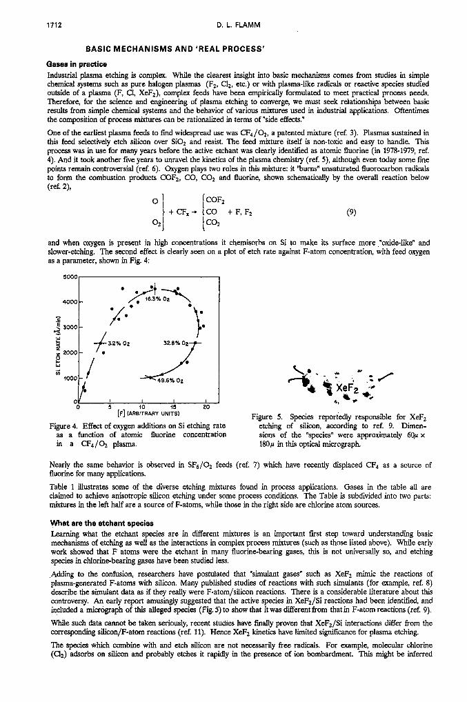
Gases in practice Industrial plasma etching is complex. While the clearest insight into basic mechanisms comes from studies in simple chemical systems such as pure halogen plasmas (F2, C12, etc.) or with plasma-like radicals or reactive species studied outside of a plasma (F, Cl, XeF2), complex feeds have been empirically formulated to meet practical process needs. Therefore, for the science and engineering of plasma etching to converge, we must seek relationships between basic results from simple chemical systems and the behavior of various mixtures used in industrial applications. Oftentimes the composition of process mixtures can be rationalized in terms of "side effects." One of the earliest plasma feeds to fmd widespread use was CF4/02, a patented mixture (ref. 3). Plasmas sustained in this feed selectively etch silicon over Si02 and resist. The feed mixture itself is non-toxic and easy to handle. This process was in use for many years before the active etchant was clearly identified as atomic fluorine (in 1978-1'379, ref. 4). And it took another five years to unravel the kinetics of the plasma chemistxy (ref. 9, although even today some fine points remain controversial (ref. 6) . Oxygen plays two roles in this mixture: it "burns" unsaturated fluorocarbon radicals to form the combustion products C0F2, CO, C02 and fluorine, shown schematically by the overall reaction below (ref. 2),
and when oxygen is present in high concentrations it chemisorbs on Si to make its surface more ,"oxide-like" and slower-etching. The second effect is clearly seen on a plot of etch rate against F-atom concentration, with feed oxygen as a parameter, shown in Fig. 4:
Figure 5. Species reportedly responsible for XeF2 etching of silicon, according to ref. 9. Dimen-
as a function of atomic fluorine concentration sions of the "species" were approximately 60p x in a CF4/02 plasma. 180p in this optical micrograph.
[F] (ARBITRARY UNITS)
Figure 4. Effect of oxygen additions on Si etching rate
Nearly the same behavior is observed in SF6/02 feeds (ref. 7) which have recently displaced CF4 as a source of fluorine for many applications. Table 1 illustrates some of the diverse etching mixtures found in process applications. Gases in the table all are claimed to achieve anisotropic silicon etching under some process conditions. The Table is subdivided into two parts: mixtures in the left half are a source of F-atoms, while those in the right side are chlorine atom sources.
What are the etchant species Learning what the etchant species are in different mixtures is an important first step toward understanding basic mechanisms of etching as well as the interactions in complex process mixtures (such as those listed above). While early work showed that F atoms were the etchant in many fluorine-bearing gases, this is not universally so, and etching species in chlorine-bearing gases have been studied less.
Adding to the confusion, researchers have postulated that "simulant gases" such as XeF2 mimic the reactions of plasma-generated F-atoms with silicon. Many published studies of reactions with such simulants (for example, ref. 8) describe the simulant data as if they really were F-atom/silicon reactions. There is a considerable literature about this controversy. An early report amusingly suggested that the active species in XeFz/Si reactions had been identified, and included a micrograph of this alleged species (Fig. 5) to show that it was different from that in F-atom reactions (ref. 9).
While such data cannot be taken seriously, recent stucbes have finally proven that XeFz/Si interactions differ from the corresponding silicon/F-atom reactions (ref. 11). Hence XeF2 kinetics have limited significance for plasma etching. The species which combine with and etch silicon are not necessarily free radicals. For example, molecular chlorine ( C l 2 ) adsorbs on silicon and probably etches it rapidly in the presence of ion bombardment. This might be inferred

Silicon etching in fluorine- and chlorine-containing plasmas
TABLE 1. Fluorine and Chlorine Bearing Gas Mixtures Reported for Anisotropic Etching
Atomic halogen formed in the gas phase
F from NF3 etching Si, med. pressure, high w
Mixture Comments NF3/Ar Shallow trench in hexode,
sF6/ f i At low pressure and
sF,/az/He
undercuts if percent NF3 high
low F concentration Trench etch; 90% He in mixture at 75mT, excess sF6 causes undercut
sF6/-3 Isotropic without -3
sF6/cFc13 Isotropic without CFC13
GFy/oz '34, qF6. Sharply limit Oz concentration in feed
Chemical/Isotropic
Mixture Comments c12 /Ar
C&/O, IkApolysilicon etched
CCI3F/Clz Trench etching using to gate oxide
TEOS Oxide Mask
Adsorbed feed Molecules
CC13F/O2
CHCI,/N2
Cl2/SiC&
Polysilicon etch with oxide mask, polymer sidewall can form Trenching, reportedly no Si etch without N2, suggest C removed as CN. Trench etching in a "triode"
F from NF3 on Si02, low w
CI2 in Al etching
Ion bombardment, anisotropic
Can be anisotropic w/inhibitor
BCl3/Clz
CC&/02 Crystallographic effects noted,
CC12F2/H2 Taper etching, H2
Trench etching at 15 mT in hexode with oxide mask
anisotropic Si profile
causes an "overcut" profile
CI2 on doped Si
Cl2 etching Si, low pressure
TABLE 2. What are the etchant species?
POSSIBILITIES I Candidate EXAMPLE I COMMENTS I I
Chemical, Isotropic
Ion bombardment, anisotropic
Adsorbed product layer CxFy in unsaturated feed SO2 etching
Ion bombardment, anisotropic, product layer may be complex
Fragment radical
1713
C&/H, etching GaAs Ion bombardment, anisotropic
I Clt for undoped Si I Ion bombardment, anisotropic
from the early work of Smith (ref. 12) in which the reactivity of products effusing from a chlorine discharge (in all likelihood, mostly Cl,) increased with the energy of a coincident argon ion beam increased (Fig. 6).
Note that aluminum etching in this system (also shown in the figure) is rapid and unaffected by ion bombardment (Cl, is known to attack aluminum about as fast as Cl).
Besides atoms and adsorbed molecules, some more complex species tentatively identified as etchants in certain systems, are shown in Table 2. It is likely that adsorbed fluorocarbon layers may slowly attack silicon under some conditions (with ion bombardment, ref. 2) and fragment radicals from SF6 discharges probably adsorb to become an anisotropic etchant for silicon at very low pressures and/or temperature (ref. 13).
ION-BOMBARDMENT ENERGY ( e V ) no ion bombordmcnt 0 4.200 + 400
I I I I I I
- Si IN CI. Al IN CI, ----*
I I I I I I
-200 0 + 200 t 400 0 '
Figure 6. Product signal from silicon and aluminum exposed to the effluents of a CI, discharge and argon ions as a function of ion energy (after ref. 12).
BEAM DC BIAS ( V )
1714 D. L. FLAMM
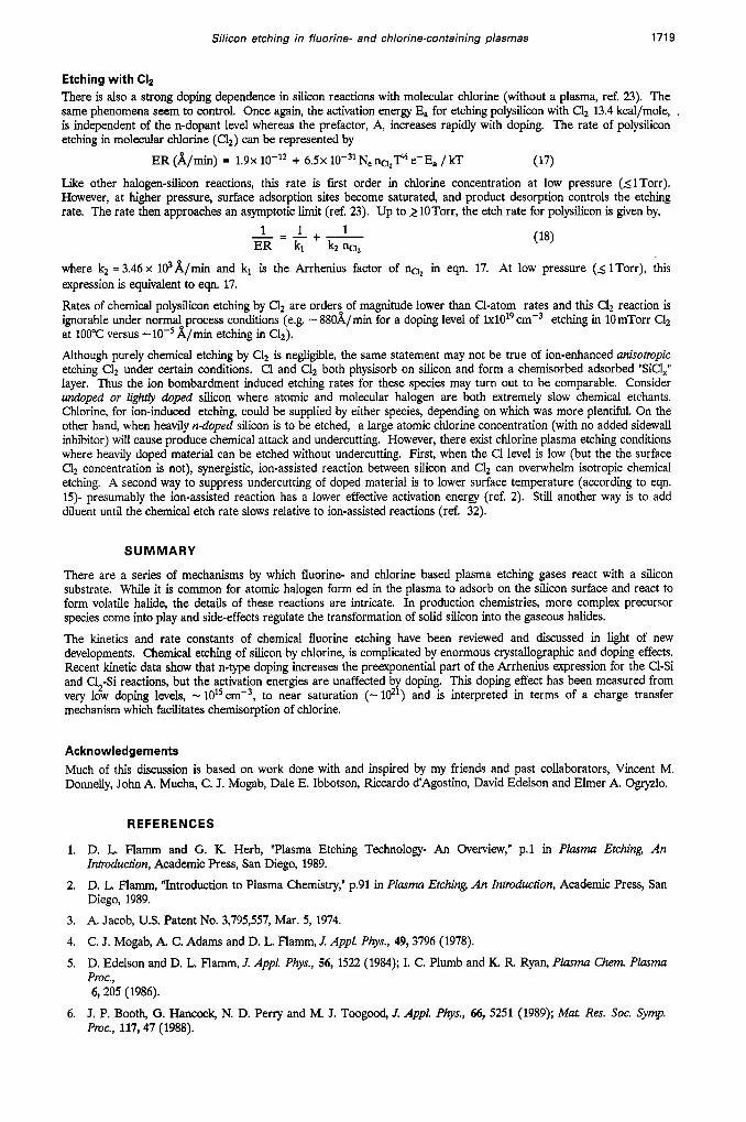
Side effects in etching If the reactions between etchant and pure substrate are the main event in etching, then other phenomena that are not a direct part of these reactions might be termed "side effects." The complexity of feed gases and etching systems may be understood in terms of these secondary phenomena. Of course some "side effects" are nearly unavoidable in all etching processes and they can either be beneficial or harmful. Such effects arise from the chemistry of feed additives, others stem from variability in substrate composition, and still other things are attributable to reactor chamber design. A few effects are listed in Table 3, along with an example of each and their influence on etch rates, sidewall passivation (in inhibitor anisotropic etching), and profiles.
TABLE 3. Examples of some side-effects in etching processes.
FACTOR EXAMPLE EFFECT ON Etching Sidewall Profile
Surface Oxidation Cl2 / 0 2 Etch retardation Passivation
Heating Ions, B field Acceleration Varies ~~~
/c,,,,-ition Cu (from Al) Catalytic etch, Some undercut or inhibition
I Sputter Redeposition "Grass"? Passivation Taper I [Product Transport S i F , + 0 2 Accelerates? Passivation Taper? I
Surface Migration qFy/C12 Varies I I Polymerization sF,5 / CHC13 SlOWS Passivation Anisotropy I
Moderate amounts of oxygen increase the concentration of F formed from fluorocarbon feeds (see above), while larger O2 additions adsorb on Si surfaces and form an oxidelike layer that retards etching (ref. 2). When small amounts of O2 are added to chlorine discharges in silicon etching, selectivity over Si02 is enhanced (ref. 14, presumably by restoring oxygen to Si02 surfaces from which 0 is sputtered away, although and redeposition of oxide formed from the silicon chloride etch product is a candidate mechanism as well). Low levels of oxygen in C12 discharges may also passivate silicon feature sidewalls under some circumstances (by forming an Si02 inhibitor layer).
Surface heating is an important physical side effect; most etch rates increase with temperature, but temperature decreases selectivity (ref. 2). A rise in wafer temperature may stem from many factors, including energy deposited by ion bombardment, or localized plasma power transfer near a wafer surface (which can be caused by some magnetic field configurations).
Contamination, another side-effect, is of great concern. Contamination comes in many forms. Although the use of "ultraclean" high vacuum system hardware may exclude ambient contaminants, etching reaction products or materials on the wafer can be harmful when transported by chemical and physical processes in the plasma.
The source of contaminant and degree of susceptibility is often surprising. For example, recently it was shown that minute traces of copper, even monolayer coverage, can accelerate silicon etching by molecular fluorine or chlorine (ref. 15). Since copper is a common ingredient in aluminum metallization, sputtering of this conductor can affect silicon etch rates.
Sputtered material and unwanted oxidation can passivate surfaces and inhibit etching. Partial oxidation and sputter contamination was a common problem in early chlorine etching when there were no vacuum "load locks." Small amounts of moisture and sputtered contamination produced microscopic "masks" scattered over the substrate. If the substrate was then etched anisotropically, these micromasked areas were shielded from etchant species, leaving an array of random raised areas which resembled "grass."
Yet another kind of contamination originates from carbon-bearing species. The source of carbon can be a photoresist mask or a carbon bearing additive in the feed gas. Surface carbon in a chlorine discharge increases erosion of Si02 under ion bombardment, and thus reduces selectivity.
Despite the lower selectivity over silicon oxide, carbon bearing additives are commonly used to form inhibitor films which induce anisotropy. Data in Fig. 7 show how CFC13 prevents undercutting in an SF6 plasma. Etching is only anisotropic when there is enough Freon to maintain the sidewall fim as etching deepens the features. In the same way, heavily doped polysilicon is etched rapidly (and isotropically) by chemical reaction in chlorine plasmas, but here again a sidewall &-forming additive such as QF6, can be used to achieve anisotropy.

Silicon etching in fluorine- and chlorine-containing plasmas 1715
r Fig. 7. Effect of an inhibitor forming feed additive on linewidth in a fluorine atom etching plasma. Sidewall films formed from unsaturated decomposition products of CFC13 can suppress undercutting by preventing chemical reaction between the sidewalls and F-atoms (after ref. 16).
/ PURE SF* I
% OVERETCH
SILICON ETCHING BY ATOMIC FLUORINE
When clean silicon is exposed to atomic fluorine, it quickly acquires a fluorinated "crust," that extends about 5 monolayers into the bulk. Evidence suggests that that F atoms penetrate the top of this layer, as shown in Figure 8, and attack subsurface bonds Si-Si bonds, eventually releasing silicon in the form of two gaseous desorption products- a free radical, SiF2, and the stable product SiF4 (refs. 2, 17).
I F
Fig. 8. Mechanism of silicon etching by fluorine (after ref. 2). Simplified depiction of a two-channel concerted reaction between F- atoms and the fluorinated layer. Reaction results in the formation of gaseous SiF2 (Ia) and bound fluorosilicon radicals (Ib) that are fluorinated further to form higher SiFx
F\ / F products. Kinetics indicate that (Ia) and (Ib) -----_------ F F S i F are branches of a single, rate-limiting
\ / I / reaction that may involved a common,
/ \
E _ _ _ _ E -----, F si
/ \ 7 \si /
h / \ (1 1
Si vibrationally-excited intermediate.
These two product channels show precisely the same activation energy, probably because they come from a common activated state that dissociates into fixed proportions of SiFz and the stable groups in the surface layer. The radical species in the fluorosilicon crust then combine with more fluorine to form SiF4. This branched reaction can be followed visually, since the SiF2 radicals which are created react with F and Fz to form an excited state of SiF3 that chemilumineses with a broad peak around 500nm:
F + F-Si- -, SiF2
SiF2 + F(F2) + SiF;( t F )
~3; + SiF3 + hvcontinuurn
(10)
(11) (12)

1716 D. L. FLAMM
These reaction kinetcs are estab2hed by three facts (refs. 17, 11, 18, 19): 1) it is proven that the chemiluminescense originates from SiF3, 2) the SiF2 concentration and Si etching show the identical activation energy, and 3) the etch rate and luminescent intensity follow a rate law,
where the first term in the numerator arises from the reaction of SiF2 with atomic fluorine and the second term corresponds to the reaction with molecular fluorine, as predicted by eqns. 11. m4 and @s are the fractional yields of SiF; relative to all products which arise from the reaction of SiFz with F and F2, respectively. Studies show that most silicon leaves the surface as the product SiF4, while SiF2 amounts to only 5 to 30 percent of the nascent product. The etch rates for fluorine atom etching of Si and Si02 are given by the Arrhenius expression,
Etch Rate(A/min) = AnFT1f2e-'A/RT (14) with parameters in Table 4:
TABLE 4. Preexponential factors (A) and activation energies EA for Si and Si02 Arrhenius expressions.
EA (kcal/rnole) (298K, nF = 3x 10'5cm-3)
2.86 x 10⁻¹²
3.76 55
These parameters correspond to a room temperature selectivity for F-atom etching of Si over S O 2 of about 40:l. Note that it is the surface temperature which counts: selectivity will fall if the plasma heats the silicon surface, no matter what the bulk temperature is. Temperature is an essential process variable.
Etching with analogs and simulants As mentioned, it has often been suggested that silicon etching by F2, XeF2 and other "plasmaless etchants" goes by the same mechanism as F-atom etching. But this hypothesis is disproven by data which shows that the kinetics and product distribution in XeF2 etching are quite different (refs. l O , l l ) , and that molecular fluorine etching (F2) etching has distinct kinetics (ref. 20), with a much thinner fluorinated layer (ref. 21) during the etch process (approximately a monolayer).
Fig. 9. Arrhenius plot for the reaction for ClF3 with silicon at 4.7 Torr (from ref. 2).
i / ~ x 103, K-'
Curiously, the characteristics of silicon etching by XeF2 are more like gaseous etching with halogen fluorides than plasma etching in atomic fluorine. The halogen fluorides (ClF3, BrF3, IFs, etc. gasify silicon rapidly with well over 1OO:l selectivity against SiOz (?@ally at rates of microns per minute), and these reactions require no plasma (ref. 22). In XeF2 and interhalogen e t c h g near and below room temperature, the rate can increases as substrate temperature is reduced. That is, these gases show an apparent negative activation energy. This characteristic is illustrated by the reaction of ClFs with silicon shown in Fig. 9 (contrast the linear Arrhenius relation with atomic F, eqn. 14), and has

Silicon etching in fluorine- and chlorine-containing plasmas 1717
4
been explained by a mechanism involving physisorbed precursors (ref. 22). At reduced temperature, increasing surface etchant concentration more than compensates for the Arrhenius law decrease in reaction between etchant and sublayer.
c ‘7 100
t! ’I
SILICON ETCHING BY ATOMIC CHLORINE
Although chlorine and fluorine atom reactions with silicon both show first order kinetics and an Arrhenius behavior, (eqn. 14) the chlorine atom etching reactions are different in character from fluorine etching. Chemical etching by fluorine is isotropic, chlorine etching is strongly crystallographic as a rule (rather than isotropic) and the free carrier concentration in silicon has an enormous effect on chlorine etching rates and profies (refs. 23,24). In fact, in the absence of ion bombardment, chlorine does not etch SiOz or undoped silicon at room temperature (reaction of chlorine with Si02 is thermodynamically unfavorable).
To some degree chemical reactions between all of the halogens and silicon seem to be influenced by electrically active impurities in the lattice (“dopants”). There is some evidence that p-type doping slows silicon etching by F-atoms and that n-type dopanting m enhance this etching by roughly a factor of 2 (refs. 23-26), but the effect is small compared to the overwhelming influence of doping on chlorine atom etching rates, shown in Fig. 10.
PP- P-doped PoiySi 0--- Pdoped Si(100) a--- Sb.As-doped Si(l11)
I I I I I I
1015 1018 1017 io18 iolQ 1020 i c
Figure 10. Effect of n-type dopant concentration and crystallographic orientation on the C1 atom etching reaction with silicon at 400°K. The vertical axis gives the etch rate per d t o r r of free C1-atoms (after ref. 24).
Dopant Concentration, ~ r n - ~
Fig. 10 also shows the pronounced the influence of crystallography on the etching of light to moderately doped silicon. Long before the rates were known, researchers saw that lightly p-doped doped silicon (10’’ carriers/cm3) features were strongly faceted by chlorine etching. There were reports of a 30:l etch rate ratio between the (100) and (111) planes in moderately n-doped material, whereas no directionality was observed in the etching of heavily doped silicon (ref. 27).
81
P Fig. 11. Simplitied mechanism for the doping effect (ref. 28).
The high etch rate of nt silicon compared to undoped or p-type silicon in Cl-source plasmas has been associated with charge transfer (refs. 23,24,29,26). Activated n-type carriers raise the Fermi level with respect to the conduction and valence bands, so that electrons are more easily transferred from the silicon surface to chemisorbed C1. On undoped c 111> silicon, the distance between Si atoms is close, and in principle, a monolayer of covalently bonded C1 atoms will completely block more chlorine from reaching the silicon (refs. 28,30). Since there is a steric barrier to further

1718 D. L. FLAMM
Polysilicon
<loo>
<111>
chemisorption and chlorine penetrating into the lattice, the reaction rate is very low. N-type doping facilitates electron transfer to the the absorbed chlorine and thus stimulates formation of a more ionic surface bond, (Sld' - Cl'-. The change in bonding geometry opens up additional chemisorption sites and makes it easier for C1 to penetrate into the substrate lattice (ref 24,28). The basic idea is illustrated in Fig. 11.
"Real" surfaces are stepped and highly irregular with many kinds of of imperfections. It is also doubtful that adsorbed chlorine truly forms a uniform monolayer. Nevertheless, the Fig. 11 represents a simplified concept which predicts the observed trends.
Since steric hindrance will impede chemisorption most severly on a close-packed <111> surface (ref. 30,28), undoped material with this orientation should show the lowest etch rate and the strongest doping effect. This is in accord the data (Fig. 10). In kinetic theory, the preexponential part of the reaction rate ("A" factor, eqn. 14) is proportional to the number of active sites. According to the charge transfer model, an increase in the number of adsorption sites is the dominant effect of doping. Thus if the same reaction channel is rate determining at all doping levels, the activation energy should be nearly constant. Recent results are in agreement with these predictions. The temperature and dopant dependence of the C1-silicon reaction is fit by a generalized form of the Arrhenius expression,
4 . 0 4 ~ lo-'* 0.390 4.70 (t 0 . 2 )
1 . 0 7 ~ 0.287 4.25 ( f 0.55)
1 . 6 3 ~ 10-31 1.03 4.14 (t0.37)
E -- ER (A/-) = v N,Y ncl T I / ~ e kT A/-
L 8 1.2x10²Q
-
0
where N, is the n-type dopant concentration, and the doping effect is contained in the preexponential factor, A = v N,Y an empirical power law (refs. 24,30,31). Parameters are given in Table 5, below:
4
TABLE 5. Rate Parameters for C1-Atom Etching of Doped Silicon (after ref. 24).
-1 t g 10
I Crystallographic I V 8, m3(1 w)
kcall mole molec.('+Y) min K1/2 Orientation
Fig. 12 shows the Arrhenius behavior for polysilicon data, as a function of doping level.
0.0015 0.0020 ~ 0.0025 0.0030 0.0035
1 I T , 'K-'
Fig. 12. Arrhenius plot of chemical polysilicon etching by chlorine atoms as a function of n-type dopant concentration (after ref. 24).
According to these concepts, silicon orientations with more "open" crystallographic orientations should etch faster, which agrees with the data. Finally, as the number of surface sites grows with doping, an increase in the concentration of adsorbed chlorine might be expected. There is some indirect experimental evidence for this too (ref. 21,28).
Silicon etching in fluorine- and chlorine-containing plasmas 1719
Etching with Clz There is also a strong doping dependence in silicon reactions with molecular chlorine (without a plasma, ref. 23). The same phenomena seem to control. Once again, the activation energy E, for etching polysilicon with C12 13.4 kcal/mole, . is independent of the n-dopant level whereas the prefactor, A, increases rapidly with doping. The rate of polysilicon etching in molecular chlorine ( a 2 ) can be represented by
ER (A/min) = 1 . 9 ~ t 6 . 5 ~ N, na,TH e-E, / kT ( 17) Like other halogen-silicon reactions, this rate is fist order in chlorine concentration at low pressure (51Torr). However, at higher pressure, surface adsorption sites become saturated, and product desorption controls the etching rate. The rate then approaches an asymptotic limit (ref. 23). Up to ZlOTorr, the etch rate for polysilicon is given by,
where k2 = 3.46 x ldW/min and kl is the Arrhenius factor of na2 in eqn. 17. At low pressure (s lTorr), this expression is equivalent to eqn. 17.
Rates of chemical polysilicon etching by C12 are orders of magnitude lower than C1-atom rates and this C12 reaction is ignorable under normal process conditions (e.g. - 880A/min for a doping level of l ~ l O ' ~ c m - ~ etchhg in 10mTorr C12 at 100°C versus -lo-' @min etching in C12).
Although purely chemical etching by C12 is negligible, the same statement may not be true of ion-enhanced anisotropic etching C12 under certain conditions. C1 and Cl2 both physisorb on silicon and form a chemisorbed adsorbed SiClX" layer. Thus the ion bombardment induced etching rates for these species may turn out to be comparable. Consider d o p e d or light& doped silicon where atomic and molecular halogen are both extremely slow chemical etchants. Chlorine, for ion-induced etching, could be supplied by either species, depending on which was more plentiful. On the other hand, when heavily ndoped silicon is to be etched, a large atomic chlorine concentration (with no added sidewall inhibitor) will cause produce chemical attack and undercutting. However, there exist chlorine plasma etching conditions where heavily doped material can be etched without undercutting. First, when the C1 level is low (but the the surface C12 concentration is not), synergistic, ion-assisted reaction between silicon and C12 can overwhelm isotropic chemical etching. A second way to suppress undercutting of doped material is to lower surface temperature (according to eqn. 15)- presumably the ion-assisted reaction has a lower effective activation energy (ref. 2). Still another way is to add diluent until the chemical etch rate slows relative to ion-assisted reactions (ref. 32).
SUMMARY
There are a series of mechanisms by which fluorine- and chlorine based plasma etching gases react with a silicon substrate. While it is common for atomic halogen form ed in the plasma to adsorb on the silicon surface and react to form volatile halide, the details of these reactions are intricate. In production chemistries, more complex precursor species come into play and side-effects regulate the transformation of solid silicon into the gaseous halides.
The kinetics and rate constants of chemical fluorine etching have been reviewed and discussed in light of new developments. Chemical etching of silicon by chlorine, is complicated by enormous crystallographic and doping effects. Recent kinetic data show that n-type doping increases the preexponential part of the Arrhenius expression for the C1-Si and C1,-Si reactions, but the activation energies are unaffected by doping. This doping effect has been measured from very low doping levels, - 10'' ~ m - ~ , to near saturation (- 1@*) and is interpreted in terms of a charge transfer mechanism which facilitates chemisorption of chlorine.
Acknowledgements Much of this discussion is based on work done with and inspired by my friends and past collaborators, Vincent M. Donnelly, John A. Mucha, C. J. Mogab, Dale E. Ibbotson, Riccardo d'Agostino, David Edelson and Elmer A. Ogryislo.
1.
2.
3.
4.
5.
6.
REFERENCES
D. L. Flamm and G. K Herb, "Plasma Etching Technology- An Overview," p.1 in Plasm Etching, An Introduction, Academic Press, San Diego, 1989.
D. L. Flamm, "Introduction to Plasma Chemistry," p.91 in Plasm Etching, An Introduction, Academic Press, San Diego, 1989.
A. Jacob, U.S. Patent No. 3,795,557, Mar. 5, 1974.
C. J. Mogab, A. C. Adams and D. L. Flamm, J. AppL Phys., 49,3796 (1978).
D. Edelson and D. L. Flamm, J. Appl. Phys., 56, 1522 (1984); I. C. Plumb and K R. Ryan, Plasm Chem Plasma Proc., 6,205 (1986).
J. P. Booth, G. Hancock, N. D. Perry and M. J. Toogood, J . AppZ. Phys., 66, 5251 (1989); Mat. Res. SOC. Symp. Proc., 117,47 (1988).

1720 D. L. FLAMM
7.
8.
9.
10.
11.
12.
13.
14
15.
16.
17.
18.
19.
20.
21.
22.
23. 24.
25.
26.
27.
28.
29.
30
31.
32.
R. d'Agostino and D. L Flamm, J. AppL Phys., 52, 162 (1981).
J. A. Yarmoff and F. R. McFeely, Phys. Rev. B., 38,3057 (1988).
Anonymous, Solid State Technology, 4,321 (1983).
a) D. E. Ibbotson, D. L Flamm, J. A. Mucha and V. M. Donnelly. AppL Phys. Lett., 44, 1129 (1984); D. L. Flamm, D. E. Ibbotson, J. A. Mucha and V. M. Donnelly, Solid State Technology, 4, 117(April, 1983).
M. J. Mitchell, M. Suto, L. C. Lee and T. J. Chuang, J. Vm. Sci TechnoL, B5, 1444 (1987).
D. L. Smith and R H. Bruce, J. Elecfmchem SOC., 129,2045 (1982).
K Nhomiya, K Suzuki, S . Nishimatsu and 0. Okada, J. AppL Phys., 62, 1459 (1987): S. TacG K Tsujimoto and S . Okudaira, Appl. Phys. Lett., 52,616, 1988; J. Hopwoon, K K Reinhard, J. Asmussen, J. Vm. Sci Technol., B6, 1896 (1988).
J. M. Cook, D. E. Ibbotson and D. L. Flamm, J. Vm. Sci Techno4 B8, 1 (1990); J. M. cook, d. E. Ibbotson, P. D. Foo and D. L. Flamm, J. Vuc. Sci. TechnoL A, in press, (1990).
N. Selamoglu, J. A. Mucha, D. L. Flamm and D. E. Ibbotson, J. AppL Phys. 62, 1049 (1987); N. Selamoglu, J. A. Mucha, D. L. Flamm and D. E. Ibbotson, J. AppL Phys. 64, 1494 (1988).
M. Mieth and A. Barker, Semiconductor International, 5,222 (May, 1984).
D. L. Flamm, V. M. Donnelly and J. A. Mucha, J. Appl. Phys, 52,3633, (1981); V. M. Donnelly and D. L. Flamm, J. Appl. Phys., 51,5273 (1980).
A. C. Stanton, A. Freedman, J. Wormhoudt and P. P. Gaspar, Chem Phys. Lett., 122, 190 (1985).
Y. Matsumi. S. Toyoda, T. Hayashi, M. Miyamura, H. Yoshikawa and S . Komiya, J. Appl. Phys., 60,4102 (1986).
J. A. Mucha, D. L. Flamrn and V. M. Donnelly, J. Appl. Phys., 53,4553 (1982); J. A. Mucha, V. M. Donnelly, D. L. Flamm and L. M. Webb, J. Phys. Chem, 85,3529 (1981).
C. D. Sthespring and A. Freedman, Appl. Phys. Lett., 48,718 (1986).
D. E. Ibbotson, J. A. Mucha, D. L. Flamm and J. M. Cook, J. AppL Phys., 56,2939 (1984).
E. A. Ogryzlo, D. L. Flamm, D. E. Ibbotson and J. A. Mucha. J. Appl. Phys., 64,6510 (1988).
E. A. Ogylo , D. E. Ibbotson, D. L. Flamm and J. A. Mucha. J. Appl. Phys., to be published, (April, 1990).
Y. H. Lee, M. M. Chen and A. A. Bright, Appl. Phys. Lett., 46, 250 (1985); Y. H. Lee and M. M. Chen, J. Vuc. Sci. Technol. B, 4, 468 (1986).
H. F. Winters and D. Haarer, Phys. Rev. B, 36 (12), 6613 (1987).
H. Okano, Y. Horiike and M. Sekine, Jupm J. Appl. Phys. 24, 68 (1985); H. Horioka, H. Okano, M. Sekine and Y. Horiike? Proc. 6th amp. on Dty Processing, IEEE, Tokyo, pp. 80-83 (1884).
D. L. Flamm and C. J. Mogab, p119 in Proc. 4th Int'l Symp. on P h m a Chem, S . Veprek and J. Hen, eds., (Zurich, August, 1979); D. L. Flamm and V. M. Donnelly, Solid State TechnoL, 24(4), 161 (April, 1981); D. L. Flamm and V. M. Donnelly, Plasma Chem Plasma Proc. 1,330 (1981).
N. Awaya and Y. Arita, Proc. 6th Symp. on Dty Processing, IEE, Tokyo, pp. 98-103 (1984).
P. S . Bagus, B. Liu, A. D. McLean and M. Yoshimhe, p. 203 in Compututionul Methoh in ChemkOy, Joachim Bargon, ed. (Plenum, NY, 1980); Z. Kai-Ming and Y. E. Ling, Chin Phys., 2, 117 (1982); R. D. Schnell, D. Rieger, A. Bogen, F. J. Himpsel, K Wandelt and W. Steinman, Surf: Sci., 162, 25 (1985); M. Chen and I. P. Batra, J. Vm. Sci Technol., 16, 578 (1979); M. Schluter, J. E. Rowe, S . P. Weeks and S . B. Chistman, J. Vm. Sci. Technol., 16,615 (1979).
In ref. 29 the authors present a theoretical derivation for the power low dependence, which predicts y = 1/2.
S. Berg, C. Nender, R Buchta and H. Norstrom, J. Vuc. Sci. Technol, A4, 1600 (1987).