mechanical modulation of a hybrid graphene–microfiber
TRANSCRIPT
© 2016 WILEY-VCH Verlag GmbH & Co. KGaA, Weinheim 1wileyonlinelibrary.com
CO
MM
UN
ICATIO
N(GMF) structure for the first time. By in-line stretching of an MF coated with a piece of graphene, the strain in the MF will induce a uniaxial strain in the graphene, which leads to a change in the waveguide absorption loss.[18,19] According to our theoret-ical calculations, we find that the decrease in the MF diameter caused by strain also contributes to the modulation of the GMF because of the enhanced evanescent field in the MF. Although the interaction between graphene and microfiber is mainly van der Waals interaction, the adhesion energy of graphene/SiO2 is considerably large[15] and the contact between graphene and MF should be good. As a result, the laminated graphene on MFs can elastically response to the loaded strain on MFs. Owing to the ultralong light–graphene interaction length (tens of mil-limeters), we have achieved ≈30% polarization-independent modulation with a moderate strain of ≈5%, which is two orders magnitude larger than previous results.[19] We also characterize the dynamically mechanical response of the GMF from 50 Hz to 1 kHz. We believe our platform may allow for all-in fiber engineering of graphene and provide applications in graphene-integrated flexible devices and strain sensing.
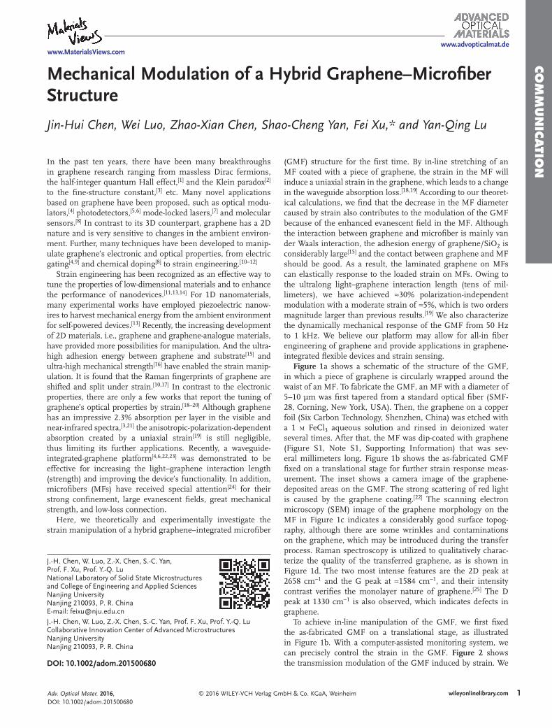
Figure 1a shows a schematic of the structure of the GMF, in which a piece of graphene is circularly wrapped around the waist of an MF. To fabricate the GMF, an MF with a diameter of 5–10 μm was first tapered from a standard optical fiber (SMF-28, Corning, New York, USA). Then, the graphene on a copper foil (Six Carbon Technology, Shenzhen, China) was etched with a 1 m FeCl3 aqueous solution and rinsed in deionized water several times. After that, the MF was dip-coated with graphene (Figure S1, Note S1, Supporting Information) that was sev-eral millimeters long. Figure 1b shows the as-fabricated GMF fixed on a translational stage for further strain response meas-urement. The inset shows a camera image of the graphene-deposited areas on the GMF. The strong scattering of red light is caused by the graphene coating.[22] The scanning electron microscopy (SEM) image of the graphene morphology on the MF in Figure 1c indicates a considerably good surface topog-raphy, although there are some wrinkles and contaminations on the graphene, which may be introduced during the transfer process. Raman spectroscopy is utilized to qualitatively charac-terize the quality of the transferred graphene, as is shown in Figure 1d. The two most intense features are the 2D peak at 2658 cm−1 and the G peak at ≈1584 cm−1, and their intensity contrast verifies the monolayer nature of graphene.[25] The D peak at 1330 cm−1 is also observed, which indicates defects in graphene.
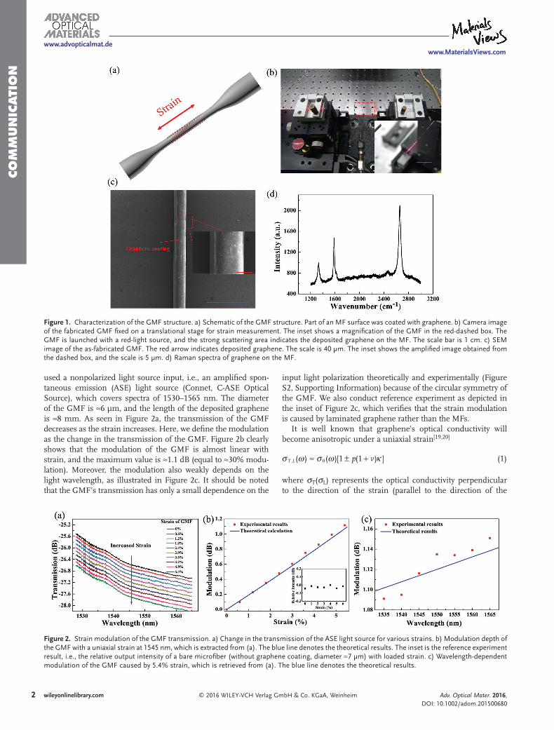
To achieve in-line manipulation of the GMF, we first fixed the as-fabricated GMF on a translational stage, as illustrated in Figure 1b. With a computer-assisted monitoring system, we can precisely control the strain in the GMF. Figure 2 shows the transmission modulation of the GMF induced by strain. We
Mechanical Modulation of a Hybrid Graphene–Microfiber Structure
Jin-Hui Chen, Wei Luo, Zhao-Xian Chen, Shao-Cheng Yan, Fei Xu,* and Yan-Qing Lu
J.-H. Chen, W. Luo, Z.-X. Chen, S.-C. Yan, Prof. F. Xu, Prof. Y.-Q. LuNational Laboratory of Solid State Microstructures and College of Engineering and Applied SciencesNanjing UniversityNanjing 210093, P. R. ChinaE-mail: [email protected]. Chen, W. Luo, Z.-X. Chen, S.-C. Yan, Prof. F. Xu, Prof. Y.-Q. LuCollaborative Innovation Center of Advanced MicrostructuresNanjing UniversityNanjing 210093, P. R. China
DOI: 10.1002/adom.201500680
In the past ten years, there have been many breakthroughs in graphene research ranging from massless Dirac fermions, the half-integer quantum Hall effect,[1] and the Klein paradox[2] to the fine-structure constant,[3] etc. Many novel applications based on graphene have been proposed, such as optical modu-lators,[4] photodetectors,[5,6] mode-locked lasers,[7] and molecular sensors.[8] In contrast to its 3D counterpart, graphene has a 2D nature and is very sensitive to changes in the ambient environ-ment. Further, many techniques have been developed to manip-ulate graphene’s electronic and optical properties, from electric gating[4,9] and chemical doping[8] to strain engineering.[10–12]
Strain engineering has been recognized as an effective way to tune the properties of low-dimensional materials and to enhance the performance of nanodevices.[11,13,14] For 1D nanomaterials, many experimental works have employed piezoelectric nanow-ires to harvest mechanical energy from the ambient environment for self-powered devices.[13] Recently, the increasing development of 2D materials, i.e., graphene and graphene-analogue materials, have provided more possibilities for manipulation. And the ultra-high adhesion energy between graphene and substrate[15] and ultra-high mechanical strength[16] have enabled the strain manip-ulation. It is found that the Raman fingerprints of graphene are shifted and split under strain.[10,17] In contrast to the electronic properties, there are only a few works that report the tuning of graphene’s optical properties by strain.[18–20] Although graphene has an impressive 2.3% absorption per layer in the visible and near-infrared spectra,[3,21] the anisotropic-polarization-dependent absorption created by a uniaxial strain[19] is still negligible, thus limiting its further applications. Recently, a waveguide-integrated-graphene platform[4,6,22,23] was demonstrated to be effective for increasing the light–graphene interaction length (strength) and improving the device’s functionality. In addition, microfibers (MFs) have received special attention[24] for their strong confinement, large evanescent fields, great mechanical strength, and low-loss connection.
Here, we theoretically and experimentally investigate the strain manipulation of a hybrid graphene–integrated microfiber
Adv. Optical Mater. 2016, DOI: 10.1002/adom.201500680
www.MaterialsViews.comwww.advopticalmat.de
2 wileyonlinelibrary.com © 2016 WILEY-VCH Verlag GmbH & Co. KGaA, Weinheim
CO
MM
UN
ICATI
ON
used a nonpolarized light source input, i.e., an amplified spon-taneous emission (ASE) light source (Connet, C-ASE Optical Source), which covers spectra of 1530–1565 nm. The diameter of the GMF is ≈6 μm, and the length of the deposited graphene is ≈8 mm. As seen in Figure 2a, the transmission of the GMF decreases as the strain increases. Here, we define the modulation as the change in the transmission of the GMF. Figure 2b clearly shows that the modulation of the GMF is almost linear with strain, and the maximum value is ≈1.1 dB (equal to ≈30% modu-lation). Moreover, the modulation also weakly depends on the light wavelength, as illustrated in Figure 2c. It should be noted that the GMF’s transmission has only a small dependence on the
input light polarization theoretically and experimentally (Figure S2, Supporting Information) because of the circular symmetry of the GMF. We also conduct reference experiment as depicted in the inset of Figure 2c, which verifies that the strain modulation is caused by laminated graphene rather than the MFs.
It is well known that graphene’s optical conductivity will become anisotropic under a uniaxial strain[19,20]
( ) ( )[1 (1 ) ]T, 0 p vLσ ω σ ω κ≈ ± + (1)
where σT(σL) represents the optical conductivity perpendicular to the direction of the strain (parallel to the direction of the
Adv. Optical Mater. 2016, DOI: 10.1002/adom.201500680
www.MaterialsViews.comwww.advopticalmat.de
Figure 1. Characterization of the GMF structure. a) Schematic of the GMF structure. Part of an MF surface was coated with graphene. b) Camera image of the fabricated GMF fixed on a translational stage for strain measurement. The inset shows a magnification of the GMF in the red-dashed box. The GMF is launched with a red-light source, and the strong scattering area indicates the deposited graphene on the MF. The scale bar is 1 cm. c) SEM image of the as-fabricated GMF. The red arrow indicates deposited graphene. The scale is 40 μm. The inset shows the amplified image obtained from the dashed box, and the scale is 5 μm. d) Raman spectra of graphene on the MF.
Figure 2. Strain modulation of the GMF transmission. a) Change in the transmission of the ASE light source for various strains. b) Modulation depth of the GMF with a uniaxial strain at 1545 nm, which is extracted from (a). The blue line denotes the theoretical results. The inset is the reference experiment result, i.e., the relative output intensity of a bare microfiber (without graphene coating, diameter ≈7 μm) with loaded strain. c) Wavelength-dependent modulation of the GMF caused by 5.4% strain, which is retrieved from (a). The blue line denotes the theoretical results.

3wileyonlinelibrary.com© 2016 WILEY-VCH Verlag GmbH & Co. KGaA, Weinheim
CO
MM
UN
ICATIO
N
strain), σ0 is the optical conductivity in the strain-free case, p is a numerical constant and ≈3–4,[20] v is the Poisson ratio, and κ is the strain magnitude. From (1), we can find that when the graphene sheet is under a uniaxial strain, its optical conductivity along the direction of the strain decreases while the transverse conductivity increases. Thus, when light nominally illuminates strained graphene, the light polarization transverse to the direction of the strain will suffer a larger absorption loss than the parallel one,[19] which leads to anisotropic polarization absorption.
However, things will be much different in the waveguide case. We developed a theoretical model[26] (Note S3, Supporting Information) to explain the observed phenomenon. First, most of the electric field (magnetic field) of the eigenmodes in the microfiber waveguide lie in the transverse plane. Thus, the longitu-dinal conductivity of graphene (in cylindrical coordinates) has a smaller influence than the
transverse optical conductivity on the wave-guide’s absorption loss caused by graphene. As a result, when the GMF is elongated in the axial direction, the strain-induced modula-tion of the waveguide’s transmission is domi-nated by the change in the transverse optical conductivity. As the transverse conductivity of graphene increases with the uniaxial strain, the waveguide transmission will naturally decrease with the increase of the strain, which is clearly illustrated in Figure 2. Second, thanks to the symmetry of the GMF, there theoretically will be no polarization-dependent absorption effect for the wave-guiding modes. However, the fabricated device has a small
polarization-dependent loss because of the defects in the sample. Interestingly, according to our theory, we find that the decrease in the diameter of the GMF caused by strain also contributes to the modulation phenomenon (Figure S4, Supporting Informa-tion), and its influence on the modulation of the GMF is compa-rable to the change in the optical conductivity of graphene. This is because the waveguide’s propagation loss is highly sensitive to this geometrical change, as shown in Figure 3a. The wavelength-dependent modulation relation can be attributed to the fact that the evanescent field strength of the MF has a weak wavelength dependence; that is, the longer input light wavelength of the GMF has a larger evanescent field to interact with the graphene coatings, and thus, a larger absorption loss (Figure 2a) and larger modulation (Figure 2c) are obtained. Our theoretical calculations agree well with the experimental data.
We also investigate the influence of the MF diameter on the strain-induced modulation of the GMF. Here, we define the modulation efficiency (ME) as the modulation per unit length of graphene-coated MF per 1% strain to quantitatively assess the impact of the MF diameter. It is clearly shown that the ME of the GMF exponentially decreases as the diameter increases in Figure 3a. As is known, the evanescent field strength decreases
Adv. Optical Mater. 2016, DOI: 10.1002/adom.201500680
www.MaterialsViews.comwww.advopticalmat.de
Figure 3. Strain-induced modulation relations with the diameter of the GMF. a) Propagation loss of the waveguide as a function of the diameter of the GMF at 1545 nm. b) Strain modula-tion efficiency of the GMF as a function of the diameter of the MF at 1545 nm.
Figure 4. Stable deformation cycling test of the GMF at 1535, 1545, and 1555 nm.
Figure 5. Dynamic mechanical-vibration-induced modulation of the GMF. The mechanical vibration response was tested at 50 Hz, 200 Hz, 500 Hz, and 1 kHz separately.
4 wileyonlinelibrary.com © 2016 WILEY-VCH Verlag GmbH & Co. KGaA, Weinheim
CO
MM
UN
ICATI
ON as the waveguide diameter increases. Accordingly, the light–
graphene interaction strength decreases as the diameter of the waveguide increases, and the ME of the strain is also naturally decreases. The stability and repeatability of our platform are also characterized, as illustrated in Figure 4. It is demonstrated that the strain cycling is repeatable and stable, which verifies that our device is elastically deformed. Further, the modula-tion effect has a weaker dependence on the light wavelength, as explicitly discussed above. To test the GMF’s dynamic strain response, we employed dynamic vibration of the GMF (Note S4, Supporting Information), as shown in Figure 5. Although the vibration frequencies only cover 50–1000 Hz, we believe that it can achieve a modulation speed of hundreds of kilohertz by fur-ther careful design. The broadband, polarization-independent, cost-effective strain modulator may find applications in low-speed modulation, strain sensing, and waveguide design.
It has been proposed that the uniaxial-strain manipulation of a graphene sheet can lead to the anisotropic optical conductivity of graphene. Here, we investigate waveguide-based amplification due to the strain effect in graphene for the first time. We theoreti-cally analyze the influential factors of strain tuning, such as the geometrical parameters of the MF, the magnitude of the strain, and the light wavelength. Further, we experimentally achieve modulation as high as 30% with a moderate strain of ≈5%, which is two orders of magnitude larger than previous results. More-over, the modulation can be further improved, e.g., by tuning the encapsulated graphene length, the diameter of the MF, and the employed strain. It should be noted that graphene can be elasti-cally deformed to a strain as high as 25%,[27] which indicates the great potential of strain manipulation for waveguide-integrated graphene. Our method can also easily extend to other graphene analogous materials or graphene derivatives.[28] It is found that fluorinated, hydrogenated, and oxidized graphene show enhanced nanoscale friction on their surfaces, which is beneficial for our in-line strain manipulation. We believe our platform may allow for the all-in fiber engineering of graphene and provide new ideas for graphene-integrated flexible devices and strain sensing.
Experimental SectionSEM and Raman Measurements: The surface morphology of the
graphene transferred onto an MF was characterized by a dual beam focus ion beam system (FIB) 235, FEI Strata. Raman spectra were obtained by a Horiba John Yvon HR800 system with a laser excitation wavelength of 633 nm.
Strain Response Measurement: The in-line stretching of the GMF was generated by a linear motor stage with a travel distance of 350 mm (XML, Newport). The dynamic vibration was produced by a homemade speaker with its output controlled by a program. A CW laser (Agilent, tunable laser 81980 A) was employed as the probe light source and the modulated output light was detected by a photo-detector (New Focus, 1544-B). The transformed electric signal could be analyzed by an oscilloscope (Agilent Technologies, DSO-X 4024A).
Supporting InformationSupporting Information is available from the Wiley Online Library or from the author.
AcknowledgementsThe authors thank Yue-Hui Chen and Prof. Xue-Jin Zhang for helping Raman characterizations. The SEM was supported by Ying-Ling Tan. This work was sponsored by National 973 program (2012CB921803) and National Natural Science Foundation of China (61322503, 61535005, 61225026, and 61475069).
Received: November 18, 2015Revised: January 29, 2016
Published online:
[1] K. Novoselov, A. K. Geim, S. Morozov, D. Jiang, M. Katsnelson, I. Grigorieva, S. Dubonos, A. Firsov, Nature 2005, 438, 197.
[2] M. Katsnelson, K. Novoselov, A. Geim, Nat. Phys. 2006, 2, 620.[3] R. R. Nair, P. Blake, A. N. Grigorenko, K. S. Novoselov, T. J. Booth,
T. Stauber, N. M. R. Peres, A. K. Geim, Science 2008, 320, 1308.[4] M. Liu, X. Yin, E. Ulin-Avila, B. Geng, T. Zentgraf, L. Ju, F. Wang,
X. Zhang, Nature 2011, 474, 64.[5] a) F. Xia, T. Mueller, Y.-M. Lin, A. Valdes-Garcia, P. Avouris,
Nat. Nanotechnol. 2009, 4, 839; b) T. Mueller, F. Xia, P. Avouris, Nat. Photonics 2010, 4, 297.
[6] X. Gan, R.-J. Shiue, Y. Gao, I. Meric, T. F. Heinz, K. Shepard, J. Hone, S. Assefa, D. Englund, Nat. Photonics 2013, 7, 883.
[7] Z. Sun, T. Hasan, F. Torrisi, D. Popa, G. Privitera, F. Wang, F. Bonaccorso, D. M. Basko, A. C. Ferrari, ACS Nano 2010, 4, 803.
[8] F. Schedin, A. Geim, S. Morozov, E. Hill, P. Blake, M. Katsnelson, K. Novoselov, Nat. Mater. 2007, 6, 652.
[9] F. Wang, Y. Zhang, C. Tian, C. Girit, A. Zettl, M. Crommie, Y. R. Shen, Science 2008, 320, 206.
[10] Z. H. Ni, T. Yu, Y. H. Lu, Y. Y. Wang, Y. P. Feng, Z. X. Shen, ACS Nano 2008, 2, 2301.
[11] a) V. M. Pereira, A. C. Neto, Phys. Rev. Lett. 2009, 103, 046801; b) N. Levy, S. Burke, K. Meaker, M. Panlasigui, A. Zettl, F. Guinea, A. C. Neto, M. Crommie, Science 2010, 329, 544.
[12] F. Guinea, M. Katsnelson, A. Geim, Nat. Phys. 2010, 6, 30.[13] a) Z. L. Wang, J. Song, Science 2006, 312, 242; b) S. Xu,
Y. Qin, C. Xu, Y. Wei, R. Yang, Z. L. Wang, Nat. Nanotechnol. 2010, 5, 366.
[14] a) H. Zhu, Y. Wang, J. Xiao, M. Liu, S. Xiong, Z. J. Wong, Z. Ye, Y. Ye, X. Yin, X. Zhang, Nat. Nanotechnol. 2015, 10, 151; b) W. Wu, L. Wang, Y. Li, F. Zhang, L. Lin, S. Niu, D. Chenet, X. Zhang, Y. Hao, T. F. Heinz, Nature 2014, 514, 470.
[15] S. P. Koenig, N. G. Boddeti, M. L. Dunn, J. S. Bunch, Nat. Nanotechnol. 2011, 6, 543.
[16] C. Lee, X. Wei, J. W. Kysar, J. Hone, Science 2008, 321, 385.[17] T. Mohiuddin, A. Lombardo, R. Nair, A. Bonetti, G. Savini, R. Jalil,
N. Bonini, D. Basko, C. Galiotis, N. Marzari, Phys. Rev. B 2009, 79, 205433.
[18] F. Pellegrino, G. Angilella, R. Pucci, Phys. Rev. B 2010, 81, 035411.[19] G. X. Ni, H. Z. Yang, W. Ji, S. J. Baeck, C. T. Toh, J. H. Ahn,
V. M. Pereira, B. Özyilmaz, Adv. Mater. 2014, 26, 1081.[20] V. M. Pereira, R. Ribeiro, N. Peres, A. C. Neto, EPL 2010, 92,
67001.[21] K. F. Mak, M. Y. Sfeir, Y. Wu, C. H. Lui, J. A. Misewich, T. F. Heinz,
Phys. Rev. Lett. 2008, 101, 196405.[22] W. Li, B. Chen, C. Meng, W. Fang, Y. Xiao, X. Li, Z. Hu, Y. Xu,
L. Tong, H. Wang, Nano Lett. 2014, 14, 955.[23] a) J.-L. Kou, J.-H. Chen, Y. Chen, F. Xu, Y.-Q. Lu, Optica 2014, 1,
307; b) Q. Bao, H. Zhang, B. Wang, Z. Ni, C. H. Y. X. Lim, Y. Wang, D. Y. Tang, K. P. Loh, Nat. Photonics 2011, 5, 411.
Adv. Optical Mater. 2016, DOI: 10.1002/adom.201500680
www.MaterialsViews.comwww.advopticalmat.de

5wileyonlinelibrary.com© 2016 WILEY-VCH Verlag GmbH & Co. KGaA, Weinheim
CO
MM
UN
ICATIO
N
Adv. Optical Mater. 2016, DOI: 10.1002/adom.201500680
www.MaterialsViews.comwww.advopticalmat.de
[24] a) L. Tong, R. R. Gattass, J. B. Ashcom, S. He, J. Lou, M. Shen, I. Maxwell, E. Mazur, Nature 2003, 426, 816; b) G. Brambilla, F. Xu, P. Horak, Y. Jung, F. Koizumi, N. P. Sessions, E. Koukharenko, X. Feng, G. S. Murugan, J. S. Wilkinson, Adv. Opt. Photonics 2009, 1, 107.
[25] A. Ferrari, J. Meyer, V. Scardaci, C. Casiraghi, M. Lazzeri, F. Mauri, S. Piscanec, D. Jiang, K. Novoselov, S. Roth, Phys. Rev. Lett. 2006, 97, 187401.
[26] Y. Gao, G. Ren, B. Zhu, H. Liu, Y. Lian, S. Jian, Opt. Express 2014, 22, 24322.
[27] K. S. Kim, Y. Zhao, H. Jang, S. Y. Lee, J. M. Kim, K. S. Kim, J.-H. Ahn, P. Kim, J.-Y. Choi, B. H. Hong, Nature 2009, 457, 706.
[28] a) S. Kwon, J.-H. Ko, K.-J. Jeon, Y.-H. Kim, J. Y. Park, Nano Lett. 2012, 12, 6043; b) J.-H. Ko, S. Kwon, I.-S. Byun, J. S. Choi, B. H. Park, Y.-H. Kim, J. Y. Park, Tribol. Lett. 2013, 50, 137.